EP2393080A1 - Charge storage circuit for a pixel, and a display - Google Patents
Charge storage circuit for a pixel, and a display Download PDFInfo
- Publication number
- EP2393080A1 EP2393080A1 EP11168815A EP11168815A EP2393080A1 EP 2393080 A1 EP2393080 A1 EP 2393080A1 EP 11168815 A EP11168815 A EP 11168815A EP 11168815 A EP11168815 A EP 11168815A EP 2393080 A1 EP2393080 A1 EP 2393080A1
- Authority
- EP
- European Patent Office
- Prior art keywords
- transistor
- voltage
- circuit
- charge storage
- gate
- Prior art date
- Legal status (The legal status is an assumption and is not a legal conclusion. Google has not performed a legal analysis and makes no representation as to the accuracy of the status listed.)
- Granted
Links
Images


Classifications
-
- G—PHYSICS
- G09—EDUCATION; CRYPTOGRAPHY; DISPLAY; ADVERTISING; SEALS
- G09G—ARRANGEMENTS OR CIRCUITS FOR CONTROL OF INDICATING DEVICES USING STATIC MEANS TO PRESENT VARIABLE INFORMATION
- G09G3/00—Control arrangements or circuits, of interest only in connection with visual indicators other than cathode-ray tubes
- G09G3/20—Control arrangements or circuits, of interest only in connection with visual indicators other than cathode-ray tubes for presentation of an assembly of a number of characters, e.g. a page, by composing the assembly by combination of individual elements arranged in a matrix no fixed position being assigned to or needed to be assigned to the individual characters or partial characters
- G09G3/34—Control arrangements or circuits, of interest only in connection with visual indicators other than cathode-ray tubes for presentation of an assembly of a number of characters, e.g. a page, by composing the assembly by combination of individual elements arranged in a matrix no fixed position being assigned to or needed to be assigned to the individual characters or partial characters by control of light from an independent source
- G09G3/36—Control arrangements or circuits, of interest only in connection with visual indicators other than cathode-ray tubes for presentation of an assembly of a number of characters, e.g. a page, by composing the assembly by combination of individual elements arranged in a matrix no fixed position being assigned to or needed to be assigned to the individual characters or partial characters by control of light from an independent source using liquid crystals
- G09G3/3611—Control of matrices with row and column drivers
- G09G3/3648—Control of matrices with row and column drivers using an active matrix
-
- G—PHYSICS
- G02—OPTICS
- G02F—OPTICAL DEVICES OR ARRANGEMENTS FOR THE CONTROL OF LIGHT BY MODIFICATION OF THE OPTICAL PROPERTIES OF THE MEDIA OF THE ELEMENTS INVOLVED THEREIN; NON-LINEAR OPTICS; FREQUENCY-CHANGING OF LIGHT; OPTICAL LOGIC ELEMENTS; OPTICAL ANALOGUE/DIGITAL CONVERTERS
- G02F1/00—Devices or arrangements for the control of the intensity, colour, phase, polarisation or direction of light arriving from an independent light source, e.g. switching, gating or modulating; Non-linear optics
- G02F1/01—Devices or arrangements for the control of the intensity, colour, phase, polarisation or direction of light arriving from an independent light source, e.g. switching, gating or modulating; Non-linear optics for the control of the intensity, phase, polarisation or colour
- G02F1/13—Devices or arrangements for the control of the intensity, colour, phase, polarisation or direction of light arriving from an independent light source, e.g. switching, gating or modulating; Non-linear optics for the control of the intensity, phase, polarisation or colour based on liquid crystals, e.g. single liquid crystal display cells
- G02F1/133—Constructional arrangements; Operation of liquid crystal cells; Circuit arrangements
- G02F1/136—Liquid crystal cells structurally associated with a semi-conducting layer or substrate, e.g. cells forming part of an integrated circuit
- G02F1/1362—Active matrix addressed cells
- G02F1/136213—Storage capacitors associated with the pixel electrode
-
- G—PHYSICS
- G09—EDUCATION; CRYPTOGRAPHY; DISPLAY; ADVERTISING; SEALS
- G09G—ARRANGEMENTS OR CIRCUITS FOR CONTROL OF INDICATING DEVICES USING STATIC MEANS TO PRESENT VARIABLE INFORMATION
- G09G3/00—Control arrangements or circuits, of interest only in connection with visual indicators other than cathode-ray tubes
- G09G3/20—Control arrangements or circuits, of interest only in connection with visual indicators other than cathode-ray tubes for presentation of an assembly of a number of characters, e.g. a page, by composing the assembly by combination of individual elements arranged in a matrix no fixed position being assigned to or needed to be assigned to the individual characters or partial characters
- G09G3/22—Control arrangements or circuits, of interest only in connection with visual indicators other than cathode-ray tubes for presentation of an assembly of a number of characters, e.g. a page, by composing the assembly by combination of individual elements arranged in a matrix no fixed position being assigned to or needed to be assigned to the individual characters or partial characters using controlled light sources
- G09G3/30—Control arrangements or circuits, of interest only in connection with visual indicators other than cathode-ray tubes for presentation of an assembly of a number of characters, e.g. a page, by composing the assembly by combination of individual elements arranged in a matrix no fixed position being assigned to or needed to be assigned to the individual characters or partial characters using controlled light sources using electroluminescent panels
- G09G3/32—Control arrangements or circuits, of interest only in connection with visual indicators other than cathode-ray tubes for presentation of an assembly of a number of characters, e.g. a page, by composing the assembly by combination of individual elements arranged in a matrix no fixed position being assigned to or needed to be assigned to the individual characters or partial characters using controlled light sources using electroluminescent panels semiconductive, e.g. using light-emitting diodes [LED]
- G09G3/3208—Control arrangements or circuits, of interest only in connection with visual indicators other than cathode-ray tubes for presentation of an assembly of a number of characters, e.g. a page, by composing the assembly by combination of individual elements arranged in a matrix no fixed position being assigned to or needed to be assigned to the individual characters or partial characters using controlled light sources using electroluminescent panels semiconductive, e.g. using light-emitting diodes [LED] organic, e.g. using organic light-emitting diodes [OLED]
- G09G3/3225—Control arrangements or circuits, of interest only in connection with visual indicators other than cathode-ray tubes for presentation of an assembly of a number of characters, e.g. a page, by composing the assembly by combination of individual elements arranged in a matrix no fixed position being assigned to or needed to be assigned to the individual characters or partial characters using controlled light sources using electroluminescent panels semiconductive, e.g. using light-emitting diodes [LED] organic, e.g. using organic light-emitting diodes [OLED] using an active matrix
-
- G—PHYSICS
- G09—EDUCATION; CRYPTOGRAPHY; DISPLAY; ADVERTISING; SEALS
- G09G—ARRANGEMENTS OR CIRCUITS FOR CONTROL OF INDICATING DEVICES USING STATIC MEANS TO PRESENT VARIABLE INFORMATION
- G09G2300/00—Aspects of the constitution of display devices
- G09G2300/04—Structural and physical details of display devices
- G09G2300/0439—Pixel structures
- G09G2300/0465—Improved aperture ratio, e.g. by size reduction of the pixel circuit, e.g. for improving the pixel density or the maximum displayable luminance or brightness
-
- G—PHYSICS
- G09—EDUCATION; CRYPTOGRAPHY; DISPLAY; ADVERTISING; SEALS
- G09G—ARRANGEMENTS OR CIRCUITS FOR CONTROL OF INDICATING DEVICES USING STATIC MEANS TO PRESENT VARIABLE INFORMATION
- G09G2300/00—Aspects of the constitution of display devices
- G09G2300/08—Active matrix structure, i.e. with use of active elements, inclusive of non-linear two terminal elements, in the pixels together with light emitting or modulating elements
- G09G2300/0809—Several active elements per pixel in active matrix panels
- G09G2300/0814—Several active elements per pixel in active matrix panels used for selection purposes, e.g. logical AND for partial update
-
- G—PHYSICS
- G09—EDUCATION; CRYPTOGRAPHY; DISPLAY; ADVERTISING; SEALS
- G09G—ARRANGEMENTS OR CIRCUITS FOR CONTROL OF INDICATING DEVICES USING STATIC MEANS TO PRESENT VARIABLE INFORMATION
- G09G2300/00—Aspects of the constitution of display devices
- G09G2300/08—Active matrix structure, i.e. with use of active elements, inclusive of non-linear two terminal elements, in the pixels together with light emitting or modulating elements
- G09G2300/0809—Several active elements per pixel in active matrix panels
- G09G2300/0833—Several active elements per pixel in active matrix panels forming a linear amplifier or follower
-
- G—PHYSICS
- G09—EDUCATION; CRYPTOGRAPHY; DISPLAY; ADVERTISING; SEALS
- G09G—ARRANGEMENTS OR CIRCUITS FOR CONTROL OF INDICATING DEVICES USING STATIC MEANS TO PRESENT VARIABLE INFORMATION
- G09G3/00—Control arrangements or circuits, of interest only in connection with visual indicators other than cathode-ray tubes
- G09G3/20—Control arrangements or circuits, of interest only in connection with visual indicators other than cathode-ray tubes for presentation of an assembly of a number of characters, e.g. a page, by composing the assembly by combination of individual elements arranged in a matrix no fixed position being assigned to or needed to be assigned to the individual characters or partial characters
- G09G3/34—Control arrangements or circuits, of interest only in connection with visual indicators other than cathode-ray tubes for presentation of an assembly of a number of characters, e.g. a page, by composing the assembly by combination of individual elements arranged in a matrix no fixed position being assigned to or needed to be assigned to the individual characters or partial characters by control of light from an independent source
- G09G3/36—Control arrangements or circuits, of interest only in connection with visual indicators other than cathode-ray tubes for presentation of an assembly of a number of characters, e.g. a page, by composing the assembly by combination of individual elements arranged in a matrix no fixed position being assigned to or needed to be assigned to the individual characters or partial characters by control of light from an independent source using liquid crystals
- G09G3/3611—Control of matrices with row and column drivers
- G09G3/3648—Control of matrices with row and column drivers using an active matrix
- G09G3/3659—Control of matrices with row and column drivers using an active matrix the addressing of the pixel involving the control of two or more scan electrodes or two or more data electrodes, e.g. pixel voltage dependant on signal of two data electrodes
Definitions
- the invention is a low leakage charge storage circuit, suitable for use in, for example, an active matrix display, a DRAM etc. It also relates to a display incorporating one or more charge storage circuits of the invention.
- FIG 1 shows a typical active matrix display.
- Such a display is made up of a matrix 2 of picture elements (pixels), arranged in M rows and N columns. Each pixel row [column] is connected to a respective row [column] electrode, with the column electrodes being connected to the N outputs of a data driver 4 and the row electrodes being connected to the M outputs of a scan driver 6.
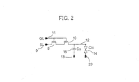
- the circuit of a typical pixel in a liquid crystal display (LCD) is shown in figure 2 .
- the pixel comprises a display element 14 which is connected in parallel to a storage capacitor 16 via a common node 12 (also referred to below as a "charge storage node” or “storage node”).
- the other terminal of the storage capacitor 16 is connected to a common electrode 18, which may in use act as a capacitor bias line.
- the display element may comprise a pixel electrode which is electrically connected to the charge storage node 12 (and in this case the pixel electrode may constitute the charge storage node 12), and the other terminal of the display element 14 is connected to a counter plate electrode 20.
- the charge storage node 12 is also connected to the drain of a transistor 10.
- the source of transistor 10 is connected to the drain of a transistor 8.
- the source of transistor 8 is connected to a common source line 9 which is driven by one of the outputs from the data driver 4.
- the gates of 2 series connected transistor 8, 10 are connected together to a gate line 11 which is common to all the pixels of the row and which is connected to a respective output of the scan driver 6.
- rows of pixel display data are supplied by the data driver 4 to the source electrodes 9 in synchronism with scan pulses which are supplied by the scan driver 6 to the gate lines 11 in a cyclically repeating sequence.
- scan pulses which are supplied by the scan driver 6 to the gate lines 11 in a cyclically repeating sequence.
- the row of pixels are refreshed one at a time until all of the rows have been refreshed so as to complete the refreshing of a frame of display data. The process is then repeated for the next frame of data.
- each pixel When the gate line 11 of each pixel receives a scan pulse from the scan driver 6, the voltage on the source electrode 9 causes the storage capacitor 16, and the pixel electrode of the display element, to be charged.
- the transistors 8, 10 isolate the pixel electrode and the storage capacitor from the source electrode 9 so that the optical property of the associated display element 14 corresponds to the stored voltage across the display element 14 until it is refreshed during the next frame.
- the voltage across the display element 14 is not necessarily equal to the voltage across the storage capacitor 16, since the counter plate electrode 20 of the display element 14 and the second plate 18 of the storage capacitor 16 may be at different potentials to one another.
- Capacitively coupled driving in which the signal data voltage is supplied to the pixel electrode from the source electrode 9, via transistors 8, 10, during the period the gate line 11 of each pixel receives a scan pulse from the scan driver 6, in order to charge the pixel electrode and storage capacitor 16 to the voltage of the data signal, and then after the scan pulse is removed, an offset is imposed to the data voltage on the pixel electrode via capacitive coupling to the pixel electrode of a second voltage applied to the second plate 18 of the storage capacitor 16, is described in EP0336570A1 (11 October 1989 ) and US patent 5296847 (22 March 1994 , Matsushita) and in Tsunashima et al, SID Digest '07, pp 1014 -1017 .
- the isolation transistors 8, 10 are not perfect. They exhibit a finite leakage drain current as illustrated in Figure 3 which shows the typical transfer characteristic of an NMOS transistor.
- the leakage current in the transistor is a function of the drain to source (Vds) and gate to source (Vgs) potentials.
- the pixel electrode voltage degradation due to leakage current requires the display data to be rewritten to minimise image deterioration during the hold time.
- a frame refresh rate of 60Hz is typical. This constant refreshing of the display results in significant power consumption.
- One approach to reducing this power consumption is to reduce the frame refresh rate. Frame rate reduction is only possible if the degradation of the pixel electrode voltage is reduced.
- the pixel electrode voltage degradation can be reduced by either increasing the size of the storage capacitor 16 or reducing the leakage current. A larger storage capacitor 16 is not desirable since it would result in increased pixel area and also increased pixel electrode charging time during scanning of each row.
- the preferred approach to reducing the frame refresh rate is to reduce the leakage current.
- One known technique for reducing the electric field induced leakage current is to replace the 2 series transistors 8 and 10 with 3 or more transistors in series. This is in order to further reduce the drain voltage for each transistor. It may be noted however that the common gate voltage means that the leakage current does not scale with the number of series transistors.
- Another known technique, shown in Figure 4 is to use an additional hold capacitor 15 at the junction of the series connected transistors 8, 10. This technique does not provide sufficient reduction in leakage current to enable reduction of frame refresh rate.
- Figure 5(a) illustrates another technique to increase the hold time over several frames as disclosed in Japanese laid-open patent application No. 5-142573 (11 June 1993 ).
- This technique involves "boot strapping”: a unity gain voltage gain amplifier 22 has its input connected to the charge storage node 12 and the pixel electrode and its output connected to the junction between transistors 8 and 10.
- the circuit of Figure 5(a) is provided with a feedback function through the unity gain voltage amplifier 22, so that the pixel electrode voltage appears at the junction of the series connected transistors 8 and 10. If the buffer amplifier 22 were ideal and drew no charge from the pixel electrode, leakage from the pixel electrode would be eliminated since the drain to source voltage of transistor 10 would be reduced to zero volts.
- buffer amplifier 22 circuits disclosed shown in Figure 5(b) include a CMOS source follower circuit 24 that combines an NMOS transistor and a PMOS transistor, a CMOS 2 stage source follower circuit 26 and voltage follower circuit that uses an operational amplifier 28. All of the proposed implementations of the buffer amplifier 22 result in at least 2 additional transistors and 2 power supply lines which results in an increase in the pixel circuit area. The additional transistors will reduce the yield during the fabrication of the display. Further, the increased active pixel area limits the minimum achievable pixel size and therefore limits the maximum resolution of the display. If a display is of a transmissive or transflective type, the increased active area of the pixel results in reduced light transmission from the backlight through the pixels which reduces the brightness of the display.
- US patents 6064362 (16 May 2000 ) and 7573451 (11 August 2009 ) disclose a pixel circuit with a feedback buffer amplifier which as in the Japanese laid-open patent application No. 5-142573 aims to reduce the leakage from the storage node.
- the buffer amplifier in both disclosures consists of at least 2 additional transistors.
- Figure 3 illustrates typical n-channel transistor input characteristics.
- the drain current initially increases exponentially - and then flattens out (meaning that the rate of increase of the drain current with gate voltage becomes lower for higher gate voltages).
- This exponentially increasing characteristic is the subthreshold region of the transistor operation.
- the figure also shows the dependence of the drain current on the drain potential. In the subthreshold region, the gate voltage has a significantly greater influence upon the drain current compared with the drain voltage. For example, 0.25V change in gate voltage results in 40 times change in the drain current whereas an 8V change in the drain voltage is necessary to achieve the same drain current change.
- a first aspect of the invention provides a charge storage circuit for a pixel, the circuit comprising: a charge storage node; first and second transistors for selectively isolating the charge storage node from a first voltage input for supplying a data voltage, the first and second transistors being series-connected; and a voltage follower circuit for replicating a voltage at the charge storage node (12) at another node in the circuit such that the drain-source voltage across the second transistor is reduced; wherein the voltage follower circuit comprises the first transistor.
- the present invention employs a voltage follower to reduce the leakage current through the first and second transistors, which are isolation transistors for isolating, in a voltage holding mode, the charge storage node from the voltage input.
- the voltage follower replicates, as closely as possible, the voltage at the charge storage node at another node in the circuit so that the drain-source voltage across the second transistor is reduced.
- the drain-source voltage across the second transistor preferably reduced to zero or almost to zero (and is reduced to zero if the voltage follower circuit exactly replicate the voltage at the charge storage node (12) at the other node).
- this reduction in the drain-source voltage across the second transistor leads to a reduction in the leakage current through the second transistor (and in principle the leakage current through the second transistor may be reduced to zero if the drain-source voltage across the second transistor is reduced to zero).
- one of the isolation transistors is used as part of the voltage follower, thereby reducing the number of additional components that must be provided for the voltage follower and also reducing the area occupied by the voltage follower. The invention thus reduces the leakage current, and hence reduces the required frame refresh rate, for little or no increase in the area of the pixel.
- FIG. 6 A first embodiment is shown in Figure 6 . This consists of a pixel circuit for an active matrix display.
- the circuit contains the following elements:
- a load element Clc 14 representing the impedance of the optical element between the charge storage node 12 and the counter plate node 20 in the case of a liquid crystal display.
- the counter plate node 20 may be common to all pixels of the display and so form a common electrode.
- the circuit is connected as follows:
- the voltage writing mode is the same as that of a standard active matrix display described in the prior art, for example is the same as described above with reference to the circuit of figure 2 . That is, when the gate line 11 of each pixel receives a scan pulse from the scan driver 6, the transistors 8, 10 are turned ON and electrically connect the source electrode 9 to the charge storage node (pixel electrode) 12 so that the voltage on the source electrode 9 causes the pixel electrode of the display element and the storage capacitor 16 to be charged. When the scan pulse is removed, the first and second transistors 8, 10 are turned OFF and isolate the pixel electrode and charge storage node 12 from the source electrode 9 so that the optical property of the associated display element 14 corresponds to the voltage across the display element 14 until it is refreshed during the next frame. Thus, the first and second transistors 8, 10 selectively isolate the charge storage node 12 from a voltage input (ie, from the source electrode 9).
- an offset may be imposed to the data voltage on the pixel electrode via capacitive coupling to the pixel electrode of a second voltage applied to the second plate 18 of the storage capacitor 16.
- the voltage holding mode is, in this embodiment, enabled once all rows of the pixel matrix have been written.
- the source line 9 is programmed by the scan driver 6 at a voltage which biases the first transistor 8 in the subthreshold region.
- This voltage is preferably set to be the same as the low level of the gate line 11 voltage, resulting in the first transistor biased with zero volts gate-source voltage (Vgs).
- the power supply line 32 is, in use, maintained at a voltage level higher than the highest data voltage during the hold mode (and also during the write function as well). With these bias conditions the third transistor 30 and first transistor 8 forms a voltage follower with the input being the data voltage written on to the storage node 12 and the output connected to the source of the second transistor 8.
- the Vgs of the first transistor 8 may be set to a non-zero value to allow optimisation of the bias current and therefore the power consumption. (The amount by which the voltage Vgs may vary from zero will depend on the transistor process conditions, but typically may vary from zero by up to a few hundred millivolts.)
- the voltage follower replicates, as closely as possible, the voltage at the charge storage node at another node in the circuit so that the drain-source voltage across the second transistor 10 is reduced, and preferably is reduced to zero or almost to zero.
- the voltage follower may for example replicate the voltage at the charge storage node at a node between the first transistor 8 and the second transistor 10. As a result the leakage current through the second transistor 10 is reduced (and would be reduced to zero if the drain-source voltage across the second transistor 10 is reduced to zero).
- the voltage follower operates as follows:
- the write function is repeated when the storage node data requires updating.
- this embodiment could also be implemented with the second transistor 10 formed as a dual gate transistor 10a, 10b as shown in Figure 7 .
- This implementation further reduces the leakage current from the storage node compared with a single gate transistor 10. Since the node at the source of transistor 8 is biased, the dual gate transistor 10a, 10b has the same electric field reduction effect as a standard pixel circuit shown in Figure 2 .
- FIG. 8 A second embodiment is shown in Figure 8 .
- This embodiment is identical to the first embodiment except transistor 8 is replaced by two series connected transistors 8a, 8b whose gates are connected to the gate line 11 and transistor 30 is replaced by two series connected transistors 30a, 30b whose gates are connected to the storage node 12.
- the operation of the circuit is the same as the first embodiment.
- the voltage follower which is necessary for the voltage holding mode is now formed by the four transistors 8a, 8b, 30a and 30b.
- This voltage follower operates as follows:
- Vpix For the case of a high value pixel electrode voltage, Vpix:
- transistor 8b has absorbed a large Vds which results in transistors 8a and 30b having very similar bias conditions.
- Vpix For the case of a low value pixel electrode voltage, Vpix:
- transistor 30a has absorbed a large Vds which results in transistors 8a and 30b having very similar bias conditions.
- a third embodiment is shown in Figure 9 .
- This embodiment is identical to the first embodiment except the gate line 11 is split into 2 separate gate lines 11 a and 11 b.
- a first gate line 11 a is connected to the gate of the first transistor 8 and a second gate line 11 b is connected to the gate of the second transistor 10.
- the operation of this embodiment is the same as the first embodiment except the first and second gate lines 11 a and 11b are driven separately.
- the driving voltages of both the gate lines are typically the same. However, there may be instances when it is desirable to independently control the bias voltage on the gate of transistor 8 and the switching voltage on the gate of transistor 10.
- the advantage of this embodiment is that the separate gate lines 11a, 11b allow independent control of the voltage follower bias voltage on the first gate line 11 a and therefore the bias current of the voltage follower. Additionally, the voltage on the second gate line 11b may also be adjusted to ensure that transistor 10 operates at the minimum leakage point. The power consumption and operating point of the pixel circuit may therefore be optimised using this embodiment.
- a fourth embodiment is shown in Figure 10 , and is identical to the first embodiment except two additional transistors 34, 36 and one bias line 13 has been added.
- the polarity of the channel of the fifth transistor 34 is opposite of the rest of the transistors in the pixel circuit.
- transistor 34 is p-type and the rest of the transistors in the pixel circuit are n-type.
- the source of the fourth transistor 36 is connected to the source line 9.
- the drain of the fourth transistor 36 is connected to the source of the first transistor 8.
- the gate of the fourth transistor 36 is connected to the gate line 11.
- the source of the fifth transistor 34 is connected to the bias line 13 (which forms a third voltage input), its drain is connected to a second node between the first transistor and the fourth transistor 36 (in this embodiment the second node is between the source of the first transistor 8 and the drain of the fourth transistor 36), and the gate of the fifth transistor 34 is connected to the gate line 11.
- the circuit performs two functions, writing a voltage to the storage node 12 and holding the voltage written on to the storage node 12.
- the write function is the same as the previous embodiments except transistor 34 is switched off when the gate line 11 receives a scan pulse from the scan driver 6.
- the write operation on each row is completed when the scan pulse is removed from the gate line 11 to switch off the two transistors 10, 36.
- This step also switches on transistor 34.
- the voltage holding mode is enabled on a row by row basis immediately after each row has been written.
- the switched on transistor 34 passes the bias line 13 voltage to the source of transistor 8.
- transistors 8 and 30 form a voltage follower with transistor 8 biased in the subthreshold region with a typical 0V Vgs.
- An advantage of this embodiment is that once a pixel been written, the voltage holding mode can be activated immediately by using the bias line 13 to bias the voltage follower.
- Source line 9 can continue to be used to write to pixels of other rows of the active matrix display. Pixel electrode voltage degradation due to source line voltage variations is thus avoided. (The pixel area in this embodiment is likely to be greater than in other embodiments, owing to the need for the additional supply line and transistors.)
- this embodiment could also be implemented with the transistor 34 formed as an n-type transistor. In this case a separate gate line is required to control the switch transistor 34. This gate line is then driven with voltage signals that are complementary to those applied to gate line 11.
- a circuit of the invention may be applied in an active matrix LCD, for example to the AMLCD of figure 1 .
- each pixel of AMLCD may have a circuit of the present invention.
- any of the previous embodiments are not restricted to active matrix LCD.
- the embodiments may be applied to other active matrix display technologies such as organic light emitting diode (OLED) displays, micro electro-mechanical (MEMs) displays and electro-wetting displays.
- OLED organic light emitting diode
- MEMs micro electro-mechanical
- electro-wetting displays The embodiments may be applied as a single circuit or as part of an array or as part of a matrix which is used to store voltage data.
- DRAM dynamic random access memories
- a first aspect of the invention provides a charge storage circuit for a pixel, the circuit comprising: a charge storage node; first and second transistors for selectively isolating the charge storage node from a first voltage input for supplying a data voltage, the first and second transistors being series-connected; and a voltage follower circuit for replicating a voltage at the charge storage node (12) at another node in the circuit such that the drain-source voltage across the second transistor is reduced; wherein the voltage follower circuit comprises the first transistor.
- the present invention employs a voltage follower to reduce the leakage current through the first and second transistors, which are isolation transistors for isolating, in a voltage holding mode, the charge storage node from the voltage input.
- the voltage follower replicates, as closely as possible, the voltage at the charge storage node at another node in the circuit so that the drain-source voltage across the second transistor is reduced.
- the drain-source voltage across the second transistor preferably reduced to zero or almost to zero (and is reduced to zero if the voltage follower circuit exactly replicate the voltage at the charge storage node (12) at the other node).
- this reduction in the drain-source voltage across the second transistor leads to a reduction in the leakage current through the second transistor (and in principle the leakage current through the second transistor may be reduced to zero if the drain-source voltage across the second transistor is reduced to zero).
- one of the isolation transistors is used as part of the voltage follower, thereby reducing the number of additional components that must be provided for the voltage follower and also reducing the area occupied by the voltage follower. The invention thus reduces the leakage current, and hence reduces the required frame refresh rate, for little or no increase in the area of the pixel.
- the first and second transistors may be connected in series between the first voltage input and the charge storage node, the second transistor being connected between the first transistor and the charge storage node.
- the voltage follower may replicates, as closely as possible, the voltage at the charge storage node at a node between the first transistor and the second transistor.
- the circuit may further comprise a third transistor connected between (i) a second voltage input and (ii) a first node between the first transistor and the second transistor, a gate of the third transistor being connected to the charge storage node, the voltage follower circuit comprising the first transistor and the third transistor and, in use, replicating a voltage at the charge storage node at the first node.
- a source of the first transistor may be connected to the first voltage input, a drain of the third transistor is connected to the second voltage input, and a source of the third transistor is connected to the first node.
- the first transistor and the third transistor may be substantially matched with one another.
- two transistors are "matched” with one another is meant that they are matched (to within normal manufacturing tolerances) in at least one, and preferably all of, the following: dimensions (width and length of the transistor), threshold voltage, mobility.
- the circuit may be arranged such that, in a voltage holding mode, a gate-source bias voltage applied to the first transistor is equal or substantially equal to a gate-source bias voltage applied to the third transistor. If the gate-source bias voltage applied to the first transistor is equal to the gate-source bias voltage applied to the third transistor, then the first transistor and the third transistor pass the same current (assuming they are matched to one another). This results in zero leakage current through the second transistor.
- the circuit may be adapted to apply, in a voltage holding mode, a gate-source bias voltage to the first transistor that biases the first transistor in a sub-threshold region of operation, for example in the sub-threshold region described above with reference to figure 3 .
- the circuit may be adapted to apply, in a voltage holding mode, a gate-source bias voltage to the first transistor that is zero or substantially zero. This reduces the power consumption of the charge storage circuit.
- the second voltage input may provide, in use, a voltage that is greater than the highest data voltage supplied in use by the first voltage input.
- the second transistor may be a dual gate transistor.
- the first transistor and the third transistor may each comprise two series-connected transistors.
- the circuit may further comprise: a fourth transistor connected in series between the first voltage input and the first transistor; and a fifth transistor connected between (i) a third voltage input and (ii) a second node between the first transistor and the fourth transistor; and the circuit may be operable such that in a voltage holding mode the fifth transistor is ON whereby the second node is connected to the third voltage input.
- the voltage holding mode may be enabled as soon as a voltage has been written to the charge storage node, by biasing the first transistor using he third voltage input.
- the circuit may be operable such that in the voltage holding mode the fourth transistor is OFF, and may be operable such that in a voltage writing mode the fourth transistor is ON and the fifth transistor is OFF.
- the fourth transistor may be of opposite conductivity type to the fifth transistor and the gate of the fourth transistor may be connected to the gate of the fifth transistor. This is a convenient way of ensuring that the fourth transistor is ON when the fifth transistor is OFF and vice versa.
- the fourth transistor may be of the same conductivity type as the fifth transistor, with the gates of the fourth transistor and the fifth transistor being controlled by complementary gate signals.
- the gate of the fourth transistor may be connected to the gate of the first transistor.
- the circuit may comprise a first gate line connected to the gate of the first transistor and a second gate line connected to the gate of the second transistor. This allows independent control of the voltage follower bias voltage.
- the gate of the second transistor may be connected to the gate of the first transistor.
- the circuit may comprise a storage capacitor connected to the charge storage node. It may comprise a display element connected to the charge storage node.
- the display element may be a liquid crystal display element.
- Each transistor may be a MOSFET.
- a second aspect of the invention provides a display comprising a charge storage circuit of the first aspect.
- the advantage of a lower frame refresh rate will also apply to a display that uses a charge storage circuit of the invention.
- the display may be an active matrix liquid crystal display (AMLCD).
- AMLCD active matrix liquid crystal display
- the AMLCD may have a matrix of pixels, and each pixel may have a charge storage circuit of the first aspect
- the AMLCD may be arranged to have a voltage writing mode for writing voltages to rows of pixels. After voltages have been written to all pixel rows of the AMLCD, the charge storage circuits of the AMLCD are switched to a voltage holding mode.
- each charge storage circuit is a charge storage circuit having the fourth and fifth transistors
- the AMLCD may be arranged to have, for each pixel row, a voltage writing mode for writing to that row and a voltage holding mode.
- the invention is a low leakage charge storage circuit, suitable for use within pixels in active matrix displays.
- the circuit is composed of at least three MOS transistors.
- the channels of the first two transistors are series connected.
- the source of the first transistor is connected to an input line and the drain of the second transistor is connected to a storage capacitor, forming a storage node.
- the storage node is connected to the gate of the third transistor which has its drain connected to a supply line and its source connected to the junction of the series connected first and second transistors.
- Pixel data is written to the storage node by applying a scan pulse to the gates of the first and second transistors.
- the scan pulse is removed, the pixel electrode voltage is maintained on the storage node by minimising the source-drain electric field of the second transistor by using a voltage follower to create a copy of the pixel electrode voltage and applying this to the source of the second transistor.
- the voltage follower is formed by the third and first transistors.
- the storage node forms the input of the voltage follower and the output is connected to the source of the second transistor.
- the bias current of the voltage follower is set by the gate and source voltages of the first transistor.
- the first transistor performs two roles. During the data writing mode it behaves as an isolation switch and during the data hold mode it is used to bias the voltage follower.
- a low leakage charge storage circuit of the invention is suitable for use in, for example, an active matrix display or a DRAM.
Abstract
Description
- The invention is a low leakage charge storage circuit, suitable for use in, for example, an active matrix display, a DRAM etc. It also relates to a display incorporating one or more charge storage circuits of the invention.
-
Figure 1 shows a typical active matrix display. Such a display is made up of amatrix 2 of picture elements (pixels), arranged in M rows and N columns. Each pixel row [column] is connected to a respective row [column] electrode, with the column electrodes being connected to the N outputs of a data driver 4 and the row electrodes being connected to the M outputs of ascan driver 6. The circuit of a typical pixel in a liquid crystal display (LCD) is shown infigure 2 . The pixel comprises adisplay element 14 which is connected in parallel to astorage capacitor 16 via a common node 12 (also referred to below as a "charge storage node" or "storage node"). The other terminal of thestorage capacitor 16 is connected to acommon electrode 18, which may in use act as a capacitor bias line. The display element may comprise a pixel electrode which is electrically connected to the charge storage node 12 (and in this case the pixel electrode may constitute the charge storage node 12), and the other terminal of thedisplay element 14 is connected to acounter plate electrode 20. Thecharge storage node 12 is also connected to the drain of atransistor 10. The source oftransistor 10 is connected to the drain of atransistor 8. The source oftransistor 8 is connected to acommon source line 9 which is driven by one of the outputs from the data driver 4. The gates of 2 series connectedtransistor gate line 11 which is common to all the pixels of the row and which is connected to a respective output of thescan driver 6. - In use, rows of pixel display data are supplied by the data driver 4 to the
source electrodes 9 in synchronism with scan pulses which are supplied by thescan driver 6 to thegate lines 11 in a cyclically repeating sequence. Thus the row of pixels are refreshed one at a time until all of the rows have been refreshed so as to complete the refreshing of a frame of display data. The process is then repeated for the next frame of data. - When the
gate line 11 of each pixel receives a scan pulse from thescan driver 6, the voltage on thesource electrode 9 causes thestorage capacitor 16, and the pixel electrode of the display element, to be charged. When the scan pulse is removed, thetransistors source electrode 9 so that the optical property of the associateddisplay element 14 corresponds to the stored voltage across thedisplay element 14 until it is refreshed during the next frame. (The voltage across thedisplay element 14 is not necessarily equal to the voltage across thestorage capacitor 16, since thecounter plate electrode 20 of thedisplay element 14 and thesecond plate 18 of thestorage capacitor 16 may be at different potentials to one another.) - Methods of using capacitive coupling to the pixel electrode in active matrix displays, in order to apply an offset to the data signal voltage, both to minimise the range of signal voltages which is required to produce a full range of pixel luminances from fully off to fully transmissive, and to provide a power efficient means of alternating the polarity of the voltage across the liquid crystal layer in each pixel regions every frame are also well known. Capacitively coupled driving, in which the signal data voltage is supplied to the pixel electrode from the
source electrode 9, viatransistors gate line 11 of each pixel receives a scan pulse from thescan driver 6, in order to charge the pixel electrode andstorage capacitor 16 to the voltage of the data signal, and then after the scan pulse is removed, an offset is imposed to the data voltage on the pixel electrode via capacitive coupling to the pixel electrode of a second voltage applied to thesecond plate 18 of thestorage capacitor 16, is described inEP0336570A1 (11 October 1989 ) andUS patent 5296847 (22 March 1994 , Matsushita) and in Tsunashima et al, SID Digest '07, pp 1014 -1017. - The
isolation transistors Figure 3 which shows the typical transfer characteristic of an NMOS transistor. The leakage current in the transistor is a function of the drain to source (Vds) and gate to source (Vgs) potentials. - The leakage current results in a degradation of the programmed pixel electrode voltage over time T according to
Equation 1 where Vpix is the pixel electrode voltage, Ileak is the leakage current, Cs is the storage capacitance and Clc is display element capacitance.
- The pixel electrode voltage degradation due to leakage current requires the display data to be rewritten to minimise image deterioration during the hold time. A frame refresh rate of 60Hz is typical. This constant refreshing of the display results in significant power consumption. One approach to reducing this power consumption is to reduce the frame refresh rate. Frame rate reduction is only possible if the degradation of the pixel electrode voltage is reduced. Considering
Equation 1, the pixel electrode voltage degradation can be reduced by either increasing the size of thestorage capacitor 16 or reducing the leakage current. Alarger storage capacitor 16 is not desirable since it would result in increased pixel area and also increased pixel electrode charging time during scanning of each row. Thus, the preferred approach to reducing the frame refresh rate is to reduce the leakage current. - One known technique for reducing the electric field induced leakage current is to replace the 2
series transistors Figure 4 , is to use anadditional hold capacitor 15 at the junction of the series connectedtransistors -
Figure 5(a) illustrates another technique to increase the hold time over several frames as disclosed in Japanese laid-open patent application No.5-142573 (11 June 1993 voltage gain amplifier 22 has its input connected to thecharge storage node 12 and the pixel electrode and its output connected to the junction betweentransistors Figure 5(a) is provided with a feedback function through the unitygain voltage amplifier 22, so that the pixel electrode voltage appears at the junction of the series connectedtransistors buffer amplifier 22 were ideal and drew no charge from the pixel electrode, leakage from the pixel electrode would be eliminated since the drain to source voltage oftransistor 10 would be reduced to zero volts. Examples ofbuffer amplifier 22 circuits disclosed shown inFigure 5(b) include a CMOSsource follower circuit 24 that combines an NMOS transistor and a PMOS transistor, aCMOS 2 stagesource follower circuit 26 and voltage follower circuit that uses anoperational amplifier 28. All of the proposed implementations of thebuffer amplifier 22 result in at least 2 additional transistors and 2 power supply lines which results in an increase in the pixel circuit area. The additional transistors will reduce the yield during the fabrication of the display. Further, the increased active pixel area limits the minimum achievable pixel size and therefore limits the maximum resolution of the display. If a display is of a transmissive or transflective type, the increased active area of the pixel results in reduced light transmission from the backlight through the pixels which reduces the brightness of the display. -
US patents 6064362 (16 May 2000 ) and7573451 (11 August 2009 ) disclose a pixel circuit with a feedback buffer amplifier which as in the Japanese laid-open patent application No.5-142573 - The power consumption of each of these 3 previous pixel circuits is dominated by the power consumption of the buffer amplifier which will make a significant contribution to the total power consumption of the active matrix display.
-
Figure 3 illustrates typical n-channel transistor input characteristics. As the gate voltage increases from a low value, the drain current initially increases exponentially - and then flattens out (meaning that the rate of increase of the drain current with gate voltage becomes lower for higher gate voltages). This exponentially increasing characteristic is the subthreshold region of the transistor operation. The figure also shows the dependence of the drain current on the drain potential. In the subthreshold region, the gate voltage has a significantly greater influence upon the drain current compared with the drain voltage. For example, 0.25V change in gate voltage results in 40 times change in the drain current whereas an 8V change in the drain voltage is necessary to achieve the same drain current change. - A first aspect of the invention provides a charge storage circuit for a pixel, the circuit comprising: a charge storage node; first and second transistors for selectively isolating the charge storage node from a first voltage input for supplying a data voltage, the first and second transistors being series-connected; and a voltage follower circuit for replicating a voltage at the charge storage node (12) at another node in the circuit such that the drain-source voltage across the second transistor is reduced; wherein the voltage follower circuit comprises the first transistor.
- The present invention employs a voltage follower to reduce the leakage current through the first and second transistors, which are isolation transistors for isolating, in a voltage holding mode, the charge storage node from the voltage input. The voltage follower replicates, as closely as possible, the voltage at the charge storage node at another node in the circuit so that the drain-source voltage across the second transistor is reduced. The drain-source voltage across the second transistor preferably reduced to zero or almost to zero (and is reduced to zero if the voltage follower circuit exactly replicate the voltage at the charge storage node (12) at the other node). This reduction in the drain-source voltage across the second transistor leads to a reduction in the leakage current through the second transistor (and in principle the leakage current through the second transistor may be reduced to zero if the drain-source voltage across the second transistor is reduced to zero). According to the invention, one of the isolation transistors is used as part of the voltage follower, thereby reducing the number of additional components that must be provided for the voltage follower and also reducing the area occupied by the voltage follower. The invention thus reduces the leakage current, and hence reduces the required frame refresh rate, for little or no increase in the area of the pixel.
- Advantages of the invention over the prior art include the following:
- ● The voltage follower and the feedback functionality which is used to minimise the leakage current from the pixel storage node is achieved by the re-using of the first isolation transistor and one additional transistor and power supply line.
- o Minimal increase in the active pixel area
- ● ower power consumption
- ● No impact on the pixel electrode voltage charge time
- Preferred embodiments of the invention will be described by way of illustrative example with reference to the accompanying figures in which:
-
Figure 1 shows a typical active matrix liquid crystal display -
Figure 2 shows a typical pixel circuit -
Figure 3 shows typical transfer characteristics of an n-type MOS transistor -
Figures 4 and5 show prior pixel circuits for reducing leakage current from storage node -
Figure 6 shows a pixel circuit according to a first embodiment -
Figure 7 shows a pixel circuit with a dual gate isolation transistor according to a modification of the first embodiment -
Figure 8 shows a pixel circuit according to a second embodiment -
Figure 9 shows a pixel circuit according to a third embodiment -
Figure 10 shows a pixel circuit according to a fourth embodiment - A first embodiment is shown in
Figure 6 . This consists of a pixel circuit for an active matrix display. The circuit contains the following elements: - ● A
first transistor 8 - ● A
capacitor Cs 16 - ● A
second transistor 10 - ● A
third transistor 30 - Connections supplied to the pixel are as follows:
- ● A
source line 9 which is shared between the pixels in the same column - ● A
gate addressing line 11 which is shared between the pixels in the same row - ● A
capacitor bias line 18 which may be shared between the pixels in the same row or same column or across the whole pixel matrix - ● A
power supply line 32 which may be shared between the pixels in the same row or same column or across the whole pixel matrix - Also shown is a
load element Clc 14 representing the impedance of the optical element between thecharge storage node 12 and thecounter plate node 20 in the case of a liquid crystal display. (In the case of an active matrix display, thecounter plate node 20 may be common to all pixels of the display and so form a common electrode.) - The circuit is connected as follows:
- The
source line 9 is connected to the source of thefirst transistor 8. The drain offirst transistor 8 is connected to the source ofsecond transistor 10. Thegate line 11 is connected to the gates of the first andsecond transistors second transistor 10 is connected to thestorage node 12. Thestorage capacitor Cs 16 is connected between thestorage node 12 and thecapacitor bias line 18. Theload element Clc 14 is connected betweenstorage node 12 and the counter plate node 20 (so that thestorage node 12 can also be considered as forming the pixel electrode). - The
storage node 12 is also connected to the gate of thethird transistor 30. The drain of thethird transistor 30 is connected to thepower supply line 32 and the source of thethird transistor 30 is connected to a first node between the first transistor and the second transistor - in this embodiment the first node is connected to the drain of thefirst transistor 8 and source of thesecond transistor 10. - The operation of the circuit is as follows:
- In operation the circuit performs two functions, first writing a voltage to the
storage node 12 and then holding the voltage written on to thestorage node 12. - The voltage writing mode is the same as that of a standard active matrix display described in the prior art, for example is the same as described above with reference to the circuit of
figure 2 . That is, when thegate line 11 of each pixel receives a scan pulse from thescan driver 6, thetransistors source electrode 9 to the charge storage node (pixel electrode) 12 so that the voltage on thesource electrode 9 causes the pixel electrode of the display element and thestorage capacitor 16 to be charged. When the scan pulse is removed, the first andsecond transistors charge storage node 12 from thesource electrode 9 so that the optical property of the associateddisplay element 14 corresponds to the voltage across thedisplay element 14 until it is refreshed during the next frame. Thus, the first andsecond transistors charge storage node 12 from a voltage input (ie, from the source electrode 9). - If desired, after the scan pulse is removed, an offset may be imposed to the data voltage on the pixel electrode via capacitive coupling to the pixel electrode of a second voltage applied to the
second plate 18 of thestorage capacitor 16. The voltage holding mode is, in this embodiment, enabled once all rows of the pixel matrix have been written. - During the voltage holding mode, the
source line 9 is programmed by thescan driver 6 at a voltage which biases thefirst transistor 8 in the subthreshold region. This voltage is preferably set to be the same as the low level of thegate line 11 voltage, resulting in the first transistor biased with zero volts gate-source voltage (Vgs). Thepower supply line 32 is, in use, maintained at a voltage level higher than the highest data voltage during the hold mode (and also during the write function as well). With these bias conditions thethird transistor 30 andfirst transistor 8 forms a voltage follower with the input being the data voltage written on to thestorage node 12 and the output connected to the source of thesecond transistor 8. Alternatively, the Vgs of thefirst transistor 8 may be set to a non-zero value to allow optimisation of the bias current and therefore the power consumption. (The amount by which the voltage Vgs may vary from zero will depend on the transistor process conditions, but typically may vary from zero by up to a few hundred millivolts.) - The voltage follower replicates, as closely as possible, the voltage at the charge storage node at another node in the circuit so that the drain-source voltage across the
second transistor 10 is reduced, and preferably is reduced to zero or almost to zero. In the circuit offigure 6 the voltage follower may for example replicate the voltage at the charge storage node at a node between thefirst transistor 8 and thesecond transistor 10. As a result the leakage current through thesecond transistor 10 is reduced (and would be reduced to zero if the drain-source voltage across thesecond transistor 10 is reduced to zero). - In more detail, the voltage follower operates as follows:
- The
first transistor 8 is typically biased with a 0V Vgs, which sets the bias current to a first order since the drain current of a transistor biased in the subthreshold region is only weakly dependant on the drain-source voltage (Vds) of a transistor as shown inFigure 3 . The bias current set by thefirst transistor 8 must also pass through the channel of thethird transistor 30 assuming the leakage current through thesecond transistor 10 is negligible compared to the bias current. Assuming the first andthird transistors - the
third transistor 30 passes the same current as the first transistor when the two transistors have the same bias conditions (Vgs and Vds). These conditions are present when the pixel electrode voltage Vpix (which is the voltage at the storage node 12) is exactly half way between thepower supply line 32 voltage and thesource line 9 voltage. In this instance, the Vgs of thethird transistor 30 is zero volts and thus the output voltage of the voltage follower is the same as its input voltage resulting in a better voltage follower. The Vds of thesecond transistor 10 is thus reduced to zero volts which reduces the field induced leakage current from thestorage node 12 to zero. For pixel electrode voltages higher than the mid-rail voltage, the Vds oftransistor 30 decreases. A decrease in the Vds requires the gate-source voltage of thethird transistor 30 to slightly increase from 0V in order to maintain the bias current sunk by thefirst transistor 8. For pixel electrode voltages lower than the mid-rail voltage, the Vds oftransistor 30 increases. An increase in the Vds requires the Vgs of thethird transistor 30 to slightly decrease below 0V in order - to maintain the bias current sunk by the
first transistor 8. For a typical storage node voltage range of 5V and centred around the mid-point between thepower supply line 32 voltage and thesource line 9 bias voltage, the Vgs of thethird transistor 30 will typically vary between +100mV and -100mV (for Vgs = zero on the first transistor 8). - This range represents the worst case errors of the voltage follower formed by the first and
third transistors 8, 30 (where the "error" of the voltage follower is the difference between the input voltage to the voltage follower and the output voltage from the voltage follower). - The write function is repeated when the storage node data requires updating.
- Advantages of this embodiment include the following:
- ● During the voltage holding mode, a voltage follower is used to minimise the field induced leakage current from the storage node. The voltage follower is implemented by re-using the first isolation transistor as the bias device during the hold function. This pixel circuit has fewer transistors and therefore a smaller active area compared to prior art pixel circuits that use a voltage follower to reduce the leakage current.
- It will be apparent to one skilled in the art that this embodiment could also be implemented with the
second transistor 10 formed as adual gate transistor Figure 7 . This implementation further reduces the leakage current from the storage node compared with asingle gate transistor 10. Since the node at the source oftransistor 8 is biased, thedual gate transistor Figure 2 . - A second embodiment is shown in
Figure 8 . This embodiment is identical to the first embodiment excepttransistor 8 is replaced by two series connectedtransistors 8a, 8b whose gates are connected to thegate line 11 andtransistor 30 is replaced by two series connectedtransistors storage node 12. - The operation of the circuit is the same as the first embodiment. The voltage follower which is necessary for the voltage holding mode is now formed by the four
transistors - This voltage follower operates as follows:
-
Transistors transistors transistors transistor 8a is biased in the subthreshold region with typical Vgs of zero volts. The role oftransistors 8b and 30a act is to provide similar bias conditions fortransistors - For the case of a high value pixel electrode voltage, Vpix:
-
Transistor 8a sets the bias current: Vgs=0V, Vds=small -
Transistor 30a must pass the bias current: Vgs=very small, Vds=very small -
Transistor 30b must pass the bias current: Vgs=small, Vds=very small - Transistor 8b must pass the bias current: Vgs=small (negative), Vds=large
- In this case, transistor 8b has absorbed a large Vds which results in
transistors - For the case of a low value pixel electrode voltage, Vpix:
-
Transistor 8a sets the bias current: Vgs=0V, Vds=small -
Transistor 30a must pass the bias current: Vgs=very small (negative), Vds=large -
Transistor 30b must pass the bias current: Vgs=small, Vds=very small - Transistor 8b must pass the bias current: Vgs=small (negative), Vds=small
- In this case,
transistor 30a has absorbed a large Vds which results intransistors - An advantage of this embodiment is as follows
- ● The voltage follower error (difference between the input and output voltages) is minimised across the whole of the input voltage range by ensuring that
transistors - A third embodiment is shown in
Figure 9 . This embodiment is identical to the first embodiment except thegate line 11 is split into 2separate gate lines first gate line 11 a is connected to the gate of thefirst transistor 8 and asecond gate line 11 b is connected to the gate of thesecond transistor 10. The operation of this embodiment is the same as the first embodiment except the first andsecond gate lines transistor 8 and the switching voltage on the gate oftransistor 10. The advantage of this embodiment is that theseparate gate lines first gate line 11 a and therefore the bias current of the voltage follower. Additionally, the voltage on thesecond gate line 11b may also be adjusted to ensure thattransistor 10 operates at the minimum leakage point. The power consumption and operating point of the pixel circuit may therefore be optimised using this embodiment. - A fourth embodiment is shown in
Figure 10 , and is identical to the first embodiment except twoadditional transistors bias line 13 has been added. The polarity of the channel of thefifth transistor 34 is opposite of the rest of the transistors in the pixel circuit. Typically,transistor 34 is p-type and the rest of the transistors in the pixel circuit are n-type. The source of thefourth transistor 36 is connected to thesource line 9. The drain of thefourth transistor 36 is connected to the source of thefirst transistor 8. The gate of thefourth transistor 36 is connected to thegate line 11. The source of thefifth transistor 34 is connected to the bias line 13 (which forms a third voltage input), its drain is connected to a second node between the first transistor and the fourth transistor 36 (in this embodiment the second node is between the source of thefirst transistor 8 and the drain of the fourth transistor 36), and the gate of thefifth transistor 34 is connected to thegate line 11. - In operation the circuit performs two functions, writing a voltage to the
storage node 12 and holding the voltage written on to thestorage node 12. - The write function is the same as the previous embodiments except
transistor 34 is switched off when thegate line 11 receives a scan pulse from thescan driver 6. The write operation on each row is completed when the scan pulse is removed from thegate line 11 to switch off the twotransistors transistor 34. The voltage holding mode is enabled on a row by row basis immediately after each row has been written. The switched ontransistor 34 passes thebias line 13 voltage to the source oftransistor 8. As in the first embodiment,transistors transistor 8 biased in the subthreshold region with a typical 0V Vgs. - An advantage of this embodiment is that once a pixel been written, the voltage holding mode can be activated immediately by using the
bias line 13 to bias the voltage follower.Source line 9 can continue to be used to write to pixels of other rows of the active matrix display. Pixel electrode voltage degradation due to source line voltage variations is thus avoided. (The pixel area in this embodiment is likely to be greater than in other embodiments, owing to the need for the additional supply line and transistors.) - It will be apparent to one skilled in the art that this embodiment could also be implemented with the
transistor 34 formed as an n-type transistor. In this case a separate gate line is required to control theswitch transistor 34. This gate line is then driven with voltage signals that are complementary to those applied togate line 11. - It will be apparent to one skilled in the art that above embodiments could also be implemented using transistors of a complementary type to those described in these embodiments. Complementary signal and power lines must also be applied, that is active low voltages are applied instead of active high voltages and vice versa.
- A circuit of the invention may be applied in an active matrix LCD, for example to the AMLCD of
figure 1 . For example, each pixel of AMLCD may have a circuit of the present invention. - It will be apparent to one skilled in the art that any of the previous embodiments are not restricted to active matrix LCD. The embodiments may be applied to other active matrix display technologies such as organic light emitting diode (OLED) displays, micro electro-mechanical (MEMs) displays and electro-wetting displays. The embodiments may be applied as a single circuit or as part of an array or as part of a matrix which is used to store voltage data. One example of this type of application is dynamic random access memories (DRAM).
- It will be apparent to one skilled in the art that features of the above embodiments may be combined with one another. For example, while the
second transistor 10 is described as embodied by a dual gate transistor infigure 7 , the feature may be provided in other embodiments, such as the embodiments offigures 8-10 , if desired. As another example, the feature of independent control of the gates of the first andsecond transistors figure 9 may be provided in other embodiments, such as the embodiments offigures 8 and10 , if desired. - A first aspect of the invention provides a charge storage circuit for a pixel, the circuit comprising: a charge storage node; first and second transistors for selectively isolating the charge storage node from a first voltage input for supplying a data voltage, the first and second transistors being series-connected; and a voltage follower circuit for replicating a voltage at the charge storage node (12) at another node in the circuit such that the drain-source voltage across the second transistor is reduced; wherein the voltage follower circuit comprises the first transistor.
- The present invention employs a voltage follower to reduce the leakage current through the first and second transistors, which are isolation transistors for isolating, in a voltage holding mode, the charge storage node from the voltage input. The voltage follower replicates, as closely as possible, the voltage at the charge storage node at another node in the circuit so that the drain-source voltage across the second transistor is reduced. The drain-source voltage across the second transistor preferably reduced to zero or almost to zero (and is reduced to zero if the voltage follower circuit exactly replicate the voltage at the charge storage node (12) at the other node). This reduction in the drain-source voltage across the second transistor leads to a reduction in the leakage current through the second transistor (and in principle the leakage current through the second transistor may be reduced to zero if the drain-source voltage across the second transistor is reduced to zero). According to the invention, one of the isolation transistors is used as part of the voltage follower, thereby reducing the number of additional components that must be provided for the voltage follower and also reducing the area occupied by the voltage follower. The invention thus reduces the leakage current, and hence reduces the required frame refresh rate, for little or no increase in the area of the pixel.
- The first and second transistors may be connected in series between the first voltage input and the charge storage node, the second transistor being connected between the first transistor and the charge storage node. In this embodiment the voltage follower may replicates, as closely as possible, the voltage at the charge storage node at a node between the first transistor and the second transistor.
- The circuit may further comprise a third transistor connected between (i) a second voltage input and (ii) a first node between the first transistor and the second transistor, a gate of the third transistor being connected to the charge storage node, the voltage follower circuit comprising the first transistor and the third transistor and, in use, replicating a voltage at the charge storage node at the first node.
- A source of the first transistor may be connected to the first voltage input, a drain of the third transistor is connected to the second voltage input, and a source of the third transistor is connected to the first node.
- The first transistor and the third transistor may be substantially matched with one another. By saying that two transistors are "matched" with one another is meant that they are matched (to within normal manufacturing tolerances) in at least one, and preferably all of, the following: dimensions (width and length of the transistor), threshold voltage, mobility.
- The circuit may be arranged such that, in a voltage holding mode, a gate-source bias voltage applied to the first transistor is equal or substantially equal to a gate-source bias voltage applied to the third transistor. If the gate-source bias voltage applied to the first transistor is equal to the gate-source bias voltage applied to the third transistor, then the first transistor and the third transistor pass the same current (assuming they are matched to one another). This results in zero leakage current through the second transistor.
- The circuit may be adapted to apply, in a voltage holding mode, a gate-source bias voltage to the first transistor that biases the first transistor in a sub-threshold region of operation, for example in the sub-threshold region described above with reference to
figure 3 . - The circuit may be adapted to apply, in a voltage holding mode, a gate-source bias voltage to the first transistor that is zero or substantially zero. This reduces the power consumption of the charge storage circuit.
- The second voltage input may provide, in use, a voltage that is greater than the highest data voltage supplied in use by the first voltage input.
- The second transistor may be a dual gate transistor.
- The first transistor and the third transistor may each comprise two series-connected transistors.
- The circuit may further comprise: a fourth transistor connected in series between the first voltage input and the first transistor; and a fifth transistor connected between (i) a third voltage input and (ii) a second node between the first transistor and the fourth transistor; and the circuit may be operable such that in a voltage holding mode the fifth transistor is ON whereby the second node is connected to the third voltage input. In this embodiment the voltage holding mode may be enabled as soon as a voltage has been written to the charge storage node, by biasing the first transistor using he third voltage input.
- The circuit may be operable such that in the voltage holding mode the fourth transistor is OFF, and may be operable such that in a voltage writing mode the fourth transistor is ON and the fifth transistor is OFF.
- The fourth transistor may be of opposite conductivity type to the fifth transistor and the gate of the fourth transistor may be connected to the gate of the fifth transistor. This is a convenient way of ensuring that the fourth transistor is ON when the fifth transistor is OFF and vice versa. Alternatively the fourth transistor may be of the same conductivity type as the fifth transistor, with the gates of the fourth transistor and the fifth transistor being controlled by complementary gate signals.
- The gate of the fourth transistor may be connected to the gate of the first transistor.
- The circuit may comprise a first gate line connected to the gate of the first transistor and a second gate line connected to the gate of the second transistor. This allows independent control of the voltage follower bias voltage. Alternatively the gate of the second transistor may be connected to the gate of the first transistor.
- The circuit may comprise a storage capacitor connected to the charge storage node. It may comprise a display element connected to the charge storage node. The display element may be a liquid crystal display element.
- Each transistor may be a MOSFET.
- A second aspect of the invention provides a display comprising a charge storage circuit of the first aspect. The advantage of a lower frame refresh rate will also apply to a display that uses a charge storage circuit of the invention.
- The display may be an active matrix liquid crystal display (AMLCD).
- The AMLCD may have a matrix of pixels, and each pixel may have a charge storage circuit of the first aspect
- The AMLCD may be arranged to have a voltage writing mode for writing voltages to rows of pixels. After voltages have been written to all pixel rows of the AMLCD, the charge storage circuits of the AMLCD are switched to a voltage holding mode.
- Alternatively, if each charge storage circuit is a charge storage circuit having the fourth and fifth transistors, the AMLCD may be arranged to have, for each pixel row, a voltage writing mode for writing to that row and a voltage holding mode.
- The invention is a low leakage charge storage circuit, suitable for use within pixels in active matrix displays.
- The circuit is composed of at least three MOS transistors. The channels of the first two transistors are series connected. The source of the first transistor is connected to an input line and the drain of the second transistor is connected to a storage capacitor, forming a storage node. The storage node is connected to the gate of the third transistor which has its drain connected to a supply line and its source connected to the junction of the series connected first and second transistors.
- Pixel data is written to the storage node by applying a scan pulse to the gates of the first and second transistors. When the scan pulse is removed, the pixel electrode voltage is maintained on the storage node by minimising the source-drain electric field of the second transistor by using a voltage follower to create a copy of the pixel electrode voltage and applying this to the source of the second transistor. The voltage follower is formed by the third and first transistors. The storage node forms the input of the voltage follower and the output is connected to the source of the second transistor. The bias current of the voltage follower is set by the gate and source voltages of the first transistor.
- The first transistor performs two roles. During the data writing mode it behaves as an isolation switch and during the data hold mode it is used to bias the voltage follower.
- Although the invention has been shown and described with respect to certain preferred embodiments, it is obvious that equivalents and modifications will occur to others skilled in the art upon the reading and understanding of the specification. The present invention includes all such equivalents and modifications, and is limited only by the scope of the following claims.
- The invention is industrially applicable. A low leakage charge storage circuit of the invention is suitable for use in, for example, an active matrix display or a DRAM.
Claims (16)
- A charge storage circuit for a pixel, the circuit comprising:a charge storage node (12);first and second transistors (8,10) for selectively isolating the charge storage node from a first voltage input (9) for supplying a data voltage, the first and second transistors being series-connected; anda voltage follower circuit (8,30) for replicating a voltage at the charge storage node (12) at another node in the circuit thereby to reduce the drain-source voltage across the second transistor (10);wherein the first transistor (8) is part of the voltage follower circuit.
- A circuit as claimed in claim 1 wherein the first and second transistors (8,10) are connected in series between the first voltage input (9) and the charge storage node (12), the second transistor (10) being connected between the first transistor (8) and the charge storage node (12).
- A circuit as claimed in claim 1 or 2 and further comprising a third transistor (30) connected between (i) a second voltage input (32) and (ii) a first node between the first transistor (8) and the second transistor (10), a gate of the third transistor being connected to the charge storage node (12), the voltage follower circuit comprising the first transistor (8) and the third transistor (30) and, in use, replicating a voltage at the charge storage node (12) at the first node;
and optionally wherein a source of the first transistor (8) is connected to the first voltage input (9), a drain of the third transistor (30) is connected to the second voltage input (32), and a source of the third transistor is connected to the first node. - A circuit as claimed in claim 3 wherein the first transistor (8) and the third transistor (30) are substantially matched with one another;
and optionally wherein the circuit is arranged such that, in a voltage holding mode, a gate-source bias voltage applied to the first transistor (8) is equal or substantially equal to a gate-source bias voltage applied to the third transistor (30). - A circuit as claimed in any preceding claim and adapted to apply, in a voltage holding mode, a gate-source bias voltage to the first transistor (8) that biases the first transistor in a sub-threshold region of operation or that is zero or substantially zero.
- A circuit as claimed in claim 3 or 4 or as claimed in claim 5 when dependent from claim 3 or 4 wherein the second voltage input (32) provides, in use, a voltage that is greater than the highest data voltage supplied in use by the first voltage input (9).
- A circuit as claimed in any preceding claim wherein the second transistor (10) is a dual gate transistor and/or wherein the first transistor and the third transistor each comprise two series-connected transistors (8a,8b;30a,30b).
- A circuit as claimed in any of claims 1 to 7 and further comprising:a fourth transistor (36) connected in series between the first voltage input (9) and the first transistor (8); anda fifth transistor (34) connected between (i) a third voltage input (13) and (ii) a second node between the first transistor (8) and the fourth transistor (36);the circuit being operable such that in a voltage holding mode the fifth transistor (34) is ON whereby the second node is connected to the third voltage input (13).
- A circuit as claimed in claim 8 and operable such that in the voltage holding mode the fourth transistor (36) is OFF and/or operable such that in a voltage writing mode the fourth transistor (36) is ON and the fifth transistor (34) is OFF.
- A circuit as claimed in claim 8 or 9 wherein the fourth transistor (36) is of an opposite conductivity type to the fifth transistor (34) and wherein the gate of the fourth transistor (36) is connected to the gate of the fifth transistor (34); and/or wherein the gate of the fourth transistor (36) is connected to the gate of the first transistor (8).
- A circuit as claimed in any preceding claim and comprising a first gate line (11a) connected to the gate of the first transistor (8) and a second gate line (11b) connected to the gate of the second transistor (10) or wherein the gate of the second transistor (10) is connected to the gate of the first transistor (8).
- A circuit as claimed in any preceding claim and comprising a storage capacitor (16) connected to the charge storage node (12);
and/or wherein each transistor is a MOSFET;
and/or comprising a display element (14) connected to the charge storage node (12), and optionally wherein the display element (14) is a liquid crystal display element. - A display comprising a charge storage circuit as defined in any one of claims 1 to 12.
- A display as claimed in claim 13 wherein the display is an active matrix liquid crystal display (AMLCD).
- An AMLDC as claimed in claim 14 and having a matrix of pixels, wherein each pixel has a charge storage circuit as defined in any one of claims 1 to 12.
- An AMLCD as claimed in claim 15 and arranged to have a voltage writing mode for writing voltages to rows of pixels and/or wherein each charge storage circuit is a charge storage circuit as defined in claim 8 or in any one of claims 9-12 when dependent from claim 8, and arranged to have, for each pixel row, a voltage writing mode for writing to that row and a voltage holding mode.
Applications Claiming Priority (1)
| Application Number | Priority Date | Filing Date | Title |
|---|---|---|---|
| GB201009480A GB2481008A (en) | 2010-06-07 | 2010-06-07 | Active storage pixel memory |
Publications (2)
| Publication Number | Publication Date |
|---|---|
| EP2393080A1 true EP2393080A1 (en) | 2011-12-07 |
| EP2393080B1 EP2393080B1 (en) | 2016-08-10 |
Family
ID=42471252
Family Applications (1)
| Application Number | Title | Priority Date | Filing Date |
|---|---|---|---|
| EP11168815.6A Not-in-force EP2393080B1 (en) | 2010-06-07 | 2011-06-06 | Charge storage circuit for a pixel, and a display |
Country Status (5)
| Country | Link |
|---|---|
| US (1) | US8976099B2 (en) |
| EP (1) | EP2393080B1 (en) |
| JP (1) | JP2011257752A (en) |
| CN (1) | CN102354532B (en) |
| GB (1) | GB2481008A (en) |
Cited By (1)
| Publication number | Priority date | Publication date | Assignee | Title |
|---|---|---|---|---|
| CN108962158A (en) * | 2018-06-15 | 2018-12-07 | 信利半导体有限公司 | A kind of the ULP gate driving circuit and its control circuit of 3Tr |
Families Citing this family (13)
| Publication number | Priority date | Publication date | Assignee | Title |
|---|---|---|---|---|
| WO2012132630A1 (en) * | 2011-03-29 | 2012-10-04 | シャープ株式会社 | Liquid crystal display device |
| TWI521498B (en) * | 2014-02-17 | 2016-02-11 | 友達光電股份有限公司 | Pixel circuit and driving method thereof |
| TWI514364B (en) * | 2014-03-28 | 2015-12-21 | Au Optronics Corp | Liquid crystal pixel circuit of liquid crystal display panel and driving method thereof |
| TWI512740B (en) * | 2014-05-07 | 2015-12-11 | Au Optronics Corp | Shift register apparatus and voltage regulating device thereof |
| CN107799062B (en) * | 2017-11-27 | 2019-08-13 | 合肥鑫晟光电科技有限公司 | A kind of pixel circuit and its driving method, display device |
| CN108877655A (en) * | 2018-07-03 | 2018-11-23 | 深圳吉迪思电子科技有限公司 | A kind of pixel circuit, display screen and electronic equipment |
| CN110910825B (en) | 2019-12-10 | 2021-04-02 | 京东方科技集团股份有限公司 | Display panel and display device |
| US10885843B1 (en) * | 2020-01-13 | 2021-01-05 | Sharp Kabushiki Kaisha | TFT pixel threshold voltage compensation circuit with a source follower |
| US11107401B1 (en) | 2020-03-13 | 2021-08-31 | Shenzhen China Star Optoelectronics Semiconductor Display Technology Co., Ltd. | Pixel driving circuit, driving method thereof, and display panel |
| CN111261111A (en) * | 2020-03-13 | 2020-06-09 | 深圳市华星光电半导体显示技术有限公司 | Pixel driving circuit, driving method thereof and display panel |
| CN111462696A (en) * | 2020-04-24 | 2020-07-28 | 昆山国显光电有限公司 | Pixel driving circuit, display panel and terminal equipment |
| CN111768742B (en) * | 2020-07-17 | 2021-06-01 | 武汉华星光电技术有限公司 | Pixel driving circuit and display panel |
| CN115862532B (en) * | 2023-03-03 | 2023-04-25 | 北京数字光芯集成电路设计有限公司 | Micro display panel pixel driving circuit |
Citations (6)
| Publication number | Priority date | Publication date | Assignee | Title |
|---|---|---|---|---|
| GB2101437A (en) * | 1981-06-30 | 1983-01-12 | Itt Ind Ltd | Transistor gating circuit |
| EP0336570A1 (en) | 1988-03-11 | 1989-10-11 | Matsushita Electric Industrial Co., Ltd. | Method of driving display device |
| JPH05142573A (en) | 1991-11-22 | 1993-06-11 | Toshiba Corp | Liquid crystal display device |
| US5296847A (en) | 1988-12-12 | 1994-03-22 | Matsushita Electric Industrial Co. Ltd. | Method of driving display unit |
| EP0807918A1 (en) * | 1996-05-01 | 1997-11-19 | Sharp Kabushiki Kaisha | Active matrix display |
| US7573451B2 (en) | 2002-11-06 | 2009-08-11 | Mitsubishi Denki Kabushiki Kaisha | Sample hold circuit and image display device using the same |
Family Cites Families (10)
| Publication number | Priority date | Publication date | Assignee | Title |
|---|---|---|---|---|
| FR2524714B1 (en) * | 1982-04-01 | 1986-05-02 | Suwa Seikosha Kk | THIN FILM TRANSISTOR |
| US5650636A (en) * | 1994-06-02 | 1997-07-22 | Semiconductor Energy Laboratory Co., Ltd. | Active matrix display and electrooptical device |
| JP3471928B2 (en) * | 1994-10-07 | 2003-12-02 | 株式会社半導体エネルギー研究所 | Driving method of active matrix display device |
| JP4022990B2 (en) * | 1998-06-19 | 2007-12-19 | シャープ株式会社 | Active matrix type liquid crystal display device |
| US6469317B1 (en) * | 1998-12-18 | 2002-10-22 | Semiconductor Energy Laboratory Co., Ltd. | Semiconductor device and method of fabricating the same |
| US6278428B1 (en) * | 1999-03-24 | 2001-08-21 | Intel Corporation | Display panel |
| KR100442257B1 (en) * | 2002-01-09 | 2004-07-30 | 엘지전자 주식회사 | Data Derive Circuit of Active Matrix Organic Electroluminescence of Current Writing Type |
| JP3723507B2 (en) * | 2002-01-29 | 2005-12-07 | 三洋電機株式会社 | Driving circuit |
| KR100878066B1 (en) * | 2007-05-25 | 2009-01-13 | 재단법인서울대학교산학협력재단 | Flat panel display |
| KR100926634B1 (en) * | 2008-05-26 | 2009-11-11 | 삼성모바일디스플레이주식회사 | Organic Light Emitting Display device |
-
2010
- 2010-06-07 GB GB201009480A patent/GB2481008A/en not_active Withdrawn
-
2011
- 2011-05-26 JP JP2011118348A patent/JP2011257752A/en active Pending
- 2011-06-02 US US13/151,445 patent/US8976099B2/en not_active Expired - Fee Related
- 2011-06-03 CN CN201110148898.3A patent/CN102354532B/en not_active Expired - Fee Related
- 2011-06-06 EP EP11168815.6A patent/EP2393080B1/en not_active Not-in-force
Patent Citations (7)
| Publication number | Priority date | Publication date | Assignee | Title |
|---|---|---|---|---|
| GB2101437A (en) * | 1981-06-30 | 1983-01-12 | Itt Ind Ltd | Transistor gating circuit |
| EP0336570A1 (en) | 1988-03-11 | 1989-10-11 | Matsushita Electric Industrial Co., Ltd. | Method of driving display device |
| US5296847A (en) | 1988-12-12 | 1994-03-22 | Matsushita Electric Industrial Co. Ltd. | Method of driving display unit |
| JPH05142573A (en) | 1991-11-22 | 1993-06-11 | Toshiba Corp | Liquid crystal display device |
| EP0807918A1 (en) * | 1996-05-01 | 1997-11-19 | Sharp Kabushiki Kaisha | Active matrix display |
| US6064362A (en) | 1996-05-01 | 2000-05-16 | Sharp Kabushiki Kaisha | Active matrix display |
| US7573451B2 (en) | 2002-11-06 | 2009-08-11 | Mitsubishi Denki Kabushiki Kaisha | Sample hold circuit and image display device using the same |
Non-Patent Citations (2)
| Title |
|---|
| TSUNASHIMA ET AL., SID DIGEST '07, pages 1014 - 1017 |
| WILLEM DEN BOER: "Active Martix Liquid Crystal Displays: Fundamentals and Applications", 2005, NEWNES, USA, ISBN: 0750678135, XP040426102 * |
Cited By (1)
| Publication number | Priority date | Publication date | Assignee | Title |
|---|---|---|---|---|
| CN108962158A (en) * | 2018-06-15 | 2018-12-07 | 信利半导体有限公司 | A kind of the ULP gate driving circuit and its control circuit of 3Tr |
Also Published As
| Publication number | Publication date |
|---|---|
| US8976099B2 (en) | 2015-03-10 |
| US20110298531A1 (en) | 2011-12-08 |
| EP2393080B1 (en) | 2016-08-10 |
| GB201009480D0 (en) | 2010-07-21 |
| CN102354532B (en) | 2015-04-29 |
| GB2481008A (en) | 2011-12-14 |
| JP2011257752A (en) | 2011-12-22 |
| CN102354532A (en) | 2012-02-15 |
Similar Documents
| Publication | Publication Date | Title |
|---|---|---|
| US8976099B2 (en) | Charge storage circuit for a pixel, and a display | |
| US7477226B2 (en) | Shift register | |
| US7724231B2 (en) | Display device | |
| US8896512B2 (en) | Display device for active storage pixel inversion and method of driving the same | |
| US8836680B2 (en) | Display device for active storage pixel inversion and method of driving the same | |
| US9466252B2 (en) | Partial scanning gate driver and liquid crystal display using the same | |
| US8723849B2 (en) | Liquid crystal display device | |
| EP2527909A1 (en) | Display device | |
| US7742044B2 (en) | Source-follower type analogue buffer, compensating operation method thereof, and display therewith | |
| EP2479607A1 (en) | Memory device, display device equipped with memory device, drive method for memory device, and drive method for display device | |
| EP2479760B1 (en) | Liquid crystal display device equipped with memory device | |
| US8115719B2 (en) | Electro-optical device | |
| KR20020059336A (en) | Image display device | |
| JP5485282B2 (en) | Display device and driving method of display device | |
| JPWO2004042691A1 (en) | Sample hold circuit and image display apparatus using the same | |
| US8896511B2 (en) | Display apparatus and display apparatus driving method | |
| EP2479746A1 (en) | Liquid crystal display device and drive method therefor | |
| WO2011033812A1 (en) | Display device and drive method for display device | |
| US20230221543A1 (en) | Driving circuit for electrowetting-on-dielectric (ewod) pixel and ewod system using the same | |
| TW202225791A (en) | Pixel circuitry, display including the same, and method for operating the same |
Legal Events
| Date | Code | Title | Description |
|---|---|---|---|
| AK | Designated contracting states |
Kind code of ref document: A1 Designated state(s): AL AT BE BG CH CY CZ DE DK EE ES FI FR GB GR HR HU IE IS IT LI LT LU LV MC MK MT NL NO PL PT RO RS SE SI SK SM TR |
|
| AX | Request for extension of the european patent |
Extension state: BA ME |
|
| PUAI | Public reference made under article 153(3) epc to a published international application that has entered the european phase |
Free format text: ORIGINAL CODE: 0009012 |
|
| 17P | Request for examination filed |
Effective date: 20120606 |
|
| 17Q | First examination report despatched |
Effective date: 20131029 |
|
| GRAP | Despatch of communication of intention to grant a patent |
Free format text: ORIGINAL CODE: EPIDOSNIGR1 |
|
| INTG | Intention to grant announced |
Effective date: 20160223 |
|
| GRAS | Grant fee paid |
Free format text: ORIGINAL CODE: EPIDOSNIGR3 |
|
| GRAA | (expected) grant |
Free format text: ORIGINAL CODE: 0009210 |
|
| AK | Designated contracting states |
Kind code of ref document: B1 Designated state(s): AL AT BE BG CH CY CZ DE DK EE ES FI FR GB GR HR HU IE IS IT LI LT LU LV MC MK MT NL NO PL PT RO RS SE SI SK SM TR |
|
| REG | Reference to a national code |
Ref country code: GB Ref legal event code: FG4D |
|
| REG | Reference to a national code |
Ref country code: CH Ref legal event code: EP Ref country code: AT Ref legal event code: REF Ref document number: 819673 Country of ref document: AT Kind code of ref document: T Effective date: 20160815 |
|
| REG | Reference to a national code |
Ref country code: IE Ref legal event code: FG4D |
|
| REG | Reference to a national code |
Ref country code: DE Ref legal event code: R096 Ref document number: 602011028932 Country of ref document: DE |
|
| REG | Reference to a national code |
Ref country code: NL Ref legal event code: FP |
|
| REG | Reference to a national code |
Ref country code: LT Ref legal event code: MG4D |
|
| REG | Reference to a national code |
Ref country code: AT Ref legal event code: MK05 Ref document number: 819673 Country of ref document: AT Kind code of ref document: T Effective date: 20160810 |
|
| PG25 | Lapsed in a contracting state [announced via postgrant information from national office to epo] |
Ref country code: LT Free format text: LAPSE BECAUSE OF FAILURE TO SUBMIT A TRANSLATION OF THE DESCRIPTION OR TO PAY THE FEE WITHIN THE PRESCRIBED TIME-LIMIT Effective date: 20160810 Ref country code: FI Free format text: LAPSE BECAUSE OF FAILURE TO SUBMIT A TRANSLATION OF THE DESCRIPTION OR TO PAY THE FEE WITHIN THE PRESCRIBED TIME-LIMIT Effective date: 20160810 Ref country code: NO Free format text: LAPSE BECAUSE OF FAILURE TO SUBMIT A TRANSLATION OF THE DESCRIPTION OR TO PAY THE FEE WITHIN THE PRESCRIBED TIME-LIMIT Effective date: 20161110 Ref country code: IS Free format text: LAPSE BECAUSE OF FAILURE TO SUBMIT A TRANSLATION OF THE DESCRIPTION OR TO PAY THE FEE WITHIN THE PRESCRIBED TIME-LIMIT Effective date: 20161210 Ref country code: IT Free format text: LAPSE BECAUSE OF FAILURE TO SUBMIT A TRANSLATION OF THE DESCRIPTION OR TO PAY THE FEE WITHIN THE PRESCRIBED TIME-LIMIT Effective date: 20160810 Ref country code: RS Free format text: LAPSE BECAUSE OF FAILURE TO SUBMIT A TRANSLATION OF THE DESCRIPTION OR TO PAY THE FEE WITHIN THE PRESCRIBED TIME-LIMIT Effective date: 20160810 |
|
| PG25 | Lapsed in a contracting state [announced via postgrant information from national office to epo] |
Ref country code: AT Free format text: LAPSE BECAUSE OF FAILURE TO SUBMIT A TRANSLATION OF THE DESCRIPTION OR TO PAY THE FEE WITHIN THE PRESCRIBED TIME-LIMIT Effective date: 20160810 Ref country code: ES Free format text: LAPSE BECAUSE OF FAILURE TO SUBMIT A TRANSLATION OF THE DESCRIPTION OR TO PAY THE FEE WITHIN THE PRESCRIBED TIME-LIMIT Effective date: 20160810 Ref country code: PT Free format text: LAPSE BECAUSE OF FAILURE TO SUBMIT A TRANSLATION OF THE DESCRIPTION OR TO PAY THE FEE WITHIN THE PRESCRIBED TIME-LIMIT Effective date: 20161212 Ref country code: PL Free format text: LAPSE BECAUSE OF FAILURE TO SUBMIT A TRANSLATION OF THE DESCRIPTION OR TO PAY THE FEE WITHIN THE PRESCRIBED TIME-LIMIT Effective date: 20160810 Ref country code: LV Free format text: LAPSE BECAUSE OF FAILURE TO SUBMIT A TRANSLATION OF THE DESCRIPTION OR TO PAY THE FEE WITHIN THE PRESCRIBED TIME-LIMIT Effective date: 20160810 Ref country code: GR Free format text: LAPSE BECAUSE OF FAILURE TO SUBMIT A TRANSLATION OF THE DESCRIPTION OR TO PAY THE FEE WITHIN THE PRESCRIBED TIME-LIMIT Effective date: 20161111 Ref country code: SE Free format text: LAPSE BECAUSE OF FAILURE TO SUBMIT A TRANSLATION OF THE DESCRIPTION OR TO PAY THE FEE WITHIN THE PRESCRIBED TIME-LIMIT Effective date: 20160810 |
|
| PG25 | Lapsed in a contracting state [announced via postgrant information from national office to epo] |
Ref country code: EE Free format text: LAPSE BECAUSE OF FAILURE TO SUBMIT A TRANSLATION OF THE DESCRIPTION OR TO PAY THE FEE WITHIN THE PRESCRIBED TIME-LIMIT Effective date: 20160810 Ref country code: RO Free format text: LAPSE BECAUSE OF FAILURE TO SUBMIT A TRANSLATION OF THE DESCRIPTION OR TO PAY THE FEE WITHIN THE PRESCRIBED TIME-LIMIT Effective date: 20160810 |
|
| REG | Reference to a national code |
Ref country code: DE Ref legal event code: R097 Ref document number: 602011028932 Country of ref document: DE |
|
| PG25 | Lapsed in a contracting state [announced via postgrant information from national office to epo] |
Ref country code: DK Free format text: LAPSE BECAUSE OF FAILURE TO SUBMIT A TRANSLATION OF THE DESCRIPTION OR TO PAY THE FEE WITHIN THE PRESCRIBED TIME-LIMIT Effective date: 20160810 Ref country code: BE Free format text: LAPSE BECAUSE OF FAILURE TO SUBMIT A TRANSLATION OF THE DESCRIPTION OR TO PAY THE FEE WITHIN THE PRESCRIBED TIME-LIMIT Effective date: 20160810 Ref country code: SK Free format text: LAPSE BECAUSE OF FAILURE TO SUBMIT A TRANSLATION OF THE DESCRIPTION OR TO PAY THE FEE WITHIN THE PRESCRIBED TIME-LIMIT Effective date: 20160810 Ref country code: SM Free format text: LAPSE BECAUSE OF FAILURE TO SUBMIT A TRANSLATION OF THE DESCRIPTION OR TO PAY THE FEE WITHIN THE PRESCRIBED TIME-LIMIT Effective date: 20160810 Ref country code: CZ Free format text: LAPSE BECAUSE OF FAILURE TO SUBMIT A TRANSLATION OF THE DESCRIPTION OR TO PAY THE FEE WITHIN THE PRESCRIBED TIME-LIMIT Effective date: 20160810 Ref country code: BG Free format text: LAPSE BECAUSE OF FAILURE TO SUBMIT A TRANSLATION OF THE DESCRIPTION OR TO PAY THE FEE WITHIN THE PRESCRIBED TIME-LIMIT Effective date: 20161110 |
|
| PLBE | No opposition filed within time limit |
Free format text: ORIGINAL CODE: 0009261 |
|
| STAA | Information on the status of an ep patent application or granted ep patent |
Free format text: STATUS: NO OPPOSITION FILED WITHIN TIME LIMIT |
|
| 26N | No opposition filed |
Effective date: 20170511 |
|
| PG25 | Lapsed in a contracting state [announced via postgrant information from national office to epo] |
Ref country code: SI Free format text: LAPSE BECAUSE OF FAILURE TO SUBMIT A TRANSLATION OF THE DESCRIPTION OR TO PAY THE FEE WITHIN THE PRESCRIBED TIME-LIMIT Effective date: 20160810 |
|
| PG25 | Lapsed in a contracting state [announced via postgrant information from national office to epo] |
Ref country code: MC Free format text: LAPSE BECAUSE OF FAILURE TO SUBMIT A TRANSLATION OF THE DESCRIPTION OR TO PAY THE FEE WITHIN THE PRESCRIBED TIME-LIMIT Effective date: 20160810 |
|
| REG | Reference to a national code |
Ref country code: CH Ref legal event code: PL |
|
| REG | Reference to a national code |
Ref country code: IE Ref legal event code: MM4A |
|
| REG | Reference to a national code |
Ref country code: FR Ref legal event code: ST Effective date: 20180228 |
|
| PG25 | Lapsed in a contracting state [announced via postgrant information from national office to epo] |
Ref country code: IE Free format text: LAPSE BECAUSE OF NON-PAYMENT OF DUE FEES Effective date: 20170606 Ref country code: LU Free format text: LAPSE BECAUSE OF NON-PAYMENT OF DUE FEES Effective date: 20170606 Ref country code: LI Free format text: LAPSE BECAUSE OF NON-PAYMENT OF DUE FEES Effective date: 20170630 Ref country code: CH Free format text: LAPSE BECAUSE OF NON-PAYMENT OF DUE FEES Effective date: 20170630 |
|
| PG25 | Lapsed in a contracting state [announced via postgrant information from national office to epo] |
Ref country code: FR Free format text: LAPSE BECAUSE OF NON-PAYMENT OF DUE FEES Effective date: 20170630 |
|
| PG25 | Lapsed in a contracting state [announced via postgrant information from national office to epo] |
Ref country code: MT Free format text: LAPSE BECAUSE OF NON-PAYMENT OF DUE FEES Effective date: 20170606 |
|
| PG25 | Lapsed in a contracting state [announced via postgrant information from national office to epo] |
Ref country code: AL Free format text: LAPSE BECAUSE OF FAILURE TO SUBMIT A TRANSLATION OF THE DESCRIPTION OR TO PAY THE FEE WITHIN THE PRESCRIBED TIME-LIMIT Effective date: 20160810 |
|
| PG25 | Lapsed in a contracting state [announced via postgrant information from national office to epo] |
Ref country code: HU Free format text: LAPSE BECAUSE OF FAILURE TO SUBMIT A TRANSLATION OF THE DESCRIPTION OR TO PAY THE FEE WITHIN THE PRESCRIBED TIME-LIMIT; INVALID AB INITIO Effective date: 20110606 |
|
| PGFP | Annual fee paid to national office [announced via postgrant information from national office to epo] |
Ref country code: NL Payment date: 20190619 Year of fee payment: 9 Ref country code: DE Payment date: 20190619 Year of fee payment: 9 |
|
| PG25 | Lapsed in a contracting state [announced via postgrant information from national office to epo] |
Ref country code: CY Free format text: LAPSE BECAUSE OF NON-PAYMENT OF DUE FEES Effective date: 20160810 |
|
| PGFP | Annual fee paid to national office [announced via postgrant information from national office to epo] |
Ref country code: GB Payment date: 20190619 Year of fee payment: 9 |
|
| PG25 | Lapsed in a contracting state [announced via postgrant information from national office to epo] |
Ref country code: MK Free format text: LAPSE BECAUSE OF FAILURE TO SUBMIT A TRANSLATION OF THE DESCRIPTION OR TO PAY THE FEE WITHIN THE PRESCRIBED TIME-LIMIT Effective date: 20160810 |
|
| PG25 | Lapsed in a contracting state [announced via postgrant information from national office to epo] |
Ref country code: TR Free format text: LAPSE BECAUSE OF FAILURE TO SUBMIT A TRANSLATION OF THE DESCRIPTION OR TO PAY THE FEE WITHIN THE PRESCRIBED TIME-LIMIT Effective date: 20160810 |
|
| PG25 | Lapsed in a contracting state [announced via postgrant information from national office to epo] |
Ref country code: HR Free format text: LAPSE BECAUSE OF FAILURE TO SUBMIT A TRANSLATION OF THE DESCRIPTION OR TO PAY THE FEE WITHIN THE PRESCRIBED TIME-LIMIT Effective date: 20160810 |
|
| REG | Reference to a national code |
Ref country code: DE Ref legal event code: R119 Ref document number: 602011028932 Country of ref document: DE |
|
| REG | Reference to a national code |
Ref country code: NL Ref legal event code: MM Effective date: 20200701 |
|
| GBPC | Gb: european patent ceased through non-payment of renewal fee |
Effective date: 20200606 |
|
| PG25 | Lapsed in a contracting state [announced via postgrant information from national office to epo] |
Ref country code: GB Free format text: LAPSE BECAUSE OF NON-PAYMENT OF DUE FEES Effective date: 20200606 Ref country code: NL Free format text: LAPSE BECAUSE OF NON-PAYMENT OF DUE FEES Effective date: 20200701 |
|
| PG25 | Lapsed in a contracting state [announced via postgrant information from national office to epo] |
Ref country code: DE Free format text: LAPSE BECAUSE OF NON-PAYMENT OF DUE FEES Effective date: 20210101 |