EP2395551A1 - Thin film transistor substrate, method of fabricating the same and flat display having the same - Google Patents
Thin film transistor substrate, method of fabricating the same and flat display having the same Download PDFInfo
- Publication number
- EP2395551A1 EP2395551A1 EP10192526A EP10192526A EP2395551A1 EP 2395551 A1 EP2395551 A1 EP 2395551A1 EP 10192526 A EP10192526 A EP 10192526A EP 10192526 A EP10192526 A EP 10192526A EP 2395551 A1 EP2395551 A1 EP 2395551A1
- Authority
- EP
- European Patent Office
- Prior art keywords
- substrate
- gate
- etch resist
- forming
- resist pattern
- Prior art date
- Legal status (The legal status is an assumption and is not a legal conclusion. Google has not performed a legal analysis and makes no representation as to the accuracy of the status listed.)
- Granted
Links
- 239000000758 substrate Substances 0.000 title claims abstract description 190
- 239000010409 thin film Substances 0.000 title claims abstract description 85
- 238000004519 manufacturing process Methods 0.000 title description 3
- 238000000034 method Methods 0.000 claims abstract description 69
- 239000012212 insulator Substances 0.000 claims description 50
- 229910052751 metal Inorganic materials 0.000 claims description 35
- 239000002184 metal Substances 0.000 claims description 35
- 238000005530 etching Methods 0.000 claims description 18
- XUIMIQQOPSSXEZ-UHFFFAOYSA-N Silicon Chemical compound [Si] XUIMIQQOPSSXEZ-UHFFFAOYSA-N 0.000 claims description 16
- 229910052710 silicon Inorganic materials 0.000 claims description 16
- 239000010703 silicon Substances 0.000 claims description 16
- 238000004380 ashing Methods 0.000 claims description 13
- 125000006850 spacer group Chemical group 0.000 claims description 10
- 239000002985 plastic film Substances 0.000 claims description 9
- 229920006255 plastic film Polymers 0.000 claims description 9
- 238000000059 patterning Methods 0.000 claims description 4
- 239000011248 coating agent Substances 0.000 claims description 2
- 238000000576 coating method Methods 0.000 claims description 2
- 238000007598 dipping method Methods 0.000 claims description 2
- 238000003825 pressing Methods 0.000 claims description 2
- 239000010410 layer Substances 0.000 description 196
- 239000004020 conductor Substances 0.000 description 28
- 239000004065 semiconductor Substances 0.000 description 12
- 229910021417 amorphous silicon Inorganic materials 0.000 description 10
- 239000011521 glass Substances 0.000 description 6
- 239000000463 material Substances 0.000 description 6
- 239000012535 impurity Substances 0.000 description 5
- 229920000178 Acrylic resin Polymers 0.000 description 4
- 239000004925 Acrylic resin Substances 0.000 description 4
- 230000008901 benefit Effects 0.000 description 4
- 239000000203 mixture Substances 0.000 description 4
- 229920003986 novolac Polymers 0.000 description 4
- 239000007788 liquid Substances 0.000 description 3
- RTZKZFJDLAIYFH-UHFFFAOYSA-N Diethyl ether Chemical compound CCOCC RTZKZFJDLAIYFH-UHFFFAOYSA-N 0.000 description 2
- -1 Polyethylene Terephthalate Polymers 0.000 description 2
- 235000013870 dimethyl polysiloxane Nutrition 0.000 description 2
- 239000004205 dimethyl polysiloxane Substances 0.000 description 2
- 239000010408 film Substances 0.000 description 2
- 238000001764 infiltration Methods 0.000 description 2
- 230000008595 infiltration Effects 0.000 description 2
- 238000002347 injection Methods 0.000 description 2
- 239000007924 injection Substances 0.000 description 2
- 238000012986 modification Methods 0.000 description 2
- 230000004048 modification Effects 0.000 description 2
- 229920003023 plastic Polymers 0.000 description 2
- 229920000435 poly(dimethylsiloxane) Polymers 0.000 description 2
- 229920000139 polyethylene terephthalate Polymers 0.000 description 2
- 239000005020 polyethylene terephthalate Substances 0.000 description 2
- RYGMFSIKBFXOCR-UHFFFAOYSA-N Copper Chemical compound [Cu] RYGMFSIKBFXOCR-UHFFFAOYSA-N 0.000 description 1
- ZOKXTWBITQBERF-UHFFFAOYSA-N Molybdenum Chemical compound [Mo] ZOKXTWBITQBERF-UHFFFAOYSA-N 0.000 description 1
- 239000004698 Polyethylene Substances 0.000 description 1
- 239000004642 Polyimide Substances 0.000 description 1
- 238000010521 absorption reaction Methods 0.000 description 1
- 229910052782 aluminium Inorganic materials 0.000 description 1
- XAGFODPZIPBFFR-UHFFFAOYSA-N aluminium Chemical compound [Al] XAGFODPZIPBFFR-UHFFFAOYSA-N 0.000 description 1
- 238000006243 chemical reaction Methods 0.000 description 1
- 229910052802 copper Inorganic materials 0.000 description 1
- 239000010949 copper Substances 0.000 description 1
- 229920001971 elastomer Polymers 0.000 description 1
- 238000005401 electroluminescence Methods 0.000 description 1
- 230000005525 hole transport Effects 0.000 description 1
- 239000011229 interlayer Substances 0.000 description 1
- 239000004973 liquid crystal related substance Substances 0.000 description 1
- 238000001459 lithography Methods 0.000 description 1
- 229910052750 molybdenum Inorganic materials 0.000 description 1
- 239000011733 molybdenum Substances 0.000 description 1
- 239000011368 organic material Substances 0.000 description 1
- 239000004033 plastic Substances 0.000 description 1
- 229920000058 polyacrylate Polymers 0.000 description 1
- 229920000515 polycarbonate Polymers 0.000 description 1
- 239000004417 polycarbonate Substances 0.000 description 1
- 229920000573 polyethylene Polymers 0.000 description 1
- 239000011112 polyethylene naphthalate Substances 0.000 description 1
- 229920001721 polyimide Polymers 0.000 description 1
- 229920000642 polymer Polymers 0.000 description 1
- 238000010019 resist printing Methods 0.000 description 1
Images


Classifications
-
- H—ELECTRICITY
- H01—ELECTRIC ELEMENTS
- H01L—SEMICONDUCTOR DEVICES NOT COVERED BY CLASS H10
- H01L29/00—Semiconductor devices adapted for rectifying, amplifying, oscillating or switching, or capacitors or resistors with at least one potential-jump barrier or surface barrier, e.g. PN junction depletion layer or carrier concentration layer; Details of semiconductor bodies or of electrodes thereof ; Multistep manufacturing processes therefor
- H01L29/66—Types of semiconductor device ; Multistep manufacturing processes therefor
- H01L29/68—Types of semiconductor device ; Multistep manufacturing processes therefor controllable by only the electric current supplied, or only the electric potential applied, to an electrode which does not carry the current to be rectified, amplified or switched
- H01L29/76—Unipolar devices, e.g. field effect transistors
- H01L29/772—Field effect transistors
- H01L29/78—Field effect transistors with field effect produced by an insulated gate
- H01L29/786—Thin film transistors, i.e. transistors with a channel being at least partly a thin film
- H01L29/78603—Thin film transistors, i.e. transistors with a channel being at least partly a thin film characterised by the insulating substrate or support
-
- H—ELECTRICITY
- H01—ELECTRIC ELEMENTS
- H01L—SEMICONDUCTOR DEVICES NOT COVERED BY CLASS H10
- H01L27/00—Devices consisting of a plurality of semiconductor or other solid-state components formed in or on a common substrate
- H01L27/02—Devices consisting of a plurality of semiconductor or other solid-state components formed in or on a common substrate including semiconductor components specially adapted for rectifying, oscillating, amplifying or switching and having at least one potential-jump barrier or surface barrier; including integrated passive circuit elements with at least one potential-jump barrier or surface barrier
- H01L27/12—Devices consisting of a plurality of semiconductor or other solid-state components formed in or on a common substrate including semiconductor components specially adapted for rectifying, oscillating, amplifying or switching and having at least one potential-jump barrier or surface barrier; including integrated passive circuit elements with at least one potential-jump barrier or surface barrier the substrate being other than a semiconductor body, e.g. an insulating body
- H01L27/1214—Devices consisting of a plurality of semiconductor or other solid-state components formed in or on a common substrate including semiconductor components specially adapted for rectifying, oscillating, amplifying or switching and having at least one potential-jump barrier or surface barrier; including integrated passive circuit elements with at least one potential-jump barrier or surface barrier the substrate being other than a semiconductor body, e.g. an insulating body comprising a plurality of TFTs formed on a non-semiconducting substrate, e.g. driving circuits for AMLCDs
- H01L27/1218—Devices consisting of a plurality of semiconductor or other solid-state components formed in or on a common substrate including semiconductor components specially adapted for rectifying, oscillating, amplifying or switching and having at least one potential-jump barrier or surface barrier; including integrated passive circuit elements with at least one potential-jump barrier or surface barrier the substrate being other than a semiconductor body, e.g. an insulating body comprising a plurality of TFTs formed on a non-semiconducting substrate, e.g. driving circuits for AMLCDs with a particular composition or structure of the substrate
-
- H—ELECTRICITY
- H01—ELECTRIC ELEMENTS
- H01L—SEMICONDUCTOR DEVICES NOT COVERED BY CLASS H10
- H01L27/00—Devices consisting of a plurality of semiconductor or other solid-state components formed in or on a common substrate
- H01L27/02—Devices consisting of a plurality of semiconductor or other solid-state components formed in or on a common substrate including semiconductor components specially adapted for rectifying, oscillating, amplifying or switching and having at least one potential-jump barrier or surface barrier; including integrated passive circuit elements with at least one potential-jump barrier or surface barrier
- H01L27/12—Devices consisting of a plurality of semiconductor or other solid-state components formed in or on a common substrate including semiconductor components specially adapted for rectifying, oscillating, amplifying or switching and having at least one potential-jump barrier or surface barrier; including integrated passive circuit elements with at least one potential-jump barrier or surface barrier the substrate being other than a semiconductor body, e.g. an insulating body
- H01L27/1214—Devices consisting of a plurality of semiconductor or other solid-state components formed in or on a common substrate including semiconductor components specially adapted for rectifying, oscillating, amplifying or switching and having at least one potential-jump barrier or surface barrier; including integrated passive circuit elements with at least one potential-jump barrier or surface barrier the substrate being other than a semiconductor body, e.g. an insulating body comprising a plurality of TFTs formed on a non-semiconducting substrate, e.g. driving circuits for AMLCDs
- H01L27/124—Devices consisting of a plurality of semiconductor or other solid-state components formed in or on a common substrate including semiconductor components specially adapted for rectifying, oscillating, amplifying or switching and having at least one potential-jump barrier or surface barrier; including integrated passive circuit elements with at least one potential-jump barrier or surface barrier the substrate being other than a semiconductor body, e.g. an insulating body comprising a plurality of TFTs formed on a non-semiconducting substrate, e.g. driving circuits for AMLCDs with a particular composition, shape or layout of the wiring layers specially adapted to the circuit arrangement, e.g. scanning lines in LCD pixel circuits
-
- H—ELECTRICITY
- H01—ELECTRIC ELEMENTS
- H01L—SEMICONDUCTOR DEVICES NOT COVERED BY CLASS H10
- H01L27/00—Devices consisting of a plurality of semiconductor or other solid-state components formed in or on a common substrate
- H01L27/02—Devices consisting of a plurality of semiconductor or other solid-state components formed in or on a common substrate including semiconductor components specially adapted for rectifying, oscillating, amplifying or switching and having at least one potential-jump barrier or surface barrier; including integrated passive circuit elements with at least one potential-jump barrier or surface barrier
- H01L27/12—Devices consisting of a plurality of semiconductor or other solid-state components formed in or on a common substrate including semiconductor components specially adapted for rectifying, oscillating, amplifying or switching and having at least one potential-jump barrier or surface barrier; including integrated passive circuit elements with at least one potential-jump barrier or surface barrier the substrate being other than a semiconductor body, e.g. an insulating body
- H01L27/1214—Devices consisting of a plurality of semiconductor or other solid-state components formed in or on a common substrate including semiconductor components specially adapted for rectifying, oscillating, amplifying or switching and having at least one potential-jump barrier or surface barrier; including integrated passive circuit elements with at least one potential-jump barrier or surface barrier the substrate being other than a semiconductor body, e.g. an insulating body comprising a plurality of TFTs formed on a non-semiconducting substrate, e.g. driving circuits for AMLCDs
- H01L27/1259—Multistep manufacturing methods
- H01L27/1262—Multistep manufacturing methods with a particular formation, treatment or coating of the substrate
-
- H—ELECTRICITY
- H01—ELECTRIC ELEMENTS
- H01L—SEMICONDUCTOR DEVICES NOT COVERED BY CLASS H10
- H01L27/00—Devices consisting of a plurality of semiconductor or other solid-state components formed in or on a common substrate
- H01L27/02—Devices consisting of a plurality of semiconductor or other solid-state components formed in or on a common substrate including semiconductor components specially adapted for rectifying, oscillating, amplifying or switching and having at least one potential-jump barrier or surface barrier; including integrated passive circuit elements with at least one potential-jump barrier or surface barrier
- H01L27/12—Devices consisting of a plurality of semiconductor or other solid-state components formed in or on a common substrate including semiconductor components specially adapted for rectifying, oscillating, amplifying or switching and having at least one potential-jump barrier or surface barrier; including integrated passive circuit elements with at least one potential-jump barrier or surface barrier the substrate being other than a semiconductor body, e.g. an insulating body
- H01L27/1214—Devices consisting of a plurality of semiconductor or other solid-state components formed in or on a common substrate including semiconductor components specially adapted for rectifying, oscillating, amplifying or switching and having at least one potential-jump barrier or surface barrier; including integrated passive circuit elements with at least one potential-jump barrier or surface barrier the substrate being other than a semiconductor body, e.g. an insulating body comprising a plurality of TFTs formed on a non-semiconducting substrate, e.g. driving circuits for AMLCDs
- H01L27/1259—Multistep manufacturing methods
- H01L27/1288—Multistep manufacturing methods employing particular masking sequences or specially adapted masks, e.g. half-tone mask
Definitions
- the present invention relates to a thin film transistor substrate having a self-alignment function to reduce production cost accordingly and a method of fabricating the thin film transistor, and a flat display having the thin film transistor substrate.
- a display device market has been changing rapidly, focused on flat display devices efficient to apply an enlarge size and a compact size to.
- a flat display device may be classified into a liquid crystal display (LCD), a plasma display panel (PDP), an organic electro luminescence display (OLED) and the like.
- the flat display device uses a glass substrate as supporting body configured to support a plurality of fin films.
- the glass substrate has limitation of lessened thickness. Even if the thickness of the glass substrate is lessened, the glass substrate has a disadvantage of easily-breakable because it has no durability and flexibility.
- the plastic film happens to be thermal-contractible by 200ppm at 150°C. If a flexible display is fabricated, using such the plastic film, accuracy of thin-film-inter-layer alignment would deteriorate seriously.
- US Patent No. 7,202,179 and No. 7,521,313 disclose a thin film device having self aligned imprint lithography.
- a plurality thin film device layers are deposited on a substrate and an imprinted 3D template structure, such as an imprinted polymer, is then provided on the plurality of thin film device layers.
- an imprinted 3D template structure such as an imprinted polymer
- the plurality of thin film device layers and the 3D template structure are etched. This etching forms a rudimentary structure for a thin film device. That is, the formed plurality of thin film device layers is patterned by using multi-stepped resist as mask through a plurality of ashing and etching processes. In this case, a problem of multi-layer alignment may be solved because the multi-stepped resist is used in patterning the plurality of thin film device layers.
- undercutting is used to pattern a gate layer which is the lowest layer.
- a gate dielectric layer provided on the gate layer might be floating because of the undercut structure and product reliability would deteriorate accordingly.
- the present invention is directed to a thin film transistor substrate and a method for fabricating the same.
- An object of the present invention is to provide a thin film transistor substrate capable of performing self alignment and a method for fabricating the same, and a method for fabricating the same.
- a thin film transistor substrate includes a substrate comprising a plurality of grooves having different depths, respectively, to have a multi-step structure; gate and data lines alternatively crossed in the grooves to form a plurality of pixel areas; thin film transistors formed in the grooves of the substrate to be formed in cross portion of the gate and data lines, wherein active layers of the thin transistors are formed along the gate lines and gate electrodes, the active layers separated from active layers of neighboring pixel areas with the data line located there between.
- the substrate may include first to fourth grooves having different heights, respectively, and a first horizontal surface of the substrate may be exposed by the first groove and a second horizontal surface of the substrate may be exposed by the second groove having a lower depth than the first groove and a third horizontal surface of the substrate may be exposed by the third groove having a lower depth than the second groove and a fourth horizontal surface of the substrate may be exposed by the fourth groove having a lower depth than the third groove.
- the thin film transistor may include gate electrodes formed on the first and second horizontal surfaces and side surfaces located between each two of the first to third horizontal surfaces; a gate insulator layer formed on a front surface of the substrate; source and drain electrodes formed on the first and fourth horizontal surfaces of the substrate and on the gate insulator layer corresponding to side surfaces located between each two of the second to fourth horizontal surfaces; the active layers formed on the second horizontal surface of the substrate and on the gate insulator layer corresponding to a side surface located between the second and third horizontal surfaces, the active layer overlapped with the gate electrodes with the gate insulator layer located there between to form channels between the source and drain electrodes; and an ohmic contact layer formed between each of the source and drain electrodes and the active layer.
- the active layers may be separated from active layers of neighboring pixel areas by the first groove located in both sides of the data lines.
- the gate and data lines may be crossed on the third horizontal surface of the substrate, with the gate insulator layer located there between.
- a taper angle of a side surface located between the fourth horizontal surface having the source and drain electrodes formed thereon and second horizontal surface having the gate electrodes formed thereon may be smaller than a taper angle of a side surface located between the second horizontal surface having the gate electrodes and gate lines formed thereon and the fifth horizontal surface adjacent to the second horizontal surface.
- the thin film transistor substrate may further include a gate pad joined with the gate lines, the gate pad formed on the second horizontal surface; and a data pad joined with the data lines, the data pad formed on the fifth horizontal surface, wherein the gate insulator layer and the active layer are formed to expose the gate pad.
- a method for fabricating a thin film transistor substrate comprising steps of: forming a substrate comprising a plurality of grooves having different depths, respectively, to have a multi-step structure; and forming gate and data lines, alternatively crossed to form a plurality of pixel areas, and thin film transistors, formed in cross portions of the gate and data lines, in the grooves of the substrate; wherein active layers of the thin transistor are formed along the gate lines and gate electrodes, the active layers separated from active layers of neighboring pixel areas having the data line located there between.
- the step of forming the substrate may include steps of: forming an imprint-mold comprising first to fourth projections corresponding to the first to fourth grooves; forming the substrate having the first to fourth grooves by pressing a plastic film, using the imprint-mold; and separating the imprint-mold from the substrate.
- the step of forming the gate and data lines and the thin film transistors in the grooves of the substrate may include steps of: forming the gate lines and gate electrodes of the thin film transistors on the first and second horizontal surfaces and on side surfaces located between each two of the first to third horizontal surfaces; forming a gate insulator layer on a front surface of the substrate; forming the active layers on the second horizontal surface of the substrate and on the gate insulator layer corresponding to a side surface located between the second and third horizontal surfaces, the active layers overlapped with the gate electrodes with the gate insulator layer located there between to form channels between the source and drain electrodes; and forming source electrodes, drain electrodes and data lines on the third and fourth horizontal surfaces of the substrate and one side surfaces located between each two of the second to fourth horizontal surfaces.
- the step of forming the gate lines and the gate electrodes of the thin transistors may include steps of: forming a gate metal layer on a front surface of the substrate; forming first etch resist patterns on the first to third horizontal surfaces and on side surfaces located each two of the first to third horizontal surfaces; etching the gate metal layer by using the first etch resist patterns as mask; and removing the first etch resist patterns.
- the step of forming the active layers may include steps of: forming a second etch resist pattern on the first horizontal surface of the substrate having the gate insulator layer formed thereon; forming first and second silicon layers on the substrate having the second etch resist pattern formed thereon; removing the second etch resist pattern, the first and second silicon layers on the second etch resist pattern in a lift-off process; forming a third etch resist pattern to cover the first and second horizontal surfaces and the side surface located between each two of the first to third horizontal surfaces; and forming the active layers and an ohmic contact layer on the active layers by etching the first silicon layer, using the third etch resist pattern as mask.
- the step of forming the active layers may include steps of: forming a second etch resist pattern on the first horizontal surface of the substrate having the gate insulator layer formed thereon; forming a first silicon layer on the substrate having the second etch resist pattern formed thereon; removing the second etch resist pattern and the first silicon layer on the second etch resist pattern in a lift-off process; forming a third etch resist pattern to cover the first and second horizontal surfaces and side surfaces located each two of the first to third horizontal surfaces; and forming the active layers by etching the first silicon layer, using the third etch resist pattern as mask.
- the step of forming the data lines, the source electrodes and the drain electrodes may include steps of: ashing the third etch resist pattern to expose an end of the ohmic contact layer partially; forming a source/drain metal layer on the substrate to cover the ashed third etch resist pattern; forming a fourth etch resist pattern on the first to fourth horizontal surfaces on the source/drain metal layer; etching the source/drain metal layer, using the fourth etch resist pattern as mask; removing the fourth etch resist pattern; and removing the third etch resist pattern and the source/drain metal layer on the third etch resist pattern in a lift-off process.
- the step of forming the data lines, the source electrodes and the drain electrodes may include steps of: ashing the third etch resist pattern to expose an end of the active layer partially; forming a second silicon layer and a source/drain metal layer on the substrate to cover the ashed third etch resist pattern; forming a fourth etch resist pattern on the first to fourth horizontal surfaces formed on the source/drain metal layer; forming an ohmic contact layer together with the data lines and the source and drain electrodes by sequentially etching the source/drain metal layer and the second silicon layer, using the fourth etch resist pattern as mask; removing the fourth etch resist pattern; and separating the source and drain electrodes and the ohmic contact layer located between the source and drain electrodes by removing the third etch resist pattern in a lift-off process.
- the second etch resist pattern may be level with respect to the gate insulator formed on the second horizontal surface.
- the method may further include steps of: forming gate pads on the second horizontal surface, together with the gate lines; forming data pads on the fourth horizontal surface, together with the data lines; and exposing the gate pads by removing the active layer and the gate insulator layer formed on the gate pads.
- the step of exposing the gate pads may include steps of: coating etch resist on the front surface of the substrate having the source electrodes, the drain electrodes, the data lines and the data pads formed thereon; forming a fifth etch resist pattern by patterning the etch resist after dipping a predetermined portion of the substrate having the gate pads formed thereon; and etching the active layer and the gate insulator layer, using the fifth etch resist pattern as mask.
- a flat panel display device includes a thin film transistor substrate; an array substrate opposed to the thin film transistor substrate, the array substrate comprising driving electrodes; and a contact spacer formed between the thin film transistor substrate and the array substrate, to join thin transistors with the driving electrodes, wherein the thin film substrate includes a substrate comprising a plurality of grooves having different depths, respectively, to have a multi-step structure; gate and data lines alternatively crossed in the grooves to form a plurality of pixel areas; thin film transistors formed in the grooves of the substrate to be formed in cross portion of the gate and data lines, wherein active layers of the thin transistors are formed along the gate lines and gate electrodes, the active layers separated from active layers of neighboring pixel areas with the data line located there between.
- the substrate including the plurality of the grooves having different depths, respectively may be provided and a thin film patterns are formed in the grooves of the substrate. Because of that, a structure allowing a broad area may be designable and it is advantageous to apply a resist printing process to the present invention. Also, the thin film may be formed without an alignment process according to the present invention. Because of that, self-alignment is possible. The thin film pattern according to the present invention is not formed in the undercut structure and its assembling process efficiency and reliability may be improved accordingly.
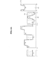
- FIG. 1 is a perspective view illustrating a thin film transistor substrate according to an exemplary embodiment of the present invention
- FIG. 2 is a sectional view illustrating the thin film transistor substrate cur away along "I-I", “II-II” and "III-III" lines of FIG. 1 ;
- FIGS. 3A and 3B are perspective and sectional views to illustrate a method for fabricating the thin film transistor substrate having a multi-stepped structure in detail
- FIGS. 4A and 4C are sectional views to illustrate a method for fabricating the thin film transistor substrate having a multi-stepped structure in detail
- FIGS. 5A and 5B are perspective and sectional views to illustrate a method for fabricating a first conductor pattern group of the thin film transistor according to the above embodiment of the present invention
- FIGS. 6A to 6C are sectional views to illustrate a method for fabricating a first conductor pattern group of the thin film transistor according to the above embodiment of the present invention
- FIGS. 7A and 7B are perspective and sectional views to illustrate a method for fabricating a semiconductor layer of the thin film transistor substrate according to the embodiment of the present invention
- FIGS. 8A to 8D are sectional views to illustrate a method for fabricating the semiconductor layer of the thin film transistor substrate according to the embodiment of the present invention.
- FIGS. 9A and 9B are perspective and sectional views to illustrate a method for fabricating a second conductor group of the thin film transistor substrate according to the embodiment of the present invention.
- FIGS. 10A to 10E are sectional views to illustrate a method for fabricating the second conductor group of the thin film transistor substrate according to the embodiment of the present invention.
- FIGS. 11A and 11B are perspective and sectional views to illustrate a process of removing a gate insulator layer and an active layer provided on a gate pad of the thin film transistor substrate according to the above embodiment of the present invention
- FIGS. 12A to 12D are sectional views to illustrate the process of removing the gate insulator layer and the active layer provided on the gate pad of the thin film transistor substrate according to the above embodiment of the present invention
- FIG. 13 is a sectional view illustrating a thin film transistor substrate according to another embodiment of the present invention.
- FIGS. 14A to 14I are sectional views to illustrate a method for fabricating the thin film transistor substrate shown in FIG. 13 ;
- FIG. 15 is a sectional view illustrating a flat display device having the thin film transistor substrate applied thereto.
- FIGS. 1 and 2 are a perspective view and a sectional view illustrating a thin film transistor substrate according to an exemplary embodiment of the present invention.
- the thin film transistor substrate shown in FIGS. 1 and 2 includes a substrate 101, gate lines 102 and data lines 104 alternatively formed on the substrate 101, with a gate insulator layer 112 provided there between, and a thin film transistor 130 adjacent to a cross portion of two gate and data lines.
- a thin film transistor substrate includes a gate pad 150 joined to the gate line 102 and a data pad 160 joined to the data line 104.
- the substrate 101 has first to fifth horizontal surfaces (T1, T2, T3, T4 and T5) having gradually increasing heights and it forms a multi-stepped structure.
- the first horizontal surface (T1) is exposed by a first groove (101a) having a first depth (d1).
- the second horizontal surface (T2) is exposed by a second groove (101b) having a second depth lower than the first depth (d1).
- the third horizontal surface (T3) is exposed by a third groove 101c having a third depth (d3) lower than the second depth (d2).
- the fourth horizontal surface (T4) is exposed by a fourth groove 101d having a fourth depth (d4) lower than the third depth (d3).
- the first horizontal surface (T1) is located between neighboring two pixel areas to separate channels of the pixel areas from each other. That is, the first horizontal surface (T1) is formed in a predetermined area corresponding to gate lines located in both opposite sides of a data line located between the gate lines. Active layers 114 are not formed in the first groove 101a of the first horizontal surface (T1) and the channels of the neighboring pixel areas are separated.
- the third horizontal surface (T3) is corresponding to a cross area of the gate and data lines 102 and 104.
- the fifth horizontal surface (T5) is corresponding to an area having the largest height of the substrate 101, except the areas corresponding to the first to fourth horizontal surfaces (T1, T2, T3 and T4). Especially, a taper angle of the fifth horizontal surface (T5) may be adjusted based on close horizontal surfaces to prevent short circuit between the data line 104 and a drain electrode 110 and between a source electrode 108 and the drain electrode 110.
- a taper angle ( ⁇ 1) of the side surface located between the second horizontal surface (T2) in which a gate electrode 106 and the gate line 102 formed and the fifth horizontal surface (T5) adjacent to the second horizontal surface (T2) may be larger than a taper angle ( ⁇ 2) of the side surface located between the fourth horizontal surface (T4) in which the source and drain electrodes 108 and 110 are formed and the second horizontal surface (T2) in which the gate electrode 106 is formed. Because of that, the source and drain electrodes 108 and 110 and the data line 104 may not be extended to the fifth horizontal surface (T5) and the sides surfaces located between the second horizontal surface (T2) adjacent to the fifth horizontal surface (T5) and neighboring fifth horizontal surface (T5), such that the short circuit between them may be prevented.
- Such the substrate 101 may be formed of plastic film made of at least one organic material selected out of Polyethylene Naphthalate (PEN), Polyethylene Terephthalate (PET), Polyethylene Ether Phathlate, Polycarbonate, Polyimide and Polyacrylate.
- PEN Polyethylene Naphthalate
- PET Polyethylene Terephthalate
- PET Polyethylene Ether Phathlate
- Polycarbonate Polyimide
- Polyacrylate any organic material selected out of Polyethylene Naphthalate (PEN), Polyethylene Terephthalate (PET), Polyethylene Ether Phathlate, Polycarbonate, Polyimide and Polyacrylate.
- the thin film transistor 130 is formed in the second groove 101b of the substrate and it includes the gate electrode 106, the source electrode 108, the drain electrode 110, the active layer 114 and an ohmic contact layer 116.
- the gate electrode 106 is joined to the gate line 102 and the source electrode 108 is joined to the data line 104.
- the drain electrode 110 is opposed to the source electrode 108 and the active layer 114 is overlapped with the gate electrode 106, with the gate insulator layer 112 located there between, to form a channel between the source electrode 108 and the drain electrode 110.
- the ohmic contact layer 116 is formed on a predetermined area of the active layer 114 except the channel area, to ohmic-contact with the source and drain electrodes 108 and 110.
- the gate electrode 106 is joined to the gate line 102 and it is formed on the first to third horizontal surfaces (T1, T2 and T3) of the substrate 101 and the side surfaces located between two of them.
- the source electrode 108 is formed on the fourth horizontal surface (T4) of the substrate 101 and the side surfaces located between two of the second to fourth horizontal surfaces, to be joined to the data line 104.
- the drain electrode 110 is formed on the fourth horizontal surface (T4) of the substrate 101 and the side surfaces located between two of the second to fourth horizontal surfaces (T2, T3 and T4), to be opposed to the source electrode 108.
- the active layer 114 is formed on the first horizontal surface (T1) of the substrate and the side surfaces located between the first and second horizontal surfaces (T1 and T2), along the gate line 102 and the gate electrode 106.
- Such the active layer 114 is formed overlapping with the gate electrode 106, having the gate insulator layer 112 located there between, and it forms the channel between the source electrode 108 and the drain electrode 110.
- the active layer 114 is separated from another active layer of a neighboring pixel area by the first groove 101a formed in both sides of the data line 104.
- the ohmic contact layers 116 may be formed between the source electrode 108 and the drain electrode 110 and between each data line 104 and the active layer 114, respectively. Especially, the ohmic contact layer 116 is formed on the active layer 114, except the channel area, to ohmic-contact with the source electrode 108 and the drain electrode 110.
- the gate line 102 is formed in the first and second grooves 101a and 101b of the substrate 101 and it is joined with a gate driver (not shown) via the gate pad 150.
- the data pad 150 is formed in the second groove 101b having the second depth (d2) formed in the substrate, with extended from the gate line 102 on the second horizontal surface (T2).
- the gate insulator layer 112 is not formed on such the gate pad 150 and the gate pad 150 is exposed outside accordingly.
- the data lines 104 are formed in the third and fourth grooves 101c and 101d of the substrate and it is joined with a data driver (not shown) via the data pad 160.
- the data pad 160 is formed in the fourth groove 101d, with extended from the data line 104 on the fourth horizontal surface (T4) of the substrate 101.
- FIGS. 1 and 2 a method for fabricating the thin film transistor substrate according to the present invention shown in FIGS. 1 and 2 will be described.
- FIGS. 3A and 3B are perspective and sectional views to explain a fabricating process of the substrate having multi-steps provided in the thin film transistor substrate.
- the substrate 101 having the first to fifth horizontal surfaces (T1, T2, T3, T4 and T5) located with different heights, respectively, may be provided.
- the first horizontal surface (T1) is exposed via the first groove (101a) having the first depth (d1) and the second horizontal surface (T2) is exposed via the second groove 101b having the second depth (d2) lower than the first depth (d1).
- the third horizontal surface (T3) is exposed via the third groove 101c having the third depth (d3) lower than the second depth (d2) and the fourth horizontal surface is exposed via the fourth groove 101d having the fourth depth (d4) lower than the third depth (d3).
- the fifth horizontal surface (T5) is located at the highest position of the substrate 101 higher than the fourth horizontal surface (T4).
- the taper angle ( ⁇ 1) of the side surface exposed between the second horizontal surface (T2) of the substrate 101 is larger than the taper angle ( ⁇ 2) of the side surface exposed between the second horizontal surface (T2) and the fourth horizontal surface (T4).
- an imprint-mold 200 having a plurality of projections 200a, 200b, 200c and 200d may be aligned on a plastic film 100.
- the imprint-mold 200 includes first to fourth projections 200a, 200b, 200c and 200d having sequentially lowered heights, respectively.
- the first projection 200a has a predetermined first height, corresponding to the area located in the neighboring pixel area in which the active layer forming the channel of the thin film transistor is separated.
- the second projection 200b has a second height lower than the first height, corresponding to the area in which the first conductor pattern group having the gate electrode and the gate pad will be formed.
- the third projection 200c has a third height lower than the second height, corresponding to the crossed area between the data line and the gate line.
- the fourth projection 200d has a predetermined height lower than the third height, corresponding to the area in which the second conductor group having the data line, the source electrode, the drain electrode and the data pad will be formed.
- Such the imprint-mold 200 may be made of rubber material having high elasticity, for example, Poly Dimethyl Siloxane (PDMS) and the like.
- PDMS Poly Dimethyl Siloxane
- the first to fourth grooves 101a, 101b, 101c and 101d having reversal-transferred patterns of the first to fourth projections 200a, 200b, 200c and 200d and the substrate 101 having the first to fifth horizontal surfaces T1, T2, T3, T4 and T5.
- the first groove 101a has the first depth (d1) corresponding to the height of the first projected pattern 200a of the imprint-mold 200
- the second groove 101b has the second depth (d2, de ⁇ d1) corresponding to the height of the second projected pattern 200b.
- the third groove 101c has the third depth (d3, d3 ⁇ d2) corresponding to the height of the third projected pattern 200c of the imprint-mold 200 and the fourth groove 101d has the fourth depth (d4, d4 ⁇ d3) corresponding to the height of the fourth projected pattern 200d of the imprint-mold 200.
- the taper angle ( ⁇ 1) of the side surface exposed between the second horizontal surface (T2) and the fifth horizontal surface (T5) may be larger than the taper angle ( ⁇ 2) of the side surface exposed between the second horizontal surface (T2) and the fourth horizontal surface (T4).
- FIGS. 5A and 5B are perspective and sectional views to explain a fabricating process of the first conductor pattern group of the thin film transistor substrate according to the present invention.
- the first conductor pattern group including the gate line 102, the gate electrode 106 and the gate pad 150 is formed on the first to third horizontal surfaces (T1, T2 and T3) and the side surfaces located between each two of the horizontal surfaces.
- a gate metal layer 172 and a first etch resist are sequentially formed on a top surface of the substrate 101.
- the gate metal layer 172 is formed of aluminum, copper or molybdenum and the first etch resist is formed of acrylic resin or novolac resin which have tolerance to etchant of the gate metal layer.
- the first etch resist is ashed in a plasma ashing process, under an atmospheric pressure or vacuum state and a first etch resist pattern 170 is formed.
- Gas mixture of 02, NF3, SF3, N2, Clean dry air (CDA) is used as ashing gas.
- the first etch resist pattern 170 is removed from the fourth and fifth horizontal surfaces (T4 and T5) of the substrate, with formed on the first to third horizontal surfaces (T1 ⁇ T3) and on the side surfaces located between each two of the first to third horizontal surfaces.
- the gate metal layer 172 is etched by using the first etch resist pattern 170 as mask. Because of that, the first conductor pattern group including the gate line 102, the gate electrode 106 and the gate pad 150 is formed as shown in FIG. 6B .
- the first conductor pattern group is formed on each of the first to third horizontal surfaces (T1 ⁇ T3) and on the side surfaces located on each two of the first to third horizontal surfaces.
- the first etch resist pattern 170 remaining on the first conductor pattern group is removed in a strip process.
- FIGS. 7A and 7B are a perspective view and a sectional view to explain a method for fabricating the gate insulator layer, the active layer and the ohmic contact layer on the thin film transistor substrate according to the present invention.
- the ohmic contact layer is not shown in FIG. 7A
- the ommic contact layer is formed in the same pattern of the active layer as shown in FIG. 7B .
- the gate insulator layer 112 is formed on a top surface of the substrate 101 having the first conductor pattern group formed thereon.
- the active layer 114 and the ohmic contact layer 116 are formed on the second horizontal surface T2 and the side surfaces located between the second and third horizontal surfaces T2 and T3, with the same patterns.
- the height of the active layer 114 formed on the side surface located between the second and third horizontal surfaces may be lower than the height of the gate electrode 106 formed between the side surface located between the second and third horizontal surfaces.
- the gate insulator layer 112 and the second etch resist are sequentially layered on the surface of the substrate 101 having the first conductor pattern group formed thereon.
- a second etch resist is ashed in the plasma ashing process, under the atmospheric pressure or vacuum state, and a second etch resist pattern 184 is then formed.
- gas mixture of 02, NF3, SF3, N2 and CDA is sued as ashing gas.
- the second etch resist pattern 184 is removed from the second to fifth horizontal surfaces T2, T3, T4 and T5 and the side surfaces located between each two of them, only to remain on the first horizontal surface T1.
- the second etch resist pattern 184 is formed on front and side surfaces of the gate insulator layer 112 formed on the first horizontal surface T1, with a predetermined thickness to be level with the gate insulator layer 112 formed on the second horizontal surface T2.
- An amorphous silicon layer 182 having impurity (n+ or p+) doped thereon and an intrinsic amorphous silicon layer 192 is layered on the substrate 101 having such the second etch resist pattern 184 formed thereon.
- the second etch resist pattern 184 and the amorphous silicon layer 182 and the amorphous silicon layer 192 having the impurity (n+ or p+) doped thereon, which are formed on the second etch resist pattern 184, may be removed together in a lift-off process.
- the impurity (n+ or p+) doped amorphous silicon layer 192 formed on the gate insulator layer 112 on the first horizontal surface T1 of the substrate 101 may be patterned to be removed, and then the active layer 114 and the ohmic contact layer 116 are formed.
- a semiconductor layer including the active layers 114 configured to form channels of neighboring pixels are separated from a semiconductor layer including the ohmic contact layers 116 for ohmic-contact, with the data lines 104 located there between.
- semiconductor layers 114 and 116 formed in cross areas of the gate and data lines 102 and 104 may be separated from semiconductor layers 114 and 116 formed on the gate lines 102 located right and left sides of the semiconductor layers 114 and 116, to be formed in an island shape.
- a third etch resist is layered on the substrate 101 having the semiconductor layers 114 and 116 formed thereon.
- the first etch resist may be acrylic resin or novolac resin having tolerance to the etchant of the semiconductor layer.
- the third etch resist is ashed in the plasma ashing process, under the atmospheric pressure or vacuum state, and a third etch resist pattern 180 is then formed. Gas mixture of 02, NF3, N2 and CDA is used as ashing gas.
- the third etch resist pattern 180 is formed on to the third to fifth horizontal surfaces T3, T4 and T5 and the side surfaces located between each two of them, to be removed.
- the third etch resist pattern 180 is used as mask in etching the semiconductor layer 114 and 116 as shown in FIG. 8C . After that, the semiconductor layers 114 and 116 may be formed on the second horizontal surfaces T2 and the side surfaces located between the second and third horizontal surfaces T2 and T3. As shown in FIG. 8D , the third etch resist pattern 180 remaining on the semiconductor layers 114 and 116 may be removed in the strip process.
- FIGS. 9A and 9B are a perspective view and a sectional view to explain a method for fabricating the second conductor pattern group and the ohmic contact layer.
- the second conductor pattern group including the source electrode 108, the drain electrode 110, the data line 104 and the data pad 160 is formed on the third and fourth horizontal surfaces T3 and T4, the side surfaces located between the two horizontal surfaces and the side surface located between the second and third horizontal surfaces.
- the source electrode 108 and the drain electrode 110 are partially formed on the side surface located between the second and third horizontal surfaces T2 and T3, to be overlapped with the gate electrode 106 and the active layer 114.
- the etch resist is coated and ashed on the substrate 101, and then the etch resist pattern to partially expose an end of the ohmic contact layer 116 is formed.
- the third etch resist pattern 180 remaining on the active layer 114 shown in FIG. 8C is ashed, not removed in the strip process.
- the method of patterning by using the third etch resist pattern 180 shown in FIG. 8C will be described. That is, the third etch resist pattern 180 is ashed and it is formed to expose a predetermined part of the end of the ohmic contact layer 116 located on the side surface between the second and third horizontal surfaces T2 and T3.
- a source/drain metal layer 194 and a fourth etch resist may be sequentially formed on a front surface of the substrate 101 having the third etch resist pattern 180 formed thereon.
- the fourth etch resist is formed of acrylic resin or novolac resin having tolerance to etchant of the source/drain metal layer.
- the fourth etch resist is ashed in the plasma ashing process, under the atmospheric pressure or vacuum state, and a fourth etch resist pattern 196 is then formed. Gas mixture of 02, NF3, SF3, N2 and CDA is used as ashing gas.
- the fourth etch resist pattern 196 is removed from the fifth horizontal surface T5 and the side surface located between the fourth and fifth horizontal surfaces T4 and T5, to remain the other area of the substrate 101.
- the source/drain metal layer 194 is etched by using the fourth etch resist pattern 196 as mask. Because of that, the second conductor pattern group including the source and drain electrodes 108 and 110, the data line 104 and the data pad 160 may be formed, each of them connected with each other. As shown in FIG. 10d , the fourth etch resist pattern 196 remaining on the second conductor pattern group is removed in the strip process. After that, the third etch resist pattern 180 and the source and drain electrodes are removed together in the lift-off process, to separate the source and drain electrodes 108 and 110.
- the ohmic contact layer 116 located between the source and drain electrodes 108 and 110 is removed in an etching process using the source and drain electrodes 108 and 110 as mask, to expose the active layer 114 and to remove the ohmic contact layer 116 not overlapped with the active layer 114 on the gate pad 150 and the gate line 102.
- the third conductor pattern group is not formed on the side surface located between the second and fifth horizontal surfaces T2 and T5 to prevent short circuit generated between the source and drain electrodes 108 and 110 and between the source electrode 108 and the data line 104.
- a first taper angle ( ⁇ 1) between the second horizontal surface T2 and the side surface located between the second horizontal surface and the neighboring fifth horizontal surface T5 may be larger than a second taper angle ( ⁇ 2) between the other side surfaces.
- the source/drain metal layer 194 would be formed with a relatively smaller thickness, compared with the other area of the substrate.
- the source/drain metal layer 194 located on the side surface between the second and fifth horizontal surfaces T2 and T5, corresponding to the first taper angle ( ⁇ 1) has a higher etching rate than the source/drain metal layer 194 located on the side surfaces corresponding to the second taper angle.
- the etchant infiltration velocity to the side surface located between the second and fifth horizontal surfaces T2 and T5 corresponding to the first taper angle ( ⁇ 1) is higher than the etchant infiltration velocity to the other area.
- the etching rate of the source/drain metal layer 194 located on the side surface between the second and fifth horizontal surface T2 and T5 corresponding to the taper angle ( ⁇ 1) is higher.
- the source/drain metal layer 194 located in the side surface between the second and fifth horizontal surfaces T2 and T5 corresponding to the first taper angle ( ⁇ 1) may be removed completely.
- the source/drain metal layer 194 on the fourth horizontal surface T4 is also etched, except the side surface between the second and fifth horizontal surfaces T2 and T5 corresponding to the first taper angle ( ⁇ 1), and the area of the fourth horizontal surface T4 is relatively large enough not to affect the pattern representation.
- FIGS. 11A and 11B are a perspective view and a sectional view to explain a removing process of the gate insulator layer and active layer on the gate pad of the thin film transistor substrate.
- the gate insulator layer 112 and the active layer 114 on the gate pad 150 are removed to expose the gate pad 150.
- a fifth etch resist 136 is formed on a front surface of the substrate 101 having the second conductor pattern group formed thereon.
- the fifth etch resist 136 is formed of acrylic resin or novolac resin having tolerance to the etchant of the gate insulator layer 112 and the active layer 114. after that, a predetermined area formed on the substrate corresponding to the gate pad 150 is selectively dipped in a bath receiving strip liquid and the fifth etch resist 136 of the area corresponding to the gate pad 150 is selectively removed.
- the fifth etch resist pattern 134 to expose the area corresponding to the gate pad 150 is formed as shown in FIG. 12c .
- the exposed active layer and gate insulator layer 112 are etched by using the fifth etch resist pattern 134 as mask. After that, the active layer 114 and the gate insulator layer 112 formed on the gate pad 150 are removed and the gate pad 150 is exposed outside as shown in FIG. 12d . Also, the gate insulator layer 112 located between the gate pads 150 is removed and the fifth horizontal surface T5 of the substrate 101 is exposed.
- FIG. 13 is a sectional view of a thin film transistor substrate according to another embodiment (second embodiment) of the present invention.
- a thin film transistor substrate shown in FIG. 13 includes the same elements except an ohmic contact layer formed under a second conductor pattern group in the same pattern. Because of that, description of the same elements will be omitted.
- the ohmic contact layer 116 is formed on the active layer 114 except a channel area to ohmic-contact with the source electrode 108 and the drain electrode 110. Such the ohmic contact layer 116 is formed under the source and drain electrode 108 and 110 and the data line and pad 104 and 160, with the same pattern as they have. In other words, the ohmic contact layer 116 is formed together with the third conductor pattern group including the source electrode 108, the drain electrode 110, the data line 104 and the data pad 160 simultaneously.
- FIGS. 14a and 14i are sectional views to explain a method for fabricating the thin film transistor substrate shown in FIG. 13 .
- a substrate having a multi-step structure is provided according to the fabricating method shown in FIGS. 4A to 4C .
- the first conductor pattern group is formed according to the fabricating method shown in FIGS. 6A to 6C .
- the gate insulator layer 112 and the second etch resist are sequentially layered on a front surface of the substrate 101 having the first conductor pattern group formed thereon.
- the second etch resist is ashed and the second etch resist pattern 184 is formed.
- the amorphous silicon layer 182 is layered on the substrate 101 having such the second etch resist pattern 184 formed thereon.
- the second etch resist pattern 184 and the amorphous silicon layer 182 on the second etch resist pattern are removed together.
- the amorphous silicon layer 182 formed on the gate insulator layer 112 located on the first horizontal surface T1 of the substrate is patterned to be removed as shown in FIG. 14B , and then the active layer 114 is formed.
- the third etch resist is layered and ashed on the substrate 101 having the active layer 114 formed thereon, and then the third etch resist pattern 180 is formed.
- the active layer 114 is etched by using the third etch resist pattern 180 as mask. Then, after the third etch resist pattern 180 remaining on the active layer 114 shown in FIG.
- the amorphous silicon layer 192 having the impurity (n+ or p+) doped thereon or intrinsic, the source/drain metal layer 194 and the fourth etch resist are sequentially formed on the front surface of the substrate 101 having the ashed third etch resist pattern 180 formed thereon, as shown in FIG. 14E .
- the fourth etch resist is ashed and the fourth etch resist pattern 196 is formed.
- the source/drain metal layer 194 and the amorphous silicon layer 192 having the impurity doped thereon are sequentially etched by using the fourth etch resist pattern 196 as mask, and then the second conductor pattern group including the source and drain electrodes 108 and 110, the data line 104 and the data pad 160, which are connected with each other, and the ohmic contact layer 116 located under the second conductor pattern group may be formed as shown in FIG. 14F . After that, as shown in FIG. 14G , the fourth etch resist pattern 196 remaining on the second conductor pattern group is removed in the strip process.
- the third etch resist pattern 180, the ohmic contact layer located on the third etch resist pattern 180 and the source and drain electrodes are removed together in the lift-off process.
- the source and drain electrodes 108 and 110 are separated.
- the ohmic contact layer 116 located between the source and drain electrodes 108 and 110 is removed to expose the active layer 114.
- the ohmic contact layer 116 is removed in a fabricating process shown in FIGS. 12A and 12D .
- FIG. 15 is a sectional view illustrating an organic electro luminescent display device the thin film transistor substrate is applied to according to the present invention.
- the organic electro luminescent display device shown in FIG. 15 includes the thin film transistor substrate according to the present invention, a luminescent substrate 210 and a contact spacer 202 to connect the others with each other.
- the luminescent substrate 210 includes first electrodes 204, an organic electro luminescent layer 206 and second electrodes 208, which are formed on a second substrate 111 sequentially.
- the first electrode is formed of transparent conductive material on the second substrate 111 made of transparent plastic material.
- an electron injection layer (EIL), an electron transport layer (ETL), a light emitting layer, a hole transport layer (HTL) and a hole injection layer (HIL) are multi-layered sequentially.
- the light emitting layer 206 full-emits a light having a specific wave toward the second substrate 111, with an exciter, generated when the electron of the first electrode 204 is re-bonded with the hole of the second electrode 208, returning to a bottom state.
- the second electrodes 208 are opposed to the first electrodes 204, with the organic electro luminescent layer 206 located between them.
- Such the second electrode made of opaque conductive material.
- the contact spacer 202 electrically joins the second electrodes 208 of the luminescent substrate 210 with the drain electrodes 110 of the thin film transistor substrate. That is, a driving signal is supplied to the second electrodes 208 from the data line 104 via the contact spacer 202.
- the plurality of such the contact spacers 202 are formed between the drain electrodes and the second electrodes 208.
- the drain electrodes 110 is employed as second electrodes 208 without the contact spacer 202 and the luminescent layer 206 and the first electrodes 204 are multilayered on the drain electrodes 110 sequentially.
- the drain electrodes 110 are employed as second electrodes 208 without the contact spacer 202. Because of that, increase of an overall thickness and weight generated by the height of the contact spacer 202 may be prevented, to allow the display device to be compact and thin.
- the thin film transistor substrate according to the present invention is applied to the organic electro luminescent display device.
- the thin film transistor substrate according to the present invention may be applied to an electronic ink type display device and a reflection type liquid display device. That is, if it is applied to the electronic ink type display device, the thin film transistor substrate according to the present invention is joined with an electronic ink film via the contact spacer 202 or the drain electrodes 110 is employed as driving electrode of the electronic ink type display device.
- the drain electrodes 110 formed in the pixel areas provided in the cross portions of the gate lines 102 and the data lines are used as reflection electrodes to drive the liquid.
Abstract
Description
- This application claims the benefit of the Patent Korean Application No.
10-2010-0055514, filed on June 11, 2010 - The present invention relates to a thin film transistor substrate having a self-alignment function to reduce production cost accordingly and a method of fabricating the thin film transistor, and a flat display having the thin film transistor substrate.
- In recent, a display device market has been changing rapidly, focused on flat display devices efficient to apply an enlarge size and a compact size to. Such a flat display device may be classified into a liquid crystal display (LCD), a plasma display panel (PDP), an organic electro luminescence display (OLED) and the like. The flat display device uses a glass substrate as supporting body configured to support a plurality of fin films. The glass substrate has limitation of lessened thickness. Even if the thickness of the glass substrate is lessened, the glass substrate has a disadvantage of easily-breakable because it has no durability and flexibility.
- As a result, flexible displays have been emerging in the market which uses material having a thin thickness and durability, for example, plastic instead of glass substrate having no durability and flexibility.
- Compared with the glass substrate, it is easy to change a shape of a plastic film used in such a flexible display because of heat, tension, chemical reaction and moisture absorption and the like. Because of that, an exterior appearance of the flexible substrate has to be put into consideration in each assembly line disadvantageously. Especially, the plastic film happens to be thermal-contractible by 200ppm at 150°C. If a flexible display is fabricated, using such the plastic film, accuracy of thin-film-inter-layer alignment would deteriorate seriously.
- To solve this problem,
US Patent No. 7,202,179 and No.7,521,313 disclose a thin film device having self aligned imprint lithography. - Specifically, according to
USP No.7,202,179 , a plurality thin film device layers are deposited on a substrate and an imprinted 3D template structure, such as an imprinted polymer, is then provided on the plurality of thin film device layers. After that, the plurality of thin film device layers and the 3D template structure are etched. This etching forms a rudimentary structure for a thin film device. That is, the formed plurality of thin film device layers is patterned by using multi-stepped resist as mask through a plurality of ashing and etching processes. In this case, a problem of multi-layer alignment may be solved because the multi-stepped resist is used in patterning the plurality of thin film device layers. However, undercutting is used to pattern a gate layer which is the lowest layer. Here, it is difficult to perform an undercut process and there is limitation of forming a pattern shape. Also, a gate dielectric layer provided on the gate layer might be floating because of the undercut structure and product reliability would deteriorate accordingly. - According to
USP No.7,512,313 , when forming a pattern in an exposed area of a substrate having at least one step, exposed area is treated to provide at least one etch resist area of material. However, the material the surface treating process is applied to is limited and it is difficult to secure that kind of material. Also, the surface treating process is additionally provided and the overall assembly process has to be complicated accordingly. - Accordingly, the present invention is directed to a thin film transistor substrate and a method for fabricating the same.
- An object of the present invention is to provide a thin film transistor substrate capable of performing self alignment and a method for fabricating the same, and a method for fabricating the same.
- Additional advantages, objects, and features of the disclosure will be set forth in part in the description which follows and in part will become apparent to those having ordinary skill in the art upon examination of the following or may be learned from practice of the invention. The objectives and other advantages of the invention may be realized and attained by the structure particularly pointed out in the written description and claims hereof as well as the appended drawings.
- To achieve these objects and other advantages and in accordance with the purpose of the invention, as embodied and broadly described herein, a thin film transistor substrate includes a substrate comprising a plurality of grooves having different depths, respectively, to have a multi-step structure; gate and data lines alternatively crossed in the grooves to form a plurality of pixel areas; thin film transistors formed in the grooves of the substrate to be formed in cross portion of the gate and data lines, wherein active layers of the thin transistors are formed along the gate lines and gate electrodes, the active layers separated from active layers of neighboring pixel areas with the data line located there between.
- The substrate may include first to fourth grooves having different heights, respectively, and a first horizontal surface of the substrate may be exposed by the first groove and a second horizontal surface of the substrate may be exposed by the second groove having a lower depth than the first groove and a third horizontal surface of the substrate may be exposed by the third groove having a lower depth than the second groove and a fourth horizontal surface of the substrate may be exposed by the fourth groove having a lower depth than the third groove.
- The thin film transistor may include gate electrodes formed on the first and second horizontal surfaces and side surfaces located between each two of the first to third horizontal surfaces; a gate insulator layer formed on a front surface of the substrate; source and drain electrodes formed on the first and fourth horizontal surfaces of the substrate and on the gate insulator layer corresponding to side surfaces located between each two of the second to fourth horizontal surfaces; the active layers formed on the second horizontal surface of the substrate and on the gate insulator layer corresponding to a side surface located between the second and third horizontal surfaces, the active layer overlapped with the gate electrodes with the gate insulator layer located there between to form channels between the source and drain electrodes; and an ohmic contact layer formed between each of the source and drain electrodes and the active layer.
- The active layers may be separated from active layers of neighboring pixel areas by the first groove located in both sides of the data lines.
- The gate and data lines may be crossed on the third horizontal surface of the substrate, with the gate insulator layer located there between.
- A taper angle of a side surface located between the fourth horizontal surface having the source and drain electrodes formed thereon and second horizontal surface having the gate electrodes formed thereon may be smaller than a taper angle of a side surface located between the second horizontal surface having the gate electrodes and gate lines formed thereon and the fifth horizontal surface adjacent to the second horizontal surface.
- The thin film transistor substrate may further include a gate pad joined with the gate lines, the gate pad formed on the second horizontal surface; and a data pad joined with the data lines, the data pad formed on the fifth horizontal surface, wherein the gate insulator layer and the active layer are formed to expose the gate pad.
- In another aspect of the present invention, a method for fabricating a thin film transistor substrate comprising steps of: forming a substrate comprising a plurality of grooves having different depths, respectively, to have a multi-step structure; and forming gate and data lines, alternatively crossed to form a plurality of pixel areas, and thin film transistors, formed in cross portions of the gate and data lines, in the grooves of the substrate; wherein active layers of the thin transistor are formed along the gate lines and gate electrodes, the active layers separated from active layers of neighboring pixel areas having the data line located there between.
- The step of forming the substrate may include steps of: forming an imprint-mold comprising first to fourth projections corresponding to the first to fourth grooves; forming the substrate having the first to fourth grooves by pressing a plastic film, using the imprint-mold; and separating the imprint-mold from the substrate.
- The step of forming the gate and data lines and the thin film transistors in the grooves of the substrate may include steps of: forming the gate lines and gate electrodes of the thin film transistors on the first and second horizontal surfaces and on side surfaces located between each two of the first to third horizontal surfaces; forming a gate insulator layer on a front surface of the substrate; forming the active layers on the second horizontal surface of the substrate and on the gate insulator layer corresponding to a side surface located between the second and third horizontal surfaces, the active layers overlapped with the gate electrodes with the gate insulator layer located there between to form channels between the source and drain electrodes; and forming source electrodes, drain electrodes and data lines on the third and fourth horizontal surfaces of the substrate and one side surfaces located between each two of the second to fourth horizontal surfaces.
- The step of forming the gate lines and the gate electrodes of the thin transistors may include steps of: forming a gate metal layer on a front surface of the substrate; forming first etch resist patterns on the first to third horizontal surfaces and on side surfaces located each two of the first to third horizontal surfaces; etching the gate metal layer by using the first etch resist patterns as mask; and removing the first etch resist patterns.
- The step of forming the active layers according to an embodiment may include steps of: forming a second etch resist pattern on the first horizontal surface of the substrate having the gate insulator layer formed thereon; forming first and second silicon layers on the substrate having the second etch resist pattern formed thereon; removing the second etch resist pattern, the first and second silicon layers on the second etch resist pattern in a lift-off process; forming a third etch resist pattern to cover the first and second horizontal surfaces and the side surface located between each two of the first to third horizontal surfaces; and forming the active layers and an ohmic contact layer on the active layers by etching the first silicon layer, using the third etch resist pattern as mask.
- The step of forming the active layers according to another embodiment may include steps of: forming a second etch resist pattern on the first horizontal surface of the substrate having the gate insulator layer formed thereon; forming a first silicon layer on the substrate having the second etch resist pattern formed thereon; removing the second etch resist pattern and the first silicon layer on the second etch resist pattern in a lift-off process; forming a third etch resist pattern to cover the first and second horizontal surfaces and side surfaces located each two of the first to third horizontal surfaces; and forming the active layers by etching the first silicon layer, using the third etch resist pattern as mask.
- The step of forming the data lines, the source electrodes and the drain electrodes may include steps of: ashing the third etch resist pattern to expose an end of the ohmic contact layer partially; forming a source/drain metal layer on the substrate to cover the ashed third etch resist pattern; forming a fourth etch resist pattern on the first to fourth horizontal surfaces on the source/drain metal layer; etching the source/drain metal layer, using the fourth etch resist pattern as mask; removing the fourth etch resist pattern; and removing the third etch resist pattern and the source/drain metal layer on the third etch resist pattern in a lift-off process.
- The step of forming the data lines, the source electrodes and the drain electrodes according to another embodiment may include steps of: ashing the third etch resist pattern to expose an end of the active layer partially; forming a second silicon layer and a source/drain metal layer on the substrate to cover the ashed third etch resist pattern; forming a fourth etch resist pattern on the first to fourth horizontal surfaces formed on the source/drain metal layer; forming an ohmic contact layer together with the data lines and the source and drain electrodes by sequentially etching the source/drain metal layer and the second silicon layer, using the fourth etch resist pattern as mask; removing the fourth etch resist pattern; and separating the source and drain electrodes and the ohmic contact layer located between the source and drain electrodes by removing the third etch resist pattern in a lift-off process.
- Here, the second etch resist pattern may be level with respect to the gate insulator formed on the second horizontal surface.
- The method may further include steps of: forming gate pads on the second horizontal surface, together with the gate lines; forming data pads on the fourth horizontal surface, together with the data lines; and exposing the gate pads by removing the active layer and the gate insulator layer formed on the gate pads.
- Specifically, the step of exposing the gate pads may include steps of: coating etch resist on the front surface of the substrate having the source electrodes, the drain electrodes, the data lines and the data pads formed thereon; forming a fifth etch resist pattern by patterning the etch resist after dipping a predetermined portion of the substrate having the gate pads formed thereon; and etching the active layer and the gate insulator layer, using the fifth etch resist pattern as mask.
In a further aspect of the present invention, a flat panel display device includes a thin film transistor substrate; an array substrate opposed to the thin film transistor substrate, the array substrate comprising driving electrodes; and a contact spacer formed between the thin film transistor substrate and the array substrate, to join thin transistors with the driving electrodes, wherein the thin film substrate includes a substrate comprising a plurality of grooves having different depths, respectively, to have a multi-step structure; gate and data lines alternatively crossed in the grooves to form a plurality of pixel areas; thin film transistors formed in the grooves of the substrate to be formed in cross portion of the gate and data lines, wherein active layers of the thin transistors are formed along the gate lines and gate electrodes, the active layers separated from active layers of neighboring pixel areas with the data line located there between. - According to the present invention, the substrate including the plurality of the grooves having different depths, respectively, may be provided and a thin film patterns are formed in the grooves of the substrate. Because of that, a structure allowing a broad area may be designable and it is advantageous to apply a resist printing process to the present invention. Also, the thin film may be formed without an alignment process according to the present invention. Because of that, self-alignment is possible. The thin film pattern according to the present invention is not formed in the undercut structure and its assembling process efficiency and reliability may be improved accordingly.
- It is to be understood that both the foregoing general description and the following detailed description of the present invention are exemplary and explanatory and are intended to provide further explanation of the invention as claimed.
- The accompanying drawings, which are included to provide a further understanding of the disclosure and are incorporated in and constitute a part of this application, illustrate embodiment(s) of the disclosure and together with the description serve to explain the principle of the disclosure.
- In the drawings:
-
FIG. 1 is a perspective view illustrating a thin film transistor substrate according to an exemplary embodiment of the present invention; -
FIG. 2 is a sectional view illustrating the thin film transistor substrate cur away along "I-I", "II-II" and "III-III" lines ofFIG. 1 ; -
FIGS. 3A and3B are perspective and sectional views to illustrate a method for fabricating the thin film transistor substrate having a multi-stepped structure in detail; -
FIGS. 4A and4C are sectional views to illustrate a method for fabricating the thin film transistor substrate having a multi-stepped structure in detail; -
FIGS. 5A and5B are perspective and sectional views to illustrate a method for fabricating a first conductor pattern group of the thin film transistor according to the above embodiment of the present invention; -
FIGS. 6A to 6C are sectional views to illustrate a method for fabricating a first conductor pattern group of the thin film transistor according to the above embodiment of the present invention; -
FIGS. 7A and7B are perspective and sectional views to illustrate a method for fabricating a semiconductor layer of the thin film transistor substrate according to the embodiment of the present invention; -
FIGS. 8A to 8D are sectional views to illustrate a method for fabricating the semiconductor layer of the thin film transistor substrate according to the embodiment of the present invention; -
FIGS. 9A and9B are perspective and sectional views to illustrate a method for fabricating a second conductor group of the thin film transistor substrate according to the embodiment of the present invention; -
FIGS. 10A to 10E are sectional views to illustrate a method for fabricating the second conductor group of the thin film transistor substrate according to the embodiment of the present invention; -
FIGS. 11A and11B are perspective and sectional views to illustrate a process of removing a gate insulator layer and an active layer provided on a gate pad of the thin film transistor substrate according to the above embodiment of the present invention; -
FIGS. 12A to 12D are sectional views to illustrate the process of removing the gate insulator layer and the active layer provided on the gate pad of the thin film transistor substrate according to the above embodiment of the present invention; -
FIG. 13 is a sectional view illustrating a thin film transistor substrate according to another embodiment of the present invention; -
FIGS. 14A to 14I are sectional views to illustrate a method for fabricating the thin film transistor substrate shown inFIG. 13 ; and -
FIG. 15 is a sectional view illustrating a flat display device having the thin film transistor substrate applied thereto. - Reference will now be made in detail to the specific embodiments of the present invention, examples of which are illustrated in the accompanying drawings. Wherever possible, the same reference numbers will be used throughout the drawings to refer to the same or like parts.
-
FIGS. 1 and2 are a perspective view and a sectional view illustrating a thin film transistor substrate according to an exemplary embodiment of the present invention. - The thin film transistor substrate shown in
FIGS. 1 and2 includes asubstrate 101,gate lines 102 anddata lines 104 alternatively formed on thesubstrate 101, with agate insulator layer 112 provided there between, and athin film transistor 130 adjacent to a cross portion of two gate and data lines. A thin film transistor substrate includes agate pad 150 joined to thegate line 102 and adata pad 160 joined to thedata line 104. - The
substrate 101 has first to fifth horizontal surfaces (T1, T2, T3, T4 and T5) having gradually increasing heights and it forms a multi-stepped structure. The first horizontal surface (T1) is exposed by a first groove (101a) having a first depth (d1). The second horizontal surface (T2) is exposed by a second groove (101b) having a second depth lower than the first depth (d1). The third horizontal surface (T3) is exposed by athird groove 101c having a third depth (d3) lower than the second depth (d2). The fourth horizontal surface (T4) is exposed by afourth groove 101d having a fourth depth (d4) lower than the third depth (d3). - Especially, the first horizontal surface (T1) is located between neighboring two pixel areas to separate channels of the pixel areas from each other. That is, the first horizontal surface (T1) is formed in a predetermined area corresponding to gate lines located in both opposite sides of a data line located between the gate lines.
Active layers 114 are not formed in thefirst groove 101a of the first horizontal surface (T1) and the channels of the neighboring pixel areas are separated. - The third horizontal surface (T3) is corresponding to a cross area of the gate and
data lines - The fifth horizontal surface (T5) is corresponding to an area having the largest height of the
substrate 101, except the areas corresponding to the first to fourth horizontal surfaces (T1, T2, T3 and T4). Especially, a taper angle of the fifth horizontal surface (T5) may be adjusted based on close horizontal surfaces to prevent short circuit between thedata line 104 and adrain electrode 110 and between asource electrode 108 and thedrain electrode 110. that is, a taper angle (θ1) of the side surface located between the second horizontal surface (T2) in which agate electrode 106 and thegate line 102 formed and the fifth horizontal surface (T5) adjacent to the second horizontal surface (T2) may be larger than a taper angle (θ2) of the side surface located between the fourth horizontal surface (T4) in which the source and drainelectrodes gate electrode 106 is formed. Because of that, the source and drainelectrodes data line 104 may not be extended to the fifth horizontal surface (T5) and the sides surfaces located between the second horizontal surface (T2) adjacent to the fifth horizontal surface (T5) and neighboring fifth horizontal surface (T5), such that the short circuit between them may be prevented. - Such the
substrate 101 may be formed of plastic film made of at least one organic material selected out of Polyethylene Naphthalate (PEN), Polyethylene Terephthalate (PET), Polyethylene Ether Phathlate, Polycarbonate, Polyimide and Polyacrylate. - The
thin film transistor 130 is formed in thesecond groove 101b of the substrate and it includes thegate electrode 106, thesource electrode 108, thedrain electrode 110, theactive layer 114 and anohmic contact layer 116. - The
gate electrode 106 is joined to thegate line 102 and thesource electrode 108 is joined to thedata line 104. thedrain electrode 110 is opposed to thesource electrode 108 and theactive layer 114 is overlapped with thegate electrode 106, with thegate insulator layer 112 located there between, to form a channel between thesource electrode 108 and thedrain electrode 110. Theohmic contact layer 116 is formed on a predetermined area of theactive layer 114 except the channel area, to ohmic-contact with the source and drainelectrodes - The
gate electrode 106 is joined to thegate line 102 and it is formed on the first to third horizontal surfaces (T1, T2 and T3) of thesubstrate 101 and the side surfaces located between two of them. Thesource electrode 108 is formed on the fourth horizontal surface (T4) of thesubstrate 101 and the side surfaces located between two of the second to fourth horizontal surfaces, to be joined to thedata line 104. thedrain electrode 110 is formed on the fourth horizontal surface (T4) of thesubstrate 101 and the side surfaces located between two of the second to fourth horizontal surfaces (T2, T3 and T4), to be opposed to thesource electrode 108. Theactive layer 114 is formed on the first horizontal surface (T1) of the substrate and the side surfaces located between the first and second horizontal surfaces (T1 and T2), along thegate line 102 and thegate electrode 106. Such theactive layer 114 is formed overlapping with thegate electrode 106, having thegate insulator layer 112 located there between, and it forms the channel between thesource electrode 108 and thedrain electrode 110. In addition, theactive layer 114 is separated from another active layer of a neighboring pixel area by thefirst groove 101a formed in both sides of thedata line 104. - The ohmic contact layers 116 may be formed between the
source electrode 108 and thedrain electrode 110 and between eachdata line 104 and theactive layer 114, respectively. Especially, theohmic contact layer 116 is formed on theactive layer 114, except the channel area, to ohmic-contact with thesource electrode 108 and thedrain electrode 110. - The
gate line 102 is formed in the first andsecond grooves substrate 101 and it is joined with a gate driver (not shown) via thegate pad 150. Thedata pad 150 is formed in thesecond groove 101b having the second depth (d2) formed in the substrate, with extended from thegate line 102 on the second horizontal surface (T2). Thegate insulator layer 112 is not formed on such thegate pad 150 and thegate pad 150 is exposed outside accordingly. - The data lines 104 are formed in the third and
fourth grooves data pad 160. Thedata pad 160 is formed in thefourth groove 101d, with extended from thedata line 104 on the fourth horizontal surface (T4) of thesubstrate 101. - As follows, a method for fabricating the thin film transistor substrate according to the present invention shown in
FIGS. 1 and2 will be described. -
FIGS. 3A and3B are perspective and sectional views to explain a fabricating process of the substrate having multi-steps provided in the thin film transistor substrate. - As shown in
FIGS. 3A and3B , thesubstrate 101 having the first to fifth horizontal surfaces (T1, T2, T3, T4 and T5) located with different heights, respectively, may be provided. The first horizontal surface (T1) is exposed via the first groove (101a) having the first depth (d1) and the second horizontal surface (T2) is exposed via thesecond groove 101b having the second depth (d2) lower than the first depth (d1). The third horizontal surface (T3) is exposed via thethird groove 101c having the third depth (d3) lower than the second depth (d2) and the fourth horizontal surface is exposed via thefourth groove 101d having the fourth depth (d4) lower than the third depth (d3). The fifth horizontal surface (T5) is located at the highest position of thesubstrate 101 higher than the fourth horizontal surface (T4). In addition, the taper angle (θ1) of the side surface exposed between the second horizontal surface (T2) of thesubstrate 101 is larger than the taper angle (θ2) of the side surface exposed between the second horizontal surface (T2) and the fourth horizontal surface (T4). - Specifically, as shown in
FIGS. 4A , an imprint-mold 200 having a plurality ofprojections plastic film 100. The imprint-mold 200 includes first tofourth projections first projection 200a has a predetermined first height, corresponding to the area located in the neighboring pixel area in which the active layer forming the channel of the thin film transistor is separated. Thesecond projection 200b has a second height lower than the first height, corresponding to the area in which the first conductor pattern group having the gate electrode and the gate pad will be formed. Thethird projection 200c has a third height lower than the second height, corresponding to the crossed area between the data line and the gate line. Thefourth projection 200d has a predetermined height lower than the third height, corresponding to the area in which the second conductor group having the data line, the source electrode, the drain electrode and the data pad will be formed. Such the imprint-mold 200 may be made of rubber material having high elasticity, for example, Poly Dimethyl Siloxane (PDMS) and the like. The imprint-mold 200 presses theplastic film 100 with its weight and theimprint mold 200 is separated from theplastic film 100, as shown inFIG. 4B . then, as shown inFIG. 4C , there may be formed the first tofourth grooves fourth projections substrate 101 having the first to fifth horizontal surfaces T1, T2, T3, T4 and T5. Here, thefirst groove 101a has the first depth (d1) corresponding to the height of the first projectedpattern 200a of the imprint-mold 200 and thesecond groove 101b has the second depth (d2, de<d1) corresponding to the height of the second projectedpattern 200b. thethird groove 101c has the third depth (d3, d3<d2) corresponding to the height of the third projectedpattern 200c of the imprint-mold 200 and thefourth groove 101d has the fourth depth (d4, d4<d3) corresponding to the height of the fourth projectedpattern 200d of the imprint-mold 200. in addition, the taper angle (θ1) of the side surface exposed between the second horizontal surface (T2) and the fifth horizontal surface (T5) may be larger than the taper angle (θ2) of the side surface exposed between the second horizontal surface (T2) and the fourth horizontal surface (T4). -
FIGS. 5A and5B are perspective and sectional views to explain a fabricating process of the first conductor pattern group of the thin film transistor substrate according to the present invention. - As shown in
FIGS. 5A and5B , the first conductor pattern group including thegate line 102, thegate electrode 106 and thegate pad 150 is formed on the first to third horizontal surfaces (T1, T2 and T3) and the side surfaces located between each two of the horizontal surfaces. - Specifically, as shown in
FIG. 6A , agate metal layer 172 and a first etch resist are sequentially formed on a top surface of thesubstrate 101. Thegate metal layer 172 is formed of aluminum, copper or molybdenum and the first etch resist is formed of acrylic resin or novolac resin which have tolerance to etchant of the gate metal layer. After that, the first etch resist is ashed in a plasma ashing process, under an atmospheric pressure or vacuum state and a first etch resistpattern 170 is formed. Gas mixture of 02, NF3, SF3, N2, Clean dry air (CDA) is used as ashing gas. The first etch resistpattern 170 is removed from the fourth and fifth horizontal surfaces (T4 and T5) of the substrate, with formed on the first to third horizontal surfaces (T1~T3) and on the side surfaces located between each two of the first to third horizontal surfaces. Thegate metal layer 172 is etched by using the first etch resistpattern 170 as mask. Because of that, the first conductor pattern group including thegate line 102, thegate electrode 106 and thegate pad 150 is formed as shown inFIG. 6B . The first conductor pattern group is formed on each of the first to third horizontal surfaces (T1∼T3) and on the side surfaces located on each two of the first to third horizontal surfaces. As shown inFIG. 6C , the first etch resistpattern 170 remaining on the first conductor pattern group is removed in a strip process. -
FIGS. 7A and7B are a perspective view and a sectional view to explain a method for fabricating the gate insulator layer, the active layer and the ohmic contact layer on the thin film transistor substrate according to the present invention. Although the ohmic contact layer is not shown inFIG. 7A , the ommic contact layer is formed in the same pattern of the active layer as shown inFIG. 7B . - As shown in
FIGS. 7A and7B , thegate insulator layer 112 is formed on a top surface of thesubstrate 101 having the first conductor pattern group formed thereon. Theactive layer 114 and theohmic contact layer 116 are formed on the second horizontal surface T2 and the side surfaces located between the second and third horizontal surfaces T2 and T3, with the same patterns. Here, the height of theactive layer 114 formed on the side surface located between the second and third horizontal surfaces may be lower than the height of thegate electrode 106 formed between the side surface located between the second and third horizontal surfaces. - Specifically, as shown in
FIG. 8A , thegate insulator layer 112 and the second etch resist are sequentially layered on the surface of thesubstrate 101 having the first conductor pattern group formed thereon. After that, a second etch resist is ashed in the plasma ashing process, under the atmospheric pressure or vacuum state, and a second etch resistpattern 184 is then formed. Here, gas mixture of 02, NF3, SF3, N2 and CDA is sued as ashing gas. The second etch resistpattern 184 is removed from the second to fifth horizontal surfaces T2, T3, T4 and T5 and the side surfaces located between each two of them, only to remain on the first horizontal surface T1. in other words, the second etch resistpattern 184 is formed on front and side surfaces of thegate insulator layer 112 formed on the first horizontal surface T1, with a predetermined thickness to be level with thegate insulator layer 112 formed on the second horizontal surface T2. Anamorphous silicon layer 182 having impurity (n+ or p+) doped thereon and an intrinsicamorphous silicon layer 192 is layered on thesubstrate 101 having such the second etch resistpattern 184 formed thereon. After that, the second etch resistpattern 184 and theamorphous silicon layer 182 and theamorphous silicon layer 192 having the impurity (n+ or p+) doped thereon, which are formed on the second etch resistpattern 184, may be removed together in a lift-off process. After that, as shown inFIG. 8B , the impurity (n+ or p+) dopedamorphous silicon layer 192 formed on thegate insulator layer 112 on the first horizontal surface T1 of thesubstrate 101 may be patterned to be removed, and then theactive layer 114 and theohmic contact layer 116 are formed. As a result, a semiconductor layer including theactive layers 114 configured to form channels of neighboring pixels are separated from a semiconductor layer including the ohmic contact layers 116 for ohmic-contact, with thedata lines 104 located there between. In other words, semiconductor layers 114 and 116 formed in cross areas of the gate anddata lines semiconductor layers gate lines 102 located right and left sides of the semiconductor layers 114 and 116, to be formed in an island shape. - Hence, as shown in
FIG. 8C , a third etch resist is layered on thesubstrate 101 having the semiconductor layers 114 and 116 formed thereon. Here. The first etch resist may be acrylic resin or novolac resin having tolerance to the etchant of the semiconductor layer. After that, the third etch resist is ashed in the plasma ashing process, under the atmospheric pressure or vacuum state, and a third etch resistpattern 180 is then formed. Gas mixture of 02, NF3, N2 and CDA is used as ashing gas. The third etch resistpattern 180 is formed on to the third to fifth horizontal surfaces T3, T4 and T5 and the side surfaces located between each two of them, to be removed. The third etch resistpattern 180 is used as mask in etching thesemiconductor layer FIG. 8C . After that, the semiconductor layers 114 and 116 may be formed on the second horizontal surfaces T2 and the side surfaces located between the second and third horizontal surfaces T2 and T3. As shown inFIG. 8D , the third etch resistpattern 180 remaining on the semiconductor layers 114 and 116 may be removed in the strip process. -
FIGS. 9A and9B are a perspective view and a sectional view to explain a method for fabricating the second conductor pattern group and the ohmic contact layer. - As shown in
FIGS. 9A and9B , the second conductor pattern group including thesource electrode 108, thedrain electrode 110, thedata line 104 and thedata pad 160 is formed on the third and fourth horizontal surfaces T3 and T4, the side surfaces located between the two horizontal surfaces and the side surface located between the second and third horizontal surfaces. Here, thesource electrode 108 and thedrain electrode 110 are partially formed on the side surface located between the second and third horizontal surfaces T2 and T3, to be overlapped with thegate electrode 106 and theactive layer 114. - Specifically, as shown in
FIG. 10A , the etch resist is coated and ashed on thesubstrate 101, and then the etch resist pattern to partially expose an end of theohmic contact layer 116 is formed. Instead of such the method, the third etch resistpattern 180 remaining on theactive layer 114 shown inFIG. 8C is ashed, not removed in the strip process. As follows, the method of patterning by using the third etch resistpattern 180 shown inFIG. 8C will be described. That is, the third etch resistpattern 180 is ashed and it is formed to expose a predetermined part of the end of theohmic contact layer 116 located on the side surface between the second and third horizontal surfaces T2 and T3. - Hence, as shown in
FIG. 10B , a source/drain metal layer 194 and a fourth etch resist may be sequentially formed on a front surface of thesubstrate 101 having the third etch resistpattern 180 formed thereon. Here, the fourth etch resist is formed of acrylic resin or novolac resin having tolerance to etchant of the source/drain metal layer. After that, the fourth etch resist is ashed in the plasma ashing process, under the atmospheric pressure or vacuum state, and a fourth etch resistpattern 196 is then formed. Gas mixture of 02, NF3, SF3, N2 and CDA is used as ashing gas. The fourth etch resistpattern 196 is removed from the fifth horizontal surface T5 and the side surface located between the fourth and fifth horizontal surfaces T4 and T5, to remain the other area of thesubstrate 101. - Hence, as shown in
FIG. 10C , the source/drain metal layer 194 is etched by using the fourth etch resistpattern 196 as mask. Because of that, the second conductor pattern group including the source and drainelectrodes data line 104 and thedata pad 160 may be formed, each of them connected with each other. As shown inFIG. 10d , the fourth etch resistpattern 196 remaining on the second conductor pattern group is removed in the strip process. After that, the third etch resistpattern 180 and the source and drain electrodes are removed together in the lift-off process, to separate the source and drainelectrodes ohmic contact layer 116 located between the source and drainelectrodes electrodes active layer 114 and to remove theohmic contact layer 116 not overlapped with theactive layer 114 on thegate pad 150 and thegate line 102. - In the meanwhile, the third conductor pattern group is not formed on the side surface located between the second and fifth horizontal surfaces T2 and T5 to prevent short circuit generated between the source and drain
electrodes source electrode 108 and thedata line 104. specifically, a first taper angle (θ1) between the second horizontal surface T2 and the side surface located between the second horizontal surface and the neighboring fifth horizontal surface T5 may be larger than a second taper angle (θ2) between the other side surfaces. When the source/drain metal layer 194 is deposited on such thesubstrate 101, the source/drain metal layer 194 cannot be deposited on the side surface located between the second and fifth horizontal surfaces T2 and T5 of the substrate which has the relatively large taper angle. Because of that, the source/drain metal layer 194 would be formed with a relatively smaller thickness, compared with the other area of the substrate. In this case, the source/drain metal layer 194 located on the side surface between the second and fifth horizontal surfaces T2 and T5, corresponding to the first taper angle (θ1), has a higher etching rate than the source/drain metal layer 194 located on the side surfaces corresponding to the second taper angle. Also, the etchant infiltration velocity to the side surface located between the second and fifth horizontal surfaces T2 and T5 corresponding to the first taper angle (θ1) is higher than the etchant infiltration velocity to the other area. because of that, the etching rate of the source/drain metal layer 194 located on the side surface between the second and fifth horizontal surface T2 and T5 corresponding to the taper angle (θ1) is higher. The source/drain metal layer 194 located in the side surface between the second and fifth horizontal surfaces T2 and T5 corresponding to the first taper angle (θ1) may be removed completely. Then, the source/drain metal layer 194 on the fourth horizontal surface T4 is also etched, except the side surface between the second and fifth horizontal surfaces T2 and T5 corresponding to the first taper angle (θ1), and the area of the fourth horizontal surface T4 is relatively large enough not to affect the pattern representation. -
FIGS. 11A and11B are a perspective view and a sectional view to explain a removing process of the gate insulator layer and active layer on the gate pad of the thin film transistor substrate. - As shown in
FIGS. 11A and11B , thegate insulator layer 112 and theactive layer 114 on thegate pad 150 are removed to expose thegate pad 150. Specifically, as shown inFIG. 12A , a fifth etch resist 136 is formed on a front surface of thesubstrate 101 having the second conductor pattern group formed thereon. The fifth etch resist 136 is formed of acrylic resin or novolac resin having tolerance to the etchant of thegate insulator layer 112 and theactive layer 114. after that, a predetermined area formed on the substrate corresponding to thegate pad 150 is selectively dipped in a bath receiving strip liquid and the fifth etch resist 136 of the area corresponding to thegate pad 150 is selectively removed. As a result, the fifth etch resistpattern 134 to expose the area corresponding to thegate pad 150 is formed as shown inFIG. 12c . The exposed active layer andgate insulator layer 112 are etched by using the fifth etch resistpattern 134 as mask. After that, theactive layer 114 and thegate insulator layer 112 formed on thegate pad 150 are removed and thegate pad 150 is exposed outside as shown inFIG. 12d . Also, thegate insulator layer 112 located between thegate pads 150 is removed and the fifth horizontal surface T5 of thesubstrate 101 is exposed. -
FIG. 13 is a sectional view of a thin film transistor substrate according to another embodiment (second embodiment) of the present invention. - Compared with the thin film transistor substrate shown in
FIG. 2 , a thin film transistor substrate shown inFIG. 13 includes the same elements except an ohmic contact layer formed under a second conductor pattern group in the same pattern. Because of that, description of the same elements will be omitted. - The
ohmic contact layer 116 is formed on theactive layer 114 except a channel area to ohmic-contact with thesource electrode 108 and thedrain electrode 110. Such theohmic contact layer 116 is formed under the source anddrain electrode pad ohmic contact layer 116 is formed together with the third conductor pattern group including thesource electrode 108, thedrain electrode 110, thedata line 104 and thedata pad 160 simultaneously. -
FIGS. 14a and14i are sectional views to explain a method for fabricating the thin film transistor substrate shown inFIG. 13 . - First of all, a substrate having a multi-step structure is provided according to the fabricating method shown in
FIGS. 4A to 4C . After that, the first conductor pattern group is formed according to the fabricating method shown inFIGS. 6A to 6C . After that, as shown inFIG. 14A , thegate insulator layer 112 and the second etch resist are sequentially layered on a front surface of thesubstrate 101 having the first conductor pattern group formed thereon. The second etch resist is ashed and the second etch resistpattern 184 is formed. Then, theamorphous silicon layer 182 is layered on thesubstrate 101 having such the second etch resistpattern 184 formed thereon. The second etch resistpattern 184 and theamorphous silicon layer 182 on the second etch resist pattern are removed together. As a result, theamorphous silicon layer 182 formed on thegate insulator layer 112 located on the first horizontal surface T1 of the substrate is patterned to be removed as shown inFIG. 14B , and then theactive layer 114 is formed. After that, as shown inFIG. 14C , the third etch resist is layered and ashed on thesubstrate 101 having theactive layer 114 formed thereon, and then the third etch resistpattern 180 is formed. Theactive layer 114 is etched by using the third etch resistpattern 180 as mask. Then, after the third etch resistpattern 180 remaining on theactive layer 114 shown inFIG. 14D is ashed, theamorphous silicon layer 192 having the impurity (n+ or p+) doped thereon or intrinsic, the source/drain metal layer 194 and the fourth etch resist are sequentially formed on the front surface of thesubstrate 101 having the ashed third etch resistpattern 180 formed thereon, as shown inFIG. 14E . After that, the fourth etch resist is ashed and the fourth etch resistpattern 196 is formed. The source/drain metal layer 194 and theamorphous silicon layer 192 having the impurity doped thereon are sequentially etched by using the fourth etch resistpattern 196 as mask, and then the second conductor pattern group including the source and drainelectrodes data line 104 and thedata pad 160, which are connected with each other, and theohmic contact layer 116 located under the second conductor pattern group may be formed as shown inFIG. 14F . After that, as shown inFIG. 14G , the fourth etch resistpattern 196 remaining on the second conductor pattern group is removed in the strip process. Then, the third etch resistpattern 180, the ohmic contact layer located on the third etch resistpattern 180 and the source and drain electrodes are removed together in the lift-off process. As shown inFIG. 14H , the source and drainelectrodes ohmic contact layer 116 located between the source and drainelectrodes active layer 114. After that, theohmic contact layer 116 is removed in a fabricating process shown inFIGS. 12A and12D . -
FIG. 15 is a sectional view illustrating an organic electro luminescent display device the thin film transistor substrate is applied to according to the present invention. - The organic electro luminescent display device shown in
FIG. 15 includes the thin film transistor substrate according to the present invention, aluminescent substrate 210 and acontact spacer 202 to connect the others with each other. - The
luminescent substrate 210 includesfirst electrodes 204, an organicelectro luminescent layer 206 andsecond electrodes 208, which are formed on asecond substrate 111 sequentially. - The first electrode is formed of transparent conductive material on the
second substrate 111 made of transparent plastic material. - To form the organic
electro luminescent layer 206, an electron injection layer (EIL), an electron transport layer (ETL), a light emitting layer, a hole transport layer (HTL) and a hole injection layer (HIL) are multi-layered sequentially. thelight emitting layer 206 full-emits a light having a specific wave toward thesecond substrate 111, with an exciter, generated when the electron of thefirst electrode 204 is re-bonded with the hole of thesecond electrode 208, returning to a bottom state. - The
second electrodes 208 are opposed to thefirst electrodes 204, with the organicelectro luminescent layer 206 located between them. Such the second electrode made of opaque conductive material. - The
contact spacer 202 electrically joins thesecond electrodes 208 of theluminescent substrate 210 with thedrain electrodes 110 of the thin film transistor substrate. That is, a driving signal is supplied to thesecond electrodes 208 from thedata line 104 via thecontact spacer 202. The plurality of such thecontact spacers 202 are formed between the drain electrodes and thesecond electrodes 208. - In the meanwhile, the
drain electrodes 110 is employed assecond electrodes 208 without thecontact spacer 202 and theluminescent layer 206 and thefirst electrodes 204 are multilayered on thedrain electrodes 110 sequentially. In this case, thedrain electrodes 110 are employed assecond electrodes 208 without thecontact spacer 202. Because of that, increase of an overall thickness and weight generated by the height of thecontact spacer 202 may be prevented, to allow the display device to be compact and thin. - Also, it is embodied that the thin film transistor substrate according to the present invention is applied to the organic electro luminescent display device. Rather than that, the thin film transistor substrate according to the present invention may be applied to an electronic ink type display device and a reflection type liquid display device. That is, if it is applied to the electronic ink type display device, the thin film transistor substrate according to the present invention is joined with an electronic ink film via the
contact spacer 202 or thedrain electrodes 110 is employed as driving electrode of the electronic ink type display device. - If the thin film transistor substrate according to the present invention is applied to the reflection type display device, the
drain electrodes 110 formed in the pixel areas provided in the cross portions of thegate lines 102 and the data lines are used as reflection electrodes to drive the liquid. - It will be apparent to those skilled in the art that various modifications and variations can be made in the present invention without departing from the spirit or scope of the inventions. Thus, it is intended that the present invention covers the modifications and variations of this invention provided they come within the scope of the appended claims and their equivalents.
Claims (17)
- A thin film transistor substrate comprising:a substrate comprising a plurality of grooves having different depths, respectively, to have a multi-step structure;gate and data lines alternatively crossed in the grooves to form a plurality of pixel areas;thin film transistors formed in the grooves of the substrate to be formed in cross portion of the gate and data lines,wherein active layers of the thin transistors are formed along the gate lines and gate electrodes, the active layers separated from active layers of neighboring pixel areas with the data line located therebetween.
- The thin film transistor substrate of claim 1, wherein the substrate comprises first to fourth grooves having different heights, respectively, and a first horizontal surface of the substrate is exposed by the first groove and a second horizontal surface of the substrate is exposed by the second groove having a lower depth than the first groove and a third horizontal surface of the substrate is exposed by the third groove having a lower depth than the second groove and a fourth horizontal surface of the substrate is exposed by the fourth groove having a lower depth than the third groove.
- The thin film transistor substrate of claim 2, wherein the thin film transistor comprises,
gate electrodes formed on the first and second horizontal surfaces and side surfaces located between each two of the first to third horizontal surfaces;
a gate insulator layer formed on a front surface of the substrate, wherein the gate insulator layer is located between the gate and data lines crossed on the third horizontal surface of the substrate;
source and drain electrodes formed on the third and fourth horizontal surfaces of the substrate and on the gate insulator layer corresponding to side surfaces located between each two of the second to fourth horizontal surfaces;
the active layers formed on the second horizontal surface of the substrate and on the gate insulator layer corresponding to a side surface located between the second and third horizontal surfaces, the active layer overlapped with the gate electrodes with the gate insulator layer located there between to form channels between the source and drain electrodes; and
an ohmic contact layer formed between each of the source and drain electrodes and the active layer,
wherein the active layers are separated from active layers of neighboring pixel areas by the first groove located in both sides of the data lines. - The thin film transistor substrate of claim 3, wherein a taper angle of a side surface located between the fourth horizontal surface having the source and drain electrodes formed thereon and second horizontal surface having the gate electrodes formed thereon is smaller than a taper angle of a side surface located between the second horizontal surface having the gate electrodes and gate lines formed thereon and the fifth horizontal surface adjacent to the second horizontal surface.
- The thin film transistor substrate of claim 3, further comprising:a gate pad connected with the gate lines, the gate pad formed on the second horizontal surface; anda data pad connected with the data lines, the data pad formed on the fourth horizontal surface,wherein the gate insulator layer and the active layer are formed to expose the gate pad.
- A method for fabricating a thin film transistor substrate comprising steps of:forming a substrate comprising a plurality of grooves having different depths, respectively, to have a multi-step structure; andforming gate and data lines, alternatively crossed to form a plurality of pixel areas, and thin film transistors, formed in cross portions of the gate and data lines, in the grooves of the substrate;wherein active layers of the thin transistor are formed along the gate lines and gate electrodes, the active layers separated from active layers of neighboring pixel areas having the data line located therebetween.
- The method substrate of claim 6, wherein the step of forming the substrate comprises steps of:forming an imprint-mold comprising first to fourth projections;forming the substrate having first to fourth grooves having different heights, respectively by pressing a plastic film, using the imprint-mold; andseparating the imprint-mold from the substrate,wherein a first horizontal surface of the substrate is exposed by the first groove and a second horizontal surface of the substrate is exposed by the second groove having a lower depth than the first groove and a third horizontal surface of the substrate is exposed by the third groove having a lower depth than the second groove and a fourth horizontal surface of the substrate is exposed by the fourth groove having a lower depth than the third groove.
- The method of claim 7, the step of forming the gate and data lines and the thin film transistors in the grooves of the substrate comprises steps of:forming the gate lines and gate electrodes of the thin film transistors on the first and second horizontal surfaces and on side surfaces located between each two of the first to third horizontal surfaces;forming a gate insulator layer on a front surface of the substrate, wherein the gate insulator layer is located between the gate and data lines crossed on the third horizontal surface of the substrate;forming the active layers on the second horizontal surface of the substrate and on the gate insulator layer corresponding to a side surface located between the second and third horizontal surfaces, the active layers overlapped with the gate electrodes with the gate insulator layer located there between to form channels between the source and drain electrodes; andforming source electrodes, drain electrodes and data lines on the third and fourth horizontal surfaces of the substrate and one side surfaces located between each two of the second to fourth horizontal surfaces,wherein the active layers are separated from active layers of neighboring pixel areas by the first groove located in both sides of the data lines.
- The method of claim 8, wherein the step of forming the gate lines and the gate electrodes of the thin transistors comprises steps of:forming a gate metal layer on a front surface of the substrate;forming first etch resist patterns on the first to third horizontal surfaces and on side surfaces located each two of the first to third horizontal surfaces;etching the gate metal layer by using the first etch resist patterns as mask; andremoving the first etch resist patterns.
- The method of claim 9, wherein the step of forming the active layers comprises steps of:forming a second etch resist pattern on the first horizontal surface of the substrate having the gate insulator layer formed thereon, wherein the second etch resist pattern is level with respect to the gate insulator formed on the second horizontal surface;forming first and second silicon layers on the substrate having the second etch resist pattern formed thereon;removing the second etch resist pattern, the first and second silicon layers on the second etch resist pattern in a lift-off process;forming a third etch resist pattern to cover the first and second horizontal surfaces and the side surface located between each two of the first to third horizontal surfaces; andforming the active layers and an ohmic contact layer on the active layers by etching the first silicon layer, using the third etch resist pattern as mask.
- The method of claim 10, wherein the step of forming the data lines, the source electrodes and the drain electrodes comprises steps of:ashing the third etch resist pattern to expose an end of the ohmic contact layer partially;forming a source/drain metal layer on the substrate to cover the ashed third etch resist pattern;forming a fourth etch resist pattern on the first to fourth horizontal surfaces on the source/drain metal layer;etching the source/drain metal layer, using the fourth etch resist pattern as mask;removing the fourth etch resist pattern; andremoving the third etch resist pattern and the source/drain metal layer on the third etch resist pattern in a lift-off process.
- The method of claim 9, wherein the step of forming the active layers comprises steps of:forming a second etch resist pattern on the first horizontal surface of the substrate having the gate insulator layer formed thereon, wherein the second etch resist pattern is level with respect to the gate insulator formed on the second horizontal surface;forming a first silicon layer on the substrate having the second etch resist pattern formed thereon;removing the second etch resist pattern and the first silicon layer on the second etch resist pattern in a lift-off process;forming a third etch resist pattern to cover the first and second horizontal surfaces and side surfaces located each two of the first to third horizontal surfaces; andforming the active layers by etching the first silicon layer, using the third etch resist pattern as mask.
- The method of claim 12, wherein the step of forming the data lines, the source electrodes and the drain electrodes comprises steps of:ashing the third etch resist pattern to expose an end of the active layer partially;forming a second silicon layer and a source/drain metal layer on the substrate to cover the ashed third etch resist pattern;forming a fourth etch resist pattern on the first to fourth horizontal surfaces formed on the source/drain metal layer;forming an ohmic contact layer together with the data lines and the source and drain electrodes by sequentially etching the source/drain metal layer and the second silicon layer, using the fourth etch resist pattern as mask;removing the fourth etch resist pattern; andseparating the source and drain electrodes and the ohmic contact layer located between the source and drain electrodes by removing the third etch resist pattern in a lift-off process.
- The method of claim 8, further comprising steps of:forming gate pads on the second horizontal surface, together with the gate lines;forming data pads on the fourth horizontal surface, together with the data lines; andexposing the gate pads by removing the active layer and the gate insulator layer formed on the gate pads.
- The method of claim 14, wherein the step of exposing the gate pads comprises steps of:coating an etch resist on the front surface of the substrate having the source electrodes, the drain electrodes, the data lines and the data pads formed thereon;forming a fifth etch resist pattern by patterning the etch resist after dipping a predetermined portion of the substrate having the gate pads formed thereon; andetching the active layer and the gate insulator layer, using the fifth etch resist pattern as mask.
- The method of claim 8, wherein a taper angle of a side surface located between the fourth horizontal surface having the source and drain electrodes formed thereon and second horizontal surface having the gate electrodes formed thereon is smaller than a taper angle of a side surface located between the second horizontal surface having the gate electrodes and gate lines formed thereon and the fifth horizontal surface adjacent to the second horizontal surface
- A flat panel display device comprising:a thin film transistor substrate according to any of the claims 1 to 5;an array substrate opposed to the thin film transistor substrate, the array substrate comprising driving electrodes; anda contact spacer formed between the thin film transistor substrate and the array substrate, to join thin transistors with the driving electrodes,wherein the thin film substrate comprises,a substrate comprising a plurality of grooves having different depths, respectively, to have a multi-step structure;gate and data lines alternatively crossed in the grooves to form a plurality of pixel areas;thin film transistors formed in the grooves of the substrate to be formed in cross portion of the gate and data lines, wherein active layers of the thin transistors are formed along the gate lines and gate electrodes, the active layers separated from active layers of neighboring pixel areas with the data line located there between.
Applications Claiming Priority (1)
| Application Number | Priority Date | Filing Date | Title |
|---|---|---|---|
| KR1020100055514A KR101274719B1 (en) | 2010-06-11 | 2010-06-11 | Thin film transistor substrate, method of fabricating the same, and flat display having the same |
Publications (2)
| Publication Number | Publication Date |
|---|---|
| EP2395551A1 true EP2395551A1 (en) | 2011-12-14 |
| EP2395551B1 EP2395551B1 (en) | 2012-09-26 |
Family
ID=43480792
Family Applications (1)
| Application Number | Title | Priority Date | Filing Date |
|---|---|---|---|
| EP10192526A Active EP2395551B1 (en) | 2010-06-11 | 2010-11-25 | Thin film transistor substrate and method of fabricating the same |
Country Status (5)
| Country | Link |
|---|---|
| US (2) | US8436356B2 (en) |
| EP (1) | EP2395551B1 (en) |
| JP (1) | JP5265652B2 (en) |
| KR (1) | KR101274719B1 (en) |
| CN (1) | CN102280452B (en) |
Cited By (3)
| Publication number | Priority date | Publication date | Assignee | Title |
|---|---|---|---|---|
| EP2951856A4 (en) * | 2013-01-29 | 2016-09-21 | Hewlett Packard Development Co | Interconnects through dielectric vias |
| EP2960934A4 (en) * | 2013-02-22 | 2016-10-05 | Boe Technology Group Co Ltd | Method for manufacturing tft array substrate, tft array substrate and display device |
| US10170504B2 (en) | 2013-02-22 | 2019-01-01 | Boe Technology Group Co., Ltd. | Manufacturing method of TFT array substrate, TFT array substrate and display device |
Families Citing this family (14)
| Publication number | Priority date | Publication date | Assignee | Title |
|---|---|---|---|---|
| KR101079519B1 (en) * | 2009-12-21 | 2011-11-03 | 성균관대학교산학협력단 | Organic thin film transistor and method of manufacturing the same |
| KR101274719B1 (en) * | 2010-06-11 | 2013-06-25 | 엘지디스플레이 주식회사 | Thin film transistor substrate, method of fabricating the same, and flat display having the same |
| KR101987094B1 (en) * | 2012-06-15 | 2019-10-01 | 삼성디스플레이 주식회사 | Display device and fabrication method thereof |
| US9190427B2 (en) * | 2013-05-30 | 2015-11-17 | Boe Technology Group Co., Ltd. | Array substrate and manufacturing method thereof, and display device |
| CN103489922B (en) * | 2013-09-30 | 2017-01-18 | 京东方科技集团股份有限公司 | Thin film transistor and preparation method thereof, array substrate and preparation method thereof and display device |
| GB2526316B (en) * | 2014-05-20 | 2018-10-31 | Flexenable Ltd | Production of transistor arrays |
| CN104393002A (en) * | 2014-10-29 | 2015-03-04 | 合肥京东方光电科技有限公司 | Display substrate and manufacturing method thereof and display device |
| KR102370035B1 (en) * | 2015-02-05 | 2022-03-07 | 삼성디스플레이 주식회사 | Transparent display substrates, transparent display devices and methods of manufacturing transparent display devices |
| CN105304644A (en) | 2015-10-15 | 2016-02-03 | 京东方科技集团股份有限公司 | Array substrate, preparation method thereof and display device |
| FR3053834B1 (en) * | 2016-07-05 | 2020-06-12 | Stmicroelectronics Sa | TRANSISTOR STRUCTURE |
| US10991582B2 (en) | 2016-12-21 | 2021-04-27 | Canon Kabushiki Kaisha | Template for imprint lithography including a recession, an apparatus of using the template, and a method of fabricating an article |
| US10333086B2 (en) | 2017-08-21 | 2019-06-25 | Shenzhen China Star Optoelectronics Semiconductor Display Technology Co., Ltd. | Flexible display panel fabrication method and flexible display panel |
| CN107342375B (en) * | 2017-08-21 | 2019-05-31 | 深圳市华星光电半导体显示技术有限公司 | The production method and flexible display panels of flexible display panels |
| TWI646691B (en) * | 2017-11-22 | 2019-01-01 | 友達光電股份有限公司 | Active element substrate and method of manufacturing same |
Citations (8)
| Publication number | Priority date | Publication date | Assignee | Title |
|---|---|---|---|---|
| EP1643300A1 (en) * | 2004-09-30 | 2006-04-05 | Seiko Epson Corporation | Barrier structure for forming a conductive pattern by ink jet printing |
| US20060160278A1 (en) * | 2005-01-18 | 2006-07-20 | Ping Mei | Thin film device active matrix by pattern reversal process |
| US7202179B2 (en) | 2004-12-22 | 2007-04-10 | Hewlett-Packard Development Company, L.P. | Method of forming at least one thin film device |
| US20070218594A1 (en) * | 2006-03-17 | 2007-09-20 | Seiko Epson Corporation | Method of forming metal wiring and method of manufacturing active matrix substrate |
| US20070264759A1 (en) * | 2006-05-11 | 2007-11-15 | Seiko Epson Corporation | Manufacturing semiconductor device and method of manufacturing electronic apparatus |
| US20080087893A1 (en) * | 2006-10-14 | 2008-04-17 | Au Optronics Corp. | LCD TFT array plate and fabricating method thereof |
| US20090072228A1 (en) * | 2007-09-19 | 2009-03-19 | Tae-Young Choi | Organic thin film transistor substrate and method of manufacture |
| US7512313B2 (en) | 2004-02-11 | 2009-03-31 | Intel Corporation | System and method for automatically capturing user edits in a digital recording |
Family Cites Families (25)
| Publication number | Priority date | Publication date | Assignee | Title |
|---|---|---|---|---|
| JPH04170519A (en) * | 1990-11-01 | 1992-06-18 | Matsushita Electric Ind Co Ltd | Wiring for plane display and forming method thereof and nonlinear resistance element for liquid crystal display |
| JP3230294B2 (en) * | 1992-08-31 | 2001-11-19 | ソニー株式会社 | Display device |
| JPH1031228A (en) * | 1996-07-15 | 1998-02-03 | Fujitsu Ltd | Liquid crystal display device and its production |
| KR100257072B1 (en) * | 1997-07-25 | 2000-05-15 | 김영환 | Thin film transistor and method for fabrication the same |
| JP2003264283A (en) * | 2002-03-12 | 2003-09-19 | Mitsubishi Electric Corp | Manufacturing method for semiconductor device and semiconductor device |
| KR100915231B1 (en) * | 2002-05-17 | 2009-09-02 | 삼성전자주식회사 | Deposition method of insulating layers having low dielectric constant of semiconductor device, a thin film transistor substrate using the same and a method of manufacturing the same |
| KR100560403B1 (en) * | 2003-11-04 | 2006-03-14 | 엘지.필립스 엘시디 주식회사 | Thin film transistor substrate of horizontal electronic field applying type and fabricating method thereof |
| US7056834B2 (en) * | 2004-02-10 | 2006-06-06 | Hewlett-Packard Development Company, L.P. | Forming a plurality of thin-film devices using imprint lithography |
| KR100544144B1 (en) * | 2004-05-22 | 2006-01-23 | 삼성에스디아이 주식회사 | TFT and Flat panel display therewith |
| JP4939809B2 (en) * | 2005-01-21 | 2012-05-30 | 株式会社半導体エネルギー研究所 | Light emitting device |
| US7341893B2 (en) * | 2005-06-02 | 2008-03-11 | Hewlett-Packard Development Company, L.P. | Structure and method for thin film device |
| KR101294844B1 (en) * | 2005-12-29 | 2013-08-08 | 엘지디스플레이 주식회사 | Fabricating method for organic electro-luminescence display device and organic electro-luminescence display device using the same |
| KR100685854B1 (en) * | 2006-01-25 | 2007-02-22 | 삼성에스디아이 주식회사 | Organic electroluminescence device and method for fabricating of the same |
| KR20070082644A (en) * | 2006-02-17 | 2007-08-22 | 삼성전자주식회사 | Thin film transistor panel and display device |
| KR101213103B1 (en) | 2006-06-30 | 2013-01-09 | 엘지디스플레이 주식회사 | bonding device and fa brication method of Light emitting device using thereof |
| JP5038047B2 (en) * | 2006-10-14 | 2012-10-03 | 友達光電股▲ふん▼有限公司 | Thin film transistor array substrate for liquid crystal display device and manufacturing method thereof |
| KR100922802B1 (en) * | 2006-12-29 | 2009-10-21 | 엘지디스플레이 주식회사 | Thin Film Transistor Array Substrate And Method For Fabricating The Same |
| US7795062B2 (en) * | 2007-04-03 | 2010-09-14 | Hewlett-Packard Development Company, L.P. | Method of forming a pressure switch thin film device |
| JP2009021477A (en) * | 2007-07-13 | 2009-01-29 | Sony Corp | Semiconductor device, its manufacturing method, display device and its manufacturing method |
| CN100530606C (en) * | 2007-12-05 | 2009-08-19 | 上海广电光电子有限公司 | Thin-film transistor array substrates and manufacturing method therefor |
| US8021935B2 (en) * | 2008-10-01 | 2011-09-20 | Hewlett-Packard Development Company, L.P. | Thin film device fabrication process using 3D template |
| KR101532058B1 (en) * | 2008-09-26 | 2015-06-29 | 삼성디스플레이 주식회사 | Insulating film pattern for fabricating thin film trarnsistor, method of fabricating the same, and method of fabricating thin film trasistor substrate using the same |
| WO2010084725A1 (en) * | 2009-01-23 | 2010-07-29 | シャープ株式会社 | Semiconductor device, method for manufacturing same, and display device |
| WO2010134571A1 (en) * | 2009-05-21 | 2010-11-25 | シャープ株式会社 | Semiconductor device, method for manufacturing same, and display device |
| KR101274719B1 (en) * | 2010-06-11 | 2013-06-25 | 엘지디스플레이 주식회사 | Thin film transistor substrate, method of fabricating the same, and flat display having the same |
-
2010
- 2010-06-11 KR KR1020100055514A patent/KR101274719B1/en active IP Right Grant
- 2010-11-25 EP EP10192526A patent/EP2395551B1/en active Active
- 2010-12-06 CN CN2010105809141A patent/CN102280452B/en active Active
- 2010-12-13 JP JP2010276918A patent/JP5265652B2/en active Active
- 2010-12-14 US US12/967,546 patent/US8436356B2/en active Active
-
2013
- 2013-03-14 US US13/804,560 patent/US8796690B2/en active Active
Patent Citations (9)
| Publication number | Priority date | Publication date | Assignee | Title |
|---|---|---|---|---|
| US7512313B2 (en) | 2004-02-11 | 2009-03-31 | Intel Corporation | System and method for automatically capturing user edits in a digital recording |
| EP1643300A1 (en) * | 2004-09-30 | 2006-04-05 | Seiko Epson Corporation | Barrier structure for forming a conductive pattern by ink jet printing |
| US7202179B2 (en) | 2004-12-22 | 2007-04-10 | Hewlett-Packard Development Company, L.P. | Method of forming at least one thin film device |
| US20060160278A1 (en) * | 2005-01-18 | 2006-07-20 | Ping Mei | Thin film device active matrix by pattern reversal process |
| US7521313B2 (en) | 2005-01-18 | 2009-04-21 | Hewlett-Packard Development Company, L.P. | Thin film device active matrix by pattern reversal process |
| US20070218594A1 (en) * | 2006-03-17 | 2007-09-20 | Seiko Epson Corporation | Method of forming metal wiring and method of manufacturing active matrix substrate |
| US20070264759A1 (en) * | 2006-05-11 | 2007-11-15 | Seiko Epson Corporation | Manufacturing semiconductor device and method of manufacturing electronic apparatus |
| US20080087893A1 (en) * | 2006-10-14 | 2008-04-17 | Au Optronics Corp. | LCD TFT array plate and fabricating method thereof |
| US20090072228A1 (en) * | 2007-09-19 | 2009-03-19 | Tae-Young Choi | Organic thin film transistor substrate and method of manufacture |
Cited By (6)
| Publication number | Priority date | Publication date | Assignee | Title |
|---|---|---|---|---|
| EP2951856A4 (en) * | 2013-01-29 | 2016-09-21 | Hewlett Packard Development Co | Interconnects through dielectric vias |
| US9583432B2 (en) | 2013-01-29 | 2017-02-28 | Hewlett-Packard Development Company, L.P. | Interconnects through dielecric vias |
| US9780028B2 (en) | 2013-01-29 | 2017-10-03 | Hewlett-Packard Development Company, L.P. | Interconnects through dielectric vias |
| EP2960934A4 (en) * | 2013-02-22 | 2016-10-05 | Boe Technology Group Co Ltd | Method for manufacturing tft array substrate, tft array substrate and display device |
| US9494837B2 (en) | 2013-02-22 | 2016-11-15 | Boe Technology Group Co., Ltd. | Manufacturing method of TFT array substrate, TFT array substrate and display device |
| US10170504B2 (en) | 2013-02-22 | 2019-01-01 | Boe Technology Group Co., Ltd. | Manufacturing method of TFT array substrate, TFT array substrate and display device |
Also Published As
| Publication number | Publication date |
|---|---|
| KR101274719B1 (en) | 2013-06-25 |
| CN102280452A (en) | 2011-12-14 |
| JP2011257728A (en) | 2011-12-22 |
| KR20110135660A (en) | 2011-12-19 |
| US20110303917A1 (en) | 2011-12-15 |
| CN102280452B (en) | 2013-12-11 |
| US8796690B2 (en) | 2014-08-05 |
| US20130292678A1 (en) | 2013-11-07 |
| US8436356B2 (en) | 2013-05-07 |
| JP5265652B2 (en) | 2013-08-14 |
| EP2395551B1 (en) | 2012-09-26 |
Similar Documents
| Publication | Publication Date | Title |
|---|---|---|
| EP2395551B1 (en) | Thin film transistor substrate and method of fabricating the same | |
| KR102631989B1 (en) | Organic light emitting display device and method of manufacturing the same | |
| US10504982B2 (en) | Array substrate structure and display device | |
| US20170301884A1 (en) | Frameless display device with concealed drive circuit board and manufacturing method thereof | |
| US7759180B2 (en) | Display substrate and method of manufacturing the same | |
| US11665940B2 (en) | Display substrate for avoiding breaks and preparation method thereof, bonding method of display panel and display apparatus | |
| US9252167B2 (en) | Active device array substrate | |
| CN101587939A (en) | Organic thin film transistor and method for manufacturing same, pixel structure and method for manufacturing same and display panel | |
| US8785263B2 (en) | Thin-film transistor substrate and method of manufacturing the same | |
| US20060240359A1 (en) | Patterning process and contact structure | |
| KR102066623B1 (en) | Display substrate and method of manufacturing display substrate | |
| CN111969008A (en) | Organic light-emitting display substrate, preparation method thereof and display device | |
| EP1542283B1 (en) | Organic electroluminescent device and its method of fabrication | |
| CN111129042B (en) | Display panel and manufacturing method thereof | |
| WO2021169568A1 (en) | Display mother board and preparation method therefor, display substrate and display device | |
| JP2005123438A (en) | Thin film transistor, manufacturing method thereof, thin film transistor array, display device and sensor equipment | |
| WO2020215875A1 (en) | Thin film transistor and preparation method therefor, array substrate and display device | |
| TWI491040B (en) | Active component array substrate and manufacturing method thereof | |
| KR20170010919A (en) | Array substrate, organic light emitting device and manufacturing method thereof | |
| CN113285046B (en) | Substrate, substrate manufacturing method and display panel | |
| CN111863970B (en) | Thin film transistor and display device | |
| US10573669B2 (en) | Method for fabricating array substrate, array substrate, and display device | |
| JP2010135378A (en) | Semiconductor device, method for manufacturing the same, and electronic apparatus | |
| KR102649257B1 (en) | Organic light emitting display device and method of manufacturing the same | |
| KR102651930B1 (en) | Organic light emitting display device and method of manufacturing the same |
Legal Events
| Date | Code | Title | Description |
|---|---|---|---|
| 17P | Request for examination filed |
Effective date: 20101125 |
|
| AK | Designated contracting states |
Kind code of ref document: A1 Designated state(s): AL AT BE BG CH CY CZ DE DK EE ES FI FR GB GR HR HU IE IS IT LI LT LU LV MC MK MT NL NO PL PT RO RS SE SI SK SM TR |
|
| AX | Request for extension of the european patent |
Extension state: BA ME |
|
| PUAI | Public reference made under article 153(3) epc to a published international application that has entered the european phase |
Free format text: ORIGINAL CODE: 0009012 |
|
| RIC1 | Information provided on ipc code assigned before grant |
Ipc: H01L 21/77 20060101ALI20120322BHEP Ipc: H01L 27/12 20060101AFI20120322BHEP Ipc: H01L 29/786 20060101ALI20120322BHEP |
|
| RTI1 | Title (correction) |
Free format text: THIN FILM TRANSISTOR SUBSTRATE AND METHOD OF FABRICATING THE SAME |
|
| GRAP | Despatch of communication of intention to grant a patent |
Free format text: ORIGINAL CODE: EPIDOSNIGR1 |
|
| GRAS | Grant fee paid |
Free format text: ORIGINAL CODE: EPIDOSNIGR3 |
|
| GRAA | (expected) grant |
Free format text: ORIGINAL CODE: 0009210 |
|
| RIN1 | Information on inventor provided before grant (corrected) |
Inventor name: LEE, NAM-SEOK Inventor name: NAM, SEUNG-HEE Inventor name: LEE, SHIN-BOK |
|
| AK | Designated contracting states |
Kind code of ref document: B1 Designated state(s): AL AT BE BG CH CY CZ DE DK EE ES FI FR GB GR HR HU IE IS IT LI LT LU LV MC MK MT NL NO PL PT RO RS SE SI SK SM TR |
|
| REG | Reference to a national code |
Ref country code: GB Ref legal event code: FG4D |
|
| REG | Reference to a national code |
Ref country code: CH Ref legal event code: EP |
|
| REG | Reference to a national code |
Ref country code: AT Ref legal event code: REF Ref document number: 577376 Country of ref document: AT Kind code of ref document: T Effective date: 20121015 |
|
| REG | Reference to a national code |
Ref country code: IE Ref legal event code: FG4D |
|
| REG | Reference to a national code |
Ref country code: DE Ref legal event code: R096 Ref document number: 602010002973 Country of ref document: DE Effective date: 20121122 |
|
| REG | Reference to a national code |
Ref country code: NL Ref legal event code: T3 |
|
| PG25 | Lapsed in a contracting state [announced via postgrant information from national office to epo] |
Ref country code: LT Free format text: LAPSE BECAUSE OF FAILURE TO SUBMIT A TRANSLATION OF THE DESCRIPTION OR TO PAY THE FEE WITHIN THE PRESCRIBED TIME-LIMIT Effective date: 20120926 Ref country code: NO Free format text: LAPSE BECAUSE OF FAILURE TO SUBMIT A TRANSLATION OF THE DESCRIPTION OR TO PAY THE FEE WITHIN THE PRESCRIBED TIME-LIMIT Effective date: 20121226 Ref country code: FI Free format text: LAPSE BECAUSE OF FAILURE TO SUBMIT A TRANSLATION OF THE DESCRIPTION OR TO PAY THE FEE WITHIN THE PRESCRIBED TIME-LIMIT Effective date: 20120926 Ref country code: HR Free format text: LAPSE BECAUSE OF FAILURE TO SUBMIT A TRANSLATION OF THE DESCRIPTION OR TO PAY THE FEE WITHIN THE PRESCRIBED TIME-LIMIT Effective date: 20120926 |
|
| REG | Reference to a national code |
Ref country code: AT Ref legal event code: MK05 Ref document number: 577376 Country of ref document: AT Kind code of ref document: T Effective date: 20120926 |
|
| REG | Reference to a national code |
Ref country code: LT Ref legal event code: MG4D Effective date: 20120926 |
|
| PG25 | Lapsed in a contracting state [announced via postgrant information from national office to epo] |
Ref country code: LV Free format text: LAPSE BECAUSE OF FAILURE TO SUBMIT A TRANSLATION OF THE DESCRIPTION OR TO PAY THE FEE WITHIN THE PRESCRIBED TIME-LIMIT Effective date: 20120926 Ref country code: SI Free format text: LAPSE BECAUSE OF FAILURE TO SUBMIT A TRANSLATION OF THE DESCRIPTION OR TO PAY THE FEE WITHIN THE PRESCRIBED TIME-LIMIT Effective date: 20120926 Ref country code: SE Free format text: LAPSE BECAUSE OF FAILURE TO SUBMIT A TRANSLATION OF THE DESCRIPTION OR TO PAY THE FEE WITHIN THE PRESCRIBED TIME-LIMIT Effective date: 20120926 Ref country code: GR Free format text: LAPSE BECAUSE OF FAILURE TO SUBMIT A TRANSLATION OF THE DESCRIPTION OR TO PAY THE FEE WITHIN THE PRESCRIBED TIME-LIMIT Effective date: 20121227 |
|
| PG25 | Lapsed in a contracting state [announced via postgrant information from national office to epo] |
Ref country code: IS Free format text: LAPSE BECAUSE OF FAILURE TO SUBMIT A TRANSLATION OF THE DESCRIPTION OR TO PAY THE FEE WITHIN THE PRESCRIBED TIME-LIMIT Effective date: 20130126 Ref country code: BE Free format text: LAPSE BECAUSE OF FAILURE TO SUBMIT A TRANSLATION OF THE DESCRIPTION OR TO PAY THE FEE WITHIN THE PRESCRIBED TIME-LIMIT Effective date: 20120926 Ref country code: EE Free format text: LAPSE BECAUSE OF FAILURE TO SUBMIT A TRANSLATION OF THE DESCRIPTION OR TO PAY THE FEE WITHIN THE PRESCRIBED TIME-LIMIT Effective date: 20120926 Ref country code: RO Free format text: LAPSE BECAUSE OF FAILURE TO SUBMIT A TRANSLATION OF THE DESCRIPTION OR TO PAY THE FEE WITHIN THE PRESCRIBED TIME-LIMIT Effective date: 20120926 Ref country code: CZ Free format text: LAPSE BECAUSE OF FAILURE TO SUBMIT A TRANSLATION OF THE DESCRIPTION OR TO PAY THE FEE WITHIN THE PRESCRIBED TIME-LIMIT Effective date: 20120926 |
|
| PG25 | Lapsed in a contracting state [announced via postgrant information from national office to epo] |
Ref country code: SK Free format text: LAPSE BECAUSE OF FAILURE TO SUBMIT A TRANSLATION OF THE DESCRIPTION OR TO PAY THE FEE WITHIN THE PRESCRIBED TIME-LIMIT Effective date: 20120926 Ref country code: PT Free format text: LAPSE BECAUSE OF FAILURE TO SUBMIT A TRANSLATION OF THE DESCRIPTION OR TO PAY THE FEE WITHIN THE PRESCRIBED TIME-LIMIT Effective date: 20130128 Ref country code: PL Free format text: LAPSE BECAUSE OF FAILURE TO SUBMIT A TRANSLATION OF THE DESCRIPTION OR TO PAY THE FEE WITHIN THE PRESCRIBED TIME-LIMIT Effective date: 20120926 |
|
| PG25 | Lapsed in a contracting state [announced via postgrant information from national office to epo] |
Ref country code: AT Free format text: LAPSE BECAUSE OF FAILURE TO SUBMIT A TRANSLATION OF THE DESCRIPTION OR TO PAY THE FEE WITHIN THE PRESCRIBED TIME-LIMIT Effective date: 20120926 |
|
| PG25 | Lapsed in a contracting state [announced via postgrant information from national office to epo] |
Ref country code: DK Free format text: LAPSE BECAUSE OF FAILURE TO SUBMIT A TRANSLATION OF THE DESCRIPTION OR TO PAY THE FEE WITHIN THE PRESCRIBED TIME-LIMIT Effective date: 20120926 Ref country code: RS Free format text: LAPSE BECAUSE OF FAILURE TO SUBMIT A TRANSLATION OF THE DESCRIPTION OR TO PAY THE FEE WITHIN THE PRESCRIBED TIME-LIMIT Effective date: 20120926 Ref country code: BG Free format text: LAPSE BECAUSE OF FAILURE TO SUBMIT A TRANSLATION OF THE DESCRIPTION OR TO PAY THE FEE WITHIN THE PRESCRIBED TIME-LIMIT Effective date: 20121226 |
|
| PLBE | No opposition filed within time limit |
Free format text: ORIGINAL CODE: 0009261 |
|
| STAA | Information on the status of an ep patent application or granted ep patent |
Free format text: STATUS: NO OPPOSITION FILED WITHIN TIME LIMIT |
|
| REG | Reference to a national code |
Ref country code: IE Ref legal event code: MM4A |
|
| PG25 | Lapsed in a contracting state [announced via postgrant information from national office to epo] |
Ref country code: IT Free format text: LAPSE BECAUSE OF FAILURE TO SUBMIT A TRANSLATION OF THE DESCRIPTION OR TO PAY THE FEE WITHIN THE PRESCRIBED TIME-LIMIT Effective date: 20120926 |
|
| 26N | No opposition filed |
Effective date: 20130627 |
|
| REG | Reference to a national code |
Ref country code: DE Ref legal event code: R097 Ref document number: 602010002973 Country of ref document: DE Effective date: 20130627 |
|
| PG25 | Lapsed in a contracting state [announced via postgrant information from national office to epo] |
Ref country code: IE Free format text: LAPSE BECAUSE OF NON-PAYMENT OF DUE FEES Effective date: 20121125 Ref country code: ES Free format text: LAPSE BECAUSE OF FAILURE TO SUBMIT A TRANSLATION OF THE DESCRIPTION OR TO PAY THE FEE WITHIN THE PRESCRIBED TIME-LIMIT Effective date: 20130106 |
|
| PG25 | Lapsed in a contracting state [announced via postgrant information from national office to epo] |
Ref country code: CY Free format text: LAPSE BECAUSE OF FAILURE TO SUBMIT A TRANSLATION OF THE DESCRIPTION OR TO PAY THE FEE WITHIN THE PRESCRIBED TIME-LIMIT Effective date: 20120926 Ref country code: MT Free format text: LAPSE BECAUSE OF FAILURE TO SUBMIT A TRANSLATION OF THE DESCRIPTION OR TO PAY THE FEE WITHIN THE PRESCRIBED TIME-LIMIT Effective date: 20120926 Ref country code: AL Free format text: LAPSE BECAUSE OF FAILURE TO SUBMIT A TRANSLATION OF THE DESCRIPTION OR TO PAY THE FEE WITHIN THE PRESCRIBED TIME-LIMIT Effective date: 20120926 |
|
| PG25 | Lapsed in a contracting state [announced via postgrant information from national office to epo] |
Ref country code: MC Free format text: LAPSE BECAUSE OF NON-PAYMENT OF DUE FEES Effective date: 20121130 Ref country code: TR Free format text: LAPSE BECAUSE OF FAILURE TO SUBMIT A TRANSLATION OF THE DESCRIPTION OR TO PAY THE FEE WITHIN THE PRESCRIBED TIME-LIMIT Effective date: 20120926 |
|
| PG25 | Lapsed in a contracting state [announced via postgrant information from national office to epo] |
Ref country code: SM Free format text: LAPSE BECAUSE OF FAILURE TO SUBMIT A TRANSLATION OF THE DESCRIPTION OR TO PAY THE FEE WITHIN THE PRESCRIBED TIME-LIMIT Effective date: 20120926 Ref country code: LU Free format text: LAPSE BECAUSE OF NON-PAYMENT OF DUE FEES Effective date: 20121125 |
|
| PG25 | Lapsed in a contracting state [announced via postgrant information from national office to epo] |
Ref country code: HU Free format text: LAPSE BECAUSE OF FAILURE TO SUBMIT A TRANSLATION OF THE DESCRIPTION OR TO PAY THE FEE WITHIN THE PRESCRIBED TIME-LIMIT Effective date: 20101125 |
|
| REG | Reference to a national code |
Ref country code: CH Ref legal event code: PL |
|
| PG25 | Lapsed in a contracting state [announced via postgrant information from national office to epo] |
Ref country code: CH Free format text: LAPSE BECAUSE OF NON-PAYMENT OF DUE FEES Effective date: 20141130 Ref country code: LI Free format text: LAPSE BECAUSE OF NON-PAYMENT OF DUE FEES Effective date: 20141130 Ref country code: MK Free format text: LAPSE BECAUSE OF FAILURE TO SUBMIT A TRANSLATION OF THE DESCRIPTION OR TO PAY THE FEE WITHIN THE PRESCRIBED TIME-LIMIT Effective date: 20120926 |
|
| REG | Reference to a national code |
Ref country code: FR Ref legal event code: PLFP Year of fee payment: 7 |
|
| REG | Reference to a national code |
Ref country code: FR Ref legal event code: PLFP Year of fee payment: 8 |
|
| REG | Reference to a national code |
Ref country code: FR Ref legal event code: PLFP Year of fee payment: 9 |
|
| PGFP | Annual fee paid to national office [announced via postgrant information from national office to epo] |
Ref country code: NL Payment date: 20230921 Year of fee payment: 14 Ref country code: GB Payment date: 20230920 Year of fee payment: 14 |
|
| PGFP | Annual fee paid to national office [announced via postgrant information from national office to epo] |
Ref country code: FR Payment date: 20230922 Year of fee payment: 14 |
|
| PGFP | Annual fee paid to national office [announced via postgrant information from national office to epo] |
Ref country code: DE Payment date: 20230920 Year of fee payment: 14 |