EP2426544A2 - Document having a display device - Google Patents
Document having a display device Download PDFInfo
- Publication number
- EP2426544A2 EP2426544A2 EP11190728A EP11190728A EP2426544A2 EP 2426544 A2 EP2426544 A2 EP 2426544A2 EP 11190728 A EP11190728 A EP 11190728A EP 11190728 A EP11190728 A EP 11190728A EP 2426544 A2 EP2426544 A2 EP 2426544A2
- Authority
- EP
- European Patent Office
- Prior art keywords
- display
- layer
- image
- optical layer
- document
- Prior art date
- Legal status (The legal status is an assumption and is not a legal conclusion. Google has not performed a legal analysis and makes no representation as to the accuracy of the status listed.)
- Granted
Links
- 230000003287 optical effect Effects 0.000 claims abstract description 110
- 239000011159 matrix material Substances 0.000 claims description 21
- 230000004888 barrier function Effects 0.000 claims description 15
- 238000004519 manufacturing process Methods 0.000 claims description 13
- 230000008859 change Effects 0.000 claims description 10
- 230000003446 memory effect Effects 0.000 claims description 9
- 229920000642 polymer Polymers 0.000 claims description 6
- 229920001940 conductive polymer Polymers 0.000 claims description 2
- 230000003213 activating effect Effects 0.000 claims 1
- 230000000694 effects Effects 0.000 description 21
- 238000000034 method Methods 0.000 description 15
- 238000005516 engineering process Methods 0.000 description 13
- 238000007639 printing Methods 0.000 description 7
- 230000008901 benefit Effects 0.000 description 5
- 229910001285 shape-memory alloy Inorganic materials 0.000 description 4
- 238000010586 diagram Methods 0.000 description 3
- 230000005684 electric field Effects 0.000 description 3
- 239000011521 glass Substances 0.000 description 3
- 239000000463 material Substances 0.000 description 3
- 230000005855 radiation Effects 0.000 description 3
- 238000000926 separation method Methods 0.000 description 3
- 230000001960 triggered effect Effects 0.000 description 3
- 230000004913 activation Effects 0.000 description 2
- 230000006378 damage Effects 0.000 description 2
- 238000013500 data storage Methods 0.000 description 2
- 230000001066 destructive effect Effects 0.000 description 2
- 230000010354 integration Effects 0.000 description 2
- 239000004973 liquid crystal related substance Substances 0.000 description 2
- 239000006249 magnetic particle Substances 0.000 description 2
- 239000002245 particle Substances 0.000 description 2
- 239000000758 substrate Substances 0.000 description 2
- 241000723298 Dicentrarchus labrax Species 0.000 description 1
- QVGXLLKOCUKJST-UHFFFAOYSA-N atomic oxygen Chemical compound [O] QVGXLLKOCUKJST-UHFFFAOYSA-N 0.000 description 1
- 230000015572 biosynthetic process Effects 0.000 description 1
- 238000010276 construction Methods 0.000 description 1
- 230000009849 deactivation Effects 0.000 description 1
- 230000001419 dependent effect Effects 0.000 description 1
- 238000009792 diffusion process Methods 0.000 description 1
- 238000001962 electrophoresis Methods 0.000 description 1
- 239000011888 foil Substances 0.000 description 1
- 238000010438 heat treatment Methods 0.000 description 1
- 230000006698 induction Effects 0.000 description 1
- 230000001939 inductive effect Effects 0.000 description 1
- 239000011147 inorganic material Substances 0.000 description 1
- 239000007788 liquid Substances 0.000 description 1
- 239000011368 organic material Substances 0.000 description 1
- 229910052760 oxygen Inorganic materials 0.000 description 1
- 239000001301 oxygen Substances 0.000 description 1
- 229910021420 polycrystalline silicon Inorganic materials 0.000 description 1
- 229920005591 polysilicon Polymers 0.000 description 1
- 230000008569 process Effects 0.000 description 1
- 230000004044 response Effects 0.000 description 1
- 230000007704 transition Effects 0.000 description 1
- XLYOFNOQVPJJNP-UHFFFAOYSA-N water Substances O XLYOFNOQVPJJNP-UHFFFAOYSA-N 0.000 description 1
Images


Classifications
-
- G—PHYSICS
- G02—OPTICS
- G02B—OPTICAL ELEMENTS, SYSTEMS OR APPARATUS
- G02B30/00—Optical systems or apparatus for producing three-dimensional [3D] effects, e.g. stereoscopic images
- G02B30/20—Optical systems or apparatus for producing three-dimensional [3D] effects, e.g. stereoscopic images by providing first and second parallax images to an observer's left and right eyes
- G02B30/26—Optical systems or apparatus for producing three-dimensional [3D] effects, e.g. stereoscopic images by providing first and second parallax images to an observer's left and right eyes of the autostereoscopic type
- G02B30/30—Optical systems or apparatus for producing three-dimensional [3D] effects, e.g. stereoscopic images by providing first and second parallax images to an observer's left and right eyes of the autostereoscopic type involving parallax barriers
- G02B30/31—Optical systems or apparatus for producing three-dimensional [3D] effects, e.g. stereoscopic images by providing first and second parallax images to an observer's left and right eyes of the autostereoscopic type involving parallax barriers involving active parallax barriers
-
- G—PHYSICS
- G06—COMPUTING; CALCULATING OR COUNTING
- G06K—GRAPHICAL DATA READING; PRESENTATION OF DATA; RECORD CARRIERS; HANDLING RECORD CARRIERS
- G06K19/00—Record carriers for use with machines and with at least a part designed to carry digital markings
- G06K19/06—Record carriers for use with machines and with at least a part designed to carry digital markings characterised by the kind of the digital marking, e.g. shape, nature, code
- G06K19/067—Record carriers with conductive marks, printed circuits or semiconductor circuit elements, e.g. credit or identity cards also with resonating or responding marks without active components
- G06K19/07—Record carriers with conductive marks, printed circuits or semiconductor circuit elements, e.g. credit or identity cards also with resonating or responding marks without active components with integrated circuit chips
-
- B—PERFORMING OPERATIONS; TRANSPORTING
- B42—BOOKBINDING; ALBUMS; FILES; SPECIAL PRINTED MATTER
- B42D—BOOKS; BOOK COVERS; LOOSE LEAVES; PRINTED MATTER CHARACTERISED BY IDENTIFICATION OR SECURITY FEATURES; PRINTED MATTER OF SPECIAL FORMAT OR STYLE NOT OTHERWISE PROVIDED FOR; DEVICES FOR USE THEREWITH AND NOT OTHERWISE PROVIDED FOR; MOVABLE-STRIP WRITING OR READING APPARATUS
- B42D25/00—Information-bearing cards or sheet-like structures characterised by identification or security features; Manufacture thereof
-
- G—PHYSICS
- G02—OPTICS
- G02B—OPTICAL ELEMENTS, SYSTEMS OR APPARATUS
- G02B30/00—Optical systems or apparatus for producing three-dimensional [3D] effects, e.g. stereoscopic images
- G02B30/20—Optical systems or apparatus for producing three-dimensional [3D] effects, e.g. stereoscopic images by providing first and second parallax images to an observer's left and right eyes
- G02B30/26—Optical systems or apparatus for producing three-dimensional [3D] effects, e.g. stereoscopic images by providing first and second parallax images to an observer's left and right eyes of the autostereoscopic type
- G02B30/27—Optical systems or apparatus for producing three-dimensional [3D] effects, e.g. stereoscopic images by providing first and second parallax images to an observer's left and right eyes of the autostereoscopic type involving lenticular arrays
- G02B30/28—Optical systems or apparatus for producing three-dimensional [3D] effects, e.g. stereoscopic images by providing first and second parallax images to an observer's left and right eyes of the autostereoscopic type involving lenticular arrays involving active lenticular arrays
-
- G—PHYSICS
- G06—COMPUTING; CALCULATING OR COUNTING
- G06K—GRAPHICAL DATA READING; PRESENTATION OF DATA; RECORD CARRIERS; HANDLING RECORD CARRIERS
- G06K19/00—Record carriers for use with machines and with at least a part designed to carry digital markings
- G06K19/06—Record carriers for use with machines and with at least a part designed to carry digital markings characterised by the kind of the digital marking, e.g. shape, nature, code
- G06K19/067—Record carriers with conductive marks, printed circuits or semiconductor circuit elements, e.g. credit or identity cards also with resonating or responding marks without active components
- G06K19/07—Record carriers with conductive marks, printed circuits or semiconductor circuit elements, e.g. credit or identity cards also with resonating or responding marks without active components with integrated circuit chips
- G06K19/077—Constructional details, e.g. mounting of circuits in the carrier
- G06K19/07701—Constructional details, e.g. mounting of circuits in the carrier the record carrier comprising an interface suitable for human interaction
- G06K19/07703—Constructional details, e.g. mounting of circuits in the carrier the record carrier comprising an interface suitable for human interaction the interface being visual
-
- B42D2035/06—
-
- B42D2035/20—
Definitions
- the invention relates to a document with a display device for autostereoscopic production of a three-dimensional image and electronic paper, in particular value and security documents, smart cards and portable electronic devices with such a display device.
- An autostereoscopic three-dimensional image reproduction can take place, for example, using so-called barrier structures, which are also referred to as paralax barriers.
- integral methods are known from the prior art, in which the three-dimensional image impression is produced by a plurality of lenses, for example by a matrix-like arrangement of spherical, in particular hemispherical lenses.
- lenticular methods for generating autostereoscopic three-dimensional images from the prior art are known.
- a line grid of convex cylindrical lenses which are also referred to as "lenticulars”, used to generate the three-dimensional image impression.
- the display element has a barrier strip for producing a stereoscopic effect.
- the invention is based on the object to provide an improved document with a display device.
- the display device has a flexible display layer for reproducing at least a first and a second image and a flexible optical layer which is arranged on the display layer and which is designed for the autostereoscopic production of a three-dimensional image from the first and second images.
- the first and second images show the same object from slightly different angles.
- the corresponding image data can be present as so-called stereo data.
- This can be stereo data recorded by a recording method from a real object or synthetic stereo data, that is, computationally generated stereo data.
- the stereo data can be obtained by prediction or in real time.
- the present invention is particularly advantageous because both the display layer and the optical layer disposed above are flexible. This allows a design of the display device in flexible design, such. in the form of a flexible film.
- display layers suitable for this purpose are designed as LED displays, in particular OLED displays, as rotary element displays, as electrochromic displays and / or as electrophoretic displays.
- the display layer of the display device is designed as a light emitting diode (LED) display.
- LED light emitting diode
- OLED Organic Light Emitting Diode
- Another preferred embodiment is a so-called hybrid LED using both inorganic and organic materials.
- the display layer may be formed as an OLED display film.
- OLED display films are known per se from the prior art and is based, for example, on the low-temperature polysilicon (LTPS) technique (for this see http://www.sharpsma.com/Icd/Icdguide/Technologies/). OLED_displays.php).
- LTPS low-temperature polysilicon
- other polymeric electronic methods of application such as printing on a flexible support may also be used.
- the display layer is designed as a so-called rotary element display.
- Rotary element indicators are well known in the art and include rotatable elements such as cylinders, polyhedrons, or balls. These rotatable elements are typically embedded in a substrate and a small gap between each rotatable element and the substrate is filled with a liquid so that the elements are free to rotate in a changing electric field but can not migrate from one place to another.
- each pixel may be turned on and off by the electric field applied at that location.
- electronic paper which is also referred to as e-paper, can be realized.
- Embodiments of rotary element displays based on the rotation of particles due to an electric field are known, among others US 4,126,854 ; US 4,143,103 ; WO 03/083 561 A2 ; US 4,438,160 ; US 5,389,945 ; US 5,825,529 ; EP 0 913 803 A2 ; EP 0 942 405 A2 ; EP 1 005 008 A2 and EP 0 994 456 B1 ,
- the display layer is designed as an electrochromic or electrophoretic display.
- the display layer is formed as an active matrix or as a passive matrix.
- the display layer can also be produced, for example, by imprinting a light-emitting polymer which can only be controlled to reproduce a fixed image.
- Another embodiment uses a full-area contacting of the electrodes of the display without the implementation as a matrix. Since no targeted control of the pixels is possible in this way, the image information either constructive, for example, printing technology, or destructive, for example by means of Laser personalization, introduced. This has the advantage that later manipulation of the introduced data is in fact no longer possible. Furthermore, such a structure does not require additional drivers for the active matrix, which facilitates integration into a document.
- the optical layer has a barrier structure.
- This may be, for example, a barrier mask or a barrier grid, which may be rigid or dynamic.
- the optical layer has a multiplicity of optical lenses, in particular a matrix of spherical lenses or hemispherical lenses, for implementing a so-called integral method.
- the optical layer has holographic or optical microstructures for autostereoscopic production of the three-dimensional image impression.
- the optical layer has a lenticular structure, such as linearly juxtaposed plano-convex cylindrical lenses, that is, so-called "lenticulars".
- the display device is designed to generate a plurality of autostereoscopic images for viewing an imaged object from different angles.
- the optical layer is designed to be switchable, for example to enable or disable the autostereoscopic 3D effect of image reproduction.
- the optical layer has at least one shape memory element made of a so-called shape memory alloy.
- shape memory alloy By triggering the shape memory effect, the optical layer undergoes a change in shape on the basis of which the autostereoscopic image reproduction is switched on or off.
- the optical layer has optical elements, such as lenses, whose lens radius is varied by triggering the shape memory effect.
- the lenses may themselves consist of a shape memory alloy or be elastically deformed by one or more separate shape memory elements of the optical layer.
- It may be a shape memory alloy whose shape change temperature, radiation or by an electric or magnetic field is inducible.
- the optical layer includes a piezoelectric element.
- the optical layer undergoes a change in shape, for example to switch the 3D effect on or off.
- the optical layer has optical elements, such as lenses, which consist of a piezoelectric material, preferably a piezoelectric polymer.
- the optical elements that is to say, for example, the lenses, change their shape in such a way that the 3D effect is switched on or off.
- the optical layer itself is formed as a further display layer.
- the same or similar technologies used to realize the display layer for image reproduction may be used.
- the optical layer may be formed as an electrochromic or liquid crystal display.
- a rotary element display element may be used if it can be switched between a transparent and an absorbing state. For example, barrier lines or a barrier grid are displayed on the display layer through which the optical layer is formed.
- the display device has an electronic memory for storing image data for the reproduction of at least first and second images on the flexible display layer.
- the image data is one or more stereo image data sets.
- the display device has an integrated electronic circuit for performing a cryptographic protocol to protect the electronic memory from unauthorized access.
- the display device has a power source, such as a battery, a solar cell or a thermoelectric element, such as e.g. a sea bass or peltier element.
- a power source such as a battery, a solar cell or a thermoelectric element, such as e.g. a sea bass or peltier element.
- the display device is designed for an external power supply, such as via a contact-related and / or a contactless interface.
- the interface may comprise an antenna, wherein the power supply is effected by radio signals received via the antenna.
- the display device may comprise an induction coil for being supplied with energy inductively.
- the display device is designed as an RFID transponder or connected to such.
- the RFID transponder can serve as an energy source for the display device.
- the display device carries an additional two-dimensional representation of the three-dimensional image.
- This two-dimensional representation can, for example, be printed on the display device or can be represented by means of a further separate display, which manages without a power supply.
- This has the advantage that even then a representation of the image takes place when no power supply is available. Due to the possibility of comparing the two-dimensional representation with the three-dimensional image representation, a further security feature is also provided.
- a display device according to the invention is used for the realization of a document.
- the document can be formed by the display device itself or the display device can be integrated into a document.
- the document may be, for example, a value, security or identification document, such as an identification card, passport, identity card, driver's license, credit card, ID card or ticket.
- the document can be designed as a chip card.
- the display device according to the invention is integrated in a portable electronic device, such as in a so-called electronic book (e-book), a mobile telecommunication device, such as a mobile phone, smart phone or the like, a portable computer or a Personal Digital Assistant (PDA).
- a portable electronic device such as in a so-called electronic book (e-book)
- a mobile telecommunication device such as a mobile phone, smart phone or the like
- a portable computer or a Personal Digital Assistant (PDA).
- PDA Personal Digital Assistant
- the electronic device has a storage space, wherein the display device can be rolled into a stowed position within the storage space.
- the display device can be rolled into a stowed position within the storage space.
- the document has a display device, the display device comprising: a flexible display layer for displaying at least a first and / or a second image, a flexible optical layer disposed on the display layer, the optical layer being autostereoscopic Forming a three-dimensional image from the first and second images is formed, wherein the display layer as an LED display, in particular as an OLED display, as a rotary element display, as an electrochromic display and / or as an electrophoretic display is formed.
- the display layer as an LED display, in particular as an OLED display, as a rotary element display, as an electrochromic display and / or as an electrophoretic display is formed.
- the optical layer is switchable to turn on or off the autostereoscopic production of the three-dimensional image.
- the display layer has a flexible support on which a conductive polymer is printed.
- the display is bistable.
- the display layer is formed as an active matrix display.
- the display layer is designed as a passive matrix display.
- the display layer is formed without matrix and only at corresponding pixels, the contrasting elements are printed.
- the display layer is formed over the entire area and without a matrix, so that individual pixels can be deactivated for personalization.
- the display layer is designed so that the deactivation can take place by means of a laser.
- the display layer includes printed pixels.
- the optical layer has a barrier structure.
- the optical layer has a line grid.
- the optical layer comprises a plurality of optical lenses.
- the optical layer has a diffraction structure.
- the optical layer has a holographic or optical microstructure.
- the optical layer has a lenticular structure.
- the optical layer is designed for autostereoscopic production of a plurality of three-dimensional images from corresponding multiple first and second images for viewing an imaged object from different angles.
- the optical layer has a shape memory element, wherein the autostereoscopic generation of the three-dimensional image can be switched on or off by triggering the shape memory effect.
- the optical layer has a piezoelectric element, by the activation of which the optical layer undergoes a change in shape, whereby the autostereoscopic generation of the three-dimensional image can be switched on or off.
- the optical layer includes piezoelectrically controllable polymer lenses.
- the optical layer is realized by a second display layer.
- the optical layer has a liquid-crystalline display.
- the document has an electronic memory for image data of the at least first and / or second images.
- the display layer is designed for the reproduction of the first image and the second image is printed.
- the image data of the first image without the image data of the second image are stored in the electronic memory.
- the document has an integrated electronic circuit for performing a cryptographic method as access protection for the electronic memory.
- the document has a power source.
- the document has a contact-type and / or contactless interface to the power supply.
- the document has an RFID transponder for controlling the display layer and / or the optical layer.
- the RFID transponder is used to supply power to the display layer and / or the optical layer.
- the document has an additional two-dimensional representation of the autostereoscopic image.
- the additional representation is printed.
- the display device is designed as electronic paper.
- the document is a value or security document, in particular an identification card, passport, identity card, driving license, credit card, customer card or ticket, or a chip card.
- the invention relates to an electronic device with a display device, the display device comprising: a flexible display layer for displaying at least a first and / or a second image, an optical layer disposed on the display layer, the optical layer being connected to the Autostereoscopic generation of a three-dimensional image from the first and second images is formed, wherein the display layer is designed as an LED display, in particular as an OLED display, as a rotary element display, as an electrochromic display and / or as an electrophoretic display.
- the display device can be rolled into a stowed position.
- the electronic device is an electronic book, a mobile telecommunication device, a portable computer or a personal digital assistant (PDA).
- PDA personal digital assistant
- the electronic device is a portable device.
- FIG. 1 FIG. 12 shows a display device 100.
- the display device 100 has a flexible display layer 102 on which a flexible optical layer 104 is disposed.
- the display layer 102 and the optical layer 104 are preferably fixedly connected to each other.
- Both the display layer 102 and the optical layer 104 are preferably of flexible construction, so that the resulting unit of the display layer 102 and the optical layer 104 is also flexible.
- the display layer 102 is preferably a flexible OLED film, a rotary element display realized as a flexible film, a bistable electrophoretic display, an electrophoretic display, or other display technology.
- the display layer 102 may be formed as an active or passive matrix with separately controllable picture elements.
- the display layer 102 can also be formed by a display applied to a flexible carrier, which does not contain individually controllable pixels, but can only be turned on or off altogether in order to represent a fixed image information.
- This is preferably an OLED-based display produced by printing technology. This can be done by either building up through targeted pressure just the one you need
- Pixels or destructive by targeted destruction of individual pixels for example by means of a laser, be personalized.
- the display layer 102 includes an image printed by means of a printing ink, or that such an image is printed on the optical layer 104 or on a layer located below the display layer 102 (in FIG FIG. 1 not shown).
- a OLED-based display is preferred according to the invention, since the light emitted by the display in the switched-on state diffuses the light reflected diffusely from the printed image and thus only the image shown on the display is visible.
- the display layer 102 serves to reproduce at least first and second images which form the basis for the autostereoscopic image formation by the optical layer 104.
- the optical layer 104 comprises, for example, rigid or dynamic paralax barriers, lenticulars, a lens matrix of spherical or hemispherical lenses and / or other holographic or optical microstructures for the autostereoscopic production of a three-dimensional image from the at least first and second images obtained from the display layer be reproduced on.
- the optical layer 104 may itself be realized by another flexible display layer, such as an electrochromic display, a rotary element display, a bistable electrophoretic display, a bistable liquid crystal display or other e-paper technology, which may be transparent and transparent has a non-transparent state.
- an electrochromic display such as an electrochromic display, a rotary element display, a bistable electrophoretic display, a bistable liquid crystal display or other e-paper technology, which may be transparent and transparent has a non-transparent state.
- paralax barriers are displayed by the display forming the optical layer 104.
- a design of the optical layer 104 is particularly advantageous as a bistable display, since then the desired optical structure can be displayed without constant power supply.
- the display device 100 has an image data memory 106 in which image data for the reproduction of at least a first and a second image are stored are.
- the corresponding image stereo data can be recorded by a stereoscopic method of a real object, such as by taking different images of the same object from slightly different directions.
- the stereo data stored in the image memory 106 is supplied to a driver 108, which drives the display layer 102 in accordance with the reproduction of the first and second images. Due to the optical layer 104, a user 110, for example, with his right eye 112 takes the first image and with his left eye 114, the second image was, so that the 3D effect results.
- a two-dimensional image is printed below the display layer 102, for example, on a flexible support
- the image firmly printed on the support the first image and by an image additionally reproduced from the display layer 102, the second image for the autostereoscopic production of the 3D effect is reproduced.
- an e-paper can be formed by the display device 100, on which autostereoscopic three-dimensional image data can be reproduced.
- the display 100 may form a document, such as a value, security, or identification document.
- the display device 100 may be integrated into such a document.
- the display device 100 may be integrated in a chip card.
- the FIG. 2 shows a smart card 216, that is, for example, a so-called smart card.
- the smart card 216 has a chip module 218 which includes at least one integrated electronic circuit.
- the chip module 218 may comprise a contact-type, contactless or a so-called dual-interface interface.
- the chip module 218 is embedded in a cavity of the card body 220.
- the card body 220 has, for example, another cavity in which the display layer 202 with the overlying optical layer 204 is located.
- the activation of the display layer 202 and / or the optical layer 204 can by the integrated electronic circuit of the chip module 218 take place;
- the display device is formed in a corresponding cavity of smart card 216 as a completely separate unit that operates independently of chip module 218 and has its own driver and image memory.
- a machine-readable line 222 as well as text information 224 may be printed.
- an image 226 is printed below or above the display layer.
- the image 226 is also visible when the display layer 202 is off.
- the FIG. 3 shows the smart card 216 when the display device is turned on.
- at least a first image 228 and a second image 230 are reproduced by the display device, so that the autostereoscopic 3D effect results due to the optical layer 204.
- image 226 becomes largely invisible due to the luminance.
- only one of the images 228 or 230 may be rendered by the display device, in which case the autostereoscopic three-dimensional effect results from the printed image 226 and image 228 or 230 rendered from the display layer.
- the display layer 202 or the optical layer 204 located above it preferably has approximately the size of a passport photograph, that is to say approximately 3.5 cm ⁇ 4.5 cm.
- the display layer 202 may be realized by an active matrix, a passive matrix, or a surface electrode.
- the image to be reproduced can be printed, for example by printing technology, by a luminous polymer in or onto the display layer 202.
- the latter constitutes a particularly effective counterfeit protection measure, since such a surface printed as a whole is not electronically modifiable.
- Such an area may, for example, be produced by printing the individual contrastive picture elements of the picture to be reproduced so that only the picture elements necessary for displaying the desired picture are printed on the document be applied.
- the production takes place by printing or integrating a full-surface display analogous to a matrix display.
- individual picture elements of the display are destructively changed and thus the desired picture is generated in that only the picture elements necessary for the display of the desired picture are able to emit light.
- the chip card 216 can be produced as a non-individualized blank, and which is then personalized in a centralized or decentralized process if required. This reduces the costs and shortens the time to create an individualized chip card.
- the FIG. 4 shows a cross section of another embodiment of a smart card 316.
- the smart card 316 has a card inlay 332 with a lower cover layer 334 for the card body.
- the display layer 302 On the card inlay 332 is the display layer 302, which may have, for example, a back and counter electrode.
- the release layer 336 On the display layer 302 is a release layer 336.
- the release layer 336 forms a diffusion barrier layer to prevent destruction of the OLEDs by, for example, diffusing oxygen and water.
- a capping layer 338 formed in a region 304 as an optical layer having, for example, an imprinted lenticular array or lens array.
- the display layer 302 is embodied, for example, as an OLED or bistable display, preferably based on electrochromic systems, rotating spheres or electrophoretic particles.
- the region 304 of the cover layer 338 may be lenticular lenses, a spherical or hexagonal lens grid, line screens, or any other holographic or optical microstructure.
- the optical layer can be embossed in the cover layer 338 or applied to the cover layer 338.
- FIG. 5 1 shows an embodiment of a chip card 416 in which the optical layer 404 is arranged between the cover layer 438 and the separation layer 436.
- the optical layer 404 includes paralax barriers.
- the optical layer 404 can be switchable, and be realized, for example, as a further display, in particular as an electrochromic display.
- both display elements 402 and 404 are of the same display technology, for example electrochromic displays.
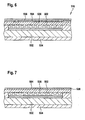
- FIG. 6 1 shows an embodiment of a chip card 516, in which the optical layer 504 is embodied as a lenticular lens, spherical or hexagonal lens grid, line grid or as a holographic or optical microstructure, which is arranged between the cover layer 538 and the separation layer 536.
- the optical layer 504 may also be on the cover layer 538 or form an integral part of the cover layer 538, as shown in FIG FIG. 7 is shown.
- the optical layers of the embodiments considered here can be rigid, dynamic or switchable.
- a dynamic or switchable optical layer can be realized by a further display element or by switchable optical elements that can change their shape, for example due to a control pulse.
- Such a change in shape may be due, for example, to a shape memory effect or due to a piezoelectric effect.
- the triggering of the shape memory effect can be induced by a change in temperature, by radiation, or by an electric or magnetic field.
- FIG. 8 FIG. 12 shows a smart card 616 having an optical layer 604 located between a capping layer 638 and a display layer 602.
- the optical layer 604 has a plurality of lenses 640 arranged in a grid or matrix.
- the lenses 640 are switchable, that is, the shape of the lenses can be changed by a corresponding control signal so that the three-dimensional effect of the image display is switched on or off.
- the FIG. 8 shows the lenses 640 in a preferably unswitched, relaxed state in which the lenses 640 have only a small radius of curvature. Due to a control signal, the lenses 640 transition to a deformed state, which in the FIG. 9 is shown. In the deformed state, the lenses have a greater curvature than in the relaxed state, so that the autostereoscopic three-dimensional effect sets.
- the lens system may also be designed so that a three-dimensional representation takes place in the unswitched, relaxed state.
- a three-dimensional representation can also be made in both states, but the representation is visible at different distances from the display. In this way, for example, can be switched between the observation by a viewer / controller on a multi-user operation.
- the lenses 640 may be made of, for example, a shape memory alloy, the shape memory effect being triggered by the control signal.
- the control signal for example, a circuit is closed, which leads to the heating of the lenses 640, so that they go into a high-temperature form, as in FIG. 9 shown.
- the triggering of the shape memory effect can also be triggered by an external radiation source or by applying an electric or magnetic field.
- the lenses 640 are made of a polymer having piezoelectric properties. By applying an electrical voltage to the lenses 640 deform this then due to the piezoelectric effect in the in the FIG. 9 shown shape.
- the lenses 640 themselves are not directly controllable, for example due to a shape memory or piezoelectric effect, but that one or more actuators are arranged in the chip card 616, which can be controlled by a control signal in order to For example, exert a force on the lenses 640 so that they are reversibly, plastically deformed, as in FIG. 9 shown.
- the FIG. 10 1 shows a chip card 716 in which a further display 704 is arranged between the cover layer 738 and the separation layer 736 covering the display layer 702.
- the display layer 704 serves to reproduce an optical structure, such as a line screen, which effects the autostereoscopic three-dimensional effect.
- the display 704 is an electrochromic system having a transparent electrode structure.
- the FIG. 10 shows the display 704 in the off state, in which the lines 742 are not or almost invisible.
- FIG. 11 shows the display 704 in the on state. When turned on, lines 742 are displayed, resulting in the autostereoscopic three-dimensional effect.
- the display 704 may be, for example, an OLED display, a rotary element display, a bistable electrophoretic display, an electrochromic display, or the like.
- the display layer 702 uses the same or similar technology as used for the display 704.
- the display layer 702 is a printed electrochromic display
- the display 704 is also configured as a printed electrochromic display.
- the display layer is flexible with its optical layer and is, for example, of a film-like design. This opens a wide variety of applications, such as the integration of such a sheet-like display device in a value or security document, a smart card, in a portable electronic device or even use as e-paper.
- the FIG. 12 12 shows a block diagram of a document 844.
- the document 844 may be, for example, a value or security document, such as an identification card, passport, identity card, driver's license, credit card, ID card, or ticket.
- the document 844 may consist essentially of paper and / or plastic or different paper and / or plastic layers.
- the document 844 can also be designed as a so-called chip card, which in turn can be contact-based, contactless or designed as a dual-interface card.
- the document 844 has an integrated electronic circuit 846 that includes a nonvolatile electronic memory 806.
- the memory 806 serves to store image data, in particular stereo image data. Further, the memory 806 may be used to store personal and / or object related data of the document 844 bearer. To protect the data in the
- Memory 806 against unauthorized access is implemented by the integrated electronic circuit 846, a cryptographic protocol 848.
- Document 844 incorporates an embodiment of a display device according to the invention which includes a display layer 802 and a switchable optical layer 804.
- the display layer 802 and the optical layer 804 are driven by the driver 808 of the integrated electronic circuit 846.
- the electronic circuit 846 may consist of a chip or chip module, of two or more chips or chip modules, a combination of chip or chip module and printed electronics or entirely of printed electronics.
- the optical layer 804 includes, for example, switchable optical elements having, for example, a shape memory effect or piezoelectric effect, which can be triggered due to a control pulse emitted by the driver 808, so that the optical elements can change their shape, or another display, for example for displaying barrier lines.
- the integrated electronic circuit 846 is connected to an antenna 850 in a non-contact embodiment, for example.
- the integrated electronic circuit 846 with the antenna 850 are preferably formed in an RFID technology. Other embodiments may be contact-based or dual-interface.
- document 844 does not have its own power supply for the integrated electronic circuit 846 or the display device, but draws power for the operation of the integrated electronic circuit 846 or the display device, for example through the antenna 850 received radio signals.
- the integrated electronic circuit 846 with the antenna 850 is thus, for example, a so-called RFID transponder.
- contact-based and / or contactless interfaces may also be used to power the integrated electronic circuit 846 and / or the display device.
- the power supply is performed by a reading device 852.
- the reader 852 has an RFID interface 854 or other contact-based and / or contactless interface.
- the RFID interface 854 is designed to transmit RFID radio signals and to receive corresponding response signals from the antenna 850.
- the reader 852 has a processor 856 for executing program instructions which control the operation of the reader 852 and a user interface 858, in particular a graphical user interface.
- the processor 856 is for participation in the cryptographic protocol 848, for example, to access the data stored in the memory 806 and / or to trigger a control pulse of the driver 808 to turn the autostereoscopic 3D effect on and off.
- the document 844 may carry an additional imprint 860.
- the imprint 860 is a two-dimensional representation of the three-dimensional object reproduced when the display device is switched on.
- the imprint 860 is the reproduction of a passport photograph. This has the advantage that the document 844 can also be used without the reader 852. If the reader 852 is available, the imprint 860 provides another security feature since the imprint 860 can be visually checked for compliance with the display of the display device 802, 804.
- the FIG. 13 shows a portable electronic device 962.
- the device 962 has a housing which consists of two housing parts 964 and 966.
- the FIG. 13 shows the device 962 with the housing closed.
- a drum 968 is arranged, on which a display layer 902 according to the invention with an optical layer thereon, which correspond, for example, to one of the embodiments described above, is wound up.
- the other end of the display layer 902 or the optical layer is connected to a housing wall 970 of the housing part 966.
- the housing can be opened by pulling the housing parts 964 and 966 apart, as shown in the FIG. 14 is shown.
- a user takes, for example, the housing part 964 in his left hand and the housing part 966 in his right hand and then pulls apart the two housing parts, wherein the display layer 902 unwinds with its optical layer thereon of the drum 968. This creates a relatively large display area 972 between the exploded housing parts 964 and 966.
Abstract
Description
Die Erfindung betrifft ein Dokument mit einer Anzeigevorrichtung zur autostereoskopischen Erzeugung eines dreidimensionalen Bildes sowie elektronisches Papier, insbesondere Wert- und Sicherheitsdokumente, Chipkarten und tragbare elektronische Geräte mit einer solchen Anzeigevorrichtung.The invention relates to a document with a display device for autostereoscopic production of a three-dimensional image and electronic paper, in particular value and security documents, smart cards and portable electronic devices with such a display device.
Aus dem Stand der Technik sind autostereoskopische Verfahren für die Wiedergabe von dreidimensionalen Bildern seit langem bekannt. Im Unterschied zu stereoskopischen Verfahren erfolgt bei autostereoskopischen Verfahren die Erzeugung des dreidimensionalen Büdeindrucks ohne zusätzliche Hilfsmittel, wie zum Beispiel Shutter-Brillen, Rot-Grün-Brillen, Brillen mit Polarisationsfiltern oder Head-Mounted-Displays.Autostereoscopic methods for the reproduction of three-dimensional images have long been known from the prior art. In contrast to stereoscopic methods, the generation of the three-dimensional image impression takes place in the case of autostereoscopic methods without additional aids, such as for example Shutter glasses, red-green glasses, glasses with polarizing filters or head-mounted displays.
Eine autostereoskopische dreidimensionale Bildwiedergabe kann beispielsweise unter Verwendung von so genannten Barriere-Strukturen erfolgen, die auch als Paralax-Barrieren bezeichnet werden.An autostereoscopic three-dimensional image reproduction can take place, for example, using so-called barrier structures, which are also referred to as paralax barriers.
Ferner sind so genannte Integral-Verfahren aus dem Stand der Technik bekannt, bei denen der dreidimensionale Bildeindruck durch eine Vielzahl von Linsen erzeugt wird, zum Beispiel durch eine matrixförmige Anordnung von sphärischen, insbesondere halbkugelförmigen Linsen.Furthermore, so-called integral methods are known from the prior art, in which the three-dimensional image impression is produced by a plurality of lenses, for example by a matrix-like arrangement of spherical, in particular hemispherical lenses.
Ferner ist die autostereoskopische Erzeugung von dreidimensionalen Bilder auch mit Hilfe von holographischen Elementen bzw. holographischen Mikrostrukturen an sich aus dem Stand der Technik bekannt.Furthermore, the autostereoscopic production of three-dimensional images is also known from the prior art with the aid of holographic elements or holographic microstructures.
Darüber hinaus sind so genannte Lentikularverfahren zur Erzeugung autostereoskopischer dreidimensionaler Bilder aus dem Stand der Technik bekannt. Dabei wird zum Beispiel ein Linienraster aus konvexen zylindrischen Linsen, die auch als "Lentikulars" bezeichnet werden, zur Erzeugung des dreidimensionalen Bildeindrucks verwendet.In addition, so-called lenticular methods for generating autostereoscopic three-dimensional images from the prior art are known. In this case, for example, a line grid of convex cylindrical lenses, which are also referred to as "lenticulars", used to generate the three-dimensional image impression.
Einen Überblick über verschiedene vorbekannte autostereoskopische Verfahren gibt insbesondere "History of Lentikular and Related Autostereoscopic Methods", David E. Robersts (http://www.microlens.com/HistoryofLentikular.pdf) sowie "Autostereoskopische Displays", Seminar aktuelle Themen der virtuellen Realität, RWTH Aachen (http://www.rz.rwth-Aachen.de/vr/teaching/seminars/ws2003/Presentation/Eggerath.pdf). An overview of various previously known autostereoscopic procedures are in particular "History of Lenticular and Related Autostereoscopic Methods", David E. Robersts (http://www.microlens.com/HistoryofLentikular.pdf) and "Autostereoscopic Displays", seminar current topics of virtual reality , RWTH Aachen (http://www.rz.rwth-Aachen.de/vr/teaching/seminars/ws2003/Presentation/Eggerath.pdf).
Solche autostereoskopischen Verfahren werden im Stand der Technik für Computer-Monitore eingesetzt. Entsprechende Computer-Monitore sind bekannt aus http://www.research.philips.com/technologies/display/3d/technical.html sowie "
Aus der
Der Erfindung liegt dem gegenüber die Aufgabe zu Grunde, ein verbessertes Dokument mit einer Anzeigevorrichtung zu schaffen.The invention is based on the object to provide an improved document with a display device.
Die der Erfindung zu Grunde liegende Aufgabe wird mit den Merkmalen des Patentanspruchs 1 gelöst. Bevorzugte Ausführungsformen der Erfindung sind in den abhängigen Patentansprüchen angegeben.The object underlying the invention is achieved with the features of claim 1. Preferred embodiments of the invention are indicated in the dependent claims.
Die erfindungsgemäße Anzeigevorrichtung hat eine flexible Anzeigeschicht zur Wiedergabe mindestens eines ersten und eines zweiten Bildes sowie eine flexible optische Schicht, die auf der Anzeigeschicht angeordnet ist und die zur autostereoskopischen Erzeugung eines dreidimensionalen Bildes aus den ersten und zweiten Bildern ausgebildet ist.The display device according to the invention has a flexible display layer for reproducing at least a first and a second image and a flexible optical layer which is arranged on the display layer and which is designed for the autostereoscopic production of a three-dimensional image from the first and second images.
Die ersten und zweiten Bilder zeigen zum Beispiel dasselbe Objekt aus leicht unterschiedlichen Winkeln. Die entsprechenden Bilddaten können als so genannte Stereodaten vorliegen. Es kann sich hierbei um Stereodaten handeln, die durch ein Aufnahmeverfahren von einem realen Objekt aufgenommen wurden oder um synthetische, das heißt durch Computerberechnung erzeugte Stereodaten. Im letzteren Falle können die Stereodaten durch Vorausberechnung oder in Echtzeit gewonnen werden.For example, the first and second images show the same object from slightly different angles. The corresponding image data can be present as so-called stereo data. This can be stereo data recorded by a recording method from a real object or synthetic stereo data, that is, computationally generated stereo data. In the latter case, the stereo data can be obtained by prediction or in real time.
Die vorliegende Erfindung ist besonders vorteilhaft, da sowohl die Anzeigeschicht als auch die darüber angeordnete optische Schicht flexibel sind. Dies ermöglicht eine Ausbildung der Anzeigevorrichtung in flexibler Bauform, wie z.B. in der Form einer flexiblen Folie. Hierfür geeignete Anzeigeschichten sind erfindungsgemäß als LED-Anzeige, insbesondere OLED-Anzeige, als Drehelementanzeige, als elektrochrome Anzeige und/oder als elektrophoretische Anzeige ausgebildet.The present invention is particularly advantageous because both the display layer and the optical layer disposed above are flexible. This allows a design of the display device in flexible design, such. in the form of a flexible film. According to the invention, display layers suitable for this purpose are designed as LED displays, in particular OLED displays, as rotary element displays, as electrochromic displays and / or as electrophoretic displays.
Nach einer Ausführungsform der Erfindung ist die Anzeigeschicht der Anzeigevorrichtung als Light Emitting Diode (LED) Anzeige ausgebildet. Vorzugsweise handelt es sich um eine Organic Light Emitting Diode (OLED) Anzeige, die zum Beispiel auf eine flexible Trägefolie aufgedruckt ist. Eine weitere bevorzugte Ausführungsform ist eine so genannte Hybrid-LED, bei der sowohl anorganische wie organische Materialien verwendet werden.According to one embodiment of the invention, the display layer of the display device is designed as a light emitting diode (LED) display. Preferably, it is an Organic Light Emitting Diode (OLED) display, which is printed on a flexible carrier foil, for example. Another preferred embodiment is a so-called hybrid LED using both inorganic and organic materials.
Beispielsweise kann die Anzeigeschicht als OLED-Display-Folie ausgebildet sein. Die Herstellung solcher OLED-Display-Folien ist an sich aus dem Stand der Technik bekannt und basiert beispielsweise auf der Low Temperature Polysilicon (LTPS)-Technik (vgl. hierzu http://www.sharpsma.com/Icd/Icdguide/Technologies/OLED_displays.php). Es können aber auch andere polymerelektronische Verfahren zum Aufbringen, wie zum Beispiel zum Aufdrucken, der Anzeige auf einem flexiblen Träger eingesetzt werden.For example, the display layer may be formed as an OLED display film. The production of such OLED display films is known per se from the prior art and is based, for example, on the low-temperature polysilicon (LTPS) technique (for this see http://www.sharpsma.com/Icd/Icdguide/Technologies/). OLED_displays.php). However, other polymeric electronic methods of application such as printing on a flexible support may also be used.
Nach einer Ausführungsform der Erfindung ist die Anzeigeschicht als so genannte Drehelement-Anzeige ausgebildet. Drehelement-Anzeigen sind an sich aus dem Stand der Technik bekannt und beinhalten drehbare Elemente, wie etwa Zylinder, Polyeder oder Kugeln. Diese drehbaren Elemente sind typischerweise in einem Substrat eingebettet und ein geringer Zwischenraum zwischen jedem drehbaren Element und dem Substrat ist mit einer Flüssigkeit gefüllt, so dass sich die Elemente in einem sich verändernden elektrischen Feld frei drehen, aber nicht von einem Ort zum andern wandern können.According to one embodiment of the invention, the display layer is designed as a so-called rotary element display. Rotary element indicators are well known in the art and include rotatable elements such as cylinders, polyhedrons, or balls. These rotatable elements are typically embedded in a substrate and a small gap between each rotatable element and the substrate is filled with a liquid so that the elements are free to rotate in a changing electric field but can not migrate from one place to another.
Wenn zum Beispiel eine Halbkugel eines drehbaren Elements schwarz ist und die andere weiß ist, kann jeder Bildpunkt durch das an dieser Stelle angelegte elektrische Feld an- und ausgeschaltet werden. Mit Hilfe einer Drehelement-Anzeige lässt sich insbesondere so genanntes elektronisches Papier, das auch als E-Paper bezeichnet wird, realisieren.For example, if one hemisphere of a rotatable element is black and the other is white, each pixel may be turned on and off by the electric field applied at that location. With the aid of a rotary element display, in particular so-called electronic paper, which is also referred to as e-paper, can be realized.
Ausführungsformen von Drehelement-Anzeigen, die auf der Drehung von Teilchen aufgrund eines elektrischen Feldes basieren, sind unter anderem bekannt aus
Ferner ist aus der
Nach einer Ausführungsform der Erfindung ist die Anzeigeschicht als elektrochromes oder elektrophoretisches Display ausgebildet.According to one embodiment of the invention, the display layer is designed as an electrochromic or electrophoretic display.
Nach einer Ausführungsform der Erfindung ist die Anzeigeschicht als Aktiv-Matrix oder als Passiv-Matrix ausgebildet. Anstelle einer Matrix von getrennt ansteuerbaren Bildpunkten kann die Anzeigeschicht auch zum Beispiel durch Aufdruck eines lichtemittierenden Polymers erzeugt werden, welches nur insgesamt zur Wiedergabe eines fest vorgegebenen Bildes ansteuerbar ist.According to one embodiment of the invention, the display layer is formed as an active matrix or as a passive matrix. Instead of a matrix of separately controllable pixels, the display layer can also be produced, for example, by imprinting a light-emitting polymer which can only be controlled to reproduce a fixed image.
Eine weitere Ausführungsform verwendet eine vollflächige Kontaktierung der Elektroden des Displays ohne die Ausführung als Matrix. Da auf diese Weise keine gezielte Ansteuerung der Bildpunkte möglich ist, werden die Bildinformation entweder aufbauend, zum, Beispiel drucktechnisch, oder destruktiv, zum Beispiel mittels Laser-Personalisierung, eingebracht. Dieses hat den Vorteil, dass eine spätere Manipulation der eingebrachten Daten faktisch nicht mehr möglich ist. Des weiteren benötigt ein solcher Aufbau keinen zusätzlich Treiber für die Aktiv-Matrix, was die Integration in ein Dokument erleichtert.Another embodiment uses a full-area contacting of the electrodes of the display without the implementation as a matrix. Since no targeted control of the pixels is possible in this way, the image information either constructive, for example, printing technology, or destructive, for example by means of Laser personalization, introduced. This has the advantage that later manipulation of the introduced data is in fact no longer possible. Furthermore, such a structure does not require additional drivers for the active matrix, which facilitates integration into a document.
Nach einer Ausführungsform der Erfindung weist die optische Schicht eine Barriere-Struktur auf. Hierbei kann es sich zum Beispiel um eine Barriere-Maske oder ein Barriere-Gitter handeln, welches starr oder dynamisch ausgebildet sein kann.According to one embodiment of the invention, the optical layer has a barrier structure. This may be, for example, a barrier mask or a barrier grid, which may be rigid or dynamic.
Nach einer Ausführungsform der Erfindung hat die optische Schicht eine Vielzahl von optischen Linsen, insbesondere eine Matrix sphärischer Linsen oder halbkugelförmiger Linsen zur Realisierung eines so genannten Integral-Verfahrens.According to one embodiment of the invention, the optical layer has a multiplicity of optical lenses, in particular a matrix of spherical lenses or hemispherical lenses, for implementing a so-called integral method.
Nach einer Ausführungsform der Erfindung hat die optische Schicht holographische oder optische Mikrostrukturen zur autostereoskopischen Erzeugung des dreidimensionalen Bildeindrucks.According to one embodiment of the invention, the optical layer has holographic or optical microstructures for autostereoscopic production of the three-dimensional image impression.
Nach einer Ausführungsform der Erfindung hat die optische Schicht eine lentikulare Struktur, wie zum Beispiel linienförmig nebeneinander angeordnete plano-konvexe zylindrische Linsen, das heißt so genannten "Lentikulars".According to one embodiment of the invention, the optical layer has a lenticular structure, such as linearly juxtaposed plano-convex cylindrical lenses, that is, so-called "lenticulars".
Nach einer Ausführungsform der Erfindung ist die Anzeigevorrichtung zur Erzeugung einer Vielzahl von autostereoskopischen Bildern zur Betrachtung eines abgebildeten Objekts aus verschiedenen Blickwinkeln ausgebildet.According to one embodiment of the invention, the display device is designed to generate a plurality of autostereoscopic images for viewing an imaged object from different angles.
Nach einer Ausführungsform der Erfindung ist die optische Schicht schaltbar ausgebildet, um zum Beispiel den autostereoskopischen 3D-Effekt der Bildwiedergabe ein- oder ausschalten zu können.According to one embodiment of the invention, the optical layer is designed to be switchable, for example to enable or disable the autostereoscopic 3D effect of image reproduction.
Nach einer Ausführungsform der Erfindung weist die optische Schicht zumindest ein Formgedächtniselement aus einer so genannten Formgedächtnislegierung auf. Durch Auslösung des Formgedächtniseffekts erfährt die optische Schicht eine Formänderung aufgrund derer die autostereoskopische Bildwiedergabe ein- bzw. ausgeschaltet wird.According to one embodiment of the invention, the optical layer has at least one shape memory element made of a so-called shape memory alloy. By triggering the shape memory effect, the optical layer undergoes a change in shape on the basis of which the autostereoscopic image reproduction is switched on or off.
Beispielsweise hat die optische Schicht optische Elemente, wie zum Beispiel Linsen, deren Linsenradius durch Auslösung des Formgedächtniseffekts variiert wird. Die Linsen können dabei selbst aus einer Formgedächtnislegierung bestehen oder durch ein oder mehrere separate Formgedächtniselemente der optischen Schicht elastisch verformt werden.For example, the optical layer has optical elements, such as lenses, whose lens radius is varied by triggering the shape memory effect. The lenses may themselves consist of a shape memory alloy or be elastically deformed by one or more separate shape memory elements of the optical layer.
Dabei kann es sich um eine Formgedächtnislegierung handeln, deren Formänderung Temperatur, Strahlungs- oder durch ein elektrisches oder magnetisches Feld induzierbar ist.It may be a shape memory alloy whose shape change temperature, radiation or by an electric or magnetic field is inducible.
Nach einer Ausführungsform der Erfindung beinhaltet die optische Schicht ein piezo-elektrisches Element. Durch Ansteuerung des piezo-elektrischen Elements erfährt die optische Schicht eine Formänderung, um zum Beispiel den 3D-Effekt ein- bzw. auszuschalten. Beispielsweise weist die optische Schicht optische Elemente, wie zum Beispiel Linsen auf, die aus einem piezo-elektrischen Material, vorzugsweise einem piezoelektrischen Polymer bestehen. Durch Auslösung des piezoelektrischen Effekts mit Hilfe eines entsprechenden Steuersignals verändern die optischen Elemente, das heißt beispielsweise die Linsen, ihre Form so, dass der 3D-Effekt ein- oder ausgeschaltet wird.According to one embodiment of the invention, the optical layer includes a piezoelectric element. By driving the piezoelectric element, the optical layer undergoes a change in shape, for example to switch the 3D effect on or off. For example, the optical layer has optical elements, such as lenses, which consist of a piezoelectric material, preferably a piezoelectric polymer. By triggering the piezoelectric effect with the aid of a corresponding control signal, the optical elements, that is to say, for example, the lenses, change their shape in such a way that the 3D effect is switched on or off.
Nach einer Ausführungsform der Erfindung ist die optische Schicht selbst als weitere Anzeigeschicht ausgebildet. Zur Realisierung der weiteren Anzeigeschicht können dieselben oder ähnliche Technologien, die zur Realisierung der Anzeigeschicht für die Bildwiedergabe verwendet werden. Insbesondere kann die optische Schicht als elektrochrome oder flüssigkristalline Anzeige ausgebildet sein, Ein Drehelementanzeigeelement kann verwendet werden, wenn dieses zwischen einem transparenten und einem absorbierenden Zustand geschaltet werden kann. Beispielsweise werden auf der Anzeigschicht, durch welche die optische Schicht gebildet wird, Barriere-Linien oder ein Barriere-Gitter angezeigt.According to one embodiment of the invention, the optical layer itself is formed as a further display layer. To realize the further display layer, the same or similar technologies used to realize the display layer for image reproduction may be used. In particular, the optical layer may be formed as an electrochromic or liquid crystal display. A rotary element display element may be used if it can be switched between a transparent and an absorbing state. For example, barrier lines or a barrier grid are displayed on the display layer through which the optical layer is formed.
Nach einer Ausführungsform der Erfindung hat die Anzeigevorrichtung einen elektronischen Speicher zur Speicherung von Bilddaten für die Wiedergabe der zumindest ersten und zweiten Bilder auf der flexiblen Anzeigeschicht. Bei den Bilddaten handelt es sich um ein oder mehrere Stereobilddatensätze.According to one embodiment of the invention, the display device has an electronic memory for storing image data for the reproduction of at least first and second images on the flexible display layer. The image data is one or more stereo image data sets.
Nach einer Ausführungsform der Erfindung hat die Anzeigevorrichtung einen integrierten elektronischen Schaltkreis zur Durchführung eines kryptographischen Protokolls, um den elektronischen Speicher vor unerlaubten Zugriffen zu schützen.According to one embodiment of the invention, the display device has an integrated electronic circuit for performing a cryptographic protocol to protect the electronic memory from unauthorized access.
Nach einer Ausführungsform der Erfindung hat die Anzeigevorrichtung eine Energiequelle, wie zum Beispiel eine Batterie, eine Solarzelle oder ein thermoelektrisches Element, wie z.B. eine Seebeck- oder Peltier-Element.According to one embodiment of the invention, the display device has a power source, such as a battery, a solar cell or a thermoelectric element, such as e.g. a sea bass or peltier element.
Nach einer Ausführungsform der Erfindung ist die Anzeigevorrichtung für eine externe Energieversorgung ausgebildet, wie zum Beispiel über eine kontaktbehaftete und / oder
eine kontaktlose Schnittstelle. Beispielsweise kann die Schnittstelle eine Antenne aufweisen, wobei die Energieversorgung durch über die Antenne empfangene Funksignale erfolgt. Alternativ oder zusätzlich kann die Anzeigevorrichtung eine Induktionsspule aufweisen, um induktiv mit Energie versorgt zu werden.According to one embodiment of the invention, the display device is designed for an external power supply, such as via a contact-related and / or
a contactless interface. For example, the interface may comprise an antenna, wherein the power supply is effected by radio signals received via the antenna. Alternatively or additionally, the display device may comprise an induction coil for being supplied with energy inductively.
Nach einer Ausführungsform der Erfindung ist die Anzeigevorrichtung als RFID Transponder ausgebildet oder mit einem solchen verbunden. In diesem Fall kann der RFID Transponder als Energiequelle für die Anzeigevorrichtung dienen.According to one embodiment of the invention, the display device is designed as an RFID transponder or connected to such. In this case, the RFID transponder can serve as an energy source for the display device.
Nach einer Ausführungsform der Erfindung trägt die Anzeigevorrichtung eine zusätzliche zweidimensionale Darstellung des dreidimensionalen Bildes. Diese zweidimensionale Darstellung kann zum Beispiel auf der Anzeigevorrichtung aufgedruckt sein oder mit Hilfe einer weiteren separaten Anzeige, die ohne Energieversorgung auskommt, dargestellt werden. Dies hat den Vorteil, dass auch dann eine Darstellung des Bildes erfolgt, wenn keine Energieversorgung zur Verfügung steht. Durch die Vergleichsmöglichkeit der zweidimensionalen Darstellung mit der dreidimensionalen Bilddarstellung ist ferner ein weiteres Sicherheitsmerkmal gegeben. Nach einer Ausführungsform der Erfindung dient eine erfindungsgemäße Anzeigevorrichtung zur Realisierung eines Dokuments. Dabei kann das Dokument durch die Anzeigevorrichtung selbst gebildet werden oder die Anzeigevorrichtung kann in ein Dokument integriert sein. Bei dem Dokument kann es sich zum Beispiel um ein Wert-, Sicherheits- oder Identifikationsdokument handeln, wie zum Beispiel eine Identifikationskarte, Reisepass, Personalausweis, Führerschein, Kreditkarte, Kundenausweis oder Fahrausweis. Insbesondere kann das Dokument als Chipkarte ausgebildet sein.According to one embodiment of the invention, the display device carries an additional two-dimensional representation of the three-dimensional image. This two-dimensional representation can, for example, be printed on the display device or can be represented by means of a further separate display, which manages without a power supply. This has the advantage that even then a representation of the image takes place when no power supply is available. Due to the possibility of comparing the two-dimensional representation with the three-dimensional image representation, a further security feature is also provided. According to one embodiment of the invention, a display device according to the invention is used for the realization of a document. In this case, the document can be formed by the display device itself or the display device can be integrated into a document. The document may be, for example, a value, security or identification document, such as an identification card, passport, identity card, driver's license, credit card, ID card or ticket. In particular, the document can be designed as a chip card.
Nach einer Ausführungsform der Erfindung ist die erfindungsgemäße Anzeigevorrichtung in ein tragbares elektronisches Gerät integriert, wie zum Beispiel in ein so genanntes elektronisches Buch (E-Book), ein mobiles Telekommunikationsgerät, wie zum Beispiel ein Mobiltelefon, Smart Phone oder dergleichen, einen tragbaren Computer oder einen Personal Digital Assistant (PDA).According to one embodiment of the invention, the display device according to the invention is integrated in a portable electronic device, such as in a so-called electronic book (e-book), a mobile telecommunication device, such as a mobile phone, smart phone or the like, a portable computer or a Personal Digital Assistant (PDA).
Vorzugsweise hat das elektronische Gerät einen Stauraum, wobei die Anzeigevorrichtung in eine Stauposition innerhalb des Stauraums einrollbar ist. Dadurch
kann ein tragbares elektronisches Gerät geschaffen werden, welches die autostereoskopische Bildwiedergabe bei gleichzeitig besonders kompakter Bauweise ermöglicht.Preferably, the electronic device has a storage space, wherein the display device can be rolled into a stowed position within the storage space. Thereby
a portable electronic device can be created, which allows the autostereoscopic image reproduction at the same time very compact design.
Nach einer Ausführungsform der Erfindung hat das Dokument eine Anzeigevorrichtung, wobei die Anzeigevorrichtung folgendes beinhaltet: eine flexiblen Anzeigeschicht zur Wiedergabe zumindest eines ersten und/oder eines zweiten Bildes, eine flexible optische Schicht, die auf der Anzeigeschicht angeordnet ist, wobei die optische Schicht zur autostereoskopischen Erzeugung eines dreidimensionalen Bildes aus den ersten und zweiten Bildern ausgebildet ist, wobei die Anzeigeschicht als LED-Anzeige, insbesondere als OLED-Anzeige, als Drehelementanzeige, als elektrochrome Anzeige und/oder als elektrophoretische Anzeige ausgebildet ist.According to one embodiment of the invention, the document has a display device, the display device comprising: a flexible display layer for displaying at least a first and / or a second image, a flexible optical layer disposed on the display layer, the optical layer being autostereoscopic Forming a three-dimensional image from the first and second images is formed, wherein the display layer as an LED display, in particular as an OLED display, as a rotary element display, as an electrochromic display and / or as an electrophoretic display is formed.
Nach einer Ausführungsform der Erfindung ist die optische Schicht schaltbar, um die autostereoskopische Erzeugung des dreidimensionalen Bildes ein- oder auszuschalten.According to one embodiment of the invention, the optical layer is switchable to turn on or off the autostereoscopic production of the three-dimensional image.
Nach einer Ausführungsform der Erfindung hat die Anzeigeschicht einen flexiblen Träger, auf den ein leitfähiges Polymer aufgedruckt ist.According to one embodiment of the invention, the display layer has a flexible support on which a conductive polymer is printed.
Nach einer Ausführungsform der Erfindung ist die Anzeige bistabil.According to one embodiment of the invention, the display is bistable.
Nach einer Ausführungsform der Erfindung ist die Anzeigeschicht als Aktiv-Matrixanzeige ausgebildet.According to one embodiment of the invention, the display layer is formed as an active matrix display.
Nach einer Ausführungsform der Erfindung ist die Anzeigeschicht als Passiv-Matrixanzeige ausgebildet.According to one embodiment of the invention, the display layer is designed as a passive matrix display.
Nach einer Ausführungsform der Erfindung ist die Anzeigeschicht ohne Matrix ausgebildet ist und nur an entsprechenden Bildpunkten sind die kontrastgebenden Elemente aufgedruckt.According to one embodiment of the invention, the display layer is formed without matrix and only at corresponding pixels, the contrasting elements are printed.
Nach einer Ausführungsform der Erfindung ist die Anzeigeschicht vollflächig und ohne Matrix ausgebildet, so dass einzelne Bildpunkte für eine Personalisierung deaktivierbar sind.According to one embodiment of the invention, the display layer is formed over the entire area and without a matrix, so that individual pixels can be deactivated for personalization.
Nach einer Ausführungsform der Erfindung ist die Anzeigeschicht so ausgebildet, dass die Deaktivierung mittels eines Lasers erfolgen kann.According to one embodiment of the invention, the display layer is designed so that the deactivation can take place by means of a laser.
Nach einer Ausführungsform der Erfindung beinhaltet die Anzeigeschicht aufgedruckte Bildelemente.According to one embodiment of the invention, the display layer includes printed pixels.
Nach einer Ausführungsform der Erfindung weist die optische Schicht eine Barriere-Struktur auf.According to one embodiment of the invention, the optical layer has a barrier structure.
Nach einer Ausführungsform der Erfindung weist die optische Schicht ein Linienraster auf.According to one embodiment of the invention, the optical layer has a line grid.
Nach einer Ausführungsform der Erfindung weist die optische Schicht eine Vielzahl von optischen Linsen auf.According to one embodiment of the invention, the optical layer comprises a plurality of optical lenses.
Nach einer Ausführungsform der Erfindung weist die optische Schicht eine Beugungsstruktur auf.According to one embodiment of the invention, the optical layer has a diffraction structure.
Nach einer Ausführungsform der Erfindung weist die optische Schicht eine holographische oder optische Mikrostruktur auf.According to one embodiment of the invention, the optical layer has a holographic or optical microstructure.
Nach einer Ausführungsform der Erfindung weist die optische Schicht eine lentikulare Struktur auf.According to one embodiment of the invention, the optical layer has a lenticular structure.
Nach einer Ausführungsform der Erfindung ist die optische Schicht zur autostereoskopischen Erzeugung mehrerer dreidimensionaler Bilder aus entsprechenden mehreren ersten und zweiten Bildern zur Betrachtung eines abgebildeten Objekts aus verschiedenen Winkeln ausgebildet.According to one embodiment of the invention, the optical layer is designed for autostereoscopic production of a plurality of three-dimensional images from corresponding multiple first and second images for viewing an imaged object from different angles.
Nach einer Ausführungsform der Erfindung weist die optische Schicht ein Formgedächtniselement auf, wobei durch Auslösung des Formgedächtniseffekts die autostereoskopische Erzeugung des dreidimensionalen Bildes ein- oder ausschaltbar ist.According to one embodiment of the invention, the optical layer has a shape memory element, wherein the autostereoscopic generation of the three-dimensional image can be switched on or off by triggering the shape memory effect.
Nach einer Ausführungsform der Erfindung weist die optische Schicht ein piezoelektrisches Element auf, durch dessen Aktivierung die optische Schicht eine Formänderung erfährt, wodurch die autostereoskopische Erzeugung des dreidimensionalen Bildes ein- oder ausschaltbar ist.According to one embodiment of the invention, the optical layer has a piezoelectric element, by the activation of which the optical layer undergoes a change in shape, whereby the autostereoscopic generation of the three-dimensional image can be switched on or off.
Nach einer Ausführungsform der Erfindung beinhaltet die optische Schicht piezoelektrisch ansteuerbare Polymerlinsen.According to one embodiment of the invention, the optical layer includes piezoelectrically controllable polymer lenses.
Nach einer Ausführungsform der Erfindung ist die optische Schicht durch eine zweite Anzeigeschicht realisiert.According to one embodiment of the invention, the optical layer is realized by a second display layer.
Nach einer Ausführungsform der Erfindung weist die optische Schicht eine flüssigkristalline Anzeige auf.According to one embodiment of the invention, the optical layer has a liquid-crystalline display.
Nach einer Ausführungsform der Erfindung hat das Dokument einen elektronischen Speicher für Bilddaten der zumindest ersten und/oder zweiten Bilder.According to one embodiment of the invention, the document has an electronic memory for image data of the at least first and / or second images.
Nach einer Ausführungsform der Erfindung ist die Anzeigeschicht zur Widergabe des ersten Bildes ausgebildet und das zweite Bild aufgedruckt.According to one embodiment of the invention, the display layer is designed for the reproduction of the first image and the second image is printed.
Nach einer Ausführungsform der Erfindung sind die Bilddaten des ersten Bildes ohne die Bilddaten des zweiten Bildes in dem elektronischen Speicher gespeichert.According to one embodiment of the invention, the image data of the first image without the image data of the second image are stored in the electronic memory.
Nach einer Ausführungsform der Erfindung hat das Dokument einen integrierten elektronischen Schaltkreis zur Durchführung eines kryptographischen Verfahrens als Zugriffsschutz für den elektronischen Speicher.According to one embodiment of the invention, the document has an integrated electronic circuit for performing a cryptographic method as access protection for the electronic memory.
Nach einer Ausführungsform der Erfindung hat das Dokument eine Energiequelle.According to one embodiment of the invention, the document has a power source.
Nach einer Ausführungsform der Erfindung hat das Dokument eine kontaktbehaftete und / oder kontaktlose Schnittstelle zur Energieversorgung.According to one embodiment of the invention, the document has a contact-type and / or contactless interface to the power supply.
Nach einer Ausführungsform der Erfindung hat das Dokument einen RFID Transponder zur Ansteuerung der Anzeigeschicht und / oder der optischen Schicht.According to one embodiment of the invention, the document has an RFID transponder for controlling the display layer and / or the optical layer.
Nach einer Ausführungsform der Erfindung dient der RFID Transponder zur Energieversorgung der Anzeigeschicht und / oder der optischen Schicht.According to one embodiment of the invention, the RFID transponder is used to supply power to the display layer and / or the optical layer.
Nach einer Ausführungsform der Erfindung hat das Dokument eine zusätzliche zweidimensionalen Darstellung des autostereoskopischen Bildes.According to one embodiment of the invention, the document has an additional two-dimensional representation of the autostereoscopic image.
Nach einer Ausführungsform der Erfindung ist die zusätzliche Darstellung aufgedruckt.According to one embodiment of the invention, the additional representation is printed.
Nach einer Ausführungsform der Erfindung ist die Anzeigevorrichtung als elektronisches Papier ausgebildet.According to one embodiment of the invention, the display device is designed as electronic paper.
Nach einer Ausführungsform der Erfindung handelt es sich bei dem Dokument um ein Wert- oder Sicherheitsdokument, insbesondere eine Identifikationskarte, Reisepass, Personalausweis, Führerschein, Kreditkarte, Kundenausweis oder Fahrausweis, oder um eine Chipkarte.According to one embodiment of the invention, the document is a value or security document, in particular an identification card, passport, identity card, driving license, credit card, customer card or ticket, or a chip card.
In einen weiteren Aspekt betrifft die Erfindung ein elektronisches Gerät mit einer Anzeigevorrichtung, wobei die Anzeigevorrichtungfolgendes beinhaltet: eine flexiblen Anzeigeschicht zur Wiedergabe zumindest eines ersten und/oder eines zweiten Bildes, eine optischen Schicht, die auf der Anzeigeschicht angeordnet ist, wobei die optische Schicht zur autostereoskopischen Erzeugung eines dreidimensionalen Bildes aus den ersten und zweiten Bildern ausgebildet ist, wobei die Anzeigeschicht als LED-Anzeige, insbesondere als OLED-Anzeige, als Drehelementanzeige, als elektrochrome Anzeige und/oder als elektrophoretische Anzeige ausgebildet ist.In a further aspect, the invention relates to an electronic device with a display device, the display device comprising: a flexible display layer for displaying at least a first and / or a second image, an optical layer disposed on the display layer, the optical layer being connected to the Autostereoscopic generation of a three-dimensional image from the first and second images is formed, wherein the display layer is designed as an LED display, in particular as an OLED display, as a rotary element display, as an electrochromic display and / or as an electrophoretic display.
Nach einer Ausführungsform der Erfindung ist die Anzeigevorrichtung in eine Stauposition einrollbar.According to one embodiment of the invention, the display device can be rolled into a stowed position.
Nach einer Ausführungsform der Erfindung handelt es sich bei dem elektronischen Gerät um ein elektronisches Buch, ein mobiles Telekommunikationsgerät, einen tragbaren Computer oder einen Personal Digital Assistant (PDA).According to one embodiment of the invention, the electronic device is an electronic book, a mobile telecommunication device, a portable computer or a personal digital assistant (PDA).
Nach einer Ausführungsform der Erfindung handelt es sich bei dem elektronischen Gerät um ein tragbares Gerät.According to one embodiment of the invention, the electronic device is a portable device.
Im weiteren werden bevorzugte Ausführungsformen der Erfindung mit Bezugnahme auf die Zeichnungen näher erläutert. Es zeigen:
- Figur 1
- ein Blockdiagramm einer Ausführungsform einer erfindungsgemäßen Anzeigevorrichtung,
- Figur 2
- eine Chipkarte mit einer Ausführungsform einer erfindungsgemäßen Anzeigevorrichtung bei ausgeschaltetem 3D-Effekt,
- Figur 3
- die Chipkarte der
Figur 2 bei eingeschaltetem 3D-Effekt, - Figur 4
- eine Ausführungsform einer erfindungsgemäßen Anzeigevorrichtung mit Lentikulars,
- Figur 5
- eine Ausführungsform einer erfindungsgemäßen Anzeigevorrichtung mit einem Linienraster,
- Figur 6
- einer Ausführungsform einer erfindungsgemäßen Vorrichtung mit einer optisch aktiven Folie,
- Figur 7
- eine Ausführungsform einer erfindungsgemäßen Vorrichtung mit einer holographischen Folie,
- Figur 8
- eine Ausführungsform einer erfindungsgemäßen Vorrichtung mit optischen Elementen in einem ersten Zustand,
- Figur 9
- die Ausführungsform der
Figur 8 , wenn die optischen Elemente in einem zweiten Zustand vorliegen, - Figur 10
- eine Ausführungsform einer erfindungsgemäßen Vorrichtung mit zum Beispiel elektrochromen Materialien zur schaltbaren Erzeugung von Linien- oder optischen Mikrostrukturen im transparenten Zustand,
- Figur 11
- die Ausführungsform der
Figur 10 im nicht transparentem Zustand, - Figur 12
- ein Blockdiagramm einer Ausführungsform eines erfindungsgemäßen Dokuments mit einem Lesegerät,
- Figur 13
- eine Ausführungsform eines erfindungsgemäßen tragbaren elektronischen Geräts in geschlossenem Zustand,
- Figur 14
- das elektronische Gerät der
Figur 13 in geöffnetem Zustand.
- FIG. 1
- a block diagram of an embodiment of a display device according to the invention,
- FIG. 2
- a chip card with an embodiment of a display device according to the invention with the 3D effect switched off,
- FIG. 3
- the chip card of
FIG. 2 when the 3D effect is switched on, - FIG. 4
- an embodiment of a display device according to the invention with lenticulars,
- FIG. 5
- an embodiment of a display device according to the invention with a line grid,
- FIG. 6
- an embodiment of a device according to the invention with an optically active film,
- FIG. 7
- an embodiment of a device according to the invention with a holographic film,
- FIG. 8
- an embodiment of a device according to the invention with optical elements in a first state,
- FIG. 9
- the embodiment of the
FIG. 8 when the optical elements are in a second state, - FIG. 10
- an embodiment of a device according to the invention with, for example, electrochromic materials for the switchable generation of line or optical microstructures in the transparent state,
- FIG. 11
- the embodiment of the
FIG. 10 in a non-transparent state, - FIG. 12
- a block diagram of an embodiment of a document according to the invention with a reader,
- FIG. 13
- an embodiment of a portable electronic device according to the invention in the closed state,
- FIG. 14
- the electronic device of
FIG. 13 in open condition.
In der nachfolgenden Figurenbeschreibung werden einander entsprechende Elemente mit entsprechenden Bezugszeichen gekennzeichnet.In the following description of the figures corresponding elements will be marked with corresponding reference numerals.
Die
Bei der Anzeigeschicht 102 handelt es sich vorzugsweise um eine flexible OLED-Folie, eine als flexible Folie realisierte Drehelementanzeige, ein bistabiles elektrophoretisches Display, ein elektrophoretisches Display oder eine andere Displaytechnologie,The
Die Anzeigeschicht 102 kann als Aktiv- oder Passiv-Matrix mit separat ansteuerbaren Bildelementen ausgebildet sein. Die Anzeigeschicht 102 kann aber auch durch ein auf einem flexiblen Träger aufgebrachtes Display gebildet werden, welches keine einzeln ansteuerbaren Bildpunkte beinhaltet, sondern nur insgesamt ein- oder ausgeschaltet werden kann, um eine fest vorgegebene Bildinformation darzustellen. Bevorzugt handelt es sich hierbei um ein drucktechnisch hergestelltes Display auf OLED-Basis. Dieses kann durch entweder aufbauend durch gezielten Druck nur der benötigtenThe
Bildpunkte oder destruktiv durch gezielte Zerstörung einzelner Bildelemente, zum Beispiel mittels eines Lasers, personalisiert sein.Pixels or destructive by targeted destruction of individual pixels, for example by means of a laser, be personalized.
Ferner ist es auch möglich, dass die Anzeigeschicht 102 ein mittels einer Druckfarbe aufgedrucktes Bild beinhaltet, oder dass ein solches Bild auf der optischen Schicht 104 aufgedruckt ist oder auf einer unterhalb der Anzeigeschicht 102 befindlichen Schicht (in der
Die Anzeigeschicht 102 dient zur Wiedergabe von zumindest ersten und zweiten Bildern, welche die Grundlage für die autostereoskopische Bilderzeugung durch die optische Schicht 104 bilden. Hierzu weist die optische Schicht 104 beispielsweise starre oder dynamische Paralax-Barrieren, Lentikulars, eine Linsenmatrix von sphärischen oder halbkugelförmigen Linsen und / oder andere hologprahische oder optische Mikrostrukturen für die autostereoskopische Erzeugung eines dreidimensionalen Bildes aus den zumindest ersten und zweiten Bildern, die von der Anzeigeschicht wiedergegeben werden, auf.The
Die optische Schicht 104 kann selbst durch eine weitere flexible Anzeigeschicht realisiert werden, wie zum Beispiel durch eine elektrochrome Anzeige, eine Drehelement-Anzeige, ein bistabiles elektrophoretisches Display, ein bistabiles flüssigkristallines Display oder eine andere E-Paper-Technologie, welche über einen transparenten und einen nicht transparenten Zustand verfügt. Durch die die optische Schicht 104 bildende Anzeige werden zum Beispiel Paralax-Barrieren angezeigt. Dabei ist eine Ausbildung der optischen Schicht 104 als bistabile Anzeige besonders vorteilhaft, da dann die gewünschte optische Struktur ohne ständige Energiezufuhr angezeigt werden kann.The
In der hier betrachteten Ausführungsform mit einem Aktiv- oder Passiv-Matrix-Display hat die Anzeigevorrichtung 100 einen Bilddatenspeicher 106, in dem Bilddaten für die Wiedergabe von zumindest einem ersten und zweiten Bild gespeichert sind. Die entsprechenden Bild-Stereodaten können dabei durch ein stereoskopisches Verfahren von einem realen Objekt aufgenommen werden, wie zum Beispiel durch die Aufnahme verschiedener Bilder desselben Objekts aus leicht unterschiedlichen Richtungen. Auf die in dem Bildspeicher 106 gespeicherten Stereodaten greift ein Treiber 108 zu, der die Anzeigeschicht 102 entsprechend zur Wiedergabe der ersten und zweiten Bilder ansteuert. Aufgrund der optischen Schicht 104 nimmt ein Benutzer 110 beispielsweise mit seinem rechten Auge 112 das erste Bild und mit seinem linken Auge 114 das zweite Bild war, so dass der 3D-Effekt resultiert.In the embodiment considered here with an active or passive matrix display, the
Wenn zum Beispiel unterhalb der Anzeigeschicht 102 ein zweidimensionales Bild zum Beispiel auf einen flexiblen Träger aufgedruckt ist, ist es nicht unbedingt erforderlich, dass in dem Bilddatenspeicher Stereobilder gespeichert sind. In diesem Fall wird zum Beispiel durch das fest auf dem Träger aufgedruckte Bild das erste Bild und durch ein zusätzlich von der Anzeigeschicht 102 wiedergegebenes Bild das zweite Bild für die autostereoskopische Erzeugung des 3D-Effekts wiedergegeben.For example, if a two-dimensional image is printed below the
Durch die Anzeigevorrichtung 100 kann beispielsweise ein E-Paper gebildet werden, auf dem autostereoskopisch dreidimensionale Bilddaten wiedergegeben werden können. Ferner kann durch die Anzeigevorrichtung 100 ein Dokument gebildet werden, wie zum Beispiel ein Wert-, Sicherheits- oder ldentifikationsdokument. Alternativ kann die Anzeigevorrichtung 100 in ein solches Dokument integriert sein. Insbesondere kann die Anzeigevorrichtung 100 in eine Chipkarte integriert sein.For example, an e-paper can be formed by the
Die
Der Kartenkörper 220 hat zum Beispiel eine weitere Kavität, in der sich die Anzeigeschicht 202 mit der darüber liegenden optischen Schicht 204 befindet. Die Ansteuerung der Anzeigeschicht 202 und/oder der optischen Schicht 204 kann durch den integrierten elektronischen Schaltkreis des Chipmoduls 218 erfolgen; alternativ ist die Anzeigevorrichtung in einer entsprechenden Kavität der Chipkarte 216 als vollständig separate Einheit ausgebildet, die unabhängig von dem Chipmodul 218 funktioniert, und ihren eigenen Treiber und Bilddatenspeicher aufweist. Vorzugsweise erfolgt zumindest die Energieversorgung der Anzeigevorrichtung von dem Chipmodul 218, da dieses über seine Schnittstelle mit einer externen Energieversorgung verbindbar ist.The
Auf dem Kartenkörper 220 kann eine maschinenlesbare Zeile 222 sowie Textinformation 224 aufgedruckt sein.On the
In der Ausführungsform der
Die
Die Anzeigeschicht 202 bzw. die darüber befindliche optische Schicht 204 haben vorzugsweise in etwa die Größe eines Passfotos, das heißt etwa 3,5 cm x 4,5 cm.The
In der Ausführungsform der
Eine solche Fläche kann beispielsweise durch Drucken der einzelnen kontrastgebenden Bildelemente des wiederzugebenden Bildes hergestellt werden, so dass nur die für eine Darstellung des gewünschten Bildes notwendigen Bildelemente auf das Dokument
aufgebracht werden. Alternativ erfolgt die Herstellung durch Drucken oder Integration eines vollflächigen Displays analog einem Matrix-Display. Durch einen anschließenden Personalisierungsschritt werden einzelne Bildelemente des Displays destruktiv verändert und somit das gewünschte Bild erzeugt, indem nur noch die für die Darstellung des gewünschten Bildes notwendigen Bildelemente Licht zu emittieren in der Lage sind. Ein solches Display hat insbesondere den Vorteil, dass die Chipkarte 216 als nicht individualisierter Rohling hergestellt werden kann, und das anschließend in einem zentralen oder dezentralen Prozess bei Bedarf personalisiert wird. Dies reduziert die Kosten und verkürzt die Zeit zur Erstellung einer individualisierten Chipkarte.Such an area may, for example, be produced by printing the individual contrastive picture elements of the picture to be reproduced so that only the picture elements necessary for displaying the desired picture are printed on the document
be applied. Alternatively, the production takes place by printing or integrating a full-surface display analogous to a matrix display. By means of a subsequent personalization step, individual picture elements of the display are destructively changed and thus the desired picture is generated in that only the picture elements necessary for the display of the desired picture are able to emit light. Such a display has the particular advantage that the
Die
Auf der Trennschicht 336 ist eine Deckschicht 338 angeordnet, die in einem Bereich 304 als eine optische Schicht ausgebildet ist, welche zum Beispiel ein eingeprägtes Linsenraster oder Linsenarray aufweist.Disposed on the
Die Anzeigeschicht 302 ist in der hier betrachten Ausführungsform beispielsweise als OLED oder bistabiles Display, bevorzugt auf Basis elektrochromer Systeme, rotierender Sphären oder elektrophoretischer Partikel ausgebildet.In the embodiment considered here, the
In dem Bereich 304 der Deckschicht 338 kann es sich um Lentikularlinsen, ein sphärisches oder hexagonales Linsensraster, Linienraster oder eine andere holographische oder optische Mikrostruktur handeln. Die optische Schicht kann dabei in die Deckschicht 338 geprägt oder auf die Deckschicht 338 aufgebracht sein.The
Die
In der hier betrachteten Ausführungsform beinhaltet die optische Schicht 404 Paralax-Barrieren. Die optische Schicht 404 kann schaltbar sein, und beispielsweise als weitere Anzeige, insbesondere als elektrochromes Display realisiert sein. In einer besonders bevorzugten Ausführungsform sind beide Anzeigelemente 402 und 404 von gleicher Displaytechnologie, zum Beispiel elektrochrome Displays.In the embodiment considered here, the
Die
Die optischen Schichten der hier betrachteten Ausführungsformen können starr, dynamisch oder schaltbar ausgebildet sein. Eine dynamische bzw. schaltbare optische Schicht kann durch ein weiteres Anzeigeelement realisiert sein oder durch schaltbare optische Elemente, die zum Beispiel aufgrund eines Steuerungsimpulses ihre Form ändern können. Eine solche Formänderung kann beispielsweise aufgrund eines Formgedächtniseffekts oder aufgrund eines piezo-elektrischen Effekts erfolgen. Die Auslösung des Formgedächtniseffekts kann dabei durch eine Temperaturänderung, durch Strahlung, oder durch ein elektrisches oder magnetisches Feld induziert werden.The optical layers of the embodiments considered here can be rigid, dynamic or switchable. A dynamic or switchable optical layer can be realized by a further display element or by switchable optical elements that can change their shape, for example due to a control pulse. Such a change in shape may be due, for example, to a shape memory effect or due to a piezoelectric effect. The triggering of the shape memory effect can be induced by a change in temperature, by radiation, or by an electric or magnetic field.
Die
Die
Die Linsen 640 können zum Beispiel aus einer Formgedächtnislegierung bestehen, wobei durch das Steuersignal der Formgedächtniseffekt ausgelöst wird. Durch das Steuersignal wird zum Beispiel ein Stromkreis geschlossen, der zur Erwärmung der Linsen 640 führt, so dass diese in eine Hochtemperaturform übergehen, wie in der
Alternativ bestehen die Linsen 640 aus einem Polymer, welches piezoelektrische Eigenschaften hat. Durch Anlegen einer elektrischen Spannung an die Linsen 640 verformen sich diese dann aufgrund des piezoelektrischen Effekts in die in der
Ferner ist es auch möglich, dass nicht die Linsen 640 selbst unmittelbar zum Beispiel aufgrund eines Formgedächtnis- oder piezo-elektrischen Effekts ansteuerbar sind, sondern dass in der Chipkarte 616 ein oder mehrere Aktuatoren angeordnet sind, die durch ein Steuersignal angesteuert werden können, um zum Beispiel eine Kraft auf die Linsen 640 auszuüben, so dass diese reversibel, plastisch verformt werden, wie in der
Die
Die
Bei der Anzeige 704 kann es sich zum Beispiel um eine OLED-Anzeige, eine Drehelement-Anzeige, ein bistabiles elektrophoretisches Display, ein elektrochromes Display oder dergleichen handeln. Vorzugsweise wird für die Anzeigeschicht 702 dieselbe oder eine ähnliche Technologie verwendet, die auch für die Anzeige 704 verwendet wird. Wenn es sich bei der Anzeigeschicht 702 zum Beispiel um eine aufgedrucktes elektrochromes Display handelt, so ist vorzugsweise die Anzeige 704 ebenfalls als gedrucktes elektrochromes Display ausgebildet.The
Ein gemeinsamer Vorteil der oben genannten Ausführungsformen ist, dass die Anzeigeschicht mit ihrer optischen Schicht flexibel ist und beispielsweise folienartig ausgebildet ist. Dies eröffnet verschiedenste Anwendungsgebiete, wie zum Beispiel die Integration einer solchen folienartigen Anzeigenvorrichtung in ein Wert- oder Sicherheitsdokument, eine Chipkarte, in ein tragbares elektronisches Gerät oder auch die Verwendung als E-Paper.A common advantage of the above-mentioned embodiments is that the display layer is flexible with its optical layer and is, for example, of a film-like design. This opens a wide variety of applications, such as the integration of such a sheet-like display device in a value or security document, a smart card, in a portable electronic device or even use as e-paper.
Die
Das Dokument 844 hat einen integrierten elektronischen Schaltkreis 846, der einen nicht-flüchtigen elektronischen Speicher 806 beinhaltet. Der Speicher 806 dient zur Speicherung von Bilddaten, insbesondere von Stereobilddaten. Ferner kann der Speicher 806 zur Speicherung personen- und / oder objektbezogener Daten des Trägers des Dokuments 844 verwendet werden. Zum Schutz der Daten in demThe
Speicher 806 gegen unautorisierten Zugriff wird durch den integrierten elektronischen Schaltkreis 846 ein kryptographisches Protokoll 848 implementiert.
In das Dokument 844 ist eine Ausführungsform einer erfindungsgemäßen Anzeigevorrichtung integriert, die eine Anzeigeschicht 802 und eine schaltbare optische Schicht 804 aufweist. Die Anzeigeschicht 802 und die optische Schicht 804 werden von dem Treiber 808 des integrierten elektronischen Schaltkreises 846 angesteuert. Hierbei kann der elektronische Schaltkreis 846 aus einem Chip beziehungsweise Chipmodul, aus zwei oder mehr Chips beziehungsweise Chipmodulen bestehen, einer Kombination aus Chip beziehungsweise Chipmodul und gedruckter Elektronik oder ganz aus gedruckter Elektronik bestehen. Die optische Schicht 804 beinhaltet beispielsweise schaltbare optische Elemente, welche zum Beispiel einen Formgedächtniseffekt oder piezo-elektrischen Effekt aufweisen, der aufgrund eines von dem Treiber 808 abgegebenen Steuerimpulses auslösbar ist, so dass die optischen Elemente deren Form ändern können, oder eine weitere Anzeige, beispielsweise zur Anzeige von Barriere-Linien.
Der integrierte elektronische Schaltkreis 846 ist zum Beispiel in einer kontaktlosen Ausführungsform mit einer Antenne 850 verbunden. Der integrierte elektronische Schaltkreis 846 mit der Antenne 850 sind vorzugsweise in einer RFID-Technologie ausgebildet. Weitere Ausführungsformen können kontaktbehaftet oder als Dual-Interface Vorzugsweise hat das Dokument 844 keine eigene Stromversorgung für den integrierten elektronischen Schaltkreis 846 bzw. die Anzeigevorrichtung, sondern bezieht die Energie für den Betrieb des integrierten elektronischen Schaltkreises 846 bzw. der Anzeigevorrichtung zum Beispiel durch die Antenne 850 empfangene Funksignale. Bei dem integrierten elektronischen Schaltkreis 846 mit der Antenne 850 handelt es sich also beispielsweise um einen so genannten RFID-Transponder.The integrated
Es können auch andere kontaktbehaftete und / oder kontaktlose Schnittstellen, insbesondere so genannte Dual-Interface-Schnittstellen, eingesetzt werden, um den integrierten elektronischen Schaltkreis 846 und / oder die Anzeigevorrichtung mit Energie zu versorgen.Other contact-based and / or contactless interfaces, in particular so-called dual-interface interfaces, may also be used to power the integrated
Beispielsweise erfolgt die Energieversorgung von einem Lesegerät 852 aus. Das Lesegerät 852 hat eine RFID-Schnittstelle 854 oder eine andere kontaktbehaftete und / oder kontaktlose Schnittstelle. In dem hier betrachteten Ausführungsbeispiel ist die RFID-Schnittstelle 854 zur Aussendung von RFID-Funksignalen und zum Empfangen von entsprechenden Antwortsignalen von der Antenne 850 ausgebildet. Das Lesegerät 852 hat einen Prozessor 856 zur Ausführung von Programminstruktionen, welche die Funktionsweise des Lesegeräts 852 steuern, sowie eine Nutzerschnittstelle 858, insbesondere eine graphische Nuterzschnittstelle.For example, the power supply is performed by a
Der Prozessor 856 dient zur Teilnahme an dem kryptographischen Protokoll 848, um beispielsweise auf die in dem Speicher 806 abgelegten Daten zugreifen zukönnen und / oder um einen Steuerimpuls des Treibers 808 auszulösen, um den autostereoskopischen 3D-Effekt ein- bzw. auszuschalten.The
Das Dokument 844 kann einen zusätzlichen Aufdruck 860 tragen. Beispielsweise ist der Aufdruck 860 eine zweidimensionale Darstellung des bei eingeschalteter Anzeigevorrichtung wiedergegebenen dreidimensionalen Objekts. Zum Beispiel handelt es sich bei dem Aufdruck 860 um die Wiedergabe eines Passphotos. Dies hat den Vorteil, dass das Dokument 844 auch ohne das Lesegerät 852 verwendbar ist. Wenn das Lesegerät 852 zur Verfügung steht, ist durch den Aufdruck 860 ein weiteres Sicherheitsmerkmal gegeben, da der Aufdruck 860 auf Übereinstimmung mit der Wiedergabe der Anzeigevorrichtung 802, 804 visuell geprüft werden kann.The
Die
Innerhalb des Gehäuseteils 964 ist eine Trommel 968 angeordnet, auf die eine erfindungsgemäße Anzeigeschicht 902 mit einer darauf befindlichen optischen Schicht, welche beispielsweise einer der oben beschriebenen Ausführungsformen entsprechen, aufgewickelt ist. Das andere Ende der Anzeigeschicht 902 bzw. der optischen Schicht ist mit einer Gehäusewandung 970 des Gehäuseteils 966 verbunden.Within the
Das Gehäuse kann durch Auseinanderziehen der Gehäuseteile 964 und 966 geöffnet werden, wie dies in der
- 100100
- Anzeigevorrichtungdisplay device
- 102102
- Anzeigeschichtdisplay layer
- 104104
- optische Schichtoptical layer
- 106106
- BilddatenspeicherImage data storage
- 108108
- Treiberdriver
- 110110
- Benutzeruser
- 112112
- rechtes Augeright eye
- 114114
- linkes Augeleft eye
- 202202
- Anzeigeschichtdisplay layer
- 204204
- optische Schichtoptical layer
- 216216
- Chipkartesmart card
- 218218
- Chipmodulchip module
- 220220
- Kartenkörpercard body
- 222222
- maschinenlesbare Zeilemachine-readable line
- 224224
- Textinformationtext information
- 226226
- Bildimage
- 228228
- Bildimage
- 230230
- Bildimage
- 302302
- Anzeigeschichtdisplay layer
- 304304
- BereichArea
- 316316
- Chipkartesmart card
- 332332
- Karteninlaycard inlay
- 334334
- Deckschichttopcoat
- 336336
- TrennschichtInterface
- 338338
- Deckschichttopcoat
- 402402
- Anzeigeschichtdisplay layer
- 404404
- optische Schichtoptical layer
- 416416
- Chipkartesmart card
- 432432
- Karteninlaycard inlay
- 434434
- Deckschichttopcoat
- 436436
- TrennschichtInterface
- 438438
- Deckschichttopcoat
- 502502
- Anzeigeschichtdisplay layer
- 504504
- optische Schichtoptical layer
- 516516
- Chipkartesmart card
- 532532
- Karteninlaycard inlay
- 534534
- Deckschichttopcoat
- 536536
- TrennschichtInterface
- 538538
- Deckschichttopcoat
- 602602
- Anzeigeschichtdisplay layer
- 604604
- optische Schichtoptical layer
- 616616
- Chipkartesmart card
- 638638
- Deckschichttopcoat
- 640640
- Linsenlenses
- 702702
- Anzeigeschichtdisplay layer
- 704704
- optische Schichtoptical layer
- 736736
- TrennschichtInterface
- 738738
- Deckschichttopcoat
- 742742
- Linieline
- 802802
- Anzeigeschichtdisplay layer
- 804804
- optische Schichtoptical layer
- 806806
- SpeicherStorage
- 808808
- Treiberdriver
- 844844
- Dokumentdocument
- 846846
- integrierter elektronisches Schaltkreisintegrated electronic circuit
- 848848
- kryptographisches Protokollcryptographic protocol
- 850850
- Antenneantenna
- 852852
- Lesegerätreader
- 854854
- RFID-SchnittstelleRFID interface
- 856856
- Prozessorprocessor
- 858858
- NutzerschnittstelleUser interface
- 860860
- Aufdruckimprint
- 902902
- Anzeigeschichtdisplay layer
- 962962
- Gerätdevice
- 964964
- Gehäuseteilhousing part
- 966966
- Gehäuseteilhousing part
- 968968
- Trommeldrum
- 970970
- Wandungwall
- 972972
- Anzeigeflächedisplay area
Claims (15)
autostereoskopischen Erzeugung eines dreidimensionalen Bildes aus den ersten und zweiten Bildern ausgebildet ist,
autostereoscopic generation of a three-dimensional image formed from the first and second images,
Applications Claiming Priority (2)
| Application Number | Priority Date | Filing Date | Title |
|---|---|---|---|
| DE102005052070A DE102005052070A1 (en) | 2005-10-28 | 2005-10-28 | display device |
| EP06807671A EP1943559B1 (en) | 2005-10-28 | 2006-10-30 | Document comprising a display element |
Related Parent Applications (2)
| Application Number | Title | Priority Date | Filing Date |
|---|---|---|---|
| EP06807671A Division EP1943559B1 (en) | 2005-10-28 | 2006-10-30 | Document comprising a display element |
| EP06807671.0 Division | 2006-10-30 |
Publications (3)
| Publication Number | Publication Date |
|---|---|
| EP2426544A2 true EP2426544A2 (en) | 2012-03-07 |
| EP2426544A3 EP2426544A3 (en) | 2012-04-18 |
| EP2426544B1 EP2426544B1 (en) | 2014-03-19 |
Family
ID=37836818
Family Applications (2)
| Application Number | Title | Priority Date | Filing Date |
|---|---|---|---|
| EP06807671A Active EP1943559B1 (en) | 2005-10-28 | 2006-10-30 | Document comprising a display element |
| EP11190728.3A Active EP2426544B1 (en) | 2005-10-28 | 2006-10-30 | Document having a display device |
Family Applications Before (1)
| Application Number | Title | Priority Date | Filing Date |
|---|---|---|---|
| EP06807671A Active EP1943559B1 (en) | 2005-10-28 | 2006-10-30 | Document comprising a display element |
Country Status (7)
| Country | Link |
|---|---|
| EP (2) | EP1943559B1 (en) |
| KR (1) | KR101237223B1 (en) |
| CN (1) | CN101351737B (en) |
| AT (1) | ATE542164T1 (en) |
| DE (1) | DE102005052070A1 (en) |
| RU (1) | RU2431877C2 (en) |
| WO (1) | WO2007048855A1 (en) |
Cited By (1)
| Publication number | Priority date | Publication date | Assignee | Title |
|---|---|---|---|---|
| DE102016015173A1 (en) | 2016-12-20 | 2018-06-21 | Giesecke+Devrient Mobile Security Gmbh | Card-shaped data carrier for providing a projection pattern |
Families Citing this family (21)
| Publication number | Priority date | Publication date | Assignee | Title |
|---|---|---|---|---|
| DE102006059865B4 (en) * | 2006-12-15 | 2021-01-07 | Bundesdruckerei Gmbh | Document with a security feature |
| DE102007015934B4 (en) * | 2007-04-02 | 2021-04-01 | Bundesdruckerei Gmbh | Document with a security feature, reader and method for reading a security feature |
| DE102007043407A1 (en) | 2007-09-12 | 2009-03-19 | Polyic Gmbh & Co. Kg | Multilayer flexible film body |
| DE102007048102A1 (en) * | 2007-10-06 | 2009-04-09 | Leonhard Kurz Gmbh & Co. Kg | Security element for marking a security document and method for its production |
| DE102007050480B4 (en) | 2007-10-19 | 2019-03-21 | Bundesdruckerei Gmbh | ID document with a display device, system with an ID document and method for reading an ID document |
| DE102007000887A1 (en) * | 2007-11-12 | 2009-05-14 | Bundesdruckerei Gmbh | Document with an integrated display device |
| DE102007000889B8 (en) * | 2007-11-12 | 2010-04-08 | Bundesdruckerei Gmbh | Document with an integrated display device |
| DE102007000873A1 (en) | 2007-11-12 | 2009-06-04 | Bundesdruckerei Gmbh | Document with an integrated display device |
| DE102007060461A1 (en) * | 2007-12-13 | 2009-06-18 | Visumotion Gmbh | Arrangement for stereoscopic representation, has image reproduction device flexibly arranged with screen and optical element, where optical element is connected over flexible substrate with image reproduction device |
| DE102008000676A1 (en) * | 2008-03-14 | 2009-09-17 | Bundesdruckerei Gmbh | Document with an emissive display device |
| DE102008001149A1 (en) | 2008-04-14 | 2009-10-15 | Bundesdruckerei Gmbh | Document with a memory and receiver device |
| DE102010010448A1 (en) * | 2010-03-01 | 2011-09-01 | LÜTH & DÜMCHEN Automatisierungsprojekt GmbH | Materials is superimposed on outer surface of object as layer, where material is locally changed in its optical appearance on electric or electronic driveway, where device comprises mechanical, electrical and electronic components |
| US20130093753A1 (en) | 2011-10-14 | 2013-04-18 | Nokia Corporation | Auto-stereoscopic display control |
| DE102011085537A1 (en) | 2011-11-01 | 2013-05-02 | Bundesdruckerei Gmbh | Document, electronic system, method for entering data into a document and method for checking the authenticity of a document |
| DE102012014877B4 (en) | 2012-07-26 | 2019-03-14 | Giesecke+Devrient Mobile Security Gmbh | Portable data carrier with display device and related manufacturing process |
| DE202012009560U1 (en) | 2012-10-08 | 2014-01-09 | Oechsler Aktiengesellschaft | Event detector and medication donor with such event detector |
| CN104079688A (en) * | 2013-03-27 | 2014-10-01 | 赵立刚 | Wrist type mobile phone with flexible display screen |
| KR102081328B1 (en) | 2013-05-31 | 2020-02-26 | 하이디스 테크놀로지 주식회사 | Three dimensional image display and converter therefor |
| RU2528252C1 (en) * | 2013-07-08 | 2014-09-10 | Федеральное Государственное Унитарное Предприятие "Гознак" (Фгуп "Гознак") | Multilayer document on paper or polymer substrate and method of determining its authenticity |
| KR102600961B1 (en) | 2018-10-22 | 2023-11-13 | 삼성전자주식회사 | Back light unit and display apparatus comprising the same |
| CN112009137A (en) * | 2020-09-03 | 2020-12-01 | 中国人民银行印制科学技术研究所 | Security element, method for producing and detecting the same, security article and method for identifying the same |
Citations (15)
| Publication number | Priority date | Publication date | Assignee | Title |
|---|---|---|---|---|
| US4126854A (en) | 1976-05-05 | 1978-11-21 | Xerox Corporation | Twisting ball panel display |
| US4143103A (en) | 1976-05-04 | 1979-03-06 | Xerox Corporation | Method of making a twisting ball panel display |
| US4438160A (en) | 1982-01-18 | 1984-03-20 | Sony Corporation | Method of making a rotary ball display device |
| US5389945A (en) | 1989-11-08 | 1995-02-14 | Xerox Corporation | Writing system including paper-like digitally addressed media and addressing device therefor |
| US5825529A (en) | 1996-06-27 | 1998-10-20 | Xerox Corporation | Gyricon display with no elastomer substrate |
| WO1999005559A1 (en) | 1997-07-23 | 1999-02-04 | Koninklijke Philips Electronics N.V. | Lenticular screen adaptor |
| EP0913803A2 (en) | 1997-10-30 | 1999-05-06 | Xerox Corporation | Twisting-cylinder display |
| WO1999038117A1 (en) | 1998-01-27 | 1999-07-29 | Viztec Inc. | Transmitting advertisements to smart cards |
| EP0942405A2 (en) | 1998-03-10 | 1999-09-15 | Xerox Corporation | Charge retention islands for electric paper and applications thereof |
| US6064424A (en) | 1996-02-23 | 2000-05-16 | U.S. Philips Corporation | Autostereoscopic display apparatus |
| EP1005008A2 (en) | 1998-11-25 | 2000-05-31 | Xerox Corporation | Gyricon displays utilizing magnetic addressing and latching mechanisms |
| US6118584A (en) | 1995-07-05 | 2000-09-12 | U.S. Philips Corporation | Autostereoscopic display apparatus |
| EP0994456B1 (en) | 1998-10-16 | 2003-02-26 | Xerox Corporation | Gyricon sheet |
| WO2003083561A2 (en) | 2002-03-25 | 2003-10-09 | Gyricon Media, Llc | Electronically controllable sign comprising reflective electrophoretic medium |
| US6753999B2 (en) | 1998-03-18 | 2004-06-22 | E Ink Corporation | Electrophoretic displays in portable devices and systems for addressing such displays |
Family Cites Families (23)
| Publication number | Priority date | Publication date | Assignee | Title |
|---|---|---|---|---|
| US5695346A (en) * | 1989-12-07 | 1997-12-09 | Yoshi Sekiguchi | Process and display with moveable images |
| US5493427A (en) * | 1993-05-25 | 1996-02-20 | Sharp Kabushiki Kaisha | Three-dimensional display unit with a variable lens |
| US5717453A (en) * | 1995-06-07 | 1998-02-10 | Meso Scale Technology, Inc. | Three dimensional imaging system |
| JPH10217655A (en) | 1997-02-07 | 1998-08-18 | Toppan Printing Co Ltd | Card with portrait |
| CN1153100C (en) * | 1997-03-18 | 2004-06-09 | 松下电器产业株式会社 | Optical display |
| US6068183A (en) * | 1998-04-17 | 2000-05-30 | Viztec Inc. | Chip card system |
| US6369793B1 (en) * | 1998-03-30 | 2002-04-09 | David C. Zimman | Printed display and battery |
| US7854684B1 (en) * | 1998-06-24 | 2010-12-21 | Samsung Electronics Co., Ltd. | Wearable device |
| US6436222B1 (en) * | 2000-05-12 | 2002-08-20 | Eastman Kodak Company | Forming preformed images in organic electroluminescent devices |
| AU2001268069A1 (en) * | 2000-05-19 | 2001-12-03 | Technology Innovations, Llc | Apparatus for the display of embedded information |
| GB2374222A (en) * | 2000-07-21 | 2002-10-09 | Lee Scott Friend | Imaging and tracking apparatus |
| GB0025886D0 (en) * | 2000-10-23 | 2000-12-06 | Murray Nicholas J | Method and apparatus for producing a transfer image and method and apparatus for transfering a coating |
| JP2002176660A (en) * | 2000-12-08 | 2002-06-21 | Univ Tokyo | Image display means and image display device |
| US20030065665A1 (en) * | 2001-09-28 | 2003-04-03 | Fuji Photo Film Co., Ltd. | Device, method and recording medium for information distribution |
| JP3848152B2 (en) * | 2001-12-20 | 2006-11-22 | 株式会社東芝 | Multifunctional IC card |
| US6853412B2 (en) * | 2002-02-28 | 2005-02-08 | Eastman Kodak Company | Transaction card with memory and polymer dispersed cholesteric liquid crystal display |
| JP3969252B2 (en) * | 2002-08-27 | 2007-09-05 | 日本電気株式会社 | Stereoscopic image plane image switching display device and portable terminal device |
| US7196692B2 (en) * | 2002-09-30 | 2007-03-27 | Brother Kogyo Kabushiki Kaisha | Input device provided with windable display and foldable keyboard, and personal computer provided with the input device |
| US7712673B2 (en) * | 2002-12-18 | 2010-05-11 | L-L Secure Credentialing, Inc. | Identification document with three dimensional image of bearer |
| DE10339076B4 (en) * | 2003-08-26 | 2007-10-31 | Seereal Technologies Gmbh | Autostereoscopic multi-user display |
| DE10344384B4 (en) * | 2003-09-23 | 2008-07-10 | Bundesdruckerei Gmbh | Method for checking an authentication feature of a rotating optical data carrier and digital data carrier |
| KR101136398B1 (en) * | 2004-10-23 | 2012-04-18 | 엘지디스플레이 주식회사 | Autostereoscopic 3d display device and fabrication method thereof |
| DE102004054365A1 (en) * | 2004-11-10 | 2006-08-24 | Xetos Ag | Apparatus for stereo image viewing |
-
2005
- 2005-10-28 DE DE102005052070A patent/DE102005052070A1/en not_active Ceased
-
2006
- 2006-10-30 EP EP06807671A patent/EP1943559B1/en active Active
- 2006-10-30 CN CN2006800401091A patent/CN101351737B/en active Active
- 2006-10-30 AT AT06807671T patent/ATE542164T1/en active
- 2006-10-30 RU RU2008121234/28A patent/RU2431877C2/en active
- 2006-10-30 WO PCT/EP2006/067947 patent/WO2007048855A1/en active Application Filing
- 2006-10-30 EP EP11190728.3A patent/EP2426544B1/en active Active
- 2006-10-30 KR KR1020087006003A patent/KR101237223B1/en active IP Right Grant
Patent Citations (15)
| Publication number | Priority date | Publication date | Assignee | Title |
|---|---|---|---|---|
| US4143103A (en) | 1976-05-04 | 1979-03-06 | Xerox Corporation | Method of making a twisting ball panel display |
| US4126854A (en) | 1976-05-05 | 1978-11-21 | Xerox Corporation | Twisting ball panel display |
| US4438160A (en) | 1982-01-18 | 1984-03-20 | Sony Corporation | Method of making a rotary ball display device |
| US5389945A (en) | 1989-11-08 | 1995-02-14 | Xerox Corporation | Writing system including paper-like digitally addressed media and addressing device therefor |
| US6118584A (en) | 1995-07-05 | 2000-09-12 | U.S. Philips Corporation | Autostereoscopic display apparatus |
| US6064424A (en) | 1996-02-23 | 2000-05-16 | U.S. Philips Corporation | Autostereoscopic display apparatus |
| US5825529A (en) | 1996-06-27 | 1998-10-20 | Xerox Corporation | Gyricon display with no elastomer substrate |
| WO1999005559A1 (en) | 1997-07-23 | 1999-02-04 | Koninklijke Philips Electronics N.V. | Lenticular screen adaptor |
| EP0913803A2 (en) | 1997-10-30 | 1999-05-06 | Xerox Corporation | Twisting-cylinder display |
| WO1999038117A1 (en) | 1998-01-27 | 1999-07-29 | Viztec Inc. | Transmitting advertisements to smart cards |
| EP0942405A2 (en) | 1998-03-10 | 1999-09-15 | Xerox Corporation | Charge retention islands for electric paper and applications thereof |
| US6753999B2 (en) | 1998-03-18 | 2004-06-22 | E Ink Corporation | Electrophoretic displays in portable devices and systems for addressing such displays |
| EP0994456B1 (en) | 1998-10-16 | 2003-02-26 | Xerox Corporation | Gyricon sheet |
| EP1005008A2 (en) | 1998-11-25 | 2000-05-31 | Xerox Corporation | Gyricon displays utilizing magnetic addressing and latching mechanisms |
| WO2003083561A2 (en) | 2002-03-25 | 2003-10-09 | Gyricon Media, Llc | Electronically controllable sign comprising reflective electrophoretic medium |
Non-Patent Citations (2)
| Title |
|---|
| C. VAN BERKEL; J. H. A. SCHMITZ; PHILIPS RESEARCH LABS, MULTI-USER 3D-DISPLAYS, Retrieved from the Internet <URL:http://www.research.philips.com/technologies/display/3d/downloads/tile2000-1458.pdf> |
| LAWRENCE, L.L.: "A Magnetic-Particles Display", IEEE TRANSACTIONS ON ELECTRONIC DEVICES, vol. 22, 1975, pages 758 |
Cited By (1)
| Publication number | Priority date | Publication date | Assignee | Title |
|---|---|---|---|---|
| DE102016015173A1 (en) | 2016-12-20 | 2018-06-21 | Giesecke+Devrient Mobile Security Gmbh | Card-shaped data carrier for providing a projection pattern |
Also Published As
| Publication number | Publication date |
|---|---|
| CN101351737A (en) | 2009-01-21 |
| RU2008121234A (en) | 2009-12-10 |
| KR20080069959A (en) | 2008-07-29 |
| WO2007048855A1 (en) | 2007-05-03 |
| EP1943559A1 (en) | 2008-07-16 |
| DE102005052070A1 (en) | 2007-05-03 |
| KR101237223B1 (en) | 2013-02-26 |
| RU2431877C2 (en) | 2011-10-20 |
| CN101351737B (en) | 2011-12-14 |
| EP2426544B1 (en) | 2014-03-19 |
| EP1943559B1 (en) | 2012-01-18 |
| ATE542164T1 (en) | 2012-02-15 |
| EP2426544A3 (en) | 2012-04-18 |
Similar Documents
| Publication | Publication Date | Title |
|---|---|---|
| EP2426544B1 (en) | Document having a display device | |
| EP2038811B1 (en) | Security or valuable document with at least two display mechanisms | |
| EP2108168B1 (en) | Document with an optical transmitter | |
| EP2190677A1 (en) | Document and method for producing a display device | |
| EP2565829B1 (en) | Security and/or valuable document | |
| DE102005031448A1 (en) | Activatable optical layer | |
| DE10214369B4 (en) | Value or security document with Seebeck or Peltier element | |
| DE102007000886B4 (en) | Document with an integrated display device, and reader for such a document | |
| EP3581396B1 (en) | Document with integrated display device | |
| DE102007000881A1 (en) | Document with an integrated display device, method for producing a document and a reader | |
| EP2219876B1 (en) | Document having an integrated display device | |
| EP2279446B1 (en) | Electrically stimulatable volume hologram | |
| DE102007000889B4 (en) | Document with an integrated display device | |
| EP2255325A1 (en) | Document having an emissive display device | |
| EP3782822B1 (en) | Microstructured transparent security element | |
| DE102010010448A1 (en) | Materials is superimposed on outer surface of object as layer, where material is locally changed in its optical appearance on electric or electronic driveway, where device comprises mechanical, electrical and electronic components | |
| EP2226790B1 (en) | Document with an integrated display device |
Legal Events
| Date | Code | Title | Description |
|---|---|---|---|
| AC | Divisional application: reference to earlier application |
Ref document number: 1943559 Country of ref document: EP Kind code of ref document: P |
|
| AK | Designated contracting states |
Kind code of ref document: A2 Designated state(s): AT BE BG CH CY CZ DE DK EE ES FI FR GB GR HU IE IS IT LI LT LU LV MC NL PL PT RO SE SI SK TR |
|
| PUAI | Public reference made under article 153(3) epc to a published international application that has entered the european phase |
Free format text: ORIGINAL CODE: 0009012 |
|
| PUAL | Search report despatched |
Free format text: ORIGINAL CODE: 0009013 |
|
| AK | Designated contracting states |
Kind code of ref document: A3 Designated state(s): AT BE BG CH CY CZ DE DK EE ES FI FR GB GR HU IE IS IT LI LT LU LV MC NL PL PT RO SE SI SK TR |
|
| RIC1 | Information provided on ipc code assigned before grant |
Ipc: G06K 19/07 20060101ALI20120315BHEP Ipc: G02B 27/22 20060101AFI20120315BHEP |
|
| 17P | Request for examination filed |
Effective date: 20121018 |
|
| 17Q | First examination report despatched |
Effective date: 20130110 |
|
| GRAP | Despatch of communication of intention to grant a patent |
Free format text: ORIGINAL CODE: EPIDOSNIGR1 |
|
| INTG | Intention to grant announced |
Effective date: 20131115 |
|
| RIN1 | Information on inventor provided before grant (corrected) |
Inventor name: HOPPE, ANDREAS Inventor name: PFLUGHOEFFT, DR., MALTE Inventor name: PAESCHKE, DR., MANFRED Inventor name: MUTH, OLIVER Inventor name: DRESSEL, OLAF |
|
| GRAS | Grant fee paid |
Free format text: ORIGINAL CODE: EPIDOSNIGR3 |
|
| GRAA | (expected) grant |
Free format text: ORIGINAL CODE: 0009210 |
|
| AC | Divisional application: reference to earlier application |
Ref document number: 1943559 Country of ref document: EP Kind code of ref document: P |
|
| AK | Designated contracting states |
Kind code of ref document: B1 Designated state(s): AT BE BG CH CY CZ DE DK EE ES FI FR GB GR HU IE IS IT LI LT LU LV MC NL PL PT RO SE SI SK TR |
|
| REG | Reference to a national code |
Ref country code: GB Ref legal event code: FG4D Free format text: NOT ENGLISH |
|
| REG | Reference to a national code |
Ref country code: CH Ref legal event code: EP |
|
| REG | Reference to a national code |
Ref country code: IE Ref legal event code: FG4D Free format text: LANGUAGE OF EP DOCUMENT: GERMAN |
|
| REG | Reference to a national code |
Ref country code: AT Ref legal event code: REF Ref document number: 658038 Country of ref document: AT Kind code of ref document: T Effective date: 20140415 |
|
| REG | Reference to a national code |
Ref country code: DE Ref legal event code: R096 Ref document number: 502006013624 Country of ref document: DE Effective date: 20140508 |
|
| REG | Reference to a national code |
Ref country code: NL Ref legal event code: T3 |
|
| REG | Reference to a national code |
Ref country code: SE Ref legal event code: TRGR |
|
| PG25 | Lapsed in a contracting state [announced via postgrant information from national office to epo] |
Ref country code: LT Free format text: LAPSE BECAUSE OF FAILURE TO SUBMIT A TRANSLATION OF THE DESCRIPTION OR TO PAY THE FEE WITHIN THE PRESCRIBED TIME-LIMIT Effective date: 20140319 |
|
| REG | Reference to a national code |
Ref country code: LT Ref legal event code: MG4D |
|
| PG25 | Lapsed in a contracting state [announced via postgrant information from national office to epo] |
Ref country code: CY Free format text: LAPSE BECAUSE OF FAILURE TO SUBMIT A TRANSLATION OF THE DESCRIPTION OR TO PAY THE FEE WITHIN THE PRESCRIBED TIME-LIMIT Effective date: 20140319 |
|
| PG25 | Lapsed in a contracting state [announced via postgrant information from national office to epo] |
Ref country code: LV Free format text: LAPSE BECAUSE OF FAILURE TO SUBMIT A TRANSLATION OF THE DESCRIPTION OR TO PAY THE FEE WITHIN THE PRESCRIBED TIME-LIMIT Effective date: 20140319 |
|
| PG25 | Lapsed in a contracting state [announced via postgrant information from national office to epo] |
Ref country code: RO Free format text: LAPSE BECAUSE OF FAILURE TO SUBMIT A TRANSLATION OF THE DESCRIPTION OR TO PAY THE FEE WITHIN THE PRESCRIBED TIME-LIMIT Effective date: 20140319 Ref country code: EE Free format text: LAPSE BECAUSE OF FAILURE TO SUBMIT A TRANSLATION OF THE DESCRIPTION OR TO PAY THE FEE WITHIN THE PRESCRIBED TIME-LIMIT Effective date: 20140319 Ref country code: CZ Free format text: LAPSE BECAUSE OF FAILURE TO SUBMIT A TRANSLATION OF THE DESCRIPTION OR TO PAY THE FEE WITHIN THE PRESCRIBED TIME-LIMIT Effective date: 20140319 Ref country code: IS Free format text: LAPSE BECAUSE OF FAILURE TO SUBMIT A TRANSLATION OF THE DESCRIPTION OR TO PAY THE FEE WITHIN THE PRESCRIBED TIME-LIMIT Effective date: 20140719 Ref country code: BG Free format text: LAPSE BECAUSE OF FAILURE TO SUBMIT A TRANSLATION OF THE DESCRIPTION OR TO PAY THE FEE WITHIN THE PRESCRIBED TIME-LIMIT Effective date: 20140619 |
|
| PG25 | Lapsed in a contracting state [announced via postgrant information from national office to epo] |
Ref country code: PL Free format text: LAPSE BECAUSE OF FAILURE TO SUBMIT A TRANSLATION OF THE DESCRIPTION OR TO PAY THE FEE WITHIN THE PRESCRIBED TIME-LIMIT Effective date: 20140319 Ref country code: ES Free format text: LAPSE BECAUSE OF FAILURE TO SUBMIT A TRANSLATION OF THE DESCRIPTION OR TO PAY THE FEE WITHIN THE PRESCRIBED TIME-LIMIT Effective date: 20140319 Ref country code: SK Free format text: LAPSE BECAUSE OF FAILURE TO SUBMIT A TRANSLATION OF THE DESCRIPTION OR TO PAY THE FEE WITHIN THE PRESCRIBED TIME-LIMIT Effective date: 20140319 |
|
| REG | Reference to a national code |
Ref country code: DE Ref legal event code: R097 Ref document number: 502006013624 Country of ref document: DE |
|
| PG25 | Lapsed in a contracting state [announced via postgrant information from national office to epo] |
Ref country code: PT Free format text: LAPSE BECAUSE OF FAILURE TO SUBMIT A TRANSLATION OF THE DESCRIPTION OR TO PAY THE FEE WITHIN THE PRESCRIBED TIME-LIMIT Effective date: 20140721 |
|
| PLBE | No opposition filed within time limit |
Free format text: ORIGINAL CODE: 0009261 |
|
| STAA | Information on the status of an ep patent application or granted ep patent |
Free format text: STATUS: NO OPPOSITION FILED WITHIN TIME LIMIT |
|
| PG25 | Lapsed in a contracting state [announced via postgrant information from national office to epo] |
Ref country code: DK Free format text: LAPSE BECAUSE OF FAILURE TO SUBMIT A TRANSLATION OF THE DESCRIPTION OR TO PAY THE FEE WITHIN THE PRESCRIBED TIME-LIMIT Effective date: 20140319 |
|
| 26N | No opposition filed |
Effective date: 20141222 |
|
| PG25 | Lapsed in a contracting state [announced via postgrant information from national office to epo] |
Ref country code: IT Free format text: LAPSE BECAUSE OF FAILURE TO SUBMIT A TRANSLATION OF THE DESCRIPTION OR TO PAY THE FEE WITHIN THE PRESCRIBED TIME-LIMIT Effective date: 20140319 |
|
| REG | Reference to a national code |
Ref country code: DE Ref legal event code: R097 Ref document number: 502006013624 Country of ref document: DE Effective date: 20141222 |
|
| PG25 | Lapsed in a contracting state [announced via postgrant information from national office to epo] |
Ref country code: MC Free format text: LAPSE BECAUSE OF FAILURE TO SUBMIT A TRANSLATION OF THE DESCRIPTION OR TO PAY THE FEE WITHIN THE PRESCRIBED TIME-LIMIT Effective date: 20140319 Ref country code: LU Free format text: LAPSE BECAUSE OF FAILURE TO SUBMIT A TRANSLATION OF THE DESCRIPTION OR TO PAY THE FEE WITHIN THE PRESCRIBED TIME-LIMIT Effective date: 20141030 |
|
| PG25 | Lapsed in a contracting state [announced via postgrant information from national office to epo] |
Ref country code: BE Free format text: LAPSE BECAUSE OF NON-PAYMENT OF DUE FEES Effective date: 20141031 |
|
| REG | Reference to a national code |
Ref country code: IE Ref legal event code: MM4A |
|
| PG25 | Lapsed in a contracting state [announced via postgrant information from national office to epo] |
Ref country code: SI Free format text: LAPSE BECAUSE OF FAILURE TO SUBMIT A TRANSLATION OF THE DESCRIPTION OR TO PAY THE FEE WITHIN THE PRESCRIBED TIME-LIMIT Effective date: 20140319 |
|
| REG | Reference to a national code |
Ref country code: FR Ref legal event code: PLFP Year of fee payment: 10 |
|
| PG25 | Lapsed in a contracting state [announced via postgrant information from national office to epo] |
Ref country code: IE Free format text: LAPSE BECAUSE OF NON-PAYMENT OF DUE FEES Effective date: 20141030 |
|
| PG25 | Lapsed in a contracting state [announced via postgrant information from national office to epo] |
Ref country code: GR Free format text: LAPSE BECAUSE OF FAILURE TO SUBMIT A TRANSLATION OF THE DESCRIPTION OR TO PAY THE FEE WITHIN THE PRESCRIBED TIME-LIMIT Effective date: 20140620 |
|
| PG25 | Lapsed in a contracting state [announced via postgrant information from national office to epo] |
Ref country code: TR Free format text: LAPSE BECAUSE OF FAILURE TO SUBMIT A TRANSLATION OF THE DESCRIPTION OR TO PAY THE FEE WITHIN THE PRESCRIBED TIME-LIMIT Effective date: 20140319 Ref country code: HU Free format text: LAPSE BECAUSE OF FAILURE TO SUBMIT A TRANSLATION OF THE DESCRIPTION OR TO PAY THE FEE WITHIN THE PRESCRIBED TIME-LIMIT; INVALID AB INITIO Effective date: 20061030 |
|
| REG | Reference to a national code |
Ref country code: FR Ref legal event code: PLFP Year of fee payment: 11 |
|
| REG | Reference to a national code |
Ref country code: FR Ref legal event code: PLFP Year of fee payment: 12 |
|
| REG | Reference to a national code |
Ref country code: FR Ref legal event code: PLFP Year of fee payment: 13 |
|
| REG | Reference to a national code |
Ref country code: DE Ref legal event code: R079 Ref document number: 502006013624 Country of ref document: DE Free format text: PREVIOUS MAIN CLASS: G02B0027220000 Ipc: G02B0030000000 |
|
| P01 | Opt-out of the competence of the unified patent court (upc) registered |
Effective date: 20230526 |
|
| PGFP | Annual fee paid to national office [announced via postgrant information from national office to epo] |
Ref country code: NL Payment date: 20231023 Year of fee payment: 18 |
|
| PGFP | Annual fee paid to national office [announced via postgrant information from national office to epo] |
Ref country code: GB Payment date: 20231025 Year of fee payment: 18 |
|
| PGFP | Annual fee paid to national office [announced via postgrant information from national office to epo] |
Ref country code: SE Payment date: 20231025 Year of fee payment: 18 Ref country code: FR Payment date: 20231023 Year of fee payment: 18 Ref country code: FI Payment date: 20231023 Year of fee payment: 18 Ref country code: DE Payment date: 20231018 Year of fee payment: 18 Ref country code: CH Payment date: 20231102 Year of fee payment: 18 Ref country code: AT Payment date: 20231019 Year of fee payment: 18 |