EP2447986A1 - Resin encapsulation molding method and apparatus for electrical circuit component - Google Patents
Resin encapsulation molding method and apparatus for electrical circuit component Download PDFInfo
- Publication number
- EP2447986A1 EP2447986A1 EP11186409A EP11186409A EP2447986A1 EP 2447986 A1 EP2447986 A1 EP 2447986A1 EP 11186409 A EP11186409 A EP 11186409A EP 11186409 A EP11186409 A EP 11186409A EP 2447986 A1 EP2447986 A1 EP 2447986A1
- Authority
- EP
- European Patent Office
- Prior art keywords
- resin
- mold
- molding
- external connection
- connection terminal
- Prior art date
- Legal status (The legal status is an assumption and is not a legal conclusion. Google has not performed a legal analysis and makes no representation as to the accuracy of the status listed.)
- Granted
Links
- 239000011347 resin Substances 0.000 title claims abstract description 286
- 229920005989 resin Polymers 0.000 title claims abstract description 286
- 238000000465 moulding Methods 0.000 title claims abstract description 159
- 238000005538 encapsulation Methods 0.000 title claims description 74
- 238000000034 method Methods 0.000 title claims description 19
- 239000000758 substrate Substances 0.000 claims abstract description 54
- 238000003825 pressing Methods 0.000 claims abstract description 44
- 239000000463 material Substances 0.000 claims description 60
- 239000004593 Epoxy Substances 0.000 abstract description 19
- 239000011521 glass Substances 0.000 abstract description 17
- 230000009969 flowable effect Effects 0.000 description 7
- 239000002184 metal Substances 0.000 description 7
- 238000001721 transfer moulding Methods 0.000 description 5
- 230000005540 biological transmission Effects 0.000 description 3
- 230000001771 impaired effect Effects 0.000 description 3
- 229920001187 thermosetting polymer Polymers 0.000 description 3
- XUIMIQQOPSSXEZ-UHFFFAOYSA-N Silicon Chemical compound [Si] XUIMIQQOPSSXEZ-UHFFFAOYSA-N 0.000 description 2
- 238000005516 engineering process Methods 0.000 description 2
- 239000007788 liquid Substances 0.000 description 2
- 235000011837 pasties Nutrition 0.000 description 2
- 229910052710 silicon Inorganic materials 0.000 description 2
- 239000010703 silicon Substances 0.000 description 2
- 238000010586 diagram Methods 0.000 description 1
- 239000003822 epoxy resin Substances 0.000 description 1
- 238000001746 injection moulding Methods 0.000 description 1
- 230000004048 modification Effects 0.000 description 1
- 238000012986 modification Methods 0.000 description 1
- 239000003921 oil Substances 0.000 description 1
- 239000002245 particle Substances 0.000 description 1
- 229920000647 polyepoxide Polymers 0.000 description 1
- 229920005992 thermoplastic resin Polymers 0.000 description 1
- XLYOFNOQVPJJNP-UHFFFAOYSA-N water Substances O XLYOFNOQVPJJNP-UHFFFAOYSA-N 0.000 description 1
Images


Classifications
-
- H—ELECTRICITY
- H01—ELECTRIC ELEMENTS
- H01L—SEMICONDUCTOR DEVICES NOT COVERED BY CLASS H10
- H01L21/00—Processes or apparatus adapted for the manufacture or treatment of semiconductor or solid state devices or of parts thereof
- H01L21/02—Manufacture or treatment of semiconductor devices or of parts thereof
- H01L21/04—Manufacture or treatment of semiconductor devices or of parts thereof the devices having at least one potential-jump barrier or surface barrier, e.g. PN junction, depletion layer or carrier concentration layer
- H01L21/50—Assembly of semiconductor devices using processes or apparatus not provided for in a single one of the subgroups H01L21/06 - H01L21/326, e.g. sealing of a cap to a base of a container
- H01L21/56—Encapsulations, e.g. encapsulation layers, coatings
- H01L21/565—Moulds
-
- H—ELECTRICITY
- H01—ELECTRIC ELEMENTS
- H01L—SEMICONDUCTOR DEVICES NOT COVERED BY CLASS H10
- H01L21/00—Processes or apparatus adapted for the manufacture or treatment of semiconductor or solid state devices or of parts thereof
- H01L21/02—Manufacture or treatment of semiconductor devices or of parts thereof
- H01L21/04—Manufacture or treatment of semiconductor devices or of parts thereof the devices having at least one potential-jump barrier or surface barrier, e.g. PN junction, depletion layer or carrier concentration layer
- H01L21/50—Assembly of semiconductor devices using processes or apparatus not provided for in a single one of the subgroups H01L21/06 - H01L21/326, e.g. sealing of a cap to a base of a container
- H01L21/56—Encapsulations, e.g. encapsulation layers, coatings
-
- B—PERFORMING OPERATIONS; TRANSPORTING
- B29—WORKING OF PLASTICS; WORKING OF SUBSTANCES IN A PLASTIC STATE IN GENERAL
- B29C—SHAPING OR JOINING OF PLASTICS; SHAPING OF MATERIAL IN A PLASTIC STATE, NOT OTHERWISE PROVIDED FOR; AFTER-TREATMENT OF THE SHAPED PRODUCTS, e.g. REPAIRING
- B29C45/00—Injection moulding, i.e. forcing the required volume of moulding material through a nozzle into a closed mould; Apparatus therefor
- B29C45/14—Injection moulding, i.e. forcing the required volume of moulding material through a nozzle into a closed mould; Apparatus therefor incorporating preformed parts or layers, e.g. injection moulding around inserts or for coating articles
- B29C45/14065—Positioning or centering articles in the mould
-
- B—PERFORMING OPERATIONS; TRANSPORTING
- B29—WORKING OF PLASTICS; WORKING OF SUBSTANCES IN A PLASTIC STATE IN GENERAL
- B29C—SHAPING OR JOINING OF PLASTICS; SHAPING OF MATERIAL IN A PLASTIC STATE, NOT OTHERWISE PROVIDED FOR; AFTER-TREATMENT OF THE SHAPED PRODUCTS, e.g. REPAIRING
- B29C45/00—Injection moulding, i.e. forcing the required volume of moulding material through a nozzle into a closed mould; Apparatus therefor
- B29C45/14—Injection moulding, i.e. forcing the required volume of moulding material through a nozzle into a closed mould; Apparatus therefor incorporating preformed parts or layers, e.g. injection moulding around inserts or for coating articles
- B29C45/14639—Injection moulding, i.e. forcing the required volume of moulding material through a nozzle into a closed mould; Apparatus therefor incorporating preformed parts or layers, e.g. injection moulding around inserts or for coating articles for obtaining an insulating effect, e.g. for electrical components
- B29C45/14655—Injection moulding, i.e. forcing the required volume of moulding material through a nozzle into a closed mould; Apparatus therefor incorporating preformed parts or layers, e.g. injection moulding around inserts or for coating articles for obtaining an insulating effect, e.g. for electrical components connected to or mounted on a carrier, e.g. lead frame
-
- H—ELECTRICITY
- H01—ELECTRIC ELEMENTS
- H01L—SEMICONDUCTOR DEVICES NOT COVERED BY CLASS H10
- H01L23/00—Details of semiconductor or other solid state devices
- H01L23/02—Containers; Seals
-
- H—ELECTRICITY
- H01—ELECTRIC ELEMENTS
- H01L—SEMICONDUCTOR DEVICES NOT COVERED BY CLASS H10
- H01L23/00—Details of semiconductor or other solid state devices
- H01L23/28—Encapsulations, e.g. encapsulating layers, coatings, e.g. for protection
-
- H—ELECTRICITY
- H01—ELECTRIC ELEMENTS
- H01L—SEMICONDUCTOR DEVICES NOT COVERED BY CLASS H10
- H01L23/00—Details of semiconductor or other solid state devices
- H01L23/28—Encapsulations, e.g. encapsulating layers, coatings, e.g. for protection
- H01L23/31—Encapsulations, e.g. encapsulating layers, coatings, e.g. for protection characterised by the arrangement or shape
- H01L23/3107—Encapsulations, e.g. encapsulating layers, coatings, e.g. for protection characterised by the arrangement or shape the device being completely enclosed
- H01L23/3121—Encapsulations, e.g. encapsulating layers, coatings, e.g. for protection characterised by the arrangement or shape the device being completely enclosed a substrate forming part of the encapsulation
- H01L23/3128—Encapsulations, e.g. encapsulating layers, coatings, e.g. for protection characterised by the arrangement or shape the device being completely enclosed a substrate forming part of the encapsulation the substrate having spherical bumps for external connection
-
- H—ELECTRICITY
- H01—ELECTRIC ELEMENTS
- H01L—SEMICONDUCTOR DEVICES NOT COVERED BY CLASS H10
- H01L2924/00—Indexing scheme for arrangements or methods for connecting or disconnecting semiconductor or solid-state bodies as covered by H01L24/00
- H01L2924/0001—Technical content checked by a classifier
- H01L2924/0002—Not covered by any one of groups H01L24/00, H01L24/00 and H01L2224/00
Definitions
- the present invention relates to a resin encapsulation molding method for an electrical circuit component and a resin encapsulation molding apparatus for an electrical circuit component.
- the present invention particularly relates to a resin encapsulation molding method for an electrical circuit component to encapsulate, with a resin material, electrical circuit components that include a resin molded connector part and a substrate and a metal external connection terminal, and to mold the encapsulating resin material and a resin encapsulation molding apparatus for an electrical circuit component used in the method.
- an electronic control device to be equipped in a vehicle for example, an electronic control device for an engine may be mounted within an engine room, and a control device for an automatic transmission may be mounted on an automatic transmission.
- a control device for an automatic transmission may be mounted on an automatic transmission.
- Resin molding technologies such as transfer molding are employed as a technology of encapsulating the entire substrate with a resin material and molding the encapsulating resin material as above.
- the entire substrate is attached onto a lead frame in advance, and the lead frame is then arranged within a cavity of a mold for transfer molding, thereby allowing the entire substrate to be arranged at a predetermined position in the cavity.
- the lead frame enables that in encapsulating the entire substrate with a resin material and molding the encapsulating resin material, the entire substrate attached onto the lead frame is arranged at a predetermined position in a cavity of a mold for resin molding by means of that lead frame.
- a substrate which does not use the above-described lead frame has the following problems when the entire substrate is encapsulated with a resin material and the encapsulating resin material is molded.
- an electronic control device which includes a resin molded connector part and a glass epoxy substrate and a metal external connection terminal to be connected to a battery equipment
- the operation of arranging each of the components will be difficult and inefficient.
- encapsulating the components with a resin material and molding the encapsulating resin material cannot be performed efficiently and reliably.
- a resin molded connector part 1 is arranged in a cavity to be fitted with 3 provided in a mold surface of a mold for resin molding 2, and a glass epoxy substrate 4, a metal external connection terminal 5 and the like which are electrically connected to connector part 1 are arranged in a molding cavity 6 provided in the mold surface, if it is not ensured that each of the above-described components is arranged at a predetermined position in each cavity, then a failure will occur in mold matching of mold for resin molding 2 (mold clamping operation).
- a resin encapsulation molding method for an electrical circuit component according to the present invention is a resin encapsulation molding method for an electrical circuit component to encapsulate, with a resin material, a plurality of electrical circuit component that include a resin molded article and a substrate and an external connection terminal electrically connected to the resin molded article, and to mold the encapsulating resin material.
- the method includes the steps of: fitting the resin molded article into a cavity to be fitted with provided in a mold surface of a mold for resin molding and fitting the substrate and the external connection terminal into a molding cavity provided in the mold surface of the mold for resin molding; guiding the resin molded article to a predetermined position in the cavity to be fitted with by means of a first guiding member provided at the mold for resin molding and guiding the substrate and the external connection terminal to the molding cavity by means of a second guiding member provided at the mold for resin molding; causing a fixing member provided at the mold for resin molding to support the external connection terminal, by guiding the external connection terminal to a predetermined position in the mold for resin molding and by pressing a constricted portion formed on a lateral surface of the external connection terminal against the fixing member; clamping the mold for resin molding; encapsulating the substrate and the external connection terminal fitted into the molding cavity, by injecting the resin material into the molding cavity formed by mold clamping of the mold for resin molding to fill the molding cavity; molding the resin material encapsulating the substrate
- the step of clamping the mold for resin molding includes the step of bringing a pressing surface of a pressing member provided at the mold for resin molding into contact with a surface of the external connection terminal, by means of elastic force.
- a resin encapsulation molding apparatus for an electrical circuit component is a resin encapsulation molding apparatus for an electrical circuit component to encapsulate, with a resin material, a plurality of electrical circuit components that include a resin molded article and a substrate and an external connection terminal electrically connected to the resin molded article, and to mold the encapsulating resin material.
- the apparatus is equipped with a mold for resin molding.
- the mold for resin molding includes a cavity to be fitted with, a molding cavity, a first guiding member, a second guiding member, and a pressing and supporting part.
- the cavity to be fitted with is to be fitted with the resin molded article.
- the molding cavity is to be fitted with the substrate and the external connection terminal.
- the first guiding member is to guide the resin molded article to a predetermined position in the cavity to be fitted with.
- the second guiding member is to guide the substrate and the external connection terminal to the molding cavity.
- the pressing and supporting part includes a fixing member and is to cause the fixing member to support the external connection terminal by pressing a constricted portion formed on a lateral surface of the external connection terminal against the fixing member.
- the mold for resin molding includes a first pressing member having a pressing surface which comes into contact with a surface of the external connection terminal by means of elastic force.
- the mold for resin molding includes a second pressing member having a pressing surface which comes into contact with a back surface of said external connection terminal by means of elastic force.
- each component can be efficiently and reliably fitted into a predetermined cavity (cavity to be fitted with, molding cavity) in the mold for resin molding because the resin molded article can be guided via the first guiding member to the cavity to be fitted with, and the substrate and the external connection terminal can be guided via the second guiding member to the molding cavity.
- the external connection terminal is arranged at a predetermined position by causing the fixing member to support the external connection terminal, through guiding the external connection terminal to a predetermined position and through pressing the constricted portion formed on opposing lateral surfaces of the external connection terminal against the fixing member.
- the constricted portion of the external connection terminal is supported by the fixing member, even if part of encapsulating melted resin material flows out of the mold surface of the mold for resin molding to the outside of the cavity, the resin is prevented from adhering to the constricted portion. Therefore, it can be ensured that a resin flash is prevented from being formed on the constricted portion.
- the pressing surface of the pressing member (the first pressing member, the second pressing member) provided at the mold for resin molding into contact with a surface of the external connection terminal, it can be further ensured that a resin flash is prevented from being formed on the front surface of the external connection terminal, as well as the back surface of the external connection terminal.
- the resin encapsulation molding method for an electrical circuit component or the resin encapsulation molding apparatus for an electrical circuit component according to the present invention can ensure, without using a lead frame, that each component is fitted into a predetermined cavity even when each component of electrical circuit components that include a resin molded connector part (resin molded article) and a substrate and a metal external connection terminal electrically connected to the connector part is individually and directly fitted into a predetermined cavity (cavity to be fitted with, molding cavity) in a mold for resin molding.
- the resin encapsulation molding method for an electrical circuit component or the resin encapsulation molding apparatus for an electrical circuit component according to the present invention can efficiently and reliably prevent a resin flash from being formed through adhesion of part of a resin material to a constricted portion of or a surface of the external connection terminal which protrudes from the resin encapsulation molded body made into one piece with the connector part.
- a resin encapsulation molding apparatus according to a first embodiment of the present invention will be hereinafter described with reference to Figs. 1-6 .
- Fig. 1 shows the main parts of a resin encapsulation molding apparatus for an electrical circuit component according to the first embodiment of the present invention.
- This resin encapsulation molding apparatus is equipped with a mold for resin molding 20 for encapsulating with a resin material and integrally molding electrical circuit components made up of a plurality of components that include a resin molded article (connector part) 10 and a glass epoxy substrate 40 and a metal external connection terminal 50 to be connected to a battery equipment which are electrically connected to the resin molded article.
- a bottom mold 21 in mold for resin molding 20 has a mold surface in which a cavity to be fitted with 30 to be fitted with the lower half of resin molded article 10 and a molding cavity 60 to be fitted with the lower halves of glass epoxy substrate 40 and external connection terminal 50 are provided.
- bottom mold 21 is provided with a guiding member 70 for guiding resin molded article 10 to a predetermined position in cavity to be fitted with 30 and a guiding member 80 for guiding glass epoxy substrate 40 and external connection terminal 50 to molding cavity 60.
- Guiding member 70 has a tapered surface 71 formed thereon.
- Guiding member 80 has a tapered surface 81 formed thereon.
- guiding members 70 are arranged at two points in front of and at the rear of cavity to be fitted with 30, respectively, while guiding members 80 are arranged at two points on the right and left of external connection terminal 50 in a manner to adjoin opposing lateral surfaces of a tip end of external connection terminal 50, respectively.
- bottom mold 21 is provided with a pressing and supporting part 90 to support external connection terminal 50.
- Pressing and supporting part 90 presses a constricted portion 51, which is formed on each of the opposing lateral surfaces of external connection terminal 50, against a fixing member 91 provided at a predetermined position at bottom mold 21, thereby causing fixing member 91 to support external connection terminal 50.
- fixing members 91 are arranged at two points on the right and left on bottom mold 21 corresponding to the positions of right and left constricted portions 51, respectively.
- a top mold 22 is arranged opposite bottom mold 21, as shown in Fig. 1 (b) .
- Bottom mold 21 and top mold 22 are arranged in a manner to enable opposing mold surfaces of bottom mold 21 and top mold 22 to be joined together (brought into contact) and separated from each other. It is noted that in a resin molding process, when a mold surface of a top mold and a mold surface of a bottom mold are joined together as shown in Fig. 1 (b) , it is called “mold clamping". On the other hand, when the mold surface of the top mold and the mold surface the bottom mold are separated from each other (see Fig. 2 ), it is called “mold opening".
- top mold 22 In a portion of the mold surface of top mold 22 opposite cavity to be fitted with 30 of bottom mold 21, a cavity to be fitted with 31 which is to be fitted with the upper half of resin molded article 10 is provided.
- a molding cavity 61 which is to be fitted with the upper halves of substrate 40 and external connection terminal 50 is provided.
- Pressing and supporting part 90 of external connection terminal 50 is provided so that when each component of the electrical circuit components is integrally resin encapsulated to mold a resin encapsulation molded body encapsulating an electrical circuit component, it is prevented that a resin lump (see resin lump 8a in Fig. 8 ) is formed through adhesion of part of an encapsulating melted resin material (flowable resin) to constricted portions 51 (see Fig. 6 ) formed on the opposing lateral surfaces of an external connection terminal 50a which will protrude from the resin encapsulation molded body.
- pressing and supporting part 90 includes fixing member 91 provided on bottom mold 21 and a pushing-out member 92 for pushing external connection terminal 50 out toward fixing member 91.
- fixing member 91 is provided at a position to be fitted to constricted portion 51 formed on each of the opposing lateral surfaces of external connection terminal 50.
- fixing members 91 are provided at predetermined positions at two points on the right and left on bottom mold 21 in a manner to correspond to the respective positions of constricted portions 51 at two points on the right and left of external connection terminal 50.
- Pushing-out member 92 is arranged at a portion of top mold 22 in the vicinity of the tip of external connection terminal 50 arranged on the mold surface of bottom mold 21.
- pushing-out members 92 are arranged at positions at two points on the right and left on the top mold. Further, pushing-out member 92 is arranged to be able to move vertically in top mold 22. In a state just before bottom mold 21 and top mold 22 are clamped together, pushing pushing-out member 92 down results in that a bottom surface portion of pushing-out member 92 adjoins the tip end of external connection terminal 50, and a tapered surface 92a formed on the bottom surface portion pushes the tip end of external connection terminal 50 out toward fixing member 91.
- cavity to be fitted with 30, 31 of mold for resin molding 20 is provided with a protrusion pin 23.
- Molding cavity 60, 61 is provided with a protrusion pin 24.
- the component fitted into cavity to be fitted with 30, 31 is held at a predetermined height (position) by causing a tip end portion of protrusion pin 23 to protrude into cavity to be fitted with 30, 31, while the component fitted into molding cavity 60, 61 is held at a predetermined height (position) by causing a tip end portion of protrusion pin 24 to protrude into molding cavity 60, 61.
- protrusion pins 23, 24 can serve as a supporting pin for each component.
- pushing-out member 92 of pressing and supporting parts 90 is shown as being arranged in a symmetrical pair (a multiple arrangement) on the top mold 22 at positions in front of right and left guiding members 80 provided at bottom mold 21.
- the pushing-out member one (single) pushing-out member may be provided, which is configured such that pushing the pushing-out member down results in that a bottom surface portion of the pushing-out member adjoins the tip end of the external connection terminal, and a tapered surface formed on the bottom surface portion pushes the tip end of external connection terminal out toward the fixing member.
- resin molded article (connector part) 10 is fitted into cavity to be fitted with 30 provided in the mold surface of bottom mold 21 of mold for resin molding 20, and glass epoxy substrate 40 and external connection terminal 50 are fitted into molding cavity 60 (the step of fitting a plurality of components).
- a plurality of components may be introduced between opened top mold 22 and bottom mold 21 automatically with any suitable carrying device or manually.
- the guiding member provided at the mold for resin molding guides the resin molded article to a predetermined position in the cavity to be fitted with and guides the substrate and the external connection terminal to the molding cavity (the step of assisting the fitting of a plurality of components). It is noted that this step may be performed simultaneously with the step of fitting a plurality of components.
- Tapered surface 71 of guiding member 70 provided at bottom mold 21 fits resin molded article 10 into cavity to be fitted with 30 and guides the lower half of resin molded article 10 to a predetermined position in cavity to be fitted with 30.
- Tapered surface 81 of guiding member 80 provided at bottom mold 21 fits external connection terminal 50 into molding cavity 60 and guides the lower half of external connection terminal 50 to a predetermined position in molding cavity 60.
- glass epoxy substrate 40 is one in which it is integrally connected to external connection terminal 50, then the above-described step of assisting the fitting of external connection terminal 50 causes glass epoxy substrate 40 to have its lower half fitted into molding cavity 60.
- glass epoxy substrate 40 and external connection terminal 50 are electrically connected but not made into one piece, then fitting resin molded article 10 into cavity to be fitted with 30 and fitting external connection terminal 50 into molding cavity 60 cause glass epoxy substrate 40 and external connection terminal 50 to sequentially have their respective lower halves fitted into molding cavity 60.
- External connection terminal 50 is then guided to a predetermined position, and two constricted portions 51, 51 of external connection terminal 50 are pressed against two fixing members 91, 91 so that external connection terminal 50 is supported by fixing members 91, 91 (the step of pressing and supporting an external connection terminal).
- two constricted portions 51, 51 of external connection terminal 50 are in a state of being fitted with two fixing members 91, 91 provided at mold for resin molding (bottom mold 21).
- top mold 22 is lowered to a position H at which the mold surface of top mold 22 and the mold surface of bottom mold 21 are just before being joined together, i.e. mold clamping.
- external connection terminal 50 is not under any mold clamping pressure applied by the top mold and the bottom mold.
- pushing pushing-out member 92 down in this state results in that the bottom surface portion of the pushing-out member adjoins the tip end of external connection terminal 50, and tapered surface 92a formed on the bottom surface portion pushes external connection terminal 50 out toward fixing member 91, as shown in Fig. 5 (a) .
- top mold 22 and the mold surface of bottom mold 21 are then joined together (the step of clamping molds).
- Glass epoxy substrate 40 and external connection terminal 50 are then encapsulated with a resin material, and the resin material encapsulating glass epoxy substrate 40 and the like are molded (the step of resin encapsulation molding a substrate and an external connection terminal).
- a thermosetting melted resin material (flowable resin) R is injected into molding cavity 60, 61 (see Fig. 1 (a) ) and fills molding cavity 60, 61.
- the resin material encapsulates glass epoxy substrate 40 and external connection terminal 50 which are fitted into the molding cavity, and the encapsulating resin material is molded.
- a resin encapsulation molded body (solidified resin) encapsulating glass epoxy substrate 40 and external connection terminal 50 is formed, and the resin encapsulation molded body and resin molded article (connector part) 10 are connected integrally together, so that a resin encapsulation molded article is formed.
- top mold 22 and the mold surface of bottom mold 21 are then separated from each other (the step of opening molds).
- the resin encapsulation molded article encapsulating an electrical circuit component is then removed from between top mold 22 and bottom mold 21 (the step of removing a product).
- resin molded article (connector part) 10 and a resin encapsulation molded body 77 encapsulating the glass epoxy substrate and the external connection terminal are integrally connected together, so that they are made into one piece.
- No resin lump or resin flash is formed on two constricted portions 51, 51 of and upper and lower surfaces of terminal 50a which protrudes from resin encapsulating molded body 77.
- the resin encapsulation molding apparatus according to the second embodiment has a structure which can further ensure that a resin flash is prevented from being formed on a surface of terminal 50a protruding from resin encapsulation molded body 77. It is noted that to avoid redundancy in the description, same members as those of the above-described resin encapsulation molding apparatus have the same reference characters allotted in Fig. 7 .
- the tip end of external connection terminal 50 which is not fitted into molding cavity 61, 60 of top mold 22 and bottom mold 21, will be sandwiched between the mold surface of the top mold and the mold surface of the bottom mold, under a mold clamping pressure.
- the tip end of external connection terminal serves as terminal 50a for external connection which protrudes from resin encapsulating molded body 77 (see Fig. 6 ).
- connection terminal 50 when the tip end of connection terminal 50 is under an appropriate mold clamping pressure applied by the top mold and the bottom mold, it can be prevented that a resin flash is formed through adhesion of part of a melted resin material (flowable resin) to a surface of terminal 50a.
- external connection terminal 50 varies in thickness. For this reason, for example, when the external connection terminal has a thickness less than a predetermined thickness, in clamping the top mold and the bottom mold together, a gap may develop between the tip end of the external connection terminal and the mold surface of the top mold or the mold surface of the bottom mold. If so, this gap may cause a resin flash to be formed through adhesion of part of the molten resin material to a surface of terminal 50a.
- a resin flash adhesion preventing part having a pressing member is provided so that in clamping top mold 22 and bottom mold 21 together, no gap develops between a surface of terminal 50a protruding from resin encapsulation molded body 77 and the mold surface of top mold 22 or the mold surface of bottom mold 21.
- the resin flash adhesion preventing part 93 includes the pressing member 93a fitted into top mold 22 in a vertically movable manner and an elastic member 93b. Pressing member 93a is pushed out downward because of the elasticity of elastic member 93b. In clamping top mold 22 and bottom mold 21 together, a pressing surface 93c provided on the bottom end surface of pressing member 93a comes into contact with a surface (upper surface) of terminal 50a arranged on bottom mold 21, by means of elastic force.
- Fig. 7 shows the resin encapsulation molding apparatus in which resin flash adhesion preventing part 93 is provided only at top mold 22, a resin flash adhesion preventing part having the same functions may also be provided at bottom mold 21.
- pressing surfaces of the pressing members come into contact with the front surface (upper surface) and the back surface (lower surface) of terminal 50a, respectively, by means of elastic force.
- pressing surface 93c of pressing member 93a comes into contact with a surface of terminal 50a by means of elastic force just before top mold 22 and bottom mold 21 are clamped together (the step of preventing adhesion of a resin flash).
- thermosetting resin material is used as a resin material in each embodiment above
- thermoplastic resin material may be employed.
- resin materials in various shapes such as a granular resin material (granular resin), a liquid resin material (liquid resin), a powdered resin material having a prescribed particle size distribution (powdered resin), a powdery resin material (powdery resin), a pasty resin material (pasty resin), a tablet resin material (tablet resin), or the like can be employed.
- epoxy resin epoxy resin
- silicon-based resin material silicon resin
- a technique for injecting flowable resin R into molding cavity 60, 61 and filling the molding cavity a known method of injecting and filling can be used.
- a transfer molding, an injection molding, or the like can be used.
- a resin tablet (epoxy-based resin material) supplied into a pot is heated to melt.
- the melted resin material flowable resin
- the melted resin material is injected via a resin path (a cull part, a runner, a gate) into molding cavity 60, 61 and fills the molding cavity.
- a mold for resin molding (a top mold, a bottom mold) can be opened, thereby providing a resin encapsulation molded article encapsulating an electrical circuit component.
Abstract
Description
- The present invention relates to a resin encapsulation molding method for an electrical circuit component and a resin encapsulation molding apparatus for an electrical circuit component. The present invention particularly relates to a resin encapsulation molding method for an electrical circuit component to encapsulate, with a resin material, electrical circuit components that include a resin molded connector part and a substrate and a metal external connection terminal, and to mold the encapsulating resin material and a resin encapsulation molding apparatus for an electrical circuit component used in the method.
- As an electronic control device to be equipped in a vehicle, for example, an electronic control device for an engine may be mounted within an engine room, and a control device for an automatic transmission may be mounted on an automatic transmission. In this case, it is necessary for electronic components or the like implemented on a substrate to be housed in a case for the protection of the electronic control device, because, for example, the electronic control device for the engine and the control device for the automatic transmission are installed in a high or low temperature environment or fouled with water and oil.
- To this end, it has been practiced to implement electronic components on a substrate and electrically connect the substrate and an external connection terminal together, and then to integrally encapsulate the entire substrate with a resin material and mold the encapsulating resin material.
- Resin molding technologies such as transfer molding are employed as a technology of encapsulating the entire substrate with a resin material and molding the encapsulating resin material as above. In this case, it is necessary for the entire substrate to be arranged at a predetermined position in a mold for transfer molding. To this end, in a patent literature, Japanese Patent Laying-Open No.
2003-37241 - With the above-described electric control device to be equipped in a vehicle, use of the lead frame enables that in encapsulating the entire substrate with a resin material and molding the encapsulating resin material, the entire substrate attached onto the lead frame is arranged at a predetermined position in a cavity of a mold for resin molding by means of that lead frame.
- However, a substrate which does not use the above-described lead frame has the following problems when the entire substrate is encapsulated with a resin material and the encapsulating resin material is molded. For example, when each component of an electronic control device, which includes a resin molded connector part and a glass epoxy substrate and a metal external connection terminal to be connected to a battery equipment, is individually arranged at a predetermined position in a cavity of a mold for resin molding, the operation of arranging each of the components will be difficult and inefficient. In addition, if it is not ensured that each component is arranged at the predetermined position in the cavity of the mold for resin molding, encapsulating the components with a resin material and molding the encapsulating resin material cannot be performed efficiently and reliably.
- This causes part of the resin material to adhere to a surface of the external connection terminal protruding from a resin encapsulation molded body, which encapsulates the electronic control device and has been molded. As a result, a resin flash is formed, leading to occurrence of problems such as the impaired electrical connectability of the electric control device.
- For example, as shown in
Fig. 8 (a) , when a resin moldedconnector part 1 is arranged in a cavity to be fitted with 3 provided in a mold surface of a mold forresin molding 2, and aglass epoxy substrate 4, a metalexternal connection terminal 5 and the like which are electrically connected toconnector part 1 are arranged in amolding cavity 6 provided in the mold surface, if it is not ensured that each of the above-described components is arranged at a predetermined position in each cavity, then a failure will occur in mold matching of mold for resin molding 2 (mold clamping operation). - In this state, if one tries to mold a resin encapsulation molded body corresponding to the shape of
molding cavity 6 by injecting a thermosetting melted resin material (flowable resin) R into the molding cavity and filling the molding cavity, then aresin flash 8 is formed on a surface ofterminal 5a protruding from the resin encapsulation moldedbody 7, as shown inFig. 8 (b) and Fig. 8 (c) , and its electrical connectability will be impaired. In particular, a resin lump (set resin) 8a may adhere to and become one piece with aconstricted portion 5b of the external connection terminal. This causes a serious problem of the impaired attachability/detachability to/from other equipments to be connected toterminal 5a. - The present invention has been made to solve the problems above, and one object of the invention is to provide a resin encapsulation molding method for an electrical circuit component which prevents a resin flash from being formed by ensuring, without using a lead frame, that each component of electrical circuit components that include a resin molded connector part and a substrate and a metal external connection terminal electrically connected to the connector part is arranged at a predetermined position in a cavity of a mold for resin molding. Another object of the invention is to provide a resin encapsulation molding apparatus for an electrical circuit component used in such a resin encapsulation molding method for an electrical circuit component.
- A resin encapsulation molding method for an electrical circuit component according to the present invention is a resin encapsulation molding method for an electrical circuit component to encapsulate, with a resin material, a plurality of electrical circuit component that include a resin molded article and a substrate and an external connection terminal electrically connected to the resin molded article, and to mold the encapsulating resin material. The method includes the steps of: fitting the resin molded article into a cavity to be fitted with provided in a mold surface of a mold for resin molding and fitting the substrate and the external connection terminal into a molding cavity provided in the mold surface of the mold for resin molding; guiding the resin molded article to a predetermined position in the cavity to be fitted with by means of a first guiding member provided at the mold for resin molding and guiding the substrate and the external connection terminal to the molding cavity by means of a second guiding member provided at the mold for resin molding; causing a fixing member provided at the mold for resin molding to support the external connection terminal, by guiding the external connection terminal to a predetermined position in the mold for resin molding and by pressing a constricted portion formed on a lateral surface of the external connection terminal against the fixing member; clamping the mold for resin molding; encapsulating the substrate and the external connection terminal fitted into the molding cavity, by injecting the resin material into the molding cavity formed by mold clamping of the mold for resin molding to fill the molding cavity; molding the resin material encapsulating the substrate and the external connection terminal in a manner to form a resin encapsulation molded body encapsulating the substrate and the external connection terminal to integrally connect the resin encapsulation molded body and the resin molded article together and to make the resin encapsulation molded body and the resin molded article into one piece so that a resin encapsulation molded article is formed; and opening the mold for resin molding and removing, from the mold for resin molding, the resin encapsulation molded body and the resin molded article that have been made into one piece.
- Preferably, the step of clamping the mold for resin molding includes the step of bringing a pressing surface of a pressing member provided at the mold for resin molding into contact with a surface of the external connection terminal, by means of elastic force.
- A resin encapsulation molding apparatus for an electrical circuit component according to the present invention is a resin encapsulation molding apparatus for an electrical circuit component to encapsulate, with a resin material, a plurality of electrical circuit components that include a resin molded article and a substrate and an external connection terminal electrically connected to the resin molded article, and to mold the encapsulating resin material. The apparatus is equipped with a mold for resin molding. The mold for resin molding includes a cavity to be fitted with, a molding cavity, a first guiding member, a second guiding member, and a pressing and supporting part. The cavity to be fitted with is to be fitted with the resin molded article. The molding cavity is to be fitted with the substrate and the external connection terminal. The first guiding member is to guide the resin molded article to a predetermined position in the cavity to be fitted with. The second guiding member is to guide the substrate and the external connection terminal to the molding cavity. The pressing and supporting part includes a fixing member and is to cause the fixing member to support the external connection terminal by pressing a constricted portion formed on a lateral surface of the external connection terminal against the fixing member.
- Preferably, the mold for resin molding includes a first pressing member having a pressing surface which comes into contact with a surface of the external connection terminal by means of elastic force.
- Preferably, the mold for resin molding includes a second pressing member having a pressing surface which comes into contact with a back surface of said external connection terminal by means of elastic force.
- With the resin encapsulation molding method for an electrical circuit component or the resin encapsulation molding apparatus for an electrical circuit component according to the present invention, first, each component can be efficiently and reliably fitted into a predetermined cavity (cavity to be fitted with, molding cavity) in the mold for resin molding because the resin molded article can be guided via the first guiding member to the cavity to be fitted with, and the substrate and the external connection terminal can be guided via the second guiding member to the molding cavity.
- In addition, after fitting each component into a predetermined cavity, it can be ensured that the external connection terminal is arranged at a predetermined position by causing the fixing member to support the external connection terminal, through guiding the external connection terminal to a predetermined position and through pressing the constricted portion formed on opposing lateral surfaces of the external connection terminal against the fixing member.
- At this time, since it can be ensured that the external connection terminal is arranged at a predetermined position, it can be ensured that a mold for resin molding is clamped. This allows to ensure that part of the encapsulating melted resin material (flowable resin) is prevented from flowing out of the mold surface of the mold for resin molding to the outside of the cavity and adhering to a surface of the external connection terminal, causing a resin flash to be formed.
- Further, since the constricted portion of the external connection terminal is supported by the fixing member, even if part of encapsulating melted resin material flows out of the mold surface of the mold for resin molding to the outside of the cavity, the resin is prevented from adhering to the constricted portion. Therefore, it can be ensured that a resin flash is prevented from being formed on the constricted portion.
- In addition, by bringing the pressing surface of the pressing member (the first pressing member, the second pressing member) provided at the mold for resin molding into contact with a surface of the external connection terminal, it can be further ensured that a resin flash is prevented from being formed on the front surface of the external connection terminal, as well as the back surface of the external connection terminal.
- In this way, the resin encapsulation molding method for an electrical circuit component or the resin encapsulation molding apparatus for an electrical circuit component according to the present invention can ensure, without using a lead frame, that each component is fitted into a predetermined cavity even when each component of electrical circuit components that include a resin molded connector part (resin molded article) and a substrate and a metal external connection terminal electrically connected to the connector part is individually and directly fitted into a predetermined cavity (cavity to be fitted with, molding cavity) in a mold for resin molding. In addition, the resin encapsulation molding method for an electrical circuit component or the resin encapsulation molding apparatus for an electrical circuit component according to the present invention can efficiently and reliably prevent a resin flash from being formed through adhesion of part of a resin material to a constricted portion of or a surface of the external connection terminal which protrudes from the resin encapsulation molded body made into one piece with the connector part.
- The foregoing and other obj ects, features, aspects and advantages of the present invention will become more apparent from the following detailed description of the present invention when taken in conjunction with the accompanying drawings.
-
-
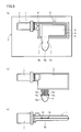
Fig. 1 (a)-(c) shows a resin encapsulation molding apparatus for an electrical circuit component according to a first embodiment.Fig. 1 (a) is a plan view schematically showing a mold surface of a bottom mold in the resin encapsulation molding apparatus.Fig. 1 (b) is a vertical cross sectional view taken along a line Ib-Ib inFig. 1 (a) and schematically showing a top mold and a bottom mold.Fig. 1 (c) is a vertical cross sectional view taken along a line Ic-Ic inFig. 1 (a) and schematically showing the bottom mold. -
Fig. 2 (a)-(b) is a vertical cross sectional view corresponding toFig. 1 (b) and schematically showing the top and bottom molds in the same embodiment.Fig. 2 (a) is a vertical cross sectional view showing a state in which the top and bottom molds are opened.Fig. 2 (b) is a vertical cross sectional view showing a state in which the top and bottom molds are opened. -
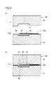
Fig. 3 (a)-(b) is a vertical cross sectional view taken along a line III-III inFig. 1 (a) and schematically showing the top and bottom molds in the same embodiment.Fig. 3 (a) is a vertical cross sectional view showing a state in which the top and bottom molds are opened.Fig. 3 (b) is a vertical cross sectional view showing a state in which the top and bottom molds are clamped together. -
Fig. 4 (a)-(b) is a vertical cross sectional view taken along a line Ic-Ic inFig. 1 (a) and schematically showing the top and bottom molds in the same embodiment.Fig. 4 (a) is a vertical cross sectional view showing a state in which the top and bottom molds are opened.Fig. 4 (b) is a vertical cross sectional view showing a state just before the top and bottom molds are clamped together. -
Fig. 5 (a)-(b) is a vertical cross sectional view corresponding toFig. 4 (b) and schematically showing the top and bottom molds in the same embodiment.Fig. 5 (a) is a first vertical cross sectional view for illustrating the step of arranging an external connection terminal at a predetermined position.Fig. 5 (b) is a second vertical cross sectional view for illustrating the step of arranging an external connection terminal at a predetermined position. -
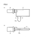
Fig. 6 (a)-(b) shows a resin encapsulation molded article encapsulating electrical circuit components with a resin material in the same embodiment.Fig. 6 (a) is a plan view of the resin encapsulation molded article.Fig. 6 (b) is a front view of the resin encapsulation molded article. -
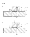
Fig. 7 (a)-(b) shows a resin encapsulation molding apparatus for an electrical circuit component according to a second embodiment.Fig. 7 (a) is a vertical cross sectional view corresponding toFig. 3 and showing a state in which the top and bottom molds are opened.Fig. 7 (b) is a vertical cross sectional view corresponding toFig. 3 showing a state in which the top and bottom molds are clamped together. -
Fig. 8 (a)-(c) is a diagram for illustrating the background art.Fig. 8 (a) is a plan view schematically showing a mold surface of a bottom mold in a resin encapsulation molding apparatus.Fig. 8 (b) is a plan view of a resin encapsulation molded article molded by the resin encapsulation molding apparatus.Fig. 8 (c) is a front view of the resin encapsulation molded article molded by the resin encapsulation molding apparatus. - A resin encapsulation molding apparatus according to a first embodiment of the present invention will be hereinafter described with reference to
Figs. 1-6 . -
Fig. 1 shows the main parts of a resin encapsulation molding apparatus for an electrical circuit component according to the first embodiment of the present invention. This resin encapsulation molding apparatus is equipped with a mold forresin molding 20 for encapsulating with a resin material and integrally molding electrical circuit components made up of a plurality of components that include a resin molded article (connector part) 10 and aglass epoxy substrate 40 and a metalexternal connection terminal 50 to be connected to a battery equipment which are electrically connected to the resin molded article. - A
bottom mold 21 in mold forresin molding 20 has a mold surface in which a cavity to be fitted with 30 to be fitted with the lower half of resin moldedarticle 10 and amolding cavity 60 to be fitted with the lower halves ofglass epoxy substrate 40 andexternal connection terminal 50 are provided. - In addition, the mold surface of
bottom mold 21 is provided with a guidingmember 70 for guiding resin moldedarticle 10 to a predetermined position in cavity to be fitted with 30 and a guidingmember 80 for guidingglass epoxy substrate 40 andexternal connection terminal 50 tomolding cavity 60. Guidingmember 70 has a taperedsurface 71 formed thereon. Guidingmember 80 has a taperedsurface 81 formed thereon. In this mold forresin molding 20, guidingmembers 70 are arranged at two points in front of and at the rear of cavity to be fitted with 30, respectively, while guidingmembers 80 are arranged at two points on the right and left ofexternal connection terminal 50 in a manner to adjoin opposing lateral surfaces of a tip end ofexternal connection terminal 50, respectively. - Further, the mold surface of
bottom mold 21 is provided with a pressing and supportingpart 90 to supportexternal connection terminal 50. Pressing and supportingpart 90 presses aconstricted portion 51, which is formed on each of the opposing lateral surfaces ofexternal connection terminal 50, against a fixingmember 91 provided at a predetermined position atbottom mold 21, thereby causing fixingmember 91 to supportexternal connection terminal 50. In this mold forresin molding 20, fixingmembers 91 are arranged at two points on the right and left onbottom mold 21 corresponding to the positions of right and left constrictedportions 51, respectively. - Above
bottom mold 21, atop mold 22 is arranged oppositebottom mold 21, as shown inFig. 1 (b) .Bottom mold 21 andtop mold 22 are arranged in a manner to enable opposing mold surfaces ofbottom mold 21 andtop mold 22 to be joined together (brought into contact) and separated from each other. It is noted that in a resin molding process, when a mold surface of a top mold and a mold surface of a bottom mold are joined together as shown inFig. 1 (b) , it is called "mold clamping". On the other hand, when the mold surface of the top mold and the mold surface the bottom mold are separated from each other (seeFig. 2 ), it is called "mold opening". - In a portion of the mold surface of
top mold 22 opposite cavity to be fitted with 30 ofbottom mold 21, a cavity to be fitted with 31 which is to be fitted with the upper half of resin moldedarticle 10 is provided. - Further, in a portion of the mold surface of
top mold 22opposite molding cavity 60 ofbottom mold 21, amolding cavity 61 which is to be fitted with the upper halves ofsubstrate 40 andexternal connection terminal 50 is provided. - Pressing and supporting
part 90 ofexternal connection terminal 50 is provided so that when each component of the electrical circuit components is integrally resin encapsulated to mold a resin encapsulation molded body encapsulating an electrical circuit component, it is prevented that a resin lump (seeresin lump 8a inFig. 8 ) is formed through adhesion of part of an encapsulating melted resin material (flowable resin) to constricted portions 51 (seeFig. 6 ) formed on the opposing lateral surfaces of anexternal connection terminal 50a which will protrude from the resin encapsulation molded body. - As shown in
Fig. 1 (c) , pressing and supportingpart 90 includes fixingmember 91 provided onbottom mold 21 and a pushing-out member 92 for pushingexternal connection terminal 50 out toward fixingmember 91. - As shown in
Fig. 1 (a) , fixingmember 91 is provided at a position to be fitted to constrictedportion 51 formed on each of the opposing lateral surfaces ofexternal connection terminal 50. In this case, fixingmembers 91 are provided at predetermined positions at two points on the right and left onbottom mold 21 in a manner to correspond to the respective positions of constrictedportions 51 at two points on the right and left ofexternal connection terminal 50. - Pushing-
out member 92 is arranged at a portion oftop mold 22 in the vicinity of the tip ofexternal connection terminal 50 arranged on the mold surface ofbottom mold 21. In this case, pushing-outmembers 92 are arranged at positions at two points on the right and left on the top mold. Further, pushing-out member 92 is arranged to be able to move vertically intop mold 22. In a state just beforebottom mold 21 andtop mold 22 are clamped together, pushing pushing-out member 92 down results in that a bottom surface portion of pushing-out member 92 adjoins the tip end ofexternal connection terminal 50, and atapered surface 92a formed on the bottom surface portion pushes the tip end ofexternal connection terminal 50 out toward fixingmember 91. - It is noted that at this time, the right and left opposing lateral surfaces of
external connection terminal 50 adjoin guidingmembers 80 arranged at two points on the right and left onbottom mold 21. This results in thatexternal connection terminal 50 is smoothly slid toward fixingmembers 91, under the guide of guidingmembers 80 on the right and left thereof. - As shown in
Fig. 1 (b) , cavity to be fitted with 30, 31 of mold forresin molding 20 is provided with aprotrusion pin 23.Molding cavity protrusion pin 24. - In resin encapsulation molding, the component fitted into cavity to be fitted with 30, 31 is held at a predetermined height (position) by causing a tip end portion of
protrusion pin 23 to protrude into cavity to be fitted with 30, 31, while the component fitted intomolding cavity protrusion pin 24 to protrude intomolding cavity - It is noted with this mold for resin molding, pushing-
out member 92 of pressing and supportingparts 90 is shown as being arranged in a symmetrical pair (a multiple arrangement) on thetop mold 22 at positions in front of right and left guidingmembers 80 provided atbottom mold 21. As the pushing-out member, one (single) pushing-out member may be provided, which is configured such that pushing the pushing-out member down results in that a bottom surface portion of the pushing-out member adjoins the tip end of the external connection terminal, and a tapered surface formed on the bottom surface portion pushes the tip end of external connection terminal out toward the fixing member. - Next, referring to
Figs. 2-6 , description will be given on a method of molding a resin encapsulation molded article (product) encapsulating an electrical circuit component, using the above-described mold for resin molding. - First, resin molded article (connector part) 10 is fitted into cavity to be fitted with 30 provided in the mold surface of
bottom mold 21 of mold forresin molding 20, andglass epoxy substrate 40 andexternal connection terminal 50 are fitted into molding cavity 60 (the step of fitting a plurality of components). - In this step, as shown in
Fig. 2 (a) , a plurality of components may be introduced between openedtop mold 22 andbottom mold 21 automatically with any suitable carrying device or manually. - The guiding member provided at the mold for resin molding then guides the resin molded article to a predetermined position in the cavity to be fitted with and guides the substrate and the external connection terminal to the molding cavity (the step of assisting the fitting of a plurality of components). It is noted that this step may be performed simultaneously with the step of fitting a plurality of components.
- Tapered
surface 71 of guidingmember 70 provided atbottom mold 21 fits resin moldedarticle 10 into cavity to be fitted with 30 and guides the lower half of resin moldedarticle 10 to a predetermined position in cavity to be fitted with 30. - Tapered
surface 81 of guidingmember 80 provided atbottom mold 21 fitsexternal connection terminal 50 intomolding cavity 60 and guides the lower half ofexternal connection terminal 50 to a predetermined position inmolding cavity 60. - Here, if the structure of
glass epoxy substrate 40 is one in which it is integrally connected toexternal connection terminal 50, then the above-described step of assisting the fitting ofexternal connection terminal 50 causesglass epoxy substrate 40 to have its lower half fitted intomolding cavity 60. - In contrast, if the structure of
glass epoxy substrate 40 andexternal connection terminal 50 is one in which they are electrically connected but not made into one piece, then fitting resin moldedarticle 10 into cavity to be fitted with 30 and fittingexternal connection terminal 50 intomolding cavity 60 causeglass epoxy substrate 40 andexternal connection terminal 50 to sequentially have their respective lower halves fitted intomolding cavity 60. - In fitting the lower half of
external connection terminal 50 intomolding cavity 60, as shown inFig. 1 (a) , two constrictedportions external connection terminal 50 enter a state of being fitted with two fixingmembers -
External connection terminal 50 is then guided to a predetermined position, and two constrictedportions external connection terminal 50 are pressed against two fixingmembers external connection terminal 50 is supported by fixingmembers 91, 91 (the step of pressing and supporting an external connection terminal). - In the step of assisting the fitting of a plurality of components, as shown in
Fig. 4 (a) , two constrictedportions external connection terminal 50 are in a state of being fitted with two fixingmembers - In this state, as shown in
Fig. 4 (b) ,top mold 22 is lowered to a position H at which the mold surface oftop mold 22 and the mold surface ofbottom mold 21 are just before being joined together, i.e. mold clamping. At this time,external connection terminal 50 is not under any mold clamping pressure applied by the top mold and the bottom mold. Thus, pushing pushing-out member 92 down in this state results in that the bottom surface portion of the pushing-out member adjoins the tip end ofexternal connection terminal 50, and taperedsurface 92a formed on the bottom surface portion pushesexternal connection terminal 50 out toward fixingmember 91, as shown inFig. 5 (a) . - This results in that
external connection terminal 50 smoothly slides toward fixingmember 91, under the guide of right and left guidingmembers 80 provided atbottom mold 21 and that right and left constrictedportions 51 ofexternal connection terminal 50 are pressed by right and left fixingmembers 91 provided atbottom mold 21. In this way,external connection terminal 50 is supported by fixingmember 91. - The mold surface of
top mold 22 and the mold surface ofbottom mold 21 are then joined together (the step of clamping molds).Glass epoxy substrate 40 andexternal connection terminal 50 are then encapsulated with a resin material, and the resin material encapsulatingglass epoxy substrate 40 and the like are molded (the step of resin encapsulation molding a substrate and an external connection terminal). A thermosetting melted resin material (flowable resin) R is injected intomolding cavity 60, 61 (seeFig. 1 (a) ) and fillsmolding cavity glass epoxy substrate 40 andexternal connection terminal 50 which are fitted into the molding cavity, and the encapsulating resin material is molded. Through this step, a resin encapsulation molded body (solidified resin) encapsulatingglass epoxy substrate 40 andexternal connection terminal 50 is formed, and the resin encapsulation molded body and resin molded article (connector part) 10 are connected integrally together, so that a resin encapsulation molded article is formed. - The mold surface of
top mold 22 and the mold surface ofbottom mold 21 are then separated from each other (the step of opening molds). The resin encapsulation molded article encapsulating an electrical circuit component is then removed from betweentop mold 22 and bottom mold 21 (the step of removing a product). - As shown in
Fig. 6 , in the resin encapsulation molded article encapsulating an electrical circuit component removed from the mold for resin molding, resin molded article (connector part) 10 and a resin encapsulation moldedbody 77 encapsulating the glass epoxy substrate and the external connection terminal are integrally connected together, so that they are made into one piece. - No resin lump or resin flash is formed on two constricted
portions body 77. - This is due to the facts in the step of resin encapsulation molding that
external connection terminal 50 is supported by fixingmember 91 with two constrictedportions members bottom mold 21 and that under a mold clamping pressure applied bytop mold 22 andbottom mold 21, the upper surface ofterminal 50a is in close contact with the mold surface oftop mold 22 and the lower surface ofterminal 50a is in close contact with the mold surface ofbottom mold 21. - According to the above-described first embodiment, even in a case where each component of electrical circuit components including connector part (resin molded article) 10 and
glass epoxy substrate 40 and metalexternal connection terminal 50 which are electrically connected to the connector part are directly fitted into a predetermined cavity (cavity to be fitted with, molding cavity) of mold forresin molding 20, it is ensured, without use of a lead frame, that each component is fitted into a predetermined cavity and arranged at a predetermined position. This allows to ensure that mold forresin molding 20 is clamped. Thus, it is prevented that part of a melted resin material flows out of the mold surface of the mold for resin molding to the outside of the cavity. As a result, a resin flash is efficiently and reliably prevented from being formed onconstricted portion 51 of and a surface of terminal 50a which protrudes from resin encapsulation molded body of the resin encapsulation molded article. - Next, referring to
Fig. 7 , a resin encapsulation molding apparatus according to a second embodiment of the present invention will be described. - The resin encapsulation molding apparatus according to the second embodiment has a structure which can further ensure that a resin flash is prevented from being formed on a surface of
terminal 50a protruding from resin encapsulation moldedbody 77. It is noted that to avoid redundancy in the description, same members as those of the above-described resin encapsulation molding apparatus have the same reference characters allotted inFig. 7 . - Once the top mold and the bottom mold are clamped together, the tip end of
external connection terminal 50, which is not fitted intomolding cavity top mold 22 andbottom mold 21, will be sandwiched between the mold surface of the top mold and the mold surface of the bottom mold, under a mold clamping pressure. As a result, after resin molding, the tip end of external connection terminal serves as terminal 50a for external connection which protrudes from resin encapsulating molded body 77 (seeFig. 6 ). - At this time, when the tip end of
connection terminal 50 is under an appropriate mold clamping pressure applied by the top mold and the bottom mold, it can be prevented that a resin flash is formed through adhesion of part of a melted resin material (flowable resin) to a surface ofterminal 50a. However,external connection terminal 50 varies in thickness. For this reason, for example, when the external connection terminal has a thickness less than a predetermined thickness, in clamping the top mold and the bottom mold together, a gap may develop between the tip end of the external connection terminal and the mold surface of the top mold or the mold surface of the bottom mold. If so, this gap may cause a resin flash to be formed through adhesion of part of the molten resin material to a surface ofterminal 50a. - In the resin encapsulation molding apparatus according to the second embodiment, a resin flash adhesion preventing part having a pressing member is provided so that in clamping
top mold 22 andbottom mold 21 together, no gap develops between a surface ofterminal 50a protruding from resin encapsulation moldedbody 77 and the mold surface oftop mold 22 or the mold surface ofbottom mold 21. By bringing a pressing surface of the pressing member into contact with a surface of terminal 50a by means of elastic force, it can be prevented that part of a melted resin material adheres to the surface ofterminal 50a. - As shown in
Fig. 7 , the resin flashadhesion preventing part 93 includes thepressing member 93a fitted intotop mold 22 in a vertically movable manner and anelastic member 93b. Pressingmember 93a is pushed out downward because of the elasticity ofelastic member 93b. In clampingtop mold 22 andbottom mold 21 together, apressing surface 93c provided on the bottom end surface of pressingmember 93a comes into contact with a surface (upper surface) ofterminal 50a arranged onbottom mold 21, by means of elastic force. - It is noted that although
Fig. 7 shows the resin encapsulation molding apparatus in which resin flashadhesion preventing part 93 is provided only attop mold 22, a resin flash adhesion preventing part having the same functions may also be provided atbottom mold 21. In this case, in clampingtop mold 22 andbottom mold 21 together, pressing surfaces of the pressing members come into contact with the front surface (upper surface) and the back surface (lower surface) ofterminal 50a, respectively, by means of elastic force. - With the resin encapsulation molding apparatus according to the second embodiment, pressing
surface 93c of pressingmember 93a comes into contact with a surface of terminal 50a by means of elastic force just beforetop mold 22 andbottom mold 21 are clamped together (the step of preventing adhesion of a resin flash). - This allows to further ensure that a resin flash is prevented from being formed through adhesion of part of a melted resin material to a surface of
terminal 50a protruding from resin encapsulating moldedbody 77. - While the description has been given on a case where a thermosetting resin material is used as a resin material in each embodiment above, a thermoplastic resin material may be employed.
- In addition, as a resin material, resin materials in various shapes such as a granular resin material (granular resin), a liquid resin material (liquid resin), a powdered resin material having a prescribed particle size distribution (powdered resin), a powdery resin material (powdery resin), a pasty resin material (pasty resin), a tablet resin material (tablet resin), or the like can be employed.
- Further, an epoxy-based resin material (epoxy resin) or a silicon-based resin material (silicon resin) may be employed as a resin material.
- Further, in each embodiment above, as a technique for injecting flowable resin R into
molding cavity - When using a transfer molding, a resin tablet (epoxy-based resin material) supplied into a pot is heated to melt. By applying pressure to the melted resin material (flowable resin) with a plunger fitted into the pot, the melted resin material is injected via a resin path (a cull part, a runner, a gate) into
molding cavity - After expiration of a predetermined period of time required for the melted resin material to set, a mold for resin molding (a top mold, a bottom mold) can be opened, thereby providing a resin encapsulation molded article encapsulating an electrical circuit component.
- The present invention is not limited to the embodiments described above and can be employed in any appropriate combination, modification or selection as necessary without departing from the spirit and the scope of the present invention.
- Although the present invention has been described and illustrated in detail, it is clearly understood that the same is by way of illustration and example only and is not to be taken by way of limitation, the scope of the present invention being interpreted by the terms of the appended claims.
Claims (5)
- A resin encapsulation molding method for an electrical circuit component to encapsulate, with a resin material (R), a plurality of electrical circuit components that include a resin molded article (10) and a substrate (40) and an external connection terminal (50) electrically connected to said resin molded article (10), and to mold encapsulating said resin material (R), the method comprising the steps of:fitting said resin molded article (10) into a cavity to be fitted with (30, 31) provided in a mold surface of a mold for resin molding (20) and fitting said substrate (40) and said external connection terminal (50) into a molding cavity (60, 61) provided in the mold surface of said mold for resin molding (20);guiding said resin molded article (10) to a predetermined position in said cavity to be fitted with (30, 31) by means of a first guiding member (70) provided at said mold for resin molding (20) and guiding said substrate (40) and said external connection terminal (50) to said molding cavity (60, 61) by means of a second guiding member (80) provided at said mold for resin molding (20);causing a fixing member (91) provided at said mold for resin molding (20) to support said external connection terminal (50), by guiding said external connection terminal (50) to a predetermined position in said mold for resin molding (20) and by pressing a constricted portion (51) formed on a lateral surface of said external connection terminal (50) against said fixing member (91);clamping said mold for resin molding (20);encapsulating said substrate (40) and said external connection terminal (50) fitted into said molding cavity (60, 61), by injecting said resin material (R) into said molding cavity (60, 61) formed by the mold clamping of said mold for resin molding (20) to fill said molding cavity (60, 61);molding said resin material (R) encapsulating said substrate (40) and said external connection terminal (50) in a manner to form a resin encapsulation molded body (77) encapsulating said substrate (40) and said external connection terminal (50) to integrally connect said resin encapsulation molded body (77) and said resin molded article (10) together and to make said resin encapsulation molded body (77) and said resin molded article (10) into one piece so that a resin encapsulation molded article (10, 77) is formed; andopening said mold for resin molding (20) and removing, from said mold for resin molding (20), said resin encapsulation molded body (77) and said resin molded article (10) that have been made into one piece.
- The resin encapsulation molding method for an electrical circuit component according to claim 1, wherein
clamping said mold for resin molding (20) includes bringing a pressing surface of a pressing member (93) provided at said mold for resin molding (20) into contact with a surface of said external connection terminal (50), by means of elastic force. - A resin encapsulation molding apparatus for an electrical circuit component to encapsulate, with a resin material (R), a plurality of electrical circuit components that include a resin molded article (10) and a substrate (40) and an external connection terminal (50) electrically connected to said resin molded article (10), and to mold encapsulating said resin material (R), the apparatus being equipped with a mold for resin molding (20),
said mold for resin molding (20) comprising:a cavity to be fitted with (30, 31) to be fitted with said resin molded article (10);a molding cavity (60, 61) to be fitted with said substrate (40) and said external connection terminal (50);a first guiding member (70) to guide said resin molded article (10) to a predetermined position in said cavity to be fitted with (30, 31);a second guiding member (80) to guide said substrate (40) and said external connection terminal (50) to said molding cavity (60, 61); anda pressing and supporting part (90) including a fixing member (91) and to cause said fixing member (91) to support said external connection terminal (50) by pressing a constricted portion (51) formed on a lateral surface of said external connection terminal (50) against said fixing member (91). - The resin encapsulation molding apparatus for an electrical circuit component according to claim 3, wherein
said mold for resin molding (20) comprises a first pressing member (93) having a pressing surface which comes into contact with a surface of said external connection terminal (50) by means of elastic force. - The resin encapsulation molding apparatus for an electrical circuit component according to claim 4, wherein
said mold for resin molding (20) comprises a second pressing member having a pressing surface which comes into contact with a back surface of said external connection terminal (50) by means of elastic force.
Applications Claiming Priority (1)
| Application Number | Priority Date | Filing Date | Title |
|---|---|---|---|
| JP2010245906A JP5385886B2 (en) | 2010-11-02 | 2010-11-02 | Resin sealing molding method and apparatus for electric circuit parts |
Publications (2)
| Publication Number | Publication Date |
|---|---|
| EP2447986A1 true EP2447986A1 (en) | 2012-05-02 |
| EP2447986B1 EP2447986B1 (en) | 2014-06-04 |
Family
ID=45001640
Family Applications (1)
| Application Number | Title | Priority Date | Filing Date |
|---|---|---|---|
| EP11186409.6A Active EP2447986B1 (en) | 2010-11-02 | 2011-10-24 | Resin encapsulation molding method and apparatus for electrical circuit component |
Country Status (4)
| Country | Link |
|---|---|
| EP (1) | EP2447986B1 (en) |
| JP (1) | JP5385886B2 (en) |
| KR (1) | KR101311027B1 (en) |
| CN (1) | CN102463653B (en) |
Cited By (1)
| Publication number | Priority date | Publication date | Assignee | Title |
|---|---|---|---|---|
| DE102019121229A1 (en) * | 2019-08-06 | 2021-02-11 | Infineon Technologies Ag | Electronic devices with electrically isolated load electrodes |
Families Citing this family (6)
| Publication number | Priority date | Publication date | Assignee | Title |
|---|---|---|---|---|
| WO2013136926A1 (en) * | 2012-03-16 | 2013-09-19 | 株式会社村田製作所 | Device for producing sealing resin sheet and method for producing sealing resin sheet |
| CN102738020A (en) * | 2012-06-26 | 2012-10-17 | 铜陵三佳山田科技有限公司 | Integrated circuit plastic packaging mold for preventing horizontal overflowed material at cored hole |
| JP6804410B2 (en) * | 2017-08-09 | 2020-12-23 | Towa株式会社 | Conveying mechanism, resin molding device, method of delivering the object to be molded to the molding mold, and method of manufacturing the resin molded product |
| US11145966B2 (en) * | 2019-08-28 | 2021-10-12 | Pctel, Inc. | Over-molded thin film antenna device |
| CN114889039A (en) * | 2022-04-19 | 2022-08-12 | 微智医疗器械有限公司 | Retina implant flexible electrode, encapsulation mold and encapsulation method thereof |
| CN117207442A (en) * | 2023-11-09 | 2023-12-12 | 成都宝利根创科电子有限公司 | Terminal in-mold forming method |
Citations (6)
| Publication number | Priority date | Publication date | Assignee | Title |
|---|---|---|---|---|
| EP0257681A2 (en) * | 1986-08-27 | 1988-03-02 | STMicroelectronics S.r.l. | Method for manufacturing plastic encapsulated semiconductor devices and devices obtained thereby |
| US5384286A (en) * | 1991-08-16 | 1995-01-24 | Mitsubishi Denki Kabushiki Kaisha | Process for encapsulating a semiconductor chip, leadframe and heatsink |
| JP2003037241A (en) | 2001-07-24 | 2003-02-07 | Hitachi Ltd | Electrical circuit board package item and manufacturing method for the electric circuit board package item |
| US20030180985A1 (en) * | 2002-03-20 | 2003-09-25 | Mitsubishi Denki Kabushiki Kaisha | Method for manufacturing a semiconductor device and a resin sealing device therefor |
| US20040166605A1 (en) * | 2002-10-10 | 2004-08-26 | Bunshi Kuratomi | Fabrication method of semiconductor integrated circuit device |
| WO2010038660A1 (en) * | 2008-09-30 | 2010-04-08 | Towa株式会社 | Resin sealing compression molding method for electronic component and device therefor |
Family Cites Families (8)
| Publication number | Priority date | Publication date | Assignee | Title |
|---|---|---|---|---|
| JPH0831489B2 (en) * | 1987-07-20 | 1996-03-27 | サンケン電気株式会社 | Method for manufacturing resin-sealed electric component |
| JP3397741B2 (en) * | 2000-03-07 | 2003-04-21 | Towa株式会社 | Substrate positioning mechanism and positioning method |
| JP4153862B2 (en) * | 2003-10-24 | 2008-09-24 | 第一精工株式会社 | Mold for semiconductor resin sealing |
| JP2007095804A (en) * | 2005-09-27 | 2007-04-12 | Towa Corp | Method and apparatus for forming resin sealing of electronic component |
| JP4084844B2 (en) * | 2005-09-27 | 2008-04-30 | Towa株式会社 | Resin sealing molding method and apparatus for electronic parts |
| JP2007281364A (en) * | 2006-04-11 | 2007-10-25 | Towa Corp | Resin sealing and molding method and apparatus for electronic component |
| JP2009124012A (en) * | 2007-11-16 | 2009-06-04 | Towa Corp | Compression molding method of electronic component, and die |
| JP5056717B2 (en) * | 2008-10-16 | 2012-10-24 | 株式会社デンソー | Mold package manufacturing method |
-
2010
- 2010-11-02 JP JP2010245906A patent/JP5385886B2/en active Active
-
2011
- 2011-10-24 EP EP11186409.6A patent/EP2447986B1/en active Active
- 2011-10-26 KR KR1020110109710A patent/KR101311027B1/en active IP Right Grant
- 2011-11-02 CN CN201110344139.4A patent/CN102463653B/en active Active
Patent Citations (6)
| Publication number | Priority date | Publication date | Assignee | Title |
|---|---|---|---|---|
| EP0257681A2 (en) * | 1986-08-27 | 1988-03-02 | STMicroelectronics S.r.l. | Method for manufacturing plastic encapsulated semiconductor devices and devices obtained thereby |
| US5384286A (en) * | 1991-08-16 | 1995-01-24 | Mitsubishi Denki Kabushiki Kaisha | Process for encapsulating a semiconductor chip, leadframe and heatsink |
| JP2003037241A (en) | 2001-07-24 | 2003-02-07 | Hitachi Ltd | Electrical circuit board package item and manufacturing method for the electric circuit board package item |
| US20030180985A1 (en) * | 2002-03-20 | 2003-09-25 | Mitsubishi Denki Kabushiki Kaisha | Method for manufacturing a semiconductor device and a resin sealing device therefor |
| US20040166605A1 (en) * | 2002-10-10 | 2004-08-26 | Bunshi Kuratomi | Fabrication method of semiconductor integrated circuit device |
| WO2010038660A1 (en) * | 2008-09-30 | 2010-04-08 | Towa株式会社 | Resin sealing compression molding method for electronic component and device therefor |
Cited By (2)
| Publication number | Priority date | Publication date | Assignee | Title |
|---|---|---|---|---|
| DE102019121229A1 (en) * | 2019-08-06 | 2021-02-11 | Infineon Technologies Ag | Electronic devices with electrically isolated load electrodes |
| US11646258B2 (en) | 2019-08-06 | 2023-05-09 | Infineon Technologies Ag | Electronic devices including electrically insulated load electrodes |
Also Published As
| Publication number | Publication date |
|---|---|
| JP2012099628A (en) | 2012-05-24 |
| CN102463653A (en) | 2012-05-23 |
| KR20120046684A (en) | 2012-05-10 |
| JP5385886B2 (en) | 2014-01-08 |
| CN102463653B (en) | 2014-09-17 |
| KR101311027B1 (en) | 2013-09-24 |
| EP2447986B1 (en) | 2014-06-04 |
Similar Documents
| Publication | Publication Date | Title |
|---|---|---|
| EP2447986A1 (en) | Resin encapsulation molding method and apparatus for electrical circuit component | |
| US8202457B2 (en) | Method and apparatus for producing battery pack | |
| KR101006621B1 (en) | Electronic circuit device and method of making the same | |
| US8300419B2 (en) | Electronic circuit device and method of making the same | |
| CN108028235B (en) | Resin sealing device and resin sealing method | |
| JP6320172B2 (en) | Resin sealing method and resin sealing device for electronic parts | |
| KR960700875A (en) | Resin encapsulation method of semiconductor device | |
| CN109383047B (en) | Resin molding device and method for manufacturing resin molded product | |
| JPH03202327A (en) | Cleaning process of mold face for molding resin, sheet member for cleaning used in same process and continuous automatic resin-molding process | |
| KR102259426B1 (en) | Compression molding apparatus, compression molding method, and manufacturing method of compression molded products | |
| JPH0976282A (en) | Resin seal molding method for electric and electronic parts and tool used therefor | |
| US20220293434A1 (en) | Semiconductor manufacturing apparatus and method of manufacturing semiconductor device using the same, and semiconductor device | |
| US6682952B2 (en) | Method of forming the resin sealed semiconductor device using the lead frame | |
| US8122592B2 (en) | Method for producing a low-current switch module comprising electrical components | |
| TWI778332B (en) | Resin molding apparatus and method for producing resin molded product | |
| TW421868B (en) | Device and method for encapsulating electronic component mounted on a carrier | |
| JP2010149423A (en) | Transfer molding mold and method for manufacturing semiconductor device | |
| JP2004311855A (en) | Mold for resin seal molding of electronic part | |
| JP6861507B2 (en) | Compression molding equipment, compression molding method, and manufacturing method of compression molded products | |
| JP5723800B2 (en) | Compressed resin sealing molding method and apparatus for semiconductor chip | |
| CN102157822B (en) | Electrical connecting component comprosing a hotmelt element, method and tool for manufacturing such an electrical component | |
| GB2054447A (en) | Encapsulating semiconductor devices by injection moulding | |
| JPH01216815A (en) | Transfer resin encapsulation molding of component to be encapsulated, resin encapsulation mold assembly used therefor and film carrier | |
| JP3795684B2 (en) | Resin sealing molding method for electronic parts | |
| JP3795670B2 (en) | Resin sealing molding method for electronic parts |
Legal Events
| Date | Code | Title | Description |
|---|---|---|---|
| PUAI | Public reference made under article 153(3) epc to a published international application that has entered the european phase |
Free format text: ORIGINAL CODE: 0009012 |
|
| AK | Designated contracting states |
Kind code of ref document: A1 Designated state(s): AL AT BE BG CH CY CZ DE DK EE ES FI FR GB GR HR HU IE IS IT LI LT LU LV MC MK MT NL NO PL PT RO RS SE SI SK SM TR |
|
| AX | Request for extension of the european patent |
Extension state: BA ME |
|
| 17P | Request for examination filed |
Effective date: 20120613 |
|
| RIC1 | Information provided on ipc code assigned before grant |
Ipc: H01L 23/31 20060101ALI20130715BHEP Ipc: B29C 45/14 20060101ALI20130715BHEP Ipc: H01L 21/56 20060101AFI20130715BHEP Ipc: H01L 21/67 20060101ALI20130715BHEP |
|
| 17Q | First examination report despatched |
Effective date: 20130808 |
|
| GRAP | Despatch of communication of intention to grant a patent |
Free format text: ORIGINAL CODE: EPIDOSNIGR1 |
|
| INTG | Intention to grant announced |
Effective date: 20140116 |
|
| GRAS | Grant fee paid |
Free format text: ORIGINAL CODE: EPIDOSNIGR3 |
|
| GRAA | (expected) grant |
Free format text: ORIGINAL CODE: 0009210 |
|
| AK | Designated contracting states |
Kind code of ref document: B1 Designated state(s): AL AT BE BG CH CY CZ DE DK EE ES FI FR GB GR HR HU IE IS IT LI LT LU LV MC MK MT NL NO PL PT RO RS SE SI SK SM TR |
|
| REG | Reference to a national code |
Ref country code: GB Ref legal event code: FG4D |
|
| REG | Reference to a national code |
Ref country code: CH Ref legal event code: EP |
|
| REG | Reference to a national code |
Ref country code: AT Ref legal event code: REF Ref document number: 671508 Country of ref document: AT Kind code of ref document: T Effective date: 20140615 |
|
| REG | Reference to a national code |
Ref country code: IE Ref legal event code: FG4D |
|
| REG | Reference to a national code |
Ref country code: DE Ref legal event code: R096 Ref document number: 602011007384 Country of ref document: DE Effective date: 20140717 |
|
| REG | Reference to a national code |
Ref country code: AT Ref legal event code: MK05 Ref document number: 671508 Country of ref document: AT Kind code of ref document: T Effective date: 20140604 |
|
| REG | Reference to a national code |
Ref country code: NL Ref legal event code: VDEP Effective date: 20140604 |
|
| PG25 | Lapsed in a contracting state [announced via postgrant information from national office to epo] |
Ref country code: LT Free format text: LAPSE BECAUSE OF FAILURE TO SUBMIT A TRANSLATION OF THE DESCRIPTION OR TO PAY THE FEE WITHIN THE PRESCRIBED TIME-LIMIT Effective date: 20140604 Ref country code: FI Free format text: LAPSE BECAUSE OF FAILURE TO SUBMIT A TRANSLATION OF THE DESCRIPTION OR TO PAY THE FEE WITHIN THE PRESCRIBED TIME-LIMIT Effective date: 20140604 Ref country code: CY Free format text: LAPSE BECAUSE OF FAILURE TO SUBMIT A TRANSLATION OF THE DESCRIPTION OR TO PAY THE FEE WITHIN THE PRESCRIBED TIME-LIMIT Effective date: 20140604 Ref country code: GR Free format text: LAPSE BECAUSE OF FAILURE TO SUBMIT A TRANSLATION OF THE DESCRIPTION OR TO PAY THE FEE WITHIN THE PRESCRIBED TIME-LIMIT Effective date: 20140905 Ref country code: NO Free format text: LAPSE BECAUSE OF FAILURE TO SUBMIT A TRANSLATION OF THE DESCRIPTION OR TO PAY THE FEE WITHIN THE PRESCRIBED TIME-LIMIT Effective date: 20140904 |
|
| REG | Reference to a national code |
Ref country code: LT Ref legal event code: MG4D |
|
| PG25 | Lapsed in a contracting state [announced via postgrant information from national office to epo] |
Ref country code: SE Free format text: LAPSE BECAUSE OF FAILURE TO SUBMIT A TRANSLATION OF THE DESCRIPTION OR TO PAY THE FEE WITHIN THE PRESCRIBED TIME-LIMIT Effective date: 20140604 Ref country code: AT Free format text: LAPSE BECAUSE OF FAILURE TO SUBMIT A TRANSLATION OF THE DESCRIPTION OR TO PAY THE FEE WITHIN THE PRESCRIBED TIME-LIMIT Effective date: 20140604 Ref country code: LV Free format text: LAPSE BECAUSE OF FAILURE TO SUBMIT A TRANSLATION OF THE DESCRIPTION OR TO PAY THE FEE WITHIN THE PRESCRIBED TIME-LIMIT Effective date: 20140604 Ref country code: RS Free format text: LAPSE BECAUSE OF FAILURE TO SUBMIT A TRANSLATION OF THE DESCRIPTION OR TO PAY THE FEE WITHIN THE PRESCRIBED TIME-LIMIT Effective date: 20140604 Ref country code: HR Free format text: LAPSE BECAUSE OF FAILURE TO SUBMIT A TRANSLATION OF THE DESCRIPTION OR TO PAY THE FEE WITHIN THE PRESCRIBED TIME-LIMIT Effective date: 20140604 |
|
| REG | Reference to a national code |
Ref country code: HU Ref legal event code: AG4A Ref document number: E021515 Country of ref document: HU |
|
| PG25 | Lapsed in a contracting state [announced via postgrant information from national office to epo] |
Ref country code: CZ Free format text: LAPSE BECAUSE OF FAILURE TO SUBMIT A TRANSLATION OF THE DESCRIPTION OR TO PAY THE FEE WITHIN THE PRESCRIBED TIME-LIMIT Effective date: 20140604 Ref country code: ES Free format text: LAPSE BECAUSE OF FAILURE TO SUBMIT A TRANSLATION OF THE DESCRIPTION OR TO PAY THE FEE WITHIN THE PRESCRIBED TIME-LIMIT Effective date: 20140604 Ref country code: PT Free format text: LAPSE BECAUSE OF FAILURE TO SUBMIT A TRANSLATION OF THE DESCRIPTION OR TO PAY THE FEE WITHIN THE PRESCRIBED TIME-LIMIT Effective date: 20141006 Ref country code: RO Free format text: LAPSE BECAUSE OF FAILURE TO SUBMIT A TRANSLATION OF THE DESCRIPTION OR TO PAY THE FEE WITHIN THE PRESCRIBED TIME-LIMIT Effective date: 20140604 Ref country code: SK Free format text: LAPSE BECAUSE OF FAILURE TO SUBMIT A TRANSLATION OF THE DESCRIPTION OR TO PAY THE FEE WITHIN THE PRESCRIBED TIME-LIMIT Effective date: 20140604 Ref country code: EE Free format text: LAPSE BECAUSE OF FAILURE TO SUBMIT A TRANSLATION OF THE DESCRIPTION OR TO PAY THE FEE WITHIN THE PRESCRIBED TIME-LIMIT Effective date: 20140604 |
|
| PG25 | Lapsed in a contracting state [announced via postgrant information from national office to epo] |
Ref country code: NL Free format text: LAPSE BECAUSE OF FAILURE TO SUBMIT A TRANSLATION OF THE DESCRIPTION OR TO PAY THE FEE WITHIN THE PRESCRIBED TIME-LIMIT Effective date: 20140604 Ref country code: IS Free format text: LAPSE BECAUSE OF FAILURE TO SUBMIT A TRANSLATION OF THE DESCRIPTION OR TO PAY THE FEE WITHIN THE PRESCRIBED TIME-LIMIT Effective date: 20141004 Ref country code: PL Free format text: LAPSE BECAUSE OF FAILURE TO SUBMIT A TRANSLATION OF THE DESCRIPTION OR TO PAY THE FEE WITHIN THE PRESCRIBED TIME-LIMIT Effective date: 20140604 |
|
| REG | Reference to a national code |
Ref country code: DE Ref legal event code: R097 Ref document number: 602011007384 Country of ref document: DE |
|
| PLBE | No opposition filed within time limit |
Free format text: ORIGINAL CODE: 0009261 |
|
| STAA | Information on the status of an ep patent application or granted ep patent |
Free format text: STATUS: NO OPPOSITION FILED WITHIN TIME LIMIT |
|
| PG25 | Lapsed in a contracting state [announced via postgrant information from national office to epo] |
Ref country code: IT Free format text: LAPSE BECAUSE OF FAILURE TO SUBMIT A TRANSLATION OF THE DESCRIPTION OR TO PAY THE FEE WITHIN THE PRESCRIBED TIME-LIMIT Effective date: 20140604 Ref country code: DK Free format text: LAPSE BECAUSE OF FAILURE TO SUBMIT A TRANSLATION OF THE DESCRIPTION OR TO PAY THE FEE WITHIN THE PRESCRIBED TIME-LIMIT Effective date: 20140604 |
|
| 26N | No opposition filed |
Effective date: 20150305 |
|
| PG25 | Lapsed in a contracting state [announced via postgrant information from national office to epo] |
Ref country code: LU Free format text: LAPSE BECAUSE OF FAILURE TO SUBMIT A TRANSLATION OF THE DESCRIPTION OR TO PAY THE FEE WITHIN THE PRESCRIBED TIME-LIMIT Effective date: 20141024 Ref country code: MC Free format text: LAPSE BECAUSE OF FAILURE TO SUBMIT A TRANSLATION OF THE DESCRIPTION OR TO PAY THE FEE WITHIN THE PRESCRIBED TIME-LIMIT Effective date: 20140604 |
|
| REG | Reference to a national code |
Ref country code: CH Ref legal event code: PL |
|
| REG | Reference to a national code |
Ref country code: DE Ref legal event code: R097 Ref document number: 602011007384 Country of ref document: DE Effective date: 20150305 |
|
| REG | Reference to a national code |
Ref country code: IE Ref legal event code: MM4A |
|
| PG25 | Lapsed in a contracting state [announced via postgrant information from national office to epo] |
Ref country code: LI Free format text: LAPSE BECAUSE OF NON-PAYMENT OF DUE FEES Effective date: 20141031 Ref country code: SI Free format text: LAPSE BECAUSE OF FAILURE TO SUBMIT A TRANSLATION OF THE DESCRIPTION OR TO PAY THE FEE WITHIN THE PRESCRIBED TIME-LIMIT Effective date: 20140604 Ref country code: CH Free format text: LAPSE BECAUSE OF NON-PAYMENT OF DUE FEES Effective date: 20141031 |
|
| REG | Reference to a national code |
Ref country code: FR Ref legal event code: ST Effective date: 20150630 |
|
| PG25 | Lapsed in a contracting state [announced via postgrant information from national office to epo] |
Ref country code: FR Free format text: LAPSE BECAUSE OF NON-PAYMENT OF DUE FEES Effective date: 20141031 |
|
| PG25 | Lapsed in a contracting state [announced via postgrant information from national office to epo] |
Ref country code: IE Free format text: LAPSE BECAUSE OF NON-PAYMENT OF DUE FEES Effective date: 20141024 |
|
| PG25 | Lapsed in a contracting state [announced via postgrant information from national office to epo] |
Ref country code: SM Free format text: LAPSE BECAUSE OF FAILURE TO SUBMIT A TRANSLATION OF THE DESCRIPTION OR TO PAY THE FEE WITHIN THE PRESCRIBED TIME-LIMIT Effective date: 20140604 |
|
| GBPC | Gb: european patent ceased through non-payment of renewal fee |
Effective date: 20151024 |
|
| PG25 | Lapsed in a contracting state [announced via postgrant information from national office to epo] |
Ref country code: BG Free format text: LAPSE BECAUSE OF FAILURE TO SUBMIT A TRANSLATION OF THE DESCRIPTION OR TO PAY THE FEE WITHIN THE PRESCRIBED TIME-LIMIT Effective date: 20140604 |
|
| PG25 | Lapsed in a contracting state [announced via postgrant information from national office to epo] |
Ref country code: GB Free format text: LAPSE BECAUSE OF NON-PAYMENT OF DUE FEES Effective date: 20151024 Ref country code: MT Free format text: LAPSE BECAUSE OF FAILURE TO SUBMIT A TRANSLATION OF THE DESCRIPTION OR TO PAY THE FEE WITHIN THE PRESCRIBED TIME-LIMIT Effective date: 20140604 Ref country code: BE Free format text: LAPSE BECAUSE OF FAILURE TO SUBMIT A TRANSLATION OF THE DESCRIPTION OR TO PAY THE FEE WITHIN THE PRESCRIBED TIME-LIMIT Effective date: 20140604 Ref country code: TR Free format text: LAPSE BECAUSE OF FAILURE TO SUBMIT A TRANSLATION OF THE DESCRIPTION OR TO PAY THE FEE WITHIN THE PRESCRIBED TIME-LIMIT Effective date: 20140604 |
|
| PG25 | Lapsed in a contracting state [announced via postgrant information from national office to epo] |
Ref country code: MK Free format text: LAPSE BECAUSE OF FAILURE TO SUBMIT A TRANSLATION OF THE DESCRIPTION OR TO PAY THE FEE WITHIN THE PRESCRIBED TIME-LIMIT Effective date: 20140604 |
|
| PG25 | Lapsed in a contracting state [announced via postgrant information from national office to epo] |
Ref country code: AL Free format text: LAPSE BECAUSE OF FAILURE TO SUBMIT A TRANSLATION OF THE DESCRIPTION OR TO PAY THE FEE WITHIN THE PRESCRIBED TIME-LIMIT Effective date: 20140604 |
|
| P01 | Opt-out of the competence of the unified patent court (upc) registered |
Effective date: 20230525 |
|
| PGFP | Annual fee paid to national office [announced via postgrant information from national office to epo] |
Ref country code: HU Payment date: 20231024 Year of fee payment: 13 Ref country code: DE Payment date: 20231020 Year of fee payment: 13 |