EP2720256A2 - Strained semiconductor device - Google Patents
Strained semiconductor device Download PDFInfo
- Publication number
- EP2720256A2 EP2720256A2 EP20140150531 EP14150531A EP2720256A2 EP 2720256 A2 EP2720256 A2 EP 2720256A2 EP 20140150531 EP20140150531 EP 20140150531 EP 14150531 A EP14150531 A EP 14150531A EP 2720256 A2 EP2720256 A2 EP 2720256A2
- Authority
- EP
- European Patent Office
- Prior art keywords
- region
- sidewall
- semiconductor
- gate electrode
- semiconductor material
- Prior art date
- Legal status (The legal status is an assumption and is not a legal conclusion. Google has not performed a legal analysis and makes no representation as to the accuracy of the status listed.)
- Granted
Links
- 239000004065 semiconductor Substances 0.000 title claims abstract description 86
- 125000006850 spacer group Chemical group 0.000 claims abstract description 68
- 239000000463 material Substances 0.000 claims abstract description 67
- 238000002955 isolation Methods 0.000 claims abstract description 25
- 229910052710 silicon Inorganic materials 0.000 claims description 22
- 239000010703 silicon Substances 0.000 claims description 22
- 229910000577 Silicon-germanium Inorganic materials 0.000 claims description 16
- LEVVHYCKPQWKOP-UHFFFAOYSA-N [Si].[Ge] Chemical compound [Si].[Ge] LEVVHYCKPQWKOP-UHFFFAOYSA-N 0.000 claims description 6
- HMDDXIMCDZRSNE-UHFFFAOYSA-N [C].[Si] Chemical compound [C].[Si] HMDDXIMCDZRSNE-UHFFFAOYSA-N 0.000 claims description 3
- 239000010410 layer Substances 0.000 description 59
- 238000000034 method Methods 0.000 description 25
- XUIMIQQOPSSXEZ-UHFFFAOYSA-N Silicon Chemical compound [Si] XUIMIQQOPSSXEZ-UHFFFAOYSA-N 0.000 description 19
- 239000000758 substrate Substances 0.000 description 10
- 229910052581 Si3N4 Inorganic materials 0.000 description 7
- 150000004767 nitrides Chemical class 0.000 description 7
- VYPSYNLAJGMNEJ-UHFFFAOYSA-N Silicium dioxide Chemical compound O=[Si]=O VYPSYNLAJGMNEJ-UHFFFAOYSA-N 0.000 description 5
- 238000000151 deposition Methods 0.000 description 5
- 230000000873 masking effect Effects 0.000 description 5
- 229910052751 metal Inorganic materials 0.000 description 5
- 239000002184 metal Substances 0.000 description 5
- 230000037230 mobility Effects 0.000 description 5
- HQVNEWCFYHHQES-UHFFFAOYSA-N silicon nitride Chemical compound N12[Si]34N5[Si]62N3[Si]51N64 HQVNEWCFYHHQES-UHFFFAOYSA-N 0.000 description 5
- 229910052814 silicon oxide Inorganic materials 0.000 description 5
- 238000005530 etching Methods 0.000 description 4
- 229910052732 germanium Inorganic materials 0.000 description 4
- GNPVGFCGXDBREM-UHFFFAOYSA-N germanium atom Chemical compound [Ge] GNPVGFCGXDBREM-UHFFFAOYSA-N 0.000 description 4
- 239000012535 impurity Substances 0.000 description 4
- 238000004519 manufacturing process Methods 0.000 description 4
- 229910021332 silicide Inorganic materials 0.000 description 4
- FVBUAEGBCNSCDD-UHFFFAOYSA-N silicide(4-) Chemical compound [Si-4] FVBUAEGBCNSCDD-UHFFFAOYSA-N 0.000 description 4
- 239000005380 borophosphosilicate glass Substances 0.000 description 3
- 239000004020 conductor Substances 0.000 description 3
- 239000002019 doping agent Substances 0.000 description 3
- 238000011065 in-situ storage Methods 0.000 description 3
- 239000012212 insulator Substances 0.000 description 3
- ZOXJGFHDIHLPTG-UHFFFAOYSA-N Boron Chemical compound [B] ZOXJGFHDIHLPTG-UHFFFAOYSA-N 0.000 description 2
- BPQQTUXANYXVAA-UHFFFAOYSA-N Orthosilicate Chemical compound [O-][Si]([O-])([O-])[O-] BPQQTUXANYXVAA-UHFFFAOYSA-N 0.000 description 2
- OAICVXFJPJFONN-UHFFFAOYSA-N Phosphorus Chemical compound [P] OAICVXFJPJFONN-UHFFFAOYSA-N 0.000 description 2
- MCMNRKCIXSYSNV-UHFFFAOYSA-N Zirconium dioxide Chemical compound O=[Zr]=O MCMNRKCIXSYSNV-UHFFFAOYSA-N 0.000 description 2
- 229910052785 arsenic Inorganic materials 0.000 description 2
- RQNWIZPPADIBDY-UHFFFAOYSA-N arsenic atom Chemical compound [As] RQNWIZPPADIBDY-UHFFFAOYSA-N 0.000 description 2
- 230000015572 biosynthetic process Effects 0.000 description 2
- 229910052796 boron Inorganic materials 0.000 description 2
- 239000000969 carrier Substances 0.000 description 2
- 239000002800 charge carrier Substances 0.000 description 2
- 239000013078 crystal Substances 0.000 description 2
- 230000008021 deposition Effects 0.000 description 2
- 239000003989 dielectric material Substances 0.000 description 2
- 239000011810 insulating material Substances 0.000 description 2
- 238000012986 modification Methods 0.000 description 2
- 230000004048 modification Effects 0.000 description 2
- 229910052698 phosphorus Inorganic materials 0.000 description 2
- 239000011574 phosphorus Substances 0.000 description 2
- 229910021420 polycrystalline silicon Inorganic materials 0.000 description 2
- 229920005591 polysilicon Polymers 0.000 description 2
- 229910018516 Al—O Inorganic materials 0.000 description 1
- RYGMFSIKBFXOCR-UHFFFAOYSA-N Copper Chemical compound [Cu] RYGMFSIKBFXOCR-UHFFFAOYSA-N 0.000 description 1
- 108091006149 Electron carriers Proteins 0.000 description 1
- -1 HfN Chemical class 0.000 description 1
- 235000003976 Ruta Nutrition 0.000 description 1
- 240000005746 Ruta graveolens Species 0.000 description 1
- 229910004200 TaSiN Inorganic materials 0.000 description 1
- ATJFFYVFTNAWJD-UHFFFAOYSA-N Tin Chemical compound [Sn] ATJFFYVFTNAWJD-UHFFFAOYSA-N 0.000 description 1
- 229910052782 aluminium Inorganic materials 0.000 description 1
- XAGFODPZIPBFFR-UHFFFAOYSA-N aluminium Chemical compound [Al] XAGFODPZIPBFFR-UHFFFAOYSA-N 0.000 description 1
- PNEYBMLMFCGWSK-UHFFFAOYSA-N aluminium oxide Inorganic materials [O-2].[O-2].[O-2].[Al+3].[Al+3] PNEYBMLMFCGWSK-UHFFFAOYSA-N 0.000 description 1
- 229910052802 copper Inorganic materials 0.000 description 1
- 239000010949 copper Substances 0.000 description 1
- 229910052593 corundum Inorganic materials 0.000 description 1
- 238000001312 dry etching Methods 0.000 description 1
- 239000002355 dual-layer Substances 0.000 description 1
- 238000005516 engineering process Methods 0.000 description 1
- 230000006870 function Effects 0.000 description 1
- CJNBYAVZURUTKZ-UHFFFAOYSA-N hafnium(IV) oxide Inorganic materials O=[Hf]=O CJNBYAVZURUTKZ-UHFFFAOYSA-N 0.000 description 1
- 150000002500 ions Chemical class 0.000 description 1
- 229910052741 iridium Inorganic materials 0.000 description 1
- 238000001465 metallisation Methods 0.000 description 1
- 229910052750 molybdenum Inorganic materials 0.000 description 1
- RUFLMLWJRZAWLJ-UHFFFAOYSA-N nickel silicide Chemical compound [Ni]=[Si]=[Ni] RUFLMLWJRZAWLJ-UHFFFAOYSA-N 0.000 description 1
- 229910021334 nickel silicide Inorganic materials 0.000 description 1
- 238000005457 optimization Methods 0.000 description 1
- 229920002120 photoresistant polymer Polymers 0.000 description 1
- 235000005806 ruta Nutrition 0.000 description 1
- 229910052707 ruthenium Inorganic materials 0.000 description 1
- 239000002356 single layer Substances 0.000 description 1
- 239000010936 titanium Substances 0.000 description 1
- 229910052719 titanium Inorganic materials 0.000 description 1
- 229910021341 titanium silicide Inorganic materials 0.000 description 1
- WQJQOUPTWCFRMM-UHFFFAOYSA-N tungsten disilicide Chemical compound [Si]#[W]#[Si] WQJQOUPTWCFRMM-UHFFFAOYSA-N 0.000 description 1
- 229910021342 tungsten silicide Inorganic materials 0.000 description 1
- 229910001845 yogo sapphire Inorganic materials 0.000 description 1
- 229910052726 zirconium Inorganic materials 0.000 description 1
Images


Classifications
-
- H—ELECTRICITY
- H01—ELECTRIC ELEMENTS
- H01L—SEMICONDUCTOR DEVICES NOT COVERED BY CLASS H10
- H01L29/00—Semiconductor devices adapted for rectifying, amplifying, oscillating or switching, or capacitors or resistors with at least one potential-jump barrier or surface barrier, e.g. PN junction depletion layer or carrier concentration layer; Details of semiconductor bodies or of electrodes thereof ; Multistep manufacturing processes therefor
- H01L29/66—Types of semiconductor device ; Multistep manufacturing processes therefor
- H01L29/68—Types of semiconductor device ; Multistep manufacturing processes therefor controllable by only the electric current supplied, or only the electric potential applied, to an electrode which does not carry the current to be rectified, amplified or switched
- H01L29/76—Unipolar devices, e.g. field effect transistors
- H01L29/772—Field effect transistors
- H01L29/78—Field effect transistors with field effect produced by an insulated gate
- H01L29/7842—Field effect transistors with field effect produced by an insulated gate means for exerting mechanical stress on the crystal lattice of the channel region, e.g. using a flexible substrate
- H01L29/7848—Field effect transistors with field effect produced by an insulated gate means for exerting mechanical stress on the crystal lattice of the channel region, e.g. using a flexible substrate the means being located in the source/drain region, e.g. SiGe source and drain
-
- H—ELECTRICITY
- H01—ELECTRIC ELEMENTS
- H01L—SEMICONDUCTOR DEVICES NOT COVERED BY CLASS H10
- H01L21/00—Processes or apparatus adapted for the manufacture or treatment of semiconductor or solid state devices or of parts thereof
- H01L21/70—Manufacture or treatment of devices consisting of a plurality of solid state components formed in or on a common substrate or of parts thereof; Manufacture of integrated circuit devices or of parts thereof
- H01L21/77—Manufacture or treatment of devices consisting of a plurality of solid state components or integrated circuits formed in, or on, a common substrate
- H01L21/78—Manufacture or treatment of devices consisting of a plurality of solid state components or integrated circuits formed in, or on, a common substrate with subsequent division of the substrate into plural individual devices
- H01L21/82—Manufacture or treatment of devices consisting of a plurality of solid state components or integrated circuits formed in, or on, a common substrate with subsequent division of the substrate into plural individual devices to produce devices, e.g. integrated circuits, each consisting of a plurality of components
- H01L21/822—Manufacture or treatment of devices consisting of a plurality of solid state components or integrated circuits formed in, or on, a common substrate with subsequent division of the substrate into plural individual devices to produce devices, e.g. integrated circuits, each consisting of a plurality of components the substrate being a semiconductor, using silicon technology
- H01L21/8232—Field-effect technology
- H01L21/8234—MIS technology, i.e. integration processes of field effect transistors of the conductor-insulator-semiconductor type
- H01L21/8238—Complementary field-effect transistors, e.g. CMOS
- H01L21/823807—Complementary field-effect transistors, e.g. CMOS with a particular manufacturing method of the channel structures, e.g. channel implants, halo or pocket implants, or channel materials
-
- H—ELECTRICITY
- H01—ELECTRIC ELEMENTS
- H01L—SEMICONDUCTOR DEVICES NOT COVERED BY CLASS H10
- H01L21/00—Processes or apparatus adapted for the manufacture or treatment of semiconductor or solid state devices or of parts thereof
- H01L21/70—Manufacture or treatment of devices consisting of a plurality of solid state components formed in or on a common substrate or of parts thereof; Manufacture of integrated circuit devices or of parts thereof
- H01L21/77—Manufacture or treatment of devices consisting of a plurality of solid state components or integrated circuits formed in, or on, a common substrate
- H01L21/78—Manufacture or treatment of devices consisting of a plurality of solid state components or integrated circuits formed in, or on, a common substrate with subsequent division of the substrate into plural individual devices
- H01L21/82—Manufacture or treatment of devices consisting of a plurality of solid state components or integrated circuits formed in, or on, a common substrate with subsequent division of the substrate into plural individual devices to produce devices, e.g. integrated circuits, each consisting of a plurality of components
- H01L21/822—Manufacture or treatment of devices consisting of a plurality of solid state components or integrated circuits formed in, or on, a common substrate with subsequent division of the substrate into plural individual devices to produce devices, e.g. integrated circuits, each consisting of a plurality of components the substrate being a semiconductor, using silicon technology
- H01L21/8232—Field-effect technology
- H01L21/8234—MIS technology, i.e. integration processes of field effect transistors of the conductor-insulator-semiconductor type
- H01L21/8238—Complementary field-effect transistors, e.g. CMOS
- H01L21/823814—Complementary field-effect transistors, e.g. CMOS with a particular manufacturing method of the source or drain structures, e.g. specific source or drain implants or silicided source or drain structures or raised source or drain structures
-
- H—ELECTRICITY
- H01—ELECTRIC ELEMENTS
- H01L—SEMICONDUCTOR DEVICES NOT COVERED BY CLASS H10
- H01L21/00—Processes or apparatus adapted for the manufacture or treatment of semiconductor or solid state devices or of parts thereof
- H01L21/70—Manufacture or treatment of devices consisting of a plurality of solid state components formed in or on a common substrate or of parts thereof; Manufacture of integrated circuit devices or of parts thereof
- H01L21/77—Manufacture or treatment of devices consisting of a plurality of solid state components or integrated circuits formed in, or on, a common substrate
- H01L21/78—Manufacture or treatment of devices consisting of a plurality of solid state components or integrated circuits formed in, or on, a common substrate with subsequent division of the substrate into plural individual devices
- H01L21/82—Manufacture or treatment of devices consisting of a plurality of solid state components or integrated circuits formed in, or on, a common substrate with subsequent division of the substrate into plural individual devices to produce devices, e.g. integrated circuits, each consisting of a plurality of components
- H01L21/822—Manufacture or treatment of devices consisting of a plurality of solid state components or integrated circuits formed in, or on, a common substrate with subsequent division of the substrate into plural individual devices to produce devices, e.g. integrated circuits, each consisting of a plurality of components the substrate being a semiconductor, using silicon technology
- H01L21/8232—Field-effect technology
- H01L21/8234—MIS technology, i.e. integration processes of field effect transistors of the conductor-insulator-semiconductor type
- H01L21/8238—Complementary field-effect transistors, e.g. CMOS
- H01L21/823864—Complementary field-effect transistors, e.g. CMOS with a particular manufacturing method of the gate sidewall spacers, e.g. double spacers, particular spacer material or shape
-
- H—ELECTRICITY
- H01—ELECTRIC ELEMENTS
- H01L—SEMICONDUCTOR DEVICES NOT COVERED BY CLASS H10
- H01L27/00—Devices consisting of a plurality of semiconductor or other solid-state components formed in or on a common substrate
- H01L27/02—Devices consisting of a plurality of semiconductor or other solid-state components formed in or on a common substrate including semiconductor components specially adapted for rectifying, oscillating, amplifying or switching and having at least one potential-jump barrier or surface barrier; including integrated passive circuit elements with at least one potential-jump barrier or surface barrier
- H01L27/04—Devices consisting of a plurality of semiconductor or other solid-state components formed in or on a common substrate including semiconductor components specially adapted for rectifying, oscillating, amplifying or switching and having at least one potential-jump barrier or surface barrier; including integrated passive circuit elements with at least one potential-jump barrier or surface barrier the substrate being a semiconductor body
- H01L27/08—Devices consisting of a plurality of semiconductor or other solid-state components formed in or on a common substrate including semiconductor components specially adapted for rectifying, oscillating, amplifying or switching and having at least one potential-jump barrier or surface barrier; including integrated passive circuit elements with at least one potential-jump barrier or surface barrier the substrate being a semiconductor body including only semiconductor components of a single kind
- H01L27/085—Devices consisting of a plurality of semiconductor or other solid-state components formed in or on a common substrate including semiconductor components specially adapted for rectifying, oscillating, amplifying or switching and having at least one potential-jump barrier or surface barrier; including integrated passive circuit elements with at least one potential-jump barrier or surface barrier the substrate being a semiconductor body including only semiconductor components of a single kind including field-effect components only
- H01L27/088—Devices consisting of a plurality of semiconductor or other solid-state components formed in or on a common substrate including semiconductor components specially adapted for rectifying, oscillating, amplifying or switching and having at least one potential-jump barrier or surface barrier; including integrated passive circuit elements with at least one potential-jump barrier or surface barrier the substrate being a semiconductor body including only semiconductor components of a single kind including field-effect components only the components being field-effect transistors with insulated gate
-
- H—ELECTRICITY
- H01—ELECTRIC ELEMENTS
- H01L—SEMICONDUCTOR DEVICES NOT COVERED BY CLASS H10
- H01L27/00—Devices consisting of a plurality of semiconductor or other solid-state components formed in or on a common substrate
- H01L27/02—Devices consisting of a plurality of semiconductor or other solid-state components formed in or on a common substrate including semiconductor components specially adapted for rectifying, oscillating, amplifying or switching and having at least one potential-jump barrier or surface barrier; including integrated passive circuit elements with at least one potential-jump barrier or surface barrier
- H01L27/12—Devices consisting of a plurality of semiconductor or other solid-state components formed in or on a common substrate including semiconductor components specially adapted for rectifying, oscillating, amplifying or switching and having at least one potential-jump barrier or surface barrier; including integrated passive circuit elements with at least one potential-jump barrier or surface barrier the substrate being other than a semiconductor body, e.g. an insulating body
- H01L27/1203—Devices consisting of a plurality of semiconductor or other solid-state components formed in or on a common substrate including semiconductor components specially adapted for rectifying, oscillating, amplifying or switching and having at least one potential-jump barrier or surface barrier; including integrated passive circuit elements with at least one potential-jump barrier or surface barrier the substrate being other than a semiconductor body, e.g. an insulating body the substrate comprising an insulating body on a semiconductor body, e.g. SOI
-
- H—ELECTRICITY
- H01—ELECTRIC ELEMENTS
- H01L—SEMICONDUCTOR DEVICES NOT COVERED BY CLASS H10
- H01L29/00—Semiconductor devices adapted for rectifying, amplifying, oscillating or switching, or capacitors or resistors with at least one potential-jump barrier or surface barrier, e.g. PN junction depletion layer or carrier concentration layer; Details of semiconductor bodies or of electrodes thereof ; Multistep manufacturing processes therefor
- H01L29/66—Types of semiconductor device ; Multistep manufacturing processes therefor
- H01L29/66007—Multistep manufacturing processes
- H01L29/66075—Multistep manufacturing processes of devices having semiconductor bodies comprising group 14 or group 13/15 materials
- H01L29/66227—Multistep manufacturing processes of devices having semiconductor bodies comprising group 14 or group 13/15 materials the devices being controllable only by the electric current supplied or the electric potential applied, to an electrode which does not carry the current to be rectified, amplified or switched, e.g. three-terminal devices
- H01L29/66409—Unipolar field-effect transistors
- H01L29/66477—Unipolar field-effect transistors with an insulated gate, i.e. MISFET
- H01L29/6653—Unipolar field-effect transistors with an insulated gate, i.e. MISFET using the removal of at least part of spacer, e.g. disposable spacer
-
- H—ELECTRICITY
- H01—ELECTRIC ELEMENTS
- H01L—SEMICONDUCTOR DEVICES NOT COVERED BY CLASS H10
- H01L29/00—Semiconductor devices adapted for rectifying, amplifying, oscillating or switching, or capacitors or resistors with at least one potential-jump barrier or surface barrier, e.g. PN junction depletion layer or carrier concentration layer; Details of semiconductor bodies or of electrodes thereof ; Multistep manufacturing processes therefor
- H01L29/66—Types of semiconductor device ; Multistep manufacturing processes therefor
- H01L29/66007—Multistep manufacturing processes
- H01L29/66075—Multistep manufacturing processes of devices having semiconductor bodies comprising group 14 or group 13/15 materials
- H01L29/66227—Multistep manufacturing processes of devices having semiconductor bodies comprising group 14 or group 13/15 materials the devices being controllable only by the electric current supplied or the electric potential applied, to an electrode which does not carry the current to be rectified, amplified or switched, e.g. three-terminal devices
- H01L29/66409—Unipolar field-effect transistors
- H01L29/66477—Unipolar field-effect transistors with an insulated gate, i.e. MISFET
- H01L29/66568—Lateral single gate silicon transistors
- H01L29/66636—Lateral single gate silicon transistors with source or drain recessed by etching or first recessed by etching and then refilled
-
- H—ELECTRICITY
- H01—ELECTRIC ELEMENTS
- H01L—SEMICONDUCTOR DEVICES NOT COVERED BY CLASS H10
- H01L29/00—Semiconductor devices adapted for rectifying, amplifying, oscillating or switching, or capacitors or resistors with at least one potential-jump barrier or surface barrier, e.g. PN junction depletion layer or carrier concentration layer; Details of semiconductor bodies or of electrodes thereof ; Multistep manufacturing processes therefor
- H01L29/66—Types of semiconductor device ; Multistep manufacturing processes therefor
- H01L29/68—Types of semiconductor device ; Multistep manufacturing processes therefor controllable by only the electric current supplied, or only the electric potential applied, to an electrode which does not carry the current to be rectified, amplified or switched
- H01L29/76—Unipolar devices, e.g. field effect transistors
- H01L29/772—Field effect transistors
- H01L29/78—Field effect transistors with field effect produced by an insulated gate
- H01L29/7833—Field effect transistors with field effect produced by an insulated gate with lightly doped drain or source extension, e.g. LDD MOSFET's; DDD MOSFET's
- H01L29/7834—Field effect transistors with field effect produced by an insulated gate with lightly doped drain or source extension, e.g. LDD MOSFET's; DDD MOSFET's with a non-planar structure, e.g. the gate or the source or the drain being non-planar
Definitions
- This invention relates generally semiconductor devices and methods, and more particularly to a strained semiconductor device and a method of making the same.
- Semiconductor devices are used in a large number of electronic devices such as computers, cell phones and others.
- One of the goals of the semiconductor industry is to continue shrinking the size and increasing the speed of individual devices. Smaller devices can operate at higher speeds since the physical distance between components is smaller.
- higher conductivity materials such as copper are replacing lower conductivity materials such as aluminum.
- One other challenge is to increase the mobility of semiconductor carriers such as electrons and holes.
- One technique to improve transistor performance is to mechanically strain (i.e., distort) the semiconductor crystal lattice near the charge-carrier channel region.
- Transistors built on strained silicon for example, have greater charge-carrier mobility than those fabricated using conventional substrates.
- One way to create strain is to provide a stress layer over the transistor.
- Variants of stress layers can be used for mobility and performance boost of devices.
- stress can be provided by a contact etch stop layer (CESL), single layers, dual layers, stress memory transfer layers, and STI liners.
- CTL contact etch stop layer
- Most of these techniques use nitride layers to provide tensile or compressive stresses; however, other materials can be used in other applications, e.g., HDP oxide layers.
- Another technique to strain silicon is to provide a layer of germanium or silicon germanium.
- a thin layer of silicon may be grown over the germanium-containing layer. Since the germanium crystal lattice constant is larger than the silicon lattice constant, the germanium-containing layer creates a lattice mismatch stress in adjacent layers. Due to the different lattice structures, the SiGe will impart a strain onto the silicon layer. This strained silicon layer can be utilized to fabricate faster transistors.
- a strained-silicon CMOS device with a shallow trench isolation (STI) oxide region is disclosed in U.S. Patent Application Publication No. 2005/0101077 , which is incorporated herein by reference.
- a silicon substrate is formed and a relaxed-SiGe layer is formed over the silicon substrate or a SiGe-on-insulator substrate with a buried oxide (BOX) layer.
- a strained-Si layer overlies the relaxed-SiGe layer.
- a silicon oxide layer is formed over the strained-Si layer and a silicon nitride hardmask layer is formed over the silicon oxide layer.
- the silicon nitride layer, the silicon oxide layer, the strained-Si layer, and the relaxed-SiGe layer are etched to form an STI trench.
- a sacrificial oxide liner is formed on the STI trench surface to round and reduce stress at the STI trench corners. The sacrificial oxide liner is then removed and the STI trench is filled with silicon oxide.
- a substrate includes a first semiconductor material with a first natural lattice constant, a gate dielectric layer on the substrate, a gate electrode on the gate dielectric layer, a source region and drain region oppositely adjacent to the gate dielectric layer, and a spacer on a sidewall of the gate electrode.
- One or both of the source region and drain region are recessed to form a recess.
- the recess can then be filled with a second semiconductor material with a second natural lattice constant different from the first natural lattice constant as a lattice-mismatched zone.
- trenches are etched next to transistor gates. These trenches are filled with epitaxial SiGe or other material that has a different lattice constant than silicon. Due to the different lattice constants or thermal expansion coefficients, mechanical stress is produced and issued onto the transistor channel, resulting in improved carrier mobilities and thus improved transistor performance.
- the present invention expands upon these concepts by etching trenches of identical lengths at well defined positions in the vicinity of a transistor gate.
- trenches are etched with different lengths caused by the non-constant pattern density in different areas of a circuit. Trenches of different lengths or depths cause different mechanical stress. Therefore, an equal impact of the mechanical stress on the transistor performance is not guaranteed for all transistors. This results in different transistor parameters depending upon the position and environment of a transistor in a circuit, as well as on the distance to neighboring transistor gates.
- the present invention provides a self-aligned etching and filling of grooves or recesses in silicon (or another semiconductor) in the neighborhood of a gate.
- the preferred method assures a uniform length of the trenches resulting in a uniform filling with equivalent amounts of material.
- One advantage is that the trenches can be designed uniformly over the wafer surface. This allows for good stress optimization.
- a gate electrode is formed over a semiconductor body (e.g., bulk silicon substrate or SOI layer).
- the gate electrode is electrically insulated from the semiconductor body.
- a first sidewall spacer is formed along a sidewall of the gate electrode.
- a sacrificial sidewall spacer is formed adjacent the first sidewall spacer.
- a planarization layer is formed over the semiconductor body such that a portion of the planarization layer is adjacent the sacrificial sidewall spacer.
- the sacrificial sidewall spacer can then be removed and a recess etched in the semiconductor body.
- the recess is substantially aligned between the first sidewall spacer and the portion of the planarization layer.
- a semiconductor material e.g., SiGe or SiC
- a transistor in a first embodiment, includes an isolation region (e.g., STI) and a gate electrode disposed over an upper surface of the semiconductor body.
- a sidewall spacer is disposed along a sidewall of the gate electrode.
- a region of a second semiconductor material is embedded within the semiconductor body. The region of second semiconductor material is located adjacent the sidewall spacer.
- a first gate electrode is disposed over an upper surface of the semiconductor body and a first sidewall spacer is disposed along a sidewall of the first gate electrode.
- a second gate electrode is also disposed over an upper surface of the semiconductor body and a second sidewall spacer is disposed along a sidewall of the second gate electrode.
- the present invention will be described with respect to preferred embodiments in a specific context, namely a transistor device with a strained channel.
- the invention may also be applied, however, to other structures that require strained or stressed semiconductor regions or other structures that require one material to be embedded in a region of another material.
- Figure 1 illustrates a first embodiment structure 100 of the present invention that is formed in a semiconductor body 102.
- the semiconductor body 102 can be a bulk semiconductor substrate, a region (e.g., well or tub) within a substrate, or a semiconductor layer over a substrate.
- the present invention works well with semiconductor-on-insulator (SOI) technology.
- SOI semiconductor-on-insulator
- the semiconductor body is made of silicon. In other embodiments, other materials can be used.
- isolation region 112 is a trench isolation (e.g., shallow trench isolation or STI) region that surrounds the active area.
- the STI region 112 can be formed, for example, by forming a trench that is filled with a dielectric such as silicon oxide or a silicon nitride.
- One purpose of the isolation region 112 is to electrically isolate structures 100 in the active region from surrounding structures. In other embodiments, the isolation could be created by deep trench isolation, mesa isolation, or field isolation, as but three examples.
- the active region contains a transistor 100.
- Transistor 100 includes a gate electrode 104 that is disposed over an upper surface of the semiconductor body 102.
- the gate electrode 104 can be formed from one or more conductors such as polysilicon or a metal, or a combination of both.
- the gate electrode 104 includes a silicide (e.g., nickel silicide, tungsten silicide, titanium silicide) overlying a polysilicon region.
- the metal gate can be a metal (e.g., Ir, Ru, RuTa, Ti, Mo), metal silicide (e.g., a fully silicided gate), metal nitride (e.g., HfN, TiN, TaSiN) or other.
- metal e.g., Ir, Ru, RuTa, Ti, Mo
- metal silicide e.g., a fully silicided gate
- metal nitride e.g., HfN, TiN, TaSiN
- the gate electrode 104 is electrically insulated from a channel region 118 by a gate dielectric 106.
- the gate dielectric can be an oxide, a nitride or a combination of oxide and nitride (e.g., silicon oxynitride (SiON) or an oxide-nitride-oxide (ONO) stack), for example.
- the gate dielectric 106 can be a high-k dielectric (i.e., a dielectric with a dielectric constant greater than the dielectric constant of Si 3 N 4 ). Examples of high-k dielectrics that can be used as a gate dielectric include HfO 2 , (nitrided) Hf silicate, Al 2 O 3 , ZrO 2 , Zr-Al-O, and Zr silicate.
- a hard mask layer 108 overlies the gate electrode 104.
- the hard mask layer 108 is typically formed from an insulating material, such as silicon nitride. This layer is typically formed as part of the fabrication process of the gate electrode and can be eliminated if desired.
- a sidewall spacer 110 is disposed along a sidewall of the gate electrode 104 and, in this example, hard mask layer 108.
- the sidewall spacer 110 includes multiple layers such as a nitride and an oxide.
- the sidewall spacer 110 can be a single oxide region or a single nitride region. In yet other embodiments, other materials can be used.
- the transistor 100 also includes source/drain regions 114. During operation, current will flow between the source/drain regions 114 depending upon a voltage applied to the gate electrode 104.
- the present invention applies equally to n-channel transistors (e.g., where the source/drain regions 114 are doped with n-type impurities and the channel 118 is doped with p-type impurities) and p-channel transistors (e.g., where the source/drain regions 114 are doped with p-type impurities and the channel 118 is doped with n-type impurities).
- the invention also applies to both depletion mode and enhancement mode transistors.
- a silicide region (not shown) can be included over the source/drain regions 114.
- the source/drain regions 114 each further include a region of a second semiconductor material 116 embedded within the semiconductor body 102.
- the semiconductor material 116 is a different material than the material of semiconductor body 102. For example, by using a material with a different lattice constant a strained channel 118 can be formed. This strained channel will enhance the mobility of carriers during operation thus creating a faster transistor.
- the semiconductor body 102 is made from silicon and the second semiconductor material 116 is silicon germanium (SiGe). Silicon germanium has a larger natural lattice constant than silicon and will therefore create a compressive channel stress. This situation is ideal for p-channel transistors.
- the second semiconductor material is silicon carbon (SiC), which has a natural lattice constant that is smaller than that of silicon. In that case, a tensile channel stress will be created, which speeds up the electron carriers in an n-channel transistor.
- the n-channel transistor and the p-channel transistor of a CMOS implementation are formed using different materials.
- the different conductivity-type transistors can each include an embedded region 116 with a different material (e.g., SiGe for the p-channel and SiC for the n-channel).
- transistors of one type e.g., p-channel
- transistors of the other type e.g., n-channel
- all transistors both n-channel and p-channel are identical.
- the embedded semiconductor material 116 extends above the upper surface of the semiconductor body 102. This feature is not required.
- the semiconductor material 116 can be substantially planar with the semiconductor body 102 or could be recessed below the upper surface of the semiconductor body 102. In one embodiment, which is not illustrated, the embedded material 116 is recessed below the upper surface and covered with a layer of silicon, which can be planar with the remaining silicon body.
- the embedded material 116 extends from the gate stack 104 by a distance that is independent of the length of the source/drain 114. It has been discovered that the length of the embedded material 116 influences the amount of strain placed on channel 118. When the length is constant, the strain can be more easily controlled even when the spacing between transistors is not constant. In other words, the stress variations between dense and isolated transistors will be small. As a result, in this preferred embodiment, the region of second semiconductor material 116 is adjacent the sidewall spacer 110 but laterally spaced from the isolation region 112. Since the length of the embedded material region 116 is constant, the amount by which the material 116 is laterally spaced from the isolation region 112 will be a function of the distance between the isolation region 112 and the gate electrode 104 (or sidewall spacer 110).
- a first embodiment process to fabricate the transistor of Figure 1 will be described with respect to Figures 2-10 .
- This process flow describes preferred manufacturing processes and techniques. As will be recognized by one of skill in the art, a number of variations are possible.
- a transistor has been partially fabricated.
- STI regions 112 and a gate stack which includes gate dielectric 106, gate electrode 104, and hard mask layer 108, have been formed using conventional processes.
- Sidewall spacers 110 have also been formed along sidewalls of the gate electrode 104. These spacers can be formed by conformally depositing an insulating material and anisotropically etching the material. The thickness of the spacer can be determined by the desired dimension of the source/drain extension (or lightly doped source/drain region), which is not explicitly illustrated.
- sacrificial sidewall spacers 120 are formed adjacent the sidewall spacers 110. These spacers 120 can be formed by conformally depositing the spacer material and anisotropically etching the material.
- the spacer material which can be either an insulator or a conductor, is selected such that it can be selectively removed with respect to the sidewall spacer 110 and hard mask layer 108.
- the sacrificial spacer is formed using low temperature oxide (LTO) process. This thickness of the spacer is determined by the desired length of the embedded semiconductor region (116 in Figure 1 ).
- the sacrificial spacer has a length of between about 30 nm and 100 nm along the surface of the semiconductor body 102.
- the gate electrode 104 has a length of between about 30 nm and 100 nm. Consequently, the ratio of the sacrificial spacer length to the gate length is between about 1:2 and 2:1.
- the length of the sacrificial spacer along the surface of the body 102 will define the length of the embedded semiconductor region 116.
- a planarization layer 122 can then be formed over the structure as shown in Figure 4 .
- the planarization layer material is selected such that sacrificial spacer 120 can be removed selectively with respect to the layer 122.
- the planarization layer 122 is formed by depositing and reflowing a layer of borophosphosilicate glass (BPSG). In other embodiments, other materials can be used.
- BPSG borophosphosilicate glass
- an upper surface of the wafer is removed.
- This process can be performed with a chemical-mechanical polish (CMP) or a reactive ion etch (RIE).
- CMP chemical-mechanical polish
- RIE reactive ion etch
- the resulting structure is planar. In other embodiments (see Figure 14 , for example), this result is not required.
- portions of the sacrificial spacer 120 will be exposed.
- the sacrificial spacer 120 is removed selective to the sidewall spacers 110 and the planarization layer 122.
- an isotropic wet etch is performed.
- the sacrificial spacer 120 is made from a low temperature oxide
- the sidewall spacer 110 (or at least the exposed portions of the sidewall spacer 110) is made from a nitride
- the planarization layer is made from BPSG. With these materials, the sacrificial oxide can be removed.
- recesses 124 are etched into regions of the semiconductor body 102 that are exposed by the removal of the sacrificial spacer.
- the recess can be etched to a depth between about 20 nm and about 150 nm.
- a recess of a depth of about 30 nm to about 45 nm can be used in an SOI embodiment and a recess of about 100 nm can be etched for a bulk embodiment.
- the length of the recess will correspond to the length of the sacrificial spacer 120 and the width of the recess (i.e., the distance into and out of the page in Figure 7 ) will correspond to the transistor width (or active area width).
- the embedded semiconductor regions 116 can then be formed as illustrated in Figure 8 .
- SiGe or SiC is selectively deposited using an epitaxial growth process. This semiconductor can be doped in situ or deposited undoped.
- silicon germanium is doped in situ with boron to create a p-channel transistor. If the n-channel transistors are to include regions embedded with a different material, they can be masked (e.g., with photoresist) at this point. If the n-channel transistors include no embedded region, they would be masked during the step of forming the recess as well.
- silicon carbon is deposited and doped in situ with arsenic or phosphorus.
- source/drain dopants 126 can be implanted, as shown in Figure 10 .
- the source/drain dopants 126 can be boron and for n-channel transistors, the source/drain dopants 126 can be arsenic or phosphorus, for example.
- Figure 11 illustrates a structure that is similar to the structure of Figure 2 but additionally includes a masking layer 128.
- Masking layer 128 can be included to protect the gate stack and sidewall spacers 110 during the removal of the sacrificial sidewall spacer 120.
- the masking layer 128 is a silicon nitride (e.g., Si 3 N 4 ) with a thickness of about 10 to about 50 nm.
- the sidewall spacer 110 and the sacrificial spacer 120 can be formed from the same material.
- the formation of the sacrificial spacer 120 is shown in Figure 12 and the formation of planarization layer 122 is shown in Figure 13 .
- the materials of sacrificial spacer 120 and planarization layer 122 be selected so that the spacer 120 can be selectively removed.
- the planarization layer 122 is formed from a resist while the sacrificial spacer is formed from an oxide.
- the resist material can be spun on in a substantially planar manner.
- the choice of sacrificial spacer material is independent of the material of sidewall spacer 110.
- the planarization material is then etched back as shown in Figure 14 .
- the amount of etch back should be sufficient to expose a portion of the sacrificial spacer 120 but still leave enough material 122 to protect semiconductor body 102 during the subsequent recess etch.
- the thickness of the resist layer can be 500-1000 nm before the recess, and 50-100nm after the recess.
- the sacrificial spacer can then be selectively removed as shown in Figure 15 .
- This removal can be done by wet etch using diluted or buffered HF in the case of an oxide sacrificial spacer, or alternatively by dry etching.
- This step will expose a portion of the masking layer 128 over the semiconductor body 102.
- This exposed portion of the masking layer can then be opened, for example, using an anisotropic etch process.
- Figure 16 illustrates the recess etch that was described earlier with respect to Figure 7 .
- the resist 122 is removed as shown in Figure 17 and the trenches are filled as described in the earlier embodiment.
- the selective deposition of semiconductor material 116 is illustrated in Figure 18 , where the layer 128 is used as a mask for the selective deposition. The layer 128 can then be removed or allowed to remain.
- FIGs 19 and 20 illustrate two embodiments that can utilize concepts of the present invention.
- two transistors 100a and 100b are shown. Both transistors are formed in the same semiconductor body 102 but have different dimensions. Shallow trench isolation regions 112 are shown but it is understood that other isolation techniques (e.g., mesa isolation for SOI devices) could be utilized. It is also understood that these two transistors are shown next to each to simplify illustration. The transistors could be spaced from one another anywhere on the die and could have source/drain current paths that are oriented at different angles from each other.
- both transistors 100a and 100b include embedded semiconductor regions 116 of the same length (i.e., the distance extending in parallel with the current path).
- the width of the embedded regions would be the same as the transistor's channel width and may vary from transistor to transistor.
- the region 116a has a length L that is the same as the length L of the region 116b. This is true even though the distance between sidewall spacer 110a and isolation region 112 is smaller than the distance between sidewall spacer 110b and isolation region 112. Since the embedded regions 116a and 116b have similar dimensions, it is more likely that they will apply similar stresses to their associated channel regions.
- Figure 20 illustrates another embodiment where two transistors 100a and 100b are formed in a single active region.
- the embedded region 116a-r is spaced from the embedded region 116b-1 without any intervening isolation regions. This situation can occur, for example, when two transistors have a shared source/drain region. Despite the shared source/drain, each transistor 100a and 100b has a separate set of embedded regions 116 of the same length.
- the embedded regions 116a and 116b can include the same or different semiconductor materials.
- transistor 100a is an n-channel transistor and transistor 100b is a p-channel transistor
- the region 116a can be embedded with SiC while the region 116 is embedded with SiGe.
- a silicide region or other conductor (not shown) can be used to electrically couple across the common source/drain region.
Abstract
Description
- This invention relates generally semiconductor devices and methods, and more particularly to a strained semiconductor device and a method of making the same.
- Semiconductor devices are used in a large number of electronic devices such as computers, cell phones and others. One of the goals of the semiconductor industry is to continue shrinking the size and increasing the speed of individual devices. Smaller devices can operate at higher speeds since the physical distance between components is smaller. In addition, higher conductivity materials such as copper are replacing lower conductivity materials such as aluminum. One other challenge is to increase the mobility of semiconductor carriers such as electrons and holes.
- One technique to improve transistor performance is to mechanically strain (i.e., distort) the semiconductor crystal lattice near the charge-carrier channel region. Transistors built on strained silicon, for example, have greater charge-carrier mobility than those fabricated using conventional substrates. One way to create strain is to provide a stress layer over the transistor. Variants of stress layers can be used for mobility and performance boost of devices. For example, stress can be provided by a contact etch stop layer (CESL), single layers, dual layers, stress memory transfer layers, and STI liners. Most of these techniques use nitride layers to provide tensile or compressive stresses; however, other materials can be used in other applications, e.g., HDP oxide layers.
- Another technique to strain silicon is to provide a layer of germanium or silicon germanium. A thin layer of silicon may be grown over the germanium-containing layer. Since the germanium crystal lattice constant is larger than the silicon lattice constant, the germanium-containing layer creates a lattice mismatch stress in adjacent layers. Due to the different lattice structures, the SiGe will impart a strain onto the silicon layer. This strained silicon layer can be utilized to fabricate faster transistors.
- One example of making a strained-silicon CMOS device with a shallow trench isolation (STI) oxide region is disclosed in
U.S. Patent Application Publication No. 2005/0101077 , which is incorporated herein by reference. In this method, a silicon substrate is formed and a relaxed-SiGe layer is formed over the silicon substrate or a SiGe-on-insulator substrate with a buried oxide (BOX) layer. A strained-Si layer overlies the relaxed-SiGe layer. A silicon oxide layer is formed over the strained-Si layer and a silicon nitride hardmask layer is formed over the silicon oxide layer. The silicon nitride layer, the silicon oxide layer, the strained-Si layer, and the relaxed-SiGe layer are etched to form an STI trench. A sacrificial oxide liner is formed on the STI trench surface to round and reduce stress at the STI trench corners. The sacrificial oxide liner is then removed and the STI trench is filled with silicon oxide. - As another example,
U.S. Patent Application Publication No. 2004/0173815 , which is incorporated herein by reference, discloses a method of fabricating a strained-channel transistor structure. A substrate includes a first semiconductor material with a first natural lattice constant, a gate dielectric layer on the substrate, a gate electrode on the gate dielectric layer, a source region and drain region oppositely adjacent to the gate dielectric layer, and a spacer on a sidewall of the gate electrode. One or both of the source region and drain region are recessed to form a recess. The recess can then be filled with a second semiconductor material with a second natural lattice constant different from the first natural lattice constant as a lattice-mismatched zone. - In the prior art, as described above, trenches are etched next to transistor gates. These trenches are filled with epitaxial SiGe or other material that has a different lattice constant than silicon. Due to the different lattice constants or thermal expansion coefficients, mechanical stress is produced and issued onto the transistor channel, resulting in improved carrier mobilities and thus improved transistor performance.
- In one aspect, the present invention expands upon these concepts by etching trenches of identical lengths at well defined positions in the vicinity of a transistor gate. In the prior art, trenches are etched with different lengths caused by the non-constant pattern density in different areas of a circuit. Trenches of different lengths or depths cause different mechanical stress. Therefore, an equal impact of the mechanical stress on the transistor performance is not guaranteed for all transistors. This results in different transistor parameters depending upon the position and environment of a transistor in a circuit, as well as on the distance to neighboring transistor gates.
- In one aspect, the present invention provides a self-aligned etching and filling of grooves or recesses in silicon (or another semiconductor) in the neighborhood of a gate. The preferred method assures a uniform length of the trenches resulting in a uniform filling with equivalent amounts of material. One advantage is that the trenches can be designed uniformly over the wafer surface. This allows for good stress optimization.
- For example, in one embodiment method, a gate electrode is formed over a semiconductor body (e.g., bulk silicon substrate or SOI layer). The gate electrode is electrically insulated from the semiconductor body. A first sidewall spacer is formed along a sidewall of the gate electrode. A sacrificial sidewall spacer is formed adjacent the first sidewall spacer. A planarization layer is formed over the semiconductor body such that a portion of the planarization layer is adjacent the sacrificial sidewall spacer. The sacrificial sidewall spacer can then be removed and a recess etched in the semiconductor body. The recess is substantially aligned between the first sidewall spacer and the portion of the planarization layer. A semiconductor material (e.g., SiGe or SiC) can then be formed in the recess.
- Processes of the present invention can lead to a number of embodiment structures. In a first embodiment, a transistor includes an isolation region (e.g., STI) and a gate electrode disposed over an upper surface of the semiconductor body. A sidewall spacer is disposed along a sidewall of the gate electrode. A region of a second semiconductor material is embedded within the semiconductor body. The region of second semiconductor material is located adjacent the sidewall spacer.
- In another embodiment, a first gate electrode is disposed over an upper surface of the semiconductor body and a first sidewall spacer is disposed along a sidewall of the first gate electrode. A second gate electrode is also disposed over an upper surface of the semiconductor body and a second sidewall spacer is disposed along a sidewall of the second gate electrode. A first region of a second semiconductor material embedded within the semiconductor body adjacent the first sidewall spacer and a second region of the second semiconductor material embedded within the semiconductor body adjacent the second sidewall spacer. The second region is laterally spaced from the first region without any intervening isolation material.
- The details of one or more embodiments of the invention are set forth in the accompanying drawings and the description below. Other features and advantages of the invention will be apparent from the description and drawings, and from the claims.
- For a more complete understanding of the present invention, and the advantages thereof, reference is now made to the following descriptions taken in conjunction with the accompanying drawings, in which:
-
Figure 1 is a cross-sectional view of a first embodiment transistor structure; -
Figures 2-10 provide cross-sectional views illustrating a first embodiment process for producing a structure of the present invention; -
Figures 11-18 provide cross-sectional views illustrating a second embodiment process for producing a structure of the present invention; -
Figure 19 is a cross-sectional view of an embodiment of the present invention; and -
Figure 20 is a cross-sectional view of an alternate embodiment of the present invention. - The making and using of the presently preferred embodiments are discussed in detail below. It should be appreciated, however, that the present invention provides many applicable inventive concepts that can be embodied in a wide variety of specific contexts. The specific embodiments discussed are merely illustrative of specific ways to make and use the invention, and do not limit the scope of the invention.
- The present invention will be described with respect to preferred embodiments in a specific context, namely a transistor device with a strained channel. The invention may also be applied, however, to other structures that require strained or stressed semiconductor regions or other structures that require one material to be embedded in a region of another material.
-
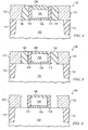
Figure 1 , illustrates afirst embodiment structure 100 of the present invention that is formed in asemiconductor body 102. Thesemiconductor body 102 can be a bulk semiconductor substrate, a region (e.g., well or tub) within a substrate, or a semiconductor layer over a substrate. For example, the present invention works well with semiconductor-on-insulator (SOI) technology. In the preferred embodiment, the semiconductor body is made of silicon. In other embodiments, other materials can be used. - The
structure 100 is formed in an active region of thesemiconductor body 102. The active region is delineated from other active regions byisolation region 112. In the preferred embodiment,isolation region 112 is a trench isolation (e.g., shallow trench isolation or STI) region that surrounds the active area. TheSTI region 112 can be formed, for example, by forming a trench that is filled with a dielectric such as silicon oxide or a silicon nitride. One purpose of theisolation region 112 is to electrically isolatestructures 100 in the active region from surrounding structures. In other embodiments, the isolation could be created by deep trench isolation, mesa isolation, or field isolation, as but three examples. - In the illustrated example, the active region contains a
transistor 100.Transistor 100 includes agate electrode 104 that is disposed over an upper surface of thesemiconductor body 102. Thegate electrode 104 can be formed from one or more conductors such as polysilicon or a metal, or a combination of both. In one embodiment, thegate electrode 104 includes a silicide (e.g., nickel silicide, tungsten silicide, titanium silicide) overlying a polysilicon region. The metal gate can be a metal (e.g., Ir, Ru, RuTa, Ti, Mo), metal silicide (e.g., a fully silicided gate), metal nitride (e.g., HfN, TiN, TaSiN) or other. - The
gate electrode 104 is electrically insulated from achannel region 118 by agate dielectric 106. The gate dielectric can be an oxide, a nitride or a combination of oxide and nitride (e.g., silicon oxynitride (SiON) or an oxide-nitride-oxide (ONO) stack), for example. In other embodiments, thegate dielectric 106 can be a high-k dielectric (i.e., a dielectric with a dielectric constant greater than the dielectric constant of Si3N4). Examples of high-k dielectrics that can be used as a gate dielectric include HfO2, (nitrided) Hf silicate, Al2O3, ZrO2, Zr-Al-O, and Zr silicate. - A
hard mask layer 108 overlies thegate electrode 104. Thehard mask layer 108 is typically formed from an insulating material, such as silicon nitride. This layer is typically formed as part of the fabrication process of the gate electrode and can be eliminated if desired. - A
sidewall spacer 110 is disposed along a sidewall of thegate electrode 104 and, in this example,hard mask layer 108. In one embodiment, thesidewall spacer 110 includes multiple layers such as a nitride and an oxide. In other embodiments, thesidewall spacer 110 can be a single oxide region or a single nitride region. In yet other embodiments, other materials can be used. - The
transistor 100 also includes source/drain regions 114. During operation, current will flow between the source/drain regions 114 depending upon a voltage applied to thegate electrode 104. The present invention applies equally to n-channel transistors (e.g., where the source/drain regions 114 are doped with n-type impurities and thechannel 118 is doped with p-type impurities) and p-channel transistors (e.g., where the source/drain regions 114 are doped with p-type impurities and thechannel 118 is doped with n-type impurities). The invention also applies to both depletion mode and enhancement mode transistors. A silicide region (not shown) can be included over the source/drain regions 114. - In preferred embodiments of the invention, the source/
drain regions 114 each further include a region of asecond semiconductor material 116 embedded within thesemiconductor body 102. Advantageously, thesemiconductor material 116 is a different material than the material ofsemiconductor body 102. For example, by using a material with a different lattice constant astrained channel 118 can be formed. This strained channel will enhance the mobility of carriers during operation thus creating a faster transistor. - In a first embodiment, the
semiconductor body 102 is made from silicon and thesecond semiconductor material 116 is silicon germanium (SiGe). Silicon germanium has a larger natural lattice constant than silicon and will therefore create a compressive channel stress. This situation is ideal for p-channel transistors. In another embodiment, the second semiconductor material is silicon carbon (SiC), which has a natural lattice constant that is smaller than that of silicon. In that case, a tensile channel stress will be created, which speeds up the electron carriers in an n-channel transistor. - In one embodiment, the n-channel transistor and the p-channel transistor of a CMOS implementation are formed using different materials. As a first example, the different conductivity-type transistors can each include an embedded
region 116 with a different material (e.g., SiGe for the p-channel and SiC for the n-channel). In another example, transistors of one type (e.g., p-channel) can include an embedded region 116 (e.g., silicon germanium) while the transistors of the other type (e.g., n-channel) include no embeddedregion 116 at all (i.e., the source/drain regions are only silicon). In yet another example, all transistors (both n-channel and p-channel) are identical. - In the illustrated embodiment, the embedded
semiconductor material 116 extends above the upper surface of thesemiconductor body 102. This feature is not required. Thesemiconductor material 116 can be substantially planar with thesemiconductor body 102 or could be recessed below the upper surface of thesemiconductor body 102. In one embodiment, which is not illustrated, the embeddedmaterial 116 is recessed below the upper surface and covered with a layer of silicon, which can be planar with the remaining silicon body. - Advantageously, the embedded
material 116 extends from thegate stack 104 by a distance that is independent of the length of the source/drain 114. It has been discovered that the length of the embeddedmaterial 116 influences the amount of strain placed onchannel 118. When the length is constant, the strain can be more easily controlled even when the spacing between transistors is not constant. In other words, the stress variations between dense and isolated transistors will be small. As a result, in this preferred embodiment, the region ofsecond semiconductor material 116 is adjacent thesidewall spacer 110 but laterally spaced from theisolation region 112. Since the length of the embeddedmaterial region 116 is constant, the amount by which thematerial 116 is laterally spaced from theisolation region 112 will be a function of the distance between theisolation region 112 and the gate electrode 104 (or sidewall spacer 110). - A first embodiment process to fabricate the transistor of
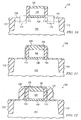
Figure 1 will be described with respect toFigures 2-10 . This process flow describes preferred manufacturing processes and techniques. As will be recognized by one of skill in the art, a number of variations are possible. - Referring first to
Figure 2 , a transistor has been partially fabricated. In particular,STI regions 112 and a gate stack, which includesgate dielectric 106,gate electrode 104, andhard mask layer 108, have been formed using conventional processes.Sidewall spacers 110 have also been formed along sidewalls of thegate electrode 104. These spacers can be formed by conformally depositing an insulating material and anisotropically etching the material. The thickness of the spacer can be determined by the desired dimension of the source/drain extension (or lightly doped source/drain region), which is not explicitly illustrated. - Turning now to
Figure 3 ,sacrificial sidewall spacers 120 are formed adjacent thesidewall spacers 110. Thesespacers 120 can be formed by conformally depositing the spacer material and anisotropically etching the material. The spacer material, which can be either an insulator or a conductor, is selected such that it can be selectively removed with respect to thesidewall spacer 110 andhard mask layer 108. In a preferred embodiment, the sacrificial spacer is formed using low temperature oxide (LTO) process. This thickness of the spacer is determined by the desired length of the embedded semiconductor region (116 inFigure 1 ). - In one exemplary embodiment, the sacrificial spacer has a length of between about 30 nm and 100 nm along the surface of the
semiconductor body 102. As a point of reference, thegate electrode 104 has a length of between about 30 nm and 100 nm. Consequently, the ratio of the sacrificial spacer length to the gate length is between about 1:2 and 2:1. As will become clear below, the length of the sacrificial spacer along the surface of thebody 102 will define the length of the embeddedsemiconductor region 116. - A
planarization layer 122 can then be formed over the structure as shown inFigure 4 . The planarization layer material is selected such thatsacrificial spacer 120 can be removed selectively with respect to thelayer 122. In one embodiment, theplanarization layer 122 is formed by depositing and reflowing a layer of borophosphosilicate glass (BPSG). In other embodiments, other materials can be used. - Referring next to
Figure 5 , an upper surface of the wafer is removed. This process can be performed with a chemical-mechanical polish (CMP) or a reactive ion etch (RIE). In the illustrated embodiment, the resulting structure is planar. In other embodiments (seeFigure 14 , for example), this result is not required. After the process, portions of thesacrificial spacer 120 will be exposed. - As shown in
Figure 6 , thesacrificial spacer 120 is removed selective to thesidewall spacers 110 and theplanarization layer 122. In the preferred embodiment, an isotropic wet etch is performed. In one specific embodiment, thesacrificial spacer 120 is made from a low temperature oxide, the sidewall spacer 110 (or at least the exposed portions of the sidewall spacer 110) is made from a nitride, and the planarization layer is made from BPSG. With these materials, the sacrificial oxide can be removed. - Referring next to
Figure 7 , recesses 124 are etched into regions of thesemiconductor body 102 that are exposed by the removal of the sacrificial spacer. In various embodiments, the recess can be etched to a depth between about 20 nm and about 150 nm. As but two examples, a recess of a depth of about 30 nm to about 45 nm can be used in an SOI embodiment and a recess of about 100 nm can be etched for a bulk embodiment. The length of the recess will correspond to the length of thesacrificial spacer 120 and the width of the recess (i.e., the distance into and out of the page inFigure 7 ) will correspond to the transistor width (or active area width). - The embedded
semiconductor regions 116 can then be formed as illustrated inFigure 8 . In one embodiment, SiGe or SiC is selectively deposited using an epitaxial growth process. This semiconductor can be doped in situ or deposited undoped. In one example, silicon germanium is doped in situ with boron to create a p-channel transistor. If the n-channel transistors are to include regions embedded with a different material, they can be masked (e.g., with photoresist) at this point. If the n-channel transistors include no embedded region, they would be masked during the step of forming the recess as well. In another example, silicon carbon is deposited and doped in situ with arsenic or phosphorus. - As shown in
Figure 9 , theplanarization layer 122 can then be removed This leads to the basic structure as discussed above with respect toFigure 1 . As an optional step, source/drain dopants 126 can be implanted, as shown inFigure 10 . For p-channel transistors, the source/drain dopants 126 can be boron and for n-channel transistors, the source/drain dopants 126 can be arsenic or phosphorus, for example. - An alternate process for fabricating a transistor is illustrated with respect to
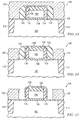
Figures 11-16 . Due to the similarity in the two processes, many of the details will not be repeated. It is understood that either process can be varied using any of the details discussed herein. -
Figure 11 illustrates a structure that is similar to the structure ofFigure 2 but additionally includes amasking layer 128. Maskinglayer 128 can be included to protect the gate stack andsidewall spacers 110 during the removal of thesacrificial sidewall spacer 120. In one example, themasking layer 128 is a silicon nitride (e.g., Si3N4) with a thickness of about 10 to about 50 nm. By including thisliner 128, thesidewall spacer 110 and thesacrificial spacer 120 can be formed from the same material. - The formation of the
sacrificial spacer 120 is shown inFigure 12 and the formation ofplanarization layer 122 is shown inFigure 13 . As before, it is desired that the materials ofsacrificial spacer 120 andplanarization layer 122 be selected so that thespacer 120 can be selectively removed. In one embodiment, theplanarization layer 122 is formed from a resist while the sacrificial spacer is formed from an oxide. As an example, the resist material can be spun on in a substantially planar manner. As noted above, the choice of sacrificial spacer material is independent of the material ofsidewall spacer 110. - The planarization material is then etched back as shown in
Figure 14 . The amount of etch back should be sufficient to expose a portion of thesacrificial spacer 120 but still leaveenough material 122 to protectsemiconductor body 102 during the subsequent recess etch. As an example, the thickness of the resist layer can be 500-1000 nm before the recess, and 50-100nm after the recess. - The sacrificial spacer can then be selectively removed as shown in
Figure 15 . This removal can be done by wet etch using diluted or buffered HF in the case of an oxide sacrificial spacer, or alternatively by dry etching. This step will expose a portion of themasking layer 128 over thesemiconductor body 102. This exposed portion of the masking layer can then be opened, for example, using an anisotropic etch process. -
Figure 16 illustrates the recess etch that was described earlier with respect toFigure 7 . In a next step, the resist 122 is removed as shown inFigure 17 and the trenches are filled as described in the earlier embodiment. The selective deposition ofsemiconductor material 116 is illustrated inFigure 18 , where thelayer 128 is used as a mask for the selective deposition. Thelayer 128 can then be removed or allowed to remain. - Additional processes such as interlevel dielectrics, contact plugs and metallization are not shown, but would be included.
-
Figures 19 and 20 illustrate two embodiments that can utilize concepts of the present invention. InFigure 19 , twotransistors same semiconductor body 102 but have different dimensions. Shallowtrench isolation regions 112 are shown but it is understood that other isolation techniques (e.g., mesa isolation for SOI devices) could be utilized. It is also understood that these two transistors are shown next to each to simplify illustration. The transistors could be spaced from one another anywhere on the die and could have source/drain current paths that are oriented at different angles from each other. - One point of interest in the structure of
Figure 19 is that bothtransistors semiconductor regions 116 of the same length (i.e., the distance extending in parallel with the current path). The width of the embedded regions would be the same as the transistor's channel width and may vary from transistor to transistor. As shown inFigure 19 , theregion 116a has a length L that is the same as the length L of theregion 116b. This is true even though the distance between sidewall spacer 110a andisolation region 112 is smaller than the distance betweensidewall spacer 110b andisolation region 112. Since the embeddedregions -
Figure 20 illustrates another embodiment where twotransistors region 116a-r is spaced from the embeddedregion 116b-1 without any intervening isolation regions. This situation can occur, for example, when two transistors have a shared source/drain region. Despite the shared source/drain, eachtransistor regions 116 of the same length. - The embedded
regions transistor 100a is an n-channel transistor andtransistor 100b is a p-channel transistor, theregion 116a can be embedded with SiC while theregion 116 is embedded with SiGe. A silicide region or other conductor (not shown) can be used to electrically couple across the common source/drain region. - While this invention has been described with reference to illustrative embodiments, this description is not intended to be construed in a limiting sense. Various modifications and combinations of the illustrative embodiments, as well as other embodiments of the invention, will be apparent to persons skilled in the art upon reference to the description. It is therefore intended that the appended claims encompass any such modifications or embodiments.
Claims (6)
- A semiconductor device comprising:a semiconductor body formed from a first semiconductor material;a first gate electrode disposed over an upper surface of the semiconductor body;a first sidewall spacer disposed along a sidewall of the first gate electrode;a second gate electrode disposed over an upper surface of the semiconductor body;a second sidewall spacer disposed along a sidewall of the second gate electrode;a first region of a second semiconductor material embedded within the semiconductor body adjacent the first sidewall spacer; anda second region of the second semiconductor material embedded within the semiconductor body adjacent the second sidewall spacer, the second region laterally spaced from the first region without any intervening isolation material.
- The device of claim 1, further comprising:a third sidewall spacer disposed along a second sidewall of the first gate electrode, the second sidewall opposed from the first sidewall;a fourth sidewall spacer disposed along a second sidewall of the second gate electrode, the second sidewall opposed from the first sidewall;a third region of the second semiconductor material embedded within the semiconductor body adj acent the third sidewall spacer; anda fourth region of the second semiconductor material embedded within the semiconductor body adjacent the fourth sidewall spacer.
- The device of claim 2, further comprising a trench isolation structure surrounding the first and second gate electrodes and the first, second, third and fourth regions of the second semiconductor material.
- The device of claim 3, wherein the trench isolation structure is laterally spaced from each of the first, second, third and fourth regions of the second semiconductor material in the direction of a current path beneath the first and second gate electrodes.
- The device of claim 1, wherein the first semiconductor material comprises silicon and the second semiconductor material comprises silicon germanium.
- The device of claim 1, wherein the first semiconductor material comprises silicon and the second semiconductor material comprises silicon carbon.
Applications Claiming Priority (3)
| Application Number | Priority Date | Filing Date | Title |
|---|---|---|---|
| US11/224,825 US8003470B2 (en) | 2005-09-13 | 2005-09-13 | Strained semiconductor device and method of making the same |
| EP20060120572 EP1763073B1 (en) | 2005-09-13 | 2006-09-13 | Strained Semiconductor Device |
| EP20100153752 EP2180504B1 (en) | 2005-09-13 | 2006-09-13 | Method of fabricating a semiconductor device |
Related Parent Applications (3)
| Application Number | Title | Priority Date | Filing Date |
|---|---|---|---|
| EP20060120572 Division EP1763073B1 (en) | 2005-09-13 | 2006-09-13 | Strained Semiconductor Device |
| EP20100153752 Division-Into EP2180504B1 (en) | 2005-09-13 | 2006-09-13 | Method of fabricating a semiconductor device |
| EP20100153752 Division EP2180504B1 (en) | 2005-09-13 | 2006-09-13 | Method of fabricating a semiconductor device |
Publications (3)
| Publication Number | Publication Date |
|---|---|
| EP2720256A2 true EP2720256A2 (en) | 2014-04-16 |
| EP2720256A3 EP2720256A3 (en) | 2014-06-04 |
| EP2720256B1 EP2720256B1 (en) | 2016-05-25 |
Family
ID=37487523
Family Applications (3)
| Application Number | Title | Priority Date | Filing Date |
|---|---|---|---|
| EP20060120572 Expired - Fee Related EP1763073B1 (en) | 2005-09-13 | 2006-09-13 | Strained Semiconductor Device |
| EP14150531.3A Not-in-force EP2720256B1 (en) | 2005-09-13 | 2006-09-13 | Strained semiconductor device |
| EP20100153752 Expired - Fee Related EP2180504B1 (en) | 2005-09-13 | 2006-09-13 | Method of fabricating a semiconductor device |
Family Applications Before (1)
| Application Number | Title | Priority Date | Filing Date |
|---|---|---|---|
| EP20060120572 Expired - Fee Related EP1763073B1 (en) | 2005-09-13 | 2006-09-13 | Strained Semiconductor Device |
Family Applications After (1)
| Application Number | Title | Priority Date | Filing Date |
|---|---|---|---|
| EP20100153752 Expired - Fee Related EP2180504B1 (en) | 2005-09-13 | 2006-09-13 | Method of fabricating a semiconductor device |
Country Status (4)
| Country | Link |
|---|---|
| US (4) | US8003470B2 (en) |
| EP (3) | EP1763073B1 (en) |
| JP (1) | JP4644173B2 (en) |
| CN (1) | CN1945854B (en) |
Families Citing this family (47)
| Publication number | Priority date | Publication date | Assignee | Title |
|---|---|---|---|---|
| US7553732B1 (en) * | 2005-06-13 | 2009-06-30 | Advanced Micro Devices, Inc. | Integration scheme for constrained SEG growth on poly during raised S/D processing |
| US20060281271A1 (en) * | 2005-06-13 | 2006-12-14 | Advanced Micro Devices, Inc. | Method of forming a semiconductor device having an epitaxial layer and device thereof |
| US7572705B1 (en) | 2005-09-21 | 2009-08-11 | Advanced Micro Devices, Inc. | Semiconductor device and method of manufacturing a semiconductor device |
| US7696019B2 (en) * | 2006-03-09 | 2010-04-13 | Infineon Technologies Ag | Semiconductor devices and methods of manufacturing thereof |
| JP2007243105A (en) * | 2006-03-13 | 2007-09-20 | Sony Corp | Semiconductor device and method for manufacturing the same |
| DE102006015075A1 (en) * | 2006-03-31 | 2007-10-11 | Advanced Micro Devices, Inc., Sunnyvale | Technique for providing voltage sources in MOS transistors in close proximity to a channel region |
| US7763517B2 (en) * | 2007-02-12 | 2010-07-27 | Macronix International Co., Ltd. | Method of forming non-volatile memory cell |
| JP5286701B2 (en) | 2007-06-27 | 2013-09-11 | ソニー株式会社 | Semiconductor device and manufacturing method of semiconductor device |
| US9640666B2 (en) * | 2007-07-23 | 2017-05-02 | GlobalFoundries, Inc. | Integrated circuit employing variable thickness film |
| US7652336B2 (en) | 2007-08-06 | 2010-01-26 | International Business Machines Corporation | Semiconductor devices and methods of manufacture thereof |
| JP5389346B2 (en) * | 2007-10-11 | 2014-01-15 | 富士通セミコンダクター株式会社 | MOS field effect transistor and manufacturing method thereof |
| US7923365B2 (en) * | 2007-10-17 | 2011-04-12 | Samsung Electronics Co., Ltd. | Methods of forming field effect transistors having stress-inducing sidewall insulating spacers thereon |
| JP5107680B2 (en) * | 2007-11-16 | 2012-12-26 | パナソニック株式会社 | Semiconductor device |
| US7786518B2 (en) * | 2007-12-27 | 2010-08-31 | Texas Instruments Incorporated | Growth of unfaceted SiGe in MOS transistor fabrication |
| US8293631B2 (en) | 2008-03-13 | 2012-10-23 | International Business Machines Corporation | Semiconductor devices having tensile and/or compressive stress and methods of manufacturing |
| US7892932B2 (en) | 2008-03-25 | 2011-02-22 | International Business Machines Corporation | Semiconductor devices having tensile and/or compressive strain and methods of manufacturing and design structure |
| US7772095B2 (en) * | 2008-05-28 | 2010-08-10 | International Business Machines Corporation | Integrated circuit having localized embedded SiGe and method of manufacturing |
| KR101399099B1 (en) * | 2008-06-02 | 2014-05-26 | 삼성전자주식회사 | Semiconductor devices including a contact structure and methods of forming the same |
| KR101035614B1 (en) * | 2008-10-23 | 2011-05-19 | 주식회사 동부하이텍 | Method Manufactruing of Flash Memory Device |
| US8106456B2 (en) * | 2009-07-29 | 2012-01-31 | International Business Machines Corporation | SOI transistors having an embedded extension region to improve extension resistance and channel strain characteristics |
| JP5434360B2 (en) | 2009-08-20 | 2014-03-05 | ソニー株式会社 | Semiconductor device and manufacturing method thereof |
| US20110049582A1 (en) * | 2009-09-03 | 2011-03-03 | International Business Machines Corporation | Asymmetric source and drain stressor regions |
| KR101674179B1 (en) * | 2010-04-06 | 2016-11-10 | 삼성전자주식회사 | Semiconductor dievices having a field effect transistor and methods of forming the same |
| CN102214574B (en) * | 2010-04-07 | 2013-06-12 | 中国科学院微电子研究所 | Method for manufacturing semiconductor device |
| CN102314927B (en) * | 2010-07-06 | 2014-02-05 | 中国科学院物理研究所 | Magnetic random access memory cell array, memory and reading/writing method thereof |
| US8361859B2 (en) * | 2010-11-09 | 2013-01-29 | International Business Machines Corporation | Stressed transistor with improved metastability |
| US8941182B2 (en) * | 2011-06-07 | 2015-01-27 | Globalfoundries Inc. | Buried sublevel metallizations for improved transistor density |
| US8697557B2 (en) * | 2011-06-07 | 2014-04-15 | Globalfoundries Inc. | Method of removing gate cap materials while protecting active area |
| US8921944B2 (en) * | 2011-07-19 | 2014-12-30 | United Microelectronics Corp. | Semiconductor device |
| CN102903638B (en) * | 2011-07-29 | 2016-03-30 | 中国科学院微电子研究所 | Semiconductor device and manufacture method thereof |
| FR2985089B1 (en) * | 2011-12-27 | 2015-12-04 | Commissariat Energie Atomique | TRANSISTOR AND METHOD FOR MANUFACTURING A TRANSISTOR |
| US8841190B2 (en) | 2012-03-30 | 2014-09-23 | The Institute of Microelectronics Chinese Academy of Science | MOS device for making the source/drain region closer to the channel region and method of manufacturing the same |
| CN103367151B (en) * | 2012-03-30 | 2015-12-16 | 中国科学院微电子研究所 | Make source/drain region closer to MOS device of channel region and preparation method thereof |
| US8866230B2 (en) * | 2012-04-26 | 2014-10-21 | United Microelectronics Corp. | Semiconductor devices |
| CN103632973B (en) | 2012-08-23 | 2017-01-25 | 中国科学院微电子研究所 | Semiconductor device and manufacture method thereof |
| US9419126B2 (en) * | 2013-03-15 | 2016-08-16 | GlobalFoundries, Inc. | Integrated circuits and methods for fabricating integrated circuits with active area protection |
| CN104103586B (en) * | 2013-04-10 | 2017-03-22 | 中芯国际集成电路制造(上海)有限公司 | Method for forming semiconductor device |
| CN104143512B (en) * | 2013-05-09 | 2017-02-22 | 中芯国际集成电路制造(上海)有限公司 | Method for manufacturing PMOS transistor |
| CN104517822B (en) * | 2013-09-27 | 2017-06-16 | 中芯国际集成电路制造(北京)有限公司 | A kind of manufacture method of semiconductor devices |
| US9379214B2 (en) * | 2014-02-14 | 2016-06-28 | Semi Solutions Llc | Reduced variation MOSFET using a drain-extension-last process |
| EP3116384B1 (en) | 2014-03-10 | 2019-10-02 | Innerspace Neuro Solutions, Inc. | Air line protection coupling for a catheter |
| US9941388B2 (en) * | 2014-06-19 | 2018-04-10 | Globalfoundries Inc. | Method and structure for protecting gates during epitaxial growth |
| TWI555120B (en) * | 2014-10-14 | 2016-10-21 | 力晶科技股份有限公司 | Semiconductor device and method for fabricating the same |
| US10008582B2 (en) * | 2016-11-28 | 2018-06-26 | Globalfoundries Inc. | Spacers for tight gate pitches in field effect transistors |
| CN109473429B (en) * | 2018-10-26 | 2021-08-03 | 中国科学院微电子研究所 | Semiconductor device, method of manufacturing the same, and electronic apparatus including the same |
| US11289375B2 (en) | 2020-03-23 | 2022-03-29 | International Business Machines Corporation | Fully aligned interconnects with selective area deposition |
| CN116799005B (en) * | 2023-08-22 | 2023-11-28 | 合肥晶合集成电路股份有限公司 | Semiconductor structure and preparation method thereof |
Citations (2)
| Publication number | Priority date | Publication date | Assignee | Title |
|---|---|---|---|---|
| US20040173815A1 (en) | 2003-03-04 | 2004-09-09 | Yee-Chia Yeo | Strained-channel transistor structure with lattice-mismatched zone |
| US20050101077A1 (en) | 2003-01-17 | 2005-05-12 | Sharp Laboratories Of America, Inc. | Sacrificial shallow trench isolation oxide liner for strained-silicon channel CMOS devices |
Family Cites Families (49)
| Publication number | Priority date | Publication date | Assignee | Title |
|---|---|---|---|---|
| JPH03272182A (en) | 1990-03-22 | 1991-12-03 | Matsushita Electron Corp | Manufacture of semiconductor device |
| JPH0479337A (en) | 1990-07-23 | 1992-03-12 | Oki Electric Ind Co Ltd | Semiconductor element and its production |
| US5364497A (en) * | 1993-08-04 | 1994-11-15 | Analog Devices, Inc. | Method for fabricating microstructures using temporary bridges |
| US5679610A (en) * | 1994-12-15 | 1997-10-21 | Kabushiki Kaisha Toshiba | Method of planarizing a semiconductor workpiece surface |
| DE19720008A1 (en) | 1997-05-13 | 1998-11-19 | Siemens Ag | Integrated CMOS circuit arrangement and method for its production |
| US6214675B1 (en) * | 1999-02-08 | 2001-04-10 | Lucent Technologies Inc. | Method for fabricating a merged integrated circuit device |
| US6136679A (en) * | 1999-03-05 | 2000-10-24 | Taiwan Semiconductor Manufacturing Company | Gate micro-patterning process |
| US6294817B1 (en) * | 1999-12-13 | 2001-09-25 | Infineon Technologies Ag | Source/drain-on insulator (S/DOI) field effect transistor using oxidized amorphous silicon and method of fabrication |
| US6448180B2 (en) * | 2000-03-09 | 2002-09-10 | Advanced Micro Devices, Inc. | Deposition of in-situ doped semiconductor film and undoped semiconductor film in the same reaction chamber |
| US6403482B1 (en) * | 2000-06-28 | 2002-06-11 | International Business Machines Corporation | Self-aligned junction isolation |
| KR20020007848A (en) * | 2000-07-19 | 2002-01-29 | 박종섭 | Semiconductor Device and Method for Fabricating the Same |
| JP3872639B2 (en) | 2000-08-31 | 2007-01-24 | 株式会社村上開明堂 | Electric retractable door mirror |
| US6495437B1 (en) * | 2001-02-09 | 2002-12-17 | Advanced Micro Devices, Inc. | Low temperature process to locally form high-k gate dielectrics |
| US6489206B2 (en) | 2001-03-22 | 2002-12-03 | United Microelectronics Corp. | Method for forming self-aligned local-halo metal-oxide-semiconductor device |
| JP2004538650A (en) * | 2001-08-10 | 2004-12-24 | スピネカ セミコンダクター, インコーポレイテッド | Transistor having high dielectric constant gate insulating layer, source and drain forming Schottky contact with substrate |
| US6417056B1 (en) * | 2001-10-18 | 2002-07-09 | Chartered Semiconductor Manufacturing Ltd. | Method to form low-overlap-capacitance transistors by forming microtrench at the gate edge |
| US6621131B2 (en) * | 2001-11-01 | 2003-09-16 | Intel Corporation | Semiconductor transistor having a stressed channel |
| US7226504B2 (en) | 2002-01-31 | 2007-06-05 | Sharp Laboratories Of America, Inc. | Method to form thick relaxed SiGe layer with trench structure |
| US6583000B1 (en) | 2002-02-07 | 2003-06-24 | Sharp Laboratories Of America, Inc. | Process integration of Si1-xGex CMOS with Si1-xGex relaxation after STI formation |
| US7138310B2 (en) | 2002-06-07 | 2006-11-21 | Amberwave Systems Corporation | Semiconductor devices having strained dual channel layers |
| US6812103B2 (en) | 2002-06-20 | 2004-11-02 | Micron Technology, Inc. | Methods of fabricating a dielectric plug in MOSFETS to suppress short-channel effects |
| US6787464B1 (en) * | 2002-07-02 | 2004-09-07 | Advanced Micro Devices, Inc. | Method of forming silicide layers over a plurality of semiconductor devices |
| US7473947B2 (en) | 2002-07-12 | 2009-01-06 | Intel Corporation | Process for ultra-thin body SOI devices that incorporate EPI silicon tips and article made thereby |
| KR100437856B1 (en) * | 2002-08-05 | 2004-06-30 | 삼성전자주식회사 | MOS Transister and Method of manufacturing semiconductor device comprising the same |
| US7279367B1 (en) * | 2004-12-07 | 2007-10-09 | T-Ram Semiconductor, Inc. | Method of manufacturing a thyristor semiconductor device |
| US6703648B1 (en) | 2002-10-29 | 2004-03-09 | Advanced Micro Devices, Inc. | Strained silicon PMOS having silicon germanium source/drain extensions and method for its fabrication |
| JP2004153173A (en) | 2002-10-31 | 2004-05-27 | Sharp Corp | Method for manufacturing semiconductor device |
| US7090967B2 (en) * | 2002-12-30 | 2006-08-15 | Infineon Technologies Ag | Pattern transfer in device fabrication |
| JP4477886B2 (en) * | 2003-04-28 | 2010-06-09 | 株式会社ルネサステクノロジ | Manufacturing method of semiconductor device |
| US7129539B2 (en) * | 2003-05-15 | 2006-10-31 | Sharp Kabushiki Kaisha | Semiconductor storage device and manufacturing method therefor, semiconductor device, portable electronic equipment and IC card |
| US20040262683A1 (en) * | 2003-06-27 | 2004-12-30 | Bohr Mark T. | PMOS transistor strain optimization with raised junction regions |
| US7078742B2 (en) | 2003-07-25 | 2006-07-18 | Taiwan Semiconductor Manufacturing Co., Ltd. | Strained-channel semiconductor structure and method of fabricating the same |
| US6891192B2 (en) | 2003-08-04 | 2005-05-10 | International Business Machines Corporation | Structure and method of making strained semiconductor CMOS transistors having lattice-mismatched semiconductor regions underlying source and drain regions |
| US7101742B2 (en) | 2003-08-12 | 2006-09-05 | Taiwan Semiconductor Manufacturing Company, Ltd. | Strained channel complementary field-effect transistors and methods of manufacture |
| US20050035369A1 (en) | 2003-08-15 | 2005-02-17 | Chun-Chieh Lin | Structure and method of forming integrated circuits utilizing strained channel transistors |
| DE10339989B4 (en) * | 2003-08-29 | 2008-04-17 | Advanced Micro Devices, Inc., Sunnyvale | A method of making a conformal spacer adjacent to a gate electrode structure |
| US7138320B2 (en) * | 2003-10-31 | 2006-11-21 | Advanced Micro Devices, Inc. | Advanced technique for forming a transistor having raised drain and source regions |
| US8097924B2 (en) | 2003-10-31 | 2012-01-17 | Taiwan Semiconductor Manufacturing Company, Ltd. | Ultra-shallow junction MOSFET having a high-k gate dielectric and in-situ doped selective epitaxy source/drain extensions and a method of making same |
| KR100583105B1 (en) * | 2003-12-24 | 2006-05-23 | 주식회사 하이닉스반도체 | Method for Detecting End-Point of Chemical Mechanical Polishing |
| US7023059B1 (en) * | 2004-03-01 | 2006-04-04 | Advanced Micro Devices, Inc. | Trenches to reduce lateral silicide growth in integrated circuit technology |
| US7205206B2 (en) * | 2004-03-03 | 2007-04-17 | International Business Machines Corporation | Method of fabricating mobility enhanced CMOS devices |
| US7195963B2 (en) * | 2004-05-21 | 2007-03-27 | Freescale Semiconductor, Inc. | Method for making a semiconductor structure using silicon germanium |
| US7172933B2 (en) * | 2004-06-10 | 2007-02-06 | Taiwan Semiconductor Manufacturing Company, Ltd. | Recessed polysilicon gate structure for a strained silicon MOSFET device |
| US7361563B2 (en) * | 2004-06-17 | 2008-04-22 | Samsung Electronics Co., Ltd. | Methods of fabricating a semiconductor device using a selective epitaxial growth technique |
| US7227205B2 (en) | 2004-06-24 | 2007-06-05 | International Business Machines Corporation | Strained-silicon CMOS device and method |
| US7413957B2 (en) * | 2004-06-24 | 2008-08-19 | Applied Materials, Inc. | Methods for forming a transistor |
| US7135724B2 (en) * | 2004-09-29 | 2006-11-14 | International Business Machines Corporation | Structure and method for making strained channel field effect transistor using sacrificial spacer |
| KR100612420B1 (en) | 2004-10-20 | 2006-08-16 | 삼성전자주식회사 | Semiconductor device and method for forming the same |
| CN100463143C (en) * | 2005-07-07 | 2009-02-18 | 中芯国际集成电路制造(上海)有限公司 | Strain source-drain CMOS integrating method with oxide separation layer |
-
2005
- 2005-09-13 US US11/224,825 patent/US8003470B2/en not_active Expired - Fee Related
-
2006
- 2006-09-13 JP JP2006247813A patent/JP4644173B2/en not_active Expired - Fee Related
- 2006-09-13 CN CN200610143172XA patent/CN1945854B/en not_active Expired - Fee Related
- 2006-09-13 EP EP20060120572 patent/EP1763073B1/en not_active Expired - Fee Related
- 2006-09-13 EP EP14150531.3A patent/EP2720256B1/en not_active Not-in-force
- 2006-09-13 EP EP20100153752 patent/EP2180504B1/en not_active Expired - Fee Related
-
2011
- 2011-07-29 US US13/193,692 patent/US8624334B2/en active Active
-
2013
- 2013-11-22 US US14/087,918 patent/US8946034B2/en not_active Expired - Fee Related
-
2015
- 2015-01-13 US US14/595,977 patent/US9559204B2/en active Active
Patent Citations (2)
| Publication number | Priority date | Publication date | Assignee | Title |
|---|---|---|---|---|
| US20050101077A1 (en) | 2003-01-17 | 2005-05-12 | Sharp Laboratories Of America, Inc. | Sacrificial shallow trench isolation oxide liner for strained-silicon channel CMOS devices |
| US20040173815A1 (en) | 2003-03-04 | 2004-09-09 | Yee-Chia Yeo | Strained-channel transistor structure with lattice-mismatched zone |
Also Published As
| Publication number | Publication date |
|---|---|
| US20140077299A1 (en) | 2014-03-20 |
| EP2180504B1 (en) | 2015-03-25 |
| US8003470B2 (en) | 2011-08-23 |
| EP2180504A2 (en) | 2010-04-28 |
| CN1945854B (en) | 2012-01-11 |
| EP2720256B1 (en) | 2016-05-25 |
| US20110278680A1 (en) | 2011-11-17 |
| US8946034B2 (en) | 2015-02-03 |
| US20150123201A1 (en) | 2015-05-07 |
| CN1945854A (en) | 2007-04-11 |
| EP2180504A3 (en) | 2013-03-13 |
| EP1763073A2 (en) | 2007-03-14 |
| US20070057324A1 (en) | 2007-03-15 |
| EP1763073B1 (en) | 2013-06-19 |
| JP4644173B2 (en) | 2011-03-02 |
| EP1763073A3 (en) | 2009-08-26 |
| JP2007110098A (en) | 2007-04-26 |
| US8624334B2 (en) | 2014-01-07 |
| US9559204B2 (en) | 2017-01-31 |
| EP2720256A3 (en) | 2014-06-04 |
Similar Documents
| Publication | Publication Date | Title |
|---|---|---|
| US9559204B2 (en) | Strained semiconductor device and method of making the same | |
| TWI446453B (en) | Stressed field effect transistor and methods for its fabrication | |
| KR101023208B1 (en) | Mosfet device with tensile strained substrate and method of making the same | |
| JP5220348B2 (en) | Semiconductor structure and type and method thereof (structure and method for forming a multi-layer buried stressor) | |
| KR100968182B1 (en) | High-mobility bulk silicon pfet | |
| KR100998300B1 (en) | Virtual body-contacted trigate | |
| US7928474B2 (en) | Forming embedded dielectric layers adjacent to sidewalls of shallow trench isolation regions | |
| US7026232B1 (en) | Systems and methods for low leakage strained-channel transistor | |
| US9373548B2 (en) | CMOS circuit having a tensile stress layer overlying an NMOS transistor and overlapping a portion of compressive stress layer | |
| US7790548B2 (en) | Methods of fabricating field effect transistors including recessed forked gate structures | |
| US7514309B2 (en) | Methods to selectively protect NMOS regions, PMOS regions, and gate layers during EPI process | |
| US7670914B2 (en) | Methods for fabricating multiple finger transistors | |
| US7566609B2 (en) | Method of manufacturing a semiconductor structure | |
| US20060131657A1 (en) | Semiconductor integrated circuit device and method for the same | |
| US9564488B2 (en) | Strained isolation regions | |
| US10199392B2 (en) | FinFET device having a partially dielectric isolated fin structure | |
| US7279406B2 (en) | Tailoring channel strain profile by recessed material composition control | |
| US20230387246A1 (en) | Methods of forming gate structures with uniform gate length | |
| CN103094217B (en) | Manufacture method of transistor | |
| US20240113164A1 (en) | Film modification for gate cut process |
Legal Events
| Date | Code | Title | Description |
|---|---|---|---|
| PUAI | Public reference made under article 153(3) epc to a published international application that has entered the european phase |
Free format text: ORIGINAL CODE: 0009012 |
|
| AC | Divisional application: reference to earlier application |
Ref document number: 1763073 Country of ref document: EP Kind code of ref document: P Ref document number: 2180504 Country of ref document: EP Kind code of ref document: P |
|
| AK | Designated contracting states |
Kind code of ref document: A2 Designated state(s): DE |
|
| PUAL | Search report despatched |
Free format text: ORIGINAL CODE: 0009013 |
|
| AK | Designated contracting states |
Kind code of ref document: A3 Designated state(s): DE |
|
| RIC1 | Information provided on ipc code assigned before grant |
Ipc: H01L 21/336 20060101AFI20140425BHEP Ipc: H01L 29/78 20060101ALI20140425BHEP Ipc: H01L 21/8234 20060101ALI20140425BHEP Ipc: H01L 29/66 20060101ALI20140425BHEP |
|
| 17P | Request for examination filed |
Effective date: 20141201 |
|
| RBV | Designated contracting states (corrected) |
Designated state(s): DE |
|
| RBV | Designated contracting states (corrected) |
Designated state(s): AT BE BG CH CY CZ DE DK EE ES FI FR GB GR HU IE IS IT LI LT LU LV MC NL PL PT RO SE SI SK TR |
|
| 17Q | First examination report despatched |
Effective date: 20150413 |
|
| GRAP | Despatch of communication of intention to grant a patent |
Free format text: ORIGINAL CODE: EPIDOSNIGR1 |
|
| RIC1 | Information provided on ipc code assigned before grant |
Ipc: H01L 21/8234 20060101ALI20160112BHEP Ipc: H01L 29/78 20060101ALI20160112BHEP Ipc: H01L 21/336 20060101AFI20160112BHEP Ipc: H01L 27/088 20060101ALI20160112BHEP Ipc: H01L 29/66 20060101ALI20160112BHEP |
|
| INTG | Intention to grant announced |
Effective date: 20160204 |
|
| GRAS | Grant fee paid |
Free format text: ORIGINAL CODE: EPIDOSNIGR3 |
|
| GRAA | (expected) grant |
Free format text: ORIGINAL CODE: 0009210 |
|
| AC | Divisional application: reference to earlier application |
Ref document number: 1763073 Country of ref document: EP Kind code of ref document: P Ref document number: 2180504 Country of ref document: EP Kind code of ref document: P |
|
| AK | Designated contracting states |
Kind code of ref document: B1 Designated state(s): AT BE BG CH CY CZ DE DK EE ES FI FR GB GR HU IE IS IT LI LT LU LV MC NL PL PT RO SE SI SK TR |
|
| REG | Reference to a national code |
Ref country code: GB Ref legal event code: FG4D |
|
| REG | Reference to a national code |
Ref country code: CH Ref legal event code: EP |
|
| REG | Reference to a national code |
Ref country code: IE Ref legal event code: FG4D Ref country code: AT Ref legal event code: REF Ref document number: 802954 Country of ref document: AT Kind code of ref document: T Effective date: 20160615 |
|
| REG | Reference to a national code |
Ref country code: DE Ref legal event code: R096 Ref document number: 602006049225 Country of ref document: DE |
|
| REG | Reference to a national code |
Ref country code: FR Ref legal event code: PLFP Year of fee payment: 11 |
|
| REG | Reference to a national code |
Ref country code: LT Ref legal event code: MG4D |
|
| REG | Reference to a national code |
Ref country code: NL Ref legal event code: MP Effective date: 20160525 |
|
| PG25 | Lapsed in a contracting state [announced via postgrant information from national office to epo] |
Ref country code: NL Free format text: LAPSE BECAUSE OF FAILURE TO SUBMIT A TRANSLATION OF THE DESCRIPTION OR TO PAY THE FEE WITHIN THE PRESCRIBED TIME-LIMIT Effective date: 20160525 Ref country code: FI Free format text: LAPSE BECAUSE OF FAILURE TO SUBMIT A TRANSLATION OF THE DESCRIPTION OR TO PAY THE FEE WITHIN THE PRESCRIBED TIME-LIMIT Effective date: 20160525 Ref country code: LT Free format text: LAPSE BECAUSE OF FAILURE TO SUBMIT A TRANSLATION OF THE DESCRIPTION OR TO PAY THE FEE WITHIN THE PRESCRIBED TIME-LIMIT Effective date: 20160525 |
|
| REG | Reference to a national code |
Ref country code: AT Ref legal event code: MK05 Ref document number: 802954 Country of ref document: AT Kind code of ref document: T Effective date: 20160525 |
|
| PG25 | Lapsed in a contracting state [announced via postgrant information from national office to epo] |
Ref country code: SE Free format text: LAPSE BECAUSE OF FAILURE TO SUBMIT A TRANSLATION OF THE DESCRIPTION OR TO PAY THE FEE WITHIN THE PRESCRIBED TIME-LIMIT Effective date: 20160525 Ref country code: LV Free format text: LAPSE BECAUSE OF FAILURE TO SUBMIT A TRANSLATION OF THE DESCRIPTION OR TO PAY THE FEE WITHIN THE PRESCRIBED TIME-LIMIT Effective date: 20160525 Ref country code: GR Free format text: LAPSE BECAUSE OF FAILURE TO SUBMIT A TRANSLATION OF THE DESCRIPTION OR TO PAY THE FEE WITHIN THE PRESCRIBED TIME-LIMIT Effective date: 20160826 |
|
| PG25 | Lapsed in a contracting state [announced via postgrant information from national office to epo] |
Ref country code: SK Free format text: LAPSE BECAUSE OF FAILURE TO SUBMIT A TRANSLATION OF THE DESCRIPTION OR TO PAY THE FEE WITHIN THE PRESCRIBED TIME-LIMIT Effective date: 20160525 Ref country code: EE Free format text: LAPSE BECAUSE OF FAILURE TO SUBMIT A TRANSLATION OF THE DESCRIPTION OR TO PAY THE FEE WITHIN THE PRESCRIBED TIME-LIMIT Effective date: 20160525 Ref country code: DK Free format text: LAPSE BECAUSE OF FAILURE TO SUBMIT A TRANSLATION OF THE DESCRIPTION OR TO PAY THE FEE WITHIN THE PRESCRIBED TIME-LIMIT Effective date: 20160525 Ref country code: CZ Free format text: LAPSE BECAUSE OF FAILURE TO SUBMIT A TRANSLATION OF THE DESCRIPTION OR TO PAY THE FEE WITHIN THE PRESCRIBED TIME-LIMIT Effective date: 20160525 |
|
| PG25 | Lapsed in a contracting state [announced via postgrant information from national office to epo] |
Ref country code: PL Free format text: LAPSE BECAUSE OF FAILURE TO SUBMIT A TRANSLATION OF THE DESCRIPTION OR TO PAY THE FEE WITHIN THE PRESCRIBED TIME-LIMIT Effective date: 20160525 Ref country code: AT Free format text: LAPSE BECAUSE OF FAILURE TO SUBMIT A TRANSLATION OF THE DESCRIPTION OR TO PAY THE FEE WITHIN THE PRESCRIBED TIME-LIMIT Effective date: 20160525 Ref country code: BE Free format text: LAPSE BECAUSE OF NON-PAYMENT OF DUE FEES Effective date: 20160525 |
|
| REG | Reference to a national code |
Ref country code: DE Ref legal event code: R097 Ref document number: 602006049225 Country of ref document: DE |
|
| PLBE | No opposition filed within time limit |
Free format text: ORIGINAL CODE: 0009261 |
|
| STAA | Information on the status of an ep patent application or granted ep patent |
Free format text: STATUS: NO OPPOSITION FILED WITHIN TIME LIMIT |
|
| PG25 | Lapsed in a contracting state [announced via postgrant information from national office to epo] |
Ref country code: MC Free format text: LAPSE BECAUSE OF FAILURE TO SUBMIT A TRANSLATION OF THE DESCRIPTION OR TO PAY THE FEE WITHIN THE PRESCRIBED TIME-LIMIT Effective date: 20160525 |
|
| REG | Reference to a national code |
Ref country code: CH Ref legal event code: PL |
|
| 26N | No opposition filed |
Effective date: 20170228 |
|
| PG25 | Lapsed in a contracting state [announced via postgrant information from national office to epo] |
Ref country code: SI Free format text: LAPSE BECAUSE OF FAILURE TO SUBMIT A TRANSLATION OF THE DESCRIPTION OR TO PAY THE FEE WITHIN THE PRESCRIBED TIME-LIMIT Effective date: 20160525 |
|
| REG | Reference to a national code |
Ref country code: IE Ref legal event code: MM4A |
|
| PG25 | Lapsed in a contracting state [announced via postgrant information from national office to epo] |
Ref country code: LI Free format text: LAPSE BECAUSE OF NON-PAYMENT OF DUE FEES Effective date: 20160930 Ref country code: IE Free format text: LAPSE BECAUSE OF NON-PAYMENT OF DUE FEES Effective date: 20160913 Ref country code: CH Free format text: LAPSE BECAUSE OF NON-PAYMENT OF DUE FEES Effective date: 20160930 |
|
| PG25 | Lapsed in a contracting state [announced via postgrant information from national office to epo] |
Ref country code: LU Free format text: LAPSE BECAUSE OF NON-PAYMENT OF DUE FEES Effective date: 20160913 |
|
| REG | Reference to a national code |
Ref country code: FR Ref legal event code: PLFP Year of fee payment: 12 |
|
| PG25 | Lapsed in a contracting state [announced via postgrant information from national office to epo] |
Ref country code: ES Free format text: LAPSE BECAUSE OF FAILURE TO SUBMIT A TRANSLATION OF THE DESCRIPTION OR TO PAY THE FEE WITHIN THE PRESCRIBED TIME-LIMIT Effective date: 20160525 Ref country code: RO Free format text: LAPSE BECAUSE OF FAILURE TO SUBMIT A TRANSLATION OF THE DESCRIPTION OR TO PAY THE FEE WITHIN THE PRESCRIBED TIME-LIMIT Effective date: 20160525 Ref country code: HU Free format text: LAPSE BECAUSE OF FAILURE TO SUBMIT A TRANSLATION OF THE DESCRIPTION OR TO PAY THE FEE WITHIN THE PRESCRIBED TIME-LIMIT; INVALID AB INITIO Effective date: 20060913 Ref country code: CY Free format text: LAPSE BECAUSE OF FAILURE TO SUBMIT A TRANSLATION OF THE DESCRIPTION OR TO PAY THE FEE WITHIN THE PRESCRIBED TIME-LIMIT Effective date: 20160525 |
|
| PG25 | Lapsed in a contracting state [announced via postgrant information from national office to epo] |
Ref country code: IS Free format text: LAPSE BECAUSE OF FAILURE TO SUBMIT A TRANSLATION OF THE DESCRIPTION OR TO PAY THE FEE WITHIN THE PRESCRIBED TIME-LIMIT Effective date: 20160525 Ref country code: PT Free format text: LAPSE BECAUSE OF FAILURE TO SUBMIT A TRANSLATION OF THE DESCRIPTION OR TO PAY THE FEE WITHIN THE PRESCRIBED TIME-LIMIT Effective date: 20160525 |
|
| PG25 | Lapsed in a contracting state [announced via postgrant information from national office to epo] |
Ref country code: BG Free format text: LAPSE BECAUSE OF FAILURE TO SUBMIT A TRANSLATION OF THE DESCRIPTION OR TO PAY THE FEE WITHIN THE PRESCRIBED TIME-LIMIT Effective date: 20160525 |
|
| REG | Reference to a national code |
Ref country code: FR Ref legal event code: PLFP Year of fee payment: 13 |
|
| PG25 | Lapsed in a contracting state [announced via postgrant information from national office to epo] |
Ref country code: TR Free format text: LAPSE BECAUSE OF FAILURE TO SUBMIT A TRANSLATION OF THE DESCRIPTION OR TO PAY THE FEE WITHIN THE PRESCRIBED TIME-LIMIT Effective date: 20160525 |
|
| PGFP | Annual fee paid to national office [announced via postgrant information from national office to epo] |
Ref country code: IT Payment date: 20210922 Year of fee payment: 16 Ref country code: FR Payment date: 20210921 Year of fee payment: 16 |
|
| PGFP | Annual fee paid to national office [announced via postgrant information from national office to epo] |
Ref country code: GB Payment date: 20210920 Year of fee payment: 16 |
|
| PGFP | Annual fee paid to national office [announced via postgrant information from national office to epo] |
Ref country code: DE Payment date: 20211115 Year of fee payment: 16 |
|
| REG | Reference to a national code |
Ref country code: DE Ref legal event code: R119 Ref document number: 602006049225 Country of ref document: DE |
|
| GBPC | Gb: european patent ceased through non-payment of renewal fee |
Effective date: 20220913 |
|
| PG25 | Lapsed in a contracting state [announced via postgrant information from national office to epo] |
Ref country code: FR Free format text: LAPSE BECAUSE OF NON-PAYMENT OF DUE FEES Effective date: 20220930 Ref country code: DE Free format text: LAPSE BECAUSE OF NON-PAYMENT OF DUE FEES Effective date: 20230401 |
|
| PG25 | Lapsed in a contracting state [announced via postgrant information from national office to epo] |
Ref country code: IT Free format text: LAPSE BECAUSE OF NON-PAYMENT OF DUE FEES Effective date: 20220913 Ref country code: GB Free format text: LAPSE BECAUSE OF NON-PAYMENT OF DUE FEES Effective date: 20220913 |