EP2958053A1 - Biometric sensing - Google Patents
Biometric sensing Download PDFInfo
- Publication number
- EP2958053A1 EP2958053A1 EP15179015.1A EP15179015A EP2958053A1 EP 2958053 A1 EP2958053 A1 EP 2958053A1 EP 15179015 A EP15179015 A EP 15179015A EP 2958053 A1 EP2958053 A1 EP 2958053A1
- Authority
- EP
- European Patent Office
- Prior art keywords
- sensor
- substrate
- drive
- pickup
- plates
- Prior art date
- Legal status (The legal status is an assumption and is not a legal conclusion. Google has not performed a legal analysis and makes no representation as to the accuracy of the status listed.)
- Withdrawn
Links
Images


Classifications
-
- G—PHYSICS
- G06—COMPUTING; CALCULATING OR COUNTING
- G06F—ELECTRIC DIGITAL DATA PROCESSING
- G06F3/00—Input arrangements for transferring data to be processed into a form capable of being handled by the computer; Output arrangements for transferring data from processing unit to output unit, e.g. interface arrangements
- G06F3/01—Input arrangements or combined input and output arrangements for interaction between user and computer
- G06F3/03—Arrangements for converting the position or the displacement of a member into a coded form
- G06F3/041—Digitisers, e.g. for touch screens or touch pads, characterised by the transducing means
- G06F3/0416—Control or interface arrangements specially adapted for digitisers
- G06F3/04166—Details of scanning methods, e.g. sampling time, grouping of sub areas or time sharing with display driving
- G06F3/041661—Details of scanning methods, e.g. sampling time, grouping of sub areas or time sharing with display driving using detection at multiple resolutions, e.g. coarse and fine scanning; using detection within a limited area, e.g. object tracking window
-
- G—PHYSICS
- G06—COMPUTING; CALCULATING OR COUNTING
- G06F—ELECTRIC DIGITAL DATA PROCESSING
- G06F3/00—Input arrangements for transferring data to be processed into a form capable of being handled by the computer; Output arrangements for transferring data from processing unit to output unit, e.g. interface arrangements
- G06F3/01—Input arrangements or combined input and output arrangements for interaction between user and computer
- G06F3/03—Arrangements for converting the position or the displacement of a member into a coded form
- G06F3/033—Pointing devices displaced or positioned by the user, e.g. mice, trackballs, pens or joysticks; Accessories therefor
- G06F3/0354—Pointing devices displaced or positioned by the user, e.g. mice, trackballs, pens or joysticks; Accessories therefor with detection of 2D relative movements between the device, or an operating part thereof, and a plane or surface, e.g. 2D mice, trackballs, pens or pucks
- G06F3/03547—Touch pads, in which fingers can move on a surface
-
- G—PHYSICS
- G06—COMPUTING; CALCULATING OR COUNTING
- G06F—ELECTRIC DIGITAL DATA PROCESSING
- G06F3/00—Input arrangements for transferring data to be processed into a form capable of being handled by the computer; Output arrangements for transferring data from processing unit to output unit, e.g. interface arrangements
- G06F3/01—Input arrangements or combined input and output arrangements for interaction between user and computer
- G06F3/03—Arrangements for converting the position or the displacement of a member into a coded form
- G06F3/041—Digitisers, e.g. for touch screens or touch pads, characterised by the transducing means
- G06F3/0412—Digitisers structurally integrated in a display
-
- G—PHYSICS
- G06—COMPUTING; CALCULATING OR COUNTING
- G06F—ELECTRIC DIGITAL DATA PROCESSING
- G06F3/00—Input arrangements for transferring data to be processed into a form capable of being handled by the computer; Output arrangements for transferring data from processing unit to output unit, e.g. interface arrangements
- G06F3/01—Input arrangements or combined input and output arrangements for interaction between user and computer
- G06F3/03—Arrangements for converting the position or the displacement of a member into a coded form
- G06F3/041—Digitisers, e.g. for touch screens or touch pads, characterised by the transducing means
- G06F3/044—Digitisers, e.g. for touch screens or touch pads, characterised by the transducing means by capacitive means
- G06F3/0445—Digitisers, e.g. for touch screens or touch pads, characterised by the transducing means by capacitive means using two or more layers of sensing electrodes, e.g. using two layers of electrodes separated by a dielectric layer
-
- G—PHYSICS
- G06—COMPUTING; CALCULATING OR COUNTING
- G06F—ELECTRIC DIGITAL DATA PROCESSING
- G06F3/00—Input arrangements for transferring data to be processed into a form capable of being handled by the computer; Output arrangements for transferring data from processing unit to output unit, e.g. interface arrangements
- G06F3/01—Input arrangements or combined input and output arrangements for interaction between user and computer
- G06F3/03—Arrangements for converting the position or the displacement of a member into a coded form
- G06F3/041—Digitisers, e.g. for touch screens or touch pads, characterised by the transducing means
- G06F3/044—Digitisers, e.g. for touch screens or touch pads, characterised by the transducing means by capacitive means
- G06F3/0446—Digitisers, e.g. for touch screens or touch pads, characterised by the transducing means by capacitive means using a grid-like structure of electrodes in at least two directions, e.g. using row and column electrodes
-
- G—PHYSICS
- G06—COMPUTING; CALCULATING OR COUNTING
- G06T—IMAGE DATA PROCESSING OR GENERATION, IN GENERAL
- G06T7/00—Image analysis
- G06T7/70—Determining position or orientation of objects or cameras
- G06T7/73—Determining position or orientation of objects or cameras using feature-based methods
-
- G—PHYSICS
- G06—COMPUTING; CALCULATING OR COUNTING
- G06V—IMAGE OR VIDEO RECOGNITION OR UNDERSTANDING
- G06V40/00—Recognition of biometric, human-related or animal-related patterns in image or video data
- G06V40/10—Human or animal bodies, e.g. vehicle occupants or pedestrians; Body parts, e.g. hands
- G06V40/12—Fingerprints or palmprints
- G06V40/13—Sensors therefor
- G06V40/1306—Sensors therefor non-optical, e.g. ultrasonic or capacitive sensing
-
- G—PHYSICS
- G06—COMPUTING; CALCULATING OR COUNTING
- G06V—IMAGE OR VIDEO RECOGNITION OR UNDERSTANDING
- G06V40/00—Recognition of biometric, human-related or animal-related patterns in image or video data
- G06V40/10—Human or animal bodies, e.g. vehicle occupants or pedestrians; Body parts, e.g. hands
- G06V40/12—Fingerprints or palmprints
- G06V40/1335—Combining adjacent partial images (e.g. slices) to create a composite input or reference pattern; Tracking a sweeping finger movement
-
- G—PHYSICS
- G06—COMPUTING; CALCULATING OR COUNTING
- G06V—IMAGE OR VIDEO RECOGNITION OR UNDERSTANDING
- G06V40/00—Recognition of biometric, human-related or animal-related patterns in image or video data
- G06V40/10—Human or animal bodies, e.g. vehicle occupants or pedestrians; Body parts, e.g. hands
- G06V40/12—Fingerprints or palmprints
- G06V40/1365—Matching; Classification
- G06V40/1376—Matching features related to ridge properties or fingerprint texture
-
- H—ELECTRICITY
- H10—SEMICONDUCTOR DEVICES; ELECTRIC SOLID-STATE DEVICES NOT OTHERWISE PROVIDED FOR
- H10K—ORGANIC ELECTRIC SOLID-STATE DEVICES
- H10K59/00—Integrated devices, or assemblies of multiple devices, comprising at least one organic light-emitting element covered by group H10K50/00
- H10K59/40—OLEDs integrated with touch screens
-
- G—PHYSICS
- G06—COMPUTING; CALCULATING OR COUNTING
- G06F—ELECTRIC DIGITAL DATA PROCESSING
- G06F2203/00—Indexing scheme relating to G06F3/00 - G06F3/048
- G06F2203/033—Indexing scheme relating to G06F3/033
- G06F2203/0338—Fingerprint track pad, i.e. fingerprint sensor used as pointing device tracking the fingertip image
Definitions
- the embodiments are generally related to electronic sensing devices, and, more particularly, to sensors for sensing objects located near or about the sensors for use in media navigation, fingerprint sensing and other operations of electronic devices and other products.
- sensors for sensing objects at a given location.
- Such sensors are configured to sense electronic characteristics of an object in order to sense presence of an object near or about the sensor, physical characteristics of the object, shapes, textures on surfaces of an object, material composition, biological information, and other features and characteristics of an object being sensed.
- Sensors may be configured to passively detect characteristics of an object, by measuring such as temperature, weight, or various emissions such as photonic, magnetic or atomic, of an object in close proximity or contact with the sensor, or other characteristic.
- An example of this is a non-contact infrared thermometer that detects the black body radiation spectra emitted from an object, from which its temperature can be computed.
- sensors work by directly exciting an object with a stimulus such as voltage or current, then using the resultant signal to determine the physical or electrical characteristics of an object.
- a stimulus such as voltage or current
- An example of this is a fluid detector consisting of two terminals, one that excites the medium with a voltage source, while the second measures the current flow to determine the presence of a conductive fluid such as water.
- a two dimensional array of impedance may be created by moving a line sensing array over the surface of an object and then doing a line by line reconstruction of a two dimensional image like a fax machine docs.
- An example of this is a swiped capacitive fingerprint sensor that measures differences in capacitance between fingerprint ridges and valleys as a finger is dragged across it. The swiping motion of the fingerprint by a user allows the one-dimensional line of sensor points to capture a large number of data points from the user's fingerprint surface.
- Such sensors reconstruct a two dimensional fingerprint image after the fact using individual lines of the captured data points. This reconstruction process requires a great deal of processing by a device, and is subject to failure if the swipe movement and conditions are not optimum.
- a more user friendly way to obtain a two dimensional image is to create a two dimensional sensing array that can capture a user's fingerprint data while the user holds the fingerprint surface still on the sensor surface, rather than swipe across a sensor.
- Such sensors can be prohibitive in cost due to the large number of sensing points needed in the array.
- An example of this is a two dimensional capacitive fingerprint sensor.
- These sensors are based use 150mm 2 or more of silicon area and are therefore cost prohibitive for many applications. They are also delicate and fragile. They are sensitive to impact and even temperature changes, and thus are simply not durable enough for most applications, such as smart phones and other mobile electronic devices that are handled and sometimes dropped by users.
- biometric sensors for measuring biological features and characteristics of people such as fingerprints
- medical applications such as medical monitoring devices, fluid measuring monitors, and many other sensor applications.
- the sensing elements of the various devices are connected to a processor configured to process object information and to enable interpretations for object features and characteristics. Examples include ridges and valleys of a fingerprint, temperature, bulk readings of presence or absence, and other features and characteristics.
- Fingerprint sensors for example, have been in existence for many years and used in many environments to verify identification, to provide access to restricted areas and information, and many other uses.
- These placement sensors may be configured to sense objects placed near or about the sensor, such as a fingerprint placement sensor that is configured to capture a full image of a fingerprint from a user's finger and compare the captured image with a stored image for authentication.
- sensors may be configured to sense the dynamic movement of an object about the sensor, such as a fingerprint swipe sensor that captures partial images of a fingerprint, reconstructs the fingerprint image, and compares the captured image to a stored image for authentication.
- the placement sensor a two-dimensional grid of sensors that senses a fingerprint image from a user's fingerprint surface all at once, was the obvious choice, and its many designs have become standard in most applications.
- fingerprint image Once the fingerprint image is sensed and reproduced in a digital form in a device, it is compared against a prerecorded and stored image, and authentication is complete when there is a match between the captured fingerprint image and the stored image.
- fingerprint sensors have been finding their way into portable devices such as laptop computers, hand held devices, cellular telephones, and other devices. Though accuracy and reliability are still important, cost of the system components is very important.
- the conventional placement sensors were and still arc very expensive for one primary reason: they all used silicon sensor surfaces (this is excluding optical sensors for this example, because they are simply too large and require more power than a portable device can afford to allocate, among other reasons, and thus they are generally not available in most commercially available devices.). These silicon surfaces are very expensive, as the silicon material is as expensive as the material to make a computer chip. Computer chips, of course, have become smaller over the years to reduce their cost and improve their performance. The reason the fingerprint silicon could not be made smaller: they need to remain the size of the average fingerprint, and the requirement for full scanning of the users' fingerprints simply cannot be compromised. Substantially the full print is required for adequate security in authentication.
- swipe sensors are fundamentally designed with a line sensor configured to sense fingerprint features as a user swipes their finger in a perpendicular direction with respect to the sensor line.
- Some swipe sensors are capacitive sensors, where capacitance of the fingerprint surface is measured and recorded line by line. Others send a small signal pulse burst into the surface of the fingerprint surface and measure a response in a pickup line, again recording fingerprint features line by line.
- the full fingerprint image needs to be reconstructed after the user completes the swipe, and the individual lines arc reassembled and rendered to produce a full fingerprint image. This image is compared with a fingerprint image stored in the laptop or other device, and a user will then be authenticated if there is an adequate match.
- the first generation sensors were constructed with direct current (DC) switched capacitor technology (for example US Patent No. 6,011,859 ). This approach required using two plates per pixel forming a capacitor between them, allowing the local presence of a finger ridge to change the value of that capacitor relative to air. These DC capacitive configurations took images from the fingerprint surface, and did not penetrate below the finger surface. Thus, they were easy to spoof, or fake a fingerprint with different deceptive techniques, and they also had poor performance when a user had dry fingers.
- RF (Radio Frequency) sensors were later introduced, because some were able to read past the surface and into inner layers of a user's finger to sense a fingerprint.
- amplitude modulation AM
- phase modulation PM
- transmitters and receivers There are also differing configurations of transmitters and receivers, one type (for example US Patent No. 5,963,679 ) uses a single transmitter ring and an array of multiple low quality receivers that are optimized for on chip sensing. In contrast another type (for example US Patent No. 7,099,496 ) uses a large array of RF transmitters with only one very high quality receiver in a comb like plate structure optimized for off chip sensing.
- a typical sensor for a fingerprint application will be on the order of 10mm x 10mm, with a resolution of 500dpi.
- Such a sensor array would be approximately 200 rows by 200 columns, meaning there would need to be 200 via connections between layers in the device.
- semiconductor vias can be quite small, the cost for implementing a sensor in silicon has proven to be prohibitive, as mentioned above.
- circuit board via pitch is on the order of 200um, vs. the 50um pitch of the sensor array itself. Additionally, the added process steps required to form vias between layers of a circuit board significantly increase the tolerances for the minimum pitch of traces on each of the layers.
- Single-sided circuits may be readily fabricated with high yield with line pitch as low as 35um, whereas double sided circuits require a minimum line pitch on the order of 60um or more, which is too coarse to implement a full 500dpi sensor array.
- One further consideration is that at similar line densities, double-sided circuits with vias are several times more expensive per unit area than single sided, making high-density double sided circuits too expensive for low cost sensor applications.
- Electrodes structures typically square or circular and can be configured in a parallel plate configuration (for example US Paten Nos. 5,325,442 and 5,963,679 ) or a coplanar configuration (for example US Patent Nos. 6,011,859 and US 7,099,496 ).
- touchpad and touch screen devices consist of arrays of drive and sense traces and distinct sense electrodes, they are incapable of resolutions below a few hundred microns, making this technology unsuitable for detailed imaging applications. These devices are capable of detecting finger contact or proximity, but they provide neither the spatial resolution nor the gray-scale resolution within the body of the object being sensed necessary to detect fine features such as ridges or valleys.
- the embodiment provides such a device that addresses these and other needs in an elegant manner. Given the small size and functional demands of mobile devices, space savings are important. Thus, it would also be useful to be able to combine the functions of a sensor with that of other components, such as power switches, selector switches, and other components, so that multiple functions are available to a user without the need for more components that take up space.
- sensors could not only act as image capturing components, but to also provide navigation operations for viewing and exploring various media, such as with touch-screens used in many smart phones, such as the iPadTM, iPodTM, iPhoneTM and other touch-sensitive devices produced by Apple Corporation TM, the GalaxyTM and its progeny by Samsung Corporation TM, and other similar devices.
- one embodiment is directed to a two-dimensional sensor, and may also be referred to as a placement sensor, touch sensor, area sensor, or 2D sensor, where a substantial area of an object such as a user's fingerprint is sensed rather than a point or line like portion of space that may or may not yield a characteristic sample that is adequate for identification.
- the sensor may have sensor lines located on one or more substrates, such as for example a flexibly substrate that can be folded over on itself to form a grid array with separate sensor lines orthogonal to each other.
- the sensor lines may alternatively be formed on separate substrates.
- the crossover locations of different sensor lines create sensing locations for gathering information of the features and/or characteristics of an object, such as the patterns of ridges and valleys of a fingerprint for example.
- touch screen circuitry that resides under protective glass, such as Gorilla Glass TM used in many touch screen devices, may share common electrical connections with a two dimensional sensor used for navigation, and/or fingerprint sensing, or other operations.
- This provides benefits for manufacturing a device with both a touch screen and a fingerprint sensor, and may simplify the electrical layout of such a device. Exemplary configurations are described below and illustrated herein.
- a sensor grid may act as a touch screen by sensing presence of a user's finger or fingers and also movement of the fingers from one location to another together with speed to determine a swipe direction and speed.
- the same sensor lines may act as drive lines and pickup lines, where a signal is transmitted from the screen to the user's finger or fingers, and the resulting signal is received by a pickup line and measured to determine the impedance of the fingerprint surface.
- Impedance values of fingerprint ridges are different than the impedance measurement of fingerprint valleys, and thus the fingerprint image may be mapped once the impedance values are captured of a two dimensional surface of a fingerprint surface.
- the resulting fingerprint image may then be compared to a stored fingerprint image to authenticate the user, much in the same way a simple password is compared to a stored password when users authenticate themselves with electronic devices using numerical and alphanumeric passwords with devices. The difference is that the use of a fingerprint in place of a password is much more secure.
- a two dimensional sensor may be configured in different ways, such as for example, a component that may be integrated on a portable device, a sensor integrated with a touch-screen, used to provide touch sensitive surfaces for navigation of electronic content and operations in a portable device, or as a stand-alone component that may be electrically connected to a system or device to transmit and receive information for authentication, activation, navigation and other operations.
- the drive lines and pickup lines are not electrically intersecting or connected in a manner in which they would conduct with each other, they form an impedance sensing electrode pair with a separation that allows the drive lines to project an electrical field and the pickup lines to receive an electrical field, eliminating the need for distinct electrode structures.
- the two lines crossing with interspersed dielectric intrinsically creates an impedance sensing electrode pair.
- the sensor is configured to activate two one-dimensional sensor lines to obtain one pixel of information that indentifies features and/or characteristics of an object.
- a sensor configured according to certain embodiments may provide a two dimensional grid that is capable of capturing multiple pixels of information from an object by activating individual pairs of drive and pickup lines and capturing the resultant signal. This signal can be processed with logic or processor circuitry to define presence and absence of an object, features and/or characteristics of an object.
- a touch screen may operate as a sensor configured in one mode to capture information on a nearby object, such as information for forming an image of a fingerprint, and may operate in another mode to perform navigation or other operations when another mode.
- an OLED touch screen is configured to operate in at least two modes, one as a touch screen, and another as a fingerprint sensor, where a fingerprint may be captured in any part of the OLED touch screen desired, and even multiple fingerprints from two or more user fingers may be captured.
- these sensors may be configured to capture information of a nearby object, and the information may be used to produce renderings of an object, such as a fingerprint, and compare the renderings to secured information for authentication.
- a device can utilize the intrinsic impedance sensing electrode pair formed at the crossings between the drive and pickup lines.
- the electric fields may be further focused by grounding drive and pickup lines near or about the area being sensed by the particular crossover location at one time. This prevents interference that may occur if other drive and pickup lines were sensing electric fields simultaneously. More than one electrode pair may be sensed simultaneously. However, where resolution is an important factor, it may be preferred to avoid sensing electrode pairs that are too close to each other to avoid interference and maintain accuracy in sensing object features at a particular resolution.
- intrinsic electrode pair refers to the use of the impedance sensing electrode pairs that are formed at each of the drive and pickup line crossover locations.
- guard grounds around the pixel are formed dynamically by switching adjacent inactive drive and pickup lines into ground potential. This allows the formation of high density pixel fields with relatively low resolution manufacturing processes, as the minimum pixel pitch for a given process is identical to the minimum feature spacing. This, in turn, enables the use of low cost manufacturing process and materials, which is the key to creating a low cost placement sensor.
- the sensor lines may consist of drive lines on one layer and pickup lines on another layer, where the layers are located over each other in a manner that allows the separate sensor lines, the drive and pickup lines, to cross over each other to form impedance sensing electrode pairs at each crossover location.
- These crossover locations provide individually focused electrical pickup locations or pixels, or electrode pairs where a number of individual data points of features and/or characteristics of an object can be captured.
- the high degree of field focus is due to the small size of the intrinsic electrode pairs, as well as the high density of the neighboring ground provided by the inactive plates.
- the flexible substrate may have a second substrate configured with logic or processor circuitry for sending and receiving signals with the sensor lines to electronically capture information related to the object.
- the utilization of the crossover locations between perpendicular lines on adjacent layers for the pickup cell greatly reduces the alignment requirements between the layers. Since there are no unique features at a sensor pixel location to align, the only real alignment requirement between the layers is maintaining perpendicularity. If the sense cell locations had specific features, such as the parallel plate features typical of prior art fingerprint sensors, the alignment requirements would include X and Y position tolerance of less than one quarter a pixel size, which would translate to less than +/- 12um in each axis for a 500DPI resolution fingerprint application.
- a drive line is activated, with a current source for example, and a pickup line is connected to a receiving circuit, such as an amplifier/buffer circuit, so that the resulting electric field can be captured.
- An electric field extends from the drive line to the pickup line through the intermediate dielectric insulating layer. If an object is present, some or all of the electric field may be absorbed by the object, changing the manner in which the electric field is received by the pickup line. This changes the resulting signal that is captured and processed by the pickup line and receiving circuit, and thus is indicative of the presence of an object, and the features and characteristics of the object may be sensed and identified by processing the signal. This processing may be done by some form of logic or processing circuitry.
- the signal driving the drive line may be a complex signal, may be a varying frequency and/or amplitude, or other signal. This would enable a sensor to analyze the features and/or characteristics of an object from different perspectives utilizing a varying or complex signal.
- the signal may include simultaneous signals of different frequencies and/or amplitudes that would produce resultant signals that vary in different manners after being partially or fully absorbed by the object, indicating different features and characteristics of the object.
- the signal may include different tones, signals configured as chirp ramps, and other signals. Processing or logic circuitry may then be used to disseminate various information and data points from the resultant signal.
- the varying or complex signal may be applied to the drive line, and the pickup line would receive the resulting electric field to be processed.
- Logic or processing circuitry may be configured to process the resulting signal, such as separating out different frequencies if simultaneous signals are used, so that features and/or characteristics of the object may be obtained from different perspectives.
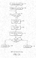
- each pixel may be captured in a number of ways.
- a drive line may be activated, and pickup lines may be turned on and off in a sequence to capture a line of pixels.
- This sequencing may operate as a scanning sequence.
- a first drive line is activated by connecting it to a signal source, and then one pickup line is connected to amplifier/buffer circuitry at a time, the information from the pixel formed at the crossing of the two lines is captured, and then disconnected.
- a next pixel is processed in sequence, then another, then another, until the entire array of pickup lines is processed.
- the drive line is then deactivated, and another drive line is activated, and the pickup lines are again scanned with this active drive line.
- These may be done one at a time in sequence, several non-adjacent pixels may be processed simultaneously, or other variations are possible for a given application. After the grid of pixels is processed, then a rendering of object information will be possible.
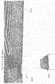
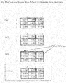
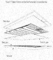
- pickup lines or top plates 102a[m], 102b[m+1] are located on a insulating dielectric substrate layer 104 and configured to transmit a signal into a surface of an object located in close proximity to the sensor lines.
- Drive lines or bottom plates 106a[n], 106b[n+1] are juxtaposed and substantially perpendicular to the drive lines or plates and are located on an opposite side of the a insulating dielectric substrate to form a type of a grid.
- the pickup lines are configured to receive the transmitted electromagnetic fields modified by the impedance characteristics on an object placed within the range of those electric fields.
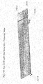
- FIG. 2 a diagrammatic view of a sensor 200 is shown having pickup lines or top plates 202a, 202b and insulating layer 204, and drive lines or bottom plates 206a, 206b.
- the Figure further illustrates how electromagnetic fields 208a, 208b extend between the drive lines and pickup plates through the substrate. Without an object within proximity, the electric field lines are uniform within the sensor structure and between the different lines. When an object is present, a portion of the electric field lines are absorbed by the object and do not return to the pickup plates through the insulating layer.
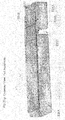
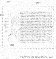
- an object 310 is illustrated proximate the sensor 300.
- the sensor 300 has pickup lines or top plates 302a, 302b, an insulating dielectric layer 304, and drive lines or bottom plates 306a, 306b.
- the drive lines and pickup lines of this device example may be individually activated, where a drive line/pickup line pair is activated to produce an active circuit.
- the result is a circuit that transmits electric field from active drive plate 316 into the combined dielectric of the insulating layer 304 and object 310 via electric field lines, 306a, 306b, and received by the active pickup plate.
- some of the field lines are captured by the object when it is placed about the active electrode pair.
- the variations in an object can be detected and captured electronically by capturing and recording the resulting electric field variations occurring at different crossover locations of the drive and pickup lines. Similar to common capacitance based placement sensors, the sensor can capture a type of image of the object surface electronically, and generate a representation of the features and characteristics of an object, such as the features and characteristics of a fingerprint in the fingerprint sensor example described below.
- a drive line may be activated, and the pickup lines may be scanned one or more at a time so that a line of pixels can be captured along the drive line and pickup lines as they are paired along a line at the crossover locations. This is discussed in more detail below in connection with Figure 5 .
- each area over which a particular drive line overlaps a pickup line with a separation of the a insulating dielectric substrate is an area that can capture and establish a sensing location that defines characteristics or features of a nearby object about that area. Since there exist multiple sensing locations over the area of the sensor grid, multiple data points defining features or characteristics of a nearby object can be captured by the sensor configuration.
- the sensor can operate as a planar two-dimensional sensor, where objects located on or about the sensor can be detected and their features and characteristics determined.
- the embodiment is not limited to any particular configuration or orientation described, but is only limited to the appended claims, their equivalents, and also future claims submitted in this and related applications and their equivalents. Also, many configurations, dimensions, geometries, and other features and physical and operational characteristics of any particular embodiment or example may vary in different applications without departing from the spirit and scope of the embodiment, which, again, are defined by the appended claims, their equivalents, and also future claims submitted in this and related applications and their equivalents .
- a sensor device includes drive lines located on or about an insulating dielectric substrate and configured to transmit a signal onto a surface of an object being sensed.
- Pickup lines arc located near or about the drive lines and configured to receive the transmitted signal from the surface of an object.
- the substrate may act as an insulating dielectric or spacing layer.
- the substrate may be for example a flexible polymer based substrate.
- KaptonTM tape is widely used in flexible circuits such as those used in printer cartridges and other devices.
- the package may include such a flexible substrate, where the drive lines may be located on one side of the substrate, and the pickup lines may be located on an opposite side of the substrate.
- the drive lines may be orthogonal in direction with respect to the pickup lines, and may be substantially perpendicular to the pickup lines.
- a device may be configured with drive lines and pickup lines located on or about opposite sides of an insulating dielectric substrate, where the combination of these three components provides capacitive properties.
- the drive lines may be activated to drive an electric field onto, into or about an object.
- the pickup lines can receive electronic fields that originated from the drive lines, and these electronic fields can be interpreted by processing or logic circuitry to interpret features or characteristics of the object being sensed.
- the layer separating the drive lines from the pickup lines can provide a capacitive property to the assembly.
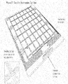
- a grid may be formed.
- the drive lines are located and oriented substantially in parallel with respect to each other about a first plane.
- One surface of the substrate is located about the drive lines in a second plane that is substantially parallel relative to the drive lines.
- the pickup lines are located and oriented substantially in parallel with respect to each other about a third plane that is substantially parallel to the first and second planes and also located about another substrate surface that is opposite that of the drive lines, such that the substrate is located substantially between the drive lines and the pickup lines.
- the embodiment is directed to a sensor configured with plurality of drive and pickup lines that generally cross over each other at a pixel location and are configured to detect presence and other features and characteristics of a nearby object
- the embodiment is not limited to any particular configuration or orientation, but is only limited to the appended claims, their equivalents, and also future claims submitted in this and related applications and their equivalents.
- orientation of the planes (which may be deformable, and thus may be sheets separated by a substantially uniform distance) of groups of components (such as drive lines or pickup lines for example) or substrates may vary in different applications without departing from the spirit and scope of the embodiment.
- a plurality of drive lines are juxtaposed on one surface of a generally planar substrate, and a plurality of pickup lines are juxtaposed on an opposite surface of the planar substrate.
- the drive lines are substantially orthogonal to the pickup lines, and may be described as substantially perpendicular to the pickup lines.
- the distance between the drive lines and pickup lines may be filled with a substrate or insulating material that will provide for a capacitive configuration.
- the drive lines on one side of the substrate forms one capacitive plate, and the pickup lines on an opposite side for the corresponding capacitive plate.
- sensor lines such as sensor drive lines and sensor pickup lines
- substantially parallel drive lines These drive lines are intended to be described as parallel conductive lines made up of a conductive material formed, etched, deposited or printed onto the surface such as copper, tin, silver and gold.
- conductive lines are seldom "perfect” in nature, and are thus not exactly parallel in practice. Therefore, they arc described as "substantially parallel”.
- Different applications may configure some of the drive lines even non-parallel, such that the lines may occur parallel for a portion of the line, and the line may necessarily deviate from parallel in order to connect with other components for the device to operate, or in order to be routed on or about the substrate on which it is formed or traced.
- the separate array of lines may be described as orthogonal or perpendicular, where the drive lines are substantially orthogonal or perpendicular to the pickup lines.
- the various lines may not be perfectly perpendicular to each other, and they may be configured to be off-perpendicular or otherwise crossed-over in different angles in particular applications.
- They also may be partially perpendicular, where portions of drive lines may be substantially perpendicular to corresponding portions of pickup lines, and other portions of the different lines may deviate from perpendicular in order to be routed on or about the substrate or to be connected to other components for the device to operate.
- the drive lines can transmit an electromagnetic field toward an object that is proximal to the device.
- the pickup lines may receive a signal originating from the drive lines and then transmitted through the object and through the substrate and onto the pickup lines.
- the pickup lines may alternatively receive a signal originating from the drive lines that were then transmitted through the substrate and onto the pickup lines without passing through the object.
- This electric field can vary at different locations on the grid, giving a resultant signal that can be interpreted by some type of logic or processor circuitry to define features and/or characteristics of an object that is proximate the assembly.
- the drive lines and pickup lines may be controlled by one or more processors to enable the transmission of the signal to an object via the drive lines, to receive a resultant signal from an object via the pickup lines, and to process the resultant signal to define an object image.
- One or more processors may be connected in one monolithic component, where the drive lines and pickup lines are incorporated in a package that includes the processor.
- the drive lines, pickup lines and substrate may be assembled in a package by itself, where the package can be connected to a system processor that controls general system functions. This way, the package can be made part of the system by connecting with a system's input/output connections in order to communicate with the system.
- the senor can be connected as a stand-alone component that communicates with the system processor to perform sensor operations in concert with the system processor.
- a sensor may be configured to drive signals at different frequencies since the impedance of most objects, especially human tissue and organs, will greatly vary with frequency.
- the receiver In order to measure complex impedance at one or more frequencies of a sensed object, the receiver must be able also to measure phase as well as amplitude.
- the resulting signal generated from a given impedance sensing electrode pair may result from varying frequencies, known in the art as frequency hoping, where the receiver is designed to track a random, pseudo-random or non-random sequence of frequencies.
- a variation of this embodiment could be a linear or non-linear frequency sweep known as a chirp. In such an embodiment one could measure the impedance of a continuous range frequencies very efficiently.
- a grid sensor as described above may be configured to also operate as a pointing device.
- a pointing device could perform such functions as well known touch pads, track balls or mice used in desktops and laptop computers.
- a two dimensional impedance sensor that can measure the ridges and valleys of a finger tip may be configured to track the motion of the fingerprint patterns.
- Prior art swiped fingerprint sensors can perform this function, but due to the physical asymmetry of the array and the need to speed correct, or "reconstruct" the image in real time make these implementations awkward at best.
- the sensor could also double as both a fingerprint sensor and a high quality pointing device.
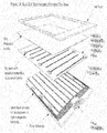
- One device configured according to the embodiment includes a first array of sensor lines on a flexible substrate, and a second array of sensor lines on a flexible substrate, and also a processor configured to process fingerprint data from the first and second arrays of sensor lines.
- the separate sensor lines When folded upon itself in the case of a single flexible substrate or when juxtaposed in the case of separate substrates, the separate sensor lines cross each other without electrically shorting to form a grid with cross-over locations that act as pixels from which fingerprint features can be sensed.
- an array of substantially parallel sensor drive lines is located on a surface of the flexible substrate. These drive lines arc configured to sequentially transmit signal into a surface of a user's finger activating a line at a time.
- a second array of sensor lines is similar to the first, consisting of substantially parallel sensor pickup lines that are substantially perpendicular to the drive lines. These pickup lines arc configured to pick up the signal transmitted from the first.
- the flexible substrate is further configured to be folded onto itself to form a dual layer configuration.
- the first array of sensor drive lines becomes substantially perpendicular to the second array of pickup sensor lines when the flexible substrate is folded onto itself.
- This folding process creates crossover locations between these separate arrays of sensor lines - though they must not make direct electrical contact so that they operate independently.
- These crossover locations represent impedance sensing electrode pairs configured to sense pixels of an object and its sub-features juxtaposed relative to a surface of the flexible substrate. The scanning of these pixels is accomplished by activating individual rows and columns sequentially.
- the perpendicular pickup rows are scanned one at a time over the entire length of the selected driver. Only one row is electrically active (high impedance) at a time, the non active rows are either shorted to ground or multiplexed to a state where they do not cross couple signal.
- a finger ridge is placed above an array crossover location that is active, it interrupts a portion of the electric field that otherwise would be radiated through the surface film from the active drive column to the selected row pickup.
- the placement of an object's subfeature, such as a ridge or valley in the case of a fingerprint sensor, over an impedance sensing electrode pair results in a net signal decrease since some of the electric field is conducted to ground through the human body.
- the valley affects the radiation of electric field from the selected drive line to the selected pickup line much less than a ridge would.
- this general example of the grid sensor will be now used to illustrate how such a sensor configured according to the embodiment can be implemented as a fingerprint sensor, where the object would simply be the surface of the fingerprint on the user's finger.
- This example will be carried through the following Figures for illustration of the benefits and novel features of the impendance sensor configured according to the embodiment.
- any object may be sensed by a device configured according to the embodiment.
- the example and description are intended only for illustration purposes.
- the senor can be configured to detect the presence of a finger surface located proximate to the sensor surface, where the drive lines can drive an active electromagnetic field onto the finger surface, and the pickup lines can receive a resulting electromagnetic field signal from the pickup lines.
- the drive lines can generate an electric field that is passed onto the surface of the finger, and the different features of the fingerprint, such as ridges and valleys of the fingerprint surface and possibly human skin characteristics, would cause the resulting signal to change, providing a basis to interpret the signals to produce information related to the fingerprint features.
- a flexible substrate is used as the insulating dielectric layer 104, to allow for beneficial properties of durability, low cost, and flexibility.
- the drive lines or plates 106a, 106b are located on the flexible substrate and configured to transmit a signal into a surface of a user's fingerprint features and structures, such as ridges and valleys, placed on or about the sensor lines.
- the pickup lines 102a, 102b are configured to receive the transmitted signal from the user's finger surface.
- a processor (not shown) can be configured to collect and store a fingerprint image based on the received signal from the pickup lines.
- an example a sensor 400 configured as an object sensor, where the top plates or pickup lines 402a, 402b, ..., 402n are located on one side of insulating dielectric layer or substrate 404. Bottom plates or pickup lines 406a, 406b, ..., 406n are located on an opposite side of the substrate 404. Electric fields 408a, 408b extend from bottom plates or drive lines 406a, 406b through the insulating layer or substrate 404 and onto active top plate 402a.
- these drive lines may be activated one at a time to reduce any interference effects, but the electric field results illustrated here are intended to illustrate a contrast between electric fields that are partially or fully absorbed by the object with electric fields that are not absorbed the object at all.
- This information may be collected from drive and pickup plate electrode pairs at each crossover location to sense features and characteristics of the object that is proximate the sensor lines.
- Partially covered top plate or pickup line 402b is connected to voltmeter 417, and uncovered top plate 402a is connected to voltmeter 418.
- Active drive line or bottom plate 406b is connected is connected to AC signal source 416, causing an electric field to radiate from active plate 406b.
- the number of drive lines and pickup lines can vary depending on the application, and it may depend on the cost and resolution desired.
- the electric field lines 408a is partially captured by the pickup lines 402a and 402b, and part is captured by the object, in this case finger 410.
- volt meter 417 illustrates the response to the top plate or drive line 402b
- voltmeter 418 illustrates the response of top plate or drive line 402a.
- the difference in the deflections of voltmeter 417 in comparison 418 show the delta in electric field intensity between the two electrode pair locations, one with a finger present the other without.
- FIG. 5 another example of a sensor configured according to the embodiment is illustrated the Drive and pickup configuration when detecting the presence of an object.
- the sensor 500 is illustrated, where the top plates or pickup lines 502a, 502b, ..., 502n are located on one side of insulating layer or substrate 504, and bottom plates or drive lines 506a, 506b, ..., 506n are located on an opposite side of the substrate 504.
- the pickup lines are shown on the layer closest to the object being sensed for maximum sensitivity, and the drive lines shown on the opposite side of the substrate.
- Electric fields 508a, 508b extend from bottom plates or drive lines 506a, 506b through the insulating layer or substrate 504 and onto active top plate 502b.
- Other configurations arc possible, perhaps having drive plates on the top, and pickup plates on the bottom.
- the embodiment is not limited to any particular configuration that is insubstantially different than the examples and embodiments disclosed and claimed herein.
- Figure 5 further shows a snapshot of one selected individual electrode pair located at the crossover of pickup line 502b and drive line 506b, where the remaining pickup and drive lines are not active, shown grounded in Figure 5 .
- Drive line 506b is connected to AC voltage source 516
- pickup line 502b is connected to amplifier/buffer 514.
- electric field lines 508a, 508b are generated, and they radiate from drive line 506b and arc sensed by pickup line 502b, sending the resultant signal into amplifier/buffer 514, and are later processed by analog and digital circuit functions.
- Grounding the inactive adjacent drive and pickup lines focuses the electric fields 508a and 508b at the crossover location between the active the drive and pickup plates, limiting crosstalk from adjacent areas on the object being sensed.
- different drive line/pickup line crossover pairings may be activated to capture different pixels of information from the object.
- an object sensor it can capture information on the shape of the object, and, if the electrical characteristics arc non-uniform across its surface, it's composition.
- the embodiment is not limited to this particular configuration, where one single electrode pair, several electrode pairs, or even all electrode pairs may be active at one time for different operations.
- a drive line may be activated, and the pickup lines may be scanned one or more at a time so that a line of pixels can be captured along the drive line and pickup lines as they are paired along a line at the crossover locations.
- the AC voltage source 516 may remain connected to drive line 506b, and the connection of the amplifier/buffer 516 may cycle or scan over to sequential pickup lines, so that another pixel of information can be captured from another pickup line crossover paired with drive line 506b.
- drive line 506b can be deactivated, than another drive line in sequence can be activated with the AC voltage source, and a new scanning can commence through the pickup lines.
- a two dimensional image or rendering of the object features and characteristics can be made, such as a rendering of the shape of the object, and potentially a composition map.
- a reduced cost fingerprint swipe sensor could be configured using the same innovation provided by the embodiment.
- a reduced number of pickup lines could be configured with a full number of orthogonal drive lines.
- Such a configuration would create a multi-line swipe sensor that would take the form of pseudo two-dimensional sensor, and when a finger was swiped over it would create a mosaic of partial images or slices. The benefit of this would be to reduce the complexity of image reconstruction task, which is problematic for current non-contact silicon sensors that rely on one full image line and a second partial one to do speed detection.
- Figures 6a and 6b illustrate the operation of the sensor when detecting surface features of an object such as fingerprint ridges and valleys.
- the sensor is configured identically to the previous example in Figure 5 , but in this case is interacting with a textured surface such as a fingerprint.
- FIG. 6a and b another example of a sensor configured according to the embodiment is illustrated.
- the sensor 600 is illustrated, where the top plates or pickup lines 602a-n are located on one side of insulating layer or substrate 604, and bottom plates or drive lines 606a-n arc located on an opposite side of the substrate 604.
- For maximum sensitivity pickup lines are shown on the layer closest to the object being sensed, and the drive lines shown on the opposite side of the substrate.
- Figure 6a shows electric field lines 620 as they interact with a proximally located object's valley and Figure 6b shows electric field lines 621 as the interact with a proximally located object's peaks, extending from bottom plate drive line 606b through the insulating layer or substrate 604 and onto active drive line 606b.
- the corresponding ridges and valleys over the fingerprint surface can be captured by the grid of drive line/pickup line crossover points, and the resulting data can be used to render an image of the fingerprint.
- a stored fingerprint can then be compared to the captured fingerprint, and they can be compared for authentication. This is accomplished using any one of many fingerprint matching algorithms which are available from vendors as stand alone products. Such vendors include Digital Persona, BioKey, and Cogent Systems, to name just a few.
- FIG. 6a and b Also illustrated in Figures 6a and b , is the individual sensor line pairing of pickup line 602b and drive line 606b. Their crossover forms the active electrode pair, and the remaining pickup and drive lines are not active, and will nominally be grounded by electronic switches.
- Drive line 606b is connected to AC voltage source 616, and pickup line 602b is connected to amplifier/buffer 605.
- electric field lines 620 and 621 are created as shown in Figures 6a and 6b respectively, and they emanate between the drive line 606b and pickup line 602b, sending a resultant signal that is radiated onto pickup line 602b and connected to amplifier/buffer 605, and later processed by analog and digital processing circuitry.
- different drive line/pickup line crossover pairs may be activated to capture different pixels of information from the object.
- a fingerprint it can capture information on different features and characteristics of the fingerprint and even the body of the finger itself.
- the embodiment is not limited to this particular configuration, where one electrode pair, several electrode pairs, or even all electrode pairs may be active at one time for different operations. In practice, it may be preferable for less than all of the electrode pairs to be active at a given time, so that any interference that may occur between close-by pixels would be minimized.
- a drive line may be activated, and the pickup lines may be scanned one or more at a time so that a line of pixels can be captured along the drive line and pickup lines as they are paired along a line at the crossover points.
- the voltage source 616 may remain connected to drive line 606b, and the connection to buffer/amplifier 605 may cycle or scan over to another pickup line, so that another pixel of information can be captured from another electrode pair using driveline 606b.
- drive plate 606b remains excited by AC signal source 616 until an entire column of pixels is scanned, while unused drive plates (606a,c-n etc.), are switched to ground for isolation purposes. Likewise, in one embodiment only one pickup plate is active at a time and some or substantially all other pickup plates are switched to ground to minimize crosstalk.
- the scanning process continues beyond the snapshot shown in figures 6a and 6b , with the next column in sequence being activated, 606c, (although the sequence could be arbitrary), Once the entire sequence of Pickup Plates 602a-n is scanned, the next driver line 606d would activated, until all, or substantially all of the drive lines 606a-n have been sequenced. Once all the drive columns have been activated and the pickup plates scanned for each column, one will have collected a complete two dimensional array of pixels equal to the number of driver rows times the number of pickup columns. For a 500 DPI sensor that would create a 10x10mm array or100mm 2 , consisting of 40,000 individual pixels. Depending on the application, all of the drive lines may be sequenced, or possibly some or most of them may be sequenced.
- the two conductive layers Drive layer 606 and Pickup layer 602 arc separated by an electrically insulating layer 604.
- This insulating layer 604 has high DC resistance and has a dielectric constant greater than one to allow the transmission of high frequency electric fields through it.
- this layer 602 is created by folding a single sided flexible printed circuit board back onto itself. In another embodiment it is created by placing a dielectric layer between two electrically active layers to form a double sided circuit board.
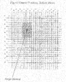
- Figure 7 shows an example of an x-y grid of plate rows and columns depicted by lumped circuit components that represent the electric field couplings of the sensor at each drive/pickup crossover.
- the bottom plates 701a,b,c etc. are driven one at a time by AC signal source 716 via switch matrix 740a-n.
- Figure 7 shows a scan snapshot where one drive switch 740b in the on condition connecting the corresponding plate to the signal source. This activates one entire row 740b with AC signal over the entire length of the plate that is equal to the sensor width in one dimension.
- each column plate 703a,b,c etc. will pickup up AC signal through insulating layer 704 and coupling capacitors 761a,b,c ...n. Only one pickup plate at a time is active being switched into the buffer amplifier 716.
- Top Plate 702b is shown as the active plate in Figure 7 , while all or substantially all other pickups are shorted to ground via switch matrix 730a-n, thus the information from one x-y pixel is captured.
- a single row remains active only as long as it takes the entire number of pickup plates/columns to be scanned.
- Scan time per pixel will depend on the frequency of operation and the settling time of the detection electronics, but there is no need to scan unduly fast as is typical with prior art swipe sensors.
- prior art swipe sensors must scan at a very high pixel rate in order not to lose information due to undersampling relative to the finger speed that can be greater than 20cm/sec. This reduction in capture speed relative to a swipe sensor relaxes the requirements of the analog electronics and greatly reduces the data rate that a host processor must capture in real time. This not only reduces system cost but allows operation by a host device with much less CPU power and memory. This is critical especially for mobile devices.
- the amount of signal that is coupled into the buffer amplifier 716 is a function of how much capacitance is formed by the insulating layer and the finger ridge or valley in close proximity.
- the detailed operation of how these electric fields radiate is shown in Figures 6a and b.
- the total coupling capacitance is a series combination of the insulating layer capacitance 704 that is fixed for a given thickness, and the variable topological capacitance of the object being sensed.
- the variable portion of this is shown in Figure 7 as a series of variable capacitors numbered 760a-n, 761a-n, 762a-n etc., forming a two dimensional array.
- Figure 8 shows an example of an embodiment of the placement sensor using a differential amplifier 880 to take the signal from the selected pickup plate (802a-n), and subtract it from the reference signal of plate 805.
- the electrical subtraction of these signals performs several functions: first wide band common mode is subtracted out; second, subtracting against reference plate 805 provides a relative reference signal equivalent to an ideal ridge valley; third, common mode carrier signal that couples into both plates other than through a finger is also subtracted out.
- First order carrier cancellation of etch variation in the pickup plates also occurs when we subtract out carrier that is coupled in by other means than through fingers placed on the sensor. This is critical for high volume manufacturing at a low cost.
- Reference plate 805 is intentionally located outside of the finger contact area of the sensor, separated from pickup plates 802a-n by Gap 885, Gap 885 is much larger that the nominal gap between the pickup plates that is typically 50um. In a real world embodiment plate 805 would be positioned under the plastic of a bezel to prevent finger contact, placing it at least 500um apart from the other pickup plates.
- Each one of the pickup plates 802a-n is scanned sequentially being switched through pickup switches 830a-n connecting them to Differential Amplifier 880.
- the positive leg of the differential amplifier remains connected to reference plate 805 to provide the same signal reference for all of the pickup plates.
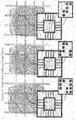
- Figure 9a shows a circuit diagram of an example of a front end for the placement sensor in a topology that uses a bank of Single Pole Double Throw Switches or SPDTs to scan the pickup plate rows and a bank of Single Pole Single Throw switches to multiplex the pickup plate columns.
- SPDTs Single Pole Double Throw Switches
- Each SPDT has a Parasitic Capacitance 945, due to the fact that real world switches to not give perfect isolation. In fact the amount of isolation decreases with frequency, typically modeled by a parallel capacitor across the switch poles.
- a SPDT switch we can shunt this capacitance to ground when an individual plate is not active. Since there is a large array of switches equal to the number of pickup plates, typically 200 for a 500dpi sensor, the effective shunt capacitance to ground is multiplied by that number. So if a given switch has 0.5 picofarads of parasitic capacitance and there where 200 pickups, that would add up to 100 picofarads of total shunt capacitance.
- a compensating circuit In order to prevent this large capacitance from diverting most of the received signal from the active pickup to ground, it is desirable in this example to use a compensating circuit. This is accomplished by using resonating inductor 939, forming a classic bandpass filter circuit in conjunction with parasitic capacitors 945 (one per switch) and tuning capacitors 934 and 937. A two step null & peak tuning calibration procedure is used where tuning capacitor 934 and 937 are individually tuned with inductor 939 using the same drive signal on both the plus and minus inputs to differential amplifier 980. The two bandpass filters formed with inductor 1039 and resonating capacitors 934, and 937 respectively, will be tuned to the same center frequency when there is zero signal out of differential amplifier 980.
- capacitors 934 and 937 and inductor 939 are tuned together using a differential input signal with opposite 180 degrees phases on the plus and minus inputs to the differential amplifier 980. They are incremented in lock step until the exact drive carrier frequency is reached, this occurs when the output of differential amplifier 980 is at its peak, making the center frequency equal to the exact frequency of the carrier drive signal 916.
- a calibration routine would be performed before each fingerprint scan to minimize drift of this filter with time and temperature.
- the resonating inductor 939 needs to have a Q or Quality Factor of at least 10 to give the filter the proper bandwidth characteristics necessary to optimize the signal to noise ratio.
- carrier source 916 may be a variable frequency source, and capicitors (937 and 934) may be fixed values. In this embodiment, tuning is accomplished by varying the frequency of source 916) until peak output is obtained from differential amplifier 980
- Figure 9b shows an alternate example of a device employing multiple banks of plates grouped together, each with their own differential amplifiers.
- Dividing up the large number of parallel pickup plates into groups each containing a smaller number of plates is an alternate architecture that would not require the use of a tuned bandpass filter in the front end because the parasitic switch capacitances would be greatly reduced. This would have two possible advantages, first lower cost, and second the ability to have a frequency agile front end.
- first switch 944a of bank 907a is active. All other switch banks 907a -907n are shown inactive, shorting their respective plates to ground.
- voltage or current differential amplifier 980a has any plate signal conducted into it
- voltage or current differential amplifier 980b -980n have both their positive and negative inputs shorted to ground through their respective switches 945a-n and 945r, preventing any signal from those banks making a contribution to the overall output.
- Each of the differential amplifiers 980a -980n is summed through resistors 987a-987n into summing amplifier 985. Only the differential amplifier 980a in this snapshot has plate signal routed into it, so it independently produces signal to the input of summing amplifier 985. This process is repeated sequentially until all or substantially all of the switch banks 907a-n, and switch plates 944a-n, 945a-n, etc, of the entire array are fully scanned. In different embodiments, all or substantially all of the array may be scanned, or less than the entire array may be scanned in different applications. In some applications, a lower resolution may be desired, so all of the array may not need to be scanned.
- a full image may not be necessary, such as a navigation application, where limited images may be used to detect movement of speed, distance and/or direction to use as input for a pointing device, such as directing a cursor on a display similar to a computer touch-pad or a mouse.
- the capacitive input load on each plate is reduced from that of the full array of switches to the number of switches within a given plate group. If we were to divide for example 196 potential pickup plates into 14 banks of 14 plates, resulting in a capacitance load equal to the parasitic capacitance of 14 switches (944), plus the capacitive load of the differential amplifier. If analog switches 944 are constructed with very low parasitic capacitance then the overall input load would be small enough not to need a bandpass circuit in the front end in order to resonate out the load capacitance. As integrated circuit fabrication techniques improve we would be able design smaller switches with less parasitic capacitance, making this approach become more attractive.
- Figure 9c illustrates another example of a front end circuit using individual plate buffers that are multiplexed into a second stage differential amplifier.
- Buffers 982a through 982n as illustrated are special buffers that are designed to have very low input capacitance.
- these buffers could be configured as single stage cascoded amplifier in order to minimize drain-to-gate Miller capacitance and die area.
- two sets of switches could be used for each input.
- Analog switches 930a-930n are included in this example to multiplex each selected buffer into differential amplifier 980.
- Switches 932 are included to shut down the power simultaneously to all the other input buffers that are not selected. This effectively puts them at ground potential.
- An alternate embodiment would be to put input analog switches in front of each amplifier to allow a short of the unused plates directly to ground.
- One effect of this approach may be an increase in input load capacitance for each plate.
- Figure 9c shows a snapshot of the scanning process where top plate 902a is being sensed though buffer 982a that has power supplied to it through switch 932a.
- Analog switch 930a is closed, routing it to differential amplifier 980. All other buffer outputs are disconnected from the differential amplifier 980 via analog switches 930b-n and power switches 982b-n
- differential amplifier 980 The positive input to differential amplifier 980 is always connected to the reference plate 902r, providing an "air" signal reference to the amp.
- the differential amplifier 980 serves to subtract out noise and common mode carrier signal in addition to providing a "air" reference carrier value.
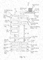
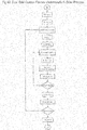
- Figure 10 shows a particular embodiment of a placement sensor implemented with traditional analog receiver technology.
- the analog front end begins with Differential Amplifier 1080 where selected Pickup Plate 1002a-n is subtracted from Reference Plate 1005, which is located outside the finger contact area providing a reference signal equivalent to an ideal finger valley.
- a programmable gain stage or PGA 1090 follows the Differential Amplifier 1090, but could be integrated into the same block providing both gain an subtraction in a single stage.
- PGA 1090 is designed to have a gain range wide enough to compensate for production variations in plate etching and solder mask thickness between the layers.
- Control processor 1030 orchestrates the scanning of the two dimensional sensor plate array.
- Drive plates/columns 1002a - 1002n are scanned sequentially by the Drive Plate Scanning Logic 1040 in the Control Processor 1030.
- a selected drive plate When a selected drive plate is activated it is connected to carrier signal source 1016. All inactive drive plates are connected to ground. Before activating the next drive plate in the sequence the active drive plate remains on long enough for the entire row of Pickup Plates 1002a-n to be scanned by Pickup Plate Logic 1045.
- Analog mixer 1074 multiplies the gained up plate signal against the reference carrier 1013. The result is a classic spectrum of base band plus harmonic products at multiples of the carrier frequency.
- An analog low pass filter 1025 is employed to filter out the unwanted harmonics and must have a sharp enough roll of to attenuate the information associated with of the second harmonic without losing base band information.
- A/D Converter 1074 Following the low pass filter is an A/D Converter 1074 that must sample at a least twice the pixel rate to satisfy the Nyquist criteria.
- Memory buffer 1032 stores the A/D samples locally with sufficient size to keep up with the worst case latency of the host controller.
- the A/D Sample Control Line 1078 provides a sample clock for the converter to acquire the sequential pixel information that is created by the sequencing of the plate rows and columns.
- Figure 11 shows an example of one embodiment of a placement sensor implemented with direct digital conversion receiver technology.
- the analog front end begins with Differential Amplifier 1180 where selected Pickup Plate 1102a-n is subtracted from Reference Plate 1105, which is located outside the finger contact area providing a reference signal equivalent to an ideal finger valley.
- the electrical subtraction of these signals performs several functions: first wide band common mode is subtracted out; second, subtracting against reference plate 1105 provides a relative reference signal equivalent to an ideal ridge valley; third, common mode carrier signal that couples into both plates other than through a finger is also subtracted out. Elimination of common mode is particularly important in high RF noise environments. First order carrier cancellation of etch variation in the pickup plates also occurs when we subtract out carrier that is coupled in by other means than through fingers placed on the sensor. This is critical for high volume manufacturing at a low cost.
- a programmable gain stage or PGA 1190 follows the Differential Amplifier, which could easily be combined into a single differential amplifier including programmable gain as is commonly done in modern integrated circuit design PGA 1190 is designed to have a gain range wide enough to compensate for production variations in plate etching and solder mask thickness between the layers.
- Control processor 1130 orchestrates the scanning of the two dimensional sensor plate array.
- Drive plates/columns 1102a - 1102n are scanned sequentially by the Drive Plate Scanning Logic 1140 in the Control Processor 1130.
- a selected drive plate When a selected drive plate is activated it is connected to carrier signal source 1116. All inactive drive plates are connected to ground. Before activating the next drive plate in the sequence the active drive plate remains on long enough for the entire row of Pickup Plates 1102a-n to be scanned by Pickup Plate Logic 1145 and captured by the A/D converter 1125.
- the A/D Converted 1125 is sampled at a rate of at least twice the carrier frequency to satisfy the Nyquist criteria.
- the A/D Sample Control Line 1107 provides a sample clock for the converter to acquire the sequential pixel information that is created by the sequencing of the plate rows and columns.
- a Digital Mixer 1118 that digitally multiplies the A/D output that is at the carrier frequency against the reference carrier generated by the Digitally Controlled Oscillator 1110. The result is that the signal is down converted to the base band with the carrier removed. There are other unwanted spectral components created by this process, namely a double time carrier side band, but these can easily be filtered out.
- a combination decimator and digital filter 1120 follows the Digital Mixer 1118. This block performs sampling down conversion, reducing the sample rate from at least twice the carrier frequency to at least twice the pixel rate that is much lower.
- the digital filter would typically include a Cascaded Integrator Comb, or CIC filter, which removes the unwanted spectral byproducts of mixing as well as improving the receiver signal to noise.
- a CIC filter provides a highly efficient way to create a narrow passband filter after mixing the signal down to baseband with the digital mixer.
- the CIC filter may be followed by a FIR filter running at the slower decimated rate to correct passband droop.
- a relatively small Control Processor Buffer (1132) could be used to capture and entire fingerprint.
- a 200x200 array producing 40k pixels could be stored in a 40kb buffer.
- a swipe sensor that must scan the partial image frames at a rate fast enough to keep up with the fastest allowable swipe speed, usually around 200ms.
- a slow swipe of two seconds must also be accommodated, requiring ten times the amount of memory as the fastest one.
- Various techniques have been developed to throw away redundant sample lines before storage, but even with that the real time storage requirements arc much greater for swipe sensors. This is a critical factor in Match on Chip applications where memory capacity is limited.
- a placement sensor has no real-time data acquisition or processing requirements on the host processor beyond the patience of the user for holding their finger in place.
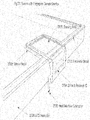
- Chip on Flex is a configuration where a processor chip is attached to a flexible substrate, such as KaptonTM tape, and that is electrically connected to conductive lines and possibly other components located on the flexible substrate.
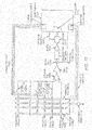
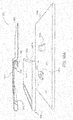
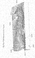
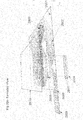
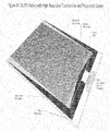
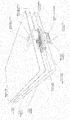
- the sensor layout 1200 is shown within the borders of Kapton tape having pitch rails 1202, 1204 with slots 1206 located along both rails. These slots are used in the manufacturing process to feed the tape through the process while lines and possibly components are formed on the tape.
- the pitch of a device refers to the length of Kapton tape required to form a device on the CoF.
- the distance "d” 1208, measured here between slots 1207 and 1209, is substantially constant throughout each rail, and the pitch is a shorthand method of determining the length of flex that a device covers.
- the pitch 1212 shows a span between slot 1207 and 1214 of eight slots, and thus would be characterized as an 8-pitch device.
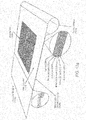
- the example sensor device shown which may be a fingerprint sensor or other type of placement, 2D or area sensor, illustrates an integrated circuit 1210, which may be a logic circuit formed on a silicon substrate, a microprocessor, or other circuit for processing pixel information captured from a sensor circuit.
- the example may also be formed or otherwise manufactured on a substrate other than flexible substrate or Kapton tape, in fact it may be formed on a silicon substrate, rigid board, or other substrate configured for various applications.
- integrated circuit 1210 may be a mixed signal chip that enables all or some of the functions described in Figure 16 below. In one embodiment, it has enough inputs and outputs to drive a 200 by 200 line array of drive and pickup lines, and may have more or less of either lines.
- the top layer 1220 is formed by an array of pickup lines connected directly to integrated circuit 1210. This may be a flip chip mounted directly to the flex substrate without bond wires.
- the bottom layer is formed by folding the single layer back onto itself along the folding axis 1230 to create double layer active sensor area 1255. The drive lines fold to create the bottom layer 1225.
- the drive lines in this example are split into left and right groups 1240 and 1242 respectively for the sake of layout balance, but could be all on the left or right side of the sensing area.
- the left drive plate bundles 1240, and right drive plate bundles 1242 are inter-digitated with alternating left and right feeds to form a continuous line array on bottom layer 1225.
- Flexible substrate based connector 1235 routes power, ground and interface signals out to an external host or onto another substrate that contains system level components, such as those illustrated in Figure 16 and described below. These components may include but are not limited to a processor with memory, logic enabling imbedded matching algorithm(s) and encrypting/decrypting functions.
- connector 1235 may be attached to the host substrate using conductive adhesive otherwise known as anisotropic conductive film (ACF attach), which may be labeled as "high density" in some products.
- ACF attach anisotropic conductive film
- FIG. 12B another example of a sensor 1250 is shown having a different orientation and configuration on a substrate. Similar to the above example, the sensor 1250 is a placement sensor, and is configured to be folded onto itself along the folding axis 1251 to create two layers, the bottom layer 1252 with drive lines 1256, and top layer 1254, with pickup lines 1257, integrated circuit 1258, flex external connections 1262, and processor connections 1260 that may be used to connect the integrated circuit to external devices, such as for manufacturing testing for example.
- This configuration however, has a much smaller pitch, again where the distance "d" is the distance between each pair of slots 1206, and the pitch in this example is between slots 1270 and 1272, making this device a 5-pitch device.
- This example device takes up 5 pitches of Kapton tape compared to the other example device 1200 ( Figure 12A ) taking up 8 pitches of Kapton tape.
- This device performs substantially the same function as that of example 1200, Figure 12A , yet takes up less Kapton tape, saving in material costs.
- the device may take up even less pitches of tape if the size of the resulting sensor surface were reduced, allowing the space needed to accommodate the pickup lines, drive lines, and other components to be reduced.
- the effective sensor surface may be ten square millimeters, and could be reduced to nine or even eight millimeters, and the structures could be reduced accordingly to reduce the overall area of the device, likewise reducing the area of substrate required to accommodate the overall device.
- the flex layer structure 1300 includes an imaging area 1350, in which drive lines form crossover locations with pickup lines, where the crossover locations are formed by folding the top layer 1370 over bottom layer 1372, folding the flexible substrate upon itself about flex bend radius 1374.
- the top flex 1364 is layered over top soldermask 1362, which is layered upon top copper or pickup lines 1360.
- Bottom layer solder mask 1370 is folded under top copper 1360, and bottom copper 1372 is formed under solder mask 1370 and over bottom flex 1375.
- FIG. 13b an example of a module structure 1301 is shown for mounting the flex layer structure 1300 of Figure 13a .
- the example structure 1301 includes rigid substrate 1330 that receives the flex top layer 1370 on its top layer with flex locating pins or plastic frame 1337 configured to ensure alignment of the drive plates with the pickup plates.
- the x-y alignment tolerance requirements may be on the order of several pixels, rather than the sub-pixel alignment tolerances that would be required if there were features to be matched between the two layers.
- the four mounting holes (1337) on each layer are sufficient to ensure angular and x-y alignment. Also illustrated is driver chip 1310 and imaging area 1350.
- a sensor device may be incorporated into a system, or may be configured as a stand-alone product.
- the sensor components may be encased in a housing (not shown), and electrical connections exposed for connection to a device or system that would utilize such a device.
- a housing not shown
- electrical connections exposed for connection to a device or system that would utilize such a device Those skilled in the art will immediately see how a sensor configured according to the embodiment as described herein can be incorporated into a housing such as those that widely used in different industry sectors.
- the mechanical connections, designs and structures may necessarily vary according to a particular application.
- FIG. 14 illustrates a diagrammatic representation of a system 1400 that incorporates a sensor 1402 configured according to the embodiment with the folded flexible or rigid substrate 1404 having a top layer 1406 and a bottom layer 1408, and each having either pickup lines or plates and drive lines or plates respectively depending on the application, though not shown here.
- the two-dimensional sensing area 1411 is shown with an object 1410 on top, which may be a finger in the case of a fingerprint sensor, or another object in another application.
- the top layer's pickup plates or lines (not shown) communicate with top plate processing circuitry 1410 via communication link 1412 to send resultant signals received.
- Drive lines or plates are located but not shown here on bottom layer 1408, and receive drive signals from bottom plate processing circuitry 1414 via communication line 1416.
- the top plate processing circuitry 1410 includes front end buffers and amplifiers 1416 configured to receive, amplify and/or buffer or store a resultant signal received from the pickup plates or lines.
- a switch array 1418 such as that illustrated in Figure 9 is configured to receive the signal from the front end 1416 and send the switched signal to analog to digital (A/D) converter 1420 for conversion to a digital signal.
- Digital signal processor (DSP) 1422 is configured to receive the digital signal from A/D converter 1420 and process the signal for transmission.
- Bottom plate processing circuitry 1414 is configured to produce a drive signal for use by drive plates or lines located on the bottom layer 1408 of the sensor substrate 1404, and includes drivers and scanning logic 1424 for producing the signal, and programmable frequency generate 1426 for programmable setting the frequency in which the drive signal is set.
- the bottom plate processing circuitry 1414 includes communication link 1428, likewise, top plate circuitry has communication link 1420 for communicating with system buss 1432 for sending and receiving communications among the system, such as to processors, memory modules, and other components.
- System buss 1432 communicates with persistent memory 1434 via communication link 1436 for storing algorithms 1428, application software 1440, templates 1442, and other code for persistent and frequent use by processor 1444.
- Processor 1444 includes processor logic having logic and other circuitry for processing signals received from the system buss and originating from the sensor 1402, and also includes arithmetic logic unit 1450 configured with logical circuits for performing basic and complex arithmetic operations in conjunction with the processor.
- Processor memory 1452 is configured for local storage for the processor 1444, for example for storing results of calculations and retrieval for further calculations.
- drive signals are controlled by processor 1444, and parameters for the drive signals originating from bottom plate processing circuitry 1414 are set in the bottom plate processing circuitry 1414 by the processor 1444.
- Drive signals are generated by logic 1424 within the parameters set in generator 1426 and sent to bottom plate 1408 via communication link 1416. These signals generate electromagnetic fields that extend to pickup lines on top layer 1406 about the sensing area 1411. These signals are cycled through different pixel electrode pairs on the sensor grid (not shown here, but described above.), and some of these electromagnetic fields arc absorbed by the object 1410 (such as a fingerprint for example). The resultant signal is picked up by the pickup plates or lines located on top layer 1406 about the sensing area (not shown here, but described above.).
- the resultant signal is then transmitted to top plate processing circuitry 1410 via communication line 1412, and the signal is processed and transmitted to storage or processor 1444 for further processing.
- data related to features and characteristics of the object can be defined and utilized by the system.
- the image may be a fingerprint image that can be compared to a stored fingerprint image, and, if there is a match, it can be used to validate a user.
- Figure 15 Illustrates how a device configured according to the embodiment may be applied to a fingerprint sensing application.
- a user places a finger with fingerprint (1510) over the sensor grid, which is formed by the crossover locations of the drive plates (1506a-1506n) and the pickup plates (1502a-1502m).
- Image pixel 1561a senses the fingerprint area above the electrode pair of drive plate 1506a and pickup plate 1502a
- pixel 1561a senses the crossover of drive 1506n and pickup 1502a
- pixel 1562n senses the area above the crossover of drive 1506n and pickup 1502m
- Figure 16 illustrates the steps required to collect the fingerprint image as shown in Figure 15 , using the embodiment shown in Figures 11 and 14 .
- Image capture begins at step 1601.
- a row counter is initialized to 1 at step 1602.
- Step 1603 is the beginning of a row scan sequence.
- a column counter is set to 1 at step 1603.
- the top plate scanning logic 1145 activates the appropriate analog switch (one of 1103a through 1103n) for the selected row.
- Step 1605 the sense of an individual pixel begins when the bottom plate scanning logic 1140 activates the appropriate drive plate (one of 1106a through 1106n) with the carrier signal 1116.
- step 1606 the signal from differential amplifier 1180 is sampled repeatedly by A/D converter 1125 after processing through programmable gain amplifier 1190.
- Digital mixer 1118 mixes the samples down to the baseband frequency set by digital oscillator 1110.
- the baseband signal is then filtered by digital decimating filter 1120 to produce a signal level value for the current pixel.
- the functions performed for this step in the embodiment of Fig 11 could alternatively be performed by the corresponding analog receiver shown in Fig 10 , or other functionally similar arrangements.
- step 1607 the signal level value derived in step 1606 is stored in the appropriate position in memory buffer 1132 that corresponds to the currently selected row and column.
- step 1608 the column number is incremented, and in step 1609 the column number is tested to determine whether the current row collection has been completed.
- step 1605 we collect the next pixel in the row. If the row is complete, we proceed to step 1610 and increment the row number. In step 1611, we test the row number to determine if all the rows have been scanned. If not, flow returns to 1603 to start the next row back at the first column. Once all the rows have been scanned, image capture is complete, and we proceed to step 1612, at which point the image is ready for further processing or transfer to long term storage.
- row and column scanning order may not correspond directly to physical position in the array, as some implementations may more optimally be sample in interleaved fashions.
- FIG 17 an example, of the example as shown in Figure 14 in a user authentication application.
- a system level application 1440 on processor 1444 requires user authentication.
- the user is prompted to provide a finger for verification.
- the system waits for finger presence to be detected in step 1703. This can be performed by collecting a reduced size image as described in Figure 16 and testing for finger image, or via other dedicated hardware. Once finger presence is detected, a complete image is collected in step 1704, using the method described in fig 16 or other substantially similar method.
- step 1705 This image is then stored and in step 1705 converted into a template 1712 as shown in Figure 17B , typically consisting of a map of minutia point locations and types (such as bifurcations 1710, and terminations 1711), or possibly of ridge frequency and orientation, or some combination of both.
- the template is then compared against one or more enrollment templates that were retrieved from persistent template storage 1142 in step 1706. If a match is found, the user is authenticated in step 1708 and granted access to the application. If no match is found, the user is rejected in step 1709, and access is denied.
- a device such as a smartphone may have differing security and convenience (speed) requirements for differing operating modes, as well. These tradeoffs may be governed by the value of security for different types of information. As an example, users may place a low value on security for simply powering up their smartphone or other device. But, they may place a much higher value on performing a financial transaction or other sensitive transfer.
- the amount of time a user would find acceptable to unlock the phone for a simple call would be much shorter than the time they would wait to secure a high value transaction, where a user may be more tolerant of a higher time demand for authenticating the user for a financial transaction.
- Embodiments described herein facilitate supporting both of these requirements by providing variable captured image resolution and matching algorithm security level.
- the image capture procedure described in Figure 16 and the match procedure described in Figure 17A-B may operate in full resolution mode.
- the fingerprint image may be acquired in a half-resolution mode by skipping every other column and every other row - for example where steps 1608 and 1610 would increment the Column and Row counters, respectively, by two instead of one. This may result in an image with half the resolution in each axis compared to the high security mode, and one-fourth the size.
- step 1707 This could cut by a factor of four both the time required to acquire the image ( Figure 16 ) and the time required to extract the template from the image (step 1705). Due to the reduced resolution of the image, and the relaxed security requirements for this convenience mode, the matching threshold applied in step 1707 may be accordingly reduced.
- FIG. 18A-D another embodiment of a sensor module or assembly is illustrated as a sensor 1800, first shown in an expanded view in Figure 18A , made up of a folded flex sensor 1802, a module folding base 1804 and mounting board 1806.
- a switch having a plunger 1812 and base 1813 is incorporated into a sensor assembly that allows the integration of the sensor operations, such as fingerprint sensor operations, together with other operations of a device.
- this assembly allows for the configuration of a personalization switch for use on a device, such as a mobile telephone or smart phone for example, that has extended functions including biometric operations.
- a fingerprint sensor can be used for authentication while using these personal devices.
- the authentication can be used to access the device entirely, access different levels of information such as different information that a user wishes to protect, or could be used for authentication of the user for financial transactions that require a higher level of security.
- These settings maybe preset by the manufacturer, may be reset by the user, may be set by a financial institution associated with the user or the device, or may be configurable by anyone with an interest in protecting the information.
- the folded flex sensor 1802 may be folded at 1805 and 1807 respectively to fit about the module folding base 1804 at mounting locations loop brace 1805-A and folding edge 1807-A respectively, along with placement holes 1808 to aid in placing the flex about the module and holding it in place.
- the sensor 1802 may include processor 1810 as described in similar embodiments above.
- Mounting board 1806 includes a switch 1813 mounted about switch opening 1811 to accommodate plunger 1812, and may also have a processor opening 1814 configured to accommodate processor 1810.
- FIG. 18B another expanded view of the sensor of Figure 18A is shown from another angle, where one side of the flex sensor 1802 shows more clearly the openings 1808 and processor 1810, where the openings 1808 are configured to receive placement or mounting pegs 1816 for holding the sensor 1802 substrate in place and then received by mounting openings 1818.
- the placement or mounting pegs 1820 are received by mounting openings 1822.
- Switch base opening 1824 is configured to receive switch base 1813.
- the opening for the plunger 1812 and the base 1813 may be a single sized opening that will accept the entire switch, or the switch may have base with the same diameter as the plunger so that a single cylindrical or rectangular or other shaped opening may be sufficient to accommodate the switch.
- Figure 18C shows a side cut away view of the assembled sensor assembly with the sensor substrate 1802 mounted on module folding base 1804 and mounted on base 1806, and with the openings 1811 and 1824 accommodating the switch plunger 1812 and switch base 1813 respectively.
- Figure 18D shows a close-up view of the side view of Figure 18C .
- FIGS 19A-J show an alternative sensor/switch assembly where a dome switch is used for the underlying switch that is integrated in the assembly.
- the assembly 1900 includes a dome switch 1912 integrated with module folding base 1904 mounted on mounting board 1906.
- a switch having a domed shaped plunger 1912 and base 1913 ( Figure 19C ) is incorporated into a sensor assembly that allows the integration of the sensor operations, such as fingerprint sensor operations, together with other operations of a device.
- the folded flex sensor 1902 may be folded at 1905 and 1907 respectively to fit about the module folding base 1904 at mounting locations loop brace 1905-A and folding edge 1907-A respectively, along with placement holes 1908 ( Figure 19D ) to aid in placing the flex about the module and holding it in place.
- the sensor 1902 may include processor 1910 as described in similar embodiments above.
- Mounting board 1906 includes a switch 1913 mounted below plunger 1912, and may also have a processor opening 1914 configured to accommodate processor 1910 ( Figure 19D ).
- FIG. 19G H and I, side views of the sensor is shown, showing the flex sensor 1902 and the openings 1908 and processor 1910, where the opening 1908 are configured to receive placement or mounting pegs 1916 for holding the sensor 1902 substrate in place and then received by mounting openings 1918.
- the placement or mounting pegs 1920 are received by mounting openings 1922.
- Switch base opening 1924 is configured to receive switch base 1913.
- the opening for the plunger 1912 and the base 1913 may be a single sized opening that will accept the entire switch, or the switch may have base with the same diameter as the plunger so that a single cylindrical or rectangular or other shaped opening may be sufficient to accommodate the switch.
- Figure 19E,F , and J show a normal, cutaway, and expanded cut away views of the sensor assembly mounted in a device such as a smartphone, with the sensor substrate 1902 mounted on module folding base 1904 and mounted on base 1906, and with the openings 1911 and 1924 accommodating the switch dome plunger 1912 and switch base 1913 respectively.
- the sensor area 1901 is accessed by a bezel opening 1909 which is incorporated into the finished case 1925 of the device. When the user places a finger on sensor surface 1901 they will simultaneously depress switch plunger 1912.
- Figure 20 illustrates a perspective view of one embodiment of an embedded switch 2000 that can provide a means to electronically connect a top conductive layer 2002 through insulating layer 2004 to conductive layer 2006 upon the touch of a user on the surface of the sensor, not shown here, but it may be a layer above conductor 2002.
- the three layers may be embedded within a fingerprint sensor as described above, allowing for a switch located within the double-layered fingerprint sensor, so that a user can activate a function upon touch, such as power, select, initiate, enter, or other switch functions in a device.
- the three layers may be placed on a surface 2006 of module 2008, where the module is located on the surface 2010 of a substrate 2012.
- Figures 21A and 21B Figure 21A shows an embodiment where a switch is formed on the same substrate as the sensor.
- the figures show the folded flex stack-up consisting of flex substrates 2102 and 2103, typically but not limited to Kapton ⁇ , metalized layers 2104 and 2105 are typically etched or formed copper traces and insulating layers 2106 and 2107 are typically solder mask. Insulating layers 2106 and 2107 have a cutout section 2110 out exposing the conductive layers 2104 and 2105. When no vertical pressure is applied over the gap 2110 conductive layers 2104 and 2105 are not electrically in contact with each other and arc in the off position.
- Figure 21B shows the flex top layer 2103 and conductive layer 2112 mechanically depressed by a contacting object such as a finger.
- Top conductive layer 2107 can be pushed physically into electrical contact with conductive layer 2106 at pressure focal point 2112. This forms an embedded flex switch, which is shown in the on position.
- Figures 22-26 illustrate alternative embodiments and further examples. These examples may be configured using different materials and structures, and they may further be oriented or integrated in different structures such as power buttons in mobile devices, stationary devices, computers, laptops, access devices (doorknobs, entryways, or the like). Note that in these figures and the number of plates is greatly reduced to simplify the drawings, and the size of individual drive and pickup plates are increased for simplicity as well. In practice, both drive and pickup plates may be formed at fixed or variable pitch, and unlike the drawings, the spacing between plates may be greater or less than the individual plate size.
- Figure 22 depicts an embodiment where the drive and detection electronics arc implemented on separate silicon components. This configuration minimizes interconnect between layers by directly mounting the drive die on the substrate layer for the drive lines, and directly mounting the pickup die on the substrate for the pickup plates.
- the rigid substrate for the drive plates also serves as a common base layer which provides interconnect for synchronizing signals between the two subsystems, as well as power and communications to the host device.
- the common substrate (2201) is a two layer rigid circuit board, which also provides a mechanical base for the sensor.
- the drive circuitry is implemented in integrated circuit die (2204) which is mounted on rigid drive substrate (2201).
- the die is connected to the circuit on the rigid substrate by a number of bonding pads (2206) using standard flip-chip mounting processes.
- a large number of drive lines (typically more than 100) are connected to the drive plates (2209), which are formed on the top side of the rigid substrate.
- a dielectric layer (2208) separates drive plates (2209) from pickup plates (2210).
- dielectric layer (2208) is provided by a solder mask layer applied to the drive plates (2209) and rigid substrate (2201).
- Pickup substrate assembly (2202) with pre-attached pickup circuit die (2205) is mounted on top of drive substrate (2201).
- the die is connected to the circuit on the flexible substrate by a number of bonding pads (2216) using standard flip-chip mounting processes.
- attach pads (2211) can mate with their corresponding pads (2212) on base substrate (2201).
- a cutout (2203) is provided in base substrate (2201) to accommodate pickup chip (2205) so the assembly lies flat.
- Attach pads (2211) provide interconnect to the mating pads (2212) on the substrate layer (2201).
- Interconnect traces (2214) formed on the top layer of base substrate (2201) provide synchronizing signals between the integrated circuits (2204) and (2205).
- Interconnect traces (2215) in the base substrate (2201) route signals to interconnect pads (2213) for power, ground, and communications interconnect to the host system.
- Figures 23a-f illustrates an example of an assembly stackup of the two-chip.
- Figure 23a shows the rigid base (2201) with the drive plates (2209), host interconnect traces (2215) and contact pads (2213), pickup communications traces (2214) and contact pads (2212). Cutout (2203) is mad in base (2201) to accommodate the pickup IC which will be attached in a subsequent step.
- Rigid base (2201) could be fabricated from standard circuit board materials, such as FR4, in which case plates (2209), interconnect (2213 and 2214) and pads (2213 and 2212) would typically be formed from copper by use of circuit board etching techniques.
- Rigid base (2201) could also be formed from glass, in which case plates (2209), interconnect traces (2213 and 2214), and pads (2212 and 2213) would typically be formed from a transparent conductive material such as Indium-Tin Oxide (ITO).
- ITO Indium-Tin Oxide
- Figure 23b shows drive electronics die (2204) attached to the traces on the assembly from figure 23a .
- the die is shown attached to the traces via standard flip-chip mounting processes.
- Figure 23c shows the exemplary assembly after the addition of dielectric layer 2208.
- This dielectric layer may be formed by a standard soldermask process, such as LPI, or by applying a piece of dielectric such as Kapton film.
- Figure 23d shows a cutaway view of the exemplary flexible substrate (2202) with pickup plates (2210) and pickup communications pads (2211) formed on it.
- Flexible substrate (2202) may be formed from a Kapton film, in which case the plates (2210), traces, and pads (2211) would likely be formed of copper by standard etching techniques.
- Flexible substrate (2202) could also be made of a transparent material, such as polyester, with plates, traces, and pads formed from by depositing a film of a transparent conductive material such as ITO.
- Figure 23e shows the cutaway view of the exemplary flexible substrate with the addition of pickup electronics die (2205). Electrical connections between the die and elements on the flex are made by bonding interconnect bumps (2216) on the die to contacts (2217) on the flex assembly, as shown in figure 22e. Interconnect bumps (2216) are typically made of gold, while contacts (2217) are features formed of the same material as the plates and traces.
- Figure 23f shows a cutaway view of the exemplary completed assembly, as the flex assembly is mounted onto the rigid assembly. Electrical connection between the two subassemblies is made by mating flex assembly pads (2211) to rigid assembly pads (2212).
- Figure 24 shows an example of steps required to assemble the exemplary embodiment shown in Figures 22 and 23 .
- Step 2401 traces 2214 and 2215, host contact pads 2213, layer interconnect pads 2212, and drive plates 2209 are all formed by an etching process on substrate 2201. A number of instances of the substrate assemblies may be formed at the same time by repeating the pattern across a large panel of base material.
- Step 2402 cutout 2203 is formed in substrate 2203 by a standard circuit board routing process. This may take place at the same time that the multiple instances of substrate 2201 are separated by cutting out the substrate outline from the common panel.
- dielectric layer 2208 is created by applying a layer of material such as LPI solder mask to substrate 2201 and drive plates 2209.
- pickup plates 2210, interconnect pads 2211, and bonding pads 2217 are formed on substrate 2202 by an etching process.
- drive electronics die 2204 is mounted onto the substrate assembly 2201 using a standard chip-on-board flip-chip bonding process.
- pickup electronics die 2205 is mounted onto substrate assembly 2202 using standard clip-clip chip-on-flex bonding process.
- flex substrate assembly 2202 is mounted onto base substrate assembly 2201.
- pads 2211 and 2212 are electrically connected using an anisotropic conducting film (ACF) attach process.
- ACF anisotropic conducting film
- Figure 25 shows an embodiment where the drive and detection electronics are implemented on separate structures, such as separate silicon components for example.
- This configuration minimizes interconnect between layers by directly mounting the drive die on the substrate layer for the drive lines, and directly mounting the pickup die on the substrate for the pickup plates.
- the drive and pickup layers may be both connected to a common base layer which provides interconnect for synchronizing signals between the two subsystems, as well as power and communications to the host device.
- the common substrate (2500) may be a two layer rigid circuit board, which may also provide a mechanical base for the sensor.
- the drive circuitry may be implemented in integrated circuit die (2504) that is mounted on flexible drive substrate (2501).
- the die may be connected to the circuit on the flexible substrate by a number of bonding pads (2506) using standard flip-chip mounting processes or other mounting processes known in the art.
- a large number of drive lines (possibly 100 or more) may be connected to the drive plates (2509), which may or may not be formed on the same flexible substrate.
- Attach pads (2511) can provide interconnect to the mating pads (2512) on the substrate layer (2500).
- Substrate (2500) may incorporate a cutout (2513). In one example, the cutout may be configured so that when the drive substrate (2501) is attached drive electronics chip (2504) will not contact substrate (2501), and the assembly lies flat or planar.
- a surface may not be entirely planar or even molded over an object such as a power button, the different layers my have a cutout to accommodate different structures such as the drive electronics.
- Pickup substrate assembly (2502) with pre-attached pickup circuit die (2505) may be mounted on top of both drive substrate (2501) and base substrate (2500).
- drive substrate (2501) provides the dielectric layer between the drive and pickup plates, without the need for a separate dielectric layer as in previously discussed embodiments. If substrate (2502) is flexible, attach pads (2507a) may be able to mate with their corresponding pads (2507b) on base substrate (2500).
- a cutout (2503) may be provided in base substrate (2500) to accommodate pickup chip (2505) so the assembly lies flat.
- Interconnect traces (2514) formed on the top layer of base substrate (2500) may be included to provide synchronizing signals between the integrated circuits (2504) and (2505). Vias (2507c) or other openings in the base substrate (2500) may be used to route signals to the bottom layer, where lower layer traces (2509) may connect the signals to interconnect pads (2508) for possibly power, ground, communications interconnect to the host system, and other connections.
- FIG 26 shows an exemplary embodiment where the drive and detection electronics are both provided by a single integrated circuit.
- substrate (2601) may be composed of a dielectric material which separates the drive (2602) and pickup (2603) plates.
- Substrate (2601) may be a flexible material, such as Kapton, or a thin rigid material, such as an aramid laminate layer in a FlipChip package, or it may be another material.
- Integrated circuit die (2604) incorporates contact pads (2611) which are mounted onto bonding pads (2605) the bottom layer of the substrate.
- the bonding pads provide connections from die (2604) to interconnect traces (2606), drive plates (2602), and pickup interconnect traces (2607), A number of vias (2609) electrically connect pickup interconnect (2607) on the bottom layer to pickup plates (2602), which may be located on the top layer. Interconnect traces (2606) may connect die (2604) to host connector pads (2608).
- a dielectric layer (2610) may be formed atop pickup plated (2603) to prevent direct contact of the finger with the pickup plates.
- the dielectric layer (2610) may be formed from a number of materials, including but not limited to an LP1 soldermask material, an ink, or a top kapton coversheet. In another embodiment, a surface may not be entirely planar or even molded over an object such as a power button,
- Figures 27-29 illustrate a method for integrating a folded flex fingerprint sensor directly onto a touch-screen device.
- An unfolded Chip on Flex (COF) substrate is shown in figure 28 and is folded back onto itself as is shown in figure 27 callouts (2701-2705).
- Host interface tab (2705) connects the sensor to the host using a connector that accepts the etched flex tab directly or is attached to the host circuit board using an industry standard conductive adhesive referred to as ACF.
- Figures 28 shows a COF layout where the substrate is folder end-over-end but could also be reconfigured to fold on another axis such as side-by-side.
- Figures 30-32 illustrate a fingerprint sensor integrated onto the same substrate layers as a conventional touch-screen.
- FIG 51 illustrates a method for integrating a folded flex fingerprint sensor with a touchscreen device that utilizes a protective cover layer.
- Display substrate (5106) is a conventional display assembly, which may optionally incorporate a touch-screen.
- Flexible substrate (5120) has driver receiver chip (5104) mounte on it, and provides a substrate for both the drive and pickup lines of the fingerprint sensor.
- Substrate (5120) is then folded and mounted on top of display substrate (5106).
- Host interface connector (5205) provides data and control interconnect between the fingerprint sensor assembly and the host device.
- An optically transparent dielectric spacer (5130) is placed on top of the display substrate. This dielectric spacer is the same thickness as the stacked fingerprint sensor substrate (5112).
- a cutout (5108) in the dielectric spacer allows the fingerprint sensor sensing area (5112) to sit flush with the top of dielectric spacer.
- Top layer (5107) may be made of a protective material such as Corning Gorilla Glass or a protective polymer film. This top layer has a cutout (5109) which allows direct finger contact with finger sensing area (5112).
- FIG 52 illustrates a method for integrating a fingerprint sensor on the same substrate layers as a touchscreen.
- Display substrate (5206) contains a standard LDC module.
- the lower layer plates (5211) of the fingerprint sensor are formed or etched on top of the display substrate, from a conductive material such as Indium Tin Oxide (ITO).
- Flexible substrate (5520) has driver receiver chip (5204) mounted on it. Connections from the driver receiver chip (5502) arc made to the lower layer plates (5211) through a lower layer edge connector (5210). This connector may be attached through anisotropic conductive film (ACF) or other means.
- An optically transparent dielectric spacer (5230) is placed on top of the display substrate. The spacer has a cutout (5209) to accommodate lower edge connector (5510) and upper edge connector (5221).
- Top layer (5210) is fabricated from a thin glass or transparent polymer film. This layer (5510) has upper layer sensor plates (5212) formed or etched on its lower surface made of a conductive material such as Indium Tin Oxide (ITO). Flexible substrate 5520 connects signals from driver receiver chip (5204) through upper edge connector (5221), again through ACF or other means.
- ITO Indium Tin Oxide
- Figure 53 illustrates a configuration where the fingerprint sensor and a touchscreen are implemented on common substrate layers utilizing a common controller chip.
- Driver receiver chip (5304) is mounted to flexible substrate (5320) which provides interconnect between the chip and the host through a host interface connector (5305).
- Display substrate (5306) is the upper surface of a display module.
- Both the lower touchscreen plates (5330) and the lower layer fingerprint sensor plates (5311) are formed or etched on top of display substrate (5306). These plates mat be etched or formed from a transparent material such as Indium Tin Oxide (ITO) or other suitable conductive material.
- Upper fingerprint sensor plates (5312) and upper touchscreen plates (5331) are both etched or formed on the lower side of top layer (5307).
- ITO Indium Tin Oxide
- a dielectric layer (5330) separates the lower sets of plates for the two sensors from the upper sets of plates.
- Flexible substrate provides signal interconnect between driver/ receiver chip (5304) to the lower sets of plates through lower edge connector (5310) and interconnect to the upper plate sets through upper edge connector 5321.
- edge connectors may be electrically connected through an Anisotropic Conductive Film (ACF) bond or other suitable means.
- ACF Anisotropic Conductive Film
- Figures 33 and 34 illustrate a novel "Dual Grid” touch-screen.
- User motion tracking is required in touch-screen devices for a number of functions, including icon selection and movement, control selection, gesture recognition, text selection, and so on. Many motion tracking functions only require coarse position determination, but may be done at high speed. This is especially true of gesture recognition. Other functions may require much finer position determination, but these generally are performed at low speeds of motion to allow the user more precise control. Such functions include text selection and drawing tasks.
- the important characteristics for a touchscreen display input are good high speed coarse absolute position determination, and highly responsive high resolution low-speed relative motion determination.
- This invention addresses the need for high speed coarse absolute positioning and responsive high resolution slow speed motion tracking by providing a dual resolution sensing system.
- a primary grid is formed at a spacing equal to that used by commercially available touch screens with a spacing of 5-10 per inch while a secondary grid is formed about the primary lines with a much finer resolution equal to that of a commercial fingerprint sensor at 500 lines per inch.
- the result is a sensor that is capable of detecting macro finger movements using the primary grid as well as small incremental movements using the secondary grid which tracks the movements of fingerprint ridge and valley features.
- Figure 33 shows one embodiment of this dual grid concept in a touchscreen application where the cover layer has been omitted.
- the touchscreen consists of a matrix of passive capacitance sensing junctions formed at the crossover points of each row an column arranged in a pattern to facilitate both coarse absolute position detection and high resolution relative motion tracking.
- the illustration shows a simplified embodiment where the sense and drive lines are configured to provide a regularly space series of 3x3 pixel high resolution patches, where the high resolution pixels arc spaced in a manner to detected localized features of a fingerprint. These pixels within the cluster would typically be spaced approximately 50 to 100 microns apart.
- the clusters of pixels are spaced in a manner to provide several contact points within a finger, leading to a typical cluster spacing of 1 to 3 millimeters apart.
- Active circuitry is located on the periphery of the array outside the sensing area and is used to make the individual crossovers impedance sensitive to a proximally located object as well as scan the entire array
- Figure 34 is an exploded view of the embodiment shown in figure 33 , showing the stack up pf the substrate, with the drive lines atop that, and the chip with the processing electronics mounted to routing lines which feed the drive plates, as well as feed lines with connect to the sense lines on the upper layers and host interconnect.
- a dielectric layer separated the drive and pickup lines. The dielectric has cutouts to allow the interconnect pads to feed the pickup signals back to the processing electronics.
- a thin protective layer typically of a polymer film or very thin glass is mounted on top of the sense plates.
- Figures 35 - 37 illustrate a fully integrated Dual Grid touch-screen and fingerprint sensor, which advantageously share a common drive and sense circuit.
- a dedicated area of high density pixels if provided to create a fingerprint sense area for user authentication or other similar purposes, adjacent to a dual-grid touchscreen array configured as in figure 33 .
- Figures 36 and 37 are exploded views of the embodiment shown in figure 35 .
- Figures 38 - 40 illustrated a fully integrated display with integral touch-screen, and fingerprint sensing over the entire display area.
- the drive plates are formed below the OLED emissive pixels, while the pickup plates are formed of transparent conductors, such as ITO, in a layer above the OLED emissive layer.
- Figures 41-46 illustrate how the dual grid finger motion tracking process operates.
- Figures 41 and 42 show the location of a finger on the dual grid sensor before and after a coarse position change. Coarse position finding and fast motion tracking is performed by activating all the pixels in a cluster simultaneously and taking a single measurement to determine if the cluster is covered by a finger.
- Figure 43 is a flowchart for this coarse scan process.
- Figure 44 illustrates the computation of the centroid locations for the finger in the two samples collected before and after the move. If the coarse coverage changes between two scans, then the finger is moving quickly, and fine position tracking is not needed. In this case the device will report a new absolute position for each sensed finger to the host system.
- Figure 45 illustrates a sequence of images taken at a single high resolution cluster as a finger moves over it. It can be seen that a coarse centroid measurement would not detect the motion of the finger, but examination of the ridge pattern at a fine pixel resolution can detect this relative motion.
- Figure 46 shows the local images collected at three different high resolution clusters before and after a very fine motion. For this example, we examine a 4x4 cluster of high resolution pixels at each location on the coarse grid. The advantage provided by taking samples at multiple locations is demonstrated by examining the results from each cell individually.
- FIG 49 demonstrates that a ridge tracking system can be locally insensitive to movement that is parallel to the local ridge orientation. In order to reliably track motion of fingerprints, therefore, it is strongly advantageous to sample the finger at several different locations.
- the dual grid configuration enables this by dispersing the pixel clusters widely about the finger, so that it samples the finger at locations with a variety of local orientations, without requiring the resources to cover the entire finger area at a high resolution.
- Figure 50 shows the combination of results from the three measurement cells to produce a single robust score to determine if the pattern has remained stationary or moved. If motion is detected, the previously computed position (initially from the coarse position) is adjusted by the detected motion, and the updated position is transmitted to the host.
- the embodiment has application in many areas, particularly in biometric sensors. Fingerprint sensors, for example, and other biometric sensors are gaining increasing acceptance for use in a wide variety of applications for security and convenience reasons. Devices, systems and methods configured according to the embodiment will have improved security of the biometric verification process without increasing the cost of the system. Furthermore, the embodiment may extend to devices, systems and methods that would benefit from validation of components. As discussed above, the embodiment includes the ability for the host and sensor to include any combination or subset of the above components, which may be arranged and configured in the manner most appropriate for the system's intended application. Those skilled in the art will understand that different combinations and permutations of the components described herein are possible within the spirit and scope of the embodiment, which is defined by the appended Claims, their equivalents, and also Claims presented in related applications in the future and their equivalents.
- the embodiment may also involve a number of functions to be performed by a computer processor, such as a microprocessor.
- the microprocessor may be a specialized or dedicated microprocessor that is configured to perform particular tasks according to the embodiment, by executing machine-readable software code that defines the particular tasks embodied by the embodiment.
- the microprocessor may also be configured to operate and communicate with other devices such as direct memory access modules, memory storage devices, Internet related hardware, and other devices that relate to the transmission of data in accordance with the embodiment.
- the software code may be configured using software formats such as Java, C++, XML (Extensible Mark-up Language) and other languages that may be used to define functions that relate to operations of devices required to carry out the functional operations related to the embodiment.
- the code may be written in different forms and styles, many of which are known to those skilled in the art. Different code formats, code configurations, styles and forms of software programs and other means of configuring code to define the operations of a microprocessor in accordance with the embodiment will not depart from the spirit and scope of the embodiment.
- Cache memory devices are often included in such computers for use by the central processing unit as a convenient storage location for information that is frequently stored and retrieved.
- a persistent memory is also frequently used with such computers for maintaining information that is frequently retrieved by the central processing unit, but that is not often altered within the persistent memory, unlike the cache memory.
- Main memory is also usually included for storing and retrieving larger amounts of information such as data and software applications configured to perform functions according to the embodiment when executed by the central processing unit.
- RAM random access memory
- SRAM static random access memory
- DRAM dynamic random access memory
- flash memory and other memory storage devices that may be accessed by a central processing unit to store and retrieve information.
- RAM random access memory
- SRAM static random access memory
- DRAM dynamic random access memory
- flash memory and other memory storage devices that may be accessed by a central processing unit to store and retrieve information.
- RAM random access memory
- SRAM static random access memory
- DRAM dynamic random access memory
- flash memory and other memory storage devices that may be accessed by a central processing unit to store and retrieve information.
- RAM random access memory
- SRAM static random access memory
- DRAM dynamic random access memory
- flash memory and other memory storage devices that may be accessed by a central processing unit to store and retrieve information.
- RAM random access memory
- SRAM static random access memory
- DRAM dynamic random access memory
- machine-readable medium should be taken to include a single medium or multiple media (e.g., a centralized or distributed database, and/or associated caches and servers) that store the one or more sets of instructions.
- the term “machine-readable medium” shall also be taken to include any medium that is capable of storing, encoding or carrying a set of instructions for execution by the machine and that causes the machine to perform any one or more of the methodologies of the present embodiment.
- the machine-readable medium includes any mechanism that provides (i.e., stores and/or transmits) information in a form readable by a machine (e.g., a computer, PDA, cellular telephone, etc.).
- a machine-readable medium includes memory (such as described above); magnetic disk storage media; optical storage media; flash memory devices; biological electrical, mechanical systems; electrical, optical, acoustical or other form of propagated signals (e.g., carrier waves, infrared signals, digital signals, etc.).
- the device or machine-readable medium may include a micro-electromechanical system (MEMS), nanotechnology devices, organic, holographic, solid-state memory device and/or a rotating magnetic or optical disk.
- MEMS micro-electromechanical system
- the device or machine-readable medium may be distributed when partitions of instructions have been separated into different machines, such as across an interconnection of computers or as different virtual machines.
- the methods, systems and devices include improved security operations and configurations with a novel approach to biometric systems. Such systems would greatly benefit from increased security features, particularly in financial transactions.
- this embodiment is described and illustrated in the context of devices, systems and related methods of validating biometric devices such as fingerprint sensors, the scope of the embodiment extends to other applications where such functions are useful.
- biometric devices such as fingerprint sensors
- the scope of the embodiment extends to other applications where such functions are useful.
- the foregoing description has been with reference to particular embodiments of the embodiment, it will be appreciated that these are only illustrative of the embodiment and that changes may be made to those embodiments without departing from the principles of the embodiment, the scope of which is defined by the appended Claims and their equivalent. Further aspects of the present invention are set forth in the following numbered paragraph:
Abstract
Description
- This application claims the benefit of
U.S. Provisional Application No. 61/622,474, filed April 10, 2012 - The embodiments are generally related to electronic sensing devices, and, more particularly, to sensors for sensing objects located near or about the sensors for use in media navigation, fingerprint sensing and other operations of electronic devices and other products.
- In the electronic sensing market, there are a wide variety of sensors for sensing objects at a given location. Such sensors are configured to sense electronic characteristics of an object in order to sense presence of an object near or about the sensor, physical characteristics of the object, shapes, textures on surfaces of an object, material composition, biological information, and other features and characteristics of an object being sensed.
- Sensors may be configured to passively detect characteristics of an object, by measuring such as temperature, weight, or various emissions such as photonic, magnetic or atomic, of an object in close proximity or contact with the sensor, or other characteristic. An example of this is a non-contact infrared thermometer that detects the black body radiation spectra emitted from an object, from which its temperature can be computed.
- Other sensors work by directly exciting an object with a stimulus such as voltage or current, then using the resultant signal to determine the physical or electrical characteristics of an object. An example of this is a fluid detector consisting of two terminals, one that excites the medium with a voltage source, while the second measures the current flow to determine the presence of a conductive fluid such as water.
- Since a single point measurement of an object often does not provide enough information about an object for practical applications, it is often advantageous to collect a two-dimensional array of measurements. A two dimensional array of impedance may be created by moving a line sensing array over the surface of an object and then doing a line by line reconstruction of a two dimensional image like a fax machine docs. An example of this is a swiped capacitive fingerprint sensor that measures differences in capacitance between fingerprint ridges and valleys as a finger is dragged across it. The swiping motion of the fingerprint by a user allows the one-dimensional line of sensor points to capture a large number of data points from the user's fingerprint surface. Such sensors reconstruct a two dimensional fingerprint image after the fact using individual lines of the captured data points. This reconstruction process requires a great deal of processing by a device, and is subject to failure if the swipe movement and conditions are not optimum.
- A more user friendly way to obtain a two dimensional image is to create a two dimensional sensing array that can capture a user's fingerprint data while the user holds the fingerprint surface still on the sensor surface, rather than swipe across a sensor. Such sensors however can be prohibitive in cost due to the large number of sensing points needed in the array. An example of this is a two dimensional capacitive fingerprint sensor. A number of these arc currently manufactured. These sensors, however, are based use 150mm2 or more of silicon area and are therefore cost prohibitive for many applications. They are also delicate and fragile. They are sensitive to impact and even temperature changes, and thus are simply not durable enough for most applications, such as smart phones and other mobile electronic devices that are handled and sometimes dropped by users.
- These different types of electronic sensors have been used in various applications, such as biometric sensors for measuring biological features and characteristics of people such as fingerprints, medical applications such as medical monitoring devices, fluid measuring monitors, and many other sensor applications. Typically, the sensing elements of the various devices are connected to a processor configured to process object information and to enable interpretations for object features and characteristics. Examples include ridges and valleys of a fingerprint, temperature, bulk readings of presence or absence, and other features and characteristics.
- There are many applications for two dimensional image sensors as a particular example, and innovators have struggled with state of the art technology that has come short of desired features and functions. Fingerprint sensors, for example, have been in existence for many years and used in many environments to verify identification, to provide access to restricted areas and information, and many other uses. In this patent application, different types of fingerprint sensors will be highlighted as examples of sensor applications where the embodiment is applicable for simplicity of explanations, but other types of applications are also relevant to this background discussion and will also be addressed by the detailed description of the embodiment. These placement sensors may be configured to sense objects placed near or about the sensor, such as a fingerprint placement sensor that is configured to capture a full image of a fingerprint from a user's finger and compare the captured image with a stored image for authentication. Alternatively, sensors may be configured to sense the dynamic movement of an object about the sensor, such as a fingerprint swipe sensor that captures partial images of a fingerprint, reconstructs the fingerprint image, and compares the captured image to a stored image for authentication.
- In such applications, cost, though always a factor in commercial products, has not been so critical - accuracy and reliability have been and still remain paramount factors. Typically, the placement sensor, a two-dimensional grid of sensors that senses a fingerprint image from a user's fingerprint surface all at once, was the obvious choice, and its many designs have become standard in most applications. Once the fingerprint image is sensed and reproduced in a digital form in a device, it is compared against a prerecorded and stored image, and authentication is complete when there is a match between the captured fingerprint image and the stored image. In recent years, fingerprint sensors have been finding their way into portable devices such as laptop computers, hand held devices, cellular telephones, and other devices. Though accuracy and reliability are still important, cost of the system components is very important. The conventional placement sensors were and still arc very expensive for one primary reason: they all used silicon sensor surfaces (this is excluding optical sensors for this example, because they are simply too large and require more power than a portable device can afford to allocate, among other reasons, and thus they are generally not available in most commercially available devices.). These silicon surfaces are very expensive, as the silicon material is as expensive as the material to make a computer chip. Computer chips, of course, have become smaller over the years to reduce their cost and improve their performance. The reason the fingerprint silicon could not be made smaller: they need to remain the size of the average fingerprint, and the requirement for full scanning of the users' fingerprints simply cannot be compromised. Substantially the full print is required for adequate security in authentication.
- Enter the fingerprint swipe sensor into the market. Swipe sensors are fundamentally designed with a line sensor configured to sense fingerprint features as a user swipes their finger in a perpendicular direction with respect to the sensor line. The cost saver: swipe sensors need much less silicon, only enough to configure a line sensor with an array of pixel sensors. The width is still fixed based on the average fingerprint width, but the depth is substantially smaller compared to the placement sensor. Some swipe sensors are capacitive sensors, where capacitance of the fingerprint surface is measured and recorded line by line. Others send a small signal pulse burst into the surface of the fingerprint surface and measure a response in a pickup line, again recording fingerprint features line by line. In either case, unlike the placement sensors, the full fingerprint image needs to be reconstructed after the user completes the swipe, and the individual lines arc reassembled and rendered to produce a full fingerprint image. This image is compared with a fingerprint image stored in the laptop or other device, and a user will then be authenticated if there is an adequate match.
- For the capacitive swipe sensors, the first generation sensors were constructed with direct current (DC) switched capacitor technology (for example
US Patent No. 6,011,859 ). This approach required using two plates per pixel forming a capacitor between them, allowing the local presence of a finger ridge to change the value of that capacitor relative to air. These DC capacitive configurations took images from the fingerprint surface, and did not penetrate below the finger surface. Thus, they were easy to spoof, or fake a fingerprint with different deceptive techniques, and they also had poor performance when a user had dry fingers. RF (Radio Frequency) sensors were later introduced, because some were able to read past the surface and into inner layers of a user's finger to sense a fingerprint. Different radio frequencies have been utilized by various devices along with different forms of detection including amplitude modulation (AM) and, phase modulation (PM). There are also differing configurations of transmitters and receivers, one type (for exampleUS Patent No. 5,963,679 ) uses a single transmitter ring and an array of multiple low quality receivers that are optimized for on chip sensing. In contrast another type (for exampleUS Patent No. 7,099,496 ) uses a large array of RF transmitters with only one very high quality receiver in a comb like plate structure optimized for off chip sensing. - One key impediment to the development of low cost placement sensors has been the issue of pixel density, and the resultant requirement for a large number of interconnections between layers of the sensor device. A typical sensor for a fingerprint application will be on the order of 10mm x 10mm, with a resolution of 500dpi. Such a sensor array would be approximately 200 rows by 200 columns, meaning there would need to be 200 via connections between layers in the device. While semiconductor vias can be quite small, the cost for implementing a sensor in silicon has proven to be prohibitive, as mentioned above.
- In order to produce a placement sensor at a low enough cost for mass market adoption, lower cost processes such as circuit board etching must be employed. The current state of the art in circuit board via pitch is on the order of 200um, vs. the 50um pitch of the sensor array itself. Additionally, the added process steps required to form vias between layers of a circuit board significantly increase the tolerances for the minimum pitch of traces on each of the layers. Single-sided circuits may be readily fabricated with high yield with line pitch as low as 35um, whereas double sided circuits require a minimum line pitch on the order of 60um or more, which is too coarse to implement a full 500dpi sensor array. One further consideration is that at similar line densities, double-sided circuits with vias are several times more expensive per unit area than single sided, making high-density double sided circuits too expensive for low cost sensor applications.
- For laptop devices, adoption of the swipe sensor was driven by cost. The swipe sensor was substantially less expensive compared to the placement sensors, and most manufacturers of laptops adopted them based solely on price. The cost savings is a result of using less silicon area. More recently a substitute for the silicon sensor arose, using plastic Kapton™ tape with etched sensing plates on it, connected to a separate processor chip (for example
US Patent No.7,099,496 ). This allowed the silicon portion of the sensor to be separated from the sensing elements and the silicon to follow Moore's law, shrinking to an optimal size, in length, width and depth in proportion to advances in process technology. Although this advance in the art enabled cheap durable Swipe Sensors, it did not overcome the basic image reconstruction and ergonomics issues resulting from changing from a simple two dimensional placement format. In addition to Swipe Sensors being cheaper, they take up less real estate in a host device, whether it is a laptop or a smaller device, such as a cellular phone or personal data device. - In most swipe class sensors, the fingerprint reconstruction process turned out to be a greater ergonomic challenge to users and more of a burden to quality control engineers than initially expected. Users needed to be trained to swipe their finger in a substantially straight and linear direction perpendicular to the sensor line as well as controlling contact pressure. Software training programs were written to help the user become more proficient, but different environmental factors and the inability of some to repeat the motion reliably gave Swipe Sensors a reputation for being difficult to use. Initial data from the field indicated that a large number of people were not regularly using the Swipe Sensors in the devices that they had purchased and opted back to using passwords. Quality control engineers who tried to achieve the optimum accuracy and performance in the matching process between the captured and reconstructed image found that the number of False Rejects (FRR), and False Acceptances (FAR), were much higher in Swipe Sensors than in placement sensors. Attempts to improve these reconstruction algorithms failed to produce equivalent statistical performance to placement sensors.
- Development of sensors that take up less space on devices have been tried without much success. Various ramps, wells and finger guides had to be incorporated into the surfaces of the host devices to assist the user with finger placement and swiping. These structures ended up consuming significant space in addition to the actual sensor area. In the end, swipe sensors ended up taking up almost as much space as the placement sensors. This was not a big problem for full size laptops, but is currently a substantial problem for smaller laptops and netbooks, mobile phones, PDAs, and other small devices like key fobs.
- Real estate issues have become even more of an issue with mobile device manufacturers who now require that the fingerprint sensor act also as a navigation device, like a mouse or touch-pad does in a laptop. The swipe sensor has proved to be a poor substitute for a mouse or touch pad due to the fact that they are constructed with an asymmetric array of pixels. Swipe sensors do a good job of detecting motion in the normal axis of the finger swipe but have difficulty accurately tracking sideways motion. Off axis angular movements are even more difficult to sense, and require significant processor resources to interpolate that movement with respect to the sensor line, and often have trouble resolving large angles. The byproduct of all this is a motion that is not fluid and difficult to use.
- It is clear that low cost two dimensional fingerprint sensor arrays would serve a market need, but present art has not been able to fill that need. Conventional capacitive fingerprint sensors typically use distinct electrode structures to form the sensing pixels array. These electrode structures are typically square or circular and can be configured in a parallel plate configuration (for example
US Paten Nos. 5,325,442 and5,963,679 ) or a coplanar configuration (for exampleUS Patent Nos. 6,011,859 andUS 7,099,496 ). - These prior art approaches cannot be configured into a low cost two dimensional array of sensing elements. Many capacitive fingerprint sensors (for example
US, 5,963,679 and6,011,859 ) have plate structures that must be connected to the drive and sense electronics with an interconnect density that is not practical for implementation other than using the fine line multilayer routing capabilities of silicon chips and therefore require lots of expensive silicon die arc as stated before. Other sensors (for exampleUS Patent No. 7,099,496 ) use off chip sensing elements on a cheap polymer film, but the sensor cell architecture is inherently one dimensional and cannot be expanded into a two dimensional matrix. - Another application for capacitive sensing arrays has been in the area of touch pads and touch screens. Because touchpad and touch screen devices consist of arrays of drive and sense traces and distinct sense electrodes, they are incapable of resolutions below a few hundred microns, making this technology unsuitable for detailed imaging applications. These devices are capable of detecting finger contact or proximity, but they provide neither the spatial resolution nor the gray-scale resolution within the body of the object being sensed necessary to detect fine features such as ridges or valleys.
- Conventional art in the touchpad field utilizes a series of electrodes, either conductively (for example
US patent No. 5,495,077 ) or capacitively (for exampleUS publication 2006/0097991 ). This series of electrodes are typically coupled to the drive and sense traces. In operation these devices produce a pixel that is significantly larger in scale than the interconnect traces themselves. The purpose is to generally sense presence and motion of an object to enable a user to navigate a cursor, to select an object on a screen, or to move a page illustrated on a screen. Thus, these devices operate at a low resolution when sensing adjacent objects. - Thus, there exists a need in the art for improved devices that can provide high quality and accurate placement sensors for use in different applications, such as fingerprint sensing and authentication for example, and that may also operate as a navigation device such as a mouse or touch pad in various applications. As will be seen, the embodiment provides such a device that addresses these and other needs in an elegant manner. Given the small size and functional demands of mobile devices, space savings are important. Thus, it would also be useful to be able to combine the functions of a sensor with that of other components, such as power switches, selector switches, and other components, so that multiple functions are available to a user without the need for more components that take up space.
- Still further, it would be also useful for different embodiments of a touch sensor to provide various alternatives for providing biometric sensors that arc easy to use and feasible in different applications.
- Even further, it would be useful for sensors to not only act as image capturing components, but to also provide navigation operations for viewing and exploring various media, such as with touch-screens used in many smart phones, such as the iPad™, iPod™, iPhone™ and other touch-sensitive devices produced by Apple Corporation ™, the Galaxy™ and its progeny by Samsung Corporation ™, and other similar devices.
-
-
Figures 1 shows a diagrammatic view of one embodiment showing the drive and pickup plate structures with an insulating dielectric layer separating the drive and pickup lines. -
Figure 2 shows a basic diagrammatic view of one embodiment showing the basic electrical field operation without an object in close proximity to the drive and pickup plate structures with one drive plate excited by a voltage source. -
Figure 3 shows a basic diagrammatic view of one embodiment showing the basic electrical field operation with an object in close proximity to the drive and pickup plate structures with one drive plate excited by a voltage source. -
Figure 4 shows a basic diagrammatic view of one embodiment of the sensor showing the differences in field intensity with and without an object in close proximity to the drive and pickup plate structures with one drive plate excited by a voltage source. -
Figure 5 shows a basic diagrammatic view of one embodiment showing the basic electrical field operation with an object in close proximity of the drive and pickup plate structures with the selected pickup plate amplified and all inactive drive and pickup plates grounded. -
Figure 6a shows a basic diagrammatic view of one embodiment showing the basic electrical field operation with a finger or object containing a ridge surface feature in close proximity to the active electrode pair. -
Figure 6b shows a basic diagrammatic view of one embodiment showing the basic electrical field operation with a finger or object containing a valley surface feature in close proximity to the active electrode pair. -
Figure 7 shows a diagrammatic view of an x-y grid of plate rows and columns depicted by lumped circuit components that represent the electric field couplings of the sensor at each drive/pickup crossover. -
Figure 8 shows an example of an embodiment of the placement embodiment using a differential amplifier to take the signal from the selected pickup plate and subtract it from a reference signal plate for noise reduction purposes. -
Figure 9a shows the drive and sense multiplexing circuitry of an embodiment that incorporates a tank circuit to compensate for input loading effects. -
Figure 9b shows the drive and sense multiplexing circuitry of an embodiment that incorporates cascaded buffers to minimize input loading effects. -
Figure 9c shows the drive and sense multiplexing circuitry of an embodiment that incorporates dedicated buffers for each sense to minimize loading effects. -
Figure 10 shows an embodiment that incorporates an analog receiver to process the sensed signal, and processing circuitry to perform the drive and sense line scanning function. -
Figure 11 shows an embodiment that incorporates a direct digital conversion receiver to process the sensed signal, and processing circuitry to perform the drive and sense line scanning function. -
Figure 12A shows one example of a layout of the drive and sense traces for an embodiment that incorporates the folded aspect of the embodiment laid out flat prior to fording. -
Figure 12B shows one example of a layout of the drive and sense traces for an embodiment that incorporates the folded aspect of the embodiment laid out flat prior to folding. -
Figure 13a shows the layer stack-up of an embodiment that incorporates the folding aspect subsequent to folding. -
Figure 13b shows an embodiment that incorporates the folding aspect subsequent to folding and assembly into a rigid module. -
Figure 14 shows a sensor system configured according to the embodiment for the purpose of sensing features of an object. -
Figure 15 shows an example of the sensing of a fingerprint features. -
Figure 16 shows the process flow steps required to collect a 2-dimensional image with a sensor system configured according to one embodiment. -
Figure 17a shows the process flow steps required to authenticate a user with a fingerprint sensor system configured according one embodiment. -
Figure 17b shows the process of template extraction from a fingerprint image typically utilized in user authentication applications. -
Figures 18A-18D show an example of a fingerprint sensor system having an integrated switch to allow a user to contact a fingerprint sensor and to actuate a switch simultaneously. -
Figures 19A-J show another example of a fingerprint sensor system having an integrated switch, a dome switch in this example, to allow a user to contact a fingerprint sensor and to actuate a switch simultaneously. -
Figure 20 shows a top view of an embodiment of a switch formed on the same substrate as the fingerprint sensor. -
Figures 21A and B are detailed views which show the operation of the embedded switch depicted infigure 20 . -
Figures 22-26 illustrate other embodiments of the invention. -
Figures 27-29 illustrate a method for integrating a folded flex fingerprint sensor directly onto a touch-screen device. -
Figures 30-32 illustrate a fingerprint sensor integrated onto the same substrate layers as a conventional touch-screen. -
Figures 33 and34 illustrate a novel "Dual Grid" touch-screen. -
Figures 35 - 37 illustrate a fully integrated Dual Grid touch-screen and fingerprint sensor, which advantageously share a common drive and sense circuit. -
Figures 38 - 40 illustrated a fully integrated display with integral touch-screen and fingerprint sensing over the entire display area. -
Figures 41-50 illustrate how the dual grid finger motion tracking process operates. -
Figures 51 illustrate a flexible fingerprint sensor integrated with a touch-screen. -
Figure 52 illustrates an embodiment of a fingerprint sensor sharing a substrate layer with a touchscreen. -
Figure 53 illustrates a sensor and a touchscreen implemented on common substrate layers utilizing a common controller chip. - As discussed in the background, there are many applications for a two dimensional impedance sensor, and the embodiments described herein provide broad solutions to shortcomings in the prior art for many applications. The underlying technology finds application in many different sensor features for use in many types of products, including mobile phones, smart phones, flip phones, tablet computers such as Apple™ iPads™ and Samsung™ Galaxy™ devices, point of entry devices such as door knobs, fence, drug cabinets, automobiles, and most any device, venue or thing that may be locked and require authentication to access.
- Generally, one embodiment is directed to a two-dimensional sensor, and may also be referred to as a placement sensor, touch sensor, area sensor, or 2D sensor, where a substantial area of an object such as a user's fingerprint is sensed rather than a point or line like portion of space that may or may not yield a characteristic sample that is adequate for identification. The sensor may have sensor lines located on one or more substrates, such as for example a flexibly substrate that can be folded over on itself to form a grid array with separate sensor lines orthogonal to each other. The sensor lines may alternatively be formed on separate substrates. In either or any configuration, the crossover locations of different sensor lines create sensing locations for gathering information of the features and/or characteristics of an object, such as the patterns of ridges and valleys of a fingerprint for example.
- Other embodiments provide a touch sensor having common electrical connections with a touch screen. For example, touch screen circuitry that resides under protective glass, such as Gorilla Glass ™ used in many touch screen devices, may share common electrical connections with a two dimensional sensor used for navigation, and/or fingerprint sensing, or other operations. This provides benefits for manufacturing a device with both a touch screen and a fingerprint sensor, and may simplify the electrical layout of such a device. Exemplary configurations are described below and illustrated herein.
- Other embodiments provide novel approaches to two-dimensional sensors integrated with a touch screen to provide the ability to capture a fingerprint image in one mode, and to operate as a conventional touch-screen when in another mode. In one example, a sensor grid may act as a touch screen by sensing presence of a user's finger or fingers and also movement of the fingers from one location to another together with speed to determine a swipe direction and speed. In another mode, the same sensor lines may act as drive lines and pickup lines, where a signal is transmitted from the screen to the user's finger or fingers, and the resulting signal is received by a pickup line and measured to determine the impedance of the fingerprint surface. Impedance values of fingerprint ridges are different than the impedance measurement of fingerprint valleys, and thus the fingerprint image may be mapped once the impedance values are captured of a two dimensional surface of a fingerprint surface. The resulting fingerprint image may then be compared to a stored fingerprint image to authenticate the user, much in the same way a simple password is compared to a stored password when users authenticate themselves with electronic devices using numerical and alphanumeric passwords with devices. The difference is that the use of a fingerprint in place of a password is much more secure.
- A two dimensional sensor may be configured in different ways, such as for example, a component that may be integrated on a portable device, a sensor integrated with a touch-screen, used to provide touch sensitive surfaces for navigation of electronic content and operations in a portable device, or as a stand-alone component that may be electrically connected to a system or device to transmit and receive information for authentication, activation, navigation and other operations.
- In one embodiment, the drive lines and pickup lines are not electrically intersecting or connected in a manner in which they would conduct with each other, they form an impedance sensing electrode pair with a separation that allows the drive lines to project an electrical field and the pickup lines to receive an electrical field, eliminating the need for distinct electrode structures. The two lines crossing with interspersed dielectric intrinsically creates an impedance sensing electrode pair. Thus, the sensor is configured to activate two one-dimensional sensor lines to obtain one pixel of information that indentifies features and/or characteristics of an object. Unlike conventional sensors, a sensor configured according to certain embodiments may provide a two dimensional grid that is capable of capturing multiple pixels of information from an object by activating individual pairs of drive and pickup lines and capturing the resultant signal. This signal can be processed with logic or processor circuitry to define presence and absence of an object, features and/or characteristics of an object.
- In yet another embodiment, a touch screen may operate as a sensor configured in one mode to capture information on a nearby object, such as information for forming an image of a fingerprint, and may operate in another mode to perform navigation or other operations when another mode. In one example, an OLED touch screen is configured to operate in at least two modes, one as a touch screen, and another as a fingerprint sensor, where a fingerprint may be captured in any part of the OLED touch screen desired, and even multiple fingerprints from two or more user fingers may be captured.
- In examples described herein, these sensors may be configured to capture information of a nearby object, and the information may be used to produce renderings of an object, such as a fingerprint, and compare the renderings to secured information for authentication.
- According to one embodiment, and in contrast to conventional approaches, a device can utilize the intrinsic impedance sensing electrode pair formed at the crossings between the drive and pickup lines. In operation, the electric fields may be further focused by grounding drive and pickup lines near or about the area being sensed by the particular crossover location at one time. This prevents interference that may occur if other drive and pickup lines were sensing electric fields simultaneously. More than one electrode pair may be sensed simultaneously. However, where resolution is an important factor, it may be preferred to avoid sensing electrode pairs that are too close to each other to avoid interference and maintain accuracy in sensing object features at a particular resolution. For purposes of this description, "intrinsic electrode pair" refers to the use of the impedance sensing electrode pairs that are formed at each of the drive and pickup line crossover locations. Due to the fact that the embodiments use each intrinsic electrode pair at each crossover as a sensing element, no differentiating geometric features exist at individual sensing nodes to distinguish them from the interconnect lines. As a result, the alignment between the drive layers and sense layers is non-critical, which significantly simplifies the manufacturing process.
- Grounding the adjacent inactive drive and pickup lines restricts the pixel formed at each intrinsic electrode pair without requiring complex measures such as the dedicated guard rings employed in prior art (for example
US Patent No. 5,963,679 ). Instead, guard grounds around the pixel are formed dynamically by switching adjacent inactive drive and pickup lines into ground potential. This allows the formation of high density pixel fields with relatively low resolution manufacturing processes, as the minimum pixel pitch for a given process is identical to the minimum feature spacing. This, in turn, enables the use of low cost manufacturing process and materials, which is the key to creating a low cost placement sensor. - In one example, the sensor lines may consist of drive lines on one layer and pickup lines on another layer, where the layers are located over each other in a manner that allows the separate sensor lines, the drive and pickup lines, to cross over each other to form impedance sensing electrode pairs at each crossover location. These crossover locations provide individually focused electrical pickup locations or pixels, or electrode pairs where a number of individual data points of features and/or characteristics of an object can be captured. The high degree of field focus is due to the small size of the intrinsic electrode pairs, as well as the high density of the neighboring ground provided by the inactive plates. The flexible substrate may have a second substrate configured with logic or processor circuitry for sending and receiving signals with the sensor lines to electronically capture information related to the object. Alternatively, there may be two separate substrates carrying the separate sensor lines and layered on each other, and yet connected to a third substrate for connection to logic or processor circuitry.
- The utilization of the crossover locations between perpendicular lines on adjacent layers for the pickup cell greatly reduces the alignment requirements between the layers. Since there are no unique features at a sensor pixel location to align, the only real alignment requirement between the layers is maintaining perpendicularity. If the sense cell locations had specific features, such as the parallel plate features typical of prior art fingerprint sensors, the alignment requirements would include X and Y position tolerance of less than one quarter a pixel size, which would translate to less than +/- 12um in each axis for a 500DPI resolution fingerprint application.
- In operation, a drive line is activated, with a current source for example, and a pickup line is connected to a receiving circuit, such as an amplifier/buffer circuit, so that the resulting electric field can be captured. An electric field extends from the drive line to the pickup line through the intermediate dielectric insulating layer. If an object is present, some or all of the electric field may be absorbed by the object, changing the manner in which the electric field is received by the pickup line. This changes the resulting signal that is captured and processed by the pickup line and receiving circuit, and thus is indicative of the presence of an object, and the features and characteristics of the object may be sensed and identified by processing the signal. This processing may be done by some form of logic or processing circuitry.
- In other embodiments, the signal driving the drive line may be a complex signal, may be a varying frequency and/or amplitude, or other signal. This would enable a sensor to analyze the features and/or characteristics of an object from different perspectives utilizing a varying or complex signal. The signal may include simultaneous signals of different frequencies and/or amplitudes that would produce resultant signals that vary in different manners after being partially or fully absorbed by the object, indicating different features and characteristics of the object. The signal may include different tones, signals configured as chirp ramps, and other signals. Processing or logic circuitry may then be used to disseminate various information and data points from the resultant signal.
- In operation, the varying or complex signal may be applied to the drive line, and the pickup line would receive the resulting electric field to be processed. Logic or processing circuitry may be configured to process the resulting signal, such as separating out different frequencies if simultaneous signals are used, so that features and/or characteristics of the object may be obtained from different perspectives.
- Given the grid of pixels that can be activated at individual pairs, each pixel may be captured in a number of ways. In one embodiment, a drive line may be activated, and pickup lines may be turned on and off in a sequence to capture a line of pixels. This sequencing may operate as a scanning sequence. Here a first drive line is activated by connecting it to a signal source, and then one pickup line is connected to amplifier/buffer circuitry at a time, the information from the pixel formed at the crossing of the two lines is captured, and then disconnected. Then, a next pixel is processed in sequence, then another, then another, until the entire array of pickup lines is processed. The drive line is then deactivated, and another drive line is activated, and the pickup lines are again scanned with this active drive line. These may be done one at a time in sequence, several non-adjacent pixels may be processed simultaneously, or other variations are possible for a given application. After the grid of pixels is processed, then a rendering of object information will be possible.
- Referring to
Figure 1 , a diagrammatic view of one embodiment of a sensor 100 configured according to one embodiment is illustrated. In this configuration, pickup lines ortop plates 102a[m], 102b[m+1] are located on a insulatingdielectric substrate layer 104 and configured to transmit a signal into a surface of an object located in close proximity to the sensor lines. Drive lines orbottom plates 106a[n], 106b[n+1] are juxtaposed and substantially perpendicular to the drive lines or plates and are located on an opposite side of the a insulating dielectric substrate to form a type of a grid. The pickup lines are configured to receive the transmitted electromagnetic fields modified by the impedance characteristics on an object placed within the range of those electric fields. - Referring to
Figure 2 , a diagrammatic view of asensor 200 is shown having pickup lines or top plates 202a, 202b and insulatinglayer 204, and drive lines or bottom plates 206a, 206b. The Figure further illustrates how electromagnetic fields 208a, 208b extend between the drive lines and pickup plates through the substrate. Without an object within proximity, the electric field lines are uniform within the sensor structure and between the different lines. When an object is present, a portion of the electric field lines are absorbed by the object and do not return to the pickup plates through the insulating layer. - Referring to
Figure 3 , an object 310 is illustrated proximate thesensor 300. Thesensor 300 has pickup lines or top plates 302a, 302b, an insulatingdielectric layer 304, and drive lines or bottom plates 306a, 306b. In operation, the drive lines and pickup lines of this device example may be individually activated, where a drive line/pickup line pair is activated to produce an active circuit. The result is a circuit that transmits electric field fromactive drive plate 316 into the combined dielectric of the insulatinglayer 304 and object 310 via electric field lines, 306a, 306b, and received by the active pickup plate. As the illustration shows, some of the field lines are captured by the object when it is placed about the active electrode pair. The variations in an object, such as peaks and valleys and other features of an object surface, can be detected and captured electronically by capturing and recording the resulting electric field variations occurring at different crossover locations of the drive and pickup lines. Similar to common capacitance based placement sensors, the sensor can capture a type of image of the object surface electronically, and generate a representation of the features and characteristics of an object, such as the features and characteristics of a fingerprint in the fingerprint sensor example described below. - In this configuration of
Figure 3 , only one active electrode pair is illustrated. However, the embodiment is not limited to this particular configuration, where one single electrode pair, several electrode pairs, or even all electrode pairs may be active at one time for different operations. In practice, it may be desirable for less than all of the electrode pairs to be active at a given time, so that any interference that may occur between close-by pixels would be minimized. In one embodiment, a drive line may be activated, and the pickup lines may be scanned one or more at a time so that a line of pixels can be captured along the drive line and pickup lines as they are paired along a line at the crossover locations. This is discussed in more detail below in connection withFigure 5 . - In general, in operation, each area over which a particular drive line overlaps a pickup line with a separation of the a insulating dielectric substrate is an area that can capture and establish a sensing location that defines characteristics or features of a nearby object about that area. Since there exist multiple sensing locations over the area of the sensor grid, multiple data points defining features or characteristics of a nearby object can be captured by the sensor configuration. Thus, the sensor can operate as a planar two-dimensional sensor, where objects located on or about the sensor can be detected and their features and characteristics determined.
- As described in the embodiments and examples below, the embodiment is not limited to any particular configuration or orientation described, but is only limited to the appended claims, their equivalents, and also future claims submitted in this and related applications and their equivalents. Also, many configurations, dimensions, geometries, and other features and physical and operational characteristics of any particular embodiment or example may vary in different applications without departing from the spirit and scope of the embodiment, which, again, are defined by the appended claims, their equivalents, and also future claims submitted in this and related applications and their equivalents .
- In the following description, numerous specific details are set forth in order to provide a thorough understanding of the embodiment. However, it will be apparent to one skilled in the art that the embodiment can be practiced without these specific details. In other instances, well known circuits, components, algorithms, and processes have not been shown in detail or have been illustrated in schematic or block diagram form in order not to obscure the embodiment in unnecessary detail. Additionally, for the most part, details concerning materials, tooling, process timing, circuit layout, and die design have been omitted inasmuch as such details are not considered necessary to obtain a complete understanding of the embodiment and are considered to be within the understanding of persons of ordinary skill in the relevant art. Certain terms are used throughout the following description and claims to refer to particular system components. As one skilled in the art will appreciate, components may be referred to by different names. This document does not intend to distinguish between components that differ in name, but not function. In the following discussion and in the claims, the terms "including" and "comprising" are used in an open-ended fashion, and thus should be interpreted to mean "including, but not limited to..."
- Embodiments of the embodiment are described herein. Those of ordinary skill in the art will realize that the following detailed description of the embodiment is illustrative only and is not intended to be in any way limiting. Other embodiments of the embodiment will readily suggest themselves to such skilled persons having the benefit of this disclosure. Reference will be made in detail to implementations of the embodiment as illustrated in the accompanying drawings. The same reference indicators will be used throughout the drawings and the following detailed description to refer to the same or like parts.
- In the interest of clarity, not all of the routine features of the implementations described herein are shown and described. It will, of course, be appreciated that in the development of any such actual implementation, numerous implementation-specific decisions must be made in order to achieve the developer's specific goals. Moreover, it will be appreciated that such a development effort might be complex and time-consuming, but would nevertheless be a routine undertaking of engineering for those of ordinary skill in the art having the benefit of this disclosure.
- In one embodiment, a sensor device includes drive lines located on or about an insulating dielectric substrate and configured to transmit a signal onto a surface of an object being sensed. Pickup lines arc located near or about the drive lines and configured to receive the transmitted signal from the surface of an object. In order to keep a separation between the drive lines and pickup lines, the substrate may act as an insulating dielectric or spacing layer. The substrate may be for example a flexible polymer based substrate. One example is Kapton™ tape, which is widely used in flexible circuits such as those used in printer cartridges and other devices. The package may include such a flexible substrate, where the drive lines may be located on one side of the substrate, and the pickup lines may be located on an opposite side of the substrate.
- The drive lines may be orthogonal in direction with respect to the pickup lines, and may be substantially perpendicular to the pickup lines. According to one embodiment, a device may be configured with drive lines and pickup lines located on or about opposite sides of an insulating dielectric substrate, where the combination of these three components provides capacitive properties. The drive lines may be activated to drive an electric field onto, into or about an object. The pickup lines can receive electronic fields that originated from the drive lines, and these electronic fields can be interpreted by processing or logic circuitry to interpret features or characteristics of the object being sensed.
- Thus, in one embodiment the layer separating the drive lines from the pickup lines can provide a capacitive property to the assembly. If some or all of the drive lines are substantially perpendicular to the pickup lines, either entirely or in portions, then a grid may be formed. In such a configuration, from a three dimensional view, the drive lines are located and oriented substantially in parallel with respect to each other about a first plane. One surface of the substrate is located about the drive lines in a second plane that is substantially parallel relative to the drive lines. The pickup lines are located and oriented substantially in parallel with respect to each other about a third plane that is substantially parallel to the first and second planes and also located about another substrate surface that is opposite that of the drive lines, such that the substrate is located substantially between the drive lines and the pickup lines.
- In this description, including descriptions of embodiments and examples, there will be references to the terms parallel, perpendicular, orthogonal and related terms and description. It is not intended, nor would it be understood by those skilled in the art that these descriptions are at all limiting. To the contrary, the embodiment extends to orientations and configurations of the drive lines, the pickup lines, the substrate or related structure, and also various combinations and permutations of components, their placement, distance from each other, and order in different assemblies of a sensor. Though the embodiment is directed to a sensor configured with plurality of drive and pickup lines that generally cross over each other at a pixel location and are configured to detect presence and other features and characteristics of a nearby object, the embodiment is not limited to any particular configuration or orientation, but is only limited to the appended claims, their equivalents, and also future claims submitted in this and related applications and their equivalents.
- Also, reference will be made to different orientations of the geometric planes on which various components will lie, such as the drive and pickup lines and the substrate that may be placed in between the sets of drive and pickup lines. If flexible substrates are used for example, the use of such a structure will allow for planes to change as a flexible structure is flexed or otherwise formed or configured. In such embodiment will be understood that certain aspects of the embodiment are directed to the drive lines and pickup lines being configured on opposite sides of a substrate and in a manner that enables the sensing of particular features and/or characteristics of a nearby object at each crossover location of a drive line and a pickup line. Thus, the orientation of the planes (which may be deformable, and thus may be sheets separated by a substantially uniform distance) of groups of components (such as drive lines or pickup lines for example) or substrates may vary in different applications without departing from the spirit and scope of the embodiment.
- Also, reference will be made to pickup lines, pickup plates, drive lines, drive plate, and the like, but it will be understood that the various references to lines or plates may be used interchangeably and do not limit the embodiment to any particular form, geometry, cross-sectional shape, varying diameter or cross-sectional dimensions, length, width, height, depth, or other physical dimension of such components. Also, more sophisticated components may be implemented to improve the performance of a device configured according to the embodiment, such as for example small 65,45, 32 or 22 nanometer conduction lines or carbon nano-tubes that may make an assembly more easily adapted to applications where small size and shape as well as low power are desired characteristics and features. Those skilled in the art will understand that such dimensions can vary in different applications, and even possibly improve the performance or lower power consumption in some applications, without departing from the spirit and scope of the embodiment.
- Reference will also be made to various components that are juxtaposed, layered, or otherwise placed on each other. In one example of an embodiment, a plurality of drive lines are juxtaposed on one surface of a generally planar substrate, and a plurality of pickup lines are juxtaposed on an opposite surface of the planar substrate. The drive lines are substantially orthogonal to the pickup lines, and may be described as substantially perpendicular to the pickup lines. The distance between the drive lines and pickup lines may be filled with a substrate or insulating material that will provide for a capacitive configuration. Here the drive lines on one side of the substrate forms one capacitive plate, and the pickup lines on an opposite side for the corresponding capacitive plate. In operation, when the drive plate is activated, an electrical field is generated between the drive lines and pickup lines and through the substrate to form a plurality of capacitive elements. These capacitive elements are located at an area at each cross-section of a drive line and a pickup line with a portion of the substrate located between the areas. This is a location where the respective drive lines and pickup lines overlap each other. In any particular application, these areas in which the three components interact during operation define a data location at which a sensor reading can be made.
- Reference will also be made to sensor lines, such as sensor drive lines and sensor pickup lines, and their orientation amongst themselves and each other. For example, there will be described substantially parallel drive lines. These drive lines are intended to be described as parallel conductive lines made up of a conductive material formed, etched, deposited or printed onto the surface such as copper, tin, silver and gold. Those skilled in the art will understand that, with the inherent imperfections in most any manufacturing process, such conductive lines are seldom "perfect" in nature, and are thus not exactly parallel in practice. Therefore, they arc described as "substantially parallel". Different applications may configure some of the drive lines even non-parallel, such that the lines may occur parallel for a portion of the line, and the line may necessarily deviate from parallel in order to connect with other components for the device to operate, or in order to be routed on or about the substrate on which it is formed or traced. Similarly, the separate array of lines may be described as orthogonal or perpendicular, where the drive lines are substantially orthogonal or perpendicular to the pickup lines. Those skilled in the art will understand that the various lines may not be perfectly perpendicular to each other, and they may be configured to be off-perpendicular or otherwise crossed-over in different angles in particular applications. They also may be partially perpendicular, where portions of drive lines may be substantially perpendicular to corresponding portions of pickup lines, and other portions of the different lines may deviate from perpendicular in order to be routed on or about the substrate or to be connected to other components for the device to operate.
- These and other benefits provided by the embodiment will be described in connection with particular examples of embodiments of the embodiment and also descriptions of intended operational features and characteristics of devices and systems configured according to the embodiment.
- In operation, generally, the drive lines can transmit an electromagnetic field toward an object that is proximal to the device. The pickup lines may receive a signal originating from the drive lines and then transmitted through the object and through the substrate and onto the pickup lines. The pickup lines may alternatively receive a signal originating from the drive lines that were then transmitted through the substrate and onto the pickup lines without passing through the object. This electric field can vary at different locations on the grid, giving a resultant signal that can be interpreted by some type of logic or processor circuitry to define features and/or characteristics of an object that is proximate the assembly.
- The drive lines and pickup lines may be controlled by one or more processors to enable the transmission of the signal to an object via the drive lines, to receive a resultant signal from an object via the pickup lines, and to process the resultant signal to define an object image. One or more processors may be connected in one monolithic component, where the drive lines and pickup lines are incorporated in a package that includes the processor. In another embodiment, the drive lines, pickup lines and substrate may be assembled in a package by itself, where the package can be connected to a system processor that controls general system functions. This way, the package can be made part of the system by connecting with a system's input/output connections in order to communicate with the system. This would be similar in nature for example to a microphone connected to a laptop, where the audio signals are received by the system processor for use by the laptop in receiving sounds from a user. According to this embodiment, the sensor can be connected as a stand-alone component that communicates with the system processor to perform sensor operations in concert with the system processor.
- In another embodiment, a sensor may be configured to drive signals at different frequencies since the impedance of most objects, especially human tissue and organs, will greatly vary with frequency. In order to measure complex impedance at one or more frequencies of a sensed object, the receiver must be able also to measure phase as well as amplitude. In one embodiment, the resulting signal generated from a given impedance sensing electrode pair may result from varying frequencies, known in the art as frequency hoping, where the receiver is designed to track a random, pseudo-random or non-random sequence of frequencies. A variation of this embodiment could be a linear or non-linear frequency sweep known as a chirp. In such an embodiment one could measure the impedance of a continuous range frequencies very efficiently.
- In yet another embodiment, a grid sensor as described above may be configured to also operate as a pointing device. Such a device could perform such functions as well known touch pads, track balls or mice used in desktops and laptop computers.
- In one example of this embodiment, a two dimensional impedance sensor that can measure the ridges and valleys of a finger tip may be configured to track the motion of the fingerprint patterns. Prior art swiped fingerprint sensors can perform this function, but due to the physical asymmetry of the array and the need to speed correct, or "reconstruct" the image in real time make these implementations awkward at best. The sensor could also double as both a fingerprint sensor and a high quality pointing device.
- One device configured according to the embodiment includes a first array of sensor lines on a flexible substrate, and a second array of sensor lines on a flexible substrate, and also a processor configured to process fingerprint data from the first and second arrays of sensor lines. When folded upon itself in the case of a single flexible substrate or when juxtaposed in the case of separate substrates, the separate sensor lines cross each other without electrically shorting to form a grid with cross-over locations that act as pixels from which fingerprint features can be sensed. In one embodiment, an array of substantially parallel sensor drive lines is located on a surface of the flexible substrate. These drive lines arc configured to sequentially transmit signal into a surface of a user's finger activating a line at a time. A second array of sensor lines is similar to the first, consisting of substantially parallel sensor pickup lines that are substantially perpendicular to the drive lines. These pickup lines arc configured to pick up the signal transmitted from the first.
- In the configuration where the first and second set of sensor lines, the drive and the pickup lines for example, are located on different sections of an extended surface of the flexible substrate, the flexible substrate is further configured to be folded onto itself to form a dual layer configuration. Here, the first array of sensor drive lines becomes substantially perpendicular to the second array of pickup sensor lines when the flexible substrate is folded onto itself. This folding process creates crossover locations between these separate arrays of sensor lines - though they must not make direct electrical contact so that they operate independently. These crossover locations represent impedance sensing electrode pairs configured to sense pixels of an object and its sub-features juxtaposed relative to a surface of the flexible substrate. The scanning of these pixels is accomplished by activating individual rows and columns sequentially. Once a drive column is activated with drive signal the perpendicular pickup rows are scanned one at a time over the entire length of the selected driver. Only one row is electrically active (high impedance) at a time, the non active rows are either shorted to ground or multiplexed to a state where they do not cross couple signal. When a finger ridge is placed above an array crossover location that is active, it interrupts a portion of the electric field that otherwise would be radiated through the surface film from the active drive column to the selected row pickup. The placement of an object's subfeature, such as a ridge or valley in the case of a fingerprint sensor, over an impedance sensing electrode pair results in a net signal decrease since some of the electric field is conducted to ground through the human body. In a case of a fingerprint sensor the placement of a fingerprint ridge/valley over an impedance sensing electrode pair, the valley affects the radiation of electric field from the selected drive line to the selected pickup line much less than a ridge would. By comparing the relative intensity of signals between the pixels ridges and valleys, a two dimensional image of a finger surface can be created.
- Referring again to
Figure 1 , this general example of the grid sensor will be now used to illustrate how such a sensor configured according to the embodiment can be implemented as a fingerprint sensor, where the object would simply be the surface of the fingerprint on the user's finger. This example will be carried through the following Figures for illustration of the benefits and novel features of the impendance sensor configured according to the embodiment. However, it will be appreciated by those skilled in the art, however, that any object may be sensed by a device configured according to the embodiment. Again, the example and description are intended only for illustration purposes. - In operation, the sensor can be configured to detect the presence of a finger surface located proximate to the sensor surface, where the drive lines can drive an active electromagnetic field onto the finger surface, and the pickup lines can receive a resulting electromagnetic field signal from the pickup lines. In operation, the drive lines can generate an electric field that is passed onto the surface of the finger, and the different features of the fingerprint, such as ridges and valleys of the fingerprint surface and possibly human skin characteristics, would cause the resulting signal to change, providing a basis to interpret the signals to produce information related to the fingerprint features.
- In one embodiment of a fingerprint sensor, referring again to
Figure 1 in the context of a fingerprint sensor, a flexible substrate is used as the insulatingdielectric layer 104, to allow for beneficial properties of durability, low cost, and flexibility. The drive lines orplates 106a, 106b, are located on the flexible substrate and configured to transmit a signal into a surface of a user's fingerprint features and structures, such as ridges and valleys, placed on or about the sensor lines. Thepickup lines 102a, 102b are configured to receive the transmitted signal from the user's finger surface. A processor (not shown) can be configured to collect and store a fingerprint image based on the received signal from the pickup lines. - Referring to
Figure 4 , an example a sensor 400 configured as an object sensor, where the top plates or pickup lines 402a, 402b, ..., 402n are located on one side of insulating dielectric layer orsubstrate 404. Bottom plates or pickup lines 406a, 406b, ..., 406n are located on an opposite side of thesubstrate 404.Electric fields 408a, 408b extend from bottom plates or drive lines 406a, 406b through the insulating layer orsubstrate 404 and onto active top plate 402a. According to the embodiment, these drive lines may be activated one at a time to reduce any interference effects, but the electric field results illustrated here are intended to illustrate a contrast between electric fields that are partially or fully absorbed by the object with electric fields that are not absorbed the object at all. This information may be collected from drive and pickup plate electrode pairs at each crossover location to sense features and characteristics of the object that is proximate the sensor lines. Partially covered top plate or pickup line 402b is connected tovoltmeter 417, and uncovered top plate 402a is connected tovoltmeter 418. Active drive line or bottom plate 406b is connected is connected toAC signal source 416, causing an electric field to radiate from active plate 406b. According to a particular application, the number of drive lines and pickup lines can vary depending on the application, and it may depend on the cost and resolution desired. As can be seen, theelectric field lines 408a is partially captured by the pickup lines 402a and 402b, and part is captured by the object, in thiscase finger 410. Also, in order to illustrate that the pickup lines will exhibit different reading when an object or object feature is present or not present or proximate to a given crossover location,volt meter 417 illustrates the response to the top plate or drive line 402b, andvoltmeter 418 illustrates the response of top plate or drive line 402a. The difference in the deflections ofvoltmeter 417 incomparison 418 show the delta in electric field intensity between the two electrode pair locations, one with a finger present the other without. - Referring to
Figure 5 , another example of a sensor configured according to the embodiment is illustrated the Drive and pickup configuration when detecting the presence of an object. Thesensor 500 is illustrated, where the top plates orpickup lines top plate 502b. Other configurations arc possible, perhaps having drive plates on the top, and pickup plates on the bottom. The embodiment, however, is not limited to any particular configuration that is insubstantially different than the examples and embodiments disclosed and claimed herein. -
Figure 5 , further shows a snapshot of one selected individual electrode pair located at the crossover ofpickup line 502b and drive line 506b, where the remaining pickup and drive lines are not active, shown grounded inFigure 5 . Drive line 506b is connected to AC voltage source 516, andpickup line 502b is connected to amplifier/buffer 514. Once activated as shown here, electric field lines 508a, 508b are generated, and they radiate from drive line 506b and arc sensed bypickup line 502b, sending the resultant signal into amplifier/buffer 514, and are later processed by analog and digital circuit functions. Grounding the inactive adjacent drive and pickup lines focuses the electric fields 508a and 508b at the crossover location between the active the drive and pickup plates, limiting crosstalk from adjacent areas on the object being sensed. As the sensing operation proceeds in this embodiment, different drive line/pickup line crossover pairings may be activated to capture different pixels of information from the object. In the case of an object sensor, it can capture information on the shape of the object, and, if the electrical characteristics arc non-uniform across its surface, it's composition. Again, the embodiment is not limited to this particular configuration, where one single electrode pair, several electrode pairs, or even all electrode pairs may be active at one time for different operations. In practice, it may be preferable for less than all of the impedance sensing electrode pairs to be active at a given time, so that any interference that may occur between close-by pixels would be minimized. In one embodiment, a drive line may be activated, and the pickup lines may be scanned one or more at a time so that a line of pixels can be captured along the drive line and pickup lines as they are paired along a line at the crossover locations. Thus, and still referring toFigure 5 , the AC voltage source 516 may remain connected to drive line 506b, and the connection of the amplifier/buffer 516 may cycle or scan over to sequential pickup lines, so that another pixel of information can be captured from another pickup line crossover paired with drive line 506b. Once substantially all the pickup lines 506a-n have been scanned drive line 506b can be deactivated, than another drive line in sequence can be activated with the AC voltage source, and a new scanning can commence through the pickup lines. Once substantially all drive line/pickup line pairings have been scanned to capture the full two-dimensional array of pixels, then a two dimensional image or rendering of the object features and characteristics can be made, such as a rendering of the shape of the object, and potentially a composition map. - As another example of a sensor that can benefit from the embodiment, a reduced cost fingerprint swipe sensor could be configured using the same innovation provided by the embodiment. In this embodiment, a reduced number of pickup lines could be configured with a full number of orthogonal drive lines. Such a configuration would create a multi-line swipe sensor that would take the form of pseudo two-dimensional sensor, and when a finger was swiped over it would create a mosaic of partial images or slices. The benefit of this would be to reduce the complexity of image reconstruction task, which is problematic for current non-contact silicon sensors that rely on one full image line and a second partial one to do speed detection.
- The tradeoff would be that this pseudo two dimensional array would have to be scanned at a much faster rate in order to keep up with the varying swipe speeds of fingers that have to be swiped across it.
-
Figures 6a and6b illustrate the operation of the sensor when detecting surface features of an object such as fingerprint ridges and valleys. The sensor is configured identically to the previous example inFigure 5 , but in this case is interacting with a textured surface such as a fingerprint. - Referring to
Figures 6a andb , another example of a sensor configured according to the embodiment is illustrated. Thesensor 600 is illustrated, where the top plates or pickup lines 602a-n are located on one side of insulating layer or substrate 604, and bottom plates or drive lines 606a-n arc located on an opposite side of the substrate 604. For maximum sensitivity pickup lines are shown on the layer closest to the object being sensed, and the drive lines shown on the opposite side of the substrate.Figure 6a showselectric field lines 620 as they interact with a proximally located object's valley andFigure 6b shows electric field lines 621 as the interact with a proximally located object's peaks, extending from bottomplate drive line 606b through the insulating layer or substrate 604 and ontoactive drive line 606b. In the case of sensing a fingerprint, the corresponding ridges and valleys over the fingerprint surface can be captured by the grid of drive line/pickup line crossover points, and the resulting data can be used to render an image of the fingerprint. A stored fingerprint can then be compared to the captured fingerprint, and they can be compared for authentication. This is accomplished using any one of many fingerprint matching algorithms which are available from vendors as stand alone products. Such vendors include Digital Persona, BioKey, and Cogent Systems, to name just a few. - Also illustrated in
Figures 6a andb , is the individual sensor line pairing of pickup line 602b and driveline 606b. Their crossover forms the active electrode pair, and the remaining pickup and drive lines are not active, and will nominally be grounded by electronic switches.Drive line 606b is connected toAC voltage source 616, and pickup line 602b is connected to amplifier/buffer 605. Once activated as shown here,electric field lines 620 and 621 are created as shown inFigures 6a and6b respectively, and they emanate between thedrive line 606b and pickup line 602b, sending a resultant signal that is radiated onto pickup line 602b and connected to amplifier/buffer 605, and later processed by analog and digital processing circuitry. As the sensing operation proceeds in this embodiment, different drive line/pickup line crossover pairs may be activated to capture different pixels of information from the object. In the case of a fingerprint, it can capture information on different features and characteristics of the fingerprint and even the body of the finger itself. Again, the embodiment is not limited to this particular configuration, where one electrode pair, several electrode pairs, or even all electrode pairs may be active at one time for different operations. In practice, it may be preferable for less than all of the electrode pairs to be active at a given time, so that any interference that may occur between close-by pixels would be minimized. In one embodiment, a drive line may be activated, and the pickup lines may be scanned one or more at a time so that a line of pixels can be captured along the drive line and pickup lines as they are paired along a line at the crossover points. Thus, and still referring toFigure 6a , thevoltage source 616 may remain connected to driveline 606b, and the connection to buffer/amplifier 605 may cycle or scan over to another pickup line, so that another pixel of information can be captured from another electrodepair using driveline 606b. - In the snapshot shown in
Figures 6a and6b drive plate 606b remains excited byAC signal source 616 until an entire column of pixels is scanned, while unused drive plates (606a,c-n etc.), are switched to ground for isolation purposes. Likewise, in one embodiment only one pickup plate is active at a time and some or substantially all other pickup plates are switched to ground to minimize crosstalk. - The scanning process continues beyond the snapshot shown in
figures 6a and6b , with the next column in sequence being activated, 606c, (although the sequence could be arbitrary), Once the entire sequence of Pickup Plates 602a-n is scanned, the next driver line 606d would activated, until all, or substantially all of the drive lines 606a-n have been sequenced. Once all the drive columns have been activated and the pickup plates scanned for each column, one will have collected a complete two dimensional array of pixels equal to the number of driver rows times the number of pickup columns. For a 500 DPI sensor that would create a 10x10mm array or100mm2, consisting of 40,000 individual pixels. Depending on the application, all of the drive lines may be sequenced, or possibly some or most of them may be sequenced. - Referring again to
Figures 6a and6b , the two conductive layers Drive layer 606 and Pickup layer 602, arc separated by an electrically insulating layer 604. This insulating layer 604 has high DC resistance and has a dielectric constant greater than one to allow the transmission of high frequency electric fields through it. In one embodiment this layer 602 is created by folding a single sided flexible printed circuit board back onto itself. In another embodiment it is created by placing a dielectric layer between two electrically active layers to form a double sided circuit board. -
Figure 7 shows an example of an x-y grid of plate rows and columns depicted by lumped circuit components that represent the electric field couplings of the sensor at each drive/pickup crossover. - The bottom plates 701a,b,c etc. are driven one at a time by
AC signal source 716 via switch matrix 740a-n.Figure 7 shows a scan snapshot where one drive switch 740b in the on condition connecting the corresponding plate to the signal source. This activates one entire row 740b with AC signal over the entire length of the plate that is equal to the sensor width in one dimension. Correspondingly each column plate 703a,b,c etc. will pickup up AC signal through insulatinglayer 704 andcoupling capacitors 761a,b,c ...n. Only one pickup plate at a time is active being switched into thebuffer amplifier 716. Top Plate 702b is shown as the active plate inFigure 7 , while all or substantially all other pickups are shorted to ground via switch matrix 730a-n, thus the information from one x-y pixel is captured. - A single row remains active only as long as it takes the entire number of pickup plates/columns to be scanned. Scan time per pixel will depend on the frequency of operation and the settling time of the detection electronics, but there is no need to scan unduly fast as is typical with prior art swipe sensors. On the other hand prior art swipe sensors must scan at a very high pixel rate in order not to lose information due to undersampling relative to the finger speed that can be greater than 20cm/sec. This reduction in capture speed relative to a swipe sensor relaxes the requirements of the analog electronics and greatly reduces the data rate that a host processor must capture in real time. This not only reduces system cost but allows operation by a host device with much less CPU power and memory. This is critical especially for mobile devices.
- Once an entire row 706b has been scanned by all or substantially all of its corresponding pickup plates 702a-n, then the next row in the sequence is activated through switch matrix 740. This process continues until all or substantially all of the rows and columns are scanned.
- The amount of signal that is coupled into the
buffer amplifier 716 is a function of how much capacitance is formed by the insulating layer and the finger ridge or valley in close proximity. The detailed operation of how these electric fields radiate is shown inFigures 6a and b. The total coupling capacitance is a series combination of the insulatinglayer capacitance 704 that is fixed for a given thickness, and the variable topological capacitance of the object being sensed. The variable portion of this is shown inFigure 7 as a series of variable capacitors numbered 760a-n, 761a-n, 762a-n etc., forming a two dimensional array. -
Figure 8 shows an example of an embodiment of the placement sensor using a differential amplifier 880 to take the signal from the selected pickup plate (802a-n), and subtract it from the reference signal ofplate 805. The electrical subtraction of these signals performs several functions: first wide band common mode is subtracted out; second, subtracting againstreference plate 805 provides a relative reference signal equivalent to an ideal ridge valley; third, common mode carrier signal that couples into both plates other than through a finger is also subtracted out. First order carrier cancellation of etch variation in the pickup plates also occurs when we subtract out carrier that is coupled in by other means than through fingers placed on the sensor. This is critical for high volume manufacturing at a low cost. -
Reference plate 805 is intentionally located outside of the finger contact area of the sensor, separated from pickup plates 802a-n byGap 885,Gap 885 is much larger that the nominal gap between the pickup plates that is typically 50um. In a realworld embodiment plate 805 would be positioned under the plastic of a bezel to prevent finger contact, placing it at least 500um apart from the other pickup plates. - Each one of the pickup plates 802a-n is scanned sequentially being switched through pickup switches 830a-n connecting them to Differential Amplifier 880. During the scanning process of an entire pickup row, the positive leg of the differential amplifier remains connected to
reference plate 805 to provide the same signal reference for all of the pickup plates. -
Figure 9a shows a circuit diagram of an example of a front end for the placement sensor in a topology that uses a bank of Single Pole Double Throw Switches or SPDTs to scan the pickup plate rows and a bank of Single Pole Single Throw switches to multiplex the pickup plate columns. - In
Figure 9a we see a snapshot of the analog switches as the scanning process begins. Only the first SPDT switch 1044a is shown in the "on" position, which allowspickup plate 902a to conduct its plate signal intoDifferential Amplifier 980. The remaining pickup plates are shorted to ground via switches 944a-944n , preventing any pickup signal received by them from entering intodifferential amplifier 980. - Each SPDT has a
Parasitic Capacitance 945, due to the fact that real world switches to not give perfect isolation. In fact the amount of isolation decreases with frequency, typically modeled by a parallel capacitor across the switch poles. By using a SPDT switch we can shunt this capacitance to ground when an individual plate is not active. Since there is a large array of switches equal to the number of pickup plates, typically 200 for a 500dpi sensor, the effective shunt capacitance to ground is multiplied by that number. So if a given switch has 0.5 picofarads of parasitic capacitance and there where 200 pickups, that would add up to 100 picofarads of total shunt capacitance. - In order to prevent this large capacitance from diverting most of the received signal from the active pickup to ground, it is desirable in this example to use a compensating circuit. This is accomplished by using resonating inductor 939, forming a classic bandpass filter circuit in conjunction with parasitic capacitors 945 (one per switch) and
tuning capacitors tuning capacitor differential amplifier 980. The two bandpass filters formed with inductor 1039 and resonatingcapacitors differential amplifier 980.Next capacitors differential amplifier 980. They are incremented in lock step until the exact drive carrier frequency is reached, this occurs when the output ofdifferential amplifier 980 is at its peak, making the center frequency equal to the exact frequency of thecarrier drive signal 916. - In a systems implementation, a calibration routine would be performed before each fingerprint scan to minimize drift of this filter with time and temperature. The resonating inductor 939 needs to have a Q or Quality Factor of at least 10 to give the filter the proper bandwidth characteristics necessary to optimize the signal to noise ratio.
- Alternately,
carrier source 916 may be a variable frequency source, and capicitors (937 and 934) may be fixed values. In this embodiment, tuning is accomplished by varying the frequency of source 916) until peak output is obtained fromdifferential amplifier 980 -
Figure 9b shows an alternate example of a device employing multiple banks of plates grouped together, each with their own differential amplifiers. - Dividing up the large number of parallel pickup plates into groups each containing a smaller number of plates is an alternate architecture that would not require the use of a tuned bandpass filter in the front end because the parasitic switch capacitances would be greatly reduced. This would have two possible advantages, first lower cost, and second the ability to have a frequency agile front end. In this Figure we have a snapshot of the front end where the first switch 944a of
bank 907a is active. Allother switch banks 907a -907n are shown inactive, shorting their respective plates to ground. Therefore, only voltage or current differential amplifier 980a has any plate signal conducted into it, voltage or current differential amplifier 980b -980n have both their positive and negative inputs shorted to ground through their respective switches 945a-n and 945r, preventing any signal from those banks making a contribution to the overall output. - Each of the differential amplifiers 980a -980n is summed through
resistors 987a-987n into summingamplifier 985. Only the differential amplifier 980a in this snapshot has plate signal routed into it, so it independently produces signal to the input of summingamplifier 985. This process is repeated sequentially until all or substantially all of theswitch banks 907a-n, and switch plates 944a-n, 945a-n, etc, of the entire array are fully scanned. In different embodiments, all or substantially all of the array may be scanned, or less than the entire array may be scanned in different applications. In some applications, a lower resolution may be desired, so all of the array may not need to be scanned. In other applications, a full image may not be necessary, such as a navigation application, where limited images may be used to detect movement of speed, distance and/or direction to use as input for a pointing device, such as directing a cursor on a display similar to a computer touch-pad or a mouse. - By splitting the pickup array up, the capacitive input load on each plate is reduced from that of the full array of switches to the number of switches within a given plate group. If we were to divide for example 196 potential pickup plates into 14 banks of 14 plates, resulting in a capacitance load equal to the parasitic capacitance of 14 switches (944), plus the capacitive load of the differential amplifier. If analog switches 944 are constructed with very low parasitic capacitance then the overall input load would be small enough not to need a bandpass circuit in the front end in order to resonate out the load capacitance. As integrated circuit fabrication techniques improve we would be able design smaller switches with less parasitic capacitance, making this approach become more attractive.
-
Figure 9c illustrates another example of a front end circuit using individual plate buffers that are multiplexed into a second stage differential amplifier. - Buffers 982a through 982n as illustrated are special buffers that are designed to have very low input capacitance. In one embodiment, these buffers could be configured as single stage cascoded amplifier in order to minimize drain-to-gate Miller capacitance and die area. To better maximize plate to plate isolation, two sets of switches could be used for each input.
Analog switches 930a-930n are included in this example to multiplex each selected buffer intodifferential amplifier 980. Switches 932 are included to shut down the power simultaneously to all the other input buffers that are not selected. This effectively puts them at ground potential. An alternate embodiment would be to put input analog switches in front of each amplifier to allow a short of the unused plates directly to ground. One effect of this approach may be an increase in input load capacitance for each plate. -
Figure 9c shows a snapshot of the scanning process wheretop plate 902a is being sensed though buffer 982a that has power supplied to it throughswitch 932a.Analog switch 930a is closed, routing it todifferential amplifier 980. All other buffer outputs are disconnected from thedifferential amplifier 980 via analog switches 930b-n and power switches 982b-n - The positive input to
differential amplifier 980 is always connected to the reference plate 902r, providing an "air" signal reference to the amp. Thedifferential amplifier 980 serves to subtract out noise and common mode carrier signal in addition to providing a "air" reference carrier value. -
Figure 10 shows a particular embodiment of a placement sensor implemented with traditional analog receiver technology. The analog front end begins withDifferential Amplifier 1080 where selectedPickup Plate 1002a-n is subtracted fromReference Plate 1005, which is located outside the finger contact area providing a reference signal equivalent to an ideal finger valley. A programmable gain stage orPGA 1090 follows theDifferential Amplifier 1090, but could be integrated into the same block providing both gain an subtraction in a single stage.PGA 1090 is designed to have a gain range wide enough to compensate for production variations in plate etching and solder mask thickness between the layers. - Control processor 1030 orchestrates the scanning of the two dimensional sensor plate array. Drive plates/
columns 1002a - 1002n are scanned sequentially by the DrivePlate Scanning Logic 1040 in the Control Processor 1030. When a selected drive plate is activated it is connected to carrier signal source 1016. All inactive drive plates are connected to ground. Before activating the next drive plate in the sequence the active drive plate remains on long enough for the entire row ofPickup Plates 1002a-n to be scanned by Pickup Plate Logic 1045. -
Analog mixer 1074 multiplies the gained up plate signal against thereference carrier 1013. The result is a classic spectrum of base band plus harmonic products at multiples of the carrier frequency. An analoglow pass filter 1025 is employed to filter out the unwanted harmonics and must have a sharp enough roll of to attenuate the information associated with of the second harmonic without losing base band information. - Following the low pass filter is an A/
D Converter 1074 that must sample at a least twice the pixel rate to satisfy the Nyquist criteria.Memory buffer 1032 stores the A/D samples locally with sufficient size to keep up with the worst case latency of the host controller. The A/DSample Control Line 1078 provides a sample clock for the converter to acquire the sequential pixel information that is created by the sequencing of the plate rows and columns. -
Figure 11 shows an example of one embodiment of a placement sensor implemented with direct digital conversion receiver technology. In this example, the analog front end begins withDifferential Amplifier 1180 where selectedPickup Plate 1102a-n is subtracted from Reference Plate 1105, which is located outside the finger contact area providing a reference signal equivalent to an ideal finger valley. The electrical subtraction of these signals performs several functions: first wide band common mode is subtracted out; second, subtracting against reference plate 1105 provides a relative reference signal equivalent to an ideal ridge valley; third, common mode carrier signal that couples into both plates other than through a finger is also subtracted out. Elimination of common mode is particularly important in high RF noise environments. First order carrier cancellation of etch variation in the pickup plates also occurs when we subtract out carrier that is coupled in by other means than through fingers placed on the sensor. This is critical for high volume manufacturing at a low cost. - A programmable gain stage or PGA 1190 follows the Differential Amplifier, which could easily be combined into a single differential amplifier including programmable gain as is commonly done in modern integrated circuit design PGA 1190 is designed to have a gain range wide enough to compensate for production variations in plate etching and solder mask thickness between the layers.
-
Control processor 1130 orchestrates the scanning of the two dimensional sensor plate array. Drive plates/columns 1102a - 1102n are scanned sequentially by the Drive Plate Scanning Logic 1140 in theControl Processor 1130. When a selected drive plate is activated it is connected to carrier signal source 1116. All inactive drive plates are connected to ground. Before activating the next drive plate in the sequence the active drive plate remains on long enough for the entire row ofPickup Plates 1102a-n to be scanned byPickup Plate Logic 1145 and captured by the A/D converter 1125. - The A/D Converted 1125 is sampled at a rate of at least twice the carrier frequency to satisfy the Nyquist criteria. The A/D
Sample Control Line 1107 provides a sample clock for the converter to acquire the sequential pixel information that is created by the sequencing of the plate rows and columns. - Following the A/D converter is a
Digital Mixer 1118 that digitally multiplies the A/D output that is at the carrier frequency against the reference carrier generated by the Digitally Controlled Oscillator 1110. The result is that the signal is down converted to the base band with the carrier removed. There are other unwanted spectral components created by this process, namely a double time carrier side band, but these can easily be filtered out. - A combination decimator and
digital filter 1120 follows theDigital Mixer 1118. This block performs sampling down conversion, reducing the sample rate from at least twice the carrier frequency to at least twice the pixel rate that is much lower. The digital filter would typically include a Cascaded Integrator Comb, or CIC filter, which removes the unwanted spectral byproducts of mixing as well as improving the receiver signal to noise. A CIC filter provides a highly efficient way to create a narrow passband filter after mixing the signal down to baseband with the digital mixer. The CIC filter may be followed by a FIR filter running at the slower decimated rate to correct passband droop. - With a reduction of sample rate in the order of 100:1 a relatively small Control Processor Buffer (1132) could be used to capture and entire fingerprint. For example a 200x200 array producing 40k pixels could be stored in a 40kb buffer. This is in contrast to a swipe sensor that must scan the partial image frames at a rate fast enough to keep up with the fastest allowable swipe speed, usually around 200ms. At the same time, a slow swipe of two seconds must also be accommodated, requiring ten times the amount of memory as the fastest one. Various techniques have been developed to throw away redundant sample lines before storage, but even with that the real time storage requirements arc much greater for swipe sensors. This is a critical factor in Match on Chip applications where memory capacity is limited. In addition, a placement sensor has no real-time data acquisition or processing requirements on the host processor beyond the patience of the user for holding their finger in place.
- Referring to
Figure 12A , and example of asensor layout 1200 configured according to one embodiment is illustrated in a configuration that is known in the semiconductor industry as a Chip on Flex (CoF). Chip on Flex is a configuration where a processor chip is attached to a flexible substrate, such as Kapton™ tape, and that is electrically connected to conductive lines and possibly other components located on the flexible substrate. In this example, thesensor layout 1200 is shown within the borders of Kapton tape havingpitch rails slots 1206 located along both rails. These slots are used in the manufacturing process to feed the tape through the process while lines and possibly components are formed on the tape. The pitch of a device refers to the length of Kapton tape required to form a device on the CoF. The distance "d" 1208, measured here betweenslots pitch 1212 shows a span betweenslot integrated circuit 1210, which may be a logic circuit formed on a silicon substrate, a microprocessor, or other circuit for processing pixel information captured from a sensor circuit. The example may also be formed or otherwise manufactured on a substrate other than flexible substrate or Kapton tape, in fact it may be formed on a silicon substrate, rigid board, or other substrate configured for various applications. - If configured as a fingerprint sensor or other placement sensor, integrated
circuit 1210 may be a mixed signal chip that enables all or some of the functions described inFigure 16 below. In one embodiment, it has enough inputs and outputs to drive a 200 by 200 line array of drive and pickup lines, and may have more or less of either lines. Thetop layer 1220 is formed by an array of pickup lines connected directly to integratedcircuit 1210. This may be a flip chip mounted directly to the flex substrate without bond wires. In this example, the bottom layer is formed by folding the single layer back onto itself along thefolding axis 1230 to create double layer active sensor area 1255. The drive lines fold to create the bottom layer 1225. The drive lines in this example are split into left andright groups - Flexible substrate based
connector 1235 routes power, ground and interface signals out to an external host or onto another substrate that contains system level components, such as those illustrated inFigure 16 and described below. These components may include but are not limited to a processor with memory, logic enabling imbedded matching algorithm(s) and encrypting/decrypting functions. In an alternative example,connector 1235 may be attached to the host substrate using conductive adhesive otherwise known as anisotropic conductive film (ACF attach), which may be labeled as "high density" in some products. - Referring to
Figure 12B , another example of asensor 1250 is shown having a different orientation and configuration on a substrate. Similar to the above example, thesensor 1250 is a placement sensor, and is configured to be folded onto itself along thefolding axis 1251 to create two layers, thebottom layer 1252 withdrive lines 1256, andtop layer 1254, withpickup lines 1257, integrated circuit 1258, flexexternal connections 1262, andprocessor connections 1260 that may be used to connect the integrated circuit to external devices, such as for manufacturing testing for example. This configuration, however, has a much smaller pitch, again where the distance "d" is the distance between each pair ofslots 1206, and the pitch in this example is betweenslots 1270 and 1272, making this device a 5-pitch device. This example device takes up 5 pitches of Kapton tape compared to the other example device 1200 (Figure 12A ) taking up 8 pitches of Kapton tape. This device performs substantially the same function as that of example 1200,Figure 12A , yet takes up less Kapton tape, saving in material costs. The device may take up even less pitches of tape if the size of the resulting sensor surface were reduced, allowing the space needed to accommodate the pickup lines, drive lines, and other components to be reduced. In this example, the effective sensor surface may be ten square millimeters, and could be reduced to nine or even eight millimeters, and the structures could be reduced accordingly to reduce the overall area of the device, likewise reducing the area of substrate required to accommodate the overall device. - As will be appreciated by those skilled in the art, given these examples, different designs may be accomplished to optimize different aspects of the invention, including size is the substrate used for a device, and both the size and pixel density of the sensing area. The invention, however, is not limited to a particular optimization done by others, and indeed the invention should inspire others to improve upon the design using well known and alternative processes, materials, and know-how available to them. The scope of the invention is only limited by claims that are either appended or submitted for examination in the future, and not by information that is extemporaneous to this specification.
- Referring to
Figure 13a , an illustration of aflex layout structure 1300 is illustrated. As shown, theflex layer structure 1300 includes animaging area 1350, in which drive lines form crossover locations with pickup lines, where the crossover locations are formed by folding thetop layer 1370 overbottom layer 1372, folding the flexible substrate upon itself aboutflex bend radius 1374. From a side view, thetop flex 1364 is layered over top soldermask 1362, which is layered upon top copper or pickup lines 1360. Bottomlayer solder mask 1370 is folded under top copper 1360, andbottom copper 1372 is formed undersolder mask 1370 and overbottom flex 1375. - Referring to
Figure 13b , an example of amodule structure 1301 is shown for mounting theflex layer structure 1300 ofFigure 13a . Those skilled in the art will understand that the structure of a particular module may vary according to the embodiment, and that this example, though it shows a substantially complete example of a module that can be used to base a practical implementation, is but one example and is not intended and should not be considered as limiting the embodiment in any way. Theexample structure 1301 includesrigid substrate 1330 that receives theflex top layer 1370 on its top layer with flex locating pins orplastic frame 1337 configured to ensure alignment of the drive plates with the pickup plates. Because the sensing electrode pairs are formed by crossovers of the drive and pickup lines on the two layers, the x-y alignment tolerance requirements may be on the order of several pixels, rather than the sub-pixel alignment tolerances that would be required if there were features to be matched between the two layers. The four mounting holes (1337) on each layer are sufficient to ensure angular and x-y alignment. Also illustrated isdriver chip 1310 andimaging area 1350. - Referring to
Figure 14 , an illustration is provided of anexample system 1400 incorporating a sensor system 1402 generally configured according to the embodiment. A sensor device may be incorporated into a system, or may be configured as a stand-alone product. As a stand-alone product, the sensor components may be encased in a housing (not shown), and electrical connections exposed for connection to a device or system that would utilize such a device. Those skilled in the art will immediately see how a sensor configured according to the embodiment as described herein can be incorporated into a housing such as those that widely used in different industry sectors. Thus, for example, in a system, the mechanical connections, designs and structures may necessarily vary according to a particular application. For example, if incorporated into a laptop for use as a fingerprint sensor, a surface mounting module would need to be employed to expose the sensor grid lines to a user. If incorporated into a mobile phone, personal data assistant (PDA) or the like, another type of mounting module would be needed to conform to the particular device design while providing the operational capability of the sensor. Again,Figure 14 illustrates a diagrammatic representation of asystem 1400 that incorporates a sensor 1402 configured according to the embodiment with the folded flexible orrigid substrate 1404 having atop layer 1406 and abottom layer 1408, and each having either pickup lines or plates and drive lines or plates respectively depending on the application, though not shown here. The two-dimensional sensing area 1411 is shown with anobject 1410 on top, which may be a finger in the case of a fingerprint sensor, or another object in another application. The top layer's pickup plates or lines (not shown) communicate with topplate processing circuitry 1410 viacommunication link 1412 to send resultant signals received. Drive lines or plates are located but not shown here onbottom layer 1408, and receive drive signals from bottomplate processing circuitry 1414 viacommunication line 1416. The topplate processing circuitry 1410 includes front end buffers andamplifiers 1416 configured to receive, amplify and/or buffer or store a resultant signal received from the pickup plates or lines. Aswitch array 1418 such as that illustrated inFigure 9 is configured to receive the signal from thefront end 1416 and send the switched signal to analog to digital (A/D)converter 1420 for conversion to a digital signal. Digital signal processor (DSP) 1422 is configured to receive the digital signal from A/D converter 1420 and process the signal for transmission. - Bottom
plate processing circuitry 1414 is configured to produce a drive signal for use by drive plates or lines located on thebottom layer 1408 of thesensor substrate 1404, and includes drivers and scanning logic 1424 for producing the signal, and programmable frequency generate 1426 for programmable setting the frequency in which the drive signal is set. The bottomplate processing circuitry 1414 includes communication link 1428, likewise, top plate circuitry hascommunication link 1420 for communicating with system buss 1432 for sending and receiving communications among the system, such as to processors, memory modules, and other components. System buss 1432 communicates withpersistent memory 1434 via communication link 1436 for storing algorithms 1428,application software 1440,templates 1442, and other code for persistent and frequent use byprocessor 1444.Processor 1444 includes processor logic having logic and other circuitry for processing signals received from the system buss and originating from the sensor 1402, and also includesarithmetic logic unit 1450 configured with logical circuits for performing basic and complex arithmetic operations in conjunction with the processor.Processor memory 1452 is configured for local storage for theprocessor 1444, for example for storing results of calculations and retrieval for further calculations. - In operation, drive signals are controlled by
processor 1444, and parameters for the drive signals originating from bottomplate processing circuitry 1414 are set in the bottomplate processing circuitry 1414 by theprocessor 1444. Drive signals are generated by logic 1424 within the parameters set in generator 1426 and sent tobottom plate 1408 viacommunication link 1416. These signals generate electromagnetic fields that extend to pickup lines ontop layer 1406 about thesensing area 1411. These signals are cycled through different pixel electrode pairs on the sensor grid (not shown here, but described above.), and some of these electromagnetic fields arc absorbed by the object 1410 (such as a fingerprint for example). The resultant signal is picked up by the pickup plates or lines located ontop layer 1406 about the sensing area (not shown here, but described above.). The resultant signal is then transmitted to topplate processing circuitry 1410 viacommunication line 1412, and the signal is processed and transmitted to storage orprocessor 1444 for further processing. Once the drivers and scanning logic have cycled through the pixels on the grid sensor, data related to features and characteristics of the object can be defined and utilized by the system. For example, in a fingerprint sensor system, the image may be a fingerprint image that can be compared to a stored fingerprint image, and, if there is a match, it can be used to validate a user. -
Figure 15 Illustrates how a device configured according to the embodiment may be applied to a fingerprint sensing application. A user places a finger with fingerprint (1510) over the sensor grid, which is formed by the crossover locations of the drive plates (1506a-1506n) and the pickup plates (1502a-1502m).Image pixel 1561a senses the fingerprint area above the electrode pair ofdrive plate 1506a and pickup plate 1502a,pixel 1561a senses the crossover of drive 1506n and pickup 1502a, and pixel 1562n senses the area above the crossover of drive 1506n andpickup 1502m -
Figure 16 illustrates the steps required to collect the fingerprint image as shown inFigure 15 , using the embodiment shown inFigures 11 and14 . Image capture begins atstep 1601. As part of the initialization a row counter is initialized to 1 atstep 1602. Step 1603 is the beginning of a row scan sequence. At the beginning of each row, a column counter is set to 1 at step 1603. In step 1604, the topplate scanning logic 1145 activates the appropriate analog switch (one of 1103a through 1103n) for the selected row. InStep 1605 the sense of an individual pixel begins when the bottom plate scanning logic 1140 activates the appropriate drive plate (one of 1106a through 1106n) with the carrier signal 1116. At step 1606 the signal fromdifferential amplifier 1180 is sampled repeatedly by A/D converter 1125 after processing through programmable gain amplifier 1190.Digital mixer 1118 mixes the samples down to the baseband frequency set by digital oscillator 1110. The baseband signal is then filtered by digital decimatingfilter 1120 to produce a signal level value for the current pixel. The functions performed for this step in the embodiment ofFig 11 could alternatively be performed by the corresponding analog receiver shown inFig 10 , or other functionally similar arrangements. Instep 1607 the signal level value derived in step 1606 is stored in the appropriate position inmemory buffer 1132 that corresponds to the currently selected row and column. In step 1608 the column number is incremented, and instep 1609 the column number is tested to determine whether the current row collection has been completed. If the row has not been completed, we return to step 1605 to collect the next pixel in the row. If the row is complete, we proceed to step 1610 and increment the row number. Instep 1611, we test the row number to determine if all the rows have been scanned. If not, flow returns to 1603 to start the next row back at the first column. Once all the rows have been scanned, image capture is complete, and we proceed to step 1612, at which point the image is ready for further processing or transfer to long term storage. - Those skilled in the art will recognize that row and column scanning order may not correspond directly to physical position in the array, as some implementations may more optimally be sample in interleaved fashions.
- In
Figure 17 , an example, of the example as shown inFigure 14 in a user authentication application. In step 1701 asystem level application 1440 onprocessor 1444 requires user authentication. At step 1702 the user is prompted to provide a finger for verification. The system waits for finger presence to be detected in step 1703. This can be performed by collecting a reduced size image as described inFigure 16 and testing for finger image, or via other dedicated hardware. Once finger presence is detected, a complete image is collected instep 1704, using the method described infig 16 or other substantially similar method. This image is then stored and in step 1705 converted into a template 1712 as shown inFigure 17B , typically consisting of a map of minutia point locations and types (such as bifurcations 1710, and terminations 1711), or possibly of ridge frequency and orientation, or some combination of both. Instep 1707 the template is then compared against one or more enrollment templates that were retrieved from persistent template storage 1142 instep 1706. If a match is found, the user is authenticated instep 1708 and granted access to the application. If no match is found, the user is rejected instep 1709, and access is denied. - In an authentication system such as described by
Figs 16 and17A-B , there can be a tradeoff between security and operational speed. A device such as a smartphone may have differing security and convenience (speed) requirements for differing operating modes, as well. These tradeoffs may be governed by the value of security for different types of information. As an example, users may place a low value on security for simply powering up their smartphone or other device. But, they may place a much higher value on performing a financial transaction or other sensitive transfer. They may want to lock out the ability to access personal contact information or customer lists, or may also want to lock out the ability for others to make local calls, long distance calls, access personal photos, access social networking websites, sent and receive text messages or emails, and they may want to have different security protocols for the access to different information. Users having conventional systems without the benefit of biometrics will typically lock their telephone handset with a four-digit PIN, which is a fairly low level of security. Securing a financial transaction over the same device, a new development that is desired in the industry, would cause a user to desire a much higher level of security. Conversely, the amount of time a user would find acceptable to unlock the phone for a simple call would be much shorter than the time they would wait to secure a high value transaction, where a user may be more tolerant of a higher time demand for authenticating the user for a financial transaction. - Embodiments described herein facilitate supporting both of these requirements by providing variable captured image resolution and matching algorithm security level. In one example, when operating in high security mode (such as when enrolling a user or validating a high-value transaction) the image capture procedure described in
Figure 16 and the match procedure described inFigure 17A-B may operate in full resolution mode. When operating in 'convenience' mode (such as unlocking the phone, looking at photos, surfing the internet or switching users), the fingerprint image may be acquired in a half-resolution mode by skipping every other column and every other row - for example where steps 1608 and 1610 would increment the Column and Row counters, respectively, by two instead of one. This may result in an image with half the resolution in each axis compared to the high security mode, and one-fourth the size. This could cut by a factor of four both the time required to acquire the image (Figure 16 ) and the time required to extract the template from the image (step 1705). Due to the reduced resolution of the image, and the relaxed security requirements for this convenience mode, the matching threshold applied instep 1707 may be accordingly reduced. - Referring to
Figures 18A-D , another embodiment of a sensor module or assembly is illustrated as asensor 1800, first shown in an expanded view inFigure 18A , made up of a foldedflex sensor 1802, amodule folding base 1804 and mounting board 1806. In this embodiment, a switch having aplunger 1812 andbase 1813 is incorporated into a sensor assembly that allows the integration of the sensor operations, such as fingerprint sensor operations, together with other operations of a device. Still further, this assembly allows for the configuration of a personalization switch for use on a device, such as a mobile telephone or smart phone for example, that has extended functions including biometric operations. If used together with a power or selector switch, such as for example a modular replacement for the main selection switch on an iPhone™ manufactured by Apple Computer Corporation or a navigation selection switch used on a BlackBerry™ smartphone manufactured by Research in Motion (RIM ™) next to the display screen of these devices, a fingerprint sensor can be used for authentication while using these personal devices. The authentication can be used to access the device entirely, access different levels of information such as different information that a user wishes to protect, or could be used for authentication of the user for financial transactions that require a higher level of security. These settings maybe preset by the manufacturer, may be reset by the user, may be set by a financial institution associated with the user or the device, or may be configurable by anyone with an interest in protecting the information. - Still referring to
Figure 18A , the foldedflex sensor 1802 may be folded at 1805 and 1807 respectively to fit about themodule folding base 1804 at mounting locations loop brace 1805-A and folding edge 1807-A respectively, along withplacement holes 1808 to aid in placing the flex about the module and holding it in place. If the embodiments of the flex sensor circuit formed or otherwise configure on a substrate according to the examples ofFigure 12A or12B , different mounting operations may be required to accommodate these or other designs that requires a different folding or forming of the substrate. Thesensor 1802 may includeprocessor 1810 as described in similar embodiments above. Mounting board 1806 includes aswitch 1813 mounted aboutswitch opening 1811 to accommodateplunger 1812, and may also have a processor opening 1814 configured to accommodateprocessor 1810. - Referring to
Figure 18B , another expanded view of the sensor ofFigure 18A is shown from another angle, where one side of theflex sensor 1802 shows more clearly theopenings 1808 andprocessor 1810, where theopenings 1808 are configured to receive placement or mountingpegs 1816 for holding thesensor 1802 substrate in place and then received by mountingopenings 1818. The placement or mountingpegs 1820 are received by mountingopenings 1822.Switch base opening 1824 is configured to receiveswitch base 1813. In another embodiment, the opening for theplunger 1812 and thebase 1813 may be a single sized opening that will accept the entire switch, or the switch may have base with the same diameter as the plunger so that a single cylindrical or rectangular or other shaped opening may be sufficient to accommodate the switch. -
Figure 18C shows a side cut away view of the assembled sensor assembly with thesensor substrate 1802 mounted onmodule folding base 1804 and mounted on base 1806, and with theopenings switch plunger 1812 and switch base 1813 respectively.Figure 18D shows a close-up view of the side view ofFigure 18C . -
Figures 19A-J show an alternative sensor/switch assembly where a dome switch is used for the underlying switch that is integrated in the assembly. Referring toFigure 19A , theassembly 1900 includes adome switch 1912 integrated withmodule folding base 1904 mounted on mountingboard 1906. In this embodiment, a switch having a domed shapedplunger 1912 and base 1913 (Figure 19C ) is incorporated into a sensor assembly that allows the integration of the sensor operations, such as fingerprint sensor operations, together with other operations of a device. - Referring to
Figures 19A , B and C, the foldedflex sensor 1902 may be folded at 1905 and 1907 respectively to fit about themodule folding base 1904 at mounting locations loop brace 1905-A and folding edge 1907-A respectively, along with placement holes 1908 (Figure 19D ) to aid in placing the flex about the module and holding it in place. If the embodiments of the flex sensor circuit formed or otherwise configure on a substrate according to the examples ofFigure 12A or12B , different mounting operations may be required to accommodate these or other designs that requires a different folding or forming of the substrate. Thesensor 1902 may includeprocessor 1910 as described in similar embodiments above. Mountingboard 1906 includes a switch 1913 mounted belowplunger 1912, and may also have aprocessor opening 1914 configured to accommodate processor 1910 (Figure 19D ). - Referring to
Figure 19G , H and I, side views of the sensor is shown, showing theflex sensor 1902 and theopenings 1908 andprocessor 1910, where theopening 1908 are configured to receive placement or mountingpegs 1916 for holding thesensor 1902 substrate in place and then received by mountingopenings 1918. The placement or mounting pegs 1920 are received by mountingopenings 1922. Switch base opening 1924 is configured to receive switch base 1913. In another embodiment, the opening for theplunger 1912 and the base 1913 may be a single sized opening that will accept the entire switch, or the switch may have base with the same diameter as the plunger so that a single cylindrical or rectangular or other shaped opening may be sufficient to accommodate the switch. -
Figure 19E,F , andJ show a normal, cutaway, and expanded cut away views of the sensor assembly mounted in a device such as a smartphone, with thesensor substrate 1902 mounted onmodule folding base 1904 and mounted onbase 1906, and with theopenings 1911 and 1924 accommodating theswitch dome plunger 1912 and switch base 1913 respectively. Thesensor area 1901 is accessed by abezel opening 1909 which is incorporated into the finished case 1925 of the device. When the user places a finger onsensor surface 1901 they will simultaneously depressswitch plunger 1912. -
Figure 20 illustrates a perspective view of one embodiment of an embeddedswitch 2000 that can provide a means to electronically connect a topconductive layer 2002 through insulating layer 2004 to conductive layer 2006 upon the touch of a user on the surface of the sensor, not shown here, but it may be a layer aboveconductor 2002. The three layers may be embedded within a fingerprint sensor as described above, allowing for a switch located within the double-layered fingerprint sensor, so that a user can activate a function upon touch, such as power, select, initiate, enter, or other switch functions in a device. The three layers may be placed on a surface 2006 of module 2008, where the module is located on thesurface 2010 of asubstrate 2012. -
Figures 21A and 21B Figure 21A shows an embodiment where a switch is formed on the same substrate as the sensor. The figures show the folded flex stack-up consisting offlex substrates metalized layers layers layers conductive layers conductive layers -
Figure 21B shows theflex top layer 2103 and conductive layer 2112 mechanically depressed by a contacting object such as a finger. Topconductive layer 2107 can be pushed physically into electrical contact withconductive layer 2106 at pressure focal point 2112. This forms an embedded flex switch, which is shown in the on position. -
Figures 22-26 illustrate alternative embodiments and further examples. These examples may be configured using different materials and structures, and they may further be oriented or integrated in different structures such as power buttons in mobile devices, stationary devices, computers, laptops, access devices (doorknobs, entryways, or the like). Note that in these figures and the number of plates is greatly reduced to simplify the drawings, and the size of individual drive and pickup plates are increased for simplicity as well. In practice, both drive and pickup plates may be formed at fixed or variable pitch, and unlike the drawings, the spacing between plates may be greater or less than the individual plate size. -
Figure 22 depicts an embodiment where the drive and detection electronics arc implemented on separate silicon components. This configuration minimizes interconnect between layers by directly mounting the drive die on the substrate layer for the drive lines, and directly mounting the pickup die on the substrate for the pickup plates. The rigid substrate for the drive plates also serves as a common base layer which provides interconnect for synchronizing signals between the two subsystems, as well as power and communications to the host device. - In this particular example, the common substrate (2201) is a two layer rigid circuit board, which also provides a mechanical base for the sensor. The drive circuitry is implemented in integrated circuit die (2204) which is mounted on rigid drive substrate (2201). The die is connected to the circuit on the rigid substrate by a number of bonding pads (2206) using standard flip-chip mounting processes. A large number of drive lines (typically more than 100) are connected to the drive plates (2209), which are formed on the top side of the rigid substrate.
- A dielectric layer (2208) separates drive plates (2209) from pickup plates (2210). In this instance dielectric layer (2208) is provided by a solder mask layer applied to the drive plates (2209) and rigid substrate (2201).
- Pickup substrate assembly (2202) with pre-attached pickup circuit die (2205) is mounted on top of drive substrate (2201). The die is connected to the circuit on the flexible substrate by a number of bonding pads (2216) using standard flip-chip mounting processes. Because substrate (2202) is flexible, attach pads (2211) can mate with their corresponding pads (2212) on base substrate (2201). A cutout (2203) is provided in base substrate (2201) to accommodate pickup chip (2205) so the assembly lies flat. Attach pads (2211) provide interconnect to the mating pads (2212) on the substrate layer (2201).
- Interconnect traces (2214) formed on the top layer of base substrate (2201) provide synchronizing signals between the integrated circuits (2204) and (2205).
- Interconnect traces (2215) in the base substrate (2201) route signals to interconnect pads (2213) for power, ground, and communications interconnect to the host system.
-
Figures 23a-f illustrates an example of an assembly stackup of the two-chip.Figure 23a shows the rigid base (2201) with the drive plates (2209), host interconnect traces (2215) and contact pads (2213), pickup communications traces (2214) and contact pads (2212). Cutout (2203) is mad in base (2201) to accommodate the pickup IC which will be attached in a subsequent step. - Rigid base (2201) could be fabricated from standard circuit board materials, such as FR4, in which case plates (2209), interconnect (2213 and 2214) and pads (2213 and 2212) would typically be formed from copper by use of circuit board etching techniques. Rigid base (2201) could also be formed from glass, in which case plates (2209), interconnect traces (2213 and 2214), and pads (2212 and 2213) would typically be formed from a transparent conductive material such as Indium-Tin Oxide (ITO).
-
Figure 23b shows drive electronics die (2204) attached to the traces on the assembly fromfigure 23a . The die is shown attached to the traces via standard flip-chip mounting processes. -
Figure 23c shows the exemplary assembly after the addition ofdielectric layer 2208. This dielectric layer may be formed by a standard soldermask process, such as LPI, or by applying a piece of dielectric such as Kapton film. -
Figure 23d shows a cutaway view of the exemplary flexible substrate (2202) with pickup plates (2210) and pickup communications pads (2211) formed on it. Flexible substrate (2202) may be formed from a Kapton film, in which case the plates (2210), traces, and pads (2211) would likely be formed of copper by standard etching techniques. Flexible substrate (2202) could also be made of a transparent material, such as polyester, with plates, traces, and pads formed from by depositing a film of a transparent conductive material such as ITO. -
Figure 23e shows the cutaway view of the exemplary flexible substrate with the addition of pickup electronics die (2205). Electrical connections between the die and elements on the flex are made by bonding interconnect bumps (2216) on the die to contacts (2217) on the flex assembly, as shown in figure 22e. Interconnect bumps (2216) are typically made of gold, while contacts (2217) are features formed of the same material as the plates and traces. -
Figure 23f shows a cutaway view of the exemplary completed assembly, as the flex assembly is mounted onto the rigid assembly. Electrical connection between the two subassemblies is made by mating flex assembly pads (2211) to rigid assembly pads (2212). -
Figure 24 shows an example of steps required to assemble the exemplary embodiment shown inFigures 22 and23 . InStep 2401 traces 2214 and 2215,host contact pads 2213,layer interconnect pads 2212, and driveplates 2209 are all formed by an etching process onsubstrate 2201. A number of instances of the substrate assemblies may be formed at the same time by repeating the pattern across a large panel of base material. InStep 2402cutout 2203 is formed insubstrate 2203 by a standard circuit board routing process. This may take place at the same time that the multiple instances ofsubstrate 2201 are separated by cutting out the substrate outline from the common panel. InStep 2403dielectric layer 2208 is created by applying a layer of material such as LPI solder mask tosubstrate 2201 and driveplates 2209. InStep 2404pickup plates 2210,interconnect pads 2211, andbonding pads 2217 are formed onsubstrate 2202 by an etching process. InStep 2405, drive electronics die 2204 is mounted onto thesubstrate assembly 2201 using a standard chip-on-board flip-chip bonding process. In Step 2406, pickup electronics die 2205 is mounted ontosubstrate assembly 2202 using standard clip-clip chip-on-flex bonding process. InStep 2407,flex substrate assembly 2202 is mounted ontobase substrate assembly 2201. InStep 2408pads -
Figure 25 shows an embodiment where the drive and detection electronics are implemented on separate structures, such as separate silicon components for example. This configuration minimizes interconnect between layers by directly mounting the drive die on the substrate layer for the drive lines, and directly mounting the pickup die on the substrate for the pickup plates. The drive and pickup layers may be both connected to a common base layer which provides interconnect for synchronizing signals between the two subsystems, as well as power and communications to the host device. In this particular example, the common substrate (2500) may be a two layer rigid circuit board, which may also provide a mechanical base for the sensor. The drive circuitry may be implemented in integrated circuit die (2504) that is mounted on flexible drive substrate (2501). The die may be connected to the circuit on the flexible substrate by a number of bonding pads (2506) using standard flip-chip mounting processes or other mounting processes known in the art. A large number of drive lines (possibly 100 or more) may be connected to the drive plates (2509), which may or may not be formed on the same flexible substrate. Attach pads (2511) can provide interconnect to the mating pads (2512) on the substrate layer (2500). Substrate (2500) may incorporate a cutout (2513). In one example, the cutout may be configured so that when the drive substrate (2501) is attached drive electronics chip (2504) will not contact substrate (2501), and the assembly lies flat or planar. In another embodiment, a surface may not be entirely planar or even molded over an object such as a power button, the different layers my have a cutout to accommodate different structures such as the drive electronics. Pickup substrate assembly (2502) with pre-attached pickup circuit die (2505) may be mounted on top of both drive substrate (2501) and base substrate (2500). In this embodiment, drive substrate (2501) provides the dielectric layer between the drive and pickup plates, without the need for a separate dielectric layer as in previously discussed embodiments. If substrate (2502) is flexible, attach pads (2507a) may be able to mate with their corresponding pads (2507b) on base substrate (2500). A cutout (2503) may be provided in base substrate (2500) to accommodate pickup chip (2505) so the assembly lies flat. Interconnect traces (2514) formed on the top layer of base substrate (2500) may be included to provide synchronizing signals between the integrated circuits (2504) and (2505). Vias (2507c) or other openings in the base substrate (2500) may be used to route signals to the bottom layer, where lower layer traces (2509) may connect the signals to interconnect pads (2508) for possibly power, ground, communications interconnect to the host system, and other connections. -
Figure 26 shows an exemplary embodiment where the drive and detection electronics are both provided by a single integrated circuit. In one example, substrate (2601) may be composed of a dielectric material which separates the drive (2602) and pickup (2603) plates. Substrate (2601) may be a flexible material, such as Kapton, or a thin rigid material, such as an aramid laminate layer in a FlipChip package, or it may be another material. Integrated circuit die (2604) incorporates contact pads (2611) which are mounted onto bonding pads (2605) the bottom layer of the substrate. The bonding pads provide connections from die (2604) to interconnect traces (2606), drive plates (2602), and pickup interconnect traces (2607), A number of vias (2609) electrically connect pickup interconnect (2607) on the bottom layer to pickup plates (2602), which may be located on the top layer. Interconnect traces (2606) may connect die (2604) to host connector pads (2608). A dielectric layer (2610) may be formed atop pickup plated (2603) to prevent direct contact of the finger with the pickup plates. The dielectric layer (2610) may be formed from a number of materials, including but not limited to an LP1 soldermask material, an ink, or a top kapton coversheet. In another embodiment, a surface may not be entirely planar or even molded over an object such as a power button, -
Figures 27-29 illustrate a method for integrating a folded flex fingerprint sensor directly onto a touch-screen device. An unfolded Chip on Flex (COF) substrate is shown infigure 28 and is folded back onto itself as is shown infigure 27 callouts (2701-2705). Host interface tab (2705) connects the sensor to the host using a connector that accepts the etched flex tab directly or is attached to the host circuit board using an industry standard conductive adhesive referred to as ACF.Figures 28 shows a COF layout where the substrate is folder end-over-end but could also be reconfigured to fold on another axis such as side-by-side. -
Figures 30-32 illustrate a fingerprint sensor integrated onto the same substrate layers as a conventional touch-screen. -
Figure 51 illustrates a method for integrating a folded flex fingerprint sensor with a touchscreen device that utilizes a protective cover layer. Display substrate (5106) is a conventional display assembly, which may optionally incorporate a touch-screen. Flexible substrate (5120) has driver receiver chip (5104) mounte on it, and provides a substrate for both the drive and pickup lines of the fingerprint sensor. Substrate (5120) is then folded and mounted on top of display substrate (5106). Host interface connector (5205) provides data and control interconnect between the fingerprint sensor assembly and the host device. An optically transparent dielectric spacer (5130) is placed on top of the display substrate. This dielectric spacer is the same thickness as the stacked fingerprint sensor substrate (5112). A cutout (5108) in the dielectric spacer allows the fingerprint sensor sensing area (5112) to sit flush with the top of dielectric spacer. Top layer (5107) may be made of a protective material such as Corning Gorilla Glass or a protective polymer film. This top layer has a cutout (5109) which allows direct finger contact with finger sensing area (5112). -
Figure 52 illustrates a method for integrating a fingerprint sensor on the same substrate layers as a touchscreen. Display substrate (5206) contains a standard LDC module. The lower layer plates (5211) of the fingerprint sensor are formed or etched on top of the display substrate, from a conductive material such as Indium Tin Oxide (ITO). Flexible substrate (5520) has driver receiver chip (5204) mounted on it. Connections from the driver receiver chip (5502) arc made to the lower layer plates (5211) through a lower layer edge connector (5210). This connector may be attached through anisotropic conductive film (ACF) or other means. An optically transparent dielectric spacer (5230) is placed on top of the display substrate. The spacer has a cutout (5209) to accommodate lower edge connector (5510) and upper edge connector (5221). Top layer (5210) is fabricated from a thin glass or transparent polymer film. This layer (5510) has upper layer sensor plates (5212) formed or etched on its lower surface made of a conductive material such as Indium Tin Oxide (ITO). Flexible substrate 5520 connects signals from driver receiver chip (5204) through upper edge connector (5221), again through ACF or other means. -
Figure 53 illustrates a configuration where the fingerprint sensor and a touchscreen are implemented on common substrate layers utilizing a common controller chip. Driver receiver chip (5304) is mounted to flexible substrate (5320) which provides interconnect between the chip and the host through a host interface connector (5305). Display substrate (5306) is the upper surface of a display module. Both the lower touchscreen plates (5330) and the lower layer fingerprint sensor plates (5311) are formed or etched on top of display substrate (5306). These plates mat be etched or formed from a transparent material such as Indium Tin Oxide (ITO) or other suitable conductive material. Upper fingerprint sensor plates (5312) and upper touchscreen plates (5331) are both etched or formed on the lower side of top layer (5307). A dielectric layer (5330) separates the lower sets of plates for the two sensors from the upper sets of plates. Flexible substrate provides signal interconnect between driver/ receiver chip (5304) to the lower sets of plates through lower edge connector (5310) and interconnect to the upper plate sets through upper edge connector 5321. These edge connectors may be electrically connected through an Anisotropic Conductive Film (ACF) bond or other suitable means. -
Figures 33 and34 illustrate a novel "Dual Grid" touch-screen. - User motion tracking is required in touch-screen devices for a number of functions, including icon selection and movement, control selection, gesture recognition, text selection, and so on. Many motion tracking functions only require coarse position determination, but may be done at high speed. This is especially true of gesture recognition. Other functions may require much finer position determination, but these generally are performed at low speeds of motion to allow the user more precise control. Such functions include text selection and drawing tasks.
- While it may be difficult to precisely track motion at high speeds due to the high number of positions that need to be sampled at high speed, in practice high speed and high precision are not needed simultaneously.
- Given the relative large size of fingers compared to the size of pixels on a typical touchscreen, it is difficult to accurately determine the precise position of a finger. In practice, users actually do not rely on exact finger placement determination to perform precise tasks. Instead, they place their finger on the touchscreen at the approximate location of interest, and then rely on visual feedback from the screen to complete fine positioning tasks.
- The important characteristics for a touchscreen display input, then, are good high speed coarse absolute position determination, and highly responsive high resolution low-speed relative motion determination.
- This invention addresses the need for high speed coarse absolute positioning and responsive high resolution slow speed motion tracking by providing a dual resolution sensing system. A primary grid is formed at a spacing equal to that used by commercially available touch screens with a spacing of 5-10 per inch while a secondary grid is formed about the primary lines with a much finer resolution equal to that of a commercial fingerprint sensor at 500 lines per inch. The result is a sensor that is capable of detecting macro finger movements using the primary grid as well as small incremental movements using the secondary grid which tracks the movements of fingerprint ridge and valley features.
-
Figure 33 shows one embodiment of this dual grid concept in a touchscreen application where the cover layer has been omitted. The touchscreen consists of a matrix of passive capacitance sensing junctions formed at the crossover points of each row an column arranged in a pattern to facilitate both coarse absolute position detection and high resolution relative motion tracking. The illustration shows a simplified embodiment where the sense and drive lines are configured to provide a regularly space series of 3x3 pixel high resolution patches, where the high resolution pixels arc spaced in a manner to detected localized features of a fingerprint. These pixels within the cluster would typically be spaced approximately 50 to 100 microns apart. The clusters of pixels are spaced in a manner to provide several contact points within a finger, leading to a typical cluster spacing of 1 to 3 millimeters apart. Active circuitry is located on the periphery of the array outside the sensing area and is used to make the individual crossovers impedance sensitive to a proximally located object as well as scan the entire array -
Figure 34 is an exploded view of the embodiment shown infigure 33 , showing the stack up pf the substrate, with the drive lines atop that, and the chip with the processing electronics mounted to routing lines which feed the drive plates, as well as feed lines with connect to the sense lines on the upper layers and host interconnect. A dielectric layer separated the drive and pickup lines. The dielectric has cutouts to allow the interconnect pads to feed the pickup signals back to the processing electronics. A thin protective layer, typically of a polymer film or very thin glass is mounted on top of the sense plates. -
Figures 35 - 37 illustrate a fully integrated Dual Grid touch-screen and fingerprint sensor, which advantageously share a common drive and sense circuit. In this embodiment, a dedicated area of high density pixels if provided to create a fingerprint sense area for user authentication or other similar purposes, adjacent to a dual-grid touchscreen array configured as infigure 33 .Figures 36 and37 are exploded views of the embodiment shown infigure 35 . -
Figures 38 - 40 illustrated a fully integrated display with integral touch-screen, and fingerprint sensing over the entire display area. In this embodiment, the drive plates are formed below the OLED emissive pixels, while the pickup plates are formed of transparent conductors, such as ITO, in a layer above the OLED emissive layer. -
Figures 41-46 illustrate how the dual grid finger motion tracking process operates. -
Figures 41 and42 show the location of a finger on the dual grid sensor before and after a coarse position change. Coarse position finding and fast motion tracking is performed by activating all the pixels in a cluster simultaneously and taking a single measurement to determine if the cluster is covered by a finger.Figure 43 is a flowchart for this coarse scan process.Figure 44 illustrates the computation of the centroid locations for the finger in the two samples collected before and after the move. If the coarse coverage changes between two scans, then the finger is moving quickly, and fine position tracking is not needed. In this case the device will report a new absolute position for each sensed finger to the host system. - If the coarse finger position has not changed, then it is possible that the user is performing a fine positioning task.
Figure 45 illustrates a sequence of images taken at a single high resolution cluster as a finger moves over it. It can be seen that a coarse centroid measurement would not detect the motion of the finger, but examination of the ridge pattern at a fine pixel resolution can detect this relative motion.Figure 46 shows the local images collected at three different high resolution clusters before and after a very fine motion. For this example, we examine a 4x4 cluster of high resolution pixels at each location on the coarse grid. The advantage provided by taking samples at multiple locations is demonstrated by examining the results from each cell individually. Assuming sufficient sample rate to capture any motion of one pixel or less, there are nine possible relative locations that must be examined when comparing two sequential samples to determine the motion of the finger between the samples. For each possible adjacent move, we compute a match score by shifting the image to the adjacent location, and then counting pixels which match in the overlap region. The number of pixels matched is divided by the total number of pixels that in the overlap region between the shifted and unshifted images to produce a relative match score. A score of 1 indicates a perfect match. When we apply this method tocell # 1 in the example (figure 47 ) and cell #2 (figure 48 ) a single location receives a strong score relative to the other possibilities. When we apply the method to cell # 3 (figure 49 ) however, there are three equally high scoring possible final positions. This outcome for a localized area can be quite common when tracking regular patterns such as fingerprints. The example infigure 49 demonstrates that a ridge tracking system can be locally insensitive to movement that is parallel to the local ridge orientation. In order to reliably track motion of fingerprints, therefore, it is strongly advantageous to sample the finger at several different locations. The dual grid configuration enables this by dispersing the pixel clusters widely about the finger, so that it samples the finger at locations with a variety of local orientations, without requiring the resources to cover the entire finger area at a high resolution.Figure 50 shows the combination of results from the three measurement cells to produce a single robust score to determine if the pattern has remained stationary or moved. If motion is detected, the previously computed position (initially from the coarse position) is adjusted by the detected motion, and the updated position is transmitted to the host. - It should be noted that many operating modes of a device may only require coarse location information from the touch sensor. In these cases the system can advantageously omit the fine motion tracking operations of the position sensor in order to save power.
- While certain exemplary embodiments have been described and shown in the accompanying drawings, it is to be understood that such embodiments are merely illustrative of and not restrictive on the broad embodiment, and that this embodiment is not limited to the specific constructions and arrangements shown and described, since various other modifications may occur to those ordinarily skilled in the art. Hence, alternative arrangements and/or quantities of, connections of various sorts, arrangements and quantities of transistors to form circuits, and other features and functions can occur without departing from the spirit and scope of the embodiment. Similarly, components not explicitly mentioned in this specification can be included in various embodiments of this embodiment without departing from the spirit and scope of the embodiment. Also, different process steps and integrated circuit manufacture operations described as being performed to make certain components in various embodiments of this embodiment can, as would be apparent to one skilled in the art, be readily performed in whole or in part to make different components or in different configurations of components not explicitly mentioned in this specification without departing from the spirit and scope of the embodiment. Accordingly, the specification and drawings arc to be regarded in an illustrative rather than a restrictive sense.
- While certain exemplary embodiments have been described and shown in the accompanying drawings, it is to be understood that such embodiments are merely illustrative of and not restrictive on the broad embodiment, and that this embodiment is not limited to the specific constructions and arrangements shown and described, since various other modifications may occur to those ordinarily skilled in the art. Accordingly, the specification and drawings are to be regarded in an illustrative rather than a restrictive sense.
- Again, the embodiment has application in many areas, particularly in biometric sensors. Fingerprint sensors, for example, and other biometric sensors are gaining increasing acceptance for use in a wide variety of applications for security and convenience reasons. Devices, systems and methods configured according to the embodiment will have improved security of the biometric verification process without increasing the cost of the system. Furthermore, the embodiment may extend to devices, systems and methods that would benefit from validation of components. As discussed above, the embodiment includes the ability for the host and sensor to include any combination or subset of the above components, which may be arranged and configured in the manner most appropriate for the system's intended application. Those skilled in the art will understand that different combinations and permutations of the components described herein are possible within the spirit and scope of the embodiment, which is defined by the appended Claims, their equivalents, and also Claims presented in related applications in the future and their equivalents.
- The embodiment may also involve a number of functions to be performed by a computer processor, such as a microprocessor. The microprocessor may be a specialized or dedicated microprocessor that is configured to perform particular tasks according to the embodiment, by executing machine-readable software code that defines the particular tasks embodied by the embodiment. The microprocessor may also be configured to operate and communicate with other devices such as direct memory access modules, memory storage devices, Internet related hardware, and other devices that relate to the transmission of data in accordance with the embodiment. The software code may be configured using software formats such as Java, C++, XML (Extensible Mark-up Language) and other languages that may be used to define functions that relate to operations of devices required to carry out the functional operations related to the embodiment. The code may be written in different forms and styles, many of which are known to those skilled in the art. Different code formats, code configurations, styles and forms of software programs and other means of configuring code to define the operations of a microprocessor in accordance with the embodiment will not depart from the spirit and scope of the embodiment.
- Within the different types of devices, such as laptop or desktop computers, hand held devices with processors or processing logic, and also possibly computer servers or other devices that utilize the embodiment, there exist different types of memory devices for storing and retrieving information while performing functions according to the embodiment. Cache memory devices are often included in such computers for use by the central processing unit as a convenient storage location for information that is frequently stored and retrieved. Similarly, a persistent memory is also frequently used with such computers for maintaining information that is frequently retrieved by the central processing unit, but that is not often altered within the persistent memory, unlike the cache memory. Main memory is also usually included for storing and retrieving larger amounts of information such as data and software applications configured to perform functions according to the embodiment when executed by the central processing unit. These memory devices may be configured as random access memory (RAM), static random access memory (SRAM), dynamic random access memory (DRAM), flash memory, and other memory storage devices that may be accessed by a central processing unit to store and retrieve information. During data storage and retrieval operations, these memory devices are transformed to have different states, such as different electrical charges, different magnetic polarity, and the like. Thus, systems and methods configured according to the embodiment as described herein enable the physical transformation of these memory devices. Accordingly, the embodiment as described herein is directed to novel and useful systems and methods that, in one or more embodiments, are able to transform the memory device into a different state. The embodiment is not limited to any particular type of memory device, or any commonly used protocol for storing and retrieving information to and from these memory devices, respectively.
- The term "machine-readable medium" should be taken to include a single medium or multiple media (e.g., a centralized or distributed database, and/or associated caches and servers) that store the one or more sets of instructions. The term "machine-readable medium" shall also be taken to include any medium that is capable of storing, encoding or carrying a set of instructions for execution by the machine and that causes the machine to perform any one or more of the methodologies of the present embodiment. The machine-readable medium includes any mechanism that provides (i.e., stores and/or transmits) information in a form readable by a machine (e.g., a computer, PDA, cellular telephone, etc.). For example, a machine-readable medium includes memory (such as described above); magnetic disk storage media; optical storage media; flash memory devices; biological electrical, mechanical systems; electrical, optical, acoustical or other form of propagated signals (e.g., carrier waves, infrared signals, digital signals, etc.). The device or machine-readable medium may include a micro-electromechanical system (MEMS), nanotechnology devices, organic, holographic, solid-state memory device and/or a rotating magnetic or optical disk. The device or machine-readable medium may be distributed when partitions of instructions have been separated into different machines, such as across an interconnection of computers or as different virtual machines.
- While certain exemplary embodiments have been described and shown in the accompanying drawings, it is to be understood that such embodiments are merely illustrative of and not restrictive on the broad embodiment, and that this embodiment not be limited to the specific constructions and arrangements shown and described, since various other modifications may occur to those ordinarily skilled in the art. Accordingly, the specification and drawings arc to be regarded in an illustrative rather than a restrictive sense.
- Reference in the specification to "an embodiment," "one embodiment," "some embodiments," or "other embodiments" means that a particular feature, structure, or characteristic described in connection with the embodiments is included in at least some embodiments, but not necessarily all embodiments. The various appearances "an embodiment," "one embodiment," or "some embodiments" are not necessarily all referring to the same embodiments. If the specification states a component, feature, structure, or characteristic "may", "might", or "could" be included, that particular component, feature, structure, or characteristic is not required to be included. If the specification or Claim refers to "a" or "an" element, that does not mean there is only one of the element. If the specification or Claims refer to "an additional" elements, that does not preclude there being more than one of the additional element.
- The methods, systems and devices include improved security operations and configurations with a novel approach to biometric systems. Such systems would greatly benefit from increased security features, particularly in financial transactions. Although this embodiment is described and illustrated in the context of devices, systems and related methods of validating biometric devices such as fingerprint sensors, the scope of the embodiment extends to other applications where such functions are useful. Furthermore, while the foregoing description has been with reference to particular embodiments of the embodiment, it will be appreciated that these are only illustrative of the embodiment and that changes may be made to those embodiments without departing from the principles of the embodiment, the scope of which is defined by the appended Claims and their equivalent. Further aspects of the present invention are set forth in the following numbered paragraph:
- 1. An impedance sensor, comprising: a plurality of substantially parallel drive lines
configured to transmit a signal to a proximally located object; and
a plurality of substantially parallel pickup lines configured to receive a resultant signal and oriented substantially perpendicular to the drive lines and physically separated from the pickup lines on a different layer by a substantially incompressible dielectric located between the drive lines and pickup lines to form a two dimensional arrays of intrinsic electrode pairs that are impedance sensitive to detect ridge and valley features of a proximally located finger when driven by circuitry located outside the sensing area which is connected to each drive and pickup line of the array in order to activate one or more junctions formed at individual dive and pickup line crossovers where the circuitry compromises a driver or drive multiplexor connected to each drive line, and buffer, switch or input multiplexor attached to each pickup line, and at least one differencing amplifier configured to receive it's inputs from the input buffers or input multiplexor where a signal proportional to impedance about each drive line and pickup crossover location can be differenced with a signal proportional to impedance about another drive line and pickup crossover location to differentiate impedance values in order to determine relative object proximity.
Claims (15)
- A sensor, comprising:a folded substrate mounted around an edge of a display substrate of a touchscreen device and having a plurality of drive plates and a plurality of pickup plates that are located on opposite sides of the folded substrate so as to cross over one another;anda drive and receiver integrated circuit carried on a portion of the folded substrate and configured to:activate the drive plates, andreceive signals on the pickup plates.
- The sensor of claim 1, wherein the drive and receiver integrated circuit is configured to determine the presence of an object in proximity to the sensor based on the received signals on the pickup plates.
- The sensor of claim 1 or claim 2, wherein the display substrate comprises a touchscreen.
- The sensor of claim 3, wherein the folded substrate is located between the display substrate and a top layer disposed over the display substrate.
- The sensor of any of the preceding claims, wherein the folded substrate is arranged to position the drive and receiver integrated circuit on an edge of the display substrate.
- The sensor of any of the preceding claims, further comprising a host interface connector that extends from the drive and receiver integrated circuit and is configured to communicate data between the sensor and a host device.
- The sensor of any of the preceding claims, wherein the sensor is configured to determine a pattern of fingerprint ridges and valleys based on the received signals on the pickup plates.
- The sensor of any of the preceding claims, wherein:the plurality of pickup plates are arranged generally parallel to one another on a first portion of the substrate;the plurality of drive plates are arranged generally parallel to one another on a second portion of the substrate, andwherein the first portion of the substrate is folded over the second portion of the substrate so that the pickup plates are disposed over the drive plates and so that the pickup plates are arranged generally perpendicularly to the drive plates.
- The sensor of any of the preceding claims, comprising a fold in the folded substrate that is generally parallel to the edge around which the sensor is mounted.
- A touchscreen device, comprising:a display substrate; anda sensor comprising:a folded substrate mounted around an edge of the display substrate and having a plurality of drive plates and a plurality of pickup plates that are located on opposite sides of the folded substrate so as to cross over one another; anda drive and receiver integrated circuit carried on a portion of the folded substrate and configured to:activate the drive plates, andreceive signals on the pickup plates.
- The touchscreen device of claim 10, wherein the sensor is configured to determine the presences of an object in proximity to the sensor based on the received signals on the pickup plates.
- The touchscreen device of claim 10 or claim 11, wherein at least a portion of the folded substrate is located over at least a portion of the display substrate.
- The touchscreen device of any of claims 10 to 12, further comprising a top layer above the display substrate, wherein the folded substrate is located between the top layer and the display substrate.
- The touchscreen device of claim 13, further comprising a dielectric layer between the display substrate and the top layer and wherein the dielectric layer has a cutout that corresponds with a periphery of a portion of the folded substrate, and wherein the portion of the folded substrate is located in the cutout.
- The touchscreen device of any of claims 10 to 14, further comprising a sensor bezel disposed over the folded substrate; or
wherein the sensor further comprises a host interface connector that extends from the drive and receiver integrated circuit and is configured to communicate data between the sensor and a host device; or
wherein the sensor is configured to determine a pattern of fingerprint ridges and valleys based on the received signals on the pickup plates; or
wherein the display substrate comprises a touch screen; or
wherein:
the plurality of pickup plates are arranged generally parallel to one another on a first portion of the substrate;
the plurality of drive plates are arranged generally parallel to one another on a second portion of the substrate, and
wherein the first portion of the substrate is folded over the second portion of the substrate so that the pickup plates are disposed over the drive plates and so that the pickup plates are arranged generally perpendicularly to the drive plates; or
wherein the display substrate comprises an LCD assembly.
Applications Claiming Priority (2)
| Application Number | Priority Date | Filing Date | Title |
|---|---|---|---|
| US201261622474P | 2012-04-10 | 2012-04-10 | |
| EP13775647.4A EP2836960B1 (en) | 2012-04-10 | 2013-04-10 | Biometric sensing |
Related Parent Applications (2)
| Application Number | Title | Priority Date | Filing Date |
|---|---|---|---|
| EP13775647.4A Division-Into EP2836960B1 (en) | 2012-04-10 | 2013-04-10 | Biometric sensing |
| EP13775647.4A Division EP2836960B1 (en) | 2012-04-10 | 2013-04-10 | Biometric sensing |
Publications (1)
| Publication Number | Publication Date |
|---|---|
| EP2958053A1 true EP2958053A1 (en) | 2015-12-23 |
Family
ID=49328139
Family Applications (3)
| Application Number | Title | Priority Date | Filing Date |
|---|---|---|---|
| EP13775647.4A Active EP2836960B1 (en) | 2012-04-10 | 2013-04-10 | Biometric sensing |
| EP15179001.1A Active EP2958052B1 (en) | 2012-04-10 | 2013-04-10 | Biometric sensing |
| EP15179015.1A Withdrawn EP2958053A1 (en) | 2012-04-10 | 2013-04-10 | Biometric sensing |
Family Applications Before (2)
| Application Number | Title | Priority Date | Filing Date |
|---|---|---|---|
| EP13775647.4A Active EP2836960B1 (en) | 2012-04-10 | 2013-04-10 | Biometric sensing |
| EP15179001.1A Active EP2958052B1 (en) | 2012-04-10 | 2013-04-10 | Biometric sensing |
Country Status (5)
| Country | Link |
|---|---|
| US (5) | US20130279769A1 (en) |
| EP (3) | EP2836960B1 (en) |
| KR (1) | KR102245293B1 (en) |
| CN (2) | CN109407862B (en) |
| WO (1) | WO2013155224A1 (en) |
Families Citing this family (135)
| Publication number | Priority date | Publication date | Assignee | Title |
|---|---|---|---|---|
| US8131026B2 (en) | 2004-04-16 | 2012-03-06 | Validity Sensors, Inc. | Method and apparatus for fingerprint image reconstruction |
| DE602005022900D1 (en) | 2004-10-04 | 2010-09-23 | Validity Sensors Inc | FINGERPRINTER CONSTRUCTIONS WITH ONE SUBSTRATE |
| DE602006016178D1 (en) | 2006-04-26 | 2010-09-23 | Aware Inc | QUALITY AND SEGMENTATION OF A FINGERPRINT PREVIEW |
| US9158958B2 (en) * | 2010-10-28 | 2015-10-13 | Synaptics Incorporated | Signal strength enhancement in a biometric sensor array |
| US20130265137A1 (en) * | 2012-04-02 | 2013-10-10 | Validity Sensors, Inc. | Integratable fingerprint sensor packagings |
| US9740343B2 (en) | 2012-04-13 | 2017-08-22 | Apple Inc. | Capacitive sensing array modulation |
| US9030440B2 (en) | 2012-05-18 | 2015-05-12 | Apple Inc. | Capacitive sensor packaging |
| US9651513B2 (en) * | 2012-10-14 | 2017-05-16 | Synaptics Incorporated | Fingerprint sensor and button combinations and methods of making same |
| NO20131423A1 (en) | 2013-02-22 | 2014-08-25 | Idex Asa | Integrated fingerprint sensor |
| US10121049B2 (en) * | 2013-04-01 | 2018-11-06 | AMI Research & Development, LLC | Fingerprint based smart phone user verification |
| US10203816B2 (en) | 2013-05-07 | 2019-02-12 | Egis Technology Inc. | Apparatus and method for TFT fingerprint sensor |
| TWI482263B (en) * | 2013-05-20 | 2015-04-21 | Morevalued Technology Co Let | Divergent sensing device and method of manufacturing the same |
| US9262003B2 (en) | 2013-11-04 | 2016-02-16 | Qualcomm Incorporated | Piezoelectric force sensing array |
| US9323393B2 (en) * | 2013-06-03 | 2016-04-26 | Qualcomm Incorporated | Display with peripherally configured ultrasonic biometric sensor |
| US9883822B2 (en) | 2013-06-05 | 2018-02-06 | Apple Inc. | Biometric sensor chip having distributed sensor and control circuitry |
| NL2012891B1 (en) | 2013-06-05 | 2016-06-21 | Apple Inc | Biometric sensor chip having distributed sensor and control circuitry. |
| US9984270B2 (en) | 2013-08-05 | 2018-05-29 | Apple Inc. | Fingerprint sensor in an electronic device |
| KR20150018350A (en) * | 2013-08-08 | 2015-02-23 | 삼성전자주식회사 | Fingerprint Recognizing Apparatus And Manufacturing Method Thereof And Electronic Device |
| US10042446B2 (en) | 2013-08-13 | 2018-08-07 | Samsung Electronics Company, Ltd. | Interaction modes for object-device interactions |
| US10108305B2 (en) | 2013-08-13 | 2018-10-23 | Samsung Electronics Company, Ltd. | Interaction sensing |
| US10296773B2 (en) | 2013-09-09 | 2019-05-21 | Apple Inc. | Capacitive sensing array having electrical isolation |
| US9460332B1 (en) | 2013-09-09 | 2016-10-04 | Apple Inc. | Capacitive fingerprint sensor including an electrostatic lens |
| US9697409B2 (en) | 2013-09-10 | 2017-07-04 | Apple Inc. | Biometric sensor stack structure |
| US9851834B2 (en) * | 2013-09-10 | 2017-12-26 | Alsentis, Llc | Time domain differential techniques to characterize various stimuli |
| JP5906361B2 (en) * | 2013-09-12 | 2016-04-20 | シャープ株式会社 | Touch panel system and electronic device |
| SE1351489A1 (en) | 2013-12-12 | 2015-06-13 | Fingerprint Cards Ab | Fingerprint detection system and method |
| KR102177150B1 (en) * | 2014-02-19 | 2020-11-10 | 삼성전자 주식회사 | Apparatus and method for recognizing a fingerprint |
| KR102255740B1 (en) | 2014-02-21 | 2021-05-26 | 이덱스 바이오메트릭스 아사 | Sensor employing overlapping grid lines and concuctive probes for extending a sensing sufface from the grid lines |
| CN107077588A (en) * | 2014-03-12 | 2017-08-18 | 艾戴克斯公司 | Finger print detection device and its driving method |
| US9122349B1 (en) | 2014-03-19 | 2015-09-01 | Bidirectional Display Inc. | Image sensor panel and method for capturing graphical information using same |
| WO2015143011A1 (en) | 2014-03-19 | 2015-09-24 | Bidirectional Display Inc. | Image sensor panel and method for capturing graphical information using same |
| EP3474187B1 (en) * | 2014-03-21 | 2021-01-06 | Sony Corporation | Electronic device with display-based fingerprint reader |
| CN104112091A (en) * | 2014-06-26 | 2014-10-22 | 小米科技有限责任公司 | File locking method and device |
| US9904774B2 (en) | 2014-06-26 | 2018-02-27 | Xiaomi Inc. | Method and device for locking file |
| US10180740B2 (en) * | 2014-07-25 | 2019-01-15 | Lg Innotek Co., Ltd. | Fingerprint sensor and touch device including the same |
| KR102212957B1 (en) * | 2014-07-25 | 2021-02-08 | 엘지이노텍 주식회사 | Finger sensor and touch device comprising the same |
| TWI557649B (en) * | 2014-08-01 | 2016-11-11 | 神盾股份有限公司 | Electronic device and control method for fingerprint recognition apparatus |
| CN104268530B (en) * | 2014-09-29 | 2017-07-11 | 深圳市汇顶科技股份有限公司 | Fingerprint detection circuit and its capacitive fingerprint sensing device, mobile terminal |
| US9460576B2 (en) * | 2014-12-22 | 2016-10-04 | Fingerprint Cards Ab | Capacitive fingerprint sensing device with demodulation circuitry in sensing element |
| US9779280B2 (en) | 2014-12-24 | 2017-10-03 | Idex Asa | Fingerprint sensor employing an integrated noise rejection structure |
| US20160253538A1 (en) * | 2015-02-28 | 2016-09-01 | Yang Lu | Methods and Apparatus of Integrating Fingerprint Imagers with Touch Panels and Displays |
| KR20160114992A (en) * | 2015-03-25 | 2016-10-06 | 한국전자통신연구원 | Bin-picking system and method for bin-picking |
| US9851398B2 (en) * | 2015-03-30 | 2017-12-26 | Globalfoundries Inc. | Via leakage and breakdown testing |
| US9740326B2 (en) * | 2015-03-31 | 2017-08-22 | Synaptics Incorporated | Sensor array with split-drive differential sensing |
| US9823794B2 (en) | 2015-03-31 | 2017-11-21 | Synaptics Incorporated | Differential readout for sensor array |
| CN106156703A (en) * | 2015-04-02 | 2016-11-23 | 神盾股份有限公司 | Fingerprint acquisition apparatus and method for sensing thereof |
| WO2016207819A1 (en) | 2015-06-23 | 2016-12-29 | Idex Asa | Double-sided fingerprint sensor |
| US9721142B2 (en) | 2015-06-26 | 2017-08-01 | Synaptics Incorporated | Multi-resolution fingerprint sensor |
| US10600219B2 (en) | 2015-06-26 | 2020-03-24 | Idex Asa | Pattern mapping |
| CN106325626B (en) * | 2015-07-01 | 2024-03-15 | 安徽精卓光显技术有限责任公司 | Touch display device and pressure touch unit |
| TWI547884B (en) * | 2015-07-09 | 2016-09-01 | 金佶科技股份有限公司 | Fingerprint identification module |
| CN104932753B (en) * | 2015-07-15 | 2018-02-06 | 京东方科技集团股份有限公司 | A kind of touch-screen and its touch method and display device |
| TWI554933B (en) * | 2015-07-31 | 2016-10-21 | 速博思股份有限公司 | Fingerprint recognition apparatus |
| CN105141997B (en) * | 2015-08-18 | 2018-09-04 | 京东方科技集团股份有限公司 | Display device, remote control, display system and program push method |
| KR20170025083A (en) * | 2015-08-27 | 2017-03-08 | 삼성전기주식회사 | Finterprint sensing device and electronic device including the same |
| KR102543916B1 (en) * | 2015-09-21 | 2023-06-16 | 삼성디스플레이 주식회사 | Flexible electronic device |
| US10181020B2 (en) | 2015-09-21 | 2019-01-15 | American Express Travel Related Services Company, Inc. | Systems and methods for gesture based biometric security |
| CN106570442B (en) * | 2015-10-09 | 2021-05-14 | 小米科技有限责任公司 | Fingerprint identification method and device |
| JP6603544B2 (en) | 2015-10-28 | 2019-11-06 | 株式会社ジャパンディスプレイ | Touch detection device, display device with touch detection function |
| KR102395991B1 (en) | 2015-10-29 | 2022-05-10 | 삼성전자주식회사 | Electronic apparatus including a touch-fingerprint complex sensor |
| US11537224B2 (en) * | 2015-11-03 | 2022-12-27 | Microsoft Technology Licensing, Llc. | Controller with biometric sensor pattern |
| CN106710521A (en) * | 2015-11-13 | 2017-05-24 | 小米科技有限责任公司 | OLED panel, terminal and identification and control method |
| CN106709405B (en) * | 2015-11-16 | 2021-01-01 | 小米科技有限责任公司 | Mobile equipment, screen module of mobile equipment, fingerprint acquisition method and device and electronic equipment |
| CN108541319B (en) * | 2015-11-20 | 2022-11-01 | 傲迪司威生物识别公司 | Electronic sensor supported on rigid substrate |
| CN105550647B (en) * | 2015-12-08 | 2019-03-15 | Oppo广东移动通信有限公司 | Control method, control device and electronic device |
| US20170169274A1 (en) * | 2015-12-10 | 2017-06-15 | Centraled Technology Co., Ltd. | Sandwich type fingerprint recognition device |
| SE1551620A1 (en) | 2015-12-10 | 2017-06-11 | Fingerprint Cards Ab | Method and system for estimating finger movement with selection of navigation subareas |
| US9857930B2 (en) * | 2015-12-16 | 2018-01-02 | 3M Innovative Properties Company | Transparent conductive component with interconnect circuit tab comprising cured organic polymeric material |
| US10042467B2 (en) | 2016-01-29 | 2018-08-07 | Synaptics Incorporated | Integrated capacitive fingerprint sensor |
| WO2017130031A1 (en) * | 2016-01-29 | 2017-08-03 | Sony Mobile Communications Inc. | User interface elements with fingerprint validation |
| TWI621997B (en) * | 2016-02-04 | 2018-04-21 | 速博思股份有限公司 | High efficiency fingerprint identification device |
| JP6562862B2 (en) | 2016-03-29 | 2019-08-21 | 株式会社ジャパンディスプレイ | Touch detection device and display device with touch detection function |
| TWI581167B (en) * | 2016-03-29 | 2017-05-01 | 矽創電子股份有限公司 | Noise suppression circuit |
| KR102501243B1 (en) * | 2016-04-12 | 2023-02-17 | 삼성전자주식회사 | Electronic apparatus and operating method thereof |
| KR101796660B1 (en) * | 2016-04-19 | 2017-11-10 | 삼성전자주식회사 | Electronic device for supporting the fingerprint verification and operating method thereof |
| KR102518377B1 (en) | 2016-05-20 | 2023-04-06 | 엘지디스플레이 주식회사 | Finger sensor integrated type touch screen device |
| CN107437014B (en) * | 2016-05-27 | 2022-08-26 | 富泰华工业(深圳)有限公司 | Electronic device with fingerprint identification function and fingerprint identification method |
| JP6684167B2 (en) * | 2016-06-27 | 2020-04-22 | 株式会社ジャパンディスプレイ | Display device |
| KR20180015025A (en) * | 2016-08-02 | 2018-02-12 | 삼성전자주식회사 | Analog front end for read-out signals from on-display fingerprint sensor and device having the same |
| TWI582704B (en) * | 2016-08-05 | 2017-05-11 | Primax Electronics Ltd | Mrthod for fabricating fingerprint identifying module |
| US20180070858A1 (en) * | 2016-08-26 | 2018-03-15 | AMI Research & Development, LLC | Vital sign monitoring via touchscreen using bioelectric impedance |
| KR101908982B1 (en) * | 2016-08-31 | 2018-10-17 | 엘지디스플레이 주식회사 | Organic light emitting display with touch sensor and fabricating method thereof |
| US10073288B2 (en) * | 2016-10-07 | 2018-09-11 | Keycore Technology Corp. | Liquid crystal module with fingerprint identification function |
| US10073305B2 (en) * | 2016-10-07 | 2018-09-11 | Keycore Technology Corp. | Liquid crystal device with fingerprint identification function |
| KR102635898B1 (en) * | 2016-10-25 | 2024-02-15 | 엘지디스플레이 주식회사 | Finger sensor integrated type touch screen device |
| CN106534433A (en) * | 2016-11-01 | 2017-03-22 | 惠州Tcl移动通信有限公司 | Fingerprint identification key, mobile terminal and mobile phone |
| US20180144180A1 (en) * | 2016-11-18 | 2018-05-24 | Keycore Technology Corp. | Fingerprint identification module |
| US10591250B2 (en) * | 2016-12-19 | 2020-03-17 | Crosman Corporation | Switchless sensing for electronic devices used with deterrent devices |
| KR20180087921A (en) * | 2017-01-25 | 2018-08-03 | 삼성디스플레이 주식회사 | Display device for vehicle and vehicle control system including the same |
| CN106775129B (en) * | 2017-02-10 | 2019-10-01 | 京东方科技集团股份有限公司 | A kind of touch-control display panel, display device |
| WO2018164634A1 (en) * | 2017-03-10 | 2018-09-13 | Fingerprint Cards Ab | Fingerprint sensor module and a method for manufacturing such a fingerprint sensor module |
| US10282651B2 (en) | 2017-03-23 | 2019-05-07 | Idex Asa | Sensor array system selectively configurable as a fingerprint sensor or data entry device |
| US11250307B2 (en) | 2017-03-23 | 2022-02-15 | Idex Biometrics Asa | Secure, remote biometric enrollment |
| KR102385731B1 (en) * | 2017-04-21 | 2022-04-13 | 삼성디스플레이 주식회사 | Display device |
| KR102355519B1 (en) | 2017-05-02 | 2022-01-26 | 삼성디스플레이 주식회사 | Touch sensor and method of driving the touch sensor |
| CN107423672A (en) * | 2017-05-10 | 2017-12-01 | 广州智慧城市发展研究院 | A kind of fingerprint recognition sensing chip framework of RF-type |
| KR102356812B1 (en) * | 2017-05-19 | 2022-01-28 | 엘지전자 주식회사 | Electronic device capable of sensing a fingerprint |
| KR102364678B1 (en) * | 2017-06-20 | 2022-02-18 | 엘지전자 주식회사 | Mobile terminal |
| EP3451226B1 (en) * | 2017-07-17 | 2020-08-05 | Shenzhen Goodix Technology Co., Ltd. | Method for determining optical sensing correction parameters, biometric detection apparatus and electronic terminal |
| KR102362598B1 (en) * | 2017-08-08 | 2022-02-14 | 삼성디스플레이 주식회사 | Printed circuit board and display device comprising the same |
| WO2019040262A1 (en) * | 2017-08-24 | 2019-02-28 | Stepan Company | Hardness and flatness tester |
| CN107690584B (en) * | 2017-09-11 | 2020-01-03 | 深圳市汇顶科技股份有限公司 | Capacitance detection circuit, capacitance detection method, touch detection device and terminal equipment |
| US10713461B2 (en) | 2017-09-19 | 2020-07-14 | IDEX Biometrtics ASA | Double sided sensor module suitable for integration into electronic devices |
| KR102400840B1 (en) | 2017-10-13 | 2022-05-24 | 삼성전자주식회사 | Method for obtaining biometric information using a display as a light source and electronic device thereof |
| SE1751288A1 (en) * | 2017-10-17 | 2019-04-18 | Fingerprint Cards Ab | Method of controlling an electronic device |
| CN109842491B (en) * | 2017-11-28 | 2021-08-24 | 上海耕岩智能科技有限公司 | Electronic equipment |
| WO2019116233A1 (en) | 2017-12-12 | 2019-06-20 | Idex Asa | Power source for biometric enrollment with status indicators |
| US10579193B2 (en) * | 2017-12-14 | 2020-03-03 | Cypress Semiconductor Corporation | Spatial-frequency-based capacitive motion sensor and method of using the same |
| US11232178B2 (en) * | 2017-12-22 | 2022-01-25 | Synaptics Incorporated | Systems and methods for behavioral authentication using a touch sensor device |
| CN110031116A (en) * | 2018-01-11 | 2019-07-19 | 清华大学 | Cavate blackbody radiation source |
| KR102564899B1 (en) * | 2018-02-22 | 2023-08-08 | 엘지이노텍 주식회사 | Fingerprint sensing module, fingerprint sensing apparatus including the module, and display apparatus including the apparatus |
| US10984213B2 (en) * | 2018-03-27 | 2021-04-20 | Shenzhen GOODIX Technology Co., Ltd. | 3-dimensional optical topographical sensing of fingerprints using under-screen optical sensor module |
| CN108598117B (en) * | 2018-04-25 | 2021-03-12 | 京东方科技集团股份有限公司 | Display device and fingerprint identification method of display device |
| CN112204576B (en) | 2018-05-28 | 2022-04-29 | 指纹卡安娜卡敦知识产权有限公司 | Method for determining finger movements on a fingerprint sensor |
| KR102581472B1 (en) | 2018-08-10 | 2023-09-21 | 삼성전자주식회사 | Touch-fingerprint complex sensor and electronic apparatus including the same |
| KR102598230B1 (en) | 2018-08-13 | 2023-11-03 | 삼성디스플레이 주식회사 | Display device |
| EP3671401A1 (en) * | 2018-10-11 | 2020-06-24 | Defond Electech Co., Ltd | A control system for use in controlling operation of an electrical appliance |
| KR20200065324A (en) | 2018-11-30 | 2020-06-09 | 삼성전자주식회사 | Electronic device for preventing display burn-in |
| US10642313B1 (en) * | 2018-12-13 | 2020-05-05 | Innolux Corporation | Foldable display device and operation method of electronic device |
| CN111336911A (en) * | 2018-12-18 | 2020-06-26 | 中强光电股份有限公司 | Detection system and method |
| US20200233558A1 (en) * | 2019-01-22 | 2020-07-23 | Novatek Microelectronics Corp. | Fingerprint and touch sensor and related signal processing method |
| US20200242325A1 (en) * | 2019-01-24 | 2020-07-30 | Innolux Corporation | Biometric Device and Biometric Scanning Method Employing Two-Step Scan |
| KR20200094877A (en) | 2019-01-30 | 2020-08-10 | 삼성디스플레이 주식회사 | Display device |
| US11409852B2 (en) | 2019-07-30 | 2022-08-09 | Idex Biometrics Asa | Device with biometric-gated display |
| US11766384B2 (en) * | 2019-12-02 | 2023-09-26 | Aam Care, Inc. | Object-detecting container apparatus |
| CN111598060A (en) | 2019-12-11 | 2020-08-28 | 神盾股份有限公司 | Fingerprint sensing system and method of use thereof |
| EP4086738A4 (en) * | 2020-01-31 | 2023-06-28 | Sony Group Corporation | Sensor module, and electronic instrument |
| KR20210103317A (en) | 2020-02-13 | 2021-08-23 | 삼성전자주식회사 | Fingerprint-touch combined sensor and electronic apparatus including the same |
| SE2050174A1 (en) * | 2020-02-17 | 2021-08-18 | Fingerprint Cards Ab | Fingerprint sensing module |
| CN111366791A (en) * | 2020-03-03 | 2020-07-03 | 上海闻泰信息技术有限公司 | Method and device for detecting electromagnetic wave absorption ratio and electronic equipment |
| US11887398B2 (en) * | 2020-10-06 | 2024-01-30 | Sensel, Inc. | Human-computer interface system |
| USD991931S1 (en) * | 2021-04-28 | 2023-07-11 | Diebold Nixdorf Systems Gmbh | Computer screen |
| USD991930S1 (en) * | 2021-04-28 | 2023-07-11 | Diebold Nixdorf Systems Gmbh | Computer screen |
| US11895777B2 (en) | 2021-09-24 | 2024-02-06 | Idex Biometrics Asa | Flexible inlay and manufacturing method thereof |
| WO2023114074A1 (en) * | 2021-12-16 | 2023-06-22 | Sensel, Inc. | Human-computer interface system |
Citations (8)
| Publication number | Priority date | Publication date | Assignee | Title |
|---|---|---|---|---|
| US5325442A (en) | 1990-05-18 | 1994-06-28 | U.S. Philips Corporation | Fingerprint sensing device and recognition system having predetermined electrode activation |
| US5495077A (en) | 1992-06-08 | 1996-02-27 | Synaptics, Inc. | Object position and proximity detector |
| WO1999028701A1 (en) * | 1997-12-04 | 1999-06-10 | Koninklijke Philips Electronics N.V. | Electronic apparatus comprising fingerprint sensing devices |
| US5963679A (en) | 1996-01-26 | 1999-10-05 | Harris Corporation | Electric field fingerprint sensor apparatus and related methods |
| US6011859A (en) | 1997-07-02 | 2000-01-04 | Stmicroelectronics, Inc. | Solid state fingerprint sensor packaging apparatus and method |
| US20060097991A1 (en) | 2004-05-06 | 2006-05-11 | Apple Computer, Inc. | Multipoint touchscreen |
| US7099496B2 (en) | 2000-12-05 | 2006-08-29 | Validity Sensors, Inc. | Swiped aperture capacitive fingerprint sensing systems and methods |
| US20110175703A1 (en) * | 2010-01-15 | 2011-07-21 | Benkley Iii Fred G | Electronic Imager Using an Impedance Sensor Grid Array Mounted on or about a Switch and Method of Making |
Family Cites Families (745)
| Publication number | Priority date | Publication date | Assignee | Title |
|---|---|---|---|---|
| US1684461A (en) | 1922-12-01 | 1928-09-18 | Dubilier Condenser Corp | Electrical device |
| US1660161A (en) | 1923-11-02 | 1928-02-21 | Edmund H Hansen | Light-dimmer rheostat |
| US1680161A (en) | 1924-03-10 | 1928-08-07 | Int Nickel Co | Addition material for ferrous metals |
| US3393390A (en) | 1966-09-15 | 1968-07-16 | Markite Corp | Potentiometer resistance device employing conductive plastic and a parallel resistance |
| US3593319A (en) | 1968-12-23 | 1971-07-13 | Gen Electric | Card-changeable capacitor read-only memory |
| US3624584A (en) | 1969-02-20 | 1971-11-30 | Nippon Musical Instruments Mfg | Variable resistance device for an electronic musical instrument |
| US3610887A (en) | 1970-01-21 | 1971-10-05 | Roper Corp | Control arrangement for heating unit in an electric range or the like |
| US3621439A (en) | 1970-06-08 | 1971-11-16 | Gen Instrument Corp | Variable resistor |
| US3863195A (en) | 1972-09-15 | 1975-01-28 | Johnson Co E F | Sliding variable resistor |
| US3960044A (en) | 1973-10-18 | 1976-06-01 | Nippon Gakki Seizo Kabushiki Kaisha | Keyboard arrangement having after-control signal detecting sensor in electronic musical instrument |
| US4152304A (en) | 1975-02-06 | 1979-05-01 | Universal Oil Products Company | Pressure-sensitive flexible resistors |
| US3997863A (en) | 1975-04-03 | 1976-12-14 | Norlin Music, Inc. | Helically wound pitch-determining element for electronic musical instrument |
| US4151512A (en) | 1976-09-10 | 1979-04-24 | Rockwell International Corporation | Automatic pattern processing system |
| GB1561189A (en) | 1976-12-24 | 1980-02-13 | Yokohama Rubber Co Ltd | Pressure responsive electrically conductive elastomeric composition |
| DE2737163A1 (en) | 1977-08-18 | 1979-02-22 | Fichtel & Sachs Ag | METHOD AND DEVICE FOR IDENTIFICATION AND / OR POSITION DETECTION OF WORKPIECES |
| US4405829A (en) | 1977-12-14 | 1983-09-20 | Massachusetts Institute Of Technology | Cryptographic communications system and method |
| US4257305A (en) | 1977-12-23 | 1981-03-24 | Arp Instruments, Inc. | Pressure sensitive controller for electronic musical instruments |
| US4208848A (en) | 1978-08-09 | 1980-06-24 | Kohl Richard C | Decorative system |
| US4225850A (en) | 1978-11-15 | 1980-09-30 | Rockwell International Corporation | Non-fingerprint region indicator |
| JPS6012674B2 (en) | 1979-04-02 | 1985-04-02 | 日本電気株式会社 | Pattern feature extraction device |
| US4353056A (en) | 1980-06-05 | 1982-10-05 | Siemens Corporation | Capacitive fingerprint sensor |
| US4333068A (en) | 1980-07-28 | 1982-06-01 | Sangamo Weston, Inc. | Position transducer |
| DE3039256A1 (en) | 1980-10-17 | 1982-04-29 | Bosch-Siemens Hausgeräte GmbH, 7000 Stuttgart | RESISTANT VARIABLE SWITCHGEAR |
| US4438158A (en) | 1980-12-29 | 1984-03-20 | General Electric Company | Method for fabrication of electrical resistor |
| DE3216389A1 (en) | 1982-05-03 | 1983-11-03 | Eberhard 6900 Heidelberg Beck | Method for taking fingerprints and device for carrying out the method |
| US4525859A (en) | 1982-09-03 | 1985-06-25 | Bowles Romald E | Pattern recognition system |
| US4479392A (en) | 1983-01-03 | 1984-10-30 | Illinois Tool Works Inc. | Force transducer |
| US4570149A (en) | 1983-03-15 | 1986-02-11 | Koala Technologies Corporation | Simplified touch tablet data device |
| US4492949A (en) | 1983-03-18 | 1985-01-08 | Barry Wright Corporation | Tactile sensors for robotic gripper and the like |
| US4550221A (en) | 1983-10-07 | 1985-10-29 | Scott Mabusth | Touch sensitive control device |
| US4580790A (en) | 1984-06-21 | 1986-04-08 | Hughes Aircraft Company | Sintered polytetrafluoroethylene composite material and seal assembly |
| US4827527A (en) | 1984-08-30 | 1989-05-02 | Nec Corporation | Pre-processing system for pre-processing an image signal succession prior to identification |
| US4604509A (en) | 1985-02-01 | 1986-08-05 | Honeywell Inc. | Elastomeric push button return element for providing enhanced tactile feedback |
| EP0207450B1 (en) | 1985-07-03 | 1990-09-12 | Mitsuboshi Belting Ltd. | Pressure-sensitive conductive rubber material |
| US4775765A (en) | 1985-11-28 | 1988-10-04 | Hitachi, Ltd. | Coordinate input apparatus |
| US4745301A (en) | 1985-12-13 | 1988-05-17 | Advanced Micro-Matrix, Inc. | Pressure sensitive electro-conductive materials |
| US4746894A (en) | 1986-01-21 | 1988-05-24 | Maurice Zeldman | Method and apparatus for sensing position of contact along an elongated member |
| FR2601027B1 (en) | 1986-02-11 | 1988-09-09 | Gosselin Claude | PROTECTIVE COATING HAVING AN EXTERNAL NON-STICK FACE, AND MANUFACTURING METHOD THEREOF |
| JPH0652206B2 (en) | 1986-03-28 | 1994-07-06 | 工業技術院長 | Capacitance type pressure distribution measuring device |
| US4817183A (en) | 1986-06-16 | 1989-03-28 | Sparrow Malcolm K | Fingerprint recognition and retrieval system |
| US4833440A (en) | 1987-01-16 | 1989-05-23 | Eaton Corporation | Conductive elastomers in potentiometers & rheostats |
| JPS63174401U (en) | 1987-02-25 | 1988-11-11 | ||
| US4933976A (en) | 1988-01-25 | 1990-06-12 | C.F.A. Technologies, Inc. | System for generating rolled fingerprint images |
| DE3809770A1 (en) | 1988-03-23 | 1989-10-05 | Preh Elektro Feinmechanik | KEY SWITCH |
| JPH0256903A (en) | 1988-08-23 | 1990-02-26 | Fine Rubber Kenkyusho:Kk | Variable resistance device |
| GB2224400B (en) | 1988-09-14 | 1992-07-08 | Gates Rubber Co | Electrical sensing element |
| US4946276A (en) | 1988-09-23 | 1990-08-07 | Fingermatrix, Inc. | Full roll fingerprint apparatus |
| US5569901A (en) | 1988-10-21 | 1996-10-29 | Symbol Technologies, Inc. | Symbol scanning system and method having adaptive pattern generation |
| GB8914235D0 (en) | 1989-06-21 | 1989-08-09 | Tait David A G | Finger operable control devices |
| US5305017A (en) | 1989-08-16 | 1994-04-19 | Gerpheide George E | Methods and apparatus for data input |
| US5231386A (en) | 1990-07-24 | 1993-07-27 | Home Row, Inc. | Keyswitch-integrated pointing assembly |
| US5457368A (en) | 1993-03-09 | 1995-10-10 | University Of Utah Research Foundation | Mechanical/electrical displacement transducer |
| US5068636A (en) | 1989-10-26 | 1991-11-26 | Doble Engineering Company | Current shunting |
| US4933660A (en) | 1989-10-27 | 1990-06-12 | Elographics, Inc. | Touch sensor with touch pressure capability |
| KR930005570B1 (en) | 1989-11-13 | 1993-06-23 | 주식회사 금성사 | Fingerprinter recognition system using hologram |
| US5060527A (en) | 1990-02-14 | 1991-10-29 | Burgess Lester E | Tactile sensing transducer |
| DE4011636A1 (en) | 1990-04-11 | 1991-10-24 | Nokia Unterhaltungselektronik | PRESSURE SENSITIVE SWITCH |
| JPH0797057B2 (en) | 1990-07-06 | 1995-10-18 | 株式会社エニックス | Surface pressure distribution detection element |
| JPH0471079A (en) | 1990-07-12 | 1992-03-05 | Takayama:Kk | Positioning method for image |
| US5076566A (en) | 1990-07-16 | 1991-12-31 | Eastman Kodak Company | Self-calibrating system for detecting media movement by using capacitors as sensors |
| US5541622A (en) | 1990-07-24 | 1996-07-30 | Incontrol Solutions, Inc. | Miniature isometric joystick |
| JPH04158434A (en) | 1990-10-23 | 1992-06-01 | Toshiba Corp | Pointing device for display device |
| US5140642A (en) | 1991-04-23 | 1992-08-18 | Wen Hsing Hsu | Method and device for allocating core points of finger prints |
| DE4131758A1 (en) | 1991-09-24 | 1993-03-25 | Hollingsworth Gmbh | DEVICE AND METHOD FOR THE PNEUMATIC FEEDING OF SEVERAL FOUNTAIN CHAMBERS |
| JP3083187B2 (en) | 1991-09-30 | 2000-09-04 | 富士通株式会社 | Key management method of electronic wallet system |
| US7028187B1 (en) | 1991-11-15 | 2006-04-11 | Citibank, N.A. | Electronic transaction apparatus for electronic commerce |
| US6344791B1 (en) | 1998-07-24 | 2002-02-05 | Brad A. Armstrong | Variable sensor with tactile feedback |
| US5999084A (en) | 1998-06-29 | 1999-12-07 | Armstrong; Brad A. | Variable-conductance sensor |
| JPH0758234B2 (en) | 1992-04-16 | 1995-06-21 | 株式会社エニックス | Semiconductor matrix type fine surface pressure distribution sensor |
| US5543591A (en) | 1992-06-08 | 1996-08-06 | Synaptics, Incorporated | Object position detector with edge motion feature and gesture recognition |
| US5880411A (en) | 1992-06-08 | 1999-03-09 | Synaptics, Incorporated | Object position detector with edge motion feature and gesture recognition |
| JPH0621531A (en) | 1992-07-01 | 1994-01-28 | Rohm Co Ltd | Neuro element |
| US5861875A (en) * | 1992-07-13 | 1999-01-19 | Cirque Corporation | Methods and apparatus for data input |
| US5319323A (en) | 1992-08-19 | 1994-06-07 | Hyundai Electronics America | Power supply compensated MOS Schmitt trigger oscillator |
| US5821930A (en) | 1992-08-23 | 1998-10-13 | U S West, Inc. | Method and system for generating a working window in a computer system |
| DE4228297A1 (en) | 1992-08-26 | 1994-03-03 | Siemens Ag | Changeable high current resistor, especially for use as a protective element in power switching technology, and switching using the high current resistor |
| US5422807A (en) | 1992-08-31 | 1995-06-06 | Microchip Technology Incorporated | Microcontroller with improved A/D conversion |
| EP0593386A3 (en) | 1992-10-16 | 1996-07-31 | Ibm | Method and apparatus for accessing touch screen desktop objects via fingerprint recognition |
| US5612719A (en) | 1992-12-03 | 1997-03-18 | Apple Computer, Inc. | Gesture sensitive buttons for graphical user interfaces |
| CH686258A5 (en) | 1992-12-23 | 1996-02-15 | Benninger Ag Maschf | Yarn tensioner. |
| US5559504A (en) | 1993-01-08 | 1996-09-24 | Kabushiki Kaisha Toshiba | Surface shape sensor, identification device using this sensor, and protected system using this device |
| US6282956B1 (en) | 1994-12-29 | 2001-09-04 | Kazuhiro Okada | Multi-axial angular velocity sensor |
| US5376913A (en) | 1993-07-12 | 1994-12-27 | Motorola, Inc. | Variable resistor utilizing an elastomeric actuator |
| WO1995008167A1 (en) | 1993-09-13 | 1995-03-23 | Asher David J | Joystick with membrane sensor |
| JP2557796B2 (en) | 1993-10-19 | 1996-11-27 | 株式会社エニックス | Piezoelectric surface pressure input panel |
| US5456256A (en) | 1993-11-04 | 1995-10-10 | Ultra-Scan Corporation | High resolution ultrasonic imaging apparatus and method |
| US5623552A (en) | 1994-01-21 | 1997-04-22 | Cardguard International, Inc. | Self-authenticating identification card with fingerprint identification |
| US5825907A (en) | 1994-12-28 | 1998-10-20 | Lucent Technologies Inc. | Neural network system for classifying fingerprints |
| US6614920B2 (en) | 1995-02-17 | 2003-09-02 | Herbert Ray Floyd | GOD fingerprint operated ignition switch and entry system |
| FR2730810B1 (en) | 1995-02-21 | 1997-03-14 | Thomson Csf | HIGHLY SELECTIVE CHEMICAL SENSOR |
| US5627316A (en) | 1995-03-24 | 1997-05-06 | Sigma-Delta N.V. | Capacitive inclination and acceleration sensor |
| TW303441B (en) | 1995-03-29 | 1997-04-21 | Trw Inc | |
| JP2776757B2 (en) | 1995-04-04 | 1998-07-16 | 日本電気ソフトウェア株式会社 | Fingerprint finger axis detection device |
| US5714794A (en) | 1995-04-18 | 1998-02-03 | Hitachi Chemical Company, Ltd. | Electrostatic protective device |
| US5838306A (en) | 1995-05-05 | 1998-11-17 | Dell U.S.A., L.P. | Mouse with security feature |
| US5884289A (en) | 1995-06-16 | 1999-03-16 | Card Alert Services, Inc. | Debit card fraud detection and control system |
| JPH0971135A (en) | 1995-06-29 | 1997-03-18 | Oi Seisakusho Co Ltd | Sun shade device for sun roof |
| US5675309A (en) | 1995-06-29 | 1997-10-07 | Devolpi Dean | Curved disc joystick pointing device |
| WO1997004376A1 (en) | 1995-07-20 | 1997-02-06 | Dallas Semiconductor Corporation | Secure module with microprocessor and co-processor |
| US5614881A (en) | 1995-08-11 | 1997-03-25 | General Electric Company | Current limiting device |
| JPH0991434A (en) | 1995-09-28 | 1997-04-04 | Hamamatsu Photonics Kk | Human body collation device |
| US5818956A (en) | 1995-10-23 | 1998-10-06 | Tuli; Raja Singh | Extended fingerprint reading apparatus |
| US5650842A (en) | 1995-10-27 | 1997-07-22 | Identix Incorporated | Device and method for obtaining a plain image of multiple fingerprints |
| US6049620A (en) | 1995-12-15 | 2000-04-11 | Veridicom, Inc. | Capacitive fingerprint sensor with adjustable gain |
| US6016355A (en) | 1995-12-15 | 2000-01-18 | Veridicom, Inc. | Capacitive fingerprint acquisition sensor |
| US5825352A (en) | 1996-01-04 | 1998-10-20 | Logitech, Inc. | Multiple fingers contact sensing method for emulating mouse buttons and mouse operations on a touch sensor pad |
| US5717777A (en) | 1996-01-11 | 1998-02-10 | Dew Engineering And Development Limited | Longest line method and apparatus for fingerprint alignment |
| US5892824A (en) | 1996-01-12 | 1999-04-06 | International Verifact Inc. | Signature capture/verification systems and methods |
| US5841888A (en) | 1996-01-23 | 1998-11-24 | Harris Corporation | Method for fingerprint indexing and searching |
| US5956415A (en) | 1996-01-26 | 1999-09-21 | Harris Corporation | Enhanced security fingerprint sensor package and related methods |
| US5828773A (en) | 1996-01-26 | 1998-10-27 | Harris Corporation | Fingerprint sensing method with finger position indication |
| US6067368A (en) | 1996-01-26 | 2000-05-23 | Authentec, Inc. | Fingerprint sensor having filtering and power conserving features and related methods |
| EP0790479B1 (en) | 1996-02-14 | 2002-01-16 | STMicroelectronics S.r.l. | Capacitive distance sensor, particularly for acquiring fingerprints |
| US6320394B1 (en) | 1996-02-14 | 2001-11-20 | Stmicroelectronics S.R.L. | Capacitive distance sensor |
| DE19606408A1 (en) | 1996-02-21 | 1997-08-28 | Contelec Ag | Variable resistive element with polymer-film force-sensing resistor |
| US5781651A (en) | 1996-04-15 | 1998-07-14 | Aetex Biometric Corporation | Compact fingerprint recognizing apparatus illuminated with electroluminescent device |
| US5825007A (en) | 1996-05-06 | 1998-10-20 | Jesadanont; Mongkol | Automatic non-computer network no-stop collection of expressway tolls by prepaid cards and method: pay according to category of vehicle and the distance it travels |
| US5801681A (en) | 1996-06-24 | 1998-09-01 | Sayag; Michel | Method and apparatus for generating a control signal |
| FR2749955B1 (en) | 1996-06-14 | 1998-09-11 | Thomson Csf | FINGERPRINT READING SYSTEM |
| JP3434415B2 (en) | 1996-07-05 | 2003-08-11 | アルプス電気株式会社 | Coordinate input device |
| US5943044A (en) | 1996-08-05 | 1999-08-24 | Interlink Electronics | Force sensing semiconductive touchpad |
| US6208329B1 (en) | 1996-08-13 | 2001-03-27 | Lsi Logic Corporation | Supplemental mouse button emulation system, method and apparatus for a coordinate based data input device |
| JPH1069346A (en) | 1996-08-28 | 1998-03-10 | Alps Electric Co Ltd | Coordinate input device and its control method |
| JPH1079948A (en) | 1996-09-03 | 1998-03-24 | Mitsubishi Electric Corp | Image encoding device |
| US5909501A (en) | 1996-09-09 | 1999-06-01 | Arete Associates | Systems and methods with identity verification by comparison and interpretation of skin patterns such as fingerprints |
| US5945929A (en) | 1996-09-27 | 1999-08-31 | The Challenge Machinery Company | Touch control potentiometer |
| FR2754168B1 (en) | 1996-10-04 | 1998-12-18 | Thomson Csf | METHOD FOR ACQUIRING FINGERPRINTS AND DEVICE FOR IMPLEMENTING IT |
| US6337918B1 (en) | 1996-11-04 | 2002-01-08 | Compaq Computer Corporation | Computer system with integratable touchpad/security subsystem |
| BE1010730A7 (en) | 1996-11-04 | 1998-12-01 | Pira Luc Louis Marie Francis | Cryoprobe based on peltier module. |
| FR2755526B1 (en) | 1996-11-05 | 1999-01-22 | Thomson Csf | FINGERPRINT READING SYSTEM WITH INTEGRATED HEATING RESISTORS |
| US7606767B1 (en) | 1996-11-27 | 2009-10-20 | Diebold, Incorporated | Cash dispensing automated banking machine system and communication method |
| US6057830A (en) | 1997-01-17 | 2000-05-02 | Tritech Microelectronics International Ltd. | Touchpad mouse controller |
| US5995084A (en) | 1997-01-17 | 1999-11-30 | Tritech Microelectronics, Ltd. | Touchpad pen-input and mouse controller |
| US6061051A (en) | 1997-01-17 | 2000-05-09 | Tritech Microelectronics | Command set for touchpad pen-input mouse |
| JP3240947B2 (en) | 1997-01-28 | 2001-12-25 | ヤマハ株式会社 | Howling detector and howling cancel device |
| US5982894A (en) | 1997-02-06 | 1999-11-09 | Authentec, Inc. | System including separable protected components and associated methods |
| US6809462B2 (en) | 2000-04-05 | 2004-10-26 | Sri International | Electroactive polymer sensors |
| US5909211A (en) | 1997-03-25 | 1999-06-01 | International Business Machines Corporation | Touch pad overlay driven computer system |
| US6125192A (en) | 1997-04-21 | 2000-09-26 | Digital Persona, Inc. | Fingerprint recognition system |
| DE19812812A1 (en) | 1997-04-25 | 1999-09-23 | Whd Elektron Prueftech Gmbh | Construction of security elements for documents and devices for checking documents with such security elements, as well as methods for use |
| US6118318A (en) | 1997-05-09 | 2000-09-12 | International Business Machines Corporation | Self biased differential amplifier with hysteresis |
| US5903225A (en) | 1997-05-16 | 1999-05-11 | Harris Corporation | Access control system including fingerprint sensor enrollment and associated methods |
| US6088471A (en) | 1997-05-16 | 2000-07-11 | Authentec, Inc. | Fingerprint sensor including an anisotropic dielectric coating and associated methods |
| US5940526A (en) | 1997-05-16 | 1999-08-17 | Harris Corporation | Electric field fingerprint sensor having enhanced features and related methods |
| US6098330A (en) | 1997-05-16 | 2000-08-08 | Authentec, Inc. | Machine including vibration and shock resistant fingerprint sensor and related methods |
| US6259804B1 (en) | 1997-05-16 | 2001-07-10 | Authentic, Inc. | Fingerprint sensor with gain control features and associated methods |
| US6088585A (en) | 1997-05-16 | 2000-07-11 | Authentec, Inc. | Portable telecommunication device including a fingerprint sensor and related methods |
| US5887343A (en) | 1997-05-16 | 1999-03-30 | Harris Corporation | Direct chip attachment method |
| US5953441A (en) | 1997-05-16 | 1999-09-14 | Harris Corporation | Fingerprint sensor having spoof reduction features and related methods |
| US5920640A (en) | 1997-05-16 | 1999-07-06 | Harris Corporation | Fingerprint sensor and token reader and associated methods |
| US5864296A (en) | 1997-05-19 | 1999-01-26 | Trw Inc. | Fingerprint detector using ridge resistance sensor |
| US5930804A (en) | 1997-06-09 | 1999-07-27 | Philips Electronics North America Corporation | Web-based biometric authentication system and method |
| NO304766B1 (en) | 1997-06-16 | 1999-02-08 | Sintef | fingerprint Sensor |
| US6002815A (en) | 1997-07-16 | 1999-12-14 | Kinetic Sciences, Inc. | Linear sensor imaging method and apparatus |
| US5943052A (en) | 1997-08-12 | 1999-08-24 | Synaptics, Incorporated | Method and apparatus for scroll bar control |
| US6185318B1 (en) | 1997-08-22 | 2001-02-06 | International Business Machines Corporation | System and method for matching (fingerprint) images an aligned string-based representation |
| DE19739459C2 (en) | 1997-09-03 | 2000-04-13 | Zimmermann Gmbh & Co Kg F | Money changer |
| US5876106A (en) | 1997-09-04 | 1999-03-02 | Cts Corporation | Illuminated controller |
| US6483931B2 (en) | 1997-09-11 | 2002-11-19 | Stmicroelectronics, Inc. | Electrostatic discharge protection of a capacitve type fingerprint sensing array |
| WO1999014187A1 (en) | 1997-09-18 | 1999-03-25 | Basf Aktiengesellschaft | Benzamidoxim derivatives, intermediate products and methods for preparing and using them as fungicides |
| EP0905646A1 (en) | 1997-09-30 | 1999-03-31 | Compaq Computer Corporation | Pointing and fingerprint identifier mechanism for a computer system |
| US5912612A (en) | 1997-10-14 | 1999-06-15 | Devolpi; Dean R. | Multi-speed multi-direction analog pointing device |
| US6215477B1 (en) | 1997-10-22 | 2001-04-10 | Smart Technologies Inc. | Touch sensitive display panel |
| US6028773A (en) | 1997-11-14 | 2000-02-22 | Stmicroelectronics, Inc. | Packaging for silicon sensors |
| US6330345B1 (en) | 1997-11-17 | 2001-12-11 | Veridicom, Inc. | Automatic adjustment processing for sensor devices |
| GB2331613A (en) | 1997-11-20 | 1999-05-26 | Ibm | Apparatus for capturing a fingerprint |
| US6134340A (en) | 1997-12-22 | 2000-10-17 | Trw Inc. | Fingerprint feature correlator |
| JP3102395B2 (en) | 1997-11-27 | 2000-10-23 | 日本電気株式会社 | Fingerprint detection device |
| US6070159A (en) | 1997-12-05 | 2000-05-30 | Authentec, Inc. | Method and apparatus for expandable biometric searching |
| US6047281A (en) | 1997-12-05 | 2000-04-04 | Authentec, Inc. | Method and apparatus for expandable biometric searching |
| US6047282A (en) | 1997-12-05 | 2000-04-04 | Authentec, Inc. | Apparatus and method for expandable biometric searching |
| US5920384A (en) | 1997-12-09 | 1999-07-06 | Dew Engineering And Development Limited | Optical imaging device |
| US6980672B2 (en) | 1997-12-26 | 2005-12-27 | Enix Corporation | Lock and switch using pressure-type fingerprint sensor |
| US6408087B1 (en) | 1998-01-13 | 2002-06-18 | Stmicroelectronics, Inc. | Capacitive semiconductor user input device |
| US6317508B1 (en) | 1998-01-13 | 2001-11-13 | Stmicroelectronics, Inc. | Scanning capacitive semiconductor fingerprint detector |
| US6392636B1 (en) | 1998-01-22 | 2002-05-21 | Stmicroelectronics, Inc. | Touchpad providing screen cursor/pointer movement control |
| KR100595922B1 (en) | 1998-01-26 | 2006-07-05 | 웨인 웨스터만 | Method and apparatus for integrating manual input |
| US6098175A (en) | 1998-02-24 | 2000-08-01 | Smartpower Corporation | Energy-conserving power-supply system |
| NO307065B1 (en) | 1998-02-26 | 2000-01-31 | Idex As | fingerprint Sensor |
| EP0941696A1 (en) | 1998-03-03 | 1999-09-15 | Siemens Aktiengesellschaft | Fingertipsensor with integrated bushbutton switch |
| EP0940652B1 (en) | 1998-03-05 | 2004-12-22 | Nippon Telegraph and Telephone Corporation | Surface shape recognition sensor and method of fabricating the same |
| US6157722A (en) | 1998-03-23 | 2000-12-05 | Interlok Technologies, Llc | Encryption key management system and method |
| US6182892B1 (en) | 1998-03-25 | 2001-02-06 | Compaq Computer Corporation | Smart card with fingerprint image pass-through |
| JPH11283026A (en) | 1998-03-26 | 1999-10-15 | Matsushita Electric Ind Co Ltd | Touch pad provided with fingerprint detection function, and information processor |
| US6241288B1 (en) | 1998-04-02 | 2001-06-05 | Precise Biometrics Ab | Fingerprint identification/verification system |
| US6539101B1 (en) | 1998-04-07 | 2003-03-25 | Gerald R. Black | Method for identity verification |
| US6178255B1 (en) | 1998-04-28 | 2001-01-23 | Cross Match Technologies, Inc. | Individualized fingerprint scanner |
| US6057540A (en) | 1998-04-30 | 2000-05-02 | Hewlett-Packard Co | Mouseless optical and position translation type screen pointer control for a computer system |
| US6278443B1 (en) | 1998-04-30 | 2001-08-21 | International Business Machines Corporation | Touch screen with random finger placement and rolling on screen to control the movement of information on-screen |
| EP1076878B1 (en) | 1998-05-08 | 2002-07-24 | Siemens Aktiengesellschaft | Method for producing a reference image for pattern recognition tasks |
| AU3987299A (en) | 1998-05-12 | 1999-11-29 | E-Ink Corporation | Microencapsulated electrophoretic electrostatically-addressed media for drawing device applications |
| US6400836B2 (en) | 1998-05-15 | 2002-06-04 | International Business Machines Corporation | Combined fingerprint acquisition and control device |
| ES2182550T3 (en) | 1998-05-19 | 2003-03-01 | Infineon Technologies Ag | SENSOR DEVICE FOR THE DETECTION OF BIOMETRIC CHARACTERISTICS, ESPECIALLY DACTILAR FOOTPRINTS. |
| US6404900B1 (en) | 1998-06-22 | 2002-06-11 | Sharp Laboratories Of America, Inc. | Method for robust human face tracking in presence of multiple persons |
| US6076566A (en) | 1998-06-22 | 2000-06-20 | Lowe; Darrell E. | Bracket for suspending pressure seal bags |
| CA2273560A1 (en) | 1998-07-17 | 2000-01-17 | David Andrew Inglis | Finger sensor operating technique |
| US6173400B1 (en) | 1998-07-31 | 2001-01-09 | Sun Microsystems, Inc. | Methods and systems for establishing a shared secret using an authentication token |
| US6135958A (en) | 1998-08-06 | 2000-10-24 | Acuson Corporation | Ultrasound imaging system with touch-pad pointing device |
| US6256012B1 (en) | 1998-08-25 | 2001-07-03 | Varatouch Technology Incorporated | Uninterrupted curved disc pointing device |
| AU2342000A (en) | 1998-09-11 | 2000-04-17 | Loquitor Technologies Llc | Generation and detection of induced current using acoustic energy |
| US6950539B2 (en) | 1998-09-16 | 2005-09-27 | Digital Persona | Configurable multi-function touchpad device |
| US6963626B1 (en) | 1998-10-02 | 2005-11-08 | The Board Of Trustees Of The Leland Stanford Junior University | Noise-reducing arrangement and method for signal processing |
| US6259108B1 (en) | 1998-10-09 | 2001-07-10 | Kinetic Sciences Inc. | Fingerprint image optical input apparatus |
| WO2000021439A2 (en) | 1998-10-12 | 2000-04-20 | Veridicom, Inc. | A protective enclosure for sensor devices |
| US6256022B1 (en) | 1998-11-06 | 2001-07-03 | Stmicroelectronics S.R.L. | Low-cost semiconductor user input device |
| US6175407B1 (en) | 1998-12-17 | 2001-01-16 | Identix Incorporated | Apparatus and method for optically imaging features on the surface of a hand |
| US6073343A (en) | 1998-12-22 | 2000-06-13 | General Electric Company | Method of providing a variable guard ring width between detectors on a substrate |
| US6442286B1 (en) | 1998-12-22 | 2002-08-27 | Stmicroelectronics, Inc. | High security flash memory and method |
| US6478976B1 (en) | 1998-12-30 | 2002-11-12 | Stmicroelectronics, Inc. | Apparatus and method for contacting a conductive layer |
| US6346739B1 (en) | 1998-12-30 | 2002-02-12 | Stmicroelectronics, Inc. | Static charge dissipation pads for sensors |
| US6332193B1 (en) | 1999-01-18 | 2001-12-18 | Sensar, Inc. | Method and apparatus for securely transmitting and authenticating biometric data over a network |
| US6161213A (en) | 1999-02-17 | 2000-12-12 | Icid, Llc | System for providing an integrated circuit with a unique identification |
| US6333989B1 (en) | 1999-03-29 | 2001-12-25 | Dew Engineering And Development Limited | Contact imaging device |
| US6256019B1 (en) | 1999-03-30 | 2001-07-03 | Eremote, Inc. | Methods of using a controller for controlling multi-user access to the functionality of consumer devices |
| US6320975B1 (en) | 1999-04-22 | 2001-11-20 | Thomas Vieweg | Firearm holster lock with fingerprint identification means |
| US6535622B1 (en) | 1999-04-26 | 2003-03-18 | Veridicom, Inc. | Method for imaging fingerprints and concealing latent fingerprints |
| US6337919B1 (en) | 1999-04-28 | 2002-01-08 | Intel Corporation | Fingerprint detecting mouse |
| US6628812B1 (en) | 1999-05-11 | 2003-09-30 | Authentec, Inc. | Fingerprint sensor package having enhanced electrostatic discharge protection and associated methods |
| US6683971B1 (en) | 1999-05-11 | 2004-01-27 | Authentec, Inc. | Fingerprint sensor with leadframe bent pin conductive path and associated methods |
| US6795569B1 (en) | 1999-05-11 | 2004-09-21 | Authentec, Inc. | Fingerprint image compositing method and associated apparatus |
| NO992441A (en) | 1999-05-20 | 2000-05-22 | Idex As | Procedure and system for verifying the identity of a sensor |
| US6404323B1 (en) | 1999-05-25 | 2002-06-11 | Varatouch Technology Incorporated | Variable resistance devices and methods |
| US8423648B2 (en) | 1999-06-01 | 2013-04-16 | Yodlee.Com, Inc. | Method and system for verifying state of a transaction between a client and a service over a data-packet-network |
| US6886104B1 (en) | 1999-06-25 | 2005-04-26 | Cross Match Technologies | Rechargeable mobile hand-held fingerprint scanner with a data and power communication interface |
| US6744910B1 (en) | 1999-06-25 | 2004-06-01 | Cross Match Technologies, Inc. | Hand-held fingerprint scanner with on-board image normalization data storage |
| JP2001023473A (en) | 1999-07-07 | 2001-01-26 | Matsushita Electric Ind Co Ltd | Mobile communication terminal unit and transparent touch panel switch for use in it |
| US6681034B1 (en) | 1999-07-15 | 2004-01-20 | Precise Biometrics | Method and system for fingerprint template matching |
| US6546122B1 (en) | 1999-07-29 | 2003-04-08 | Veridicom, Inc. | Method for combining fingerprint templates representing various sensed areas of a fingerprint to derive one fingerprint template representing the fingerprint |
| US7366702B2 (en) | 1999-07-30 | 2008-04-29 | Ipass Inc. | System and method for secure network purchasing |
| DE19935910A1 (en) | 1999-07-30 | 2001-02-08 | Siemens Ag | Passivation layer structure |
| DE19936322C2 (en) | 1999-08-02 | 2001-08-09 | Infineon Technologies Ag | Semiconductor component with scratch-resistant coating |
| AU6757000A (en) | 1999-08-02 | 2001-02-19 | Iviewit Holdings, Inc. | System and method for providing an enhanced digital image file |
| CN2382019Y (en) | 1999-08-03 | 2000-06-07 | 牛刚 | Bioreagent plate |
| ATE444709T1 (en) | 1999-08-09 | 2009-10-15 | Sonavation Inc | PIEZOELECTRIC THIN FILM FINGERPRINT SCANNER |
| US6459424B1 (en) * | 1999-08-10 | 2002-10-01 | Hewlett-Packard Company | Touch-sensitive input screen having regional sensitivity and resolution properties |
| CN1083423C (en) | 1999-08-24 | 2002-04-24 | 中国科学院兰州化学物理研究所 | Clean catalytic hydroxy acid esterifying process |
| US6280019B1 (en) | 1999-08-30 | 2001-08-28 | Hewlett-Packard Company | Segmented resistor inkjet drop generator with current crowding reduction |
| JP4253826B2 (en) | 1999-09-07 | 2009-04-15 | カシオ計算機株式会社 | Image reading device |
| US6937748B1 (en) | 1999-09-10 | 2005-08-30 | Ultra-Scan Corporation | Left hand right hand invariant dynamic finger positioning guide |
| WO2001022349A1 (en) | 1999-09-17 | 2001-03-29 | Fingerpin Ag | Device for finger recognition |
| US7391865B2 (en) | 1999-09-20 | 2008-06-24 | Security First Corporation | Secure data parser method and system |
| GB9922572D0 (en) | 1999-09-24 | 1999-11-24 | Koninkl Philips Electronics Nv | Capacitive sensing array devices |
| GB9922570D0 (en) | 1999-09-24 | 1999-11-24 | Koninkl Philips Electronics Nv | Capacitive sensing array devices |
| US7030860B1 (en) | 1999-10-08 | 2006-04-18 | Synaptics Incorporated | Flexible transparent touch sensing system for electronic devices |
| WO2001029731A1 (en) | 1999-10-21 | 2001-04-26 | 3Com Corporation | Access control using a personal digital assistant-type |
| CN1320492C (en) | 1999-10-27 | 2007-06-06 | 菲罗兹·加萨比安 | Content management and distribution method |
| US6654484B2 (en) | 1999-10-28 | 2003-11-25 | Catherine Topping | Secure control data entry system |
| US6757002B1 (en) | 1999-11-04 | 2004-06-29 | Hewlett-Packard Development Company, L.P. | Track pad pointing device with areas of specialized function |
| KR200184982Y1 (en) | 1999-11-08 | 2000-06-15 | 삼성전자주식회사 | Fingerprint recognition having a display apparatus |
| WO2001039134A2 (en) | 1999-11-25 | 2001-05-31 | Infineon Technologies Ag | Security system comprising a biometric sensor |
| US7054470B2 (en) | 1999-12-02 | 2006-05-30 | International Business Machines Corporation | System and method for distortion characterization in fingerprint and palm-print image sequences and using this distortion as a behavioral biometrics |
| GB2357335B (en) | 1999-12-17 | 2004-04-07 | Nokia Mobile Phones Ltd | Fingerprint recognition and pointing device |
| DE19961440A1 (en) | 1999-12-20 | 2001-06-21 | Thomson Brandt Gmbh | Device for reading and / or writing optical recording media |
| US6571355B1 (en) | 1999-12-29 | 2003-05-27 | Emc Corporation | Fibre channel data storage system fail-over mechanism |
| EP1113383A3 (en) | 1999-12-30 | 2003-12-17 | STMicroelectronics, Inc. | Enhanced fingerprint detection |
| US7239227B1 (en) | 1999-12-30 | 2007-07-03 | Upek, Inc. | Command interface using fingerprint sensor input system |
| US6512381B2 (en) | 1999-12-30 | 2003-01-28 | Stmicroelectronics, Inc. | Enhanced fingerprint detection |
| US20040252867A1 (en) * | 2000-01-05 | 2004-12-16 | Je-Hsiung Lan | Biometric sensor |
| US20010032319A1 (en) | 2000-01-10 | 2001-10-18 | Authentec, Inc. | Biometric security system for computers and related method |
| EP1275204A4 (en) | 2000-01-11 | 2009-02-04 | Cirque Corp | Flexible touchpad sensor grid for conforming to arcuate surfaces |
| US6563101B1 (en) | 2000-01-19 | 2003-05-13 | Barclay J. Tullis | Non-rectilinear sensor arrays for tracking an image |
| JP2001208509A (en) | 2000-01-24 | 2001-08-03 | Sony Corp | Semiconductor device for confirming surface shape and method for manufacturing the same |
| US7079672B2 (en) | 2000-01-28 | 2006-07-18 | Chuo Hatsujo Kabushiki Kaisha | Fingerprint image evaluating method and fingerprint matching device |
| US6950540B2 (en) | 2000-01-31 | 2005-09-27 | Nec Corporation | Fingerprint apparatus and method |
| US6754365B1 (en) | 2000-02-16 | 2004-06-22 | Eastman Kodak Company | Detecting embedded information in images |
| DE10009539A1 (en) | 2000-02-29 | 2001-09-20 | Infineon Technologies Ag | Analysis of electronically generated fingerprint images |
| US7865414B2 (en) | 2000-03-01 | 2011-01-04 | Passgate Corporation | Method, system and computer readable medium for web site account and e-commerce management from a central location |
| US7844579B2 (en) | 2000-03-09 | 2010-11-30 | Pkware, Inc. | System and method for manipulating and managing computer archive files |
| WO2001069520A2 (en) | 2000-03-10 | 2001-09-20 | Ethentica, Inc. | Biometric sensor |
| US20010029527A1 (en) | 2000-03-15 | 2001-10-11 | Nadav Goshen | Method and system for providing a customized browser network |
| JP3825222B2 (en) | 2000-03-24 | 2006-09-27 | 松下電器産業株式会社 | Personal authentication device, personal authentication system, and electronic payment system |
| DE50008411D1 (en) | 2000-03-24 | 2004-12-02 | Infineon Technologies Ag | Housing for biometric sensor chips |
| US6643389B1 (en) | 2000-03-28 | 2003-11-04 | Stmicroelectronics, Inc. | Narrow array capacitive fingerprint imager |
| JP4426733B2 (en) | 2000-03-31 | 2010-03-03 | 富士通株式会社 | Fingerprint data synthesizing method, fingerprint data synthesizing device, fingerprint data synthesizing program, and computer-readable recording medium recording the program |
| ATE401619T1 (en) | 2000-04-05 | 2008-08-15 | Infineon Technologies Ag | METHOD FOR INTERFERENCE-FREE IMAGE CAPTURE USING AN ELECTRONIC SENSOR |
| DE50011685D1 (en) | 2000-04-14 | 2005-12-29 | Infineon Technologies Ag | Capacitive biometric sensor |
| US7751600B2 (en) * | 2000-04-18 | 2010-07-06 | Semiconductor Energy Laboratory Co., Ltd. | System and method for identifying an individual |
| US6313731B1 (en) | 2000-04-20 | 2001-11-06 | Telefonaktiebolaget L.M. Ericsson | Pressure sensitive direction switches |
| US6518560B1 (en) | 2000-04-27 | 2003-02-11 | Veridicom, Inc. | Automatic gain amplifier for biometric sensor device |
| US20030209293A1 (en) | 2000-05-11 | 2003-11-13 | Ryousuke Sako | Metal surface treatment agent |
| NO315016B1 (en) | 2000-06-09 | 2003-06-23 | Idex Asa | Miniature sensor |
| US7184581B2 (en) | 2000-06-09 | 2007-02-27 | Idex Asa | System for real time finger surface pattern measurement |
| NO20003007L (en) | 2000-06-09 | 2001-12-10 | Idex Asa | Fingerprint sensor speed calculation |
| NO316482B1 (en) | 2000-06-09 | 2004-01-26 | Idex Asa | Navigation tool for connecting to a display device |
| NO315017B1 (en) | 2000-06-09 | 2003-06-23 | Idex Asa | Sensor chip, especially for measuring structures in a finger surface |
| NO314647B1 (en) | 2000-06-09 | 2003-04-22 | Idex Asa | Fingerprint sensor measurement system |
| NO20003002L (en) | 2000-06-09 | 2001-12-10 | Idex Asa | Speed calculation of fingerprint measurement using flank measurement |
| NO20003006L (en) | 2000-06-09 | 2001-12-10 | Idex Asa | Mouse |
| US20030028811A1 (en) | 2000-07-12 | 2003-02-06 | Walker John David | Method, apparatus and system for authenticating fingerprints, and communicating and processing commands and information based on the fingerprint authentication |
| JP3780830B2 (en) | 2000-07-28 | 2006-05-31 | 日本電気株式会社 | Fingerprint identification method and apparatus |
| US7289649B1 (en) | 2000-08-10 | 2007-10-30 | Avago Technologies Ecbu Ip (Singapore) Pte. Ltd. | Fingerprint imager |
| EP1352425A2 (en) | 2000-08-17 | 2003-10-15 | Authentec Inc. | Integrated circuit package including opening exposing portion of an ic |
| US7049166B2 (en) | 2000-08-17 | 2006-05-23 | Authentec, Inc. | Methods and apparatus for making integrated circuit package including opening exposing portion of the IC |
| US6501284B1 (en) | 2000-08-28 | 2002-12-31 | Stmicroelectronics, Inc. | Capacitive finger detection for fingerprint sensor |
| US6661631B1 (en) | 2000-09-09 | 2003-12-09 | Stmicroelectronics, Inc. | Automatic latchup recovery circuit for fingerprint sensor |
| AU2001293564A1 (en) | 2000-09-20 | 2002-04-02 | Soma Networks, Inc. | Point of sale terminal |
| JP4303410B2 (en) | 2000-09-29 | 2009-07-29 | 富士通株式会社 | Pattern center determining apparatus, pattern direction determining apparatus, pattern positioning apparatus, and pattern collating apparatus |
| US6766040B1 (en) | 2000-10-02 | 2004-07-20 | Biometric Solutions, Llc | System and method for capturing, enrolling and verifying a fingerprint |
| JP4201476B2 (en) | 2000-10-13 | 2008-12-24 | 富士通株式会社 | Fingerprint recognition device |
| US7360688B1 (en) | 2000-10-16 | 2008-04-22 | Harris Scott C | Intelligent credit card system |
| US20020089410A1 (en) | 2000-11-13 | 2002-07-11 | Janiak Martin J. | Biometric authentication device for use with a personal digital assistant |
| DE10059099C1 (en) | 2000-11-28 | 2002-06-06 | Infineon Technologies Ag | Component with ESD protection, e.g. Foil sensor for biometric recognition (fingerprint recognition sensor) |
| JP3847083B2 (en) * | 2000-12-01 | 2006-11-15 | 富士通株式会社 | Touch panel device |
| EP1624399B1 (en) | 2000-12-05 | 2007-10-31 | Validity Sensors Inc. | Capacitive rate of movement sensor |
| US20020067845A1 (en) | 2000-12-05 | 2002-06-06 | Griffis Andrew J. | Sensor apparatus and method for use in imaging features of an object |
| US20020089044A1 (en) | 2001-01-09 | 2002-07-11 | 3M Innovative Properties Company | Hermetic mems package with interlocking layers |
| KR100393062B1 (en) | 2001-01-10 | 2003-07-31 | 삼성전자주식회사 | Double control unit capable of saving power and power control method thereof |
| US6646316B2 (en) | 2001-01-24 | 2003-11-11 | Kingpak Technology, Inc. | Package structure of an image sensor and packaging |
| US7043644B2 (en) | 2001-01-31 | 2006-05-09 | Qurio Holdings, Inc. | Facilitating file access from firewall-protected nodes in a peer-to-peer network |
| JP2002244781A (en) | 2001-02-15 | 2002-08-30 | Wacom Co Ltd | Input system, program, and recording medium |
| US6959874B2 (en) | 2001-02-23 | 2005-11-01 | Bardwell William E | Biometric identification system using biometric images and personal identification number stored on a magnetic stripe and associated methods |
| DE10109327A1 (en) | 2001-02-27 | 2002-09-12 | Infineon Technologies Ag | Semiconductor chip and manufacturing method for a package |
| US20020122026A1 (en) | 2001-03-01 | 2002-09-05 | Bergstrom Dean Warren | Fingerprint sensor and position controller |
| DE10110724A1 (en) | 2001-03-06 | 2002-09-26 | Infineon Technologies Ag | Fingerprint sensor with potential modulation of the ESD protective grid |
| DE10111805A1 (en) | 2001-03-12 | 2002-09-26 | Infineon Technologies Ag | authentication medium |
| US7424618B2 (en) | 2001-03-14 | 2008-09-09 | Paladin Electronic Services, Inc. | Biometric access control and time and attendance network including configurable system-on-chip (CSOC) processors with embedded programmable logic |
| WO2002077907A1 (en) | 2001-03-21 | 2002-10-03 | Siemens Aktiengesellschaft | Method for guiding the user of a biometric system having fingerprint input |
| US6603462B2 (en) | 2001-03-21 | 2003-08-05 | Multidigit, Inc. | System and method for selecting functions based on a finger feature such as a fingerprint |
| US6914517B2 (en) * | 2001-04-17 | 2005-07-05 | Dalton Patrick Enterprises, Inc. | Fingerprint sensor with feature authentication |
| US6525547B2 (en) | 2001-04-17 | 2003-02-25 | Sentronics Corporation | Capacitive two dimensional sensor |
| US20020156726A1 (en) | 2001-04-23 | 2002-10-24 | Kleckner James E. | Using digital signatures to streamline the process of amending financial transactions |
| DE10120067C1 (en) | 2001-04-24 | 2002-06-13 | Siemens Ag | Mobile communications device has incorporated biometric sensor for fingerprint checking for activation of communications device |
| AU2002305257A1 (en) | 2001-04-27 | 2002-11-11 | Atrua Technologies, Inc. | Capacitive sensor system with improved capacitance measuring sensitivity |
| US6515488B1 (en) | 2001-05-07 | 2003-02-04 | Stmicroelectronics, Inc. | Fingerprint detector with scratch resistant surface and embedded ESD protection grid |
| US7369688B2 (en) | 2001-05-09 | 2008-05-06 | Nanyang Technological Univeristy | Method and device for computer-based processing a template minutia set of a fingerprint and a computer readable storage medium |
| US6510587B2 (en) | 2001-05-14 | 2003-01-28 | Sargent & Greenleaf, Inc. | Door closure prevention apparatus and method |
| DE10123330A1 (en) | 2001-05-14 | 2002-11-28 | Infineon Technologies Ag | Detection of falsified fingerprints, e.g. a silicon casting of a fingerprint, using a dynamic, software-based method for detection of falsified fingerprints that is quick and efficient |
| GB0112161D0 (en) | 2001-05-18 | 2001-07-11 | Rogers Alan J | Distributed fibre polarimetry for communications and sensing |
| TW506580U (en) | 2001-06-06 | 2002-10-11 | First Int Computer Inc | Wireless remote control device of notebook computer |
| US7003670B2 (en) | 2001-06-08 | 2006-02-21 | Musicrypt, Inc. | Biometric rights management system |
| US7203347B2 (en) | 2001-06-27 | 2007-04-10 | Activcard Ireland Limited | Method and system for extracting an area of interest from within a swipe image of a biological surface |
| US7113622B2 (en) | 2001-06-27 | 2006-09-26 | Laurence Hamid | Swipe imager with improved sensing control features |
| US7043061B2 (en) | 2001-06-27 | 2006-05-09 | Laurence Hamid | Swipe imager with multiple sensing arrays |
| EP1399874B1 (en) | 2001-06-27 | 2006-11-02 | Activcard Ireland Limited | Method and system for transforming an image of a biological surface |
| US20030141959A1 (en) | 2001-06-29 | 2003-07-31 | Keogh Colin Robert | Fingerprint biometric lock |
| JP2003028606A (en) | 2001-07-11 | 2003-01-29 | Sony Corp | Capacitance detector and fingerprint collation apparatus using the same |
| US7197168B2 (en) | 2001-07-12 | 2007-03-27 | Atrua Technologies, Inc. | Method and system for biometric image assembly from multiple partial biometric frame scans |
| US20030021495A1 (en) | 2001-07-12 | 2003-01-30 | Ericson Cheng | Fingerprint biometric capture device and method with integrated on-chip data buffering |
| US6672174B2 (en) | 2001-07-23 | 2004-01-06 | Fidelica Microsystems, Inc. | Fingerprint image capture device with a passive sensor array |
| US6597289B2 (en) | 2001-07-31 | 2003-07-22 | Stmicroelectronics, Inc. | Fingerprint sensor power management detection of overcurrent |
| JP4902068B2 (en) | 2001-08-08 | 2012-03-21 | 日立プラズマディスプレイ株式会社 | Driving method of plasma display device |
| DE10139382A1 (en) | 2001-08-10 | 2003-02-27 | Infineon Technologies Ag | Chip card with integrated fingerprint sensor |
| US9027673B2 (en) | 2009-08-13 | 2015-05-12 | Smart Drilling And Completion, Inc. | Universal drilling and completion system |
| US20030035568A1 (en) | 2001-08-20 | 2003-02-20 | Mitev Mitko G. | User interface including multifunction fingerprint roller and computer including the same |
| JP2003067731A (en) | 2001-08-28 | 2003-03-07 | Nec Corp | Mobile radio terminal unit |
| JP2003075135A (en) | 2001-08-31 | 2003-03-12 | Nec Corp | Fingerprint image input device and organism discrimination method by fingerprint image |
| US7020591B1 (en) | 2001-09-05 | 2006-03-28 | Cogent Systems, Inc | Partial differential equation model for image feature extraction and identification |
| US20030063782A1 (en) | 2001-09-13 | 2003-04-03 | Tinku Acharya | Method and apparatus to reduce false minutiae in a binary fingerprint image |
| US6939735B2 (en) | 2001-09-13 | 2005-09-06 | Tessera Inc. | Microelectronic assembly formation with releasable leads |
| US7699703B2 (en) | 2001-09-20 | 2010-04-20 | Igt | Method and apparatus for registering a mobile device with a gaming machine |
| US7272247B2 (en) | 2001-10-10 | 2007-09-18 | Activcard Ireland Limited | Method and system for fingerprint authentication |
| US20030074559A1 (en) | 2001-10-12 | 2003-04-17 | Lee Riggs | Methods and systems for receiving training through electronic data networks using remote hand held devices |
| US7084856B2 (en) | 2001-10-22 | 2006-08-01 | Apple Computer, Inc. | Mouse having a rotary dial |
| US7312785B2 (en) | 2001-10-22 | 2007-12-25 | Apple Inc. | Method and apparatus for accelerated scrolling |
| US7345671B2 (en) | 2001-10-22 | 2008-03-18 | Apple Inc. | Method and apparatus for use of rotational user inputs |
| US7046230B2 (en) | 2001-10-22 | 2006-05-16 | Apple Computer, Inc. | Touch pad handheld device |
| US6636053B1 (en) | 2001-11-02 | 2003-10-21 | Stmicroelectronics, Inc. | Capacitive pixel for fingerprint sensor |
| US20030123714A1 (en) | 2001-11-06 | 2003-07-03 | O'gorman Lawrence | Method and system for capturing fingerprints from multiple swipe images |
| JP3773442B2 (en) | 2001-11-22 | 2006-05-10 | シャープ株式会社 | Image forming apparatus |
| US6693441B2 (en) | 2001-11-30 | 2004-02-17 | Stmicroelectronics, Inc. | Capacitive fingerprint sensor with protective coating containing a conductive suspension |
| US6941004B2 (en) | 2001-12-06 | 2005-09-06 | Motorola, Inc. | Method and apparatus for asperity sensing and storage |
| JP4387795B2 (en) | 2001-12-07 | 2009-12-24 | アイデックス・エーエスエー | Measuring sensor on wet and dry fingers |
| NO316776B1 (en) | 2001-12-07 | 2004-05-03 | Idex Asa | Package solution for fingerprint sensor |
| NO316002B1 (en) | 2001-12-07 | 2003-11-24 | Idex Asa | Method and apparatus for generating sound effects |
| NO318294B1 (en) | 2001-12-07 | 2005-02-28 | Idex Asa | Navigation Concept |
| US7148878B2 (en) | 2001-12-10 | 2006-12-12 | Motorola, Inc. | Method and apparatus for biometric control of display indicator |
| US20030108227A1 (en) | 2001-12-11 | 2003-06-12 | Koninklijke Philips Electronics N.V. | Remote control with the fingerprint recognition capability |
| EP1454417A4 (en) | 2001-12-12 | 2004-12-15 | Universal Display Corp | Intelligent multi-media display communication system |
| US7929951B2 (en) | 2001-12-20 | 2011-04-19 | Stevens Lawrence A | Systems and methods for storage of user information and for verifying user identity |
| US7002553B2 (en) | 2001-12-27 | 2006-02-21 | Mark Shkolnikov | Active keyboard system for handheld electronic devices |
| US20030135764A1 (en) | 2002-01-14 | 2003-07-17 | Kun-Shan Lu | Authentication system and apparatus having fingerprint verification capabilities thereof |
| ATE406626T1 (en) | 2002-01-17 | 2008-09-15 | Cross Match Technologies Inc | FINGERPRINT WORKSTATION AND METHOD |
| JP2003302699A (en) | 2002-02-05 | 2003-10-24 | Sharp Corp | Image display system and image shifter |
| US7039223B2 (en) | 2002-02-14 | 2006-05-02 | Wong Jacob Y | Authentication method utilizing a sequence of linear partial fingerprint signatures selected by a personal code |
| US7013030B2 (en) | 2002-02-14 | 2006-03-14 | Wong Jacob Y | Personal choice biometric signature |
| JP4169185B2 (en) | 2002-02-25 | 2008-10-22 | 富士通株式会社 | Image linking method, program, and apparatus |
| NO316796B1 (en) | 2002-03-01 | 2004-05-10 | Idex Asa | Sensor module for painting structures in a surface, especially a finger surface |
| KR100500691B1 (en) | 2002-03-12 | 2005-07-12 | 비오이 하이디스 테크놀로지 주식회사 | A liquid crystal display device which accomplishes both image display mode and fingerprint recognition mode |
| US20050100938A1 (en) | 2002-03-14 | 2005-05-12 | Infineon Technologies Ag | Vertical impedance sensor arrangement and method for producing a vertical impedance sensor arrangement |
| US7035443B2 (en) | 2002-03-22 | 2006-04-25 | Wong Jacob Y | Personal choice biometric signature |
| US6897002B2 (en) | 2002-03-25 | 2005-05-24 | Ricoh Company, Ltd. | Liquid developer, image-fixing apparatus using the same, and image-forming apparatus using the same |
| JP4022090B2 (en) | 2002-03-27 | 2007-12-12 | 富士通株式会社 | Finger movement detection method and detection apparatus |
| TW583592B (en) | 2002-04-03 | 2004-04-11 | Lightuning Tech Inc | Capacitive fingerprint sensor |
| FR2839173B1 (en) | 2002-04-03 | 2004-10-29 | Ligh Tuning Tech Inc | CAPACITIVE DETECTOR OF DIGITAL IMPRESSIONS |
| JP4022861B2 (en) | 2002-04-10 | 2007-12-19 | 日本電気株式会社 | Fingerprint authentication system, fingerprint authentication method, and fingerprint authentication program |
| US7840803B2 (en) | 2002-04-16 | 2010-11-23 | Massachusetts Institute Of Technology | Authentication of integrated circuits |
| EP1357668B1 (en) | 2002-04-23 | 2007-10-03 | STMicroelectronics S.A. | Device and method for generating digital signals coding each a value of an analogue signal |
| FI20020857A (en) | 2002-05-07 | 2003-11-08 | Focus Inhalation Oy | Conversion of amorphous material to a corresponding crystalline material by spray drying and utilization of the crystalline spray-dried material in drug formulations |
| US20030214481A1 (en) | 2002-05-14 | 2003-11-20 | Yongming Xiong | Finger worn and operated input device and method of use |
| US7076089B2 (en) | 2002-05-17 | 2006-07-11 | Authentec, Inc. | Fingerprint sensor having enhanced ESD protection and associated methods |
| US6924496B2 (en) | 2002-05-31 | 2005-08-02 | Fujitsu Limited | Fingerprint sensor and interconnect |
| US7146026B2 (en) | 2002-06-04 | 2006-12-05 | Hewlett-Packard Development Company, L.P. | Image correction system and method |
| EP1516175B1 (en) | 2002-06-24 | 2006-11-02 | Siemens Aktiengesellschaft | Biosensor array and method for operating a biosensor array |
| KR20040000954A (en) | 2002-06-26 | 2004-01-07 | 삼성전자주식회사 | Method for nevigation key using sensor of fingerprint identification in mobile phone |
| US6764385B2 (en) | 2002-07-29 | 2004-07-20 | Nanoclean Technologies, Inc. | Methods for resist stripping and cleaning surfaces substantially free of contaminants |
| TW547866U (en) | 2002-07-31 | 2003-08-11 | Polytronics Technology Corp | Over-current protection device |
| JP4522043B2 (en) | 2002-09-06 | 2010-08-11 | セイコーエプソン株式会社 | Information device and display control method |
| CZ2005209A3 (en) | 2002-09-10 | 2005-12-14 | Ivi Smart Technologies, Inc. | Safe biometric verification of identity |
| US20040050930A1 (en) | 2002-09-17 | 2004-03-18 | Bernard Rowe | Smart card with onboard authentication facility |
| JP2004110438A (en) | 2002-09-18 | 2004-04-08 | Nec Corp | Image processing device, image processing method, and program |
| US6775128B2 (en) | 2002-10-03 | 2004-08-10 | Julio Leitao | Protective cover sleeve for laptop computer screens |
| US6947579B2 (en) | 2002-10-07 | 2005-09-20 | Technion Research & Development Foundation Ltd. | Three-dimensional face recognition |
| US6838905B1 (en) | 2002-10-15 | 2005-01-04 | National Semiconductor Corporation | Level translator for high voltage digital CMOS process |
| US20040076314A1 (en) | 2002-10-22 | 2004-04-22 | David Cheng | Fingerprint sensor devices with finger placement guidance |
| US7283534B1 (en) | 2002-11-22 | 2007-10-16 | Airespace, Inc. | Network with virtual “Virtual Private Network” server |
| NO20025803D0 (en) | 2002-12-03 | 2002-12-03 | Idex Asa | Live finger |
| ATE328354T1 (en) | 2002-12-11 | 2006-06-15 | Bourns Inc | ENCAPSULATED ELECTRONIC COMPONENT AND METHOD FOR THE PRODUCTION THEREOF |
| US20040113956A1 (en) | 2002-12-12 | 2004-06-17 | International Business Machines Corporation | Apparatus and method for providing feedback regarding finger placement relative to an input device |
| US7170934B2 (en) | 2002-12-20 | 2007-01-30 | Lsi Logic Corporation | Method and/or apparatus for motion estimation using a hierarchical search followed by a computation split for different block sizes |
| DE10261665B3 (en) | 2002-12-20 | 2004-03-25 | Smiths Heimann Biometrics Gmbh | Device for disturbance-free recording of high resolution two-dimensional images with moving image sensor uses sensor movement scan pattern with fixed sequence of scan positions for each sensor element |
| US20040125990A1 (en) | 2002-12-26 | 2004-07-01 | Motorola, Inc. | Method and apparatus for asperity detection |
| US20040125993A1 (en) | 2002-12-30 | 2004-07-01 | Yilin Zhao | Fingerprint security systems in handheld electronic devices and methods therefor |
| US7102617B2 (en) | 2002-12-30 | 2006-09-05 | Motorola, Inc. | Compact optical pointing apparatus and method |
| US7116805B2 (en) | 2003-01-07 | 2006-10-03 | Avagotechnologies Ecbu Ip (Singapore) Pte. Ltd. | Fingerprint verification device |
| US7283983B2 (en) | 2003-01-09 | 2007-10-16 | Evolution Robotics, Inc. | Computer and vision-based augmented interaction in the use of printed media |
| FI20030102A0 (en) | 2003-01-22 | 2003-01-22 | Nokia Corp | Device for verification of a person |
| FI115109B (en) | 2003-01-22 | 2005-02-28 | Nokia Corp | An authentication arrangement and a mobile station comprising an authentication arrangement |
| US7404086B2 (en) | 2003-01-24 | 2008-07-22 | Ac Technology, Inc. | Method and apparatus for biometric authentication |
| US7146029B2 (en) | 2003-02-28 | 2006-12-05 | Fujitsu Limited | Chip carrier for fingerprint sensor |
| JP3770241B2 (en) | 2003-03-04 | 2006-04-26 | 株式会社日立製作所 | Personal authentication device and personal authentication method |
| US20040190761A1 (en) | 2003-03-05 | 2004-09-30 | Ju-Hyeon Lee | Apparatus for fingerprint analysis using current detection |
| JP3859155B2 (en) * | 2003-03-06 | 2006-12-20 | 富士電機ホールディングス株式会社 | Organic EL device and method for manufacturing the same |
| CN1777860A (en) | 2003-03-12 | 2006-05-24 | O-笔公司 | Multi-task ray sensor |
| US7417536B2 (en) | 2003-03-13 | 2008-08-26 | Sridhar Lakshmanan | Living being presence detection system |
| TWI240212B (en) | 2003-03-14 | 2005-09-21 | Lightuning Tech Inc | Card-type biometric identification device and method therefor |
| US7941849B2 (en) | 2003-03-21 | 2011-05-10 | Imprivata, Inc. | System and method for audit tracking |
| US6983882B2 (en) | 2003-03-31 | 2006-01-10 | Kepler, Ltd. | Personal biometric authentication and authorization device |
| DE602004030549D1 (en) | 2003-04-04 | 2011-01-27 | Lumidigm Inc | MULTISPEKTRALBIOMETRIESENSOR |
| US7369658B2 (en) | 2003-04-07 | 2008-05-06 | Optichron, Inc. | Secure modulation and demodulation |
| US20040228505A1 (en) | 2003-04-14 | 2004-11-18 | Fuji Photo Film Co., Ltd. | Image characteristic portion extraction method, computer readable medium, and data collection and processing device |
| US7164782B2 (en) | 2003-04-18 | 2007-01-16 | Avago Technologies Ecbu Ip (Singapore) Pte. Ltd. | System and method for time-space multiplexing in finger-imaging applications |
| US7158659B2 (en) | 2003-04-18 | 2007-01-02 | Avago Technologies Ecbu Ip (Singapore) Pte. Ltd. | System and method for multiplexing illumination in combined finger recognition and finger navigation module |
| JP2004317403A (en) * | 2003-04-18 | 2004-11-11 | Alps Electric Co Ltd | Surface pressure distribution sensor |
| US7274808B2 (en) | 2003-04-18 | 2007-09-25 | Avago Technologies Ecbu Ip (Singapore)Pte Ltd | Imaging system and apparatus for combining finger recognition and finger navigation |
| JP2005004718A (en) | 2003-05-16 | 2005-01-06 | Canon Inc | Signal processor and controlling method |
| US7200250B2 (en) | 2003-05-20 | 2007-04-03 | Lightuning Tech, Inc. | Sweep-type fingerprint sensor module |
| GB2401979B (en) | 2003-05-21 | 2007-03-21 | Research In Motion Ltd | Apparatus and method of input and finger print recognition on a handheld electronic device |
| US7088220B2 (en) | 2003-06-20 | 2006-08-08 | Motorola, Inc. | Method and apparatus using biometric sensors for controlling access to a wireless communication device |
| US7474772B2 (en) | 2003-06-25 | 2009-01-06 | Atrua Technologies, Inc. | System and method for a miniature user input device |
| US20050249386A1 (en) | 2003-06-30 | 2005-11-10 | Mobisol | Pointing device having fingerprint image recognition function, fingerprint image recognition and pointing method, and method for providing portable terminal service using thereof |
| US7398390B2 (en) | 2003-08-08 | 2008-07-08 | Hewlett-Packard Development Company, L.P. | Method and system for securing a computer system |
| US7587072B2 (en) | 2003-08-22 | 2009-09-08 | Authentec, Inc. | System for and method of generating rotational inputs |
| US7469024B2 (en) | 2003-09-02 | 2008-12-23 | Telefonaktiebolaget Lm Ericsson (Publ) | Method and apparatus for finger placement in rake receiver |
| DE602004018832D1 (en) | 2003-09-11 | 2009-02-12 | Nxp Bv | FINGERPRINT RECOGNITION BY USING A SWEEP TYPE IMAGER WITH OPTOELECTRONIC SPEED SENSOR |
| EP1665024B1 (en) | 2003-09-12 | 2011-06-29 | FlatFrog Laboratories AB | A system and method of determining a position of a radiation scattering/reflecting element |
| US7616786B2 (en) | 2003-09-24 | 2009-11-10 | Authentec, Inc. | Finger biometric sensor with sensor electronics distributed over thin film and monocrystalline substrates and related methods |
| JP4294434B2 (en) | 2003-10-17 | 2009-07-15 | 株式会社日立製作所 | Unique code generation apparatus and method, program, and recording medium |
| KR101085448B1 (en) * | 2003-10-20 | 2011-11-21 | 삼성전자주식회사 | Apparatus for cognition of pattern, and method for driving thereof |
| US7194392B2 (en) | 2003-10-23 | 2007-03-20 | Taner Tuken | System for estimating model parameters |
| DE10352714A1 (en) | 2003-11-05 | 2005-07-07 | E.G.O. Elektro-Gerätebau GmbH | operating device |
| JP4440603B2 (en) | 2003-11-06 | 2010-03-24 | アルプス電気株式会社 | Capacitance detection circuit, detection method, and fingerprint sensor using the same |
| JP3924558B2 (en) | 2003-11-17 | 2007-06-06 | 富士通株式会社 | Biological information collection device |
| GB0326955D0 (en) | 2003-11-19 | 2003-12-24 | Ncr Int Inc | Biometric system |
| TW200517975A (en) | 2003-11-20 | 2005-06-01 | Lightuning Tech Inc | Sweep-type fingerprint sensor device capable of guiding a finger in a fixed sweeping direction |
| JP4387773B2 (en) | 2003-11-25 | 2009-12-24 | アルプス電気株式会社 | Capacitance detection circuit, detection method, and fingerprint sensor using the same |
| US20050109835A1 (en) | 2003-11-26 | 2005-05-26 | Jacoby Brian L. | User self-authentication system and method for remote credit card verification |
| US7403644B2 (en) | 2003-11-26 | 2008-07-22 | Microsoft Corporation | Fingerprint scanner with translating platen |
| US7447911B2 (en) | 2003-11-28 | 2008-11-04 | Lightuning Tech. Inc. | Electronic identification key with portable application programs and identified by biometrics authentication |
| JP2005173700A (en) | 2003-12-08 | 2005-06-30 | Canon Inc | Fingerprint reader and individual authentication system |
| US7263213B2 (en) | 2003-12-11 | 2007-08-28 | Lumidigm, Inc. | Methods and systems for estimation of personal characteristics from biometric measurements |
| WO2005059629A1 (en) | 2003-12-12 | 2005-06-30 | Koninklijke Philips Electronics N.V. | A method and apparatus for detection of a speckle based physically unclonable function |
| US20050136200A1 (en) | 2003-12-19 | 2005-06-23 | Durell Christopher N. | Diffuse high reflectance film |
| US6997381B2 (en) | 2003-12-24 | 2006-02-14 | Michael Arnouse | Dual-sided smart card reader |
| US20050149386A1 (en) | 2003-12-30 | 2005-07-07 | American Express Travel Related Services, Inc. | Authorizing third party participants |
| KR100997977B1 (en) | 2004-01-12 | 2010-12-02 | 삼성전자주식회사 | Photosensor and display using the same |
| EP1708135B1 (en) | 2004-01-13 | 2011-05-11 | Fujitsu Ltd. | Authenticator using organism information |
| US20050162402A1 (en) | 2004-01-27 | 2005-07-28 | Watanachote Susornpol J. | Methods of interacting with a computer using a finger(s) touch sensing input device with visual feedback |
| US7126389B1 (en) | 2004-01-27 | 2006-10-24 | Integrated Device Technology, Inc. | Method and apparatus for an output buffer with dynamic impedance control |
| US7697729B2 (en) | 2004-01-29 | 2010-04-13 | Authentec, Inc. | System for and method of finger initiated actions |
| KR100682887B1 (en) | 2004-01-30 | 2007-02-15 | 삼성전자주식회사 | Method for forming nanostructure |
| KR100564915B1 (en) | 2004-02-10 | 2006-03-30 | 한국과학기술원 | Capacitive-type fingerprint sensor method for sensing fingerprint using the same |
| US20050179657A1 (en) | 2004-02-12 | 2005-08-18 | Atrua Technologies, Inc. | System and method of emulating mouse operations using finger image sensors |
| US20050178827A1 (en) | 2004-02-13 | 2005-08-18 | Will Shatford | Flexible fingerprint sensor arrays |
| US20080168028A1 (en) | 2004-02-20 | 2008-07-10 | Kruger Michael W | System and method for analyzing and correcting retail data |
| JP2005242856A (en) | 2004-02-27 | 2005-09-08 | Sony Corp | Image processor, image collating device and fingerprint reader |
| US7681232B2 (en) | 2004-03-08 | 2010-03-16 | Cardlab Aps | Credit card and a secured data activation system |
| US7321672B2 (en) | 2004-03-26 | 2008-01-22 | Casio Computer Co., Ltd. | Image reading apparatus and image reading system equipped with the image reading apparatus |
| US7378939B2 (en) | 2004-03-30 | 2008-05-27 | Sengupta Uttam K | Method and apparatus for providing proximity based authentication, security, and notification in a wireless system |
| GB2412775A (en) | 2004-03-31 | 2005-10-05 | Seiko Epson Corp | Fingerprint scanner and method of auto focusing one |
| US20050219200A1 (en) | 2004-03-31 | 2005-10-06 | Weng Chien-Sen | Fingerprint sensing pixel with a larger aperture |
| JP4462988B2 (en) | 2004-04-13 | 2010-05-12 | Necインフロンティア株式会社 | Fingerprint reading method and fingerprint reading system |
| US7234601B2 (en) | 2004-04-15 | 2007-06-26 | Aspden Kathy A | Display organizer |
| US7071708B2 (en) | 2004-04-16 | 2006-07-04 | Lightuning Tech. Inc. | Chip-type sensor against ESD and stress damages and contamination interference |
| US8358815B2 (en) | 2004-04-16 | 2013-01-22 | Validity Sensors, Inc. | Method and apparatus for two-dimensional finger motion tracking and control |
| US8229184B2 (en) | 2004-04-16 | 2012-07-24 | Validity Sensors, Inc. | Method and algorithm for accurate finger motion tracking |
| WO2005104012A1 (en) | 2004-04-16 | 2005-11-03 | Validity Sensors, Inc. | Finger position sensing methods and apparatus |
| US8131026B2 (en) | 2004-04-16 | 2012-03-06 | Validity Sensors, Inc. | Method and apparatus for fingerprint image reconstruction |
| US8175345B2 (en) | 2004-04-16 | 2012-05-08 | Validity Sensors, Inc. | Unitized ergonomic two-dimensional fingerprint motion tracking device and method |
| US8165355B2 (en) | 2006-09-11 | 2012-04-24 | Validity Sensors, Inc. | Method and apparatus for fingerprint motion tracking using an in-line array for use in navigation applications |
| US8447077B2 (en) | 2006-09-11 | 2013-05-21 | Validity Sensors, Inc. | Method and apparatus for fingerprint motion tracking using an in-line array |
| US7212658B2 (en) | 2004-04-23 | 2007-05-01 | Sony Corporation | System for fingerprint image reconstruction based on motion estimate across a narrow fingerprint sensor |
| WO2005106774A2 (en) | 2004-04-23 | 2005-11-10 | Validity Sensors, Inc. | Methods and apparatus for acquiring a swiped fingerprint image |
| FR2870067B1 (en) | 2004-05-05 | 2006-06-16 | Radiotelephone Sfr | METHOD OF RECHARGING A SUBSCRIPTION CARD BY WIRELESS EQUIPMENT |
| US7574022B2 (en) | 2004-05-20 | 2009-08-11 | Atrua Technologies | Secure system and method of creating and processing partial finger images |
| US7030745B2 (en) | 2004-05-21 | 2006-04-18 | General Motors Corporation | Spare tire usage detection |
| WO2005119607A2 (en) | 2004-06-03 | 2005-12-15 | Tyfone, Inc. | System and method for securing financial transactions |
| KR20070024576A (en) | 2004-06-09 | 2007-03-02 | 코닌클리케 필립스 일렉트로닉스 엔.브이. | Biometric template protection and feature handling |
| WO2005124659A1 (en) | 2004-06-18 | 2005-12-29 | Fingerprint Cards Ab | Fingerprint sensor element |
| US8016185B2 (en) | 2004-07-06 | 2011-09-13 | Visa International Service Association | Money transfer service with authentication |
| EP1617438B1 (en) | 2004-07-14 | 2006-10-25 | STMicroelectronics S.r.l. | Redundancy based NAND flash memory |
| US7014107B2 (en) | 2004-07-20 | 2006-03-21 | Irek Singer | Wireless payment processing system |
| WO2006016153A1 (en) * | 2004-08-10 | 2006-02-16 | Cambridge Display Technology Limited | Light emissive device |
| JP2006053629A (en) | 2004-08-10 | 2006-02-23 | Toshiba Corp | Electronic equipment, control method and control program |
| US20060261449A1 (en) * | 2005-05-18 | 2006-11-23 | Staktek Group L.P. | Memory module system and method |
| KR100614393B1 (en) | 2004-09-24 | 2006-08-21 | 삼성에스디아이 주식회사 | Battery pack having function of heat alarm |
| JP4208200B2 (en) | 2004-09-28 | 2009-01-14 | シャープ株式会社 | pointing device |
| DE602005022900D1 (en) | 2004-10-04 | 2010-09-23 | Validity Sensors Inc | FINGERPRINTER CONSTRUCTIONS WITH ONE SUBSTRATE |
| JP2006107366A (en) | 2004-10-08 | 2006-04-20 | Fujitsu Ltd | Living body information input device, living body authentication device, living body information processing method, living body information processing program and computer readable recording medium with the program recorded thereon |
| US7280679B2 (en) | 2004-10-08 | 2007-10-09 | Atrua Technologies, Inc. | System for and method of determining pressure on a finger sensor |
| JP3756170B1 (en) | 2004-10-13 | 2006-03-15 | 株式会社トミー | Traveling toy |
| US20090132624A1 (en) | 2004-10-15 | 2009-05-21 | Koninklijke Philips Electronics N.V. | Integrated circuit with a true random number generator |
| US7097108B2 (en) | 2004-10-28 | 2006-08-29 | Bellsouth Intellectual Property Corporation | Multiple function electronic cards |
| WO2006050374A2 (en) | 2004-11-01 | 2006-05-11 | Ultra-Scan Corporation | Biometric security system and method |
| WO2006053304A2 (en) | 2004-11-12 | 2006-05-18 | Pufco, Inc. | Volatile device keys and applications thereof |
| US20060103633A1 (en) | 2004-11-17 | 2006-05-18 | Atrua Technologies, Inc. | Customizable touch input module for an electronic device |
| US7565548B2 (en) | 2004-11-18 | 2009-07-21 | Biogy, Inc. | Biometric print quality assurance |
| CN100500778C (en) | 2004-11-23 | 2009-06-17 | 鸿富锦精密工业(深圳)有限公司 | Anti-fingeprinting surface coating |
| KR100674441B1 (en) | 2004-11-25 | 2007-01-25 | 삼성전자주식회사 | Apparatus and method for inputting character using finger print identification in portable wireless terminal |
| WO2006071798A1 (en) | 2004-12-23 | 2006-07-06 | Touchsensor Technologies, Llc | Track position sensor and method |
| JP2006184104A (en) | 2004-12-27 | 2006-07-13 | Alps Electric Co Ltd | Capacitance sensor |
| KR100641423B1 (en) | 2004-12-29 | 2006-11-01 | 엘지전자 주식회사 | Fingerprint recognization system type of mobile device |
| US20060141960A1 (en) | 2004-12-29 | 2006-06-29 | Motorola, Inc. | Triggering an emergency mode in a radio communication system and methods thereof |
| JP4093234B2 (en) | 2005-01-04 | 2008-06-04 | セイコーエプソン株式会社 | Card case, IC card and IC card unit |
| US7004389B1 (en) | 2005-01-13 | 2006-02-28 | Biopay, Llc | System and method for tracking a mobile worker |
| US7831840B1 (en) | 2005-01-28 | 2010-11-09 | Novell, Inc. | System and method for codifying security concerns into a user interface |
| US7477130B2 (en) | 2005-01-28 | 2009-01-13 | Littelfuse, Inc. | Dual fuse link thin film fuse |
| JP2006235687A (en) | 2005-02-22 | 2006-09-07 | Seiko Epson Corp | Personal digital assistant |
| US7899216B2 (en) | 2005-03-18 | 2011-03-01 | Sanyo Electric Co., Ltd. | Biometric information processing apparatus and biometric information processing method |
| JP4346033B2 (en) | 2005-03-22 | 2009-10-14 | 株式会社リコー | Power supply device and image forming apparatus |
| JP4346572B2 (en) | 2005-03-23 | 2009-10-21 | 富士通株式会社 | Control method and apparatus for removing noise in touch panel device, and touch panel device |
| US20070036400A1 (en) | 2005-03-28 | 2007-02-15 | Sanyo Electric Co., Ltd. | User authentication using biometric information |
| CN100374991C (en) | 2005-03-31 | 2008-03-12 | 联想(北京)有限公司 | Portable keyboard and fingerprint feature information extracting method thereof |
| CA2504004A1 (en) | 2005-04-06 | 2006-10-06 | Martin Luther | Training system for musical instruments |
| US7590269B2 (en) | 2005-04-22 | 2009-09-15 | Microsoft Corporation | Integrated control for navigation, authentication, power on and rotation |
| US20060242268A1 (en) | 2005-04-25 | 2006-10-26 | General Electric Company | Mobile radiology system with automated DICOM image transfer and PPS queue management |
| US8769433B2 (en) | 2005-05-13 | 2014-07-01 | Entrust, Inc. | Method and apparatus for protecting communication of information through a graphical user interface |
| JP4675152B2 (en) | 2005-05-16 | 2011-04-20 | 株式会社ワコム | Computer with portability |
| US7373843B2 (en) | 2005-06-02 | 2008-05-20 | Fidelica Microsystems | Flexible imaging pressure sensor |
| US7200576B2 (en) | 2005-06-20 | 2007-04-03 | Microsoft Corporation | Secure online transactions using a captcha image as a watermark |
| JP2007010338A (en) | 2005-06-28 | 2007-01-18 | Alps Electric Co Ltd | Surface pressure distribution sensor |
| CN1889103A (en) | 2005-06-29 | 2007-01-03 | 上海雷硕医疗器械有限公司 | Electronic medical recorder secret smart card |
| JP2007018168A (en) | 2005-07-06 | 2007-01-25 | Murata Mach Ltd | Biological authentication device and image processor |
| US7505613B2 (en) | 2005-07-12 | 2009-03-17 | Atrua Technologies, Inc. | System for and method of securing fingerprint biometric systems against fake-finger spoofing |
| US7460697B2 (en) | 2005-07-19 | 2008-12-02 | Validity Sensors, Inc. | Electronic fingerprint sensor with differential noise cancellation |
| KR101019458B1 (en) | 2005-08-11 | 2011-03-07 | 샌디스크 아이엘 엘티디 | Extended onetime password method and apparatus |
| GB2443366B (en) | 2005-08-17 | 2010-11-10 | Ultra Scan Corp | Use of papilla mapping to determine a friction-ridge surface |
| EP1924976A2 (en) | 2005-08-18 | 2008-05-28 | IVI Smart Technologies Inc. | Biometric identity verification system and method |
| US20070061126A1 (en) | 2005-09-01 | 2007-03-15 | Anthony Russo | System for and method of emulating electronic input devices |
| US7664961B2 (en) | 2005-09-12 | 2010-02-16 | Imation Corp. | Wireless handheld device with local biometric authentication |
| US20070072631A1 (en) | 2005-09-23 | 2007-03-29 | Motorola, Inc. | Method and apparatus of gauging message freshness in terms of context |
| US20070076923A1 (en) | 2005-10-05 | 2007-04-05 | Aimgene Technology Co., Ltd. | Press-trigger fingerprint sensor module |
| JP4670664B2 (en) | 2005-10-05 | 2011-04-13 | 三菱電機株式会社 | Image recognition device |
| WO2007047816A1 (en) | 2005-10-18 | 2007-04-26 | Authentec, Inc. | Finger sensor including flexible circuit and associated methods |
| DE102005051530A1 (en) | 2005-10-26 | 2007-05-03 | Joachim Aurich | Sensor arrays reading method e.g. for fingerprint sensors, involves having array having electrical impedances in form of sensor elements, arranged as matrix, and connected to row and column conductor track |
| US7623659B2 (en) | 2005-11-04 | 2009-11-24 | Cisco Technology, Inc. | Biometric non-repudiation network security systems and methods |
| US7868874B2 (en) | 2005-11-15 | 2011-01-11 | Synaptics Incorporated | Methods and systems for detecting a position-based attribute of an object using digital codes |
| US7643950B1 (en) | 2005-12-01 | 2010-01-05 | National Semiconductor Corporation | System and method for minimizing power consumption for an object sensor |
| US7821501B2 (en) | 2005-12-14 | 2010-10-26 | Sigmatel, Inc. | Touch screen driver and methods for use therewith |
| US7503504B2 (en) | 2005-12-15 | 2009-03-17 | Intel Corporation | Transaction card supporting multiple transaction types |
| JP4740743B2 (en) | 2006-01-06 | 2011-08-03 | 富士通株式会社 | Biological information input device |
| US7502761B2 (en) | 2006-02-06 | 2009-03-10 | Yt Acquisition Corporation | Method and system for providing online authentication utilizing biometric data |
| US20070198141A1 (en) | 2006-02-21 | 2007-08-23 | Cmc Electronics Inc. | Cockpit display system |
| US7664962B2 (en) | 2006-03-13 | 2010-02-16 | Motorola, Inc. | Multiple-input, automatic recognition method and apparatus |
| US7565265B2 (en) | 2006-03-13 | 2009-07-21 | Motorola, Inc. | Method and apparatus for combining outputs of multiple systems |
| US8144115B2 (en) * | 2006-03-17 | 2012-03-27 | Konicek Jeffrey C | Flat panel display screen operable for touch position determination system and methods |
| US20070237366A1 (en) | 2006-03-24 | 2007-10-11 | Atmel Corporation | Secure biometric processing system and method of use |
| US7594603B2 (en) | 2006-03-29 | 2009-09-29 | Stmicroelectronics, Inc. | System and method for sensing biometric and non-biometric smart card devices |
| CN100535649C (en) | 2006-03-30 | 2009-09-02 | 中国科学院电子学研究所 | Microelectrode biosensing chip of 3D nanogap mesh array |
| US20100045705A1 (en) | 2006-03-30 | 2010-02-25 | Roel Vertegaal | Interaction techniques for flexible displays |
| KR100847532B1 (en) | 2006-04-06 | 2008-07-21 | 재단법인서울대학교산학협력재단 | User terminal and authenticating apparatus used for user authentication using information of user's behavior pattern |
| US20070248249A1 (en) | 2006-04-20 | 2007-10-25 | Bioscrypt Inc. | Fingerprint identification system for access control |
| KR101529840B1 (en) | 2006-06-09 | 2015-06-17 | 애플 인크. | Touch screen liquid crystal display |
| US8171289B2 (en) | 2006-06-09 | 2012-05-01 | Symantec Corporation | Method and apparatus to provide authentication and privacy with low complexity devices |
| US20070292005A1 (en) | 2006-06-14 | 2007-12-20 | Motorola, Inc. | Method and apparatus for adaptive hierarchical processing of print images |
| US8743060B2 (en) | 2006-07-06 | 2014-06-03 | Apple Inc. | Mutual capacitance touch sensing device |
| US20080126260A1 (en) | 2006-07-12 | 2008-05-29 | Cox Mark A | Point Of Sale Transaction Device With Magnetic Stripe Emulator And Biometric Authentication |
| US20080013803A1 (en) | 2006-07-13 | 2008-01-17 | Motorola, Inc. | Method and apparatus for determining print image quality |
| US7885436B2 (en) | 2006-07-13 | 2011-02-08 | Authentec, Inc. | System for and method of assigning confidence values to fingerprint minutiae points |
| US20080013805A1 (en) | 2006-07-17 | 2008-01-17 | Authentec, Inc. | Finger sensing device using indexing and associated methods |
| US7609150B2 (en) | 2006-08-18 | 2009-10-27 | Motorola, Inc. | User adaptive vehicle hazard warning apparatuses and method |
| US20080042814A1 (en) | 2006-08-18 | 2008-02-21 | Motorola, Inc. | Mode sensitive vehicle hazard warning apparatuses and method |
| JP4162023B2 (en) | 2006-08-24 | 2008-10-08 | ミツミ電機株式会社 | Fingerprint detector |
| US20080049980A1 (en) | 2006-08-28 | 2008-02-28 | Motorola, Inc. | Button with integrated biometric sensor |
| US20080049987A1 (en) | 2006-08-28 | 2008-02-28 | Champagne Katrina S | Fingerprint recognition system |
| US8564544B2 (en) | 2006-09-06 | 2013-10-22 | Apple Inc. | Touch screen device, method, and graphical user interface for customizing display of content category icons |
| WO2008033264A2 (en) | 2006-09-11 | 2008-03-20 | Validity Sensors, Inc. | Method and apparatus for fingerprint motion tracking using an in-line array for use in navigation applications |
| US20080069412A1 (en) | 2006-09-15 | 2008-03-20 | Champagne Katrina S | Contoured biometric sensor |
| JP4996904B2 (en) | 2006-10-04 | 2012-08-08 | 株式会社日立製作所 | Biometric authentication system, registration terminal, authentication terminal, and authentication server |
| US20080101663A1 (en) | 2006-10-31 | 2008-05-01 | Motorola, Inc. | Methods for gray-level ridge feature extraction and associated print matching |
| US20080101662A1 (en) | 2006-10-31 | 2008-05-01 | Motorola, Inc. | Print matching method and apparatus using pseudo-ridges |
| US20080154816A1 (en) | 2006-10-31 | 2008-06-26 | Motorola, Inc. | Artificial neural network with adaptable infinite-logic nodes |
| US7757700B2 (en) | 2006-10-31 | 2010-07-20 | Resurgent Health & Medical, Llc | Wash chamber for automated appendage-washing apparatus |
| US7761392B2 (en) | 2006-10-31 | 2010-07-20 | Motorola, Inc. | Configurable infinite logic signal processing network and genetic computing method of designing the same |
| US20080101705A1 (en) | 2006-10-31 | 2008-05-01 | Motorola, Inc. | System for pattern recognition with q-metrics |
| JP2008134836A (en) | 2006-11-28 | 2008-06-12 | Wacom Co Ltd | Touch panel unit |
| KR101324458B1 (en) * | 2006-11-29 | 2013-12-19 | 엘지디스플레이 주식회사 | Touch recognizing and display apparatus with organic light emitting diode device |
| US20080133373A1 (en) | 2006-11-30 | 2008-06-05 | Motorola, Inc. | Method to select payment when using a wireless communication device |
| US8267598B2 (en) | 2006-12-06 | 2012-09-18 | Motorola Mobility Llc | Point to point optical communication system for conveying signals between multiple housings of a device |
| US7672594B2 (en) | 2006-12-06 | 2010-03-02 | Motorola, Inc. | Optical communication system with light guide having variable slidable point of entry or exit |
| US7600925B2 (en) | 2006-12-27 | 2009-10-13 | Motorola, Inc. | Clip connector for use in an optical communication coupling system |
| JP2008164724A (en) | 2006-12-27 | 2008-07-17 | Sony Corp | Zoom lens and imaging apparatus |
| US7706645B2 (en) | 2006-12-27 | 2010-04-27 | Motorola, Inc. | Optical communication system adapted for receiving an optical signal at a plurality of different positions |
| EP1939788A1 (en) | 2006-12-29 | 2008-07-02 | Italdata Ingegneria Dell'Idea S.p.A. | Device and method for the taking of fingerprints |
| US7529440B2 (en) | 2006-12-31 | 2009-05-05 | Motorola, Inc. | Circuit substrate supporting optically and electrically conveyed signals, and method for forming same |
| US7986193B2 (en) | 2007-01-03 | 2011-07-26 | Apple Inc. | Noise reduction within an electronic device using automatic frequency modulation |
| US8049732B2 (en) * | 2007-01-03 | 2011-11-01 | Apple Inc. | Front-end signal compensation |
| US9710095B2 (en) | 2007-01-05 | 2017-07-18 | Apple Inc. | Touch screen stack-ups |
| AU2011100746A4 (en) | 2007-01-05 | 2011-08-04 | Apple Inc. | Touch screen stack-ups |
| US20080165139A1 (en) | 2007-01-05 | 2008-07-10 | Apple Inc. | Touch screen stack-up processing |
| US20080166028A1 (en) | 2007-01-10 | 2008-07-10 | Turek Joseph J | Pressure actuated biometric sensor |
| KR100866792B1 (en) | 2007-01-10 | 2008-11-04 | 삼성전자주식회사 | Method and apparatus for generating face descriptor using extended Local Binary Pattern, and method and apparatus for recognizing face using it |
| US8818904B2 (en) | 2007-01-17 | 2014-08-26 | The Western Union Company | Generation systems and methods for transaction identifiers having biometric keys associated therewith |
| EP2128817B1 (en) | 2007-01-24 | 2019-04-03 | Fujitsu Limited | Image reading device, image reading program, and image reading method |
| US8058937B2 (en) | 2007-01-30 | 2011-11-15 | Cypress Semiconductor Corporation | Setting a discharge rate and a charge rate of a relaxation oscillator circuit |
| US20080185193A1 (en) * | 2007-01-30 | 2008-08-07 | Jao-Ching Lin | Touch pad structure |
| US9418501B2 (en) | 2007-02-05 | 2016-08-16 | First Data Corporation | Method for digital signature authentication of pin-less debit card account transactions |
| US20080185429A1 (en) | 2007-02-05 | 2008-08-07 | First Data Corporation | Authentication Of PIN-Less Transactions |
| MX2009008348A (en) | 2007-02-06 | 2009-08-20 | Halliburton Energy Serv Inc | Swellable packer with enhanced sealing capability. |
| US7841539B2 (en) | 2007-02-15 | 2010-11-30 | Alfred Hewton | Smart card with random temporary account number generation |
| EP1961884A3 (en) | 2007-02-23 | 2016-07-27 | Sharp Kabushiki Kaisha | Wall assembly and wall assembly with display screen |
| US7930812B2 (en) | 2007-03-08 | 2011-04-26 | International Business Machines Corporation | Toolless rack mounting rail installation latch |
| US20080238878A1 (en) | 2007-03-30 | 2008-10-02 | Pi-Hui Wang | Pointing device using fingerprint |
| US20080247652A1 (en) | 2007-04-04 | 2008-10-09 | Motorola, Inc. | Q-metric based support vector machine |
| US8525799B1 (en) | 2007-04-24 | 2013-09-03 | Cypress Semiconductor Conductor | Detecting multiple simultaneous touches on a touch-sensor device |
| US8107212B2 (en) | 2007-04-30 | 2012-01-31 | Validity Sensors, Inc. | Apparatus and method for protecting fingerprint sensing circuitry from electrostatic discharge |
| US20080273767A1 (en) | 2007-05-01 | 2008-11-06 | Motorola, Inc. | Iterative print matching method and system |
| US20080273769A1 (en) | 2007-05-01 | 2008-11-06 | Motorola, Inc. | Print matching method and system using direction images |
| US8290150B2 (en) | 2007-05-11 | 2012-10-16 | Validity Sensors, Inc. | Method and system for electronically securing an electronic device using physically unclonable functions |
| US20080279416A1 (en) | 2007-05-11 | 2008-11-13 | Motorola, Inc. | Print matching method and system using phase correlation |
| US20110002461A1 (en) | 2007-05-11 | 2011-01-06 | Validity Sensors, Inc. | Method and System for Electronically Securing an Electronic Biometric Device Using Physically Unclonable Functions |
| US20080285813A1 (en) | 2007-05-14 | 2008-11-20 | Motorola, Inc. | Apparatus and recognition method for capturing ear biometric in wireless communication devices |
| DE602007014329D1 (en) | 2007-05-16 | 2011-06-16 | Precise Biometrics Ab | Sequential image orientation |
| US20080298648A1 (en) | 2007-05-31 | 2008-12-04 | Motorola, Inc. | Method and system for slap print segmentation |
| US20080309633A1 (en) | 2007-06-13 | 2008-12-18 | Apple Inc. | Touch-sensitive display |
| US8059101B2 (en) | 2007-06-22 | 2011-11-15 | Apple Inc. | Swipe gestures for touch screen keyboards |
| JP4945345B2 (en) * | 2007-07-03 | 2012-06-06 | 株式会社 日立ディスプレイズ | Display device with touch panel |
| US8328538B2 (en) | 2007-07-11 | 2012-12-11 | Gast Manufacturing, Inc., A Unit Of Idex Corporation | Balanced dual rocking piston pumps |
| US8423003B2 (en) | 2007-07-11 | 2013-04-16 | Yahoo! Inc. | System for serving targeted advertisements over mobile messaging services |
| US20090024499A1 (en) | 2007-07-20 | 2009-01-22 | First Data Corporation | Displays containing flagged data |
| US8023700B2 (en) | 2007-07-26 | 2011-09-20 | Nokia Corporation | Apparatus, method, computer program and user interface for enabling access to functions |
| WO2009029858A1 (en) | 2007-08-30 | 2009-03-05 | Micropump, Inc. | Pumps and pump-heads comprising internal pressure-absorbing member |
| CA2698208C (en) | 2007-08-30 | 2016-06-07 | Micropump, Inc. | Methods for manufacturing pump-heads having a desired internal clearance for rotary member |
| JP2009071135A (en) | 2007-09-14 | 2009-04-02 | Mitsubishi Electric Corp | Transmission/reception module |
| US20090074255A1 (en) | 2007-09-18 | 2009-03-19 | Motorola, Inc. | Apparatus and method for capturing skin texture biometric in electronic devices |
| KR101572768B1 (en) | 2007-09-24 | 2015-11-27 | 애플 인크. | Embedded authentication systems in an electronic device |
| US7715164B2 (en) | 2007-11-20 | 2010-05-11 | Inpaq Technology Co., Ltd. | Embedded type multifunctional integrated structure and method for manufacturing the same |
| WO2009070339A1 (en) | 2007-11-28 | 2009-06-04 | Atrua Technologies, Inc. | System for and method of locking and unlocking a secret using a fingerprint |
| US8204281B2 (en) | 2007-12-14 | 2012-06-19 | Validity Sensors, Inc. | System and method to remove artifacts from fingerprint sensor scans |
| US20090155456A1 (en) | 2007-12-14 | 2009-06-18 | Validity Sensors, Inc. | System and Method for Fingerprint-Resistant Surfaces for Devices Using Fingerprint Sensors |
| US8276816B2 (en) | 2007-12-14 | 2012-10-02 | Validity Sensors, Inc. | Smart card system with ergonomic fingerprint sensor and method of using |
| WO2009079221A2 (en) | 2007-12-14 | 2009-06-25 | Validity Sensors, Inc. | Method and algorithm for accurate finger motion tracking |
| US8582837B2 (en) | 2007-12-31 | 2013-11-12 | Authentec, Inc. | Pseudo-translucent integrated circuit package |
| US20090169072A1 (en) | 2007-12-31 | 2009-07-02 | Motorola, Inc. | Method and system for comparing prints using a reconstructed direction image |
| US7741709B2 (en) | 2008-01-09 | 2010-06-22 | Inpaq Technology Co., Ltd. | Embedded type multifunctional integrated structure for integrating protection components and method for manufacturing the same |
| JP2009199318A (en) | 2008-02-21 | 2009-09-03 | Alps Electric Co Ltd | Input device |
| US8127337B2 (en) | 2008-03-06 | 2012-02-28 | Motorola Solutions, Inc. | Method and apparatus as pertains to a biometric template and a corresponding privacy policy |
| EP2265601B1 (en) | 2008-03-13 | 2012-02-01 | Bristol-Myers Squibb Company | Pyridazine derivatives as factor xia inhibitors |
| US20090237135A1 (en) | 2008-03-21 | 2009-09-24 | Ravindraraj Ramaraju | Schmitt trigger having variable hysteresis and method therefor |
| JP2009238175A (en) | 2008-03-28 | 2009-10-15 | Toshiba Corp | Electronic apparatus |
| US8116540B2 (en) | 2008-04-04 | 2012-02-14 | Validity Sensors, Inc. | Apparatus and method for reducing noise in fingerprint sensing circuits |
| US7953258B2 (en) | 2008-04-04 | 2011-05-31 | Validity Sensors, Inc. | Fingerprint sensing circuit having programmable sensing patterns |
| US8005276B2 (en) | 2008-04-04 | 2011-08-23 | Validity Sensors, Inc. | Apparatus and method for reducing parasitic capacitive coupling and noise in fingerprint sensing circuits |
| CN101383704A (en) | 2008-04-23 | 2009-03-11 | 鲁东大学 | Cipher module based on finger print recognition technology |
| EP2112834A1 (en) | 2008-04-24 | 2009-10-28 | Psytechnics Limited | Method and apparatus for image signal normalisation |
| US8576193B2 (en) | 2008-04-25 | 2013-11-05 | Apple Inc. | Brick layout and stackup for a touch screen |
| US20090273577A1 (en) | 2008-04-30 | 2009-11-05 | Apple Inc. | Moire-Free Touch Screen with Tilted or Curved ITO Pattern |
| CN101582002B (en) | 2008-05-16 | 2011-12-14 | 群康科技(深圳)有限公司 | Capacitive touch screen |
| US8195689B2 (en) | 2009-06-10 | 2012-06-05 | Zeitera, Llc | Media fingerprinting and identification system |
| US9317851B2 (en) | 2008-06-19 | 2016-04-19 | Bank Of America Corporation | Secure transaction personal computer |
| TW201007530A (en) | 2008-06-23 | 2010-02-16 | Flatfrog Lab Ab | Detecting the location of an object on a touch surface |
| WO2010036445A1 (en) | 2008-07-22 | 2010-04-01 | Validity Sensors, Inc. | System, device and method for securing a device component |
| KR101472937B1 (en) | 2008-07-23 | 2014-12-15 | 삼성전자 주식회사 | Multi-usage memory card with a display unit |
| JP4748257B2 (en) | 2008-08-04 | 2011-08-17 | ソニー株式会社 | Biometric authentication device |
| KR20100015246A (en) | 2008-08-04 | 2010-02-12 | 삼성전자주식회사 | Storage device with display unit, method of displaying an information |
| US8711105B2 (en) | 2008-08-21 | 2014-04-29 | Wacom Co., Ltd. | Touchscreen with extended conductive pattern |
| EP2157776A1 (en) | 2008-08-22 | 2010-02-24 | Samsung Electronics Co., Ltd. | Image forming apparatus and resource saving mode control method thereof |
| US8592697B2 (en) | 2008-09-10 | 2013-11-26 | Apple Inc. | Single-chip multi-stimulus sensor controller |
| US20100083000A1 (en) | 2008-09-16 | 2010-04-01 | Validity Sensors, Inc. | Fingerprint Sensor Device and System with Verification Token and Methods of Using |
| US8482545B2 (en) * | 2008-10-02 | 2013-07-09 | Wacom Co., Ltd. | Combination touch and transducer input system and method |
| US8391568B2 (en) | 2008-11-10 | 2013-03-05 | Validity Sensors, Inc. | System and method for improved scanning of fingerprint edges |
| KR20110096041A (en) * | 2008-11-12 | 2011-08-26 | 플라트프로그 라보라토리즈 에이비 | Integrated touch-sensing display apparatus and method of operating the same |
| US9213450B2 (en) | 2008-11-17 | 2015-12-15 | Tpk Touch Solutions Inc. | Touch sensor |
| US9235747B2 (en) | 2008-11-27 | 2016-01-12 | Apple Inc. | Integrated leadframe and bezel structure and device formed from same |
| US8447977B2 (en) | 2008-12-09 | 2013-05-21 | Canon Kabushiki Kaisha | Authenticating a device with a server over a network |
| US20100162388A1 (en) | 2008-12-19 | 2010-06-24 | Ernest Samuel Baugher | Wireless mobile device with automatic segregation of received messages for private and public access |
| US8255698B2 (en) | 2008-12-23 | 2012-08-28 | Motorola Mobility Llc | Context aware biometric authentication |
| US20100180127A1 (en) | 2009-01-14 | 2010-07-15 | Motorola, Inc. | Biometric authentication based upon usage history |
| US8600122B2 (en) | 2009-01-15 | 2013-12-03 | Validity Sensors, Inc. | Apparatus and method for culling substantially redundant data in fingerprint sensing circuits |
| US8278946B2 (en) | 2009-01-15 | 2012-10-02 | Validity Sensors, Inc. | Apparatus and method for detecting finger activity on a fingerprint sensor |
| US20100176892A1 (en) | 2009-01-15 | 2010-07-15 | Validity Sensors, Inc. | Ultra Low Power Oscillator |
| US20100180136A1 (en) | 2009-01-15 | 2010-07-15 | Validity Sensors, Inc. | Ultra Low Power Wake-On-Event Mode For Biometric Systems |
| US20100191634A1 (en) | 2009-01-26 | 2010-07-29 | Bank Of America Corporation | Financial transaction monitoring |
| US8374407B2 (en) | 2009-01-28 | 2013-02-12 | Validity Sensors, Inc. | Live finger detection |
| US8507811B2 (en) | 2009-02-02 | 2013-08-13 | Apple Inc. | Touch sensor panels with reduced static capacitance |
| US20100208953A1 (en) | 2009-02-17 | 2010-08-19 | Validity Sensors, Inc. | Illuminated Fingerprint Sensor and Method |
| JP2010238821A (en) | 2009-03-30 | 2010-10-21 | Sony Corp | Multilayer wiring substrate, stack structure sensor package, and method of manufacturing the same |
| US8605961B2 (en) | 2009-03-30 | 2013-12-10 | Motorola Mobility Llc | Method and apparatus for determining a physiological parameter using a fingerprint sensor on a portable electronic device |
| KR20100119321A (en) * | 2009-04-30 | 2010-11-09 | 엘지디스플레이 주식회사 | Display device |
| JP5566383B2 (en) | 2009-06-08 | 2014-08-06 | 日本カーバイド工業株式会社 | Circuit board manufacturing method, circuit board manufactured thereby, and mother board for circuit board used therefor |
| KR101323434B1 (en) * | 2009-06-08 | 2013-10-29 | 엘지디스플레이 주식회사 | Organic Light Emitting Display Device |
| JP2010282539A (en) * | 2009-06-08 | 2010-12-16 | Sanyo Electric Co Ltd | Signal processing circuit for electrostatic capacity type touch sensor |
| JP2011022788A (en) | 2009-07-15 | 2011-02-03 | Digital Electronics Corp | Touch position detection device |
| US20110018556A1 (en) | 2009-07-21 | 2011-01-27 | Borei Corporation | Pressure and touch sensors on flexible substrates for toys |
| US7685629B1 (en) | 2009-08-05 | 2010-03-23 | Daon Holdings Limited | Methods and systems for authenticating users |
| US8572394B2 (en) | 2009-09-04 | 2013-10-29 | Computer Associates Think, Inc. | OTP generation using a camouflaged key |
| JP5278766B2 (en) | 2009-09-07 | 2013-09-04 | Nltテクノロジー株式会社 | Touch position detection device, information input system, touch position detection method, touch position detection program |
| TW201112068A (en) | 2009-09-21 | 2011-04-01 | Pixel Technologies Inc U | Touch sensing device and method for detecting touch event of sensing array |
| EP2333642A1 (en) | 2009-09-27 | 2011-06-15 | Inferpoint Systems Limited | Touch control screen |
| TW201113770A (en) | 2009-10-05 | 2011-04-16 | Raydium Semiconductor Corp | Touch device |
| US8799666B2 (en) | 2009-10-06 | 2014-08-05 | Synaptics Incorporated | Secure user authentication using biometric information |
| US9632628B2 (en) * | 2009-10-23 | 2017-04-25 | Atmel Corporation | Interdigitated touchscreen electrodes |
| US9336428B2 (en) * | 2009-10-30 | 2016-05-10 | Synaptics Incorporated | Integrated fingerprint sensor and display |
| US9274553B2 (en) | 2009-10-30 | 2016-03-01 | Synaptics Incorporated | Fingerprint sensor and integratable electronic display |
| US9400911B2 (en) * | 2009-10-30 | 2016-07-26 | Synaptics Incorporated | Fingerprint sensor and integratable electronic display |
| TW201120507A (en) | 2009-12-10 | 2011-06-16 | Intellectual Point Of Technology Shenzhen Co Ltd | Touch-controlled screen. |
| EP2348472A1 (en) | 2010-01-06 | 2011-07-27 | Validity Sensors, Inc. | Secure transaction systems and methods |
| US8421890B2 (en) * | 2010-01-15 | 2013-04-16 | Picofield Technologies, Inc. | Electronic imager using an impedance sensor grid array and method of making |
| KR101107173B1 (en) | 2010-02-11 | 2012-01-25 | 삼성모바일디스플레이주식회사 | Organic light emitting diode display and method for manufacturing the same |
| US9666635B2 (en) | 2010-02-19 | 2017-05-30 | Synaptics Incorporated | Fingerprint sensing circuit |
| US8716613B2 (en) | 2010-03-02 | 2014-05-06 | Synaptics Incoporated | Apparatus and method for electrostatic discharge protection |
| WO2011112622A1 (en) | 2010-03-08 | 2011-09-15 | Ultra-Scan Corporation | Biometric sensor with delay layer |
| KR101073147B1 (en) | 2010-04-05 | 2011-10-12 | 삼성모바일디스플레이주식회사 | Flat panel display integrated touch screen panel and fabrication method the same |
| KR101140920B1 (en) | 2010-04-21 | 2012-05-03 | 삼성전기주식회사 | Display Device Heaving Capacitive Touch Screen |
| US8692948B2 (en) * | 2010-05-21 | 2014-04-08 | Apple Inc. | Electric field shielding for in-cell touch type thin-film-transistor liquid crystal displays |
| US9001040B2 (en) | 2010-06-02 | 2015-04-07 | Synaptics Incorporated | Integrated fingerprint sensor and navigation device |
| US9632344B2 (en) | 2010-07-09 | 2017-04-25 | Lester F. Ludwig | Use of LED or OLED array to implement integrated combinations of touch screen tactile, touch gesture sensor, color image display, hand-image gesture sensor, document scanner, secure optical data exchange, and fingerprint processing capabilities |
| WO2012014206A2 (en) | 2010-07-28 | 2012-02-02 | N-Trig Ltd. | Capacitive touch digitizer sensor |
| US8331096B2 (en) | 2010-08-20 | 2012-12-11 | Validity Sensors, Inc. | Fingerprint acquisition expansion card apparatus |
| US9013613B2 (en) | 2010-09-21 | 2015-04-21 | Sony Corporation | Sensor-equipped display apparatus and electronic apparatus |
| US20120075252A1 (en) * | 2010-09-23 | 2012-03-29 | Microsoft Corporation | Ruggedized display device |
| US8564314B2 (en) | 2010-11-02 | 2013-10-22 | Atmel Corporation | Capacitive touch sensor for identifying a fingerprint |
| FR2968103B1 (en) * | 2010-11-26 | 2013-04-26 | Stantum | TRANSPARENT TOUCH SENSOR AND METHOD FOR MANUFACTURING THE SAME |
| KR20120072793A (en) | 2010-12-24 | 2012-07-04 | 삼성전기주식회사 | Touch screen |
| KR101773612B1 (en) * | 2011-01-13 | 2017-08-31 | 삼성전자주식회사 | Apparatus for determining touch position and method for the same |
| CN201936289U (en) | 2011-01-17 | 2011-08-17 | 唐小英 | Digital multi-point resistive touch screen |
| US8594393B2 (en) | 2011-01-26 | 2013-11-26 | Validity Sensors | System for and method of image reconstruction with dual line scanner using line counts |
| US8538097B2 (en) | 2011-01-26 | 2013-09-17 | Validity Sensors, Inc. | User input utilizing dual line scanner apparatus and method |
| US9218561B2 (en) | 2011-05-25 | 2015-12-22 | Atmel Corporation | Touch sensor with RFID |
| US20130069894A1 (en) | 2011-09-16 | 2013-03-21 | Htc Corporation | Electronic device and method for driving a touch sensor thereof |
| US20130106759A1 (en) * | 2011-10-27 | 2013-05-02 | Einar Fredriksen | Narrow-Band Touch Detection |
| KR20130057637A (en) * | 2011-11-24 | 2013-06-03 | 삼성전기주식회사 | Touch sensing apparatus |
| US9367173B2 (en) | 2012-01-17 | 2016-06-14 | Apple Inc. | Finger sensor having pixel sensing circuitry for coupling electrodes and pixel sensing traces and related methods |
| US20130181911A1 (en) * | 2012-01-17 | 2013-07-18 | Esat Yilmaz | On-Display-Sensor Stack |
| US20130265137A1 (en) | 2012-04-02 | 2013-10-10 | Validity Sensors, Inc. | Integratable fingerprint sensor packagings |
| KR20140084788A (en) * | 2012-12-27 | 2014-07-07 | 삼성전기주식회사 | Touch Panel And Method For Manufacturing The Same |
-
2013
- 2013-04-10 EP EP13775647.4A patent/EP2836960B1/en active Active
- 2013-04-10 CN CN201811252995.5A patent/CN109407862B/en active Active
- 2013-04-10 US US13/860,494 patent/US20130279769A1/en not_active Abandoned
- 2013-04-10 EP EP15179001.1A patent/EP2958052B1/en active Active
- 2013-04-10 WO PCT/US2013/036032 patent/WO2013155224A1/en active Application Filing
- 2013-04-10 KR KR1020147031432A patent/KR102245293B1/en active IP Right Grant
- 2013-04-10 CN CN201380030318.8A patent/CN104838390B/en active Active
- 2013-04-10 EP EP15179015.1A patent/EP2958053A1/en not_active Withdrawn
-
2014
- 2014-04-02 US US14/243,116 patent/US10088939B2/en active Active
- 2014-04-02 US US14/243,122 patent/US10114497B2/en active Active
-
2016
- 2016-11-21 US US15/357,019 patent/US9798917B2/en active Active
-
2017
- 2017-05-09 US US15/590,454 patent/US10101851B2/en active Active
Patent Citations (8)
| Publication number | Priority date | Publication date | Assignee | Title |
|---|---|---|---|---|
| US5325442A (en) | 1990-05-18 | 1994-06-28 | U.S. Philips Corporation | Fingerprint sensing device and recognition system having predetermined electrode activation |
| US5495077A (en) | 1992-06-08 | 1996-02-27 | Synaptics, Inc. | Object position and proximity detector |
| US5963679A (en) | 1996-01-26 | 1999-10-05 | Harris Corporation | Electric field fingerprint sensor apparatus and related methods |
| US6011859A (en) | 1997-07-02 | 2000-01-04 | Stmicroelectronics, Inc. | Solid state fingerprint sensor packaging apparatus and method |
| WO1999028701A1 (en) * | 1997-12-04 | 1999-06-10 | Koninklijke Philips Electronics N.V. | Electronic apparatus comprising fingerprint sensing devices |
| US7099496B2 (en) | 2000-12-05 | 2006-08-29 | Validity Sensors, Inc. | Swiped aperture capacitive fingerprint sensing systems and methods |
| US20060097991A1 (en) | 2004-05-06 | 2006-05-11 | Apple Computer, Inc. | Multipoint touchscreen |
| US20110175703A1 (en) * | 2010-01-15 | 2011-07-21 | Benkley Iii Fred G | Electronic Imager Using an Impedance Sensor Grid Array Mounted on or about a Switch and Method of Making |
Also Published As
| Publication number | Publication date |
|---|---|
| WO2013155224A8 (en) | 2015-01-08 |
| US20130279769A1 (en) | 2013-10-24 |
| KR102245293B1 (en) | 2021-04-28 |
| US20140212009A1 (en) | 2014-07-31 |
| EP2836960B1 (en) | 2018-09-26 |
| US10114497B2 (en) | 2018-10-30 |
| WO2013155224A1 (en) | 2013-10-17 |
| US20170169277A1 (en) | 2017-06-15 |
| US10088939B2 (en) | 2018-10-02 |
| EP2836960A4 (en) | 2015-11-04 |
| US20140300574A1 (en) | 2014-10-09 |
| US20170308228A1 (en) | 2017-10-26 |
| CN109407862B (en) | 2022-03-11 |
| EP2958052A3 (en) | 2016-03-30 |
| US10101851B2 (en) | 2018-10-16 |
| EP2958052B1 (en) | 2020-10-07 |
| CN104838390B (en) | 2018-11-09 |
| KR20140142370A (en) | 2014-12-11 |
| EP2836960A1 (en) | 2015-02-18 |
| CN104838390A (en) | 2015-08-12 |
| US9798917B2 (en) | 2017-10-24 |
| EP2958052A2 (en) | 2015-12-23 |
| CN109407862A (en) | 2019-03-01 |
Similar Documents
| Publication | Publication Date | Title |
|---|---|---|
| US10101851B2 (en) | Display with integrated touch screen and fingerprint sensor | |
| US11080504B2 (en) | Biometric image sensing | |
| EP2524339B1 (en) | Fingerprint sensing system with a switch underlying a fingerprint sensor array or embedded within layers of the fingerprint sensor array | |
| US9600704B2 (en) | Electronic imager using an impedance sensor grid array and method of making |
Legal Events
| Date | Code | Title | Description |
|---|---|---|---|
| PUAI | Public reference made under article 153(3) epc to a published international application that has entered the european phase |
Free format text: ORIGINAL CODE: 0009012 |
|
| AC | Divisional application: reference to earlier application |
Ref document number: 2836960 Country of ref document: EP Kind code of ref document: P |
|
| AK | Designated contracting states |
Kind code of ref document: A1 Designated state(s): AL AT BE BG CH CY CZ DE DK EE ES FI FR GB GR HR HU IE IS IT LI LT LU LV MC MK MT NL NO PL PT RO RS SE SI SK SM TR |
|
| 17P | Request for examination filed |
Effective date: 20160523 |
|
| RBV | Designated contracting states (corrected) |
Designated state(s): AL AT BE BG CH CY CZ DE DK EE ES FI FR GB GR HR HU IE IS IT LI LT LU LV MC MK MT NL NO PL PT RO RS SE SI SK SM TR |
|
| RAP1 | Party data changed (applicant data changed or rights of an application transferred) |
Owner name: IDEX ASA |
|
| STAA | Information on the status of an ep patent application or granted ep patent |
Free format text: STATUS: EXAMINATION IS IN PROGRESS |
|
| 17Q | First examination report despatched |
Effective date: 20190219 |
|
| GRAP | Despatch of communication of intention to grant a patent |
Free format text: ORIGINAL CODE: EPIDOSNIGR1 |
|
| STAA | Information on the status of an ep patent application or granted ep patent |
Free format text: STATUS: GRANT OF PATENT IS INTENDED |
|
| INTG | Intention to grant announced |
Effective date: 20191022 |
|
| STAA | Information on the status of an ep patent application or granted ep patent |
Free format text: STATUS: THE APPLICATION IS DEEMED TO BE WITHDRAWN |
|
| 18D | Application deemed to be withdrawn |
Effective date: 20200303 |