US20030064248A1 - Method and materials for patterning of a polymerizable, amorphous matrix with electrically active material disposed therein - Google Patents
Method and materials for patterning of a polymerizable, amorphous matrix with electrically active material disposed therein Download PDFInfo
- Publication number
- US20030064248A1 US20030064248A1 US10/208,910 US20891002A US2003064248A1 US 20030064248 A1 US20030064248 A1 US 20030064248A1 US 20891002 A US20891002 A US 20891002A US 2003064248 A1 US2003064248 A1 US 2003064248A1
- Authority
- US
- United States
- Prior art keywords
- polymerizable
- light emitting
- transfer layer
- layer
- amorphous matrix
- Prior art date
- Legal status (The legal status is an assumption and is not a legal conclusion. Google has not performed a legal analysis and makes no representation as to the accuracy of the status listed.)
- Granted
Links
- 239000000463 material Substances 0.000 title claims abstract description 223
- 239000011159 matrix material Substances 0.000 title claims abstract description 60
- 238000000034 method Methods 0.000 title claims abstract description 51
- 238000000059 patterning Methods 0.000 title abstract description 15
- 239000011149 active material Substances 0.000 title description 7
- 238000012546 transfer Methods 0.000 claims abstract description 145
- 239000000758 substrate Substances 0.000 claims abstract description 83
- 238000004519 manufacturing process Methods 0.000 claims abstract description 4
- 150000001875 compounds Chemical class 0.000 claims description 44
- 238000003384 imaging method Methods 0.000 claims description 37
- 229920000642 polymer Polymers 0.000 claims description 36
- -1 pentadienyl Chemical group 0.000 claims description 33
- 125000001424 substituent group Chemical group 0.000 claims description 30
- 230000005855 radiation Effects 0.000 claims description 28
- 125000003118 aryl group Chemical group 0.000 claims description 26
- 238000000576 coating method Methods 0.000 claims description 25
- 125000001072 heteroaryl group Chemical group 0.000 claims description 23
- 239000011248 coating agent Substances 0.000 claims description 18
- 125000003342 alkenyl group Chemical group 0.000 claims description 14
- 238000006243 chemical reaction Methods 0.000 claims description 14
- 125000004450 alkenylene group Chemical group 0.000 claims description 13
- 125000005549 heteroarylene group Chemical group 0.000 claims description 12
- 125000000732 arylene group Chemical group 0.000 claims description 11
- 239000004971 Cross linker Substances 0.000 claims description 10
- 125000000524 functional group Chemical group 0.000 claims description 9
- 125000000391 vinyl group Chemical group [H]C([*])=C([H])[H] 0.000 claims description 8
- RRZIJNVZMJUGTK-UHFFFAOYSA-N 1,1,2-trifluoro-2-(1,2,2-trifluoroethenoxy)ethene Chemical compound FC(F)=C(F)OC(F)=C(F)F RRZIJNVZMJUGTK-UHFFFAOYSA-N 0.000 claims description 4
- 239000000412 dendrimer Substances 0.000 claims description 4
- 229920000736 dendritic polymer Polymers 0.000 claims description 4
- 229920002554 vinyl polymer Polymers 0.000 claims description 4
- NIXOWILDQLNWCW-UHFFFAOYSA-M Acrylate Chemical compound [O-]C(=O)C=C NIXOWILDQLNWCW-UHFFFAOYSA-M 0.000 claims description 3
- 125000000304 alkynyl group Chemical group 0.000 claims description 3
- 150000001540 azides Chemical class 0.000 claims description 3
- UMIVXZPTRXBADB-UHFFFAOYSA-N benzocyclobutene Chemical group C1=CC=C2CCC2=C1 UMIVXZPTRXBADB-UHFFFAOYSA-N 0.000 claims description 3
- 230000001678 irradiating effect Effects 0.000 claims description 3
- 230000000379 polymerizing effect Effects 0.000 claims 7
- 239000010410 layer Substances 0.000 description 271
- RTZKZFJDLAIYFH-UHFFFAOYSA-N Diethyl ether Chemical compound CCOCC RTZKZFJDLAIYFH-UHFFFAOYSA-N 0.000 description 36
- 239000011229 interlayer Substances 0.000 description 34
- 239000010408 film Substances 0.000 description 23
- 230000005525 hole transport Effects 0.000 description 21
- 229910052751 metal Inorganic materials 0.000 description 19
- 239000002184 metal Substances 0.000 description 19
- 150000003384 small molecules Chemical class 0.000 description 18
- 239000000243 solution Substances 0.000 description 18
- 238000010276 construction Methods 0.000 description 17
- 230000015572 biosynthetic process Effects 0.000 description 16
- 239000002904 solvent Substances 0.000 description 16
- 125000000217 alkyl group Chemical group 0.000 description 14
- 239000011230 binding agent Substances 0.000 description 14
- 239000011521 glass Substances 0.000 description 13
- 230000007246 mechanism Effects 0.000 description 12
- 238000010438 heat treatment Methods 0.000 description 11
- 238000002347 injection Methods 0.000 description 11
- 239000007924 injection Substances 0.000 description 11
- 239000011368 organic material Substances 0.000 description 11
- 238000003786 synthesis reaction Methods 0.000 description 11
- 229910052782 aluminium Inorganic materials 0.000 description 10
- XAGFODPZIPBFFR-UHFFFAOYSA-N aluminium Chemical compound [Al] XAGFODPZIPBFFR-UHFFFAOYSA-N 0.000 description 10
- 239000000203 mixture Substances 0.000 description 10
- 239000006100 radiation absorber Substances 0.000 description 10
- UHOVQNZJYSORNB-UHFFFAOYSA-N Benzene Chemical compound C1=CC=CC=C1 UHOVQNZJYSORNB-UHFFFAOYSA-N 0.000 description 9
- 239000000975 dye Substances 0.000 description 9
- 229910052760 oxygen Chemical group 0.000 description 9
- 230000008569 process Effects 0.000 description 9
- 0 *C1=CC=C(C(C2=CC=C(*)C=C2)(C2=CC=C(*)C=C2)C2=CC=C(*)C=C2)C=C1.*C1=CC=C(C23CC4(C5=CC=C(*)C=C5)C[C@](C5=CC=C(*)C=C5)(C2)C[C@](C2=CC=C(*)C=C2)(C3)C4)C=C1.*C1=CC=C([Si](C2=CC=C(*)C=C2)(C2=CC=C(*)C=C2)C2=CC=C(*)C=C2)C=C1 Chemical compound *C1=CC=C(C(C2=CC=C(*)C=C2)(C2=CC=C(*)C=C2)C2=CC=C(*)C=C2)C=C1.*C1=CC=C(C23CC4(C5=CC=C(*)C=C5)C[C@](C5=CC=C(*)C=C5)(C2)C[C@](C2=CC=C(*)C=C2)(C3)C4)C=C1.*C1=CC=C([Si](C2=CC=C(*)C=C2)(C2=CC=C(*)C=C2)C2=CC=C(*)C=C2)C=C1 0.000 description 8
- 150000002739 metals Chemical class 0.000 description 8
- 229920005992 thermoplastic resin Polymers 0.000 description 8
- GPWHDDKQSYOYBF-UHFFFAOYSA-N ac1l2u0q Chemical compound Br[Br-]Br GPWHDDKQSYOYBF-UHFFFAOYSA-N 0.000 description 7
- 125000003545 alkoxy group Chemical group 0.000 description 7
- 230000004888 barrier function Effects 0.000 description 7
- 229910052794 bromium Inorganic materials 0.000 description 7
- 229910052801 chlorine Inorganic materials 0.000 description 7
- 229910052731 fluorine Inorganic materials 0.000 description 7
- 229910052739 hydrogen Inorganic materials 0.000 description 7
- 229910052740 iodine Inorganic materials 0.000 description 7
- 230000003287 optical effect Effects 0.000 description 7
- 125000002924 primary amino group Chemical group [H]N([H])* 0.000 description 7
- 125000002947 alkylene group Chemical group 0.000 description 6
- 125000003709 fluoroalkyl group Chemical group 0.000 description 6
- 239000000049 pigment Substances 0.000 description 6
- 229920003023 plastic Polymers 0.000 description 6
- 239000004033 plastic Substances 0.000 description 6
- 229910044991 metal oxide Inorganic materials 0.000 description 5
- 150000004706 metal oxides Chemical class 0.000 description 5
- 239000012044 organic layer Substances 0.000 description 5
- 125000001997 phenyl group Chemical group [H]C1=C([H])C([H])=C(*)C([H])=C1[H] 0.000 description 5
- 125000000843 phenylene group Chemical group C1(=C(C=CC=C1)*)* 0.000 description 5
- 239000000047 product Substances 0.000 description 5
- 230000006798 recombination Effects 0.000 description 5
- 238000005215 recombination Methods 0.000 description 5
- 229910052717 sulfur Inorganic materials 0.000 description 5
- XLYOFNOQVPJJNP-UHFFFAOYSA-N water Substances O XLYOFNOQVPJJNP-UHFFFAOYSA-N 0.000 description 5
- MJFGORKFQKSIFB-UHFFFAOYSA-N 1-(7-bromo-9,9-dipropylfluoren-2-yl)ethanone Chemical compound C1=C(C(C)=O)C=C2C(CCC)(CCC)C3=CC(Br)=CC=C3C2=C1 MJFGORKFQKSIFB-UHFFFAOYSA-N 0.000 description 4
- LFQSCWFLJHTTHZ-UHFFFAOYSA-N Ethanol Chemical compound CCO LFQSCWFLJHTTHZ-UHFFFAOYSA-N 0.000 description 4
- KDLHZDBZIXYQEI-UHFFFAOYSA-N Palladium Chemical compound [Pd] KDLHZDBZIXYQEI-UHFFFAOYSA-N 0.000 description 4
- JUJWROOIHBZHMG-UHFFFAOYSA-N Pyridine Chemical compound C1=CC=NC=C1 JUJWROOIHBZHMG-UHFFFAOYSA-N 0.000 description 4
- VSCWAEJMTAWNJL-UHFFFAOYSA-K aluminium trichloride Chemical compound Cl[Al](Cl)Cl VSCWAEJMTAWNJL-UHFFFAOYSA-K 0.000 description 4
- 125000004653 anthracenylene group Chemical group 0.000 description 4
- QVGXLLKOCUKJST-UHFFFAOYSA-N atomic oxygen Chemical group [O] QVGXLLKOCUKJST-UHFFFAOYSA-N 0.000 description 4
- 230000000903 blocking effect Effects 0.000 description 4
- 239000006229 carbon black Substances 0.000 description 4
- 125000003178 carboxy group Chemical group [H]OC(*)=O 0.000 description 4
- 239000008199 coating composition Substances 0.000 description 4
- 125000004093 cyano group Chemical group *C#N 0.000 description 4
- 238000001704 evaporation Methods 0.000 description 4
- 125000005842 heteroatom Chemical group 0.000 description 4
- 125000004957 naphthylene group Chemical group 0.000 description 4
- 125000000449 nitro group Chemical group [O-][N+](*)=O 0.000 description 4
- 229910052757 nitrogen Inorganic materials 0.000 description 4
- 239000001301 oxygen Chemical group 0.000 description 4
- BASFCYQUMIYNBI-UHFFFAOYSA-N platinum Chemical compound [Pt] BASFCYQUMIYNBI-UHFFFAOYSA-N 0.000 description 4
- 229920006254 polymer film Polymers 0.000 description 4
- 238000006116 polymerization reaction Methods 0.000 description 4
- 239000011347 resin Substances 0.000 description 4
- 239000004065 semiconductor Substances 0.000 description 4
- 238000000926 separation method Methods 0.000 description 4
- 238000001228 spectrum Methods 0.000 description 4
- 239000012815 thermoplastic material Substances 0.000 description 4
- KHWBLOWMPKTMRI-UHFFFAOYSA-N 1-(7-bromo-9h-fluoren-2-yl)ethanone Chemical compound BrC1=CC=C2C3=CC=C(C(=O)C)C=C3CC2=C1 KHWBLOWMPKTMRI-UHFFFAOYSA-N 0.000 description 3
- NIBZRLOPEXODLU-UHFFFAOYSA-N 1-(7-methoxy-9h-fluoren-2-yl)ethanone Chemical compound CC(=O)C1=CC=C2C3=CC=C(OC)C=C3CC2=C1 NIBZRLOPEXODLU-UHFFFAOYSA-N 0.000 description 3
- WFDIJRYMOXRFFG-UHFFFAOYSA-N Acetic anhydride Chemical compound CC(=O)OC(C)=O WFDIJRYMOXRFFG-UHFFFAOYSA-N 0.000 description 3
- 239000004215 Carbon black (E152) Substances 0.000 description 3
- IAZDPXIOMUYVGZ-UHFFFAOYSA-N Dimethylsulphoxide Chemical compound CS(C)=O IAZDPXIOMUYVGZ-UHFFFAOYSA-N 0.000 description 3
- VYPSYNLAJGMNEJ-UHFFFAOYSA-N Silicium dioxide Chemical compound O=[Si]=O VYPSYNLAJGMNEJ-UHFFFAOYSA-N 0.000 description 3
- HEMHJVSKTPXQMS-UHFFFAOYSA-M Sodium hydroxide Chemical compound [OH-].[Na+] HEMHJVSKTPXQMS-UHFFFAOYSA-M 0.000 description 3
- 238000005266 casting Methods 0.000 description 3
- 239000003086 colorant Substances 0.000 description 3
- 239000004020 conductor Substances 0.000 description 3
- 125000004122 cyclic group Chemical group 0.000 description 3
- 238000000151 deposition Methods 0.000 description 3
- 239000002019 doping agent Substances 0.000 description 3
- 230000008020 evaporation Effects 0.000 description 3
- 230000006870 function Effects 0.000 description 3
- PCHJSUWPFVWCPO-UHFFFAOYSA-N gold Chemical compound [Au] PCHJSUWPFVWCPO-UHFFFAOYSA-N 0.000 description 3
- 229910052737 gold Inorganic materials 0.000 description 3
- 239000010931 gold Substances 0.000 description 3
- 229930195733 hydrocarbon Natural products 0.000 description 3
- 125000002887 hydroxy group Chemical group [H]O* 0.000 description 3
- AMGQUBHHOARCQH-UHFFFAOYSA-N indium;oxotin Chemical compound [In].[Sn]=O AMGQUBHHOARCQH-UHFFFAOYSA-N 0.000 description 3
- 238000007641 inkjet printing Methods 0.000 description 3
- 150000002736 metal compounds Chemical class 0.000 description 3
- 230000004048 modification Effects 0.000 description 3
- 238000012986 modification Methods 0.000 description 3
- PXHVJJICTQNCMI-UHFFFAOYSA-N nickel Substances [Ni] PXHVJJICTQNCMI-UHFFFAOYSA-N 0.000 description 3
- 239000003208 petroleum Substances 0.000 description 3
- 229920000553 poly(phenylenevinylene) Polymers 0.000 description 3
- 229920000058 polyacrylate Polymers 0.000 description 3
- 229920000728 polyester Polymers 0.000 description 3
- 229920000139 polyethylene terephthalate Polymers 0.000 description 3
- 239000005020 polyethylene terephthalate Substances 0.000 description 3
- 238000007639 printing Methods 0.000 description 3
- 229920005989 resin Polymers 0.000 description 3
- 239000007787 solid Substances 0.000 description 3
- 238000003860 storage Methods 0.000 description 3
- 238000000859 sublimation Methods 0.000 description 3
- 230000008022 sublimation Effects 0.000 description 3
- 239000004094 surface-active agent Substances 0.000 description 3
- 229920001187 thermosetting polymer Polymers 0.000 description 3
- 125000005259 triarylamine group Chemical group 0.000 description 3
- IYZMXHQDXZKNCY-UHFFFAOYSA-N 1-n,1-n-diphenyl-4-n,4-n-bis[4-(n-phenylanilino)phenyl]benzene-1,4-diamine Chemical compound C1=CC=CC=C1N(C=1C=CC(=CC=1)N(C=1C=CC(=CC=1)N(C=1C=CC=CC=1)C=1C=CC=CC=1)C=1C=CC(=CC=1)N(C=1C=CC=CC=1)C=1C=CC=CC=1)C1=CC=CC=C1 IYZMXHQDXZKNCY-UHFFFAOYSA-N 0.000 description 2
- OGGKVJMNFFSDEV-UHFFFAOYSA-N 3-methyl-n-[4-[4-(n-(3-methylphenyl)anilino)phenyl]phenyl]-n-phenylaniline Chemical compound CC1=CC=CC(N(C=2C=CC=CC=2)C=2C=CC(=CC=2)C=2C=CC(=CC=2)N(C=2C=CC=CC=2)C=2C=C(C)C=CC=2)=C1 OGGKVJMNFFSDEV-UHFFFAOYSA-N 0.000 description 2
- GHKKVDUQLIMBOR-UHFFFAOYSA-N 4-(3-trimethoxysilylpropyl)-n,n-bis[4-(3-trimethoxysilylpropyl)phenyl]aniline Chemical compound C1=CC(CCC[Si](OC)(OC)OC)=CC=C1N(C=1C=CC(CCC[Si](OC)(OC)OC)=CC=1)C1=CC=C(CCC[Si](OC)(OC)OC)C=C1 GHKKVDUQLIMBOR-UHFFFAOYSA-N 0.000 description 2
- XKRFYHLGVUSROY-UHFFFAOYSA-N Argon Chemical compound [Ar] XKRFYHLGVUSROY-UHFFFAOYSA-N 0.000 description 2
- BWESUGXKJCQGAX-UHFFFAOYSA-N C=CC1=CC2=C(C=C1)C1=C(C=C(C3=CC(C4=CC5=C(C=C4)C4=C(C=C(C=C)C=C4)C5(CCC)CCC)=CC(C4=CC5=C(C=C4)C4=C(C=C(C=C)C=C4)C5(CCC)CCC)=C3)C=C1)C2(CCC)CCC Chemical compound C=CC1=CC2=C(C=C1)C1=C(C=C(C3=CC(C4=CC5=C(C=C4)C4=C(C=C(C=C)C=C4)C5(CCC)CCC)=CC(C4=CC5=C(C=C4)C4=C(C=C(C=C)C=C4)C5(CCC)CCC)=C3)C=C1)C2(CCC)CCC BWESUGXKJCQGAX-UHFFFAOYSA-N 0.000 description 2
- OYPRJOBELJOOCE-UHFFFAOYSA-N Calcium Chemical compound [Ca] OYPRJOBELJOOCE-UHFFFAOYSA-N 0.000 description 2
- OKTJSMMVPCPJKN-UHFFFAOYSA-N Carbon Chemical compound [C] OKTJSMMVPCPJKN-UHFFFAOYSA-N 0.000 description 2
- RYGMFSIKBFXOCR-UHFFFAOYSA-N Copper Chemical compound [Cu] RYGMFSIKBFXOCR-UHFFFAOYSA-N 0.000 description 2
- YLQBMQCUIZJEEH-UHFFFAOYSA-N Furan Chemical compound C=1C=COC=1 YLQBMQCUIZJEEH-UHFFFAOYSA-N 0.000 description 2
- XEEYBQQBJWHFJM-UHFFFAOYSA-N Iron Chemical compound [Fe] XEEYBQQBJWHFJM-UHFFFAOYSA-N 0.000 description 2
- FYYHWMGAXLPEAU-UHFFFAOYSA-N Magnesium Chemical compound [Mg] FYYHWMGAXLPEAU-UHFFFAOYSA-N 0.000 description 2
- 239000007832 Na2SO4 Substances 0.000 description 2
- 239000004642 Polyimide Substances 0.000 description 2
- 229920001328 Polyvinylidene chloride Polymers 0.000 description 2
- PMZURENOXWZQFD-UHFFFAOYSA-L Sodium Sulfate Chemical compound [Na+].[Na+].[O-]S([O-])(=O)=O PMZURENOXWZQFD-UHFFFAOYSA-L 0.000 description 2
- YTPLMLYBLZKORZ-UHFFFAOYSA-N Thiophene Chemical compound C=1C=CSC=1 YTPLMLYBLZKORZ-UHFFFAOYSA-N 0.000 description 2
- ATJFFYVFTNAWJD-UHFFFAOYSA-N Tin Chemical compound [Sn] ATJFFYVFTNAWJD-UHFFFAOYSA-N 0.000 description 2
- GWEVSGVZZGPLCZ-UHFFFAOYSA-N Titan oxide Chemical compound O=[Ti]=O GWEVSGVZZGPLCZ-UHFFFAOYSA-N 0.000 description 2
- RTAQQCXQSZGOHL-UHFFFAOYSA-N Titanium Chemical compound [Ti] RTAQQCXQSZGOHL-UHFFFAOYSA-N 0.000 description 2
- HCHKCACWOHOZIP-UHFFFAOYSA-N Zinc Chemical compound [Zn] HCHKCACWOHOZIP-UHFFFAOYSA-N 0.000 description 2
- 239000011358 absorbing material Substances 0.000 description 2
- 150000001241 acetals Chemical class 0.000 description 2
- 239000002253 acid Substances 0.000 description 2
- 230000010933 acylation Effects 0.000 description 2
- 238000005917 acylation reaction Methods 0.000 description 2
- 239000000654 additive Substances 0.000 description 2
- 150000001298 alcohols Chemical class 0.000 description 2
- PNEYBMLMFCGWSK-UHFFFAOYSA-N aluminium oxide Inorganic materials [O-2].[O-2].[O-2].[Al+3].[Al+3] PNEYBMLMFCGWSK-UHFFFAOYSA-N 0.000 description 2
- 238000003491 array Methods 0.000 description 2
- IVRMZWNICZWHMI-UHFFFAOYSA-N azide group Chemical group [N-]=[N+]=[N-] IVRMZWNICZWHMI-UHFFFAOYSA-N 0.000 description 2
- HTZCNXWZYVXIMZ-UHFFFAOYSA-M benzyl(triethyl)azanium;chloride Chemical compound [Cl-].CC[N+](CC)(CC)CC1=CC=CC=C1 HTZCNXWZYVXIMZ-UHFFFAOYSA-M 0.000 description 2
- YNHIGQDRGKUECZ-UHFFFAOYSA-L bis(triphenylphosphine)palladium(ii) dichloride Chemical compound [Cl-].[Cl-].[Pd+2].C1=CC=CC=C1P(C=1C=CC=CC=1)C1=CC=CC=C1.C1=CC=CC=C1P(C=1C=CC=CC=1)C1=CC=CC=C1 YNHIGQDRGKUECZ-UHFFFAOYSA-L 0.000 description 2
- 229910052797 bismuth Inorganic materials 0.000 description 2
- JCXGWMGPZLAOME-UHFFFAOYSA-N bismuth atom Chemical compound [Bi] JCXGWMGPZLAOME-UHFFFAOYSA-N 0.000 description 2
- ILAHWRKJUDSMFH-UHFFFAOYSA-N boron tribromide Chemical compound BrB(Br)Br ILAHWRKJUDSMFH-UHFFFAOYSA-N 0.000 description 2
- 244000309464 bull Species 0.000 description 2
- 229910052791 calcium Inorganic materials 0.000 description 2
- 239000011575 calcium Substances 0.000 description 2
- 239000003990 capacitor Substances 0.000 description 2
- 229910052799 carbon Inorganic materials 0.000 description 2
- 229940125904 compound 1 Drugs 0.000 description 2
- 229920000547 conjugated polymer Polymers 0.000 description 2
- 229910052802 copper Inorganic materials 0.000 description 2
- 239000010949 copper Substances 0.000 description 2
- 238000002425 crystallisation Methods 0.000 description 2
- 230000008025 crystallization Effects 0.000 description 2
- 125000000392 cycloalkenyl group Chemical group 0.000 description 2
- 125000000753 cycloalkyl group Chemical group 0.000 description 2
- 230000007547 defect Effects 0.000 description 2
- ZUOUZKKEUPVFJK-UHFFFAOYSA-N diphenyl Chemical compound C1=CC=CC=C1C1=CC=CC=C1 ZUOUZKKEUPVFJK-UHFFFAOYSA-N 0.000 description 2
- 239000002270 dispersing agent Substances 0.000 description 2
- 238000005401 electroluminescence Methods 0.000 description 2
- 230000007613 environmental effect Effects 0.000 description 2
- 238000007765 extrusion coating Methods 0.000 description 2
- 239000000835 fiber Substances 0.000 description 2
- 239000007850 fluorescent dye Substances 0.000 description 2
- 125000000623 heterocyclic group Chemical group 0.000 description 2
- 230000006872 improvement Effects 0.000 description 2
- 238000011065 in-situ storage Methods 0.000 description 2
- 229910052738 indium Inorganic materials 0.000 description 2
- APFVFJFRJDLVQX-UHFFFAOYSA-N indium atom Chemical compound [In] APFVFJFRJDLVQX-UHFFFAOYSA-N 0.000 description 2
- 239000003999 initiator Substances 0.000 description 2
- 229910010272 inorganic material Inorganic materials 0.000 description 2
- 239000011147 inorganic material Substances 0.000 description 2
- 239000012212 insulator Substances 0.000 description 2
- 239000012948 isocyanate Substances 0.000 description 2
- 150000002513 isocyanates Chemical class 0.000 description 2
- 238000003475 lamination Methods 0.000 description 2
- 239000004973 liquid crystal related substance Substances 0.000 description 2
- PQXKHYXIUOZZFA-UHFFFAOYSA-M lithium fluoride Chemical compound [Li+].[F-] PQXKHYXIUOZZFA-UHFFFAOYSA-M 0.000 description 2
- 238000004768 lowest unoccupied molecular orbital Methods 0.000 description 2
- 229910052749 magnesium Inorganic materials 0.000 description 2
- 239000011777 magnesium Substances 0.000 description 2
- 229910052976 metal sulfide Inorganic materials 0.000 description 2
- 230000005012 migration Effects 0.000 description 2
- 238000013508 migration Methods 0.000 description 2
- 239000000178 monomer Substances 0.000 description 2
- 125000001624 naphthyl group Chemical group 0.000 description 2
- 229910052759 nickel Inorganic materials 0.000 description 2
- LQNUZADURLCDLV-UHFFFAOYSA-N nitrobenzene Chemical compound [O-][N+](=O)C1=CC=CC=C1 LQNUZADURLCDLV-UHFFFAOYSA-N 0.000 description 2
- IJGRMHOSHXDMSA-UHFFFAOYSA-N nitrogen Substances N#N IJGRMHOSHXDMSA-UHFFFAOYSA-N 0.000 description 2
- QJGQUHMNIGDVPM-UHFFFAOYSA-N nitrogen group Chemical group [N] QJGQUHMNIGDVPM-UHFFFAOYSA-N 0.000 description 2
- 150000002902 organometallic compounds Chemical class 0.000 description 2
- 150000002924 oxiranes Chemical class 0.000 description 2
- HFPZCAJZSCWRBC-UHFFFAOYSA-N p-cymene Chemical compound CC(C)C1=CC=C(C)C=C1 HFPZCAJZSCWRBC-UHFFFAOYSA-N 0.000 description 2
- 229910052763 palladium Inorganic materials 0.000 description 2
- 239000002245 particle Substances 0.000 description 2
- 238000000016 photochemical curing Methods 0.000 description 2
- 229910052697 platinum Inorganic materials 0.000 description 2
- 229920002037 poly(vinyl butyral) polymer Polymers 0.000 description 2
- 229910021420 polycrystalline silicon Inorganic materials 0.000 description 2
- 239000011112 polyethylene naphthalate Substances 0.000 description 2
- 229920002098 polyfluorene Polymers 0.000 description 2
- 229920001721 polyimide Polymers 0.000 description 2
- 229920000193 polymethacrylate Polymers 0.000 description 2
- 229920002635 polyurethane Polymers 0.000 description 2
- 239000004814 polyurethane Substances 0.000 description 2
- 229920000915 polyvinyl chloride Polymers 0.000 description 2
- 239000002243 precursor Substances 0.000 description 2
- UMJSCPRVCHMLSP-UHFFFAOYSA-N pyridine Natural products COC1=CC=CN=C1 UMJSCPRVCHMLSP-UHFFFAOYSA-N 0.000 description 2
- 238000010992 reflux Methods 0.000 description 2
- 238000007650 screen-printing Methods 0.000 description 2
- 239000002356 single layer Substances 0.000 description 2
- 229910052938 sodium sulfate Inorganic materials 0.000 description 2
- 125000006850 spacer group Chemical group 0.000 description 2
- 241000894007 species Species 0.000 description 2
- 238000004544 sputter deposition Methods 0.000 description 2
- 238000003756 stirring Methods 0.000 description 2
- 239000000126 substance Substances 0.000 description 2
- 125000000547 substituted alkyl group Chemical group 0.000 description 2
- 229910052714 tellurium Inorganic materials 0.000 description 2
- PORWMNRCUJJQNO-UHFFFAOYSA-N tellurium atom Chemical compound [Te] PORWMNRCUJJQNO-UHFFFAOYSA-N 0.000 description 2
- 238000001029 thermal curing Methods 0.000 description 2
- 238000007651 thermal printing Methods 0.000 description 2
- 229920001169 thermoplastic Polymers 0.000 description 2
- 239000004416 thermosoftening plastic Substances 0.000 description 2
- 229910052718 tin Inorganic materials 0.000 description 2
- 229910052719 titanium Inorganic materials 0.000 description 2
- 239000010936 titanium Substances 0.000 description 2
- 229910052725 zinc Inorganic materials 0.000 description 2
- 239000011701 zinc Substances 0.000 description 2
- 229910019931 (NH4)2Fe(SO4)2 Inorganic materials 0.000 description 1
- QIDUHGHFWAMMPV-UHFFFAOYSA-N 1,1-diphenylethylbenzene Chemical compound C=1C=CC=CC=1C(C=1C=CC=CC=1)(C)C1=CC=CC=C1 QIDUHGHFWAMMPV-UHFFFAOYSA-N 0.000 description 1
- YDUVZTACEKAXTE-UHFFFAOYSA-N 1,3,5,7-tetraphenyladamantane Chemical class C1C(C2)(C=3C=CC=CC=3)CC(C3)(C=4C=CC=CC=4)CC1(C=1C=CC=CC=1)CC23C1=CC=CC=C1 YDUVZTACEKAXTE-UHFFFAOYSA-N 0.000 description 1
- OUPZKGBUJRBPGC-UHFFFAOYSA-N 1,3,5-tris(oxiran-2-ylmethyl)-1,3,5-triazinane-2,4,6-trione Chemical compound O=C1N(CC2OC2)C(=O)N(CC2OC2)C(=O)N1CC1CO1 OUPZKGBUJRBPGC-UHFFFAOYSA-N 0.000 description 1
- CYNYIHKIEHGYOZ-UHFFFAOYSA-N 1-bromopropane Chemical compound CCCBr CYNYIHKIEHGYOZ-UHFFFAOYSA-N 0.000 description 1
- TZBZZWBYDXSQTP-UHFFFAOYSA-N 1-dimethylphosphanylethyl(dimethyl)phosphane Chemical compound CP(C)C(C)P(C)C TZBZZWBYDXSQTP-UHFFFAOYSA-N 0.000 description 1
- 125000001637 1-naphthyl group Chemical group [H]C1=C([H])C([H])=C2C(*)=C([H])C([H])=C([H])C2=C1[H] 0.000 description 1
- FQJQNLKWTRGIEB-UHFFFAOYSA-N 2-(4-tert-butylphenyl)-5-[3-[5-(4-tert-butylphenyl)-1,3,4-oxadiazol-2-yl]phenyl]-1,3,4-oxadiazole Chemical compound C1=CC(C(C)(C)C)=CC=C1C1=NN=C(C=2C=C(C=CC=2)C=2OC(=NN=2)C=2C=CC(=CC=2)C(C)(C)C)O1 FQJQNLKWTRGIEB-UHFFFAOYSA-N 0.000 description 1
- ZYHQGITXIJDDKC-UHFFFAOYSA-N 2-[2-(2-aminophenyl)ethyl]aniline Chemical group NC1=CC=CC=C1CCC1=CC=CC=C1N ZYHQGITXIJDDKC-UHFFFAOYSA-N 0.000 description 1
- FXSCJZNMWILAJO-UHFFFAOYSA-N 2-bromo-9h-fluorene Chemical compound C1=CC=C2C3=CC=C(Br)C=C3CC2=C1 FXSCJZNMWILAJO-UHFFFAOYSA-N 0.000 description 1
- APWAMQGDVJNMRK-UHFFFAOYSA-N 2-methoxy-9h-fluorene Chemical compound C1=CC=C2C3=CC=C(OC)C=C3CC2=C1 APWAMQGDVJNMRK-UHFFFAOYSA-N 0.000 description 1
- 125000004204 2-methoxyphenyl group Chemical group [H]C1=C([H])C(*)=C(OC([H])([H])[H])C([H])=C1[H] 0.000 description 1
- 125000001622 2-naphthyl group Chemical group [H]C1=C([H])C([H])=C2C([H])=C(*)C([H])=C([H])C2=C1[H] 0.000 description 1
- JRBJSXQPQWSCCF-UHFFFAOYSA-N 3,3'-Dimethoxybenzidine Chemical compound C1=C(N)C(OC)=CC(C=2C=C(OC)C(N)=CC=2)=C1 JRBJSXQPQWSCCF-UHFFFAOYSA-N 0.000 description 1
- MJFITTKTVWJPNO-UHFFFAOYSA-N 3h-dithiole;nickel Chemical class [Ni].C1SSC=C1 MJFITTKTVWJPNO-UHFFFAOYSA-N 0.000 description 1
- XVMUGTFNHXHZIP-UHFFFAOYSA-N 4-[3,5-bis[4-(n-phenylanilino)phenyl]phenyl]-n,n-diphenylaniline Chemical class C1=CC=CC=C1N(C=1C=CC(=CC=1)C=1C=C(C=C(C=1)C=1C=CC(=CC=1)N(C=1C=CC=CC=1)C=1C=CC=CC=1)C=1C=CC(=CC=1)N(C=1C=CC=CC=1)C=1C=CC=CC=1)C1=CC=CC=C1 XVMUGTFNHXHZIP-UHFFFAOYSA-N 0.000 description 1
- DIVZFUBWFAOMCW-UHFFFAOYSA-N 4-n-(3-methylphenyl)-1-n,1-n-bis[4-(n-(3-methylphenyl)anilino)phenyl]-4-n-phenylbenzene-1,4-diamine Chemical compound CC1=CC=CC(N(C=2C=CC=CC=2)C=2C=CC(=CC=2)N(C=2C=CC(=CC=2)N(C=2C=CC=CC=2)C=2C=C(C)C=CC=2)C=2C=CC(=CC=2)N(C=2C=CC=CC=2)C=2C=C(C)C=CC=2)=C1 DIVZFUBWFAOMCW-UHFFFAOYSA-N 0.000 description 1
- NLXLAEXVIDQMFP-UHFFFAOYSA-N Ammonia chloride Chemical compound [NH4+].[Cl-] NLXLAEXVIDQMFP-UHFFFAOYSA-N 0.000 description 1
- 229910015845 BBr3 Inorganic materials 0.000 description 1
- PENVCDCSHIPQSQ-UHFFFAOYSA-N BrC1=CC2=C(C=C1)C1=C(C=C(C3=CC(C4=CC5=C(C=C4)C4=C(C=C(Br)C=C4)C5([Pr])[Pr])=CC(C4=CC5=C(C=C4)C4=C(C=C(Br)C=C4)C5([Pr])[Pr])=C3)C=C1)C2([Pr])[Pr] Chemical compound BrC1=CC2=C(C=C1)C1=C(C=C(C3=CC(C4=CC5=C(C=C4)C4=C(C=C(Br)C=C4)C5([Pr])[Pr])=CC(C4=CC5=C(C=C4)C4=C(C=C(Br)C=C4)C5([Pr])[Pr])=C3)C=C1)C2([Pr])[Pr] PENVCDCSHIPQSQ-UHFFFAOYSA-N 0.000 description 1
- 229910000906 Bronze Inorganic materials 0.000 description 1
- VPZKSVVRMDMNTN-UHFFFAOYSA-N C#CC1=CC2=C(C=C1)C1=C(C=C(C3=CC(C4=CC5=C(C=C4)C4=C(C=C(C#C)C=C4)C5([Pr])[Pr])=CC(C4=CC5=C(C=C4)C4=C(C=C(C#C)C=C4)C5([Pr])[Pr])=C3)C=C1)C2([Pr])[Pr] Chemical compound C#CC1=CC2=C(C=C1)C1=C(C=C(C3=CC(C4=CC5=C(C=C4)C4=C(C=C(C#C)C=C4)C5([Pr])[Pr])=CC(C4=CC5=C(C=C4)C4=C(C=C(C#C)C=C4)C5([Pr])[Pr])=C3)C=C1)C2([Pr])[Pr] VPZKSVVRMDMNTN-UHFFFAOYSA-N 0.000 description 1
- ZWSYZGIYGWJUOS-UHFFFAOYSA-N C#CC1=CC=C2C3=CC=C(C)C=C3C(CCC)(CCC)C2=C1.C=C(C)C(=O)OC1=CC=C2C3=CC=C(C)C=C3C(CCC)(CCC)C2=C1.C=CC(C=C)C1=CC=C2C3=CC=C(C)C=C3C(CCC)(CCC)C2=C1.C=CC1=CC=C2C3=CC=C(C)C=C3C(CCC)(CCC)C2=C1.CC#CC1=CC=C2C3=CC=C(C)C=C3C(CCC)(CCC)C2=C1.CCCC1(CCC)C2=CC(C)=CC=C2C2=CC=C(N=[N+]=[N-])C=C21.CCCC1(CCC)C2=CC(C)=CC=C2C2=CC=C(OC(F)=C(F)F)C=C21 Chemical compound C#CC1=CC=C2C3=CC=C(C)C=C3C(CCC)(CCC)C2=C1.C=C(C)C(=O)OC1=CC=C2C3=CC=C(C)C=C3C(CCC)(CCC)C2=C1.C=CC(C=C)C1=CC=C2C3=CC=C(C)C=C3C(CCC)(CCC)C2=C1.C=CC1=CC=C2C3=CC=C(C)C=C3C(CCC)(CCC)C2=C1.CC#CC1=CC=C2C3=CC=C(C)C=C3C(CCC)(CCC)C2=C1.CCCC1(CCC)C2=CC(C)=CC=C2C2=CC=C(N=[N+]=[N-])C=C21.CCCC1(CCC)C2=CC(C)=CC=C2C2=CC=C(OC(F)=C(F)F)C=C21 ZWSYZGIYGWJUOS-UHFFFAOYSA-N 0.000 description 1
- LFBDBTLHYPRFJC-DMWKHMTJSA-N C/C=C/C1=CC=C(N(C2=CC=CC=C2)C2=CC=CC=C2)C=C1.CC1=CC=C(C2=NN=C(C3=CC=CC=C3)N2C2=CC=CC=C2)C=C1.CC1=CC=C(N(C2=CC=CC=C2)C2=CC3=CC=CC=C3C=C2)C=C1.CC1=CC=CC(N(C)C2=CC=CC=C2)=C1.CN(C1=CC=C(C2=CC=C(N(C3=CC=CC=C3)C3=CC=CC=C3)C=C2)C=C1)C1=CC=C(C2=CC=C(N(C3=CC=CC=C3)C3=CC=CC=C3)C=C2)C=C1.CN(C1=CC=C(N(C2=CC=CC=C2)C2=CC=CC=C2)C=C1)C1=CC=C(N(C2=CC=CC=C2)C2=CC=CC=C2)C=C1.CN(C1=CC=CC=C1)C1=CC2=CC=CC=C2C=C1.CN(C1=CC=CC=C1)C1=CC2=CC=CC=C2C=C1.CN(C1=CC=CC=C1)C1=CC=CC=C1 Chemical compound C/C=C/C1=CC=C(N(C2=CC=CC=C2)C2=CC=CC=C2)C=C1.CC1=CC=C(C2=NN=C(C3=CC=CC=C3)N2C2=CC=CC=C2)C=C1.CC1=CC=C(N(C2=CC=CC=C2)C2=CC3=CC=CC=C3C=C2)C=C1.CC1=CC=CC(N(C)C2=CC=CC=C2)=C1.CN(C1=CC=C(C2=CC=C(N(C3=CC=CC=C3)C3=CC=CC=C3)C=C2)C=C1)C1=CC=C(C2=CC=C(N(C3=CC=CC=C3)C3=CC=CC=C3)C=C2)C=C1.CN(C1=CC=C(N(C2=CC=CC=C2)C2=CC=CC=C2)C=C1)C1=CC=C(N(C2=CC=CC=C2)C2=CC=CC=C2)C=C1.CN(C1=CC=CC=C1)C1=CC2=CC=CC=C2C=C1.CN(C1=CC=CC=C1)C1=CC2=CC=CC=C2C=C1.CN(C1=CC=CC=C1)C1=CC=CC=C1 LFBDBTLHYPRFJC-DMWKHMTJSA-N 0.000 description 1
- HUGUVMBNOOMBKJ-UHFFFAOYSA-N C=CC1=CC=C(C(C)(C)C2=CC=C(C3=NN=C(C4=CC=C5C6=CC=CC=C6C6(C7=CC=CC=C7C7=CC=C(C8=NN=C(C9=CC=C(C(C)(C)C%10=CC=C(C=C)C=C%10)C=C9)O8)C=C76)C5=C4)O3)C=C2)C=C1.C=CC1=CC=C2C3=CC=C(C4=NN=C(C5=CC=C(OCC(CC)CCCC)C=C5)O4)C=C3C3(C2=C1)C1=CC(C=C)=CC=C1C1=CC=C(C2=NN=C(C4=CC=C(OCC(CC)CCCC)C=C4)O2)C=C13.FC(F)=C(F)OC1=CC=C(C2=NN=C(C3=CC=C4C5=CC=CC=C5C5(C6=CC=CC=C6C6=CC=C(C7=NN=C(C8=CC=C(OC(F)=C(F)F)C=C8)O7)C=C65)C4=C3)O2)C=C1 Chemical compound C=CC1=CC=C(C(C)(C)C2=CC=C(C3=NN=C(C4=CC=C5C6=CC=CC=C6C6(C7=CC=CC=C7C7=CC=C(C8=NN=C(C9=CC=C(C(C)(C)C%10=CC=C(C=C)C=C%10)C=C9)O8)C=C76)C5=C4)O3)C=C2)C=C1.C=CC1=CC=C2C3=CC=C(C4=NN=C(C5=CC=C(OCC(CC)CCCC)C=C5)O4)C=C3C3(C2=C1)C1=CC(C=C)=CC=C1C1=CC=C(C2=NN=C(C4=CC=C(OCC(CC)CCCC)C=C4)O2)C=C13.FC(F)=C(F)OC1=CC=C(C2=NN=C(C3=CC=C4C5=CC=CC=C5C5(C6=CC=CC=C6C6=CC=C(C7=NN=C(C8=CC=C(OC(F)=C(F)F)C=C8)O7)C=C65)C4=C3)O2)C=C1 HUGUVMBNOOMBKJ-UHFFFAOYSA-N 0.000 description 1
- NWBPPXAUBXMIGD-UHFFFAOYSA-N CC(=O)C1=CC2=C(C=C1)C1=C(C=C(C)C=C1)C2 Chemical compound CC(=O)C1=CC2=C(C=C1)C1=C(C=C(C)C=C1)C2 NWBPPXAUBXMIGD-UHFFFAOYSA-N 0.000 description 1
- SVPRWYALSFBTOV-UHFFFAOYSA-N CC(=O)C1=CC2=C(C=C1)CC1=C2/C=C\C(Br)=C/1 Chemical compound CC(=O)C1=CC2=C(C=C1)CC1=C2/C=C\C(Br)=C/1 SVPRWYALSFBTOV-UHFFFAOYSA-N 0.000 description 1
- QMEWAVRDTVYDLQ-UHFFFAOYSA-N CC(C1=CC=C(CC2CO2)C=C1)(C1=CC=C(CC2CO2)C=C1)C1=CC=C(CC2CO2)C=C1.CC1=CC=C(C2=CC(C3=CC=C(C)C=C3)=CC(C3=CC=C(C)C=C3)=C2)C=C1.CCCCC1=CC=C(N(C2=CC=C(CCCC)C=C2)C2=CC=C(CCCC)C=C2)C=C1.COCN1C(=O)N(COC)C2C1N(COC)C(=O)N2COC.O=C1N(CC2CO2)C(=O)N(CC2CO2)C(=O)N1CC1CO1 Chemical compound CC(C1=CC=C(CC2CO2)C=C1)(C1=CC=C(CC2CO2)C=C1)C1=CC=C(CC2CO2)C=C1.CC1=CC=C(C2=CC(C3=CC=C(C)C=C3)=CC(C3=CC=C(C)C=C3)=C2)C=C1.CCCCC1=CC=C(N(C2=CC=C(CCCC)C=C2)C2=CC=C(CCCC)C=C2)C=C1.COCN1C(=O)N(COC)C2C1N(COC)C(=O)N2COC.O=C1N(CC2CO2)C(=O)N(CC2CO2)C(=O)N1CC1CO1 QMEWAVRDTVYDLQ-UHFFFAOYSA-N 0.000 description 1
- ATXZNPFLZQKJII-UHFFFAOYSA-N CC1=CC2=C(C=C1)C1=C(C=C(C3=CC(C4=CC5=C(C=C4)C4=C(C=C(C)C=C4)C5([Pr])[Pr])=CC(C4=CC5=C(C=C4)C4=C(C=C(C)C=C4)C5([Pr])[Pr])=C3)C=C1)C2([Pr])[Pr] Chemical compound CC1=CC2=C(C=C1)C1=C(C=C(C3=CC(C4=CC5=C(C=C4)C4=C(C=C(C)C=C4)C5([Pr])[Pr])=CC(C4=CC5=C(C=C4)C4=C(C=C(C)C=C4)C5([Pr])[Pr])=C3)C=C1)C2([Pr])[Pr] ATXZNPFLZQKJII-UHFFFAOYSA-N 0.000 description 1
- WUWGKRDHEUYUBU-UHFFFAOYSA-N CCCC1(CCC)C2=C(C=C(C(C)=O)C=C2)C2=C1C=C(Br)C=C2 Chemical compound CCCC1(CCC)C2=C(C=C(C(C)=O)C=C2)C2=C1C=C(Br)C=C2 WUWGKRDHEUYUBU-UHFFFAOYSA-N 0.000 description 1
- UXVMQQNJUSDDNG-UHFFFAOYSA-L Calcium chloride Chemical compound [Cl-].[Cl-].[Ca+2] UXVMQQNJUSDDNG-UHFFFAOYSA-L 0.000 description 1
- 229920002284 Cellulose triacetate Polymers 0.000 description 1
- VYZAMTAEIAYCRO-UHFFFAOYSA-N Chromium Chemical compound [Cr] VYZAMTAEIAYCRO-UHFFFAOYSA-N 0.000 description 1
- 241000284156 Clerodendrum quadriloculare Species 0.000 description 1
- 229940126062 Compound A Drugs 0.000 description 1
- 239000004593 Epoxy Substances 0.000 description 1
- NLDMNSXOCDLTTB-UHFFFAOYSA-N Heterophylliin A Natural products O1C2COC(=O)C3=CC(O)=C(O)C(O)=C3C3=C(O)C(O)=C(O)C=C3C(=O)OC2C(OC(=O)C=2C=C(O)C(O)=C(O)C=2)C(O)C1OC(=O)C1=CC(O)=C(O)C(O)=C1 NLDMNSXOCDLTTB-UHFFFAOYSA-N 0.000 description 1
- VEXZGXHMUGYJMC-UHFFFAOYSA-N Hydrochloric acid Chemical compound Cl VEXZGXHMUGYJMC-UHFFFAOYSA-N 0.000 description 1
- UFHFLCQGNIYNRP-UHFFFAOYSA-N Hydrogen Chemical compound [H][H] UFHFLCQGNIYNRP-UHFFFAOYSA-N 0.000 description 1
- OKKJLVBELUTLKV-UHFFFAOYSA-N Methanol Chemical group OC OKKJLVBELUTLKV-UHFFFAOYSA-N 0.000 description 1
- ZOKXTWBITQBERF-UHFFFAOYSA-N Molybdenum Chemical compound [Mo] ZOKXTWBITQBERF-UHFFFAOYSA-N 0.000 description 1
- 229910021586 Nickel(II) chloride Inorganic materials 0.000 description 1
- YESJAHZHBSHKQR-UHFFFAOYSA-N OC1=CC2=C(C=C1)C1=C(C=C(C3=CC(C4=CC5=C(C=C4)C4=C(C=C(O)C=C4)C5([Pr])[Pr])=CC(C4=CC5=C(C=C4)C4=C(C=C(O)C=C4)C5([Pr])[Pr])=C3)C=C1)C2([Pr])[Pr] Chemical compound OC1=CC2=C(C=C1)C1=C(C=C(C3=CC(C4=CC5=C(C=C4)C4=C(C=C(O)C=C4)C5([Pr])[Pr])=CC(C4=CC5=C(C=C4)C4=C(C=C(O)C=C4)C5([Pr])[Pr])=C3)C=C1)C2([Pr])[Pr] YESJAHZHBSHKQR-UHFFFAOYSA-N 0.000 description 1
- 239000004952 Polyamide Substances 0.000 description 1
- 239000004793 Polystyrene Substances 0.000 description 1
- CZPWVGJYEJSRLH-UHFFFAOYSA-N Pyrimidine Chemical compound C1=CN=CN=C1 CZPWVGJYEJSRLH-UHFFFAOYSA-N 0.000 description 1
- KAESVJOAVNADME-UHFFFAOYSA-N Pyrrole Chemical compound C=1C=CNC=1 KAESVJOAVNADME-UHFFFAOYSA-N 0.000 description 1
- 229910006069 SO3H Inorganic materials 0.000 description 1
- BLRPTPMANUNPDV-UHFFFAOYSA-N Silane Chemical compound [SiH4] BLRPTPMANUNPDV-UHFFFAOYSA-N 0.000 description 1
- BQCADISMDOOEFD-UHFFFAOYSA-N Silver Chemical compound [Ag] BQCADISMDOOEFD-UHFFFAOYSA-N 0.000 description 1
- NRTOMJZYCJJWKI-UHFFFAOYSA-N Titanium nitride Chemical compound [Ti]#N NRTOMJZYCJJWKI-UHFFFAOYSA-N 0.000 description 1
- 239000007983 Tris buffer Substances 0.000 description 1
- QCWXUUIWCKQGHC-UHFFFAOYSA-N Zirconium Chemical compound [Zr] QCWXUUIWCKQGHC-UHFFFAOYSA-N 0.000 description 1
- NNLVGZFZQQXQNW-ADJNRHBOSA-N [(2r,3r,4s,5r,6s)-4,5-diacetyloxy-3-[(2s,3r,4s,5r,6r)-3,4,5-triacetyloxy-6-(acetyloxymethyl)oxan-2-yl]oxy-6-[(2r,3r,4s,5r,6s)-4,5,6-triacetyloxy-2-(acetyloxymethyl)oxan-3-yl]oxyoxan-2-yl]methyl acetate Chemical compound O([C@@H]1O[C@@H]([C@H]([C@H](OC(C)=O)[C@H]1OC(C)=O)O[C@H]1[C@@H]([C@@H](OC(C)=O)[C@H](OC(C)=O)[C@@H](COC(C)=O)O1)OC(C)=O)COC(=O)C)[C@@H]1[C@@H](COC(C)=O)O[C@@H](OC(C)=O)[C@H](OC(C)=O)[C@H]1OC(C)=O NNLVGZFZQQXQNW-ADJNRHBOSA-N 0.000 description 1
- NPNMHHNXCILFEF-UHFFFAOYSA-N [F].[Sn]=O Chemical compound [F].[Sn]=O NPNMHHNXCILFEF-UHFFFAOYSA-N 0.000 description 1
- 238000010521 absorption reaction Methods 0.000 description 1
- WETWJCDKMRHUPV-UHFFFAOYSA-N acetyl chloride Chemical compound CC(Cl)=O WETWJCDKMRHUPV-UHFFFAOYSA-N 0.000 description 1
- 239000012346 acetyl chloride Substances 0.000 description 1
- 150000001345 alkine derivatives Chemical class 0.000 description 1
- 229910045601 alloy Inorganic materials 0.000 description 1
- 239000000956 alloy Substances 0.000 description 1
- 125000005428 anthryl group Chemical group [H]C1=C([H])C([H])=C2C([H])=C3C(*)=C([H])C([H])=C([H])C3=C([H])C2=C1[H] 0.000 description 1
- 239000006117 anti-reflective coating Substances 0.000 description 1
- 239000006118 anti-smudge coating Substances 0.000 description 1
- 239000007864 aqueous solution Substances 0.000 description 1
- 229910052786 argon Inorganic materials 0.000 description 1
- 239000012298 atmosphere Substances 0.000 description 1
- 230000008901 benefit Effects 0.000 description 1
- HFACYLZERDEVSX-UHFFFAOYSA-N benzidine Chemical compound C1=CC(N)=CC=C1C1=CC=C(N)C=C1 HFACYLZERDEVSX-UHFFFAOYSA-N 0.000 description 1
- 125000004618 benzofuryl group Chemical group O1C(=CC2=C1C=CC=C2)* 0.000 description 1
- 125000004196 benzothienyl group Chemical group S1C(=CC2=C1C=CC=C2)* 0.000 description 1
- 230000001588 bifunctional effect Effects 0.000 description 1
- 230000005540 biological transmission Effects 0.000 description 1
- 235000010290 biphenyl Nutrition 0.000 description 1
- 239000004305 biphenyl Substances 0.000 description 1
- 239000010974 bronze Substances 0.000 description 1
- 239000000872 buffer Substances 0.000 description 1
- XZCJVWCMJYNSQO-UHFFFAOYSA-N butyl pbd Chemical compound C1=CC(C(C)(C)C)=CC=C1C1=NN=C(C=2C=CC(=CC=2)C=2C=CC=CC=2)O1 XZCJVWCMJYNSQO-UHFFFAOYSA-N 0.000 description 1
- 239000001110 calcium chloride Substances 0.000 description 1
- 229910001628 calcium chloride Inorganic materials 0.000 description 1
- 239000000969 carrier Substances 0.000 description 1
- 229920002678 cellulose Polymers 0.000 description 1
- 229920002301 cellulose acetate Polymers 0.000 description 1
- 239000000919 ceramic Substances 0.000 description 1
- 239000002800 charge carrier Substances 0.000 description 1
- 239000013522 chelant Substances 0.000 description 1
- 229910052804 chromium Inorganic materials 0.000 description 1
- 150000001844 chromium Chemical class 0.000 description 1
- 239000011651 chromium Substances 0.000 description 1
- 229910017052 cobalt Inorganic materials 0.000 description 1
- 239000010941 cobalt Substances 0.000 description 1
- GUTLYIVDDKVIGB-UHFFFAOYSA-N cobalt atom Chemical compound [Co] GUTLYIVDDKVIGB-UHFFFAOYSA-N 0.000 description 1
- 239000002131 composite material Substances 0.000 description 1
- 229920001940 conductive polymer Polymers 0.000 description 1
- 238000011109 contamination Methods 0.000 description 1
- 238000007796 conventional method Methods 0.000 description 1
- 238000001816 cooling Methods 0.000 description 1
- 229920001577 copolymer Polymers 0.000 description 1
- KUNSUQLRTQLHQQ-UHFFFAOYSA-N copper tin Chemical compound [Cu].[Sn] KUNSUQLRTQLHQQ-UHFFFAOYSA-N 0.000 description 1
- GBRBMTNGQBKBQE-UHFFFAOYSA-L copper;diiodide Chemical compound I[Cu]I GBRBMTNGQBKBQE-UHFFFAOYSA-L 0.000 description 1
- 229910052593 corundum Inorganic materials 0.000 description 1
- 238000004132 cross linking Methods 0.000 description 1
- 229910021419 crystalline silicon Inorganic materials 0.000 description 1
- 125000006165 cyclic alkyl group Chemical group 0.000 description 1
- 230000032798 delamination Effects 0.000 description 1
- 230000017858 demethylation Effects 0.000 description 1
- 238000010520 demethylation reaction Methods 0.000 description 1
- 230000008021 deposition Effects 0.000 description 1
- 150000004985 diamines Chemical class 0.000 description 1
- HPNMFZURTQLUMO-UHFFFAOYSA-N diethylamine Chemical compound CCNCC HPNMFZURTQLUMO-UHFFFAOYSA-N 0.000 description 1
- 230000003467 diminishing effect Effects 0.000 description 1
- 239000006185 dispersion Substances 0.000 description 1
- 238000001035 drying Methods 0.000 description 1
- 239000007772 electrode material Substances 0.000 description 1
- 230000002708 enhancing effect Effects 0.000 description 1
- 125000003700 epoxy group Chemical group 0.000 description 1
- 150000002148 esters Chemical class 0.000 description 1
- 125000005678 ethenylene group Chemical group [H]C([*:1])=C([H])[*:2] 0.000 description 1
- 150000002170 ethers Chemical class 0.000 description 1
- 125000005677 ethinylene group Chemical group [*:2]C#C[*:1] 0.000 description 1
- 125000001495 ethyl group Chemical group [H]C([H])([H])C([H])([H])* 0.000 description 1
- 230000005281 excited state Effects 0.000 description 1
- 239000000706 filtrate Substances 0.000 description 1
- 150000002220 fluorenes Chemical class 0.000 description 1
- 125000003983 fluorenyl group Chemical group C1(=CC=CC=2C3=CC=CC=C3CC12)* 0.000 description 1
- 125000001543 furan-2,5-diyl group Chemical group O1C(=CC=C1*)* 0.000 description 1
- 125000002541 furyl group Chemical group 0.000 description 1
- 239000007789 gas Substances 0.000 description 1
- 239000000499 gel Substances 0.000 description 1
- 238000007429 general method Methods 0.000 description 1
- 229910052732 germanium Inorganic materials 0.000 description 1
- 230000009477 glass transition Effects 0.000 description 1
- 229910002804 graphite Inorganic materials 0.000 description 1
- 239000010439 graphite Substances 0.000 description 1
- 238000007756 gravure coating Methods 0.000 description 1
- 230000005283 ground state Effects 0.000 description 1
- 230000020169 heat generation Effects 0.000 description 1
- RBTKNAXYKSUFRK-UHFFFAOYSA-N heliogen blue Chemical compound [Cu].[N-]1C2=C(C=CC=C3)C3=C1N=C([N-]1)C3=CC=CC=C3C1=NC([N-]1)=C(C=CC=C3)C3=C1N=C([N-]1)C3=CC=CC=C3C1=N2 RBTKNAXYKSUFRK-UHFFFAOYSA-N 0.000 description 1
- 239000001257 hydrogen Substances 0.000 description 1
- 125000002883 imidazolyl group Chemical group 0.000 description 1
- 125000003453 indazolyl group Chemical group N1N=C(C2=C1C=CC=C2)* 0.000 description 1
- 125000001041 indolyl group Chemical group 0.000 description 1
- 229910052809 inorganic oxide Inorganic materials 0.000 description 1
- 239000001023 inorganic pigment Substances 0.000 description 1
- 229910052741 iridium Inorganic materials 0.000 description 1
- GKOZUEZYRPOHIO-UHFFFAOYSA-N iridium atom Chemical compound [Ir] GKOZUEZYRPOHIO-UHFFFAOYSA-N 0.000 description 1
- 150000002504 iridium compounds Chemical class 0.000 description 1
- 229910052742 iron Inorganic materials 0.000 description 1
- 125000000959 isobutyl group Chemical group [H]C([H])([H])C([H])(C([H])([H])[H])C([H])([H])* 0.000 description 1
- 125000001261 isocyanato group Chemical group *N=C=O 0.000 description 1
- 125000001449 isopropyl group Chemical group [H]C([H])([H])C([H])(*)C([H])([H])[H] 0.000 description 1
- 125000002183 isoquinolinyl group Chemical group C1(=NC=CC2=CC=CC=C12)* 0.000 description 1
- 125000001786 isothiazolyl group Chemical group 0.000 description 1
- 125000000842 isoxazolyl group Chemical group 0.000 description 1
- 229910052747 lanthanoid Inorganic materials 0.000 description 1
- 150000002602 lanthanoids Chemical class 0.000 description 1
- 229910052745 lead Inorganic materials 0.000 description 1
- RMGJCSHZTFKPNO-UHFFFAOYSA-M magnesium;ethene;bromide Chemical compound [Mg+2].[Br-].[CH-]=C RMGJCSHZTFKPNO-UHFFFAOYSA-M 0.000 description 1
- 230000014759 maintenance of location Effects 0.000 description 1
- 150000001247 metal acetylides Chemical class 0.000 description 1
- CERQOIWHTDAKMF-UHFFFAOYSA-M methacrylate group Chemical group C(C(=C)C)(=O)[O-] CERQOIWHTDAKMF-UHFFFAOYSA-M 0.000 description 1
- VHRYZQNGTZXDNX-UHFFFAOYSA-N methacryloyl chloride Chemical compound CC(=C)C(Cl)=O VHRYZQNGTZXDNX-UHFFFAOYSA-N 0.000 description 1
- MLSKXPOBNQFGHW-UHFFFAOYSA-N methoxy(dioxido)borane Chemical compound COB([O-])[O-] MLSKXPOBNQFGHW-UHFFFAOYSA-N 0.000 description 1
- 125000002496 methyl group Chemical group [H]C([H])([H])* 0.000 description 1
- 229910052750 molybdenum Inorganic materials 0.000 description 1
- 239000011733 molybdenum Substances 0.000 description 1
- 125000004108 n-butyl group Chemical group [H]C([H])([H])C([H])([H])C([H])([H])C([H])([H])* 0.000 description 1
- JGJOUJNMEBJCEF-UHFFFAOYSA-N n-ethylethanamine;dihydrobromide Chemical compound Br.Br.CCNCC JGJOUJNMEBJCEF-UHFFFAOYSA-N 0.000 description 1
- 125000000740 n-pentyl group Chemical group [H]C([H])([H])C([H])([H])C([H])([H])C([H])([H])C([H])([H])* 0.000 description 1
- 125000004123 n-propyl group Chemical group [H]C([H])([H])C([H])([H])C([H])([H])* 0.000 description 1
- QMMRZOWCJAIUJA-UHFFFAOYSA-L nickel dichloride Chemical compound Cl[Ni]Cl QMMRZOWCJAIUJA-UHFFFAOYSA-L 0.000 description 1
- 150000004767 nitrides Chemical class 0.000 description 1
- 229920001220 nitrocellulos Polymers 0.000 description 1
- 229920003986 novolac Polymers 0.000 description 1
- 239000012788 optical film Substances 0.000 description 1
- 150000002894 organic compounds Chemical class 0.000 description 1
- 229920000620 organic polymer Polymers 0.000 description 1
- 239000003960 organic solvent Substances 0.000 description 1
- 125000002524 organometallic group Chemical group 0.000 description 1
- 125000001715 oxadiazolyl group Chemical group 0.000 description 1
- 125000002971 oxazolyl group Chemical group 0.000 description 1
- 150000002921 oxetanes Chemical class 0.000 description 1
- 239000011236 particulate material Substances 0.000 description 1
- 229920001568 phenolic resin Polymers 0.000 description 1
- 239000005011 phenolic resin Substances 0.000 description 1
- 238000000206 photolithography Methods 0.000 description 1
- 239000003504 photosensitizing agent Substances 0.000 description 1
- 230000000704 physical effect Effects 0.000 description 1
- 238000002258 plasma jet deposition Methods 0.000 description 1
- 239000004014 plasticizer Substances 0.000 description 1
- 229920003227 poly(N-vinyl carbazole) Polymers 0.000 description 1
- 229920003207 poly(ethylene-2,6-naphthalate) Polymers 0.000 description 1
- 229920002492 poly(sulfone) Polymers 0.000 description 1
- 229920002647 polyamide Polymers 0.000 description 1
- 229920000767 polyaniline Polymers 0.000 description 1
- 229920000515 polycarbonate Polymers 0.000 description 1
- 239000004417 polycarbonate Substances 0.000 description 1
- 229920005668 polycarbonate resin Polymers 0.000 description 1
- 239000004431 polycarbonate resin Substances 0.000 description 1
- 229920000647 polyepoxide Polymers 0.000 description 1
- 229920006267 polyester film Polymers 0.000 description 1
- 229920000307 polymer substrate Polymers 0.000 description 1
- 229920005672 polyolefin resin Polymers 0.000 description 1
- 229920001296 polysiloxane Polymers 0.000 description 1
- 229920002223 polystyrene Polymers 0.000 description 1
- 229920002689 polyvinyl acetate Polymers 0.000 description 1
- 239000004800 polyvinyl chloride Substances 0.000 description 1
- 239000005033 polyvinylidene chloride Substances 0.000 description 1
- 239000002244 precipitate Substances 0.000 description 1
- 238000002360 preparation method Methods 0.000 description 1
- 230000037452 priming Effects 0.000 description 1
- 238000012545 processing Methods 0.000 description 1
- 125000004368 propenyl group Chemical group C(=CC)* 0.000 description 1
- 125000004805 propylene group Chemical group [H]C([H])([H])C([H])([*:1])C([H])([H])[*:2] 0.000 description 1
- 125000003373 pyrazinyl group Chemical group 0.000 description 1
- JEXVQSWXXUJEMA-UHFFFAOYSA-N pyrazol-3-one Chemical compound O=C1C=CN=N1 JEXVQSWXXUJEMA-UHFFFAOYSA-N 0.000 description 1
- 125000003226 pyrazolyl group Chemical group 0.000 description 1
- 125000002098 pyridazinyl group Chemical group 0.000 description 1
- 125000004076 pyridyl group Chemical group 0.000 description 1
- 125000000714 pyrimidinyl group Chemical group 0.000 description 1
- 125000000168 pyrrolyl group Chemical group 0.000 description 1
- 125000002943 quinolinyl group Chemical group N1=C(C=CC2=CC=CC=C12)* 0.000 description 1
- 239000011541 reaction mixture Substances 0.000 description 1
- 229920003987 resole Polymers 0.000 description 1
- 230000004044 response Effects 0.000 description 1
- 238000012552 review Methods 0.000 description 1
- 229920006395 saturated elastomer Polymers 0.000 description 1
- 230000035945 sensitivity Effects 0.000 description 1
- 229910000077 silane Inorganic materials 0.000 description 1
- 239000000741 silica gel Substances 0.000 description 1
- 229910002027 silica gel Inorganic materials 0.000 description 1
- 229910052710 silicon Inorganic materials 0.000 description 1
- 239000000377 silicon dioxide Substances 0.000 description 1
- 229960001866 silicon dioxide Drugs 0.000 description 1
- 229910052709 silver Inorganic materials 0.000 description 1
- 239000004332 silver Substances 0.000 description 1
- VZWGHDYJGOMEKT-UHFFFAOYSA-J sodium pyrophosphate decahydrate Chemical compound O.O.O.O.O.O.O.O.O.O.[Na+].[Na+].[Na+].[Na+].[O-]P([O-])(=O)OP([O-])([O-])=O VZWGHDYJGOMEKT-UHFFFAOYSA-J 0.000 description 1
- GRONZTPUWOOUFQ-UHFFFAOYSA-M sodium;methanol;hydroxide Chemical compound [OH-].[Na+].OC GRONZTPUWOOUFQ-UHFFFAOYSA-M 0.000 description 1
- 238000010129 solution processing Methods 0.000 description 1
- 238000000807 solvent casting Methods 0.000 description 1
- 238000004528 spin coating Methods 0.000 description 1
- 125000003003 spiro group Chemical group 0.000 description 1
- 238000005507 spraying Methods 0.000 description 1
- 239000003381 stabilizer Substances 0.000 description 1
- 239000010935 stainless steel Substances 0.000 description 1
- 229910001220 stainless steel Inorganic materials 0.000 description 1
- 229920001909 styrene-acrylic polymer Polymers 0.000 description 1
- 229920005792 styrene-acrylic resin Polymers 0.000 description 1
- 125000005017 substituted alkenyl group Chemical group 0.000 description 1
- 230000003746 surface roughness Effects 0.000 description 1
- 238000010345 tape casting Methods 0.000 description 1
- PEQHIRFAKIASBK-UHFFFAOYSA-N tetraphenylmethane Chemical class C1=CC=CC=C1C(C=1C=CC=CC=1)(C=1C=CC=CC=1)C1=CC=CC=C1 PEQHIRFAKIASBK-UHFFFAOYSA-N 0.000 description 1
- JLAVCPKULITDHO-UHFFFAOYSA-N tetraphenylsilane Chemical class C1=CC=CC=C1[Si](C=1C=CC=CC=1)(C=1C=CC=CC=1)C1=CC=CC=C1 JLAVCPKULITDHO-UHFFFAOYSA-N 0.000 description 1
- 125000003831 tetrazolyl group Chemical group 0.000 description 1
- 238000002207 thermal evaporation Methods 0.000 description 1
- 238000001931 thermography Methods 0.000 description 1
- 125000001113 thiadiazolyl group Chemical group 0.000 description 1
- 125000000335 thiazolyl group Chemical group 0.000 description 1
- 125000001544 thienyl group Chemical group 0.000 description 1
- 150000003553 thiiranes Chemical class 0.000 description 1
- 239000010409 thin film Substances 0.000 description 1
- 150000003568 thioethers Chemical class 0.000 description 1
- 229930192474 thiophene Natural products 0.000 description 1
- NDLIRBZKZSDGSO-UHFFFAOYSA-N tosyl azide Chemical compound CC1=CC=C(S(=O)(=O)[N-][N+]#N)C=C1 NDLIRBZKZSDGSO-UHFFFAOYSA-N 0.000 description 1
- TVIVIEFSHFOWTE-UHFFFAOYSA-K tri(quinolin-8-yloxy)alumane Chemical compound [Al+3].C1=CN=C2C([O-])=CC=CC2=C1.C1=CN=C2C([O-])=CC=CC2=C1.C1=CN=C2C([O-])=CC=CC2=C1 TVIVIEFSHFOWTE-UHFFFAOYSA-K 0.000 description 1
- 125000001425 triazolyl group Chemical group 0.000 description 1
- CWMFRHBXRUITQE-UHFFFAOYSA-N trimethylsilylacetylene Chemical group C[Si](C)(C)C#C CWMFRHBXRUITQE-UHFFFAOYSA-N 0.000 description 1
- ODHXBMXNKOYIBV-UHFFFAOYSA-N triphenylamine Chemical compound C1=CC=CC=C1N(C=1C=CC=CC=1)C1=CC=CC=C1 ODHXBMXNKOYIBV-UHFFFAOYSA-N 0.000 description 1
- 125000006617 triphenylamine group Chemical class 0.000 description 1
- WFKWXMTUELFFGS-UHFFFAOYSA-N tungsten Chemical compound [W] WFKWXMTUELFFGS-UHFFFAOYSA-N 0.000 description 1
- 229910052721 tungsten Inorganic materials 0.000 description 1
- 239000010937 tungsten Substances 0.000 description 1
- 238000007738 vacuum evaporation Methods 0.000 description 1
- 238000007740 vapor deposition Methods 0.000 description 1
- 230000000007 visual effect Effects 0.000 description 1
- 229910052724 xenon Inorganic materials 0.000 description 1
- FHNFHKCVQCLJFQ-UHFFFAOYSA-N xenon atom Chemical compound [Xe] FHNFHKCVQCLJFQ-UHFFFAOYSA-N 0.000 description 1
- 229910001845 yogo sapphire Inorganic materials 0.000 description 1
- 229910052726 zirconium Inorganic materials 0.000 description 1
Images


Classifications
-
- H—ELECTRICITY
- H10—SEMICONDUCTOR DEVICES; ELECTRIC SOLID-STATE DEVICES NOT OTHERWISE PROVIDED FOR
- H10K—ORGANIC ELECTRIC SOLID-STATE DEVICES
- H10K85/00—Organic materials used in the body or electrodes of devices covered by this subclass
- H10K85/60—Organic compounds having low molecular weight
- H10K85/631—Amine compounds having at least two aryl rest on at least one amine-nitrogen atom, e.g. triphenylamine
-
- H—ELECTRICITY
- H05—ELECTRIC TECHNIQUES NOT OTHERWISE PROVIDED FOR
- H05B—ELECTRIC HEATING; ELECTRIC LIGHT SOURCES NOT OTHERWISE PROVIDED FOR; CIRCUIT ARRANGEMENTS FOR ELECTRIC LIGHT SOURCES, IN GENERAL
- H05B33/00—Electroluminescent light sources
- H05B33/10—Apparatus or processes specially adapted to the manufacture of electroluminescent light sources
-
- C—CHEMISTRY; METALLURGY
- C09—DYES; PAINTS; POLISHES; NATURAL RESINS; ADHESIVES; COMPOSITIONS NOT OTHERWISE PROVIDED FOR; APPLICATIONS OF MATERIALS NOT OTHERWISE PROVIDED FOR
- C09K—MATERIALS FOR MISCELLANEOUS APPLICATIONS, NOT PROVIDED FOR ELSEWHERE
- C09K11/00—Luminescent, e.g. electroluminescent, chemiluminescent materials
- C09K11/06—Luminescent, e.g. electroluminescent, chemiluminescent materials containing organic luminescent materials
-
- H—ELECTRICITY
- H05—ELECTRIC TECHNIQUES NOT OTHERWISE PROVIDED FOR
- H05B—ELECTRIC HEATING; ELECTRIC LIGHT SOURCES NOT OTHERWISE PROVIDED FOR; CIRCUIT ARRANGEMENTS FOR ELECTRIC LIGHT SOURCES, IN GENERAL
- H05B33/00—Electroluminescent light sources
- H05B33/12—Light sources with substantially two-dimensional radiating surfaces
- H05B33/14—Light sources with substantially two-dimensional radiating surfaces characterised by the chemical or physical composition or the arrangement of the electroluminescent material, or by the simultaneous addition of the electroluminescent material in or onto the light source
-
- H—ELECTRICITY
- H10—SEMICONDUCTOR DEVICES; ELECTRIC SOLID-STATE DEVICES NOT OTHERWISE PROVIDED FOR
- H10K—ORGANIC ELECTRIC SOLID-STATE DEVICES
- H10K71/00—Manufacture or treatment specially adapted for the organic devices covered by this subclass
-
- H—ELECTRICITY
- H10—SEMICONDUCTOR DEVICES; ELECTRIC SOLID-STATE DEVICES NOT OTHERWISE PROVIDED FOR
- H10K—ORGANIC ELECTRIC SOLID-STATE DEVICES
- H10K71/00—Manufacture or treatment specially adapted for the organic devices covered by this subclass
- H10K71/10—Deposition of organic active material
- H10K71/18—Deposition of organic active material using non-liquid printing techniques, e.g. thermal transfer printing from a donor sheet
-
- H—ELECTRICITY
- H10—SEMICONDUCTOR DEVICES; ELECTRIC SOLID-STATE DEVICES NOT OTHERWISE PROVIDED FOR
- H10K—ORGANIC ELECTRIC SOLID-STATE DEVICES
- H10K71/00—Manufacture or treatment specially adapted for the organic devices covered by this subclass
- H10K71/40—Thermal treatment, e.g. annealing in the presence of a solvent vapour
- H10K71/421—Thermal treatment, e.g. annealing in the presence of a solvent vapour using coherent electromagnetic radiation, e.g. laser annealing
-
- H—ELECTRICITY
- H10—SEMICONDUCTOR DEVICES; ELECTRIC SOLID-STATE DEVICES NOT OTHERWISE PROVIDED FOR
- H10K—ORGANIC ELECTRIC SOLID-STATE DEVICES
- H10K71/00—Manufacture or treatment specially adapted for the organic devices covered by this subclass
- H10K71/50—Forming devices by joining two substrates together, e.g. lamination techniques
-
- H—ELECTRICITY
- H10—SEMICONDUCTOR DEVICES; ELECTRIC SOLID-STATE DEVICES NOT OTHERWISE PROVIDED FOR
- H10K—ORGANIC ELECTRIC SOLID-STATE DEVICES
- H10K85/00—Organic materials used in the body or electrodes of devices covered by this subclass
- H10K85/40—Organosilicon compounds, e.g. TIPS pentacene
-
- H—ELECTRICITY
- H10—SEMICONDUCTOR DEVICES; ELECTRIC SOLID-STATE DEVICES NOT OTHERWISE PROVIDED FOR
- H10K—ORGANIC ELECTRIC SOLID-STATE DEVICES
- H10K85/00—Organic materials used in the body or electrodes of devices covered by this subclass
- H10K85/60—Organic compounds having low molecular weight
- H10K85/649—Aromatic compounds comprising a hetero atom
- H10K85/657—Polycyclic condensed heteroaromatic hydrocarbons
- H10K85/6572—Polycyclic condensed heteroaromatic hydrocarbons comprising only nitrogen in the heteroaromatic polycondensed ring system, e.g. phenanthroline or carbazole
-
- H—ELECTRICITY
- H10—SEMICONDUCTOR DEVICES; ELECTRIC SOLID-STATE DEVICES NOT OTHERWISE PROVIDED FOR
- H10K—ORGANIC ELECTRIC SOLID-STATE DEVICES
- H10K85/00—Organic materials used in the body or electrodes of devices covered by this subclass
- H10K85/791—Starburst compounds
-
- C—CHEMISTRY; METALLURGY
- C09—DYES; PAINTS; POLISHES; NATURAL RESINS; ADHESIVES; COMPOSITIONS NOT OTHERWISE PROVIDED FOR; APPLICATIONS OF MATERIALS NOT OTHERWISE PROVIDED FOR
- C09K—MATERIALS FOR MISCELLANEOUS APPLICATIONS, NOT PROVIDED FOR ELSEWHERE
- C09K2211/00—Chemical nature of organic luminescent or tenebrescent compounds
- C09K2211/10—Non-macromolecular compounds
- C09K2211/1003—Carbocyclic compounds
- C09K2211/1007—Non-condensed systems
-
- C—CHEMISTRY; METALLURGY
- C09—DYES; PAINTS; POLISHES; NATURAL RESINS; ADHESIVES; COMPOSITIONS NOT OTHERWISE PROVIDED FOR; APPLICATIONS OF MATERIALS NOT OTHERWISE PROVIDED FOR
- C09K—MATERIALS FOR MISCELLANEOUS APPLICATIONS, NOT PROVIDED FOR ELSEWHERE
- C09K2211/00—Chemical nature of organic luminescent or tenebrescent compounds
- C09K2211/10—Non-macromolecular compounds
- C09K2211/1003—Carbocyclic compounds
- C09K2211/1011—Condensed systems
-
- C—CHEMISTRY; METALLURGY
- C09—DYES; PAINTS; POLISHES; NATURAL RESINS; ADHESIVES; COMPOSITIONS NOT OTHERWISE PROVIDED FOR; APPLICATIONS OF MATERIALS NOT OTHERWISE PROVIDED FOR
- C09K—MATERIALS FOR MISCELLANEOUS APPLICATIONS, NOT PROVIDED FOR ELSEWHERE
- C09K2211/00—Chemical nature of organic luminescent or tenebrescent compounds
- C09K2211/10—Non-macromolecular compounds
- C09K2211/1003—Carbocyclic compounds
- C09K2211/1014—Carbocyclic compounds bridged by heteroatoms, e.g. N, P, Si or B
-
- C—CHEMISTRY; METALLURGY
- C09—DYES; PAINTS; POLISHES; NATURAL RESINS; ADHESIVES; COMPOSITIONS NOT OTHERWISE PROVIDED FOR; APPLICATIONS OF MATERIALS NOT OTHERWISE PROVIDED FOR
- C09K—MATERIALS FOR MISCELLANEOUS APPLICATIONS, NOT PROVIDED FOR ELSEWHERE
- C09K2211/00—Chemical nature of organic luminescent or tenebrescent compounds
- C09K2211/10—Non-macromolecular compounds
- C09K2211/1018—Heterocyclic compounds
- C09K2211/1025—Heterocyclic compounds characterised by ligands
- C09K2211/1029—Heterocyclic compounds characterised by ligands containing one nitrogen atom as the heteroatom
-
- C—CHEMISTRY; METALLURGY
- C09—DYES; PAINTS; POLISHES; NATURAL RESINS; ADHESIVES; COMPOSITIONS NOT OTHERWISE PROVIDED FOR; APPLICATIONS OF MATERIALS NOT OTHERWISE PROVIDED FOR
- C09K—MATERIALS FOR MISCELLANEOUS APPLICATIONS, NOT PROVIDED FOR ELSEWHERE
- C09K2211/00—Chemical nature of organic luminescent or tenebrescent compounds
- C09K2211/10—Non-macromolecular compounds
- C09K2211/1018—Heterocyclic compounds
- C09K2211/1025—Heterocyclic compounds characterised by ligands
- C09K2211/1044—Heterocyclic compounds characterised by ligands containing two nitrogen atoms as heteroatoms
- C09K2211/1048—Heterocyclic compounds characterised by ligands containing two nitrogen atoms as heteroatoms with oxygen
-
- C—CHEMISTRY; METALLURGY
- C09—DYES; PAINTS; POLISHES; NATURAL RESINS; ADHESIVES; COMPOSITIONS NOT OTHERWISE PROVIDED FOR; APPLICATIONS OF MATERIALS NOT OTHERWISE PROVIDED FOR
- C09K—MATERIALS FOR MISCELLANEOUS APPLICATIONS, NOT PROVIDED FOR ELSEWHERE
- C09K2211/00—Chemical nature of organic luminescent or tenebrescent compounds
- C09K2211/10—Non-macromolecular compounds
- C09K2211/1018—Heterocyclic compounds
- C09K2211/1025—Heterocyclic compounds characterised by ligands
- C09K2211/1044—Heterocyclic compounds characterised by ligands containing two nitrogen atoms as heteroatoms
- C09K2211/1055—Heterocyclic compounds characterised by ligands containing two nitrogen atoms as heteroatoms with other heteroatoms
-
- C—CHEMISTRY; METALLURGY
- C09—DYES; PAINTS; POLISHES; NATURAL RESINS; ADHESIVES; COMPOSITIONS NOT OTHERWISE PROVIDED FOR; APPLICATIONS OF MATERIALS NOT OTHERWISE PROVIDED FOR
- C09K—MATERIALS FOR MISCELLANEOUS APPLICATIONS, NOT PROVIDED FOR ELSEWHERE
- C09K2211/00—Chemical nature of organic luminescent or tenebrescent compounds
- C09K2211/10—Non-macromolecular compounds
- C09K2211/1018—Heterocyclic compounds
- C09K2211/1025—Heterocyclic compounds characterised by ligands
- C09K2211/1059—Heterocyclic compounds characterised by ligands containing three nitrogen atoms as heteroatoms
-
- H—ELECTRICITY
- H10—SEMICONDUCTOR DEVICES; ELECTRIC SOLID-STATE DEVICES NOT OTHERWISE PROVIDED FOR
- H10K—ORGANIC ELECTRIC SOLID-STATE DEVICES
- H10K2101/00—Properties of the organic materials covered by group H10K85/00
- H10K2101/10—Triplet emission
-
- H—ELECTRICITY
- H10—SEMICONDUCTOR DEVICES; ELECTRIC SOLID-STATE DEVICES NOT OTHERWISE PROVIDED FOR
- H10K—ORGANIC ELECTRIC SOLID-STATE DEVICES
- H10K2102/00—Constructional details relating to the organic devices covered by this subclass
- H10K2102/10—Transparent electrodes, e.g. using graphene
- H10K2102/101—Transparent electrodes, e.g. using graphene comprising transparent conductive oxides [TCO]
- H10K2102/103—Transparent electrodes, e.g. using graphene comprising transparent conductive oxides [TCO] comprising indium oxides, e.g. ITO
-
- H—ELECTRICITY
- H10—SEMICONDUCTOR DEVICES; ELECTRIC SOLID-STATE DEVICES NOT OTHERWISE PROVIDED FOR
- H10K—ORGANIC ELECTRIC SOLID-STATE DEVICES
- H10K50/00—Organic light-emitting devices
- H10K50/10—OLEDs or polymer light-emitting diodes [PLED]
- H10K50/11—OLEDs or polymer light-emitting diodes [PLED] characterised by the electroluminescent [EL] layers
-
- H—ELECTRICITY
- H10—SEMICONDUCTOR DEVICES; ELECTRIC SOLID-STATE DEVICES NOT OTHERWISE PROVIDED FOR
- H10K—ORGANIC ELECTRIC SOLID-STATE DEVICES
- H10K71/00—Manufacture or treatment specially adapted for the organic devices covered by this subclass
- H10K71/10—Deposition of organic active material
- H10K71/12—Deposition of organic active material using liquid deposition, e.g. spin coating
- H10K71/13—Deposition of organic active material using liquid deposition, e.g. spin coating using printing techniques, e.g. ink-jet printing or screen printing
-
- H—ELECTRICITY
- H10—SEMICONDUCTOR DEVICES; ELECTRIC SOLID-STATE DEVICES NOT OTHERWISE PROVIDED FOR
- H10K—ORGANIC ELECTRIC SOLID-STATE DEVICES
- H10K71/00—Manufacture or treatment specially adapted for the organic devices covered by this subclass
- H10K71/20—Changing the shape of the active layer in the devices, e.g. patterning
- H10K71/211—Changing the shape of the active layer in the devices, e.g. patterning by selective transformation of an existing layer
-
- H—ELECTRICITY
- H10—SEMICONDUCTOR DEVICES; ELECTRIC SOLID-STATE DEVICES NOT OTHERWISE PROVIDED FOR
- H10K—ORGANIC ELECTRIC SOLID-STATE DEVICES
- H10K85/00—Organic materials used in the body or electrodes of devices covered by this subclass
- H10K85/10—Organic polymers or oligomers
- H10K85/111—Organic polymers or oligomers comprising aromatic, heteroaromatic, or aryl chains, e.g. polyaniline, polyphenylene or polyphenylene vinylene
- H10K85/113—Heteroaromatic compounds comprising sulfur or selene, e.g. polythiophene
- H10K85/1135—Polyethylene dioxythiophene [PEDOT]; Derivatives thereof
-
- H—ELECTRICITY
- H10—SEMICONDUCTOR DEVICES; ELECTRIC SOLID-STATE DEVICES NOT OTHERWISE PROVIDED FOR
- H10K—ORGANIC ELECTRIC SOLID-STATE DEVICES
- H10K85/00—Organic materials used in the body or electrodes of devices covered by this subclass
- H10K85/10—Organic polymers or oligomers
- H10K85/111—Organic polymers or oligomers comprising aromatic, heteroaromatic, or aryl chains, e.g. polyaniline, polyphenylene or polyphenylene vinylene
- H10K85/114—Poly-phenylenevinylene; Derivatives thereof
-
- H—ELECTRICITY
- H10—SEMICONDUCTOR DEVICES; ELECTRIC SOLID-STATE DEVICES NOT OTHERWISE PROVIDED FOR
- H10K—ORGANIC ELECTRIC SOLID-STATE DEVICES
- H10K85/00—Organic materials used in the body or electrodes of devices covered by this subclass
- H10K85/30—Coordination compounds
- H10K85/321—Metal complexes comprising a group IIIA element, e.g. Tris (8-hydroxyquinoline) gallium [Gaq3]
- H10K85/324—Metal complexes comprising a group IIIA element, e.g. Tris (8-hydroxyquinoline) gallium [Gaq3] comprising aluminium, e.g. Alq3
-
- H—ELECTRICITY
- H10—SEMICONDUCTOR DEVICES; ELECTRIC SOLID-STATE DEVICES NOT OTHERWISE PROVIDED FOR
- H10K—ORGANIC ELECTRIC SOLID-STATE DEVICES
- H10K85/00—Organic materials used in the body or electrodes of devices covered by this subclass
- H10K85/60—Organic compounds having low molecular weight
- H10K85/615—Polycyclic condensed aromatic hydrocarbons, e.g. anthracene
- H10K85/621—Aromatic anhydride or imide compounds, e.g. perylene tetra-carboxylic dianhydride or perylene tetracarboxylic di-imide
-
- H—ELECTRICITY
- H10—SEMICONDUCTOR DEVICES; ELECTRIC SOLID-STATE DEVICES NOT OTHERWISE PROVIDED FOR
- H10K—ORGANIC ELECTRIC SOLID-STATE DEVICES
- H10K85/00—Organic materials used in the body or electrodes of devices covered by this subclass
- H10K85/60—Organic compounds having low molecular weight
- H10K85/649—Aromatic compounds comprising a hetero atom
- H10K85/654—Aromatic compounds comprising a hetero atom comprising only nitrogen as heteroatom
-
- H—ELECTRICITY
- H10—SEMICONDUCTOR DEVICES; ELECTRIC SOLID-STATE DEVICES NOT OTHERWISE PROVIDED FOR
- H10K—ORGANIC ELECTRIC SOLID-STATE DEVICES
- H10K85/00—Organic materials used in the body or electrodes of devices covered by this subclass
- H10K85/60—Organic compounds having low molecular weight
- H10K85/649—Aromatic compounds comprising a hetero atom
- H10K85/656—Aromatic compounds comprising a hetero atom comprising two or more different heteroatoms per ring
- H10K85/6565—Oxadiazole compounds
-
- Y—GENERAL TAGGING OF NEW TECHNOLOGICAL DEVELOPMENTS; GENERAL TAGGING OF CROSS-SECTIONAL TECHNOLOGIES SPANNING OVER SEVERAL SECTIONS OF THE IPC; TECHNICAL SUBJECTS COVERED BY FORMER USPC CROSS-REFERENCE ART COLLECTIONS [XRACs] AND DIGESTS
- Y10—TECHNICAL SUBJECTS COVERED BY FORMER USPC
- Y10S—TECHNICAL SUBJECTS COVERED BY FORMER USPC CROSS-REFERENCE ART COLLECTIONS [XRACs] AND DIGESTS
- Y10S428/00—Stock material or miscellaneous articles
- Y10S428/917—Electroluminescent
-
- Y—GENERAL TAGGING OF NEW TECHNOLOGICAL DEVELOPMENTS; GENERAL TAGGING OF CROSS-SECTIONAL TECHNOLOGIES SPANNING OVER SEVERAL SECTIONS OF THE IPC; TECHNICAL SUBJECTS COVERED BY FORMER USPC CROSS-REFERENCE ART COLLECTIONS [XRACs] AND DIGESTS
- Y10—TECHNICAL SUBJECTS COVERED BY FORMER USPC
- Y10S—TECHNICAL SUBJECTS COVERED BY FORMER USPC CROSS-REFERENCE ART COLLECTIONS [XRACs] AND DIGESTS
- Y10S430/00—Radiation imagery chemistry: process, composition, or product thereof
- Y10S430/165—Thermal imaging composition
Definitions
- Pattern-wise thermal transfer of materials from donor sheets to receptor substrates has been proposed for a wide variety of applications.
- materials can be selectively thermally transferred to form elements useful in electronic displays and other devices.
- selective thermal transfer of color filters, black matrix, spacers, polarizers, conductive layers, transistors, phosphors, and organic electroluminescent materials have all been proposed.
- the present invention is directed to materials and methods for patterning a polymerizable, amorphous matrix with electrically active material, such as a light emitting material, disposed in the matrix, as well as the devices formed using the materials and methods.
- One embodiment of the invention includes a method of making an organic electroluminescent device.
- a transfer layer is disposed (for example, solution coated) on a donor substrate.
- the transfer layer includes a polymerizable, amorphous matrix with a light emitting material disposed in the matrix.
- a portion of the transfer layer is selectively thermally transferred to a receptor.
- the polymerizable, amorphous matrix of the portion of the transfer layer transferred to the receptor is then polymerized.
- the light emitting material or a component of the light emitting material is also polymerizable and polymerizes with the polymerizable, amorphous matrix.
- Another embodiment is a donor sheet that includes a substrate and a transfer layer.
- the transfer layer includes a polymerizable, amorphous matrix and a light emitting material disposed in the matrix.
- the transfer layer is capable of being selectively thermally transferred from the donor sheet to a proximally located receptor.
- the donor sheet can also include other layers such as a light-to-heat conversion layer, an interlayer, an underlayer, or one or more additional transfer layers.
- Yet another embodiment is an electroluminescent device having a first electrode, a second electrode, and a light emitting layer disposed between the first and second electrodes.
- the light emitting layer includes a polymerized organic matrix with a light emitting material disposed in the matrix.
- FIG. 1 is a schematic side view of an organic electroluminescent display construction
- FIG. 2 is a schematic side view of a donor sheet for transferring materials according to the present invention
- FIG. 4A is a schematic side view of a first embodiment of an organic electroluminescent device
- FIG. 4B is a schematic side view of a second embodiment of an organic electroluminescent device
- FIG. 4C is a schematic side view of a third embodiment of an organic electroluminescent device
- FIG. 4D is a schematic side view of a fourth embodiment of an organic electroluminescent device
- FIG. 4E is a schematic side view of a fifth embodiment of an organic electroluminescent device.
- FIG. 4F is a schematic side view of a sixth embodiment of an organic electroluminescent device.
- the present invention contemplates materials and methods for the thermal patterning of a polymerizable, amorphous matrix with an electrically active material disposed therein.
- Such methods and materials can be used to form devices including organic electronic devices and displays that include electrically active organic materials, and in particular that contain light emitting polymers or other light emitting molecules.
- organic electronic devices that can be made include organic transistors, photovoltaic devices, organic electroluminescent (OEL) devices such as organic light emitting diodes (OLEDs), and the like.
- OEL organic electroluminescent
- these materials and methods can also be useful for non-thermal printing, patterning, and transfer methods including, for example, inkjet printing, screen printing, and photolithographic patterning.
- active when used to refer to a layer or material in an organic electronic device, indicate layers or materials that perform a function during operation of the device, for example producing, conducting, or semiconducting a charge carrier (e.g., electrons or holes), producing light, enhancing or tuning the electronic properties of the device construction, and the like.
- non-active refers to materials or layers that, although not directly contributing to functions as described above, may have some non-direct contribution to the assembly or fabrication or to the functionality of an organic electronic device.
- Organic electroluminescent (OEL) display or device refers to electroluminescent displays or devices that include an organic emissive material, whether that emissive material includes a small molecule (SM) emitter (e.g., nonpolymeric emitter), a SM doped polymer, a light emitting polymer (LEP), a doped LEP, a blended LEP, or another organic emissive material whether provided alone or in combination with any other organic or inorganic materials that are functional or non-functional in the OEL display or devices
- SM small molecule
- LEP light emitting polymer
- blended LEP or another organic emissive material whether provided alone or in combination with any other organic or inorganic materials that are functional or non-functional in the OEL display or devices
- R. H. Friend, et al. (“Electroluminescence in Conjugated Polymers” Nature, 397, 1999, 121.), incorporated herein by reference, describe one mechanism of electroluminescence as including the “injection of electrons from one electrode and holes from the other, the capture of oppositely charged carriers (so-called recombination), and the radiative decay of the excited electron-hole state (exciton) produced by this recombination process.”
- Materials for OEL devices can be small molecule (SM) or polymeric in nature.
- SM materials include charge transporting, charge blocking, semiconducting, and electroluminescent organic and organometallic compounds.
- SM materials can be vacuum deposited or evaporated to form thin layers in a device.
- multiple layers of SMs are typically used to produce efficient OELs since a given material generally does not have both the desired charge transport and electroluminescent properties.
- LEP materials are typically conjugated polymeric or oligomeric molecules that preferably have sufficient film-forming properties for solution processing.
- LEP materials are utilized by casting a solvent solution of the LEP material on a substrate, and evaporating the solvent, thereby leaving a polymeric film.
- Other methods for forming LEP films include ink jetting and extrusion coating.
- LEPs can be formed in situ on a substrate by reaction of precursor species. Efficient LEP lamps have been constructed with one, two, or more organic layers.
- OELs can also be fabricated with one or more molecular glasses.
- Molecular glass is the term used to describe organic, low molar mass, amorphous, film-forming compounds. Hole transporting, electron transporting, and bipolar molecular glasses are known including those described in J. V. Grazulevicius, P. Strohriegl, “Charge-Transporting Polymers and Molecular Glasses”, Handbook of Advanced Electronic and Photonic Materials and Devices, H. S. Nalwa (ed.),10, 2001, 233, incorporated herein by reference. The solubility of the molecular glasses can limit the ways in which multilayer electronic structures are conventionally created.
- FIG. 1 illustrates an OEL display or device 100 that includes a device layer 110 and a substrate 120 . Any other suitable display component can also be included with display 100 .
- additional optical elements or other devices suitable for use with electronic displays, devices, or lamps can be provided between display 100 and viewer position 140 as indicated by optional element 130 .
- device layer 110 includes one or more OEL devices that emit light through the substrate toward a viewer position 140 .
- the viewer position 140 is used generically to indicate an intended destination for the emitted light whether it be an actual human observer, a screen, an optical component, an electronic device, or the like.
- device layer 110 is positioned between substrate 120 and the viewer position 140 .
- the device configuration shown in FIG. 1 may be used when substrate 120 is transmissive to light emitted by device layer 110 and when a transparent conductive electrode is disposed in the device between the emissive layer of the device and the substrate.
- the inverted configuration (termed “top emitting”) may be used when substrate 120 does or does not transmit the light emitted by the device layer and the electrode disposed between the substrate and the light emitting layer of the device does not transmit the light emitted by the device.
- Device layer 110 can include one or more OEL devices arranged in any suitable manner.
- device layer 110 in lamp applications (e.g., backlights for liquid crystal display (LCD) modules), device layer 110 might constitute a single OEL device that spans an entire intended backlight area.
- device layer 110 in other lamp applications, might constitute a plurality of closely spaced devices that can be contemporaneously activated. For example, relatively small and closely spaced red, green, and blue light emitters can be patterned between common electrodes so that device layer 110 appears to emit white light when the emitters are activated. Other arrangements for backlight applications are also contemplated.
- device layer 110 may include a plurality of independently addressable OEL devices that emit the same or different colors.
- Each device might represent a separate pixel or a separate sub-pixel of a pixilated display (e.g., high resolution display), a separate segment or sub-segment of a segmented display (e.g., low information content display), or a separate icon, portion of an icon, or lamp for an icon (e.g., indicator applications).
- an OEL device includes a thin layer, or layers, of one or more suitable organic materials sandwiched between a cathode and an anode.
- When activated electrons are injected into the organic layer(s) from the cathode and holes are injected into the organic layer(s) from the anode.
- the injected charges migrate towards the oppositely charged electrodes, they may recombine to form electron-hole pairs which are typically referred to as excitons.
- the region of the device in which the excitons are generally formed can be referred to as the recombination zone.
- These excitons, or excited state species can emit energy in the form of light as they decay back to a ground state.
- OEL devices such as hole transport layers, electron transport layers, hole injection layer, electron injection layers, hole blocking layers, electron blocking layers, buffer layers, and the like.
- photoluminescent materials can be present in the light emitting layer or other layers in OEL devices, for example, to convert the color of light emitted by the electroluminescent material to another color. These and other such layers and materials can be used to alter or tune the electronic properties and behavior of the layered OEL device, for example to achieve a desired current/voltage response, a desired device efficiency, a desired color, a desired brightness, and the like.
- FIGS. 4A to 4 F illustrate examples of different OEL device configurations.
- Each configuration includes a substrate 250 , an anode 252 , and a cathode 254 .
- the configurations of FIGS. 4C to 4 F also include a hole transport layer 258 and the configurations of FIGS. 4B and 4D to 4 F include an electron transport layer 260 . These layers conduct holes from the anode or electrons from the cathode, respectively.
- Each configuration also includes a light emitting layer 256 a, 256 b, 256 c that includes light emitting material such as one or more light emitting polymers or other light emitting molecules (e.g., small molecule light emitting compounds) disposed in a polymerized organic matrix, according to the invention.
- the light emitting layer 256 a includes a hole transport material
- the light emitting layer 256 b includes an electron transport material
- the light emitting layer 256 c includes both hole transport material and electron transport material.
- the hole transport material or electron transport material is a material that forms the polymerized organic matrix which contains the light emitting polymer or other light emitting molecules.
- a separate polymerized organic matrix material is used.
- the hole transport material or electron transport material in the light emitting layer 256 a, 256 b, 256 c can be the same as or different from the material used in the hole transport layer 258 or electron transport layer 260 , respectively.
- the polymerized organic matrix is formed by combining the light emitting material with a polymerizable organic material that is capable of forming an amorphous matrix.
- the polymerizable, amorphous matrix-forming material can include, for example, one or more amorphous matrix-forming compounds that includes polymerizable moieties.
- a crosslinker that is capable of reacting with the polymerizable moieties can also be included.
- the light emitting material (or one or more components, for example, one or more light emitting polymers or small molecules, of the light emitting material) is optionally polymerizable with the polymerizable, amorphous matrix-forming material.
- composition can also optionally include, for example, other polymerizable or inert (e.g., non-polymerizable) materials (including inert polymers) such as binders, hole transport materials, electron transport materials, and semiconducting materials.
- other polymerizable or inert e.g., non-polymerizable materials
- inert polymers including inert polymers
- This composition is typically disposed on a donor sheet as a transfer layer to form a polymerizable, amorphous matrix with the light emitting material disposed in the matrix.
- the transfer layer (optionally, with one or more other transfer layers) is then selectively thermally transferred from the donor sheet to a receptor, as described below.
- the polymerizable, amorphous matrix-forming material can then be polymerized after transfer to form the polymerized organic matrix.
- the anode 252 and cathode 254 of the OEL device are typically formed using conducting materials such as metals, alloys, metallic compounds, metal oxides, conductive ceramics, conductive dispersions, and conductive polymers, including, for example, gold, platinum, palladium, aluminum, calcium, titanium, titanium nitride, indium tin oxide (ITO), fluorine tin oxide (FTO), and polyaniline.
- the anode 252 and the cathode 254 can be single layers of conducting materials or they can include multiple layers.
- an anode or a cathode may include a layer of aluminum and a layer of gold, a layer of calcium and a layer of aluminum, a layer of aluminum and a layer of lithium fluoride, or a metal layer and a conductive organic layer.
- the hole transport layer 258 facilitates the injection of holes from the anode into the device and their migration towards the recombination zone.
- the hole transport layer 258 can further act as a barrier for the passage of electrons to the anode 252 .
- the hole transport layer 258 can include, for example, a diamine derivative, such as N,N′-bis(3-methylphenyl)-N,N′-bis(phenyl)benzidine (also known as TPD) or N,N′-bis(3-naphthalen-2-yl)-N,N′-bis(phenyl)benzidine (NPB), or a triarylamine derivative, such as, 4,4′,4′′-Tris(N,N-diphenylamino)triphenylamine (TDATA) or 4,4′,4′′-Tris(N-3-methylphenyl-N-phenylamino)triphenylamine (mTDATA).
- a diamine derivative such as N,N′-bis(3-methylphenyl)-N,N′-bis(phenyl)benzidine (also known as TPD) or N,N′-bis(3-naphthalen-2-yl)-N,N′-bis(phenyl)benzidine (NPB)
- CuPC copper phthalocyanine
- TDAPBs 1,3,5-Tris(4-diphenylaminophenyl)benzenes
- CuPC copper phthalocyanine
- TDAPBs 1,3,5-Tris(4-diphenylaminophenyl)benzenes
- other compounds such as those described in H. Fujikawa, et al., Synthetic Metals, 91, 161 (1997); Shirota, J. Mater. Chem., 10, 1, (2000); and J. V. Grazulevicius, P. Strohriegl, “Charge-Transporting Polymers and Molecular Glasses”, Handbook of Advanced Electronic and Photonic Materials and Devices, H. S. Nalwa (ed.), 10, 233-274 (2001), all of which are incorporated herein by reference.
- CuPC copper phthalocyanine
- TDAPBs 1,3,5-Tris(4-diphenylaminophenyl)benzenes
- the electron transport layer 260 facilitates the injection of electrons and their migration towards the recombination zone.
- the electron transport layer 260 can further act as a barrier for the passage of holes to the cathode 254 , if desired.
- the electron transport layer 260 can be formed using the organometallic compound tris(8-hydroxyquinolato) aluminum (AlQ).
- electron transport materials include 1,3-bis[5-(4-(1,1-dimethylethyl)phenyl)- 1,3,4-oxadiazol-2-yl]benzene, 2-(biphenyl-4-yl)-5-(4-(1,1-dimethylethyl)phenyl)-1,3,4-oxadiazole (tBuPBD) and other compounds described in C. H. Chen, et al., Macromol. Symp. 125, 1 (1997); Shirota, J. Mater. Chem., 10, 1, (2000); and J. V. Grazulevicius, P.
- SM light emitting devices have been formed by sequential vapor deposition of hole transporting, emitting, and electron transporting molecules. Although the layers are amorphous when deposited, the layers can crystallize over time, diminishing their charge transport and emission properties. In general, it can be difficult to solution cast SM materials since they tend to form crystallites upon solvent drying or later during the device lifetime.
- Multilayer devices could be produced in which layers are cast from different solvents, a first insoluble layer is created in situ and a second layer is solvent cast, a first layer is solution cast and a second layer is vapor deposited, or one or both of the layers is crosslinked.
- Polymer dispersed small molecule devices have been fabricated by solution casting a blend of a host polymer (e.g. polyvinylcarbazole) and a mixture of one or more small molecule dopants.
- a host polymer e.g. polyvinylcarbazole
- these devices require high voltages to operate and are not suitable for display applications.
- they suffer from the same restrictions for patterning as the LEPs.
- Another method of forming devices includes the transfer of one or more transfer layers by laser thermal patterning as described in, for example, U.S. Pat. Nos. 6,242,152; 6,228,555; 6,228,543; 6,221,553; 6,221,543; 6,214,520; 6,194,119; 6,114,088; 5,998,085; 5,725,989; 5,710,097; 5,695,907; and 5,693,446, and in co-assigned U.S. patent application Ser. Nos.
- the patterning process can depend upon the physical properties of the transfer layer.
- One parameter is the cohesive, or film strength, of the transfer layer.
- the transfer layer preferably breaks cleanly along the line dividing imaged and unimaged regions to form the edge of a pattern.
- Highly conjugated polymers which exist in extended chain conformations, such as polyphenylenevinylenes, can have high tensile strengths and elastic moduli comparable to that of polyamide fibers.
- clean edge formation during the laser thermal imaging of light emitting polymers can be challenging. The undesired consequence of poor edge formation is rough, torn, or ragged edges on the transferred pattern.
- light emitting material such as one or more light emitting polymers (LEPs) or other light emitting molecules
- LEPs light emitting polymers
- a coating composition that includes a polymerizable material capable of forming an amorphous matrix that resists crystallization.
- the amorphous nature of the matrix can provide low cohesive strength, as compared to typical polymer transfer layers, during transfer from a donor medium to a receptor, as described below.
- the amorphous nature of the matrix-forming material may also act to compatibilize more than one electrically active material (e.g. two otherwise incompatible LEPs or an LEP and a phosphorescent emitter).
- the polymerizable nature of the amorphous matrix-forming material can be used to strengthen the transferred portion of the layer after transfer and provide better durability for the transferred portion, as well as, in at least some instances, improvements in other device properties.
- LEPs will be used as an example for the description below, but it will be recognized that other light emitting, semiconducting, hole transporting, electron transporting, or otherwise electrically active molecules could be used in place of or in addition to one or more LEPs.
- laser thermal transfer will be used as an example of a method for forming light emitting and other layers, however, it will be recognized that other transfer, patterning, and printing techniques can be used, such as inkjet printing, screen printing, thermal head printing, and photolithographic patterning.
- any organic material can be used for the polymerizable, amorphous matrix-forming material as long as (i) the material can be solution coated to form an amorphous matrix that will resist substantial crystallization during the expected lifetime of the material before transfer of the material to a receptor and (ii) the material can be polymerized after transfer to the receptor.
- any reference to polymerization of the polymerizable, amorphous matrix-forming material includes mechanisms whereby the material is polymerized or otherwise crosslinked. Such polymerization can occur, for example, under thermal- or photo-curing conditions optionally including a photo- or thermal-curing initiator with the polymerizable, amorphous matrix-forming material.
- the polymerization can occur, for example, between two or more of the same amorphous matrix-forming compounds within the polymerizable, amorphous matrix-forming material (e.g., autopolymerization), between two or more different amorphous matrix-forming compounds within the polymerizable, amorphous matrix-forming organic material (e.g., bifunctional polymerization), or between one or more amorphous matrix-forming compound(s) and a crosslinker within the polymerizable, amorphous matrix-forming material.
- the polymerizable, amorphous matrix-forming material does not substantially polymerize or crosslink prior to transfer from a donor sheet to a receptor.
- Suitable polymerizable, amorphous matrix-forming compounds typically include a base structure with two or more polymerizable moieties attached to the base structure.
- the base structure typically resembles a material that is capable of forming an amorphous matrix. Examples of such materials include those described in U.S. patent application Ser. No. 09/931,598 and references cited therein, all of which are incorporated herein my reference.
- Other examples of suitable base structures are described in J. V. Grazulevicius, P. Strohriegl, “Charge-Transporting Polymers and Molecular Glasses”, Handbook of Advanced Electronic and Photonic Materials and Devices, H. S. Nalwa (ed.), 10, 233-274 (2001); Shirota, J.
- the polymerizable moieties can be any group that is can be used to polymerize with other molecules in the polymerizable, amorphous matrix-forming, organic material including other polymerizable, amorphous matrix-forming compounds and crosslinkers.
- the light emitting material or one or more of the components of the light emitting material can also polymerize with the polymerizable moieties.
- one or more of the structures 2 (with polymerizable vinyl groups) of Formula 1 can be replaced by any of the structures 3-10 with polymerizable moieties other than vinyl groups, for example, polymerizable perfluorovinylether groups (3), pentadienyl groups (4), azide groups (5), alkynyl groups (6), (meth)acrylate groups (7), phenylalkynyl groups (8), isocyanato groups (9), and benzocyclobutane groups (10):
- polymerizable moieties include, for example, hydroxyls, oxetanes, thiiranes, epoxides and alkoxysilanes.
- the polymerizable moieties can be selected so that the polymerizable moieties will react with the same polymerizable moieties on another molecule or with another polymerizable moiety on a different molecule. In some embodiments, all of the polymerizable moieties of a particular polymerizable, amorphous matrix-forming compound are the same. In other embodiments, two or more different polymerizable moieties can be disposed on a polymerizable, amorphous matrix-forming compound.
- the polymerizable, amorphous matrix-forming material can include two or more different compounds with, for example, one type of polymerizable moiety attached to one compound and another type of polymerizable moiety attached to another compound. The two compounds can then react and polymerize together.
- Suitable polymerizable, amorphous matrix-forming compounds include, but are not limited to, the following:
- Examples of suitable base structures to which polymerizable moieties can be attached include structures having a tetrahedral core with pendant electrically active groups.
- Examples of such structures include tetraphenyl methanes 11, tetraphenyl silanes 12, and tetraphenyl adamantanes 13, as well as tetraphenyl germanes, tetraphenyl plumbanes, and tetraphenyl stannanes (i.e., replace Si in 12 with Ge, Pb, or Sn, respectively):
- Each R is independently a substituent containing one or more conjugated functional groups (for example, aryl, arylene, heteroaryl, heteroarylene, alkenyl, or alkenylene) that stabilize holes (e.g. as cation radicals), electrons (e.g. as anion radicals), or act as a chromophore.
- Each R substituent can be the same as or different from the other R substituents. When all the R substituents are the same, the molecule typically has some symmetry. When at least one of the R substituents is different, the molecule has asymmetry which may further facilitate the formation and retention of an amorphous matrix.
- R includes an aromatic ring that is fused to the phenyl group to which R is attached to form, for example, a substituted or unsubstituted naphthyl or other fused ring structure.
- R includes an aromatic ring that is fused to the phenyl group to which R is attached to form, for example, a substituted or unsubstituted naphthyl or other fused ring structure. Examples and further descriptions of such materials can be found in, for example, PCT Patent Application Publication No. WO 00/03565 and Robinson et al., Adv. Mat., 2000, 12(22), 1701, both of which are incorporated herein by reference.
- the polymerizable moieties are functional groups coupled to the R substituents.
- the R substituents include one or more conjugated structures having, for example, one or more alkenyl, alkenylene, aryl, arylene (e.g., phenylene, naphthylene, or anthrylene), heteroaryl, or heteroarylene functional groups.
- the substituents can have extended ⁇ -conjugated systems which can include heteroatoms such as nitrogen and oxygen.
- the conjugated systems can include electron rich moieties (e.g. a triarylamine) to stabilize cation radicals (e.g. holes), electron poor moieties to stabilize anion radicals (e.g.
- X is C, Si, Ge, Pb, or Sn and R 2 is H or alkyl.
- Structures 15 and 16 include fluorene moieties that can be chromophoric. These particular fluorenes typically have band gaps in the blue to ultraviolet range. Such materials can be useful with LEPs that emit in the red or green regions so that emission is primarily or exclusively from the LEP.
- spiro structures such as structures 17-19:
- each R is independently a conjugated structure having one or more alkenyl, alkenylene, aryl, arylene (e.g., phenylene, naphthylene, or anthrylene), heteroaryl, or heteroarylene functional groups.
- the substituents can have extended ⁇ -conjugated systems which can include heteroatoms such as nitrogen and oxygen.
- the conjugated systems can include electron rich moieties (e.g. a triarylamine) to stabilize cation radicals (e.g. holes), electron poor moieties to stabilize anion radicals (e.g.
- the polymerizable moieties would be functional groups coupled to the R substituents or phenyl groups of these base structures.
- Dendrimers that can be used in polymerizable, amorphous matrix-forming compounds include dendrimers.
- Dendrimeric structures have a core moiety with three or more dendritic substituents extending from the core moiety.
- suitable core moieties include triphenylamine, benzene, pyridine, pyrimidine, and others described in PCT Patent Application Serial No. WO 99/21935, incorporated herein by reference.
- the dendritic substituents typically contain two or more aryl, arylene (e.g., phenylene), heteroaryl, heteroarylene, alkenyl, or alkenylene substituents.
- the substituents can be conjugated structures having one or more alkenyl, alkenylene, aryl, arylene (e.g., phenylene, naphthylene, or anthrylene), heteroaryl, or heteroarylene moieties.
- the dendritic substituents can be the same or different.
- the polymerizable moieties are coupled to the dendritic substituents.
- dendrimeric compounds include starburst compounds based on, for example, triphenylamines, such as compounds 20-26:
- R 1 , R 2 , R 3 , and X 1 can be the same as or different from similarly labeled substituents (i.e., all R 1 substituents can be the same as or one or more of the R 1 substituents can be different from each other).
- dendrimer structures can have an aryl or heteroaryl moiety as a core, such as compounds 27-36:
- Each Ar 1 and Ar 2 is independently a substituted or unsubstituted aryl or heteroaryl, including, for example, substituted or unsubstituted phenyl, pyridine, pyrole, furan, thiophene, or one of the following structures:
- Each R 1 and R 2 is independently H, F, Cl, Br, I, —SH, —OH, alkyl, aryl, heteroaryl, fluoroalkyl, fluoroalkylalkoxy, alkenyl, alkoxy, amino, or alkyl-COOH.
- Each R 3 is independently H, F, Cl, Br, I, alkyl, fluoroalkyl, alkoxy, aryl, amino, cyano, or nitro.
- Each X 1 and X 2 is independently O, S, Se, NR 3 , BR 3 , or PR 3 . The alkyl, aryl, and heteroaryl portions of any of these substituents can be substituted or unsubstituted.
- R 1 , R 2 , R 3 , X 1 , and X 2 can be the same as or different from similarly labeled substituents (i.e., all R 1 substituents can be the same as or one or more of the R 1 substituents can be different from each other).
- Each Ar 1 and Ar 2 is independently a substituted or unsubstituted aryl or heteroaryl, n is an integer in the range of 1 to 6, and each R 1 is independently H, F, Cl, Br, I, —SH, —OH, alkyl, aryl, heteroaryl, fluoroalkyl, fluoroalkylalkoxy, alkenyl, alkoxy, amino, or alkyl-COOH.
- Each R 3 is independently H, F, Cl, Br, I, alkyl, fluoroalkyl, alkoxy, aryl, amino, cyano, or nitro.
- Each X, X 1 , and X 2 are independently O, S, Se, NR 3 , BR 3 , or PR 3 .
- the alkyl, aryl, and heteroaryl portions of any of these substituents can be substituted or unsubstituted.
- Each R 1 , R 2 , R 3 , X, X 1 , and X 2 can be the same as or different from similarly labeled substituents (i.e., all R 1 substituents can be the same as or one or more of the R 1 substituents can be different from each other).
- An optional crosslinker can be included with the polymerizable, amorphous matrix-forming compounds as part of the polymerizable, amorphous matrix-forming material.
- the crosslinker does not necessarily form an amorphous matrix, but also does not hinder the formation of that amorphous matrix.
- the crosslinker includes two or more polymerizable moieties that can polymerize with the polymerizable, amorphous matrix-forming compounds. In some embodiments, the crosslinker is necessary to polymerize the polymerizable, amorphous matrix-forming material after transfer to a receptor.
- suitable materials include triglycidyl triphenylethane (43), triglycidyl isocyanurate (44), tetramethoxymethyl glycouril (45), tris-1,3,5-(p-trimethoxysilylphenyl)benzene (46), and tris(p-trimethoxysilylpropylphenyl)amine (47).
- an amorphous matrix-forming compound with two or more hydroxyl moieties could be polymerized using tris-1,3,5-(p-trimethoxysilylphenyl)benzene or tris(p-trimethoxysilylpropylphenyl)amine as a crosslinker.
- alkyl includes both straight-chained, branched, and cyclic alkyl groups and includes both unsubstituted and substituted alkyl groups. Unless otherwise indicated, the alkyl groups are typically C1-C20. Examples of “alkyl” as used herein include, but are not limited to, methyl, ethyl, n-propyl, n-butyl, n-pentyl, isobutyl, and isopropyl, and the like.
- alkylene includes both straight-chained, branched, and cyclic divalent hydrocarbon radicals and includes both unsubstituted and substituted alkenylene groups. Unless otherwise indicated, the alkylene groups are typically C1-C20. Examples of “alkylene” as used herein include, but are not limited to, methylene, ethylene, propylene, butylene, and isopropylene, and the like.
- alkenyl includes both straight-chained, branched, and cyclic monovalent hydrocarbon radicals have one or more double bonds and includes both unsubstituted and substituted alkenyl groups. Unless otherwise indicated, the alkenyl groups are typically C2-C20. Examples of “alkenylene” as used herein include, but are not limited to, ethenyl, propenyl, and the like.
- alkenylene includes both straight-chained, branched, and cyclic divalent hydrocarbon radicals have one or more double bonds and includes both unsubstituted and substituted alkenylene groups. Unless otherwise indicated, the alkylene groups are typically C2-C20. Examples of “alkenylene” as used herein include, but are not limited to, ethene-1,2-diyl, propene-1,3-diyl, and the like.
- aryl refers to monovalent unsaturated aromatic carbocyclic radicals having one to fifteen rings, such as phenyl or bipheynyl, or multiple fused rings, such as naphthyl or anthryl, or combinations thereof.
- aryl as used herein include, but are not limited to, phenyl, 2-naphthyl, 1-naphthyl, biphenyl, 2-hydroxyphenyl, 2-aminophenyl, 2-methoxyphenyl and the like.
- arylene refers to divalent unsaturated aromatic carbocyclic radicals having one to fifteen rings, such as phenylene, or multiple fused rings, such as naphthylene or anthrylene, or combinations thereof.
- arylene as used herein include, but are not limited to, benzene-1,2-diyl, benzene-1,3-diyl, benzene-1,4-diyl, naphthalene-1,8-diyl, anthracene-1,4-diyl, and the like.
- heteroaryl refers to functional groups containing a monovalent five—to seven—membered aromatic ring radical with one or more heteroatoms independently selected from S, O, or N. Such a heteroaryl ring may be optionally fused to one or more of another heterocyclic ring(s), heteroaryl ring(s), aryl ring(s), cycloalkenyl ring(s), or cycloalkyl rings.
- heteroaryl used herein include, but are not limited to, furyl, thiophenyl, pyrrolyl, imidazolyl, pyrazolyl, triazolyl, tetrazolyl, thiazolyl, oxazolyl, isoxazolyl, oxadiazolyl, thiadiazolyl, isothiazolyl, pyridinyl, pyridazinyl, pyrazinyl, pyrimidinyl, quinolinyl, isoquinolinyl, benzofuryl, benzothiophenyl, indolyl, and indazolyl, and the like.
- heteroarylene refers to functional groups containing a divalent five—to seven—membered aromatic ring radical with one or more heteroatoms independently selected from S, O, or N. Such a heteroarylene ring may be optionally fused to one or more of another heterocyclic ring(s), heteroaryl ring(s), aryl ring(s), cycloalkenyl ring(s), or cycloalkyl rings.
- heteroarylene used herein include, but are not limited to, furan-2,5-diyl, thiophene-2,4-diyl, 1,3,4-oxadiazole-2,5-diyl, 1,3,4-thiadiazole-2,5-diyl, 1,3-thiazole-2,4-diyl, 1,3-thiazole-2,5-diyl, pyridine-2,4-diyl, pyridine-2,3-diyl, pyridine-2,5-diyl, pyrimidine-2,4-diyl, quinoline-2,3-diyl, and the like.
- Suitable substituents for substituted alkyl, alkylene, alkenyl, alkenylene, aryl, arylene, heteroaryl, and heteroarylene groups include, but are not limited to, alkyl, alkylene, alkoxy, aryl, arylene, heteroaryl, heteroarylene, alkenyl, alkenylene, amino, F, Cl, Br, I, —OH, —SH, cyano, nitro, —COOH, and —COO-alkyl.
- the polymerizable, amorphous matrix-forming material does not have a substantial propensity to form or does not form a stable, crystalline phase under the expected operating and storage conditions.
- the polymerizable, amorphous matrix-forming material does not have a substantial propensity to polymerize under the expected storage conditions.
- the polymerizable, amorphous matrix-forming material and light emitting material are compatible or soluble in a common solvent or solvents and do not substantially phase separate during solution coating and, more preferably, do not phase separate upon removal of the solvent(s).
- the threshold for reducing cohesion in an amorphous matrix/LEP (or other light emitting material) blend is the point at which the LEP becomes the discontinuous phase (if there are two observable phases) or the point in which the LEP chains are dissolved by the amorphous matrix (if there is a single phase).
- the total amount of light emitting polymer or other light emitting molecule is no more than 50 wt. % of the solids of a coating composition and can be 40wt. %, 25 wt. %, or less of the solids.
- the ratio, by weight, of the polymerizable, amorphous matrix-forming material to light emitting material is at least 1:1 and typically is in the range of 1:1 to 100:1.
- ratios of at least 1: 1, and typically at least 2:1 or 3:1 or more, are suitable for thermal transfer applications.
- the polymerizable, amorphous matrix-forming material is or includes a hole or electron transport material.
- a hole or electron transport layer is formed using the polymerizable, amorphous matrix-forming material or a component of that material and coated with or coated onto a light emitting layer containing the same polymerizable, amorphous matrix-forming material.
- a gradient of light emitting material can be formed by depositing several layers with different concentrations of light emitting material to achieve a desired profile.
- the thermal transfer methods described below can be useful in creating such structures by sequentially transferring each of the layers.
- layers can be formed using different light emitting materials to achieve different colors or to produce, for example, stacked red, green, and blue pixels with intervening electrodes between each pixel.
- the polymerizable, amorphous matrix-forming material is not a hole or electron transport material, it can be desirable to include a hole or electron transport material as part of the coating composition.
- Other materials that can be included in the coating composition include, for example, small molecule dopants (e.g. triplet emitters); inert polymers; thermal initiators; photoinitiators; coating aids, surfactants; particulate material to, for example, reduce cohesion; dispersants; stabilizers; and photosensitizers.
- the polymerizable, amorphous matrix-forming material is also a light emitting molecule.
- the materials and operating conditions be selected to favor emission by the light emitting material instead of the polymerizable, amorphous matrix-forming material.
- the polymerizable, amorphous matrix-forming material may be capable of emitting light in the blue region of the spectrum.
- a light emitting polymer could be selected which emits in the red or green regions of the spectrum. Selection can be based on, for example, the mechanism(s) of molecular energy transfer and the bandgap of the materials.
- the light emitting material or one or more components of the light emitting material includes polymerizable moieties that can polymerize with the polymerizable, amorphous matrix-forming material.
- electrically active materials other than light emitting materials can be disposed in the amorphous matrix formed using the polymerizable, amorphous matrix-forming material.
- a conducting or semiconducting material can be disposed in the polymerizable, amorphous matrix-forming material.
- Application examples include the formation of a hole transport layer or electron transport layer or other charge conducting layer by disposing a hole transport material or electron transport material in the polymerizable, amorphous matrix-forming material.
- the amorphous matrix can be formed using, for example, any of the materials described above. This structure can be particularly useful for conducting or semiconducting polymeric materials to produce a layer with lower cohesive strength than the polymer itself.
- LEP and SM light emitters can be used.
- the light emitters include, for example, fluorescent and phosphorescent materials.
- suitable LEP materials include poly(phenylenevinylene)s (PPVs), poly-para-phenylenes (PPPs), polyfluorenes (PFs), other LEP materials now known or later developed, and co-polymers or blends thereof.
- Suitable LEPs can also be molecularly doped, dispersed with fluorescent dyes or other PL materials, blended with active or non-active materials, dispersed with active or non-active materials, and the like. Examples of suitable LEP materials are described in Kraft, et al., Angew. Chem. Int.
- SM materials are generally non-polymer organic or organometallic molecular materials that can be used in OEL displays and devices as emitter materials, charge transport materials, as dopants in emitter layers (e.g., to control the emitted color) or charge transport layers, and the like.
- Commonly used SM materials include metal chelate compounds, such as tris(8-hydroxyquinoline) aluminum (AIQ), and N,N′-bis(3-methylphenyl)-N,N′-diphenylbenzidine (TPD).
- AIQ tris(8-hydroxyquinoline) aluminum
- TPD N,N′-bis(3-methylphenyl)-N,N′-diphenylbenzidine
- Other SM materials are disclosed in, for example, C. H. Chen, et al., Macromol. Symp. 125, 1 (1997), Japanese Laid Open Patent Application 2000-195673, U.S. Pat. Nos.
- Substrate 120 can be any substrate suitable for OEL device and display applications.
- substrate 120 can comprise glass, clear plastic, or other suitable material(s) that are substantially transparent to visible light.
- Substrate 120 can also be opaque to visible light, for example stainless steel, crystalline silicon, poly-silicon, or the like. Because some materials in OEL devices can be particularly susceptible to damage due to exposure to oxygen or water, substrate 120 preferably provides an adequate environmental barrier, or is supplied with one or more layers, coatings, or laminates that provide an adequate environmental barrier.
- Substrate 120 can also include any number of devices or components suitable in OEL devices and displays such as transistor arrays and other electronic devices; color filters, polarizers, wave plates, diffusers, and other optical devices; insulators, barrier ribs, black matrix, mask work and other such components; and the like. Generally, one or more electrodes will be coated, deposited, patterned, or otherwise disposed on substrate 120 before forming the remaining layer or layers of the OEL device or devices of the device layer 110 .
- devices or components suitable in OEL devices and displays such as transistor arrays and other electronic devices; color filters, polarizers, wave plates, diffusers, and other optical devices; insulators, barrier ribs, black matrix, mask work and other such components; and the like.
- one or more electrodes will be coated, deposited, patterned, or otherwise disposed on substrate 120 before forming the remaining layer or layers of the OEL device or devices of the device layer 110 .
- the electrode or electrodes that are disposed between the substrate 120 and the emissive material(s) are preferably substantially transparent to light, for example transparent conductive electrodes such as indium tin oxide (ITO) or any of a number of other transparent conductive oxides.
- transparent conductive electrodes such as indium tin oxide (ITO) or any of a number of other transparent conductive oxides.
- Element 130 can be any element or combination of elements suitable for use with OEL display or device 100 .
- element 130 can be an LCD module when device 100 is a backlight.
- One or more polarizers or other elements can be provided between the LCD module and the backlight device 100 , for instance an absorbing or reflective clean-up polarizer.
- element 130 can include one or more of polarizers, wave plates, touch panels, antireflective coatings, anti-smudge coatings, projection screens, brightness enhancement films, or other optical components, coatings, user interface devices, or the like.
- Organic electronic devices containing materials for light emission can be made at least in part by selective thermal transfer of light emitting material from a thermal transfer donor sheet to a desired receptor substrate.
- light emitting polymer displays and lamps can be made coating an LEP and a polymerizable, amorphous matrix-forming material on a donor sheet and then selectively transferring the LEP layer alone or along with other device layers or materials to the display substrate.
- FIG. 2 shows an example of a thermal transfer donor 200 suitable for use in the present invention.
- Donor element 200 includes a base substrate 210 , an optional underlayer 212 , an optional light-to-heat conversion layer (LTHC layer) 214 , an optional interlayer 216 , and a transfer layer 218 .
- LTHC layer optional light-to-heat conversion layer
- emissive organic materials can be selectively transferred from the transfer layer of a donor sheet to a receptor substrate by placing the transfer layer of the donor element adjacent to the receptor and selectively heating the donor element.
- the donor element can be selectively heated by irradiating the donor element with imaging radiation that can be absorbed by light-to-heat converter material disposed in the donor, often in a separate LTHC layer, and converted into heat.
- the donor can be exposed to imaging radiation through the donor substrate, through the receptor, or both.
- the radiation can include one or more wavelengths, including visible light, infrared radiation, or ultraviolet radiation, for example from a laser, lamp, or other such radiation source.
- thermal hot stamp e.g., a patterned thermal hot stamp such as a heated silicone stamp that has a relief pattern that can be used to selectively heat a donor.
- Material from the thermal transfer layer can be selectively transferred to a receptor in this manner to imagewise form patterns of the transferred material on the receptor.
- thermal transfer using light from, for example, a lamp or laser, to patternwise expose the donor can be advantageous because of the accuracy and precision that can often be achieved.
- the size and shape of the transferred pattern (e.g., a line, circle, square, or other shape) can be controlled by, for example, selecting the size of the light beam, the exposure pattern of the light beam, the duration of directed beam contact with the donor sheet, or the materials of the donor sheet.
- the transferred pattern can also be controlled by irradiating the donor element through a mask.
- a thermal print head or other heating element can also be used to selectively heat the donor element directly, thereby pattern-wise transferring portions of the transfer layer.
- the light-to-heat converter material in the donor sheet is optional.
- Thermal print heads or other heating elements may be particularly suited for making lower resolution patterns of material or for patterning elements whose placement need not be precisely controlled.
- Transfer layers can also be transferred from donor sheets without selectively transferring the transfer layer.
- a transfer layer can be formed on a donor substrate that, in essence, acts as a temporary liner that can be released after the transfer layer is contacted to a receptor substrate, typically with the application of heat or pressure.
- lamination transfer can be used to transfer the entire transfer layer, or a large portion thereof, to the receptor.
- the mode of thermal mass transfer can vary depending on the type of selective heating employed, the type of irradiation if used to expose the donor, the type of materials and properties of the optional LTHC layer, the type of materials in the transfer layer, the overall construction of the donor, the type of receptor substrate, and the like.
- transfer generally occurs via one or more mechanisms, one or more of which may be emphasized or de-emphasized during selective transfer depending on imaging conditions, donor constructions, and so forth.
- One mechanism of thermal transfer includes thermal melt-stick transfer whereby localized heating at the interface between the thermal transfer layer and the rest of the donor element can lower the adhesion of the thermal transfer layer to the donor in selected locations.
- Selected portions of the thermal transfer layer can adhere to the receptor more strongly than to the donor so that when the donor element is removed, the selected portions of the transfer layer remain on the receptor.
- Another mechanism of thermal transfer includes ablative transfer whereby localized heating can be used to ablate portions of the transfer layer off of the donor element, thereby directing ablated material toward the receptor.
- Yet another mechanism of thermal transfer includes sublimation whereby material dispersed in the transfer layer can be sublimated by heat generated in the donor element. A portion of the sublimated material can condense on the receptor.
- the present invention contemplates transfer modes that include one or more of these and other mechanisms whereby selective heating of a donor sheet can be used to cause the transfer of materials from a transfer layer to receptor surface.
- a variety of radiation-emitting sources can be used to heat donor sheets.
- high-powered light sources e.g., xenon flash lamps and lasers
- infrared, visible, and ultraviolet lasers are particularly useful.
- Suitable lasers include, for example, high power ( ⁇ 100 mW) single mode laser diodes, fiber-coupled laser diodes, and diode-pumped solid state lasers (e.g., Nd:YAG and Nd:YLF).
- Laser exposure dwell times can vary widely from, for example, a few hundredths of microseconds to tens of microseconds or more, and laser fluences can be in the range from, for example, about 0.01 to about 5 J/cm 2 or more.
- Other radiation sources and irradiation conditions can be suitable based on, among other things, the donor element construction, the transfer layer material, the mode of thermal mass transfer, and other such factors.
- a laser can be particularly useful as the radiation source.
- Laser sources are also compatible with both large rigid substrates (e.g., 1 m ⁇ 1 m ⁇ 1.1 mm glass) and continuous or sheeted film substrates (e.g., 100 ⁇ m thick polyimide sheets).
- the donor sheet can be brought into intimate contact with a receptor (as might typically be the case for thermal melt-stick transfer mechanisms) or the donor sheet can be spaced some distance from the receptor (as can be the case for ablative transfer mechanisms or material sublimation transfer mechanisms).
- a receptor as might typically be the case for thermal melt-stick transfer mechanisms
- the donor sheet can be spaced some distance from the receptor (as can be the case for ablative transfer mechanisms or material sublimation transfer mechanisms).
- pressure or vacuum can be used to hold the donor sheet in intimate contact with the receptor.
- a mask can be placed between the donor sheet and the receptor. Such a mask can be removable or can remain on the receptor after transfer.
- radiation source can then be used to heat the LTHC layer (or other layer(s) containing radiation absorber) in an imagewise fashion (e.g., digitally or by analog exposure through a mask) to perform imagewise transfer or patterning of the transfer layer from the donor sheet to the receptor.
- imagewise fashion e.g., digitally or by analog exposure through a mask
- the transfer layer typically, selected portions of the transfer layer are transferred to the receptor without transferring significant portions of the other layers of the donor sheet, such as the optional interlayer or LTHC layer.
- the presence of the optional interlayer may eliminate or reduce the transfer of material from an LTHC layer to the receptor or reduce distortion in the transferred portion of the transfer layer.
- the adhesion of the optional interlayer to the LTHC layer is greater than the adhesion of the interlayer to the transfer layer.
- the interlayer can be transmissive, reflective, or absorptive to imaging radiation, and can be used to attenuate or otherwise control the level of imaging radiation transmitted through the donor or to manage temperatures in the donor, for example to reduce thermal or radiation-based damage to the transfer layer during imaging. Multiple interlayers can be present.
- Large donor sheets can be used, including donor sheets that have length and width dimensions of a meter or more.
- a laser can be rastered or otherwise moved across the large donor sheet, the laser being selectively operated to illuminate portions of the donor sheet according to a desired pattern.
- the laser may be stationary and the donor sheet or receptor substrate moved beneath the laser.
- multiple layer devices can be formed by transferring separate layers or separate stacks of layers from different donor sheets.
- Multilayer stacks can also be transferred as a single transfer unit from a single donor element.
- a hole transport layer and a LEP layer can be co-transferred from a single donor.
- a semiconductive polymer and an emissive layer can be co-transferred from a single donor.
- Multiple donor sheets can also be used to form separate components in the same layer on the receptor.
- three different donors that each have a transfer layer comprising a LEP capable of emitting a different color can be used to form RGB sub-pixel OEL devices for a full color polarized light emitting electronic display.
- a conductive or semiconductive polymer can be patterned via thermal transfer from one donor, followed by selective thermal transfer of emissive layers from one or more other donors to form a plurality of OEL devices in a display.
- layers for organic transistors can be patterned by selective thermal transfer of electrically active organic materials (oriented or not), followed by selective thermal transfer patterning of one or more pixel or sub-pixel elements such as color filters, emissive layers, charge transport layers, electrode layers, and the like.
- Materials from separate donor sheets can be transferred adjacent to other materials on a receptor to form adjacent devices, portions of adjacent devices, or different portions of the same device.
- materials from separate donor sheets can be transferred directly on top of, or in partial overlying registration with, other layers or materials previously patterned onto the receptor by thermal transfer or some other method (e.g., photolithography, deposition through a shadow mask, etc.).
- thermal transfer or some other method e.g., photolithography, deposition through a shadow mask, etc.
- a variety of other combinations of two or more donor sheets can be used to form a device, each donor sheet forming one or more portions of the device. It will be understood that other portions of these devices, or other devices on the receptor, may be formed in whole or in part by any suitable process including photolithographic processes, ink jet processes, and various other printing or mask-based processes, whether conventionally used or newly developed.
- the donor substrate 210 can be a polymer film.
- One suitable type of polymer film is a polyester film, for example, polyethylene terephthalate (PET) or polyethylene naphthalate (PEN) films.
- PET polyethylene terephthalate
- PEN polyethylene naphthalate
- the donor substrate in at least some instances, is flat so that uniform coatings can be formed thereon.
- the donor substrate is also typically selected from materials that remain stable despite heating of one or more layers of the donor. However, as described below, the inclusion of an underlayer between the substrate and an LTHC layer can be used to insulate the substrate from heat generated in the LTHC layer during imaging.
- the typical thickness of the donor substrate ranges from 0.025 to 0.15 mm, preferably 0.05 to 0.1 mm, although thicker or thinner donor substrates may be used.
- the materials used to form the donor substrate and an optional adjacent underlayer can be selected to improve adhesion between the donor substrate and the underlayer, to control heat transport between the substrate and the underlayer, to control imaging radiation transport to the LTHC layer, to reduce imaging defects and the like.
- An optional priming layer can be used to increase uniformity during the coating of subsequent layers onto the substrate and also increase the bonding strength between the donor substrate and adjacent layers.
- An optional underlayer 212 may be coated or otherwise disposed between a donor substrate and the LTHC layer, for example to control heat flow between the substrate and the LTHC layer during imaging or to provide mechanical stability to the donor element for storage, handling, donor processing, or imaging. Examples of suitable underlayers and methods of providing underlayers are disclosed in co-assigned U.S. patent application Ser. No. 09/743,114, incorporated herein by reference.
- the underlayer can include materials that impart desired mechanical or thermal properties to the donor element.
- the underlayer can include materials that exhibit a low product of specific heat and density (e.g., specific heat ⁇ density) or low thermal conductivity relative to the donor substrate.
- Such an underlayer may be used to increase heat flow to the transfer layer, for example to improve the imaging sensitivity of the donor.
- the underlayer may also include materials for their mechanical properties or for adhesion between the substrate and the LTHC. Using an underlayer that improves adhesion between the substrate and the LTHC layer may result in less distortion in the transferred image. As an example, in some cases an underlayer can be used that reduces or eliminates delamination or separation of the LTHC layer, for example, that might otherwise occur during imaging of the donor media. This can reduce the amount of physical distortion exhibited by transferred portions of the transfer layer. In other cases, however it may be desirable to employ underlayers that promote at least some degree of separation between or among layers during imaging, for example to produce an air gap between layers during imaging that can provide a thermal insulating function. Separation during imaging may also provide a channel for the release of gases that may be generated by heating of the LTHC layer during imaging. Providing such a channel may lead to fewer imaging defects.
- the underlayer may be substantially transparent at the imaging wavelength, or may also be at least partially absorptive or reflective of imaging radiation. Attenuation or reflection of imaging radiation by the underlayer may be used to control heat generation during imaging.
- an LTHC layer 214 can be included in donor sheets of the present invention to couple irradiation energy into the donor sheet.
- the LTHC layer preferably includes a radiation absorber that absorbs incident radiation (e.g., laser light) and converts at least a portion of the incident radiation into heat to enable transfer of the transfer layer from the donor sheet to the receptor.
- the radiation absorber(s) in the LTHC layer absorb light in the infrared, visible, or ultraviolet regions of the electromagnetic spectrum and convert the absorbed radiation into heat.
- the radiation absorber(s) are typically highly absorptive of the selected imaging radiation, providing an LTHC layer with an optical density at the wavelength of the imaging radiation in the range of about 0.2 to 3 or higher.
- Optical density of a layer is the absolute value of the logarithm (base 10 ) of the ratio of the intensity of light transmitted through the layer to the intensity of light incident on the layer.
- Radiation absorber material can be uniformly disposed throughout the LTHC layer or can be non-homogeneously distributed.
- non-homogeneous LTHC layers can be used to control temperature profiles in donor elements. This can give rise to donor sheets that have improved transfer properties (e.g., better fidelity between the intended transfer patterns and actual transfer patterns).
- Suitable radiation absorbing materials can include, for example, dyes (e.g., visible dyes, ultraviolet dyes, infrared dyes, fluorescent dyes, and radiation-polarizing dyes), pigments, metals, metal compounds, metal films, and other suitable absorbing materials.
- suitable radiation absorbers includes carbon black, metal oxides, and metal sulfides.
- a suitable LTHC layer can include a pigment, such as carbon black, and a binder, such as an organic polymer.
- Another suitable LTHC layer includes metal or metal/metal oxide formed as a thin film, for example, black aluminum (i.e., a partially oxidized aluminum having a black visual appearance).
- Metallic and metal compound films may be formed by techniques, such as, for example, sputtering and evaporative deposition.
- Particulate coatings may be formed using a binder and any suitable dry or wet coating techniques.
- LTHC layers can also be formed by combining two or more LTHC layers containing similar or dissimilar materials.
- an LTHC layer can be formed by vapor depositing a thin layer of black aluminum over a coating that contains carbon black disposed in a binder.
- Dyes suitable for use as radiation absorbers in a LTHC layer may be present in particulate form, dissolved in a binder material, or at least partially dispersed in a binder material.
- the particle size can be, at least in some instances, about 10 ⁇ m or less, and may be about 1 ⁇ m or less.
- Suitable dyes include those dyes that absorb in the IR region of the spectrum. A specific dye may be chosen based on factors such as, solubility in, and compatibility with, a specific binder or coating solvent, as well as the wavelength range of absorption.
- Pigmentary materials may also be used in the LTHC layer as radiation absorbers.
- suitable pigments include carbon black and graphite, as well as phthalocyanines, nickel dithiolenes, and other pigments described in U.S. Pat. Nos. 5,166,024 and 5,351,617.
- black azo pigments based on copper or chromium complexes of, for example, pyrazolone yellow, dianisidine red, and nickel azo yellow can be useful.
- Inorganic pigments can also be used, including, for example, oxides and sulfides of metals such as aluminum, bismuth, tin, indium, zinc, titanium, chromium, molybdenum, tungsten, cobalt, iridium, nickel, palladium, platinum, copper, silver, gold, zirconium, iron, lead, and tellurium.
- metals such as aluminum, bismuth, tin, indium, zinc, titanium, chromium, molybdenum, tungsten, cobalt, iridium, nickel, palladium, platinum, copper, silver, gold, zirconium, iron, lead, and tellurium.
- Metal borides, carbides, nitrides, carbonitrides, bronze-structured oxides, and oxides structurally related to the bronze family e.g., WO 2.9 .
- Metal radiation absorbers may be used, either in the form of particles, as described for instance in U.S. Pat. No. 4,252,671, or as films, as disclosed in U.S. Pat. No. 5,256,506.
- Suitable metals include, for example, aluminum, bismuth, tin, indium, tellurium and zinc.
- Suitable binders for use in the LTHC layer include film-forming polymers, such as, for example, phenolic resins (e.g., novolak and resole resins), polyvinyl butyral resins, polyvinyl acetates, polyvinyl acetals, polyvinylidene chlorides, polyacrylates, cellulosic ethers and esters, nitrocelluloses, and polycarbonates.
- Suitable binders may include monomers, oligomers, or polymers that have been, or can be, polymerized or crosslinked. Additives such as photoinitiators may also be included to facilitate crosslinking of the LTHC binder.
- the binder is primarily formed using a coating of crosslinkable monomers or oligomers with optional polymer.
- thermoplastic resin e.g., polymer
- the binder includes 25 to 50 wt. % (excluding the solvent when calculating weight percent) thermoplastic resin, and, preferably, 30 to 45 wt. % thermoplastic resin, although lower amounts of thermoplastic resin may be used (e.g., 1 to 15 wt. %).
- the thermoplastic resin is typically chosen to be compatible (i.e., form a one-phase combination) with the other materials of the binder.
- thermoplastic resin that has a solubility parameter in the range of 9 to 13 (cal/cm 3 ) 1 ⁇ 2 , preferably, 9.5 to 12 (cal/cm 3 ) 1 ⁇ 2 , is chosen for the binder.
- suitable thermoplastic resins include polyacrylics, styrene-acrylic polymers and resins, and polyvinyl butyral.
- the LTHC layer may be coated onto the donor substrate using a variety of coating methods known in the art.
- a polymeric or organic LTHC layer can be coated, in at least some instances, to a thickness of 0.05 ⁇ m to 20 ⁇ m, preferably, 0.5 ⁇ m to 10 ⁇ m, and, more preferably, 1 ⁇ m to 7 ⁇ m.
- An inorganic LTHC layer can be coated, in at least some instances, to a thickness in the range of 0.0005 to 10 ⁇ m, and preferably, 0.001 to 1 ⁇ m.
- an optional interlayer 216 may be disposed between the LTHC layer 214 and transfer layer 218 .
- the interlayer can be used, for example, to minimize damage and contamination of the transferred portion of the transfer layer and may also reduce distortion in the transferred portion of the transfer layer.
- the interlayer may also influence the adhesion of the transfer layer to the rest of the donor sheet.
- the interlayer has high thermal resistance.
- the interlayer does not distort or chemically decompose under the imaging conditions, particularly to an extent that renders the transferred image non-functional.
- the interlayer typically remains in contact with the LTHC layer during the transfer process and is not substantially transferred with the transfer layer.
- Suitable interlayers include, for example, polymer films, metal layers (e.g., vapor deposited metal layers), inorganic layers (e.g., sol-gel deposited layers and vapor deposited layers of inorganic oxides (e.g., silica, titania, and other metal oxides)), and organic/inorganic composite layers.
- Organic materials suitable as interlayer materials include both thermoset and thermoplastic materials.
- Suitable thermoset materials include resins that may be crosslinked by heat, radiation, or chemical treatment including, but not limited to, crosslinked or crosslinkable polyacrylates, polymethacrylates, polyesters, epoxies, and polyurethanes.
- the thermoset materials may be coated onto the LTHC layer as, for example, thermoplastic precursors and subsequently crosslinked to form a crosslinked interlayer.
- thermoplastic materials include, for example, polyacrylates, polymethacrylates, polystyrenes, polyurethanes, polysulfones, polyesters, and polyimides. These thermoplastic organic materials may be applied via conventional coating techniques (for example, solvent coating, spray coating, or extrusion coating).
- the glass transition temperature (T g ) of thermoplastic materials suitable for use in the interlayer is 25° C. or greater, preferably 50° C. or greater.
- the interlayer includes a thermoplastic material that has a T g greater than any temperature attained in the transfer layer during imaging.
- the interlayer may be either transmissive, absorbing, reflective, or some combination thereof, at the imaging radiation wavelength.
- Inorganic materials suitable as interlayer materials include, for example, metals, metal oxides, metal sulfides, and inorganic carbon coatings, including those materials that are highly transmissive or reflective at the imaging light wavelength. These materials may be applied to the light-to-heat-conversion layer via conventional techniques (e.g., vacuum sputtering, vacuum evaporation, or plasma jet deposition).
- the interlayer may provide a number of benefits.
- the interlayer may be a barrier against the transfer of material from the light-to-heat conversion layer. It may also modulate the temperature attained in the transfer layer so that thermally unstable materials can be transferred.
- the interlayer can act as a thermal diffuser to control the temperature at the interface between the interlayer and the transfer layer relative to the temperature attained in the LTHC layer. This may improve the quality (i.e., surface roughness, edge roughness, etc.) of the transferred layer.
- the presence of an interlayer may also result in improved plastic memory in the transferred material.
- the interlayer may contain additives, including, for example, photoinitiators, surfactants, pigments, plasticizers, and coating aids.
- the thickness of the interlayer may depend on factors such as, for example, the material of the interlayer, the material and properties of the LTHC layer, the material and properties of the transfer layer, the wavelength of the imaging radiation, and the duration of exposure of the donor sheet to imaging radiation.
- the thickness of the interlayer typically is in the range of 0.05 ⁇ m to 10 ⁇ m.
- the thickness of the interlayer typically is in the range of 0.005 ⁇ m to 10 ⁇ m.
- a thermal transfer layer 218 is included in donor sheet 200 .
- Transfer layer 218 can include any suitable material or materials, disposed in one or more layers, alone or in combination with other materials. Transfer layer 218 is capable of being selectively transferred as a unit or in portions by any suitable transfer mechanism when the donor element is exposed to direct heating or to imaging radiation that can be absorbed by light-to-heat converter material and converted into heat.
- the present invention contemplates a transfer layer that includes a light emitting, charge transporting, charge blocking, or semiconducting material disposed in a polymerizable, amorphous matrix-forming material that forms an amorphous matrix as part of the transfer layer.
- the present invention contemplates a transfer layer that includes a LEP or other light emitting molecules as the light emitting material.
- One way of providing the transfer layer is by solution coating the light emitting material and polymerizable, amorphous matrix-forming material onto the donor to form an amorphous matrix containing the light emitting material.
- the light emitting material and the polymerizable, amorphous matrix-forming material can be solubilized by addition of a suitable compatible solvent, and coated onto the donor sheet by spin-coating, gravure coating, mayer rod coating, knife coating and the like.
- the solvent chosen preferably does not undesirably interact with (e.g., swell or dissolve) any of the already existing layers in the donor sheet.
- the coating can then be optionally annealed and the solvent evaporated to leave a transfer layer containing an amorphous matrix.
- the transfer layer can then be selectively thermally transferred from the donor element to a proximately located receptor substrate.
- the additional transfer layers can include a polymerizable, amorphous matrix-forming material or some other materials.
- the receptor substrate may be any item suitable for a particular application including, but not limited to, glass, transparent films, reflective films, metals, semiconductors, and plastics.
- receptor substrates may be any type of substrate or display element suitable for display applications.
- Receptor substrates suitable for use in displays such as liquid crystal displays or emissive displays include rigid or flexible substrates that are substantially transmissive to visible light. Examples of suitable rigid receptors include glass and rigid plastic that are coated or patterned with indium tin oxide or are circuitized with low temperature poly-silicon (LTPS) or other transistor structures, including organic transistors.
- LTPS low temperature poly-silicon
- Suitable flexible substrates include substantially clear and transmissive polymer films, reflective films, transflective films, polarizing films, multilayer optical films, and the like. Flexible substrates can also be coated or patterned with electrode materials or transistors, for example transistor arrays formed directly on the flexible substrate or transferred to the flexible substrate after being formed on a temporary carrier substrate.
- Suitable polymer substrates include polyester base (e.g., polyethylene terephthalate, polyethylene naphthalate), polycarbonate resins, polyolefin resins, polyvinyl resins (e.g., polyvinyl chloride, polyvinylidene chloride, polyvinyl acetals, etc.), cellulose ester bases (e.g., cellulose triacetate, cellulose acetate), and other conventional polymeric films used as supports.
- polyester base e.g., polyethylene terephthalate, polyethylene naphthalate
- polycarbonate resins e.g., polyolefin resins
- polyvinyl resins e.g., polyvinyl chloride, polyvinylidene chloride, polyvinyl acetals, etc.
- cellulose ester bases e.g., cellulose triacetate, cellulose acetate
- Receptor substrates can be pre-patterned with any one or more of electrodes, transistors, capacitors, insulator ribs, spacers, color filters, black matrix, hole transport layers, electron transport layers, and other elements useful for electronic displays or other devices.
- OEL displays can be made that emit light and that have adjacent devices that can emit light having different color.
- FIG. 3 shows an OEL display 300 that includes a plurality of OEL devices 310 disposed on a substrate 320 . Adjacent devices 310 can be made to emit different colors of light.
- Adjacent devices may be separated, in contact, overlapping, etc., or different combinations of these in more than one direction on the display substrate.
- Adjacent devices may be separated, in contact, overlapping, etc., or different combinations of these in more than one direction on the display substrate.
- a pattern of parallel striped transparent conductive anodes can be formed on the substrate followed by a striped pattern of a hole transport material and a striped repeating pattern of red, green, and blue light emitting LEP layers, followed by a striped pattern of cathodes, the cathode stripes oriented perpendicular to the anode stripes.
- Such a construction may be suitable for forming passive matrix displays.
- transparent conductive anode pads can be provided in a two-dimensional pattern on the substrate and associated with addressing electronics such as one or more transistors, capacitors, etc., such as are suitable for making active matrix displays.
- addressing electronics such as one or more transistors, capacitors, etc.
- Other layers, including the light emitting layer(s) can then be coated or deposited as a single layer or can be patterned (e.g., parallel stripes, two-dimensional pattern commensurate with the anodes, etc.) over the anodes or electronic devices. Any other suitable construction is also contemplated by the present invention.
- display 300 can be a multiple color display. As such, it may be desirable to position optional polarizer 330 between the light emitting devices and a viewer, for example to enhance the contrast of the display.
- each of the devices 310 emits light.
- FIG. 3 There are many displays and devices constructions covered by the general construction illustrated in FIG. 3. Some of those constructions are discussed as follows.
- OEL backlights can include emissive layers. Constructions can include bare or circuitized substrates, anodes, cathodes, hole transport layers, electron transport layers, hole-injection layers, electron injection layers, emissive layers, color changing layers, and other layers and materials suitable in OEL devices. Constructions can also include polarizers, diffusers, light guides, lenses, light control films, brightness enhancement films, and the like.
- Applications include white or single color large area single pixel lamps, for example where an emissive material is provided by thermal stamp transfer, lamination transfer, resistive head thermal printing, or the like; white or single color large area single electrode pair lamps that have a large number of closely spaced emissive layers patterned by laser induced thermal transfer; and tunable color multiple electrode large area lamps.
- Low resolution OEL displays can include emissive layers. Constructions can include bare or circuitized substrates, anodes, cathodes, hole transport layers, electron transport layers, hole injection layers, electron injection layers, emissive layers, color changing layers, and other layers and materials suitable in OEL devices. Constructions can also include polarizers, diffusers, light guides, lenses, light control films, brightness enhancement films, and the like.
- Applications include graphic indicator lamps (e.g., icons); segmented alphanumeric displays (e.g., appliance time indicators); small monochrome passive or active matrix displays; small monochrome passive or active matrix displays plus graphic indicator lamps as part of an integrated display (e.g., cell phone displays); large area pixel display tiles (e.g., a plurality of modules, or tiles, each having a relatively small number of pixels), such as may be suitable for, outdoor display used; and security display applications.
- graphic indicator lamps e.g., icons
- segmented alphanumeric displays e.g., appliance time indicators
- small monochrome passive or active matrix displays e.g., small monochrome passive or active matrix displays plus graphic indicator lamps as part of an integrated display (e.g., cell phone displays); large area pixel display tiles (e.g., a plurality of modules, or tiles, each having a relatively small number of pixels), such as may be suitable for, outdoor display used; and security display applications.
- High resolution OEL displays can include emissive layers. Constructions can include bare or circuitized substrates, anodes, cathodes, hole transport layers, electron transport layers, hole injection layers, electron injection layers, emissive layers, color changing layers, and other layers and materials suitable in OEL devices. Constructions can also include polarizers, diffusers, light guides, lenses, light control films, brightness enhancement films, and the like. Applications include active or passive matrix multicolor or full color displays; active or passive matrix multicolor or full color displays plus segmented or graphic indicator lamps (e.g., laser induced transfer of high resolution devices plus thermal hot stamp of icons on the same substrate); and security display applications.
- 1-(7-Methoxy-fluoren-2-yl)-ethanone is prepared by the acylation of fluoren-2-yl-methyl ether with acetyl chloride/AlCl 3 according to Kajigaeshi, et al., Bull. Chem. Soc. Jpn., 52, 3569-3572 (1979) or Gray et al, J. Chem Soc., 1955; 2686-2688, both of which are incorporated herein by reference.
- 1-(7-bromo-9H-fluoren-2-yl)-ethanone is prepared by the reaction of 2-bromofluorene (available from Aldrich Chemical Company, Milwaukee, Wis.) with acetic anhydride/AlCl 3 /nitrobenzene according to Tsuno et al., Bull. Chem. Soc. Jpn., 51, 601-607 (1978), incorporated herein by reference.
- Benzyltriethylammonium chloride (3.19 g, 14 mmole, 0.077 eq) and 1-(7-bromo-9H-fluoren-2-yl)-ethanone (52.26 g, 182 mmole, 1 eq) are suspended in 178 mL DMSO. 50% aqueous NaOH (80 mL) is added. 1-Bromopropane (59.88 g, 437 mmole, 2.4 eq) is then added in small portions. The reaction is stirred at room temperature for 2 hours before it is stopped and the aqueous layer is then extracted with ether. The combined ether layers are washed with water five times and dried over Na 2 SO 4 .
- Compound 1 can be synthesized by a method similar to that described in W. A. Nugent and R. J. MckKinney, J. Org. Chem., 50, 5370-5372 (1985), incorporated herein by reference.
- Tribromide A of Example 4 (1 mmole) and [bis(dimethylphosphino)ethane]nickel (II) chloride (0.03 mmol) in THF are treated with vinylmagnesium bromide (3.75 mL, 1.0 M solution in THF) at room temperature. After the reaction is completed, it is quenched with half-saturated aqueous NH 4 Cl solution. The mixture is extracted with ether and the product is obtained after evaporation of the ether.
- An azide compound can be synthesized by a method similar to that described in P. A. S. Smith, C. D. Rowe and L. B. Bruner, J. Org. Chem., 34, 3430-3433 (1969), incorporated herein by reference.
- Tribromide A of Example 4 (1 mmole) in ether (10 mL) is treated with magnesium turning (4 mmole) at gentle reflux. After the reaction is completed, the reaction mixture is added to a solution of p-toluene sulfonyl azide (3.3 mmole) in 10 mL of ether at 0° C.
- tetrasodium pyrophosphate decahydrate (3 mmol) in water is added dropwise. After stirring overnight, the ether layer is separated, dried over CaCl 2 and purified by eluting on alumina column with petroleum ether. Evaporation of the petroleum ether gives the product.
- Tribromide A of Example 4 (30.0 mmol) is dissolved in diethylamine (250 ml) under an atmosphere of argon. Copper iodide (50 mg) and dichlorobis(triphenylphosphine)palladium (II) (400 mg) are added to the stirred solution. Trimethylsilylacetylene (10.6 g, 108 mmol) is added and the mixture heated at 50° C. for 7 h. After cooling, the formed precipitate of diethylamine bromide hydrobromide is filtered off and washed with ether. The combined filtrates are then evaporated to dryness and the residue is then chromatographed on a column (Al 2 O 3 support, light petroleum ether).
- This compound is made by the same general method as the preparation of the tribromide A of Example 4 except that 1-(7-Methoxy-fluoren-2-yl)-ethanone (from Example 1) is used instead of 1-(7-bromo-9,9-dipropyl-9H-fluoren-2-yl)-ethanone.
- This alcohol can be synthesized by demethylation of the compound of Example 8 under standard conditions using BBr 3 .
- this alcohol can be synthesized by a method similar to that described in M. F. Hawthorne, J. Org. Chem., 22, 1001 (1957), incorporated herein by reference.
- Tribromide A of Example 4 (1 mmole) in ether (10 mL) is treated with magnesium turning (4 mmole) at gentle reflux. After the reaction is completed, it is added to a solution of methyl borate (3.3 mmole) in 10 mL of ether at ⁇ 78° C. Upon completion of the addition, the reaction is allowed to warm up to room temperature while 3 mL of 10% HCl is added. The ether layer is separated and washed with water several times.
- This compound can be synthesized from tribromide A of Example 4 by a method similar to that described in Example 1 of U.S. Pat. No. 5,023,380, incorporated herein by reference.
- This methacrylate compound can be synthesized from the alcohol of Example 9 by reacting the alcohol with methacryloyl chloride under typical acylation conditions.
Abstract
Description
- This patent application is a continuation-in-part of U.S. patent application Ser. No. 09/931,598, incorporated herein by reference.
- Pattern-wise thermal transfer of materials from donor sheets to receptor substrates has been proposed for a wide variety of applications. For example, materials can be selectively thermally transferred to form elements useful in electronic displays and other devices. Specifically, selective thermal transfer of color filters, black matrix, spacers, polarizers, conductive layers, transistors, phosphors, and organic electroluminescent materials have all been proposed.
- The present invention is directed to materials and methods for patterning a polymerizable, amorphous matrix with electrically active material, such as a light emitting material, disposed in the matrix, as well as the devices formed using the materials and methods. One embodiment of the invention includes a method of making an organic electroluminescent device. A transfer layer is disposed (for example, solution coated) on a donor substrate. The transfer layer includes a polymerizable, amorphous matrix with a light emitting material disposed in the matrix. A portion of the transfer layer is selectively thermally transferred to a receptor. The polymerizable, amorphous matrix of the portion of the transfer layer transferred to the receptor is then polymerized. Optionally, the light emitting material or a component of the light emitting material is also polymerizable and polymerizes with the polymerizable, amorphous matrix.
- Another embodiment is a donor sheet that includes a substrate and a transfer layer. The transfer layer includes a polymerizable, amorphous matrix and a light emitting material disposed in the matrix. The transfer layer is capable of being selectively thermally transferred from the donor sheet to a proximally located receptor. The donor sheet can also include other layers such as a light-to-heat conversion layer, an interlayer, an underlayer, or one or more additional transfer layers.
- Yet another embodiment is an electroluminescent device having a first electrode, a second electrode, and a light emitting layer disposed between the first and second electrodes. The light emitting layer includes a polymerized organic matrix with a light emitting material disposed in the matrix.
- The invention may be more completely understood in consideration of the following detailed description of various embodiments of the invention in connection with the accompanying drawings, in which:
- FIG. 1 is a schematic side view of an organic electroluminescent display construction;
- FIG. 2 is a schematic side view of a donor sheet for transferring materials according to the present invention;
- FIG. 3 is a schematic side view of an organic electroluminescent display according to the present invention;
- FIG. 4A is a schematic side view of a first embodiment of an organic electroluminescent device;
- FIG. 4B is a schematic side view of a second embodiment of an organic electroluminescent device;
- FIG. 4C is a schematic side view of a third embodiment of an organic electroluminescent device;
- FIG. 4D is a schematic side view of a fourth embodiment of an organic electroluminescent device;
- FIG. 4E is a schematic side view of a fifth embodiment of an organic electroluminescent device; and
- FIG. 4F is a schematic side view of a sixth embodiment of an organic electroluminescent device.
- While the invention is amenable to various modifications and alternative forms, specifics thereof have been shown by way of example in the drawings and will be described in detail. It should be understood, however, that the intention is not to limit the invention to the particular embodiments described. On the contrary, the intention is to cover all modifications, equivalents, and alternatives falling within the spirit and scope of the invention.
- The present invention contemplates materials and methods for the thermal patterning of a polymerizable, amorphous matrix with an electrically active material disposed therein. Such methods and materials can be used to form devices including organic electronic devices and displays that include electrically active organic materials, and in particular that contain light emitting polymers or other light emitting molecules. Examples of organic electronic devices that can be made include organic transistors, photovoltaic devices, organic electroluminescent (OEL) devices such as organic light emitting diodes (OLEDs), and the like. In addition, these materials and methods can also be useful for non-thermal printing, patterning, and transfer methods including, for example, inkjet printing, screen printing, and photolithographic patterning.
- The terms “active” or “electrically active”, when used to refer to a layer or material in an organic electronic device, indicate layers or materials that perform a function during operation of the device, for example producing, conducting, or semiconducting a charge carrier (e.g., electrons or holes), producing light, enhancing or tuning the electronic properties of the device construction, and the like. The term “non-active” refers to materials or layers that, although not directly contributing to functions as described above, may have some non-direct contribution to the assembly or fabrication or to the functionality of an organic electronic device.
- Organic electroluminescent (OEL) display or device refers to electroluminescent displays or devices that include an organic emissive material, whether that emissive material includes a small molecule (SM) emitter (e.g., nonpolymeric emitter), a SM doped polymer, a light emitting polymer (LEP), a doped LEP, a blended LEP, or another organic emissive material whether provided alone or in combination with any other organic or inorganic materials that are functional or non-functional in the OEL display or devices
- R. H. Friend, et al. (“Electroluminescence in Conjugated Polymers” Nature, 397, 1999, 121.), incorporated herein by reference, describe one mechanism of electroluminescence as including the “injection of electrons from one electrode and holes from the other, the capture of oppositely charged carriers (so-called recombination), and the radiative decay of the excited electron-hole state (exciton) produced by this recombination process.”
- Materials for OEL devices can be small molecule (SM) or polymeric in nature. SM materials include charge transporting, charge blocking, semiconducting, and electroluminescent organic and organometallic compounds. Generally, SM materials can be vacuum deposited or evaporated to form thin layers in a device. In practice, multiple layers of SMs are typically used to produce efficient OELs since a given material generally does not have both the desired charge transport and electroluminescent properties.
- LEP materials are typically conjugated polymeric or oligomeric molecules that preferably have sufficient film-forming properties for solution processing. Conventionally, LEP materials are utilized by casting a solvent solution of the LEP material on a substrate, and evaporating the solvent, thereby leaving a polymeric film. Other methods for forming LEP films include ink jetting and extrusion coating. Alternatively, LEPs can be formed in situ on a substrate by reaction of precursor species. Efficient LEP lamps have been constructed with one, two, or more organic layers.
- OELs can also be fabricated with one or more molecular glasses. Molecular glass is the term used to describe organic, low molar mass, amorphous, film-forming compounds. Hole transporting, electron transporting, and bipolar molecular glasses are known including those described in J. V. Grazulevicius, P. Strohriegl, “Charge-Transporting Polymers and Molecular Glasses”, Handbook of Advanced Electronic and Photonic Materials and Devices, H. S. Nalwa (ed.),10, 2001, 233, incorporated herein by reference. The solubility of the molecular glasses can limit the ways in which multilayer electronic structures are conventionally created. For example, it may not be possible to solution coat a light emitting polymer layer on top of a hole transport layer of a molecular glass if the materials of the two layers are soluble in the same solvents. Devices have been previously formed with, for example, solution coated hole transport layers and vapor deposited emission and electron transport layers.
- As an example of device structure, FIG. 1 illustrates an OEL display or
device 100 that includes adevice layer 110 and asubstrate 120. Any other suitable display component can also be included withdisplay 100. Optionally, additional optical elements or other devices suitable for use with electronic displays, devices, or lamps can be provided betweendisplay 100 andviewer position 140 as indicated byoptional element 130. - In some embodiments like the one shown,
device layer 110 includes one or more OEL devices that emit light through the substrate toward aviewer position 140. Theviewer position 140 is used generically to indicate an intended destination for the emitted light whether it be an actual human observer, a screen, an optical component, an electronic device, or the like. In other embodiments (not shown),device layer 110 is positioned betweensubstrate 120 and theviewer position 140. The device configuration shown in FIG. 1 (termed “bottom emitting”) may be used whensubstrate 120 is transmissive to light emitted bydevice layer 110 and when a transparent conductive electrode is disposed in the device between the emissive layer of the device and the substrate. The inverted configuration (termed “top emitting”) may be used whensubstrate 120 does or does not transmit the light emitted by the device layer and the electrode disposed between the substrate and the light emitting layer of the device does not transmit the light emitted by the device. -
Device layer 110 can include one or more OEL devices arranged in any suitable manner. For example, in lamp applications (e.g., backlights for liquid crystal display (LCD) modules),device layer 110 might constitute a single OEL device that spans an entire intended backlight area. Alternatively, in other lamp applications,device layer 110 might constitute a plurality of closely spaced devices that can be contemporaneously activated. For example, relatively small and closely spaced red, green, and blue light emitters can be patterned between common electrodes so thatdevice layer 110 appears to emit white light when the emitters are activated. Other arrangements for backlight applications are also contemplated. - In direct view or other display applications, it may be desirable for
device layer 110 to include a plurality of independently addressable OEL devices that emit the same or different colors. Each device might represent a separate pixel or a separate sub-pixel of a pixilated display (e.g., high resolution display), a separate segment or sub-segment of a segmented display (e.g., low information content display), or a separate icon, portion of an icon, or lamp for an icon (e.g., indicator applications). - In at least some instances, an OEL device includes a thin layer, or layers, of one or more suitable organic materials sandwiched between a cathode and an anode. When activated, electrons are injected into the organic layer(s) from the cathode and holes are injected into the organic layer(s) from the anode. As the injected charges migrate towards the oppositely charged electrodes, they may recombine to form electron-hole pairs which are typically referred to as excitons. The region of the device in which the excitons are generally formed can be referred to as the recombination zone. These excitons, or excited state species, can emit energy in the form of light as they decay back to a ground state.
- Other layers can also be present in OEL devices such as hole transport layers, electron transport layers, hole injection layer, electron injection layers, hole blocking layers, electron blocking layers, buffer layers, and the like. In addition, photoluminescent materials can be present in the light emitting layer or other layers in OEL devices, for example, to convert the color of light emitted by the electroluminescent material to another color. These and other such layers and materials can be used to alter or tune the electronic properties and behavior of the layered OEL device, for example to achieve a desired current/voltage response, a desired device efficiency, a desired color, a desired brightness, and the like.
- FIGS. 4A to 4F illustrate examples of different OEL device configurations. Each configuration includes a
substrate 250, ananode 252, and acathode 254. The configurations of FIGS. 4C to 4F also include ahole transport layer 258 and the configurations of FIGS. 4B and 4D to 4F include anelectron transport layer 260. These layers conduct holes from the anode or electrons from the cathode, respectively. Each configuration also includes alight emitting layer light emitting layer 256 a includes a hole transport material, thelight emitting layer 256 b includes an electron transport material, and thelight emitting layer 256 c includes both hole transport material and electron transport material. In some embodiments, the hole transport material or electron transport material is a material that forms the polymerized organic matrix which contains the light emitting polymer or other light emitting molecules. In other embodiments, a separate polymerized organic matrix material is used. In addition, the hole transport material or electron transport material in thelight emitting layer hole transport layer 258 orelectron transport layer 260, respectively. - Generally, the polymerized organic matrix is formed by combining the light emitting material with a polymerizable organic material that is capable of forming an amorphous matrix. The polymerizable, amorphous matrix-forming material can include, for example, one or more amorphous matrix-forming compounds that includes polymerizable moieties. Optionally, a crosslinker that is capable of reacting with the polymerizable moieties can also be included. The light emitting material (or one or more components, for example, one or more light emitting polymers or small molecules, of the light emitting material) is optionally polymerizable with the polymerizable, amorphous matrix-forming material. This composition can also optionally include, for example, other polymerizable or inert (e.g., non-polymerizable) materials (including inert polymers) such as binders, hole transport materials, electron transport materials, and semiconducting materials.
- This composition is typically disposed on a donor sheet as a transfer layer to form a polymerizable, amorphous matrix with the light emitting material disposed in the matrix. The transfer layer (optionally, with one or more other transfer layers) is then selectively thermally transferred from the donor sheet to a receptor, as described below. The polymerizable, amorphous matrix-forming material can then be polymerized after transfer to form the polymerized organic matrix.
- The
anode 252 andcathode 254 of the OEL device are typically formed using conducting materials such as metals, alloys, metallic compounds, metal oxides, conductive ceramics, conductive dispersions, and conductive polymers, including, for example, gold, platinum, palladium, aluminum, calcium, titanium, titanium nitride, indium tin oxide (ITO), fluorine tin oxide (FTO), and polyaniline. Theanode 252 and thecathode 254 can be single layers of conducting materials or they can include multiple layers. For example, an anode or a cathode may include a layer of aluminum and a layer of gold, a layer of calcium and a layer of aluminum, a layer of aluminum and a layer of lithium fluoride, or a metal layer and a conductive organic layer. - The
hole transport layer 258 facilitates the injection of holes from the anode into the device and their migration towards the recombination zone. Thehole transport layer 258 can further act as a barrier for the passage of electrons to theanode 252. Thehole transport layer 258 can include, for example, a diamine derivative, such as N,N′-bis(3-methylphenyl)-N,N′-bis(phenyl)benzidine (also known as TPD) or N,N′-bis(3-naphthalen-2-yl)-N,N′-bis(phenyl)benzidine (NPB), or a triarylamine derivative, such as, 4,4′,4″-Tris(N,N-diphenylamino)triphenylamine (TDATA) or 4,4′,4″-Tris(N-3-methylphenyl-N-phenylamino)triphenylamine (mTDATA). Other examples include copper phthalocyanine (CuPC); 1,3,5-Tris(4-diphenylaminophenyl)benzenes (TDAPBs); and other compounds such as those described in H. Fujikawa, et al., Synthetic Metals, 91, 161 (1997); Shirota, J. Mater. Chem., 10, 1, (2000); and J. V. Grazulevicius, P. Strohriegl, “Charge-Transporting Polymers and Molecular Glasses”, Handbook of Advanced Electronic and Photonic Materials and Devices, H. S. Nalwa (ed.), 10, 233-274 (2001), all of which are incorporated herein by reference. - The
electron transport layer 260 facilitates the injection of electrons and their migration towards the recombination zone. Theelectron transport layer 260 can further act as a barrier for the passage of holes to thecathode 254, if desired. As an example, theelectron transport layer 260 can be formed using the organometallic compound tris(8-hydroxyquinolato) aluminum (AlQ). Other examples of electron transport materials include 1,3-bis[5-(4-(1,1-dimethylethyl)phenyl)- 1,3,4-oxadiazol-2-yl]benzene, 2-(biphenyl-4-yl)-5-(4-(1,1-dimethylethyl)phenyl)-1,3,4-oxadiazole (tBuPBD) and other compounds described in C. H. Chen, et al., Macromol. Symp. 125, 1 (1997); Shirota, J. Mater. Chem., 10, 1, (2000); and J. V. Grazulevicius, P. Strohriegl, “Charge-Transporting Polymers and Molecular Glasses”, Handbook of Advanced Electronic and Photonic Materials and Devices, H. S. Nalwa (ed.),10, 233 (2001), all of which are incorporated herein by reference. - A number of methods have been used or tried to make OEL devices. For example, SM light emitting devices have been formed by sequential vapor deposition of hole transporting, emitting, and electron transporting molecules. Although the layers are amorphous when deposited, the layers can crystallize over time, diminishing their charge transport and emission properties. In general, it can be difficult to solution cast SM materials since they tend to form crystallites upon solvent drying or later during the device lifetime.
- As another example, light emitting layers based on LEP materials have been fabricated by solution coating a thin layer of the polymer. This method may be suitable for monochromatic displays or lamps. In the case of devices fabricated with solution casting steps, it is much more difficult to create multilayer devices by multiple solvent casting steps. Multilayer devices could be produced in which layers are cast from different solvents, a first insoluble layer is created in situ and a second layer is solvent cast, a first layer is solution cast and a second layer is vapor deposited, or one or both of the layers is crosslinked.
- Polymer dispersed small molecule devices have been fabricated by solution casting a blend of a host polymer (e.g. polyvinylcarbazole) and a mixture of one or more small molecule dopants. In general, these devices require high voltages to operate and are not suitable for display applications. In addition, they suffer from the same restrictions for patterning as the LEPs.
- Another method of forming devices includes the transfer of one or more transfer layers by laser thermal patterning as described in, for example, U.S. Pat. Nos. 6,242,152; 6,228,555; 6,228,543; 6,221,553; 6,221,543; 6,214,520; 6,194,119; 6,114,088; 5,998,085; 5,725,989; 5,710,097; 5,695,907; and 5,693,446, and in co-assigned U.S. patent application Ser. Nos. 09/853,062; 09/844,695; 09/844,100; 09/662,980; 09/662,845; 09/473,114; 09/451,984; 09/931,598; 10/004,706; and 10/183,717, all of which are incorporated herein by reference. The patterning process can depend upon the physical properties of the transfer layer. One parameter is the cohesive, or film strength, of the transfer layer. During imaging, the transfer layer preferably breaks cleanly along the line dividing imaged and unimaged regions to form the edge of a pattern. Highly conjugated polymers which exist in extended chain conformations, such as polyphenylenevinylenes, can have high tensile strengths and elastic moduli comparable to that of polyamide fibers. In practice, clean edge formation during the laser thermal imaging of light emitting polymers can be challenging. The undesired consequence of poor edge formation is rough, torn, or ragged edges on the transferred pattern.
- As an alternative to or improvement on these previous methods and to address some of the above-described difficulties, light emitting material, such as one or more light emitting polymers (LEPs) or other light emitting molecules, can be solution coated as part of a coating composition that includes a polymerizable material capable of forming an amorphous matrix that resists crystallization. The amorphous nature of the matrix can provide low cohesive strength, as compared to typical polymer transfer layers, during transfer from a donor medium to a receptor, as described below. The amorphous nature of the matrix-forming material may also act to compatibilize more than one electrically active material (e.g. two otherwise incompatible LEPs or an LEP and a phosphorescent emitter). The polymerizable nature of the amorphous matrix-forming material can be used to strengthen the transferred portion of the layer after transfer and provide better durability for the transferred portion, as well as, in at least some instances, improvements in other device properties.
- LEPs will be used as an example for the description below, but it will be recognized that other light emitting, semiconducting, hole transporting, electron transporting, or otherwise electrically active molecules could be used in place of or in addition to one or more LEPs. In addition, laser thermal transfer will be used as an example of a method for forming light emitting and other layers, however, it will be recognized that other transfer, patterning, and printing techniques can be used, such as inkjet printing, screen printing, thermal head printing, and photolithographic patterning.
- Any organic material can be used for the polymerizable, amorphous matrix-forming material as long as (i) the material can be solution coated to form an amorphous matrix that will resist substantial crystallization during the expected lifetime of the material before transfer of the material to a receptor and (ii) the material can be polymerized after transfer to the receptor. Unless otherwise indicated, any reference to polymerization of the polymerizable, amorphous matrix-forming material includes mechanisms whereby the material is polymerized or otherwise crosslinked. Such polymerization can occur, for example, under thermal- or photo-curing conditions optionally including a photo- or thermal-curing initiator with the polymerizable, amorphous matrix-forming material. The polymerization can occur, for example, between two or more of the same amorphous matrix-forming compounds within the polymerizable, amorphous matrix-forming material (e.g., autopolymerization), between two or more different amorphous matrix-forming compounds within the polymerizable, amorphous matrix-forming organic material (e.g., bifunctional polymerization), or between one or more amorphous matrix-forming compound(s) and a crosslinker within the polymerizable, amorphous matrix-forming material. Preferably, the polymerizable, amorphous matrix-forming material does not substantially polymerize or crosslink prior to transfer from a donor sheet to a receptor.
- Suitable polymerizable, amorphous matrix-forming compounds typically include a base structure with two or more polymerizable moieties attached to the base structure. The base structure typically resembles a material that is capable of forming an amorphous matrix. Examples of such materials include those described in U.S. patent application Ser. No. 09/931,598 and references cited therein, all of which are incorporated herein my reference. Other examples of suitable base structures are described in J. V. Grazulevicius, P. Strohriegl, “Charge-Transporting Polymers and Molecular Glasses”, Handbook of Advanced Electronic and Photonic Materials and Devices, H. S. Nalwa (ed.), 10, 233-274 (2001); Shirota, J. Mater. Chem., 10, 1, (2000); Kreger et al., Synthetic Metals, 119, 163 (2001); PCT Patent Applications Publication Nos. WO 99/21935 and WO 00/03565; and Robinson et al., Adv. Mat., 2000, 12(22), 1701, all of which are incorporated herein by reference. These materials can be used as with base structure onto which the two or more polymerizable moieties are attached.
- The polymerizable moieties can be any group that is can be used to polymerize with other molecules in the polymerizable, amorphous matrix-forming, organic material including other polymerizable, amorphous matrix-forming compounds and crosslinkers. In some instances, the light emitting material or one or more of the components of the light emitting material can also polymerize with the polymerizable moieties.
- One example of a suitable polymerizable, amorphous matrix-forming compound is illustrated as Formula 1:

- where the three vinyl groups correspond to the polymerizable moieties and the remainder of the molecule is the base structure. It will be recognized that another suitable material could be made with only two vinyl groups and the third vinyl group replaced by any other moiety (including hydrogen). Other suitable materials can be made using other polymerizable moieties. For example, one or more of the structures 2 (with polymerizable vinyl groups) of Formula 1 can be replaced by any of the structures 3-10 with polymerizable moieties other than vinyl groups, for example, polymerizable perfluorovinylether groups (3), pentadienyl groups (4), azide groups (5), alkynyl groups (6), (meth)acrylate groups (7), phenylalkynyl groups (8), isocyanato groups (9), and benzocyclobutane groups (10):

- Other polymerizable moieties include, for example, hydroxyls, oxetanes, thiiranes, epoxides and alkoxysilanes.
- The polymerizable moieties can be selected so that the polymerizable moieties will react with the same polymerizable moieties on another molecule or with another polymerizable moiety on a different molecule. In some embodiments, all of the polymerizable moieties of a particular polymerizable, amorphous matrix-forming compound are the same. In other embodiments, two or more different polymerizable moieties can be disposed on a polymerizable, amorphous matrix-forming compound. These two or more different polymerizable moieties can be chosen such that one of the types of moieties will polymerize or crosslink with another of the types of moieties (for example, azide and alkyne; acid and epoxide; acid and isocyanate; alcohol and isocyanate; and alcohol and silane are examples of combinations of polymerizable moieties that can be used). As an alternative to providing both types of polymerizable moieties on a single compound, the polymerizable, amorphous matrix-forming material can include two or more different compounds with, for example, one type of polymerizable moiety attached to one compound and another type of polymerizable moiety attached to another compound. The two compounds can then react and polymerize together.
- Other examples of suitable polymerizable, amorphous matrix-forming compounds include, but are not limited to, the following:

- Examples of suitable base structures to which polymerizable moieties can be attached include structures having a tetrahedral core with pendant electrically active groups. Examples of such structures include tetraphenyl methanes 11, tetraphenyl silanes 12, and tetraphenyl adamantanes 13, as well as tetraphenyl germanes, tetraphenyl plumbanes, and tetraphenyl stannanes (i.e., replace Si in 12 with Ge, Pb, or Sn, respectively):

- Each R is independently a substituent containing one or more conjugated functional groups (for example, aryl, arylene, heteroaryl, heteroarylene, alkenyl, or alkenylene) that stabilize holes (e.g. as cation radicals), electrons (e.g. as anion radicals), or act as a chromophore. Each R substituent can be the same as or different from the other R substituents. When all the R substituents are the same, the molecule typically has some symmetry. When at least one of the R substituents is different, the molecule has asymmetry which may further facilitate the formation and retention of an amorphous matrix. In some instances, R includes an aromatic ring that is fused to the phenyl group to which R is attached to form, for example, a substituted or unsubstituted naphthyl or other fused ring structure. Examples and further descriptions of such materials can be found in, for example, PCT Patent Application Publication No. WO 00/03565 and Robinson et al., Adv. Mat., 2000, 12(22), 1701, both of which are incorporated herein by reference. Generally, the polymerizable moieties are functional groups coupled to the R substituents.
- In some embodiments, the R substituents include one or more conjugated structures having, for example, one or more alkenyl, alkenylene, aryl, arylene (e.g., phenylene, naphthylene, or anthrylene), heteroaryl, or heteroarylene functional groups. The substituents can have extended π-conjugated systems which can include heteroatoms such as nitrogen and oxygen. The conjugated systems can include electron rich moieties (e.g. a triarylamine) to stabilize cation radicals (e.g. holes), electron poor moieties to stabilize anion radicals (e.g. electrons), or a HOMO-LUMO (Highest Occupied Molecular Orbital-Lowest Unoccupied Molecular Orbital) gap in the ultraviolet to visible range to act as a chromophore. Examples of suitable R groups include, but are not limited to, the following:

- Specific examples of suitable tetrahedral base structures include structures 14-16:

- X is C, Si, Ge, Pb, or Sn and R 2 is H or alkyl. Structures 15 and 16 include fluorene moieties that can be chromophoric. These particular fluorenes typically have band gaps in the blue to ultraviolet range. Such materials can be useful with LEPs that emit in the red or green regions so that emission is primarily or exclusively from the LEP.
- Also among this type of base structures are spiro structures such as structures 17-19:
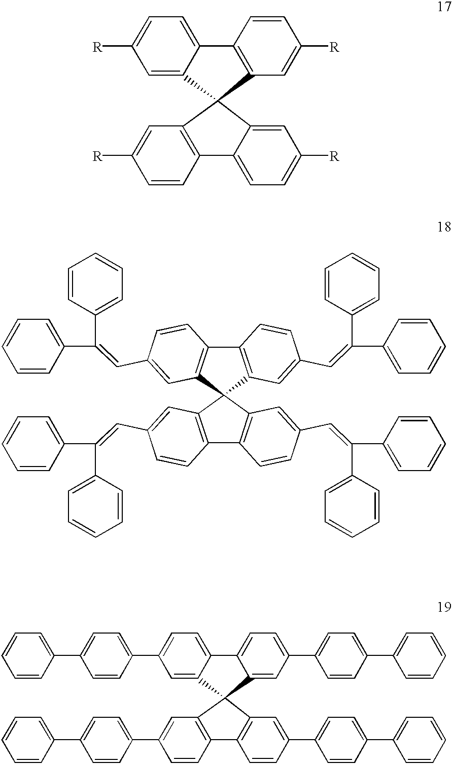
- where each R is independently a conjugated structure having one or more alkenyl, alkenylene, aryl, arylene (e.g., phenylene, naphthylene, or anthrylene), heteroaryl, or heteroarylene functional groups. The substituents can have extended π-conjugated systems which can include heteroatoms such as nitrogen and oxygen. The conjugated systems can include electron rich moieties (e.g. a triarylamine) to stabilize cation radicals (e.g. holes), electron poor moieties to stabilize anion radicals (e.g. electrons), or a HOMO-LUMO (Highest Occupied Molecular Orbital-Lowest Unoccupied Molecular Orbital) gap in the ultraviolet to visible range to act as a chromophore. Again, the polymerizable moieties would be functional groups coupled to the R substituents or phenyl groups of these base structures.
- Other base structures that can be used in polymerizable, amorphous matrix-forming compounds include dendrimers. Dendrimeric structures have a core moiety with three or more dendritic substituents extending from the core moiety. Examples of suitable core moieties include triphenylamine, benzene, pyridine, pyrimidine, and others described in PCT Patent Application Serial No. WO 99/21935, incorporated herein by reference. The dendritic substituents typically contain two or more aryl, arylene (e.g., phenylene), heteroaryl, heteroarylene, alkenyl, or alkenylene substituents. In some embodiments, the substituents can be conjugated structures having one or more alkenyl, alkenylene, aryl, arylene (e.g., phenylene, naphthylene, or anthrylene), heteroaryl, or heteroarylene moieties. The dendritic substituents can be the same or different. Generally, the polymerizable moieties are coupled to the dendritic substituents. Examples of dendrimeric compounds include starburst compounds based on, for example, triphenylamines, such as compounds 20-26:

- Each R 1 and R2 is independently H, F, Cl, Br, I, —SH, —OH, alkyl, aryl, heteroaryl, fluoroalkyl, fluoroalkylalkoxy, alkenyl, alkoxy, amino, or alkyl-COOH. Each R3 is independently H, F, Cl, Br, I, alkyl, fluoroalkyl, alkoxy, aryl, amino, cyano, or nitro. Each X1 is independently O, S, Se, NR3, BR3, or PR3. The alkyl, aryl, and heteroaryl portions of any of these substituents can be substituted or unsubstituted. Each R1, R2, R3, and X1 can be the same as or different from similarly labeled substituents (i.e., all R1 substituents can be the same as or one or more of the R1 substituents can be different from each other).
- Other dendrimer structures can have an aryl or heteroaryl moiety as a core, such as compounds 27-36:

- Each Ar 1 and Ar2 is independently a substituted or unsubstituted aryl or heteroaryl, including, for example, substituted or unsubstituted phenyl, pyridine, pyrole, furan, thiophene, or one of the following structures:

- Each R 1 and R2 is independently H, F, Cl, Br, I, —SH, —OH, alkyl, aryl, heteroaryl, fluoroalkyl, fluoroalkylalkoxy, alkenyl, alkoxy, amino, or alkyl-COOH. Each R3 is independently H, F, Cl, Br, I, alkyl, fluoroalkyl, alkoxy, aryl, amino, cyano, or nitro. Each X1 and X2 is independently O, S, Se, NR3, BR3, or PR3. The alkyl, aryl, and heteroaryl portions of any of these substituents can be substituted or unsubstituted. Each R1, R2, R3, X1, and X2 can be the same as or different from similarly labeled substituents (i.e., all R1 substituents can be the same as or one or more of the R1 substituents can be different from each other).
- Other base structures for the polymerizable, amorphous matrix-forming compounds include, for example, structures 37-42:

- Each Ar 1 and Ar2 is independently a substituted or unsubstituted aryl or heteroaryl, n is an integer in the range of 1 to 6, and each R1 is independently H, F, Cl, Br, I, —SH, —OH, alkyl, aryl, heteroaryl, fluoroalkyl, fluoroalkylalkoxy, alkenyl, alkoxy, amino, or alkyl-COOH. Each R3 is independently H, F, Cl, Br, I, alkyl, fluoroalkyl, alkoxy, aryl, amino, cyano, or nitro. Each X, X1, and X2 are independently O, S, Se, NR3, BR3, or PR3. The alkyl, aryl, and heteroaryl portions of any of these substituents can be substituted or unsubstituted. Each R1, R2, R3, X, X1, and X2 can be the same as or different from similarly labeled substituents (i.e., all R1 substituents can be the same as or one or more of the R1 substituents can be different from each other).
- An optional crosslinker can be included with the polymerizable, amorphous matrix-forming compounds as part of the polymerizable, amorphous matrix-forming material. The crosslinker does not necessarily form an amorphous matrix, but also does not hinder the formation of that amorphous matrix. The crosslinker includes two or more polymerizable moieties that can polymerize with the polymerizable, amorphous matrix-forming compounds. In some embodiments, the crosslinker is necessary to polymerize the polymerizable, amorphous matrix-forming material after transfer to a receptor. Examples of suitable materials include triglycidyl triphenylethane (43), triglycidyl isocyanurate (44), tetramethoxymethyl glycouril (45), tris-1,3,5-(p-trimethoxysilylphenyl)benzene (46), and tris(p-trimethoxysilylpropylphenyl)amine (47).

- For example, an amorphous matrix-forming compound with two or more hydroxyl moieties could be polymerized using tris-1,3,5-(p-trimethoxysilylphenyl)benzene or tris(p-trimethoxysilylpropylphenyl)amine as a crosslinker.
- Unless otherwise indicated, the term “alkyl” includes both straight-chained, branched, and cyclic alkyl groups and includes both unsubstituted and substituted alkyl groups. Unless otherwise indicated, the alkyl groups are typically C1-C20. Examples of “alkyl” as used herein include, but are not limited to, methyl, ethyl, n-propyl, n-butyl, n-pentyl, isobutyl, and isopropyl, and the like.
- Unless otherwise indicated, the term “alkylene” includes both straight-chained, branched, and cyclic divalent hydrocarbon radicals and includes both unsubstituted and substituted alkenylene groups. Unless otherwise indicated, the alkylene groups are typically C1-C20. Examples of “alkylene” as used herein include, but are not limited to, methylene, ethylene, propylene, butylene, and isopropylene, and the like.
- Unless otherwise indicated, the term “alkenyl” includes both straight-chained, branched, and cyclic monovalent hydrocarbon radicals have one or more double bonds and includes both unsubstituted and substituted alkenyl groups. Unless otherwise indicated, the alkenyl groups are typically C2-C20. Examples of “alkenylene” as used herein include, but are not limited to, ethenyl, propenyl, and the like.
- Unless otherwise indicated, the term “alkenylene” includes both straight-chained, branched, and cyclic divalent hydrocarbon radicals have one or more double bonds and includes both unsubstituted and substituted alkenylene groups. Unless otherwise indicated, the alkylene groups are typically C2-C20. Examples of “alkenylene” as used herein include, but are not limited to, ethene-1,2-diyl, propene-1,3-diyl, and the like.
- Unless otherwise indicated, the term “aryl” refers to monovalent unsaturated aromatic carbocyclic radicals having one to fifteen rings, such as phenyl or bipheynyl, or multiple fused rings, such as naphthyl or anthryl, or combinations thereof. Examples of aryl as used herein include, but are not limited to, phenyl, 2-naphthyl, 1-naphthyl, biphenyl, 2-hydroxyphenyl, 2-aminophenyl, 2-methoxyphenyl and the like.
- Unless otherwise indicated, the term “arylene” refers to divalent unsaturated aromatic carbocyclic radicals having one to fifteen rings, such as phenylene, or multiple fused rings, such as naphthylene or anthrylene, or combinations thereof. Examples of “arylene” as used herein include, but are not limited to, benzene-1,2-diyl, benzene-1,3-diyl, benzene-1,4-diyl, naphthalene-1,8-diyl, anthracene-1,4-diyl, and the like.
- Unless otherwise indicated, the term “heteroaryl” refers to functional groups containing a monovalent five—to seven—membered aromatic ring radical with one or more heteroatoms independently selected from S, O, or N. Such a heteroaryl ring may be optionally fused to one or more of another heterocyclic ring(s), heteroaryl ring(s), aryl ring(s), cycloalkenyl ring(s), or cycloalkyl rings. Examples of “heteroaryl” used herein include, but are not limited to, furyl, thiophenyl, pyrrolyl, imidazolyl, pyrazolyl, triazolyl, tetrazolyl, thiazolyl, oxazolyl, isoxazolyl, oxadiazolyl, thiadiazolyl, isothiazolyl, pyridinyl, pyridazinyl, pyrazinyl, pyrimidinyl, quinolinyl, isoquinolinyl, benzofuryl, benzothiophenyl, indolyl, and indazolyl, and the like.
- Unless otherwise indicated, the term “heteroarylene” refers to functional groups containing a divalent five—to seven—membered aromatic ring radical with one or more heteroatoms independently selected from S, O, or N. Such a heteroarylene ring may be optionally fused to one or more of another heterocyclic ring(s), heteroaryl ring(s), aryl ring(s), cycloalkenyl ring(s), or cycloalkyl rings. Examples of “heteroarylene” used herein include, but are not limited to, furan-2,5-diyl, thiophene-2,4-diyl, 1,3,4-oxadiazole-2,5-diyl, 1,3,4-thiadiazole-2,5-diyl, 1,3-thiazole-2,4-diyl, 1,3-thiazole-2,5-diyl, pyridine-2,4-diyl, pyridine-2,3-diyl, pyridine-2,5-diyl, pyrimidine-2,4-diyl, quinoline-2,3-diyl, and the like.
- Suitable substituents for substituted alkyl, alkylene, alkenyl, alkenylene, aryl, arylene, heteroaryl, and heteroarylene groups include, but are not limited to, alkyl, alkylene, alkoxy, aryl, arylene, heteroaryl, heteroarylene, alkenyl, alkenylene, amino, F, Cl, Br, I, —OH, —SH, cyano, nitro, —COOH, and —COO-alkyl.
- Preferably, the polymerizable, amorphous matrix-forming material does not have a substantial propensity to form or does not form a stable, crystalline phase under the expected operating and storage conditions. Preferably, the polymerizable, amorphous matrix-forming material does not have a substantial propensity to polymerize under the expected storage conditions. In addition, preferably, the polymerizable, amorphous matrix-forming material and light emitting material are compatible or soluble in a common solvent or solvents and do not substantially phase separate during solution coating and, more preferably, do not phase separate upon removal of the solvent(s).
- In general, when the amorphous matrix is formed, the threshold for reducing cohesion in an amorphous matrix/LEP (or other light emitting material) blend is the point at which the LEP becomes the discontinuous phase (if there are two observable phases) or the point in which the LEP chains are dissolved by the amorphous matrix (if there is a single phase). Generally, the total amount of light emitting polymer or other light emitting molecule is no more than 50 wt. % of the solids of a coating composition and can be 40wt. %, 25 wt. %, or less of the solids. Typically, the ratio, by weight, of the polymerizable, amorphous matrix-forming material to light emitting material (e.g., light emitting polymer or polymers) is at least 1:1 and typically is in the range of 1:1 to 100:1. Generally, ratios of at least 1: 1, and typically at least 2:1 or 3:1 or more, are suitable for thermal transfer applications.
- In some embodiments, the polymerizable, amorphous matrix-forming material is or includes a hole or electron transport material. In some of these embodiments, a hole or electron transport layer is formed using the polymerizable, amorphous matrix-forming material or a component of that material and coated with or coated onto a light emitting layer containing the same polymerizable, amorphous matrix-forming material.
- In some embodiments, a gradient of light emitting material can be formed by depositing several layers with different concentrations of light emitting material to achieve a desired profile. The thermal transfer methods described below can be useful in creating such structures by sequentially transferring each of the layers. In addition, layers can be formed using different light emitting materials to achieve different colors or to produce, for example, stacked red, green, and blue pixels with intervening electrodes between each pixel.
- If the polymerizable, amorphous matrix-forming material is not a hole or electron transport material, it can be desirable to include a hole or electron transport material as part of the coating composition. Other materials that can be included in the coating composition include, for example, small molecule dopants (e.g. triplet emitters); inert polymers; thermal initiators; photoinitiators; coating aids, surfactants; particulate material to, for example, reduce cohesion; dispersants; stabilizers; and photosensitizers.
- In some embodiments, the polymerizable, amorphous matrix-forming material is also a light emitting molecule. In these embodiments, it is preferred that the materials and operating conditions be selected to favor emission by the light emitting material instead of the polymerizable, amorphous matrix-forming material. For example, the polymerizable, amorphous matrix-forming material may be capable of emitting light in the blue region of the spectrum. In this instance, a light emitting polymer could be selected which emits in the red or green regions of the spectrum. Selection can be based on, for example, the mechanism(s) of molecular energy transfer and the bandgap of the materials. In some instances, the light emitting material or one or more components of the light emitting material includes polymerizable moieties that can polymerize with the polymerizable, amorphous matrix-forming material.
- It will be recognized that electrically active materials other than light emitting materials can be disposed in the amorphous matrix formed using the polymerizable, amorphous matrix-forming material. For example, a conducting or semiconducting material can be disposed in the polymerizable, amorphous matrix-forming material. Application examples include the formation of a hole transport layer or electron transport layer or other charge conducting layer by disposing a hole transport material or electron transport material in the polymerizable, amorphous matrix-forming material. The amorphous matrix can be formed using, for example, any of the materials described above. This structure can be particularly useful for conducting or semiconducting polymeric materials to produce a layer with lower cohesive strength than the polymer itself.
- A variety of light emitting materials including LEP and SM light emitters can be used. The light emitters include, for example, fluorescent and phosphorescent materials. Examples of classes of suitable LEP materials include poly(phenylenevinylene)s (PPVs), poly-para-phenylenes (PPPs), polyfluorenes (PFs), other LEP materials now known or later developed, and co-polymers or blends thereof. Suitable LEPs can also be molecularly doped, dispersed with fluorescent dyes or other PL materials, blended with active or non-active materials, dispersed with active or non-active materials, and the like. Examples of suitable LEP materials are described in Kraft, et al., Angew. Chem. Int. Ed., 37, 402-428 (1998); U.S. Pat. Nos. 5,621,131; 5,708,130; 5,728,801; 5,840,217; 5,869,350; 5,900,327; 5,929,194; 6,132,641; and 6,169,163; and PCT Patent Application Publication No. 99/40655, all of which are incorporated herein by reference.
- SM materials are generally non-polymer organic or organometallic molecular materials that can be used in OEL displays and devices as emitter materials, charge transport materials, as dopants in emitter layers (e.g., to control the emitted color) or charge transport layers, and the like. Commonly used SM materials include metal chelate compounds, such as tris(8-hydroxyquinoline) aluminum (AIQ), and N,N′-bis(3-methylphenyl)-N,N′-diphenylbenzidine (TPD). Other SM materials are disclosed in, for example, C. H. Chen, et al., Macromol. Symp. 125, 1 (1997), Japanese Laid Open Patent Application 2000-195673, U.S. Pat. Nos. 6,030,715, 6,150,043, and 6,242,115 and, PCT Patent Applications Publication Nos. WO 00/18851 (divalent lanthanide metal complexes), WO 00/70655 (cyclometallated iridium compounds and others), and WO 98/55561, all of which are incorporated herein by reference.
- Referring back to FIG. 1,
device layer 110 is disposed onsubstrate 120.Substrate 120 can be any substrate suitable for OEL device and display applications. For example,substrate 120 can comprise glass, clear plastic, or other suitable material(s) that are substantially transparent to visible light.Substrate 120 can also be opaque to visible light, for example stainless steel, crystalline silicon, poly-silicon, or the like. Because some materials in OEL devices can be particularly susceptible to damage due to exposure to oxygen or water,substrate 120 preferably provides an adequate environmental barrier, or is supplied with one or more layers, coatings, or laminates that provide an adequate environmental barrier. -
Substrate 120 can also include any number of devices or components suitable in OEL devices and displays such as transistor arrays and other electronic devices; color filters, polarizers, wave plates, diffusers, and other optical devices; insulators, barrier ribs, black matrix, mask work and other such components; and the like. Generally, one or more electrodes will be coated, deposited, patterned, or otherwise disposed onsubstrate 120 before forming the remaining layer or layers of the OEL device or devices of thedevice layer 110. When alight transmissive substrate 120 is used and the OEL device or devices are bottom emitting, the electrode or electrodes that are disposed between thesubstrate 120 and the emissive material(s) are preferably substantially transparent to light, for example transparent conductive electrodes such as indium tin oxide (ITO) or any of a number of other transparent conductive oxides. -
Element 130 can be any element or combination of elements suitable for use with OEL display ordevice 100. For example,element 130 can be an LCD module whendevice 100 is a backlight. One or more polarizers or other elements can be provided between the LCD module and thebacklight device 100, for instance an absorbing or reflective clean-up polarizer. Alternatively, whendevice 100 is itself an information display,element 130 can include one or more of polarizers, wave plates, touch panels, antireflective coatings, anti-smudge coatings, projection screens, brightness enhancement films, or other optical components, coatings, user interface devices, or the like. - Organic electronic devices containing materials for light emission can be made at least in part by selective thermal transfer of light emitting material from a thermal transfer donor sheet to a desired receptor substrate. For example, light emitting polymer displays and lamps can be made coating an LEP and a polymerizable, amorphous matrix-forming material on a donor sheet and then selectively transferring the LEP layer alone or along with other device layers or materials to the display substrate.
- Selective thermal transfer of layers containing light emitting materials for organic electronic devices can be performed using a thermal transfer donor. FIG. 2 shows an example of a
thermal transfer donor 200 suitable for use in the present invention.Donor element 200 includes abase substrate 210, anoptional underlayer 212, an optional light-to-heat conversion layer (LTHC layer) 214, anoptional interlayer 216, and atransfer layer 218. Each of these elements are described in more detail in the discussion that follows. Other layers can also be present. Examples of suitable donors or layers of donors are disclosed in U.S. Pat. Nos. 6,242,152; 6,228,555; 6,228,543; 6,221,553; 6,221,543; 6,214,520; 6,194,119; 6,114,088; 5,998,085; 5,725,989; 5,710,097; 5,695,907; and 5,693,446, and in co-assigned U.S. patent application Ser. Nos. 09/853,062; 09/844,695; 09/844,100; 09/662,980; 09/662,845; 09/473,114; 09/451,984; 09/931,598; 10/004,706; and 10/183,717, all of which are incorporated herein by reference. - In processes of the present invention, emissive organic materials, including LEPs or other materials, can be selectively transferred from the transfer layer of a donor sheet to a receptor substrate by placing the transfer layer of the donor element adjacent to the receptor and selectively heating the donor element. Illustratively, the donor element can be selectively heated by irradiating the donor element with imaging radiation that can be absorbed by light-to-heat converter material disposed in the donor, often in a separate LTHC layer, and converted into heat. In these cases, the donor can be exposed to imaging radiation through the donor substrate, through the receptor, or both. The radiation can include one or more wavelengths, including visible light, infrared radiation, or ultraviolet radiation, for example from a laser, lamp, or other such radiation source. Other selective heating methods can also be used, such as using a thermal print head or using a thermal hot stamp (e.g., a patterned thermal hot stamp such as a heated silicone stamp that has a relief pattern that can be used to selectively heat a donor). Material from the thermal transfer layer can be selectively transferred to a receptor in this manner to imagewise form patterns of the transferred material on the receptor. In many instances, thermal transfer using light from, for example, a lamp or laser, to patternwise expose the donor can be advantageous because of the accuracy and precision that can often be achieved. The size and shape of the transferred pattern (e.g., a line, circle, square, or other shape) can be controlled by, for example, selecting the size of the light beam, the exposure pattern of the light beam, the duration of directed beam contact with the donor sheet, or the materials of the donor sheet. The transferred pattern can also be controlled by irradiating the donor element through a mask.
- As mentioned, a thermal print head or other heating element (patterned or otherwise) can also be used to selectively heat the donor element directly, thereby pattern-wise transferring portions of the transfer layer. In such cases, the light-to-heat converter material in the donor sheet is optional. Thermal print heads or other heating elements may be particularly suited for making lower resolution patterns of material or for patterning elements whose placement need not be precisely controlled.
- Transfer layers can also be transferred from donor sheets without selectively transferring the transfer layer. For example, a transfer layer can be formed on a donor substrate that, in essence, acts as a temporary liner that can be released after the transfer layer is contacted to a receptor substrate, typically with the application of heat or pressure. Such a method, referred to as lamination transfer, can be used to transfer the entire transfer layer, or a large portion thereof, to the receptor.
- The mode of thermal mass transfer can vary depending on the type of selective heating employed, the type of irradiation if used to expose the donor, the type of materials and properties of the optional LTHC layer, the type of materials in the transfer layer, the overall construction of the donor, the type of receptor substrate, and the like. Without wishing to be bound by any theory, transfer generally occurs via one or more mechanisms, one or more of which may be emphasized or de-emphasized during selective transfer depending on imaging conditions, donor constructions, and so forth. One mechanism of thermal transfer includes thermal melt-stick transfer whereby localized heating at the interface between the thermal transfer layer and the rest of the donor element can lower the adhesion of the thermal transfer layer to the donor in selected locations. Selected portions of the thermal transfer layer can adhere to the receptor more strongly than to the donor so that when the donor element is removed, the selected portions of the transfer layer remain on the receptor. Another mechanism of thermal transfer includes ablative transfer whereby localized heating can be used to ablate portions of the transfer layer off of the donor element, thereby directing ablated material toward the receptor. Yet another mechanism of thermal transfer includes sublimation whereby material dispersed in the transfer layer can be sublimated by heat generated in the donor element. A portion of the sublimated material can condense on the receptor. The present invention contemplates transfer modes that include one or more of these and other mechanisms whereby selective heating of a donor sheet can be used to cause the transfer of materials from a transfer layer to receptor surface.
- A variety of radiation-emitting sources can be used to heat donor sheets. For analog techniques (e.g., exposure through a mask), high-powered light sources (e.g., xenon flash lamps and lasers) are useful. For digital imaging techniques, infrared, visible, and ultraviolet lasers are particularly useful. Suitable lasers include, for example, high power (≧100 mW) single mode laser diodes, fiber-coupled laser diodes, and diode-pumped solid state lasers (e.g., Nd:YAG and Nd:YLF). Laser exposure dwell times can vary widely from, for example, a few hundredths of microseconds to tens of microseconds or more, and laser fluences can be in the range from, for example, about 0.01 to about 5 J/cm 2 or more. Other radiation sources and irradiation conditions can be suitable based on, among other things, the donor element construction, the transfer layer material, the mode of thermal mass transfer, and other such factors.
- When high spot placement accuracy is desired (e.g., when patterning elements for high information content displays and other such applications) over large substrate areas, a laser can be particularly useful as the radiation source. Laser sources are also compatible with both large rigid substrates (e.g., 1 m×1 m×1.1 mm glass) and continuous or sheeted film substrates (e.g., 100 μm thick polyimide sheets).
- During imaging, the donor sheet can be brought into intimate contact with a receptor (as might typically be the case for thermal melt-stick transfer mechanisms) or the donor sheet can be spaced some distance from the receptor (as can be the case for ablative transfer mechanisms or material sublimation transfer mechanisms). In at least some instances, pressure or vacuum can be used to hold the donor sheet in intimate contact with the receptor. In some instances, a mask can be placed between the donor sheet and the receptor. Such a mask can be removable or can remain on the receptor after transfer. If a light-to-heat converter material is present in the donor, radiation source can then be used to heat the LTHC layer (or other layer(s) containing radiation absorber) in an imagewise fashion (e.g., digitally or by analog exposure through a mask) to perform imagewise transfer or patterning of the transfer layer from the donor sheet to the receptor.
- Typically, selected portions of the transfer layer are transferred to the receptor without transferring significant portions of the other layers of the donor sheet, such as the optional interlayer or LTHC layer. The presence of the optional interlayer may eliminate or reduce the transfer of material from an LTHC layer to the receptor or reduce distortion in the transferred portion of the transfer layer. Preferably, under imaging conditions, the adhesion of the optional interlayer to the LTHC layer is greater than the adhesion of the interlayer to the transfer layer. The interlayer can be transmissive, reflective, or absorptive to imaging radiation, and can be used to attenuate or otherwise control the level of imaging radiation transmitted through the donor or to manage temperatures in the donor, for example to reduce thermal or radiation-based damage to the transfer layer during imaging. Multiple interlayers can be present.
- Large donor sheets can be used, including donor sheets that have length and width dimensions of a meter or more. In operation, a laser can be rastered or otherwise moved across the large donor sheet, the laser being selectively operated to illuminate portions of the donor sheet according to a desired pattern. Alternatively, the laser may be stationary and the donor sheet or receptor substrate moved beneath the laser.
- In some instances, it may be necessary, desirable, or convenient to sequentially use two or more different donor sheets to form electronic devices on a receptor. For example, multiple layer devices can be formed by transferring separate layers or separate stacks of layers from different donor sheets. Multilayer stacks can also be transferred as a single transfer unit from a single donor element. For example, a hole transport layer and a LEP layer can be co-transferred from a single donor. As another example, a semiconductive polymer and an emissive layer can be co-transferred from a single donor. Multiple donor sheets can also be used to form separate components in the same layer on the receptor. For example, three different donors that each have a transfer layer comprising a LEP capable of emitting a different color (for example, red, green, and blue) can be used to form RGB sub-pixel OEL devices for a full color polarized light emitting electronic display. As another example, a conductive or semiconductive polymer can be patterned via thermal transfer from one donor, followed by selective thermal transfer of emissive layers from one or more other donors to form a plurality of OEL devices in a display. As still another example, layers for organic transistors can be patterned by selective thermal transfer of electrically active organic materials (oriented or not), followed by selective thermal transfer patterning of one or more pixel or sub-pixel elements such as color filters, emissive layers, charge transport layers, electrode layers, and the like.
- Materials from separate donor sheets can be transferred adjacent to other materials on a receptor to form adjacent devices, portions of adjacent devices, or different portions of the same device. Alternatively, materials from separate donor sheets can be transferred directly on top of, or in partial overlying registration with, other layers or materials previously patterned onto the receptor by thermal transfer or some other method (e.g., photolithography, deposition through a shadow mask, etc.). A variety of other combinations of two or more donor sheets can be used to form a device, each donor sheet forming one or more portions of the device. It will be understood that other portions of these devices, or other devices on the receptor, may be formed in whole or in part by any suitable process including photolithographic processes, ink jet processes, and various other printing or mask-based processes, whether conventionally used or newly developed.
- Referring back to FIG. 2, various layers of the
donor sheet 200 will now be described. - The
donor substrate 210 can be a polymer film. One suitable type of polymer film is a polyester film, for example, polyethylene terephthalate (PET) or polyethylene naphthalate (PEN) films. However, other films with sufficient optical properties, including high transmission of light at a particular wavelength, or sufficient mechanical and thermal stability properties, depending on the particular application, can be used. The donor substrate, in at least some instances, is flat so that uniform coatings can be formed thereon. The donor substrate is also typically selected from materials that remain stable despite heating of one or more layers of the donor. However, as described below, the inclusion of an underlayer between the substrate and an LTHC layer can be used to insulate the substrate from heat generated in the LTHC layer during imaging. The typical thickness of the donor substrate ranges from 0.025 to 0.15 mm, preferably 0.05 to 0.1 mm, although thicker or thinner donor substrates may be used. - The materials used to form the donor substrate and an optional adjacent underlayer can be selected to improve adhesion between the donor substrate and the underlayer, to control heat transport between the substrate and the underlayer, to control imaging radiation transport to the LTHC layer, to reduce imaging defects and the like. An optional priming layer can be used to increase uniformity during the coating of subsequent layers onto the substrate and also increase the bonding strength between the donor substrate and adjacent layers.
- An
optional underlayer 212 may be coated or otherwise disposed between a donor substrate and the LTHC layer, for example to control heat flow between the substrate and the LTHC layer during imaging or to provide mechanical stability to the donor element for storage, handling, donor processing, or imaging. Examples of suitable underlayers and methods of providing underlayers are disclosed in co-assigned U.S. patent application Ser. No. 09/743,114, incorporated herein by reference. - The underlayer can include materials that impart desired mechanical or thermal properties to the donor element. For example, the underlayer can include materials that exhibit a low product of specific heat and density (e.g., specific heat×density) or low thermal conductivity relative to the donor substrate. Such an underlayer may be used to increase heat flow to the transfer layer, for example to improve the imaging sensitivity of the donor.
- The underlayer may also include materials for their mechanical properties or for adhesion between the substrate and the LTHC. Using an underlayer that improves adhesion between the substrate and the LTHC layer may result in less distortion in the transferred image. As an example, in some cases an underlayer can be used that reduces or eliminates delamination or separation of the LTHC layer, for example, that might otherwise occur during imaging of the donor media. This can reduce the amount of physical distortion exhibited by transferred portions of the transfer layer. In other cases, however it may be desirable to employ underlayers that promote at least some degree of separation between or among layers during imaging, for example to produce an air gap between layers during imaging that can provide a thermal insulating function. Separation during imaging may also provide a channel for the release of gases that may be generated by heating of the LTHC layer during imaging. Providing such a channel may lead to fewer imaging defects.
- The underlayer may be substantially transparent at the imaging wavelength, or may also be at least partially absorptive or reflective of imaging radiation. Attenuation or reflection of imaging radiation by the underlayer may be used to control heat generation during imaging.
- Referring again to FIG. 2, an
LTHC layer 214 can be included in donor sheets of the present invention to couple irradiation energy into the donor sheet. The LTHC layer preferably includes a radiation absorber that absorbs incident radiation (e.g., laser light) and converts at least a portion of the incident radiation into heat to enable transfer of the transfer layer from the donor sheet to the receptor. - Generally, the radiation absorber(s) in the LTHC layer absorb light in the infrared, visible, or ultraviolet regions of the electromagnetic spectrum and convert the absorbed radiation into heat. The radiation absorber(s) are typically highly absorptive of the selected imaging radiation, providing an LTHC layer with an optical density at the wavelength of the imaging radiation in the range of about 0.2 to 3 or higher. Optical density of a layer is the absolute value of the logarithm (base 10) of the ratio of the intensity of light transmitted through the layer to the intensity of light incident on the layer.
- Radiation absorber material can be uniformly disposed throughout the LTHC layer or can be non-homogeneously distributed. For example, as described in co-assigned U.S. patent application Ser. No. 09/474,002, non-homogeneous LTHC layers can be used to control temperature profiles in donor elements. This can give rise to donor sheets that have improved transfer properties (e.g., better fidelity between the intended transfer patterns and actual transfer patterns).
- Suitable radiation absorbing materials can include, for example, dyes (e.g., visible dyes, ultraviolet dyes, infrared dyes, fluorescent dyes, and radiation-polarizing dyes), pigments, metals, metal compounds, metal films, and other suitable absorbing materials. Examples of suitable radiation absorbers includes carbon black, metal oxides, and metal sulfides. One example of a suitable LTHC layer can include a pigment, such as carbon black, and a binder, such as an organic polymer. Another suitable LTHC layer includes metal or metal/metal oxide formed as a thin film, for example, black aluminum (i.e., a partially oxidized aluminum having a black visual appearance). Metallic and metal compound films may be formed by techniques, such as, for example, sputtering and evaporative deposition. Particulate coatings may be formed using a binder and any suitable dry or wet coating techniques. LTHC layers can also be formed by combining two or more LTHC layers containing similar or dissimilar materials. For example, an LTHC layer can be formed by vapor depositing a thin layer of black aluminum over a coating that contains carbon black disposed in a binder.
- Dyes suitable for use as radiation absorbers in a LTHC layer may be present in particulate form, dissolved in a binder material, or at least partially dispersed in a binder material. When dispersed particulate radiation absorbers are used, the particle size can be, at least in some instances, about 10 μm or less, and may be about 1 μm or less. Suitable dyes include those dyes that absorb in the IR region of the spectrum. A specific dye may be chosen based on factors such as, solubility in, and compatibility with, a specific binder or coating solvent, as well as the wavelength range of absorption.
- Pigmentary materials may also be used in the LTHC layer as radiation absorbers. Examples of suitable pigments include carbon black and graphite, as well as phthalocyanines, nickel dithiolenes, and other pigments described in U.S. Pat. Nos. 5,166,024 and 5,351,617. Additionally, black azo pigments based on copper or chromium complexes of, for example, pyrazolone yellow, dianisidine red, and nickel azo yellow can be useful. Inorganic pigments can also be used, including, for example, oxides and sulfides of metals such as aluminum, bismuth, tin, indium, zinc, titanium, chromium, molybdenum, tungsten, cobalt, iridium, nickel, palladium, platinum, copper, silver, gold, zirconium, iron, lead, and tellurium. Metal borides, carbides, nitrides, carbonitrides, bronze-structured oxides, and oxides structurally related to the bronze family (e.g., WO 2.9) may also be used.
- Metal radiation absorbers may be used, either in the form of particles, as described for instance in U.S. Pat. No. 4,252,671, or as films, as disclosed in U.S. Pat. No. 5,256,506. Suitable metals include, for example, aluminum, bismuth, tin, indium, tellurium and zinc.
- Suitable binders for use in the LTHC layer include film-forming polymers, such as, for example, phenolic resins (e.g., novolak and resole resins), polyvinyl butyral resins, polyvinyl acetates, polyvinyl acetals, polyvinylidene chlorides, polyacrylates, cellulosic ethers and esters, nitrocelluloses, and polycarbonates. Suitable binders may include monomers, oligomers, or polymers that have been, or can be, polymerized or crosslinked. Additives such as photoinitiators may also be included to facilitate crosslinking of the LTHC binder. In some embodiments, the binder is primarily formed using a coating of crosslinkable monomers or oligomers with optional polymer.
- The inclusion of a thermoplastic resin (e.g., polymer) may improve, in at least some instances, the performance (e.g., transfer properties or coatability) of the LTHC layer. It is thought that a thermoplastic resin may improve the adhesion of the LTHC layer to the donor substrate. In one embodiment, the binder includes 25 to 50 wt. % (excluding the solvent when calculating weight percent) thermoplastic resin, and, preferably, 30 to 45 wt. % thermoplastic resin, although lower amounts of thermoplastic resin may be used (e.g., 1 to 15 wt. %). The thermoplastic resin is typically chosen to be compatible (i.e., form a one-phase combination) with the other materials of the binder. In at least some embodiments, a thermoplastic resin that has a solubility parameter in the range of 9 to 13 (cal/cm 3)½, preferably, 9.5 to 12 (cal/cm3)½, is chosen for the binder. Examples of suitable thermoplastic resins include polyacrylics, styrene-acrylic polymers and resins, and polyvinyl butyral.
- Conventional coating aids, such as surfactants and dispersing agents, may be added to facilitate the coating process. The LTHC layer may be coated onto the donor substrate using a variety of coating methods known in the art. A polymeric or organic LTHC layer can be coated, in at least some instances, to a thickness of 0.05 μm to 20 μm, preferably, 0.5 μm to 10 μm, and, more preferably, 1 μm to 7 μm. An inorganic LTHC layer can be coated, in at least some instances, to a thickness in the range of 0.0005 to 10 μm, and preferably, 0.001 to 1 μm.
- Referring again to FIG. 2, an
optional interlayer 216 may be disposed between theLTHC layer 214 andtransfer layer 218. The interlayer can be used, for example, to minimize damage and contamination of the transferred portion of the transfer layer and may also reduce distortion in the transferred portion of the transfer layer. The interlayer may also influence the adhesion of the transfer layer to the rest of the donor sheet. Typically, the interlayer has high thermal resistance. Preferably, the interlayer does not distort or chemically decompose under the imaging conditions, particularly to an extent that renders the transferred image non-functional. The interlayer typically remains in contact with the LTHC layer during the transfer process and is not substantially transferred with the transfer layer. - Suitable interlayers include, for example, polymer films, metal layers (e.g., vapor deposited metal layers), inorganic layers (e.g., sol-gel deposited layers and vapor deposited layers of inorganic oxides (e.g., silica, titania, and other metal oxides)), and organic/inorganic composite layers. Organic materials suitable as interlayer materials include both thermoset and thermoplastic materials. Suitable thermoset materials include resins that may be crosslinked by heat, radiation, or chemical treatment including, but not limited to, crosslinked or crosslinkable polyacrylates, polymethacrylates, polyesters, epoxies, and polyurethanes. The thermoset materials may be coated onto the LTHC layer as, for example, thermoplastic precursors and subsequently crosslinked to form a crosslinked interlayer.
- Suitable thermoplastic materials include, for example, polyacrylates, polymethacrylates, polystyrenes, polyurethanes, polysulfones, polyesters, and polyimides. These thermoplastic organic materials may be applied via conventional coating techniques (for example, solvent coating, spray coating, or extrusion coating). Typically, the glass transition temperature (T g) of thermoplastic materials suitable for use in the interlayer is 25° C. or greater, preferably 50° C. or greater. In some embodiments, the interlayer includes a thermoplastic material that has a Tg greater than any temperature attained in the transfer layer during imaging. The interlayer may be either transmissive, absorbing, reflective, or some combination thereof, at the imaging radiation wavelength.
- Inorganic materials suitable as interlayer materials include, for example, metals, metal oxides, metal sulfides, and inorganic carbon coatings, including those materials that are highly transmissive or reflective at the imaging light wavelength. These materials may be applied to the light-to-heat-conversion layer via conventional techniques (e.g., vacuum sputtering, vacuum evaporation, or plasma jet deposition).
- The interlayer may provide a number of benefits. The interlayer may be a barrier against the transfer of material from the light-to-heat conversion layer. It may also modulate the temperature attained in the transfer layer so that thermally unstable materials can be transferred. For example, the interlayer can act as a thermal diffuser to control the temperature at the interface between the interlayer and the transfer layer relative to the temperature attained in the LTHC layer. This may improve the quality (i.e., surface roughness, edge roughness, etc.) of the transferred layer. The presence of an interlayer may also result in improved plastic memory in the transferred material.
- The interlayer may contain additives, including, for example, photoinitiators, surfactants, pigments, plasticizers, and coating aids. The thickness of the interlayer may depend on factors such as, for example, the material of the interlayer, the material and properties of the LTHC layer, the material and properties of the transfer layer, the wavelength of the imaging radiation, and the duration of exposure of the donor sheet to imaging radiation. For polymer interlayers, the thickness of the interlayer typically is in the range of 0.05 μm to 10 μm. For inorganic interlayers (e.g., metal or metal compound interlayers), the thickness of the interlayer typically is in the range of 0.005 μm to 10 μm.
- Referring again to FIG. 2, a
thermal transfer layer 218 is included indonor sheet 200.Transfer layer 218 can include any suitable material or materials, disposed in one or more layers, alone or in combination with other materials.Transfer layer 218 is capable of being selectively transferred as a unit or in portions by any suitable transfer mechanism when the donor element is exposed to direct heating or to imaging radiation that can be absorbed by light-to-heat converter material and converted into heat. - The present invention contemplates a transfer layer that includes a light emitting, charge transporting, charge blocking, or semiconducting material disposed in a polymerizable, amorphous matrix-forming material that forms an amorphous matrix as part of the transfer layer. The present invention contemplates a transfer layer that includes a LEP or other light emitting molecules as the light emitting material. One way of providing the transfer layer is by solution coating the light emitting material and polymerizable, amorphous matrix-forming material onto the donor to form an amorphous matrix containing the light emitting material. In this method, the light emitting material and the polymerizable, amorphous matrix-forming material can be solubilized by addition of a suitable compatible solvent, and coated onto the donor sheet by spin-coating, gravure coating, mayer rod coating, knife coating and the like. The solvent chosen preferably does not undesirably interact with (e.g., swell or dissolve) any of the already existing layers in the donor sheet. The coating can then be optionally annealed and the solvent evaporated to leave a transfer layer containing an amorphous matrix.
- The transfer layer can then be selectively thermally transferred from the donor element to a proximately located receptor substrate. There can be, if desired, more than one transfer layer so that a multilayer construction is transferred using a single donor sheet. The additional transfer layers can include a polymerizable, amorphous matrix-forming material or some other materials. The receptor substrate may be any item suitable for a particular application including, but not limited to, glass, transparent films, reflective films, metals, semiconductors, and plastics. For example, receptor substrates may be any type of substrate or display element suitable for display applications. Receptor substrates suitable for use in displays such as liquid crystal displays or emissive displays include rigid or flexible substrates that are substantially transmissive to visible light. Examples of suitable rigid receptors include glass and rigid plastic that are coated or patterned with indium tin oxide or are circuitized with low temperature poly-silicon (LTPS) or other transistor structures, including organic transistors.
- Suitable flexible substrates include substantially clear and transmissive polymer films, reflective films, transflective films, polarizing films, multilayer optical films, and the like. Flexible substrates can also be coated or patterned with electrode materials or transistors, for example transistor arrays formed directly on the flexible substrate or transferred to the flexible substrate after being formed on a temporary carrier substrate. Suitable polymer substrates include polyester base (e.g., polyethylene terephthalate, polyethylene naphthalate), polycarbonate resins, polyolefin resins, polyvinyl resins (e.g., polyvinyl chloride, polyvinylidene chloride, polyvinyl acetals, etc.), cellulose ester bases (e.g., cellulose triacetate, cellulose acetate), and other conventional polymeric films used as supports. For making OELs on plastic substrates, it is often desirable to include a barrier film or coating on one or both surfaces of the plastic substrate to protect the organic light emitting devices and their electrodes from exposure to undesired levels of water, oxygen, and the like.
- Receptor substrates can be pre-patterned with any one or more of electrodes, transistors, capacitors, insulator ribs, spacers, color filters, black matrix, hole transport layers, electron transport layers, and other elements useful for electronic displays or other devices.
- The present invention contemplates polarized light emitting OEL displays and devices. In one embodiment, OEL displays can be made that emit light and that have adjacent devices that can emit light having different color. For example, FIG. 3 shows an
OEL display 300 that includes a plurality ofOEL devices 310 disposed on asubstrate 320.Adjacent devices 310 can be made to emit different colors of light. - The separation shown between
devices 310 is for illustrative purposes only. Adjacent devices may be separated, in contact, overlapping, etc., or different combinations of these in more than one direction on the display substrate. For example, a pattern of parallel striped transparent conductive anodes can be formed on the substrate followed by a striped pattern of a hole transport material and a striped repeating pattern of red, green, and blue light emitting LEP layers, followed by a striped pattern of cathodes, the cathode stripes oriented perpendicular to the anode stripes. Such a construction may be suitable for forming passive matrix displays. In other embodiments, transparent conductive anode pads can be provided in a two-dimensional pattern on the substrate and associated with addressing electronics such as one or more transistors, capacitors, etc., such as are suitable for making active matrix displays. Other layers, including the light emitting layer(s) can then be coated or deposited as a single layer or can be patterned (e.g., parallel stripes, two-dimensional pattern commensurate with the anodes, etc.) over the anodes or electronic devices. Any other suitable construction is also contemplated by the present invention. - In one embodiment,
display 300 can be a multiple color display. As such, it may be desirable to position optional polarizer 330 between the light emitting devices and a viewer, for example to enhance the contrast of the display. In exemplary embodiments, each of thedevices 310 emits light. There are many displays and devices constructions covered by the general construction illustrated in FIG. 3. Some of those constructions are discussed as follows. - OEL backlights can include emissive layers. Constructions can include bare or circuitized substrates, anodes, cathodes, hole transport layers, electron transport layers, hole-injection layers, electron injection layers, emissive layers, color changing layers, and other layers and materials suitable in OEL devices. Constructions can also include polarizers, diffusers, light guides, lenses, light control films, brightness enhancement films, and the like. Applications include white or single color large area single pixel lamps, for example where an emissive material is provided by thermal stamp transfer, lamination transfer, resistive head thermal printing, or the like; white or single color large area single electrode pair lamps that have a large number of closely spaced emissive layers patterned by laser induced thermal transfer; and tunable color multiple electrode large area lamps.
- Low resolution OEL displays can include emissive layers. Constructions can include bare or circuitized substrates, anodes, cathodes, hole transport layers, electron transport layers, hole injection layers, electron injection layers, emissive layers, color changing layers, and other layers and materials suitable in OEL devices. Constructions can also include polarizers, diffusers, light guides, lenses, light control films, brightness enhancement films, and the like. Applications include graphic indicator lamps (e.g., icons); segmented alphanumeric displays (e.g., appliance time indicators); small monochrome passive or active matrix displays; small monochrome passive or active matrix displays plus graphic indicator lamps as part of an integrated display (e.g., cell phone displays); large area pixel display tiles (e.g., a plurality of modules, or tiles, each having a relatively small number of pixels), such as may be suitable for, outdoor display used; and security display applications.
- High resolution OEL displays can include emissive layers. Constructions can include bare or circuitized substrates, anodes, cathodes, hole transport layers, electron transport layers, hole injection layers, electron injection layers, emissive layers, color changing layers, and other layers and materials suitable in OEL devices. Constructions can also include polarizers, diffusers, light guides, lenses, light control films, brightness enhancement films, and the like. Applications include active or passive matrix multicolor or full color displays; active or passive matrix multicolor or full color displays plus segmented or graphic indicator lamps (e.g., laser induced transfer of high resolution devices plus thermal hot stamp of icons on the same substrate); and security display applications.
-

- 1-(7-Methoxy-fluoren-2-yl)-ethanone is prepared by the acylation of fluoren-2-yl-methyl ether with acetyl chloride/AlCl 3 according to Kajigaeshi, et al., Bull. Chem. Soc. Jpn., 52, 3569-3572 (1979) or Gray et al, J. Chem Soc., 1955; 2686-2688, both of which are incorporated herein by reference.
-

- 1-(7-bromo-9H-fluoren-2-yl)-ethanone is prepared by the reaction of 2-bromofluorene (available from Aldrich Chemical Company, Milwaukee, Wis.) with acetic anhydride/AlCl 3/nitrobenzene according to Tsuno et al., Bull. Chem. Soc. Jpn., 51, 601-607 (1978), incorporated herein by reference.
-

- Benzyltriethylammonium chloride (3.19 g, 14 mmole, 0.077 eq) and 1-(7-bromo-9H-fluoren-2-yl)-ethanone (52.26 g, 182 mmole, 1 eq) are suspended in 178 mL DMSO. 50% aqueous NaOH (80 mL) is added. 1-Bromopropane (59.88 g, 437 mmole, 2.4 eq) is then added in small portions. The reaction is stirred at room temperature for 2 hours before it is stopped and the aqueous layer is then extracted with ether. The combined ether layers are washed with water five times and dried over Na 2SO4. The organic layer is then filtered, evaporated to dryness and the residue flash chromatographed on a silica-gel column to give 1-(7-bromo-9,9-dipropyl-9H-fluoren-2-yl)-ethanone.
-
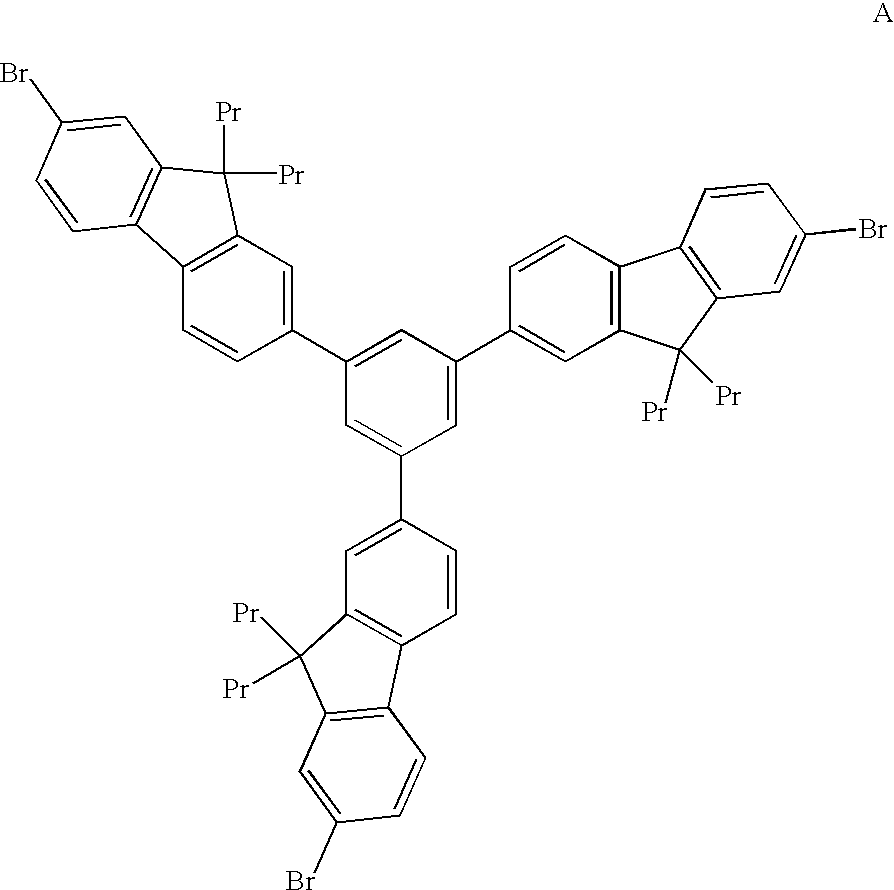
- A mixture of 1-(7-bromo-9,9-dipropyl-9H-fluoren-2-yl)-ethanone from Example 3 (20 g, 53.9 mmol) in 150 mL p-cymene and p-MeC 6H4SO3H (0.3 g) is refluxed for 3 days in a Dean Stark apparatus to give compound A.
-

- Compound 1 can be synthesized by a method similar to that described in W. A. Nugent and R. J. MckKinney, J. Org. Chem., 50, 5370-5372 (1985), incorporated herein by reference. Tribromide A of Example 4 (1 mmole) and [bis(dimethylphosphino)ethane]nickel (II) chloride (0.03 mmol) in THF are treated with vinylmagnesium bromide (3.75 mL, 1.0 M solution in THF) at room temperature. After the reaction is completed, it is quenched with half-saturated aqueous NH4Cl solution. The mixture is extracted with ether and the product is obtained after evaporation of the ether.
- An azide compound can be synthesized by a method similar to that described in P. A. S. Smith, C. D. Rowe and L. B. Bruner, J. Org. Chem., 34, 3430-3433 (1969), incorporated herein by reference. Tribromide A of Example 4 (1 mmole) in ether (10 mL) is treated with magnesium turning (4 mmole) at gentle reflux. After the reaction is completed, the reaction mixture is added to a solution of p-toluene sulfonyl azide (3.3 mmole) in 10 mL of ether at 0° C. Upon completion of the addition, tetrasodium pyrophosphate decahydrate (3 mmol) in water is added dropwise. After stirring overnight, the ether layer is separated, dried over CaCl 2 and purified by eluting on alumina column with petroleum ether. Evaporation of the petroleum ether gives the product.
-

- Tribromide A of Example 4 (30.0 mmol) is dissolved in diethylamine (250 ml) under an atmosphere of argon. Copper iodide (50 mg) and dichlorobis(triphenylphosphine)palladium (II) (400 mg) are added to the stirred solution. Trimethylsilylacetylene (10.6 g, 108 mmol) is added and the mixture heated at 50° C. for 7 h. After cooling, the formed precipitate of diethylamine bromide hydrobromide is filtered off and washed with ether. The combined filtrates are then evaporated to dryness and the residue is then chromatographed on a column (Al 2O3 support, light petroleum ether). The result is treated with a mixture of MeOH—NaOH (50 ml; 30 ml 1M) under stirring at room temperature for 1 h. The organic solvent is evaporated and the residue is extracted with ether and dried (Na2SO4). Removal of solvent gives the product which can be purified by sublimation.
-

- This compound is made by the same general method as the preparation of the tribromide A of Example 4 except that 1-(7-Methoxy-fluoren-2-yl)-ethanone (from Example 1) is used instead of 1-(7-bromo-9,9-dipropyl-9H-fluoren-2-yl)-ethanone.
-

- This alcohol can be synthesized by demethylation of the compound of Example 8 under standard conditions using BBr 3.
- Alternatively, this alcohol can be synthesized by a method similar to that described in M. F. Hawthorne, J. Org. Chem., 22, 1001 (1957), incorporated herein by reference. Tribromide A of Example 4 (1 mmole) in ether (10 mL) is treated with magnesium turning (4 mmole) at gentle reflux. After the reaction is completed, it is added to a solution of methyl borate (3.3 mmole) in 10 mL of ether at −78° C. Upon completion of the addition, the reaction is allowed to warm up to room temperature while 3 mL of 10% HCl is added. The ether layer is separated and washed with water several times. 3 mL of 10% H 2O2 is then added to the ether layer. The ether layer is then washed with (NH4)2Fe(SO4)2 aqueous solution to remove the excess H2O2. Evaporation of the ether gives the product.
- This compound can be synthesized from tribromide A of Example 4 by a method similar to that described in Example 1 of U.S. Pat. No. 5,023,380, incorporated herein by reference.
- This methacrylate compound can be synthesized from the alcohol of Example 9 by reacting the alcohol with methacryloyl chloride under typical acylation conditions.
- The present invention should not be considered limited to the particular examples described above, but rather should be understood to cover all aspects of the invention as fairly set out in the attached claims. Various modifications, equivalent processes, as well as numerous structures to which the present invention may be applicable will be readily apparent to those of skill in the art to which the present invention is directed upon review of the instant specification.
- Each of the patents, patent documents, and publications cited above is hereby incorporated into this document as if reproduced in full.
Claims (24)


Priority Applications (12)
| Application Number | Priority Date | Filing Date | Title |
|---|---|---|---|
| US10/208,910 US7445825B2 (en) | 2001-08-16 | 2002-07-30 | Donor sheet having a polymerizable, amorphous matrix with electrically active material disposed therein |
| JP2003521064A JP2005500653A (en) | 2001-08-16 | 2002-08-15 | Method and material for patterning polymerizable amorphous matrix with electroactive material disposed therein |
| PCT/US2002/026043 WO2003017732A1 (en) | 2001-08-16 | 2002-08-15 | Method and materials for patterning of a polymerizable, amorphous matrix with electrically active material disposed therein |
| SG200600842-9A SG135973A1 (en) | 2001-08-16 | 2002-08-15 | Method and materials for patterning of a polymerizable, amorphous matrix with electrically active material disposed therein |
| EP02757152A EP1417866A1 (en) | 2001-08-16 | 2002-08-15 | Method and materials for patterning of a polymerizable, amorphous matrix with electrically active material disposed therein |
| MXPA04001412A MXPA04001412A (en) | 2001-08-16 | 2002-08-15 | Method and materials for patterning of a polymerizable, amorphous matrix with electrically active material disposed therein. |
| CNA028159454A CN1541504A (en) | 2001-08-16 | 2002-08-15 | Method and materials for patterning of amorphous, non-polymeric, organic matrix with electrically active material disposed therein |
| KR1020047002270A KR100909915B1 (en) | 2001-08-16 | 2002-08-15 | Methods and materials for patterning of polymerizable amorphous matrices with electrically active materials disposed |
| MYPI20023043A MY127767A (en) | 2001-08-16 | 2002-08-16 | Method and materials for patterning of an amorphous, non-polymeric, organic matrix with electrically active material disposed therein |
| TW91118409A TW575653B (en) | 2001-08-16 | 2002-08-16 | Method and materials for patterning of a polymerizable, amorphous matrix with electrically active material disposed therein |
| US11/220,148 US20060008577A1 (en) | 2001-08-16 | 2005-09-06 | Method and materials for patterning of a polymerizable, amorphous matrix with electrically active material disposed therein |
| JP2009266834A JP2010045051A (en) | 2001-08-16 | 2009-11-24 | Method and material for patterning of polymerizable, amorphous matrix with electrically active material disposed therein |
Applications Claiming Priority (2)
| Application Number | Priority Date | Filing Date | Title |
|---|---|---|---|
| US09/931,598 US6699597B2 (en) | 2001-08-16 | 2001-08-16 | Method and materials for patterning of an amorphous, non-polymeric, organic matrix with electrically active material disposed therein |
| US10/208,910 US7445825B2 (en) | 2001-08-16 | 2002-07-30 | Donor sheet having a polymerizable, amorphous matrix with electrically active material disposed therein |
Related Parent Applications (1)
| Application Number | Title | Priority Date | Filing Date |
|---|---|---|---|
| US09/931,598 Continuation-In-Part US6699597B2 (en) | 2001-08-16 | 2001-08-16 | Method and materials for patterning of an amorphous, non-polymeric, organic matrix with electrically active material disposed therein |
Related Child Applications (1)
| Application Number | Title | Priority Date | Filing Date |
|---|---|---|---|
| US11/220,148 Division US20060008577A1 (en) | 2001-08-16 | 2005-09-06 | Method and materials for patterning of a polymerizable, amorphous matrix with electrically active material disposed therein |
Publications (2)
| Publication Number | Publication Date |
|---|---|
| US20030064248A1 true US20030064248A1 (en) | 2003-04-03 |
| US7445825B2 US7445825B2 (en) | 2008-11-04 |
Family
ID=25461042
Family Applications (8)
| Application Number | Title | Priority Date | Filing Date |
|---|---|---|---|
| US09/931,598 Expired - Lifetime US6699597B2 (en) | 2001-08-16 | 2001-08-16 | Method and materials for patterning of an amorphous, non-polymeric, organic matrix with electrically active material disposed therein |
| US10/208,910 Expired - Lifetime US7445825B2 (en) | 2001-08-16 | 2002-07-30 | Donor sheet having a polymerizable, amorphous matrix with electrically active material disposed therein |
| US10/732,853 Expired - Lifetime US7014978B2 (en) | 2001-08-16 | 2003-12-10 | Method and materials for patterning of an amorphous, non-polymeric, organic matrix with electrically active material disposed therein |
| US10/773,029 Expired - Lifetime US6844128B2 (en) | 2001-08-16 | 2004-02-05 | Method and materials for patterning of an amorphous, non-polymeric, organic matrix with electrically active material disposed therein |
| US11/337,882 Expired - Lifetime US7276322B2 (en) | 2001-08-16 | 2006-01-23 | Method and materials for patterning of an amorphous, non-polymeric, organic matrix with electrically active material disposed therein |
| US11/538,215 Abandoned US20070080634A1 (en) | 2001-08-16 | 2006-10-03 | Thermal transfer of light-emitting dendrimers |
| US11/857,808 Expired - Fee Related US7977864B2 (en) | 2001-08-16 | 2007-09-19 | Method and materials for patterning of an amorphous, non-polymeric, organic matrix with electrically active material disposed therein |
| US11/857,721 Abandoned US20080069980A1 (en) | 2001-08-16 | 2007-09-19 | Method and materials for patterning of an amorphous, non-polymeric, organic matrix with electrically active material disposed therein |
Family Applications Before (1)
| Application Number | Title | Priority Date | Filing Date |
|---|---|---|---|
| US09/931,598 Expired - Lifetime US6699597B2 (en) | 2001-08-16 | 2001-08-16 | Method and materials for patterning of an amorphous, non-polymeric, organic matrix with electrically active material disposed therein |
Family Applications After (6)
| Application Number | Title | Priority Date | Filing Date |
|---|---|---|---|
| US10/732,853 Expired - Lifetime US7014978B2 (en) | 2001-08-16 | 2003-12-10 | Method and materials for patterning of an amorphous, non-polymeric, organic matrix with electrically active material disposed therein |
| US10/773,029 Expired - Lifetime US6844128B2 (en) | 2001-08-16 | 2004-02-05 | Method and materials for patterning of an amorphous, non-polymeric, organic matrix with electrically active material disposed therein |
| US11/337,882 Expired - Lifetime US7276322B2 (en) | 2001-08-16 | 2006-01-23 | Method and materials for patterning of an amorphous, non-polymeric, organic matrix with electrically active material disposed therein |
| US11/538,215 Abandoned US20070080634A1 (en) | 2001-08-16 | 2006-10-03 | Thermal transfer of light-emitting dendrimers |
| US11/857,808 Expired - Fee Related US7977864B2 (en) | 2001-08-16 | 2007-09-19 | Method and materials for patterning of an amorphous, non-polymeric, organic matrix with electrically active material disposed therein |
| US11/857,721 Abandoned US20080069980A1 (en) | 2001-08-16 | 2007-09-19 | Method and materials for patterning of an amorphous, non-polymeric, organic matrix with electrically active material disposed therein |
Country Status (10)
| Country | Link |
|---|---|
| US (8) | US6699597B2 (en) |
| EP (1) | EP1417865A1 (en) |
| JP (2) | JP2005500652A (en) |
| KR (2) | KR100873527B1 (en) |
| CN (1) | CN100446299C (en) |
| AU (1) | AU2002303534A1 (en) |
| MX (1) | MXPA04001413A (en) |
| MY (2) | MY122886A (en) |
| TW (1) | TW541849B (en) |
| WO (1) | WO2003017731A1 (en) |
Cited By (39)
| Publication number | Priority date | Publication date | Assignee | Title |
|---|---|---|---|---|
| US20040054152A1 (en) * | 2000-08-01 | 2004-03-18 | Klaus Meerholz | Materials that can be structured, method for producing the same and their use |
| US20050031902A1 (en) * | 2003-08-08 | 2005-02-10 | Seiko Epson Corporation | Organic EL device, method of manufacturing the same, and electronic apparatus |
| US20050040758A1 (en) * | 2003-08-22 | 2005-02-24 | 3M Innovative Properties Company | Electroluminescent devices and methods |
| WO2005022661A2 (en) * | 2003-08-25 | 2005-03-10 | Eastman Kodak Company | Correcting potential defects in an oled device |
| US20050095459A1 (en) * | 2002-06-28 | 2005-05-05 | Chin Byung D. | Organic electroluminescent device using a mixture of high and low molecular light-emitting substances as a light-emitting substance |
| US20050116241A1 (en) * | 2003-11-29 | 2005-06-02 | Nam-Choul Yang | Full color organic electroluminescence display devices by thermal patterning using laser and method for manufacturing the same |
| US20050156512A1 (en) * | 2003-12-30 | 2005-07-21 | Vadim Savvateev | Electroluminescent devices with at least one electrode having apertures and methods of using such devices |
| US20060008577A1 (en) * | 2001-08-16 | 2006-01-12 | 3M Innovative Properties Company | Method and materials for patterning of a polymerizable, amorphous matrix with electrically active material disposed therein |
| WO2006025554A1 (en) * | 2004-08-31 | 2006-03-09 | Dai Nippon Printing Co., Ltd. | Organic electroluminescent device and method for producing the same |
| US20060049397A1 (en) * | 2004-08-05 | 2006-03-09 | Martin Pfeiffer | Use of an organic matrix material for producing an organic semiconductor material, organic semiconductor material and electronic component |
| US20060063028A1 (en) * | 2003-04-08 | 2006-03-23 | Leurs Jeroom Frans M | Two sided light emitting device |
| US20060113827A1 (en) * | 2004-07-22 | 2006-06-01 | Volkswagen Ag | Seat for a vehicle |
| US20060231830A1 (en) * | 2005-04-18 | 2006-10-19 | Eisuke Matsuda | Display device and a method of manufacturing the same |
| US20060286314A1 (en) * | 2005-06-18 | 2006-12-21 | Jong-Jin Park | Method of forming organic semiconductor layer pattern |
| US20070145355A1 (en) * | 2005-12-22 | 2007-06-28 | Ansgar Werner | Doped organic semiconductor material |
| US20070252140A1 (en) * | 2006-03-21 | 2007-11-01 | Michael Limmert | Heterocyclic Radical or Diradical, the Dimers, Oligomers, Polymers, Dispiro Compounds and Polycycles Thereof, the Use Thereof, Organic Semiconductive Material and Electronic or Optoelectronic Component |
| US20080063980A1 (en) * | 2006-06-30 | 2008-03-13 | Adrian Lungu | Imaging element having a photoluminescent tag and process of using the imaging element to form a recording element |
| US20080069980A1 (en) * | 2001-08-16 | 2008-03-20 | 3M Innovative Properties Company | Method and materials for patterning of an amorphous, non-polymeric, organic matrix with electrically active material disposed therein |
| US20080074043A1 (en) * | 2006-09-22 | 2008-03-27 | Young Soo Kim | Organic electro-luminescence display device and method of manufacturing the same |
| US20080227979A1 (en) * | 2007-03-16 | 2008-09-18 | Novaled Ag | Pyrido[3,2-h]quinazolines and/or 5,6-dihydro derivatives thereof, a method for the production thereof and doped organic semiconductor material containing these |
| US20080265216A1 (en) * | 2007-04-30 | 2008-10-30 | Novaled Ag | Oxocarbon-, pseudooxocarbon- and radialene compounds and their use |
| US20090001327A1 (en) * | 2005-11-10 | 2009-01-01 | Novaled Ag | Doped Organic Semiconductor Material |
| US20090075214A1 (en) * | 2007-09-13 | 2009-03-19 | Semiconductor Energy Laboratory Co., Ltd. | Manufacturing method of light emitting device, and evaporation donor substrate |
| US20090221107A1 (en) * | 2008-02-29 | 2009-09-03 | Semiconductor Energy Laboratory Co., Ltd. | Deposition Method and Manufacturing Method of Light-Emitting Device |
| US20100102709A1 (en) * | 2008-04-29 | 2010-04-29 | Olaf Zeika | Radialene compounds and their use |
| US20100140605A1 (en) * | 2008-12-10 | 2010-06-10 | Fujifilm Corporation | Organic electroluminescence device and luminescence apparatus |
| US20100140566A1 (en) * | 2007-04-19 | 2010-06-10 | Novaled Ag | Aryl-substituted and/or heteroaryl-substituted main group element halides and/or pseudohalides, use of main group element halides and/or pseudohalides, organic semiconducting matrix material, electronic and optoelectronic components |
| US20100193774A1 (en) * | 2007-07-04 | 2010-08-05 | Novaled Ag | Quinoid Compounds and Their Use in Semiconducting Matrix Materials, Electronic and Optoelectronic Structural Elements |
| US20100301277A1 (en) * | 2007-05-10 | 2010-12-02 | Novaled Ag | Imidazole Derivatives and Their use as Dopants for Doping an Organic Semiconductor Matrix Material |
| US20110108772A1 (en) * | 2006-03-22 | 2011-05-12 | Novaled Ag | Use of Heterocyclic Radicals for Doping Organic Semiconductors |
| US20110227084A1 (en) * | 2003-04-02 | 2011-09-22 | Polymer Vision Limited | Method of manufacturing a flexible electronic device and flexible device |
| US20130146998A1 (en) * | 2011-12-12 | 2013-06-13 | California Institute Of Technology | Single-band and dual-band infrared detectors |
| US9000421B2 (en) | 2012-03-01 | 2015-04-07 | Udc Ireland Limited | Organic electroluminescent element, materials for organic electroluminescent element, and light emitting device, display device, or illumination device, each using the element, and compounds used in the element |
| US20160035986A1 (en) * | 2014-08-01 | 2016-02-04 | Samsung Electronics Co., Ltd. | Condensed cyclic compound and organic light-emitting device including the same |
| US9673127B2 (en) * | 2015-09-16 | 2017-06-06 | International Business Machines Corporation | Silicone-based thermal interface materials |
| US9799785B1 (en) | 2015-03-13 | 2017-10-24 | California Institute Of Technology | Unipolar barrier dual-band infrared detectors |
| US20170317287A1 (en) * | 2015-02-04 | 2017-11-02 | Fujifilm Corporation | Image display device |
| US10872987B2 (en) | 2015-12-10 | 2020-12-22 | California Institute Of Technology | Enhanced quantum efficiency barrier infrared detectors |
| US11243468B2 (en) * | 2017-03-10 | 2022-02-08 | Jsr Corporation | Composition for resist underlayer film formation, resist underlayer film and formation method thereof, and patterned substrate production method |
Families Citing this family (106)
| Publication number | Priority date | Publication date | Assignee | Title |
|---|---|---|---|---|
| SG115435A1 (en) * | 2000-12-28 | 2005-10-28 | Semiconductor Energy Lab | Luminescent device |
| SG118110A1 (en) | 2001-02-01 | 2006-01-27 | Semiconductor Energy Lab | Organic light emitting element and display device using the element |
| KR100937900B1 (en) * | 2001-08-29 | 2010-01-21 | 유니버시티 오브 서던 캘리포니아 | Organic light emitting devices having carrier transporting layers comprising metal complexes |
| TWI264121B (en) | 2001-11-30 | 2006-10-11 | Semiconductor Energy Lab | A display device, a method of manufacturing a semiconductor device, and a method of manufacturing a display device |
| US6953735B2 (en) | 2001-12-28 | 2005-10-11 | Semiconductor Energy Laboratory Co., Ltd. | Method for fabricating a semiconductor device by transferring a layer to a support with curvature |
| JP4424996B2 (en) * | 2002-03-18 | 2010-03-03 | イシス イノベイション リミテッド | Phosphorescent dendrimer |
| AU2003221969A1 (en) | 2002-04-19 | 2003-11-03 | 3M Innovative Properties Company | Materials for organic electronic devices |
| JP3902981B2 (en) * | 2002-06-04 | 2007-04-11 | キヤノン株式会社 | Organic light emitting device and display device |
| KR100483986B1 (en) * | 2002-06-20 | 2005-04-15 | 삼성에스디아이 주식회사 | Organic polymer electroluminescent display device using phosphresecnce mixture as emiting material |
| US20040004433A1 (en) * | 2002-06-26 | 2004-01-08 | 3M Innovative Properties Company | Buffer layers for organic electroluminescent devices and methods of manufacture and use |
| US6890627B2 (en) * | 2002-08-02 | 2005-05-10 | Eastman Kodak Company | Laser thermal transfer from a donor element containing a hole-transporting layer |
| JP2004095265A (en) * | 2002-08-30 | 2004-03-25 | Fujitsu Ltd | Low dielectric constant insulating material and electronic component |
| US7094902B2 (en) * | 2002-09-25 | 2006-08-22 | 3M Innovative Properties Company | Electroactive polymers |
| US20040096570A1 (en) * | 2002-11-15 | 2004-05-20 | Michael Weaver | Structure and method of fabricating organic devices |
| US6982179B2 (en) * | 2002-11-15 | 2006-01-03 | University Display Corporation | Structure and method of fabricating organic devices |
| US6822257B2 (en) * | 2003-01-29 | 2004-11-23 | Ritdisplay Corporation | Organic light emitting diode device with organic hole transporting material and phosphorescent material |
| US7037599B2 (en) * | 2003-02-28 | 2006-05-02 | Eastman Kodak Company | Organic light emitting diodes for production of polarized light |
| US7192657B2 (en) * | 2003-04-15 | 2007-03-20 | 3M Innovative Properties Company | Ethynyl containing electron transport dyes and compositions |
| US7271406B2 (en) | 2003-04-15 | 2007-09-18 | 3M Innovative Properties Company | Electron transport agents for organic electronic devices |
| KR100542995B1 (en) * | 2003-07-29 | 2006-01-20 | 삼성에스디아이 주식회사 | Organic electroluminescent dispaly device comprising ultraviolet light stabilizer |
| KR100552964B1 (en) * | 2003-08-28 | 2006-02-15 | 삼성에스디아이 주식회사 | donor film for flat panel display device and method of fabricating OLED using the same |
| KR100560783B1 (en) * | 2003-09-03 | 2006-03-13 | 삼성에스디아이 주식회사 | OLED with dopped emission layer |
| US7063990B2 (en) * | 2003-09-04 | 2006-06-20 | Eastman Kodak Company | Inspecting swath boundaries produced by thermal transfer of organic materials in forming OLED devices |
| JP5098172B2 (en) * | 2003-09-26 | 2012-12-12 | コニカミノルタホールディングス株式会社 | ORGANIC ELECTROLUMINESCENCE ELEMENT, DISPLAY DEVICE, LIGHTING DEVICE, AND METHOD FOR PRODUCING LIGHT EMITTING MATERIAL INCLUDING MULTI-BRANCHED STRUCTURE COMPOUND |
| US7271534B2 (en) * | 2003-11-04 | 2007-09-18 | 3M Innovative Properties Company | Segmented organic light emitting device |
| US7432124B2 (en) * | 2003-11-04 | 2008-10-07 | 3M Innovative Properties Company | Method of making an organic light emitting device |
| KR100686342B1 (en) * | 2003-11-29 | 2007-02-22 | 삼성에스디아이 주식회사 | Thermal Transfer Element with LTHC having gradient concentration |
| US20050123850A1 (en) * | 2003-12-09 | 2005-06-09 | 3M Innovative Properties Company | Thermal transfer of light-emitting dendrimers |
| US6908240B1 (en) * | 2003-12-16 | 2005-06-21 | International Imaging Materials, Inc | Thermal printing and cleaning assembly |
| JP4408367B2 (en) * | 2003-12-22 | 2010-02-03 | 富士フイルム株式会社 | Organic electroluminescence device |
| JP2005228733A (en) * | 2004-01-16 | 2005-08-25 | Fuji Photo Film Co Ltd | Light-emitting element |
| US8198801B2 (en) | 2004-03-19 | 2012-06-12 | Lg Chem, Ltd. | Materials for injecting or transporting holes and organic electroluminescence devices using the same |
| KR20050118098A (en) * | 2004-03-19 | 2005-12-15 | 주식회사 엘지화학 | New materials for injecting or transporting holes and organic electroluminescence devices using the same |
| US7352007B2 (en) * | 2004-08-24 | 2008-04-01 | Micron Technology, Inc. | Phosphorescent nanotube memory device |
| JP4622633B2 (en) * | 2004-08-26 | 2011-02-02 | セイコーエプソン株式会社 | Composition for conductive material, conductive material, hole transport layer, electronic device and electronic apparatus |
| KR20060020030A (en) | 2004-08-30 | 2006-03-06 | 삼성에스디아이 주식회사 | Fabricating method of donor device |
| KR100623694B1 (en) * | 2004-08-30 | 2006-09-19 | 삼성에스디아이 주식회사 | donor substrate for laser induced thermal imaging and method of fabricating electro-luminescence display device using the same substrate |
| KR100611767B1 (en) * | 2004-08-30 | 2006-08-10 | 삼성에스디아이 주식회사 | donor substrate for laser induced thermal imaging and method of fabricating electroluminescence display device using the same substrate |
| US20060060217A1 (en) * | 2004-09-07 | 2006-03-23 | Wilsey David E | Wash system employing snow blast |
| JP4238194B2 (en) * | 2004-09-17 | 2009-03-11 | セイコーエプソン株式会社 | ORGANIC ELECTROLUMINESCENT DEVICE, METHOD FOR PRODUCING ORGANIC ELECTROLUMINESCENT DEVICE, ELECTRONIC DEVICE |
| US20060063268A1 (en) * | 2004-09-22 | 2006-03-23 | Prest Harry F | Method and article for analyte concentration free of intermediate transfer |
| KR20070067230A (en) * | 2004-10-20 | 2007-06-27 | 이 아이 듀폰 디 네모아 앤드 캄파니 | Donor element with release-modifier for thermal transfer |
| WO2006045085A1 (en) * | 2004-10-20 | 2006-04-27 | E.I. Dupont De Nemours And Company | Donor element for thermal transfer |
| CN101044030B (en) * | 2004-10-20 | 2010-05-05 | E·I·内穆尔杜邦公司 | Donor element and manufacturing method thereof, and an imaging method |
| KR100721565B1 (en) * | 2004-11-17 | 2007-05-23 | 삼성에스디아이 주식회사 | low molecular organic electro-luminescence device and method for fabricating the same |
| JP4238822B2 (en) * | 2004-12-03 | 2009-03-18 | セイコーエプソン株式会社 | Pattern-formed substrate, electro-optical device, pattern-formed substrate manufacturing method, and electro-optical device manufacturing method |
| US20060132028A1 (en) * | 2004-12-16 | 2006-06-22 | Lexmark International, Inc. | Electroluminescent display construction using printing technology |
| US20060141135A1 (en) * | 2004-12-29 | 2006-06-29 | Jian Wang | Processes for forming layers for electronic devices using heating elements |
| US20060216544A1 (en) * | 2005-03-23 | 2006-09-28 | Fuji Photo Film Co. Ltd | Organic electroluminescent device |
| US7645478B2 (en) * | 2005-03-31 | 2010-01-12 | 3M Innovative Properties Company | Methods of making displays |
| WO2006116054A2 (en) * | 2005-04-21 | 2006-11-02 | The Regents Of The University Of California | Highly efficienct polymer light-emitting diodes |
| GB0511294D0 (en) | 2005-06-03 | 2005-07-13 | Univ St Andrews | Dendrimer laser |
| EP1954505A1 (en) * | 2005-11-22 | 2008-08-13 | Merck Patent GmbH | Process for a thermal transfer of a liquid crystal film using a transfer element |
| JP5151031B2 (en) * | 2006-01-05 | 2013-02-27 | コニカミノルタホールディングス株式会社 | Organic electroluminescence element, display device and lighting device |
| US20070217008A1 (en) * | 2006-03-17 | 2007-09-20 | Wang Jian J | Polarizer films and methods of making the same |
| JP2007257898A (en) * | 2006-03-20 | 2007-10-04 | Seiko Epson Corp | Manufacturing methods for light-emitting device and electronic apparatus |
| US20070215883A1 (en) * | 2006-03-20 | 2007-09-20 | Dixon Michael J | Electroluminescent Devices, Subassemblies for use in Making Electroluminescent Devices, and Dielectric Materials, Conductive Inks and Substrates Related Thereto |
| KR100760311B1 (en) | 2006-04-04 | 2007-09-20 | 한국과학기술원 | Patterning method of display device |
| KR100731755B1 (en) * | 2006-05-03 | 2007-06-22 | 삼성에스디아이 주식회사 | Donor substrate for flat panel display device and method of fabricating oled using the same |
| US7223515B1 (en) * | 2006-05-30 | 2007-05-29 | 3M Innovative Properties Company | Thermal mass transfer substrate films, donor elements, and methods of making and using same |
| WO2007139124A1 (en) * | 2006-06-01 | 2007-12-06 | Semiconductor Energy Laboratory Co., Ltd. | Light-emitting element, light-emitting device and an electronic device |
| US7670450B2 (en) * | 2006-07-31 | 2010-03-02 | 3M Innovative Properties Company | Patterning and treatment methods for organic light emitting diode devices |
| KR100800048B1 (en) * | 2006-08-03 | 2008-01-31 | 동아대학교 산학협력단 | Dendrons having azide at focal point and preparing method thereof |
| US9397308B2 (en) * | 2006-12-04 | 2016-07-19 | Semiconductor Energy Laboratory Co., Ltd. | Light emitting element, light emitting device, and electronic device |
| KR101434632B1 (en) | 2006-12-08 | 2014-08-27 | 에이전시 포 사이언스, 테크놀로지 앤드 리서치 | Arylamine compounds and electronic devices |
| US7449742B2 (en) * | 2006-12-20 | 2008-11-11 | Spansion Llc | Memory device with active layer of dendrimeric material |
| JP2008186752A (en) * | 2007-01-31 | 2008-08-14 | Konica Minolta Business Technologies Inc | Photoelectric conversion element and solar cell |
| US20080187748A1 (en) * | 2007-02-07 | 2008-08-07 | Masayuki Mishima | Organic electroluminescence device |
| JP2008235010A (en) * | 2007-03-20 | 2008-10-02 | Sony Corp | Method of manufacturing display device |
| KR20080089949A (en) * | 2007-04-03 | 2008-10-08 | 삼성전자주식회사 | Dendrimer having triphenylamine core, organic memory device using the same and preparation method thereof |
| WO2008132085A1 (en) * | 2007-04-26 | 2008-11-06 | Basf Se | Silanes containing phenothiazine-s-oxide or phenothiazine-s,s-dioxide groups and the use thereof in oleds |
| US8367152B2 (en) * | 2007-04-27 | 2013-02-05 | Semiconductor Energy Laboratory Co., Ltd. | Manufacturing method of light-emitting device |
| US20100277660A1 (en) * | 2007-08-02 | 2010-11-04 | Little Michael J | Wire grid polarizer with combined functionality for liquid crystal displays |
| US8080811B2 (en) | 2007-12-28 | 2011-12-20 | Semiconductor Energy Laboratory Co., Ltd. | Method for manufacturing evaporation donor substrate and light-emitting device |
| TW201001624A (en) * | 2008-01-24 | 2010-01-01 | Soligie Inc | Silicon thin film transistors, systems, and methods of making same |
| JP2009187810A (en) * | 2008-02-07 | 2009-08-20 | Seiko Epson Corp | Method of manufacturing light emitting device |
| US8182863B2 (en) | 2008-03-17 | 2012-05-22 | Semiconductor Energy Laboratory Co., Ltd. | Deposition method and manufacturing method of light-emitting device |
| US20090252933A1 (en) * | 2008-04-04 | 2009-10-08 | 3M Innovative Properties Company | Method for digitally printing electroluminescent lamps |
| US8350144B2 (en) | 2008-05-23 | 2013-01-08 | Swaminathan Ramesh | Hybrid photovoltaic cell module |
| KR101629637B1 (en) * | 2008-05-29 | 2016-06-13 | 가부시키가이샤 한도오따이 에네루기 켄큐쇼 | Deposition method and method of manufacturing light-emitting device |
| DE102008033943A1 (en) * | 2008-07-18 | 2010-01-21 | Merck Patent Gmbh | New materials for organic electroluminescent devices |
| CN102265453B (en) | 2008-10-29 | 2014-10-01 | 富士胶片株式会社 | Dye, photoelectric conversion element and photoelectrochemical cell each comprising the dye, and process for producing dye |
| US20100253902A1 (en) * | 2009-04-07 | 2010-10-07 | Semiconductor Energy Laboratory Co., Ltd. | Liquid crystal display device and manufacturing method thereof |
| KR101273697B1 (en) * | 2009-06-18 | 2013-06-12 | 샤프 가부시키가이샤 | Organic el element and process for production thereof |
| EP4326036A2 (en) * | 2009-07-31 | 2024-02-21 | UDC Ireland Limited | Organic electroluminescent element |
| US20110048488A1 (en) * | 2009-09-01 | 2011-03-03 | Gabriel Karim M | Combined thermoelectric/photovoltaic device and method of making the same |
| US20110048489A1 (en) * | 2009-09-01 | 2011-03-03 | Gabriel Karim M | Combined thermoelectric/photovoltaic device for high heat flux applications and method of making the same |
| JP5524557B2 (en) | 2009-09-28 | 2014-06-18 | 富士フイルム株式会社 | Method for producing photoelectric conversion element, photoelectric conversion element, and photoelectrochemical cell |
| JP5620081B2 (en) | 2009-09-28 | 2014-11-05 | 富士フイルム株式会社 | Method for manufacturing photoelectric conversion element |
| KR101782660B1 (en) * | 2009-10-19 | 2017-09-27 | 이 아이 듀폰 디 네모아 앤드 캄파니 | Triarylamine compounds for electronic applications |
| US8247151B2 (en) * | 2009-10-19 | 2012-08-21 | Hewlett-Packard Development Company, L.P. | Liquid toner, electrophoretic ink, and methods of making and use |
| US8288187B2 (en) * | 2010-01-20 | 2012-10-16 | Universal Display Corporation | Electroluminescent devices for lighting applications |
| RU2501123C1 (en) * | 2012-10-08 | 2013-12-10 | Федеральное государственное бюджетное учреждение науки Институт синтетических полимерных материалов им. Н.С. Ениколопова Российской академии наук (ИСПМ РАН) | Dendronised polyaryl silane-based organic light-emitting diodes |
| WO2014129519A1 (en) | 2013-02-20 | 2014-08-28 | Semiconductor Energy Laboratory Co., Ltd. | Peeling method, semiconductor device, and peeling apparatus |
| JP5972811B2 (en) | 2013-02-22 | 2016-08-17 | 富士フイルム株式会社 | Photoelectric conversion element, method for producing photoelectric conversion element, and dye-sensitized solar cell |
| KR102081209B1 (en) * | 2013-03-26 | 2020-02-26 | 삼성디스플레이 주식회사 | Organic light emitting display device and manufacturing method thereof, and donor substrate, donor substrate set using manufacturing organic light emitting display device thereof |
| KR20140140190A (en) | 2013-05-28 | 2014-12-09 | 삼성디스플레이 주식회사 | Donor substrate, method for fabricating the same and method for forming transfer pattern using the same |
| US9871205B2 (en) | 2013-08-02 | 2018-01-16 | Samsung Display Co., Ltd. | Organic light-emitting device |
| KR102086556B1 (en) | 2013-08-02 | 2020-03-10 | 삼성디스플레이 주식회사 | Organic light emitting diode |
| WO2015031242A1 (en) * | 2013-08-25 | 2015-03-05 | Molaire Consulting Llc | Molecular glass mixtures for organic electronics applications |
| US9406644B2 (en) * | 2013-12-02 | 2016-08-02 | Terepac | Chip separation process for photochemical component printing |
| CN105793957B (en) | 2013-12-12 | 2019-05-03 | 株式会社半导体能源研究所 | Stripping means and stripping off device |
| CN106471094B (en) * | 2014-03-25 | 2021-04-20 | 分子玻璃公司 | Pi-conjugated semiconductor organic glass mixture for OLED and OED |
| EP3240856B1 (en) | 2014-12-30 | 2018-12-12 | Dow Global Technologies LLC | Fluorene derivatives as light emitting elements for electroluminescent devices |
| KR101675146B1 (en) * | 2015-05-11 | 2016-11-11 | 주식회사 비에스피 | Manufacturing method of magnetic shielding sheet and flake device for this |
| CN111129361B (en) * | 2019-12-26 | 2021-04-27 | 深圳市华星光电半导体显示技术有限公司 | Display panel manufacturing method and display panel |
Citations (16)
| Publication number | Priority date | Publication date | Assignee | Title |
|---|---|---|---|---|
| US5585323A (en) * | 1994-09-27 | 1996-12-17 | Agfa-Gevaert N.V. | Heat-resistant layer for a dye-donor element |
| US5708130A (en) * | 1995-07-28 | 1998-01-13 | The Dow Chemical Company | 2,7-aryl-9-substituted fluorenes and 9-substituted fluorene oligomers and polymers |
| US5869199A (en) * | 1993-03-26 | 1999-02-09 | Sumitomo Electric Industries, Ltd. | Organic electroluminescent elements comprising triazoles |
| US5998085A (en) * | 1996-07-23 | 1999-12-07 | 3M Innovative Properties | Process for preparing high resolution emissive arrays and corresponding articles |
| US6124046A (en) * | 1997-08-12 | 2000-09-26 | Samsung Display Device Co., Ltd | Organic electroluminescent polymer for light emitting diode |
| US6197420B1 (en) * | 1998-04-27 | 2001-03-06 | Cosmotec Co., Ltd. | Transfer substrate and transfer seal |
| US20010001569A1 (en) * | 1997-02-18 | 2001-05-24 | Lawandy Nabil M. | Field activated security articles including polymer dispersed liquid crystals, and including micro-encapsulated field affected materials |
| US20020028347A1 (en) * | 2000-06-12 | 2002-03-07 | Marrocco Matthew L. | Polymer matrix electroluminescent materials and devices |
| US6358664B1 (en) * | 2000-09-15 | 2002-03-19 | 3M Innovative Properties Company | Electronically active primer layers for thermal patterning of materials for electronic devices |
| US6485884B2 (en) * | 2001-04-27 | 2002-11-26 | 3M Innovative Properties Company | Method for patterning oriented materials for organic electronic displays and devices |
| US20020182441A1 (en) * | 2000-08-11 | 2002-12-05 | Trustee Of Princeton University | Organometallic compounds and emission-shifting organic electrophosphorescence |
| US6521324B1 (en) * | 1999-11-30 | 2003-02-18 | 3M Innovative Properties Company | Thermal transfer of microstructured layers |
| US6599597B1 (en) * | 1995-06-07 | 2003-07-29 | Nike, Inc. | Barrier membranes including a barrier layer employing aliphatic thermoplastic urethanes |
| US6680089B2 (en) * | 2000-10-26 | 2004-01-20 | Fuji Photo Film Co., Ltd. | Thermal transfer sheet |
| US6699597B2 (en) * | 2001-08-16 | 2004-03-02 | 3M Innovative Properties Company | Method and materials for patterning of an amorphous, non-polymeric, organic matrix with electrically active material disposed therein |
| US6855384B1 (en) * | 2000-09-15 | 2005-02-15 | 3M Innovative Properties Company | Selective thermal transfer of light emitting polymer blends |
Family Cites Families (59)
| Publication number | Priority date | Publication date | Assignee | Title |
|---|---|---|---|---|
| US4252671A (en) | 1979-12-04 | 1981-02-24 | Xerox Corporation | Preparation of colloidal iron dispersions by the polymer-catalyzed decomposition of iron carbonyl and iron organocarbonyl compounds |
| US4647337A (en) * | 1984-12-03 | 1987-03-03 | Luminescent Electronics, Inc. | Method of making electroluminescent panels |
| JP2565964B2 (en) * | 1988-02-04 | 1996-12-18 | 日本電信電話株式会社 | Optical medium for nonlinear optical devices |
| US5256506A (en) | 1990-10-04 | 1993-10-26 | Graphics Technology International Inc. | Ablation-transfer imaging/recording |
| JP3069139B2 (en) * | 1990-03-16 | 2000-07-24 | 旭化成工業株式会社 | Dispersion type electroluminescent device |
| US5166024A (en) | 1990-12-21 | 1992-11-24 | Eastman Kodak Company | Photoelectrographic imaging with near-infrared sensitizing pigments |
| US5408109A (en) | 1991-02-27 | 1995-04-18 | The Regents Of The University Of California | Visible light emitting diodes fabricated from soluble semiconducting polymers |
| US5351617A (en) | 1992-07-20 | 1994-10-04 | Presstek, Inc. | Method for laser-discharge imaging a printing plate |
| DE59510315D1 (en) | 1994-04-07 | 2002-09-19 | Covion Organic Semiconductors | Spiro compounds and their use as electroluminescent materials |
| DE4436773A1 (en) | 1994-10-14 | 1996-04-18 | Hoechst Ag | Conjugated polymers with spirocenters and their use as electroluminescent materials |
| DE69608446T3 (en) | 1995-07-28 | 2010-03-11 | Sumitomo Chemical Company, Ltd. | 2.7 ARYL 9 SUBSTITUTED FLUORESE AND 9 SUBSTITUTED FLUORESOLIGOMERS AND POLYMERS |
| US5688551A (en) * | 1995-11-13 | 1997-11-18 | Eastman Kodak Company | Method of forming an organic electroluminescent display panel |
| EA001312B1 (en) | 1995-12-01 | 2001-02-26 | Вантико Аг | Poly(9.9<'>-spiro-bisfuoroenes), the productionand use of same |
| US5929194A (en) | 1996-02-23 | 1999-07-27 | The Dow Chemical Company | Crosslinkable or chain extendable polyarylpolyamines and films thereof |
| DE69724107T2 (en) | 1996-03-04 | 2004-06-24 | DuPont Displays, Inc., Santa Barbara | POLYFLUORENE AS MATERIALS FOR PHOTOLUMINESCENCE AND ELECTROLUMINESCENCE |
| US5695907A (en) | 1996-03-14 | 1997-12-09 | Minnesota Mining And Manufacturing Company | Laser addressable thermal transfer imaging element and method |
| US5725989A (en) | 1996-04-15 | 1998-03-10 | Chang; Jeffrey C. | Laser addressable thermal transfer imaging element with an interlayer |
| US5693446A (en) | 1996-04-17 | 1997-12-02 | Minnesota Mining And Manufacturing Company | Polarizing mass transfer donor element and method of transferring a polarizing mass transfer layer |
| US5710097A (en) | 1996-06-27 | 1998-01-20 | Minnesota Mining And Manufacturing Company | Process and materials for imagewise placement of uniform spacers in flat panel displays |
| US5728801A (en) | 1996-08-13 | 1998-03-17 | The Dow Chemical Company | Poly (arylamines) and films thereof |
| US5943154A (en) * | 1996-09-17 | 1999-08-24 | Kabushiki Kaisha Toshiba | Optically-controlled light control element |
| KR100195175B1 (en) | 1996-12-23 | 1999-06-15 | 손욱 | Electroluminescence element and its manufacturing method |
| JP3848430B2 (en) * | 1997-04-08 | 2006-11-22 | 新日本製鐵株式会社 | Organic electroluminescence device and method for manufacturing the same |
| GB9711237D0 (en) | 1997-06-02 | 1997-07-23 | Isis Innovation | Organomettallic Complexes |
| US6242115B1 (en) | 1997-09-08 | 2001-06-05 | The University Of Southern California | OLEDs containing thermally stable asymmetric charge carrier materials |
| US6030715A (en) | 1997-10-09 | 2000-02-29 | The University Of Southern California | Azlactone-related dopants in the emissive layer of an OLED |
| US6150043A (en) | 1998-04-10 | 2000-11-21 | The Trustees Of Princeton University | OLEDs containing thermally stable glassy organic hole transporting materials |
| US6558818B1 (en) | 1997-10-23 | 2003-05-06 | Isis Innovation Ltd. | Light-emitting dendrimers and devices |
| EP1053578B1 (en) | 1998-02-04 | 2002-05-08 | Covion Organic Semiconductors GmbH | Use of spiro compounds as laser dyes |
| JP4547723B2 (en) | 1998-03-09 | 2010-09-22 | セイコーエプソン株式会社 | Manufacturing method of organic EL display device |
| WO2000003565A1 (en) | 1998-07-10 | 2000-01-20 | Fed Corporation | Amorphous molecular materials for optoelectronic devices and process for producing the same |
| GB9820805D0 (en) | 1998-09-25 | 1998-11-18 | Isis Innovation | Divalent lanthanide metal complexes |
| WO2000027946A1 (en) * | 1998-11-11 | 2000-05-18 | Kabushiki Kaisha Toyota Chuo Kenkyusho | Organic electroluminescent element |
| JP2000195673A (en) | 1998-12-25 | 2000-07-14 | Sanyo Electric Co Ltd | Organic electroluminescent element and luminous element |
| US6114088A (en) | 1999-01-15 | 2000-09-05 | 3M Innovative Properties Company | Thermal transfer element for forming multilayer devices |
| AU4200299A (en) | 1999-01-15 | 2000-08-01 | 3M Innovative Properties Company | Thermal transfer element with novel light-to-heat conversion layer |
| AU5004700A (en) | 1999-05-13 | 2000-12-05 | Trustees Of Princeton University, The | Very high efficiency organic light emitting devices based on electrophosphorescence |
| US6221543B1 (en) | 1999-05-14 | 2001-04-24 | 3M Innovatives Properties | Process for making active substrates for color displays |
| JP3838816B2 (en) * | 1999-06-03 | 2006-10-25 | Tdk株式会社 | Compound for organic EL device and organic EL device |
| GB9913172D0 (en) * | 1999-06-08 | 1999-08-04 | Ici Plc | Receiver medium for digital imaging |
| US6858271B1 (en) * | 1999-09-09 | 2005-02-22 | Canon Kabushiki Kaisha | Conductive organic compound device, conductive liquid crystal device, and organic electroluminescence device |
| US6228543B1 (en) | 1999-09-09 | 2001-05-08 | 3M Innovative Properties Company | Thermal transfer with a plasticizer-containing transfer layer |
| US6228555B1 (en) | 1999-12-28 | 2001-05-08 | 3M Innovative Properties Company | Thermal mass transfer donor element |
| US6284425B1 (en) | 1999-12-28 | 2001-09-04 | 3M Innovative Properties | Thermal transfer donor element having a heat management underlayer |
| US6372154B1 (en) * | 1999-12-30 | 2002-04-16 | Canon Kabushiki Kaisha | Luminescent ink for printing of organic luminescent devices |
| EP1255422A4 (en) * | 2000-01-13 | 2006-11-29 | Matsushita Electric Ind Co Ltd | Electrode body, thin-film el device comprising the same, method for manufacturing the same, and display and illuminator comprising the thin-film el device |
| EP1122793A2 (en) * | 2000-02-01 | 2001-08-08 | Canon Kabushiki Kaisha | Production of organic luminescence device |
| JP3536763B2 (en) * | 2000-02-04 | 2004-06-14 | 日本電気株式会社 | Sealing device |
| JP4068279B2 (en) * | 2000-02-23 | 2008-03-26 | パイオニア株式会社 | Organic electroluminescence device |
| JP4040235B2 (en) | 2000-04-14 | 2008-01-30 | キヤノン株式会社 | Organic light emitting device |
| JP2001313178A (en) * | 2000-04-28 | 2001-11-09 | Pioneer Electronic Corp | Organic electroluminescent element |
| JP2001316379A (en) * | 2000-05-01 | 2001-11-13 | Daicel Chem Ind Ltd | Nitrogen-containing heterocyclic compound |
| US6242152B1 (en) | 2000-05-03 | 2001-06-05 | 3M Innovative Properties | Thermal transfer of crosslinked materials from a donor to a receptor |
| WO2001083410A1 (en) | 2000-05-03 | 2001-11-08 | The Regents Of The University Of California | Soluble tetrahedral compounds for use in electroluminescent devices |
| AU2001260682A1 (en) * | 2000-06-01 | 2001-12-11 | Teruyoshi Mizutani | Organic electroluminescent element material and organic electroluminescent element |
| US20020031602A1 (en) * | 2000-06-20 | 2002-03-14 | Chi Zhang | Thermal treatment of solution-processed organic electroactive layer in organic electronic device |
| US7153592B2 (en) * | 2000-08-31 | 2006-12-26 | Fujitsu Limited | Organic EL element and method of manufacturing the same, organic EL display device using the element, organic EL material, and surface emission device and liquid crystal display device using the material |
| US20020158574A1 (en) * | 2001-04-27 | 2002-10-31 | 3M Innovative Properties Company | Organic displays and devices containing oriented electronically active layers |
| JP2005500653A (en) | 2001-08-16 | 2005-01-06 | スリーエム イノベイティブ プロパティズ カンパニー | Method and material for patterning polymerizable amorphous matrix with electroactive material disposed therein |
-
2001
- 2001-08-16 US US09/931,598 patent/US6699597B2/en not_active Expired - Lifetime
-
2002
- 2002-04-19 KR KR1020047002271A patent/KR100873527B1/en active IP Right Grant
- 2002-04-19 JP JP2003521063A patent/JP2005500652A/en active Pending
- 2002-04-19 MX MXPA04001413A patent/MXPA04001413A/en not_active Application Discontinuation
- 2002-04-19 CN CNB02818503XA patent/CN100446299C/en not_active Expired - Fee Related
- 2002-04-29 WO PCT/US2002/013463 patent/WO2003017731A1/en active Application Filing
- 2002-04-29 EP EP02731560A patent/EP1417865A1/en not_active Withdrawn
- 2002-04-29 AU AU2002303534A patent/AU2002303534A1/en not_active Abandoned
- 2002-05-27 TW TW091111192A patent/TW541849B/en not_active IP Right Cessation
- 2002-06-05 MY MYPI20022080A patent/MY122886A/en unknown
- 2002-07-30 US US10/208,910 patent/US7445825B2/en not_active Expired - Lifetime
- 2002-08-15 KR KR1020047002270A patent/KR100909915B1/en active IP Right Grant
- 2002-08-16 MY MYPI20023043A patent/MY127767A/en unknown
-
2003
- 2003-12-10 US US10/732,853 patent/US7014978B2/en not_active Expired - Lifetime
-
2004
- 2004-02-05 US US10/773,029 patent/US6844128B2/en not_active Expired - Lifetime
-
2006
- 2006-01-23 US US11/337,882 patent/US7276322B2/en not_active Expired - Lifetime
- 2006-10-03 US US11/538,215 patent/US20070080634A1/en not_active Abandoned
-
2007
- 2007-09-19 US US11/857,808 patent/US7977864B2/en not_active Expired - Fee Related
- 2007-09-19 US US11/857,721 patent/US20080069980A1/en not_active Abandoned
-
2009
- 2009-11-24 JP JP2009266834A patent/JP2010045051A/en active Pending
Patent Citations (18)
| Publication number | Priority date | Publication date | Assignee | Title |
|---|---|---|---|---|
| US5869199A (en) * | 1993-03-26 | 1999-02-09 | Sumitomo Electric Industries, Ltd. | Organic electroluminescent elements comprising triazoles |
| US5585323A (en) * | 1994-09-27 | 1996-12-17 | Agfa-Gevaert N.V. | Heat-resistant layer for a dye-donor element |
| US6599597B1 (en) * | 1995-06-07 | 2003-07-29 | Nike, Inc. | Barrier membranes including a barrier layer employing aliphatic thermoplastic urethanes |
| US5708130A (en) * | 1995-07-28 | 1998-01-13 | The Dow Chemical Company | 2,7-aryl-9-substituted fluorenes and 9-substituted fluorene oligomers and polymers |
| US5998085A (en) * | 1996-07-23 | 1999-12-07 | 3M Innovative Properties | Process for preparing high resolution emissive arrays and corresponding articles |
| US20010001569A1 (en) * | 1997-02-18 | 2001-05-24 | Lawandy Nabil M. | Field activated security articles including polymer dispersed liquid crystals, and including micro-encapsulated field affected materials |
| US6124046A (en) * | 1997-08-12 | 2000-09-26 | Samsung Display Device Co., Ltd | Organic electroluminescent polymer for light emitting diode |
| US6197420B1 (en) * | 1998-04-27 | 2001-03-06 | Cosmotec Co., Ltd. | Transfer substrate and transfer seal |
| US6521324B1 (en) * | 1999-11-30 | 2003-02-18 | 3M Innovative Properties Company | Thermal transfer of microstructured layers |
| US20020028347A1 (en) * | 2000-06-12 | 2002-03-07 | Marrocco Matthew L. | Polymer matrix electroluminescent materials and devices |
| US20020182441A1 (en) * | 2000-08-11 | 2002-12-05 | Trustee Of Princeton University | Organometallic compounds and emission-shifting organic electrophosphorescence |
| US6358664B1 (en) * | 2000-09-15 | 2002-03-19 | 3M Innovative Properties Company | Electronically active primer layers for thermal patterning of materials for electronic devices |
| US6855384B1 (en) * | 2000-09-15 | 2005-02-15 | 3M Innovative Properties Company | Selective thermal transfer of light emitting polymer blends |
| US6680089B2 (en) * | 2000-10-26 | 2004-01-20 | Fuji Photo Film Co., Ltd. | Thermal transfer sheet |
| US6485884B2 (en) * | 2001-04-27 | 2002-11-26 | 3M Innovative Properties Company | Method for patterning oriented materials for organic electronic displays and devices |
| US6699597B2 (en) * | 2001-08-16 | 2004-03-02 | 3M Innovative Properties Company | Method and materials for patterning of an amorphous, non-polymeric, organic matrix with electrically active material disposed therein |
| US6844128B2 (en) * | 2001-08-16 | 2005-01-18 | 3M Innovative Properties Company | Method and materials for patterning of an amorphous, non-polymeric, organic matrix with electrically active material disposed therein |
| US7014978B2 (en) * | 2001-08-16 | 2006-03-21 | 3M Innovative Properties Company | Method and materials for patterning of an amorphous, non-polymeric, organic matrix with electrically active material disposed therein |
Cited By (85)
| Publication number | Priority date | Publication date | Assignee | Title |
|---|---|---|---|---|
| US20040054152A1 (en) * | 2000-08-01 | 2004-03-18 | Klaus Meerholz | Materials that can be structured, method for producing the same and their use |
| US7592414B2 (en) * | 2000-08-01 | 2009-09-22 | Merck Patent Gmbh | Materials that can be structured, method for producing the same and their use |
| US20080069980A1 (en) * | 2001-08-16 | 2008-03-20 | 3M Innovative Properties Company | Method and materials for patterning of an amorphous, non-polymeric, organic matrix with electrically active material disposed therein |
| US20060008577A1 (en) * | 2001-08-16 | 2006-01-12 | 3M Innovative Properties Company | Method and materials for patterning of a polymerizable, amorphous matrix with electrically active material disposed therein |
| US20050095459A1 (en) * | 2002-06-28 | 2005-05-05 | Chin Byung D. | Organic electroluminescent device using a mixture of high and low molecular light-emitting substances as a light-emitting substance |
| US20110227084A1 (en) * | 2003-04-02 | 2011-09-22 | Polymer Vision Limited | Method of manufacturing a flexible electronic device and flexible device |
| US9362511B2 (en) * | 2003-04-02 | 2016-06-07 | Samsung Electronics Co., Ltd. | Method of manufacturing a flexible electronic device and flexible device |
| US20060063028A1 (en) * | 2003-04-08 | 2006-03-23 | Leurs Jeroom Frans M | Two sided light emitting device |
| US20050031902A1 (en) * | 2003-08-08 | 2005-02-10 | Seiko Epson Corporation | Organic EL device, method of manufacturing the same, and electronic apparatus |
| US20070290614A1 (en) * | 2003-08-22 | 2007-12-20 | 3M Innovative Properties Company | Electroluminescent devices and methods |
| US7275972B2 (en) | 2003-08-22 | 2007-10-02 | 3M Innovative Properties Company | Method of making an electroluminescent device having a patterned emitter layer and non-patterned emitter layer |
| US8049416B2 (en) | 2003-08-22 | 2011-11-01 | Samsung Mobile Display Co., Ltd. | Electroluminescent devices and methods |
| US20050040758A1 (en) * | 2003-08-22 | 2005-02-24 | 3M Innovative Properties Company | Electroluminescent devices and methods |
| WO2005022661A3 (en) * | 2003-08-25 | 2005-09-29 | Eastman Kodak Co | Correcting potential defects in an oled device |
| WO2005022661A2 (en) * | 2003-08-25 | 2005-03-10 | Eastman Kodak Company | Correcting potential defects in an oled device |
| US20050116241A1 (en) * | 2003-11-29 | 2005-06-02 | Nam-Choul Yang | Full color organic electroluminescence display devices by thermal patterning using laser and method for manufacturing the same |
| US7416792B2 (en) * | 2003-11-29 | 2008-08-26 | Samsung Sdi Co., Ltd. | Full color organic electroluminescence display devices by thermal patterning using laser and method for manufacturing the same |
| US20080309230A1 (en) * | 2003-11-29 | 2008-12-18 | Nam-Choul Yang | Full color organic electroluminescence display devices by thermal patterning using laser and method for manufacturing the same |
| US20050156512A1 (en) * | 2003-12-30 | 2005-07-21 | Vadim Savvateev | Electroluminescent devices with at least one electrode having apertures and methods of using such devices |
| US20060113827A1 (en) * | 2004-07-22 | 2006-06-01 | Volkswagen Ag | Seat for a vehicle |
| US7540978B2 (en) * | 2004-08-05 | 2009-06-02 | Novaled Ag | Use of an organic matrix material for producing an organic semiconductor material, organic semiconductor material and electronic component |
| US20060049397A1 (en) * | 2004-08-05 | 2006-03-09 | Martin Pfeiffer | Use of an organic matrix material for producing an organic semiconductor material, organic semiconductor material and electronic component |
| US20080024054A1 (en) * | 2004-08-31 | 2008-01-31 | Kiyoshi Itoh | Organic Electroluminescent Device and Method for Producing the Same |
| US7972712B2 (en) | 2004-08-31 | 2011-07-05 | Dai Nippon Printing Co., Ltd. | Organic electroluminescent device and method for producing the same |
| WO2006025554A1 (en) * | 2004-08-31 | 2006-03-09 | Dai Nippon Printing Co., Ltd. | Organic electroluminescent device and method for producing the same |
| GB2432050A (en) * | 2004-08-31 | 2007-05-09 | Dainippon Printing Co Ltd | Organic electroluminescent device and method for producing the same |
| GB2432050B (en) * | 2004-08-31 | 2009-07-22 | Dainippon Printing Co Ltd | Organic electroluminescent device and method for producing the same |
| US7723735B2 (en) * | 2005-04-18 | 2010-05-25 | Sony Corporation | Display device and a method of manufacturing the same |
| US20060231830A1 (en) * | 2005-04-18 | 2006-10-19 | Eisuke Matsuda | Display device and a method of manufacturing the same |
| US8057848B2 (en) * | 2005-06-18 | 2011-11-15 | Samsung Mobile Display Co., Ltd. | Method of forming organic semiconductor layer pattern |
| US20060286314A1 (en) * | 2005-06-18 | 2006-12-21 | Jong-Jin Park | Method of forming organic semiconductor layer pattern |
| US20090001327A1 (en) * | 2005-11-10 | 2009-01-01 | Novaled Ag | Doped Organic Semiconductor Material |
| US7972541B2 (en) | 2005-11-10 | 2011-07-05 | Novaled Ag | Doped organic semiconductor material |
| US20070145355A1 (en) * | 2005-12-22 | 2007-06-28 | Ansgar Werner | Doped organic semiconductor material |
| US7919010B2 (en) | 2005-12-22 | 2011-04-05 | Novaled Ag | Doped organic semiconductor material |
| US8134146B2 (en) | 2006-03-21 | 2012-03-13 | Novaled Ag | Heterocyclic radical or diradical, the dimers, oligomers, polymers, dispiro compounds and polycycles thereof, the use thereof, organic semiconductive material and electronic or optoelectronic component |
| US9118019B2 (en) | 2006-03-21 | 2015-08-25 | Novaled Ag | Heterocyclic radical or diradical, the dimers, oligomers, polymers, dispiro compounds and polycycles thereof, the use thereof, organic semiconductive material and electronic or optoelectronic component |
| US20070252140A1 (en) * | 2006-03-21 | 2007-11-01 | Michael Limmert | Heterocyclic Radical or Diradical, the Dimers, Oligomers, Polymers, Dispiro Compounds and Polycycles Thereof, the Use Thereof, Organic Semiconductive Material and Electronic or Optoelectronic Component |
| US8431046B2 (en) | 2006-03-22 | 2013-04-30 | Novaled Ag | Use of heterocyclic radicals for doping organic semiconductors |
| US20110108772A1 (en) * | 2006-03-22 | 2011-05-12 | Novaled Ag | Use of Heterocyclic Radicals for Doping Organic Semiconductors |
| US7846639B2 (en) * | 2006-06-30 | 2010-12-07 | E. I. Du Pont De Nemours And Company | Imaging element having a photoluminescent tag and process of using the imaging element to form a recording element |
| US20080063980A1 (en) * | 2006-06-30 | 2008-03-13 | Adrian Lungu | Imaging element having a photoluminescent tag and process of using the imaging element to form a recording element |
| US8715908B2 (en) | 2006-06-30 | 2014-05-06 | E I Du Pont De Nemours And Company | Process of using an imaging element having a photoluminescent tag |
| US7898169B2 (en) * | 2006-09-22 | 2011-03-01 | Lg Display Co., Ltd. | Organic electro-luminescence display device with charge transport pattern including insoluble material and method of manufacturing the same |
| US20110124137A1 (en) * | 2006-09-22 | 2011-05-26 | Lg. Display Co., Ltd. | Organic electro-luminescence display device and method of manufacturing the same |
| US20080074043A1 (en) * | 2006-09-22 | 2008-03-27 | Young Soo Kim | Organic electro-luminescence display device and method of manufacturing the same |
| KR101350658B1 (en) | 2006-09-22 | 2014-01-10 | 엘지디스플레이 주식회사 | Organic electro-luminescence display device and method of maunfacturing the same |
| US8517787B2 (en) | 2006-09-22 | 2013-08-27 | Lg Display Co., Ltd. | Organic electro-luminescence display device and method of manufacturing the same |
| US20080227979A1 (en) * | 2007-03-16 | 2008-09-18 | Novaled Ag | Pyrido[3,2-h]quinazolines and/or 5,6-dihydro derivatives thereof, a method for the production thereof and doped organic semiconductor material containing these |
| US7807687B2 (en) | 2007-03-16 | 2010-10-05 | Novaled Ag | Pyrido[3,2-h]quinazolines and/or 5,6-dihydro derivatives thereof, a method for the production thereof and doped organic semiconductor material containing these |
| US20100140566A1 (en) * | 2007-04-19 | 2010-06-10 | Novaled Ag | Aryl-substituted and/or heteroaryl-substituted main group element halides and/or pseudohalides, use of main group element halides and/or pseudohalides, organic semiconducting matrix material, electronic and optoelectronic components |
| US9156868B2 (en) | 2007-04-19 | 2015-10-13 | Novaled Ag | Aryl-substituted and/or heteroaryl-substituted main group element halides and/or pseudohalides, use of main group element halides and/or pseudohalides, organic semiconducting matrix material, electronic and optoelectronic components |
| US8911645B2 (en) | 2007-04-30 | 2014-12-16 | Novaled Ag | Oxocarbon-, pseudooxocarbon- and radialene compounds and their use |
| US10586926B2 (en) | 2007-04-30 | 2020-03-10 | Novaled Gmbh | Oxocarbon-, pseudooxocarbon- and radialene compounds and their use |
| US11342504B2 (en) | 2007-04-30 | 2022-05-24 | Novaled Gmbh | Oxocarbon-, pseudooxocarbon- and radialene compounds and their use |
| US20080265216A1 (en) * | 2007-04-30 | 2008-10-30 | Novaled Ag | Oxocarbon-, pseudooxocarbon- and radialene compounds and their use |
| US8617426B2 (en) | 2007-04-30 | 2013-12-31 | Novaled Ag | Oxocarbon-, pseudooxocarbon- and radialene compounds and their use |
| US7981324B2 (en) | 2007-04-30 | 2011-07-19 | Novaled Ag | Oxocarbon-, pseudooxocarbon- and radialene compounds and their use |
| US9876172B2 (en) | 2007-04-30 | 2018-01-23 | Novaled Gmbh | Oxocarbon-, pseudooxocarbon- and radialene compounds and their use |
| US8460581B2 (en) | 2007-05-10 | 2013-06-11 | Novaled Ag | Imidazole derivatives and their use of dopants for doping organic semiconductor matrix material |
| US20100301277A1 (en) * | 2007-05-10 | 2010-12-02 | Novaled Ag | Imidazole Derivatives and Their use as Dopants for Doping an Organic Semiconductor Matrix Material |
| US9490432B2 (en) | 2007-07-04 | 2016-11-08 | Novaled Ag | Quinoid compounds and their use in semiconducting matrix materials, electronic and optoelectronic structural elements |
| US20100193774A1 (en) * | 2007-07-04 | 2010-08-05 | Novaled Ag | Quinoid Compounds and Their Use in Semiconducting Matrix Materials, Electronic and Optoelectronic Structural Elements |
| US10431747B2 (en) | 2007-07-04 | 2019-10-01 | Novaled Gmbh | Quinoid compounds and their use in semiconducting matrix materials, electronic and optoelectronic structural elements |
| US20090075214A1 (en) * | 2007-09-13 | 2009-03-19 | Semiconductor Energy Laboratory Co., Ltd. | Manufacturing method of light emitting device, and evaporation donor substrate |
| US20090221107A1 (en) * | 2008-02-29 | 2009-09-03 | Semiconductor Energy Laboratory Co., Ltd. | Deposition Method and Manufacturing Method of Light-Emitting Device |
| US8581234B2 (en) | 2008-02-29 | 2013-11-12 | Semiconductor Energy Laboratory Co., Ltd. | Deposition method and manufacturing method of light-emitting device |
| US20100102709A1 (en) * | 2008-04-29 | 2010-04-29 | Olaf Zeika | Radialene compounds and their use |
| US8057712B2 (en) | 2008-04-29 | 2011-11-15 | Novaled Ag | Radialene compounds and their use |
| US20100140605A1 (en) * | 2008-12-10 | 2010-06-10 | Fujifilm Corporation | Organic electroluminescence device and luminescence apparatus |
| US9461253B2 (en) * | 2008-12-10 | 2016-10-04 | Udc Ireland Limited | Organic electroluminescence device and luminescence apparatus |
| US8928029B2 (en) * | 2011-12-12 | 2015-01-06 | California Institute Of Technology | Single-band and dual-band infrared detectors |
| US9647164B2 (en) | 2011-12-12 | 2017-05-09 | California Institute Of Technology | Single-band and dual-band infrared detectors |
| US20130146998A1 (en) * | 2011-12-12 | 2013-06-13 | California Institute Of Technology | Single-band and dual-band infrared detectors |
| US9000421B2 (en) | 2012-03-01 | 2015-04-07 | Udc Ireland Limited | Organic electroluminescent element, materials for organic electroluminescent element, and light emitting device, display device, or illumination device, each using the element, and compounds used in the element |
| US20160035986A1 (en) * | 2014-08-01 | 2016-02-04 | Samsung Electronics Co., Ltd. | Condensed cyclic compound and organic light-emitting device including the same |
| US10505128B2 (en) * | 2014-08-01 | 2019-12-10 | Samsung Electronics Co., Ltd. | Condensed cyclic compound and organic light-emitting device including the same |
| US20170317287A1 (en) * | 2015-02-04 | 2017-11-02 | Fujifilm Corporation | Image display device |
| US10573816B2 (en) * | 2015-02-04 | 2020-02-25 | Fujifilm Corporation | Image display device |
| US9799785B1 (en) | 2015-03-13 | 2017-10-24 | California Institute Of Technology | Unipolar barrier dual-band infrared detectors |
| US9911681B2 (en) | 2015-09-16 | 2018-03-06 | International Business Machines Corporation | Silicone-based thermal interface materials |
| US10017610B2 (en) | 2015-09-16 | 2018-07-10 | International Business Machines Corporation | Silicone-based thermal interface materials |
| US9673127B2 (en) * | 2015-09-16 | 2017-06-06 | International Business Machines Corporation | Silicone-based thermal interface materials |
| US10872987B2 (en) | 2015-12-10 | 2020-12-22 | California Institute Of Technology | Enhanced quantum efficiency barrier infrared detectors |
| US11243468B2 (en) * | 2017-03-10 | 2022-02-08 | Jsr Corporation | Composition for resist underlayer film formation, resist underlayer film and formation method thereof, and patterned substrate production method |
Also Published As
| Publication number | Publication date |
|---|---|
| KR20040030117A (en) | 2004-04-08 |
| US20030068525A1 (en) | 2003-04-10 |
| US6699597B2 (en) | 2004-03-02 |
| WO2003017731A8 (en) | 2004-02-26 |
| US7977864B2 (en) | 2011-07-12 |
| US7014978B2 (en) | 2006-03-21 |
| AU2002303534A1 (en) | 2003-03-03 |
| KR20040030116A (en) | 2004-04-08 |
| MY122886A (en) | 2006-05-31 |
| US20080007166A1 (en) | 2008-01-10 |
| US7276322B2 (en) | 2007-10-02 |
| EP1417865A1 (en) | 2004-05-12 |
| MXPA04001413A (en) | 2004-07-15 |
| WO2003017731A1 (en) | 2003-02-27 |
| JP2010045051A (en) | 2010-02-25 |
| TW541849B (en) | 2003-07-11 |
| US7445825B2 (en) | 2008-11-04 |
| CN100446299C (en) | 2008-12-24 |
| MY127767A (en) | 2006-12-29 |
| KR100909915B1 (en) | 2009-07-29 |
| US20040161696A1 (en) | 2004-08-19 |
| CN1557113A (en) | 2004-12-22 |
| US20080069980A1 (en) | 2008-03-20 |
| US20040121068A1 (en) | 2004-06-24 |
| KR100873527B1 (en) | 2008-12-11 |
| US6844128B2 (en) | 2005-01-18 |
| JP2005500652A (en) | 2005-01-06 |
| US20060127797A1 (en) | 2006-06-15 |
| US20070080634A1 (en) | 2007-04-12 |
Similar Documents
| Publication | Publication Date | Title |
|---|---|---|
| US7445825B2 (en) | Donor sheet having a polymerizable, amorphous matrix with electrically active material disposed therein | |
| US20060008577A1 (en) | Method and materials for patterning of a polymerizable, amorphous matrix with electrically active material disposed therein | |
| US7282275B2 (en) | Materials for organic electronic devices | |
| US7241512B2 (en) | Electroluminescent materials and methods of manufacture and use | |
| EP1518281B8 (en) | Buffer layers for organic electroluminescent devices and methods of manufacture and use | |
| US20040062947A1 (en) | Organic electroluminescent compositions | |
| JP2006514148A (en) | Electroactive polymer |
Legal Events
| Date | Code | Title | Description |
|---|---|---|---|
| AS | Assignment |
Owner name: 3M INNOVATIVE PROPERTIES COMPANY, MINNESOTA Free format text: ASSIGNMENT OF ASSIGNORS INTEREST;ASSIGNORS:WOLK, MARTIN B.;BELLMANN, ERIKA;LI, YINGBO;AND OTHERS;REEL/FRAME:013321/0362 Effective date: 20020917 |
|
| STCF | Information on status: patent grant |
Free format text: PATENTED CASE |
|
| AS | Assignment |
Owner name: SAMSUNG MOBILE DISPLAY CO., LTD., KOREA, REPUBLIC Free format text: ASSIGNMENT OF ASSIGNORS INTEREST;ASSIGNOR:3M INNOVATIVE PROPERTIES COMPANY;REEL/FRAME:025521/0369 Effective date: 20101202 |
|
| FEPP | Fee payment procedure |
Free format text: PAYOR NUMBER ASSIGNED (ORIGINAL EVENT CODE: ASPN); ENTITY STATUS OF PATENT OWNER: LARGE ENTITY Free format text: PAYER NUMBER DE-ASSIGNED (ORIGINAL EVENT CODE: RMPN); ENTITY STATUS OF PATENT OWNER: LARGE ENTITY |
|
| FPAY | Fee payment |
Year of fee payment: 4 |
|
| AS | Assignment |
Owner name: SAMSUNG DISPLAY CO., LTD., KOREA, REPUBLIC OF Free format text: MERGER;ASSIGNOR:SAMSUNG MOBILE DISPLAY CO., LTD.;REEL/FRAME:028816/0306 Effective date: 20120702 |
|
| FPAY | Fee payment |
Year of fee payment: 8 |
|
| MAFP | Maintenance fee payment |
Free format text: PAYMENT OF MAINTENANCE FEE, 12TH YEAR, LARGE ENTITY (ORIGINAL EVENT CODE: M1553); ENTITY STATUS OF PATENT OWNER: LARGE ENTITY Year of fee payment: 12 |