US20030126168A1 - Technique for high speed PRBS generation - Google Patents
Technique for high speed PRBS generation Download PDFInfo
- Publication number
- US20030126168A1 US20030126168A1 US10/329,581 US32958102A US2003126168A1 US 20030126168 A1 US20030126168 A1 US 20030126168A1 US 32958102 A US32958102 A US 32958102A US 2003126168 A1 US2003126168 A1 US 2003126168A1
- Authority
- US
- United States
- Prior art keywords
- prbs
- memory
- bit
- bus
- pattern
- Prior art date
- Legal status (The legal status is an assumption and is not a legal conclusion. Google has not performed a legal analysis and makes no representation as to the accuracy of the status listed.)
- Granted
Links
Images


Classifications
-
- G—PHYSICS
- G06—COMPUTING; CALCULATING OR COUNTING
- G06F—ELECTRIC DIGITAL DATA PROCESSING
- G06F7/00—Methods or arrangements for processing data by operating upon the order or content of the data handled
- G06F7/58—Random or pseudo-random number generators
- G06F7/582—Pseudo-random number generators
- G06F7/584—Pseudo-random number generators using finite field arithmetic, e.g. using a linear feedback shift register
-
- G—PHYSICS
- G06—COMPUTING; CALCULATING OR COUNTING
- G06F—ELECTRIC DIGITAL DATA PROCESSING
- G06F2207/00—Indexing scheme relating to methods or arrangements for processing data by operating upon the order or content of the data handled
- G06F2207/58—Indexing scheme relating to groups G06F7/58 - G06F7/588
- G06F2207/582—Parallel finite field implementation, i.e. at least partially parallel implementation of finite field arithmetic, generating several new bits or trits per step, e.g. using a GF multiplier
Definitions
- the invention relates to a technique for generating Pseudo Random Binary Sequence (PRBS) for a wide bus (the bus having a large number S of binary positions to be transmitted in parallel), i.e. to a method and a device for periodically creating and transmitting a pseudo-random pattern comprising S bits.
- PRBS Pseudo Random Binary Sequence
- FIG. 1 shows a simple model for PRBS generation illustrating a shift register 10 comprising one XOR unit 12 which performs a logical operation of exclusive OR with the 11 th and 9 th positions of the register to introduce the result in the 0-th position of the register.
- the output of the register issues a PRBS bit sequence.
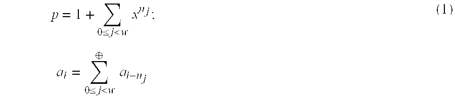
- each position a i in the PRBS bit sequence can be formed as follows, using (w ⁇ 1) XOR operations:
- U.S. Pat. No. 5,034,906 describes a system for synchronizing a pseudorandom binary sequence signal with a time-delayed version of the same signal without the use of delay lines or programmable counters. This is accomplished by the use of two Pseudorandom Binary Sequence [PRBS] generators for producing the same PRBS signal.
- PRBS Pseudorandom Binary Sequence
- Each PRBS generator incorporates as a constituent component a serial shift register with M stages with the outputs of multiple stages fed back through can exclusive-OR to provide an input to the register, thereby to produce a clocked repetitive series of said sequence signal as inputs to each register.
- the states of shift register are numbered n such that (n ⁇ 1) clock cycles elapse before the next start state.
- a start detect circuit is responsive to the start state of the pseudorandom binary sequence signal of the first generator for generating a synchronizing signal at that instant to force the second PRBS generator to be at a state in the binary sequence representing a delayed
- the main object of the invention is to achieve generation of quite a wide (S-bit long) pattern during a minimal “time clock” of the generator, i.e. to provide a method and a device for high speed PRBS generation.
- An additional object of the invention is to provide a high speed PRBS generator with effective capacity of the memory.
- the Inventors propose a novel solution of a high speed PRBS generator for a wide bus having width S (i.e., a parallel generator of S-long PRBS patterns) which is capable of performing calculations required for preparing an S-long PRBS pattern without any iterations, i.e., enables obtaining all bits of the PRBS pattern in parallel by performing for each bit a constant number N of logical operations according to a given polynomial, thus achieving the shortest possible clock period of the generator.
- S i.e., a parallel generator of S-long PRBS patterns
- PRBS pattern is used for defining a part of a PRBS sequence to be calculated and transmitted in parallel.
- this constant number N is the minimal number of operations required by the given polynomial.
- the minimal number of logical operations (XORs) to be performed per bit of the pattern is equal to w ⁇ 1.
- the minimal clock will be therefore limited by w ⁇ 1 XOR operations.
- the total minimal number of XOR circuits for the pattern will be S(w ⁇ 1).
- the high speed PRBS generator can be built if, per one bit of the S-bit long PRBS pattern, there is used a group of devices comprising the constant (and even a minimal number “w ⁇ 1”) of XORs, and if all S groups of XORs are operative simultaneously, thus providing for a shortened (and even the minimal) time clock.
- its memory is to be built as a number of S-long registers for storing previously issued PRBS patterns, and should be used in a special manner.
- the Lemma can be proven by induction as follows:
- the meaning of the Lemma is that instead of sequentially calculating every bit of a PRBS pattern using previous bits of this same pattern, one may perform separate calculation of each bit of the pattern based on “pre-previous” bits of the PRBS pattern, if stored in a memory.
- the degree of retroaction is measured by the power “t” (retrospective index); it can be selected so that all bits of the current PRBS pattern, including those requiring the longest history, be formed using the memory.
- M i is a running bit of memory M; it has a negative index expressing how old is the memory bit regarding to the corresponding current bit of the PRBS pattern created on the bus;
- t is a retrospective index selected so as to find the bit (2 t n j ), ready in the memory, for a specific bit b i of the current PRBS pattern.
- the memory comprises a number of S-long registers for storing previous issued PRBS patterns
- the Inventors estimated the effective capacity of the PRBS generator's memory based on the required length S of the pattern, value of “t” and complexity of the polynomial which is expressed by the parameter n J .
- FIG. 1 illustrates a conventional model for obtaining a PRBS sequence
- FIG. 2 illustrates a schematic block diagram of one embodiment of the proposed PRBS generator
- FIG. 3 gives an illustrative example of obtaining a PRBS pattern for an S-wide bus using the generator shown in FIG. 2.
- FIG. 2 illustrates a schematic block-diagram of one embodiment of the PRBS generator 14 according to the invention, which also explains the proposed method.
- the generator 14 comprises a memory 16 and is connected to an S-bit wide bus 15 to create on it a PRBS pattern in the form of a parallel burst of bits.
- a register 17 can be added between the generator and the bus.
- Each bit of the bus 15 is calculated using the memory 16 and an assembly 18 of logical units performing XOR operations and associated with a particular bit of the bus.
- each assembly 18 comprises only one XOR unit; it should be understood that more complex assemblies will be used if a more complex polynomial is given for creating the required PRBS pattern.
- the memory 16 comprises a plurality of registers, capable of performing parallel shift from the top register 22 to the direction of the bottom register 24 .
- Each of the registers stores a particular PRBS pattern (a part of the PRBS sequence); the “freshest” pattern is introduced in the memory upon completing its calculation (see arrows 26 ) and simultaneously with bursting it on to the bus 15 , while the “oldest” pattern is erased from the bottom pattern 24 due to feeding there-into a “fresher” pattern from the adjacent register.
- the process is controlled by a clock 20 .
- the corresponding assembly 18 uses particular bits in the memory which are located in previous PRBS patterns.
- FIG. 3 shows how a PRBS sequence 1+X 9 +X 11 can be obtained by the described generator.
- the bus width S 128.
- Positions of the top register 34 of the memory are indicated as M ⁇ 128 , M ⁇ 127 , . . . , M ⁇ 2 , M ⁇ 1 to express their previous state in time with respect to respective positions of the bus.
- contents of the top register 34 of the memory are shifted into the next register 36 .
- each bit of a particular PRBS pattern is calculated:
Abstract
Description
- The invention relates to a technique for generating Pseudo Random Binary Sequence (PRBS) for a wide bus (the bus having a large number S of binary positions to be transmitted in parallel), i.e. to a method and a device for periodically creating and transmitting a pseudo-random pattern comprising S bits.
- Creation of a PRBS is usually explained and implemented as applying a polynomial to a binary sequence; it can be illustrated by applying a number of XOR (exclusive OR) operations to a binary shift register.
- FIG. 1 shows a simple model for PRBS generation illustrating a
shift register 10 comprising oneXOR unit 12 which performs a logical operation of exclusive OR with the 11th and 9th positions of the register to introduce the result in the 0-th position of the register. The output of the register issues a PRBS bit sequence. - The process of forming the bit sequence can be described by the following polynomial having two terms (i.e., w=2, not including the “1”):
- P=1+X 9 +X 11
- According to the above polynomial, each position a i in the PRBS bit sequence can be formed as follows, using (w−1) XOR operations:
- a i =a i−9 ⊕a i−11
- Using indexes n j of complexity of a polynomial:
- a i =a i−n
0 ⊕a i−nj - where n 0=9, n1=11,
- we may write down the process of forming a PRBS based on any given polynomial:
- As it has been accepted by now, the greater the “w” parameter, the wider the bus (i.e., the greater the number of the “S” parameter), the more complex the PRBS generation process will be from the point of time and memory consumption.
- The above statement could be explained by the fact that, for forming any next binary position of the PRBS sequence, some particular previous binary positions of the PRBS sequence should be used. Based on the conventional model of the PRBS generation, one cannot calculate a following position of the PRBS sequence before the required previous positions of the sequence become known. However, the previous positions are also to be calculated based on some pre-previous positions of the PRBS stream. Consequently, if all S positions of a rather long pattern of PRBS sequence is to be created during one and the same generator's clock, this clock would most probably include a considerable number of iterative calculations (and a chain of XORs in the implementation) which means that a high speed clock is hardly achievable for wide buses.
- In case the PRBS sequence be wholly stored in the memory, so that patterns of the sequence be issued just by reading them from the memory one after another, the memory would be excessively large since the periodicity of a complex PRBS pattern is quite great and is equal to 2 K−1, where K=nw−1.
- U.S. Pat. No. 5,034,906 describes a system for synchronizing a pseudorandom binary sequence signal with a time-delayed version of the same signal without the use of delay lines or programmable counters. This is accomplished by the use of two Pseudorandom Binary Sequence [PRBS] generators for producing the same PRBS signal. Each PRBS generator incorporates as a constituent component a serial shift register with M stages with the outputs of multiple stages fed back through can exclusive-OR to provide an input to the register, thereby to produce a clocked repetitive series of said sequence signal as inputs to each register. The states of shift register are numbered n such that (n−1) clock cycles elapse before the next start state. A start detect circuit is responsive to the start state of the pseudorandom binary sequence signal of the first generator for generating a synchronizing signal at that instant to force the second PRBS generator to be at a state in the binary sequence representing a delayed point in the sequence.
- The solution of U.S. Pat. No. 5,034,906 is focussed on synchronizing the sequence. It should be mentioned, however, that the principle of a serial shift register does not allow obtaining a high speed wide bus PRBS generator.
- The main object of the invention is to achieve generation of quite a wide (S-bit long) pattern during a minimal “time clock” of the generator, i.e. to provide a method and a device for high speed PRBS generation. An additional object of the invention is to provide a high speed PRBS generator with effective capacity of the memory.
- The Inventors propose a novel solution of a high speed PRBS generator for a wide bus having width S (i.e., a parallel generator of S-long PRBS patterns) which is capable of performing calculations required for preparing an S-long PRBS pattern without any iterations, i.e., enables obtaining all bits of the PRBS pattern in parallel by performing for each bit a constant number N of logical operations according to a given polynomial, thus achieving the shortest possible clock period of the generator.
- The term “PRBS pattern” is used for defining a part of a PRBS sequence to be calculated and transmitted in parallel.
- Keeping in mind the facts that the pattern is calculated per bit, that the process is parallel, and that the number N of logical operations required for each bit of the pattern is constant, one may conclude that the complexity of processing is independent from the length S of the pattern (or from the width S of the bus).
- Preferably, this constant number N is the minimal number of operations required by the given polynomial.
- Speaking exactly, if the number of members of the given polynomial is w, the minimal number of logical operations (XORs) to be performed per bit of the pattern is equal to w−1. The minimal clock will be therefore limited by w−1 XOR operations. The total minimal number of XOR circuits for the pattern will be S(w−1).
- It should be mentioned, however, that the XOR operations do not have to be performed in sequence, i.e., in most cases some of them may be done in parallel. Therefore, the minimal time for per-bit calculation, measured in XORs (time for performing one XOR operation) is O(log w) where O is constant.
- The Inventors have therefore found that the high speed PRBS generator can be built if, per one bit of the S-bit long PRBS pattern, there is used a group of devices comprising the constant (and even a minimal number “w−1”) of XORs, and if all S groups of XORs are operative simultaneously, thus providing for a shortened (and even the minimal) time clock.
- For implementing the above-proposed generator, its memory is to be built as a number of S-long registers for storing previously issued PRBS patterns, and should be used in a special manner.
- The Inventors proved a Lemma which allows converting the expression (1) for creating a PRBS pattern based on a given polynomial, into a form which enables avoiding iterative calculations of bits of the PRBS by effectively utilizing the memory.
- The Lemma states:

- The Lemma can be proven by induction as follows:
- For t=0:


- The meaning of the Lemma is that instead of sequentially calculating every bit of a PRBS pattern using previous bits of this same pattern, one may perform separate calculation of each bit of the pattern based on “pre-previous” bits of the PRBS pattern, if stored in a memory. The degree of retroaction is measured by the power “t” (retrospective index); it can be selected so that all bits of the current PRBS pattern, including those requiring the longest history, be formed using the memory.
- However, different “t” values can be selected for calculating different bits of the current PRBS pattern, and that finding can be utilized for minimizing the required memory capacity.
- In other words, for the S-bit PRBS pattern built for a S-width bus B:

- where
- bi—is a running bit of the bus B comprising (b 0,b1, . . . bi . . . BS−1)
- M i—is a running bit of memory M; it has a negative index expressing how old is the memory bit regarding to the corresponding current bit of the PRBS pattern created on the bus;
- t—is a retrospective index selected so as to find the bit (2 t nj), ready in the memory, for a specific bit bi of the current PRBS pattern.
- Keeping in mind, that the memory comprises a number of S-long registers for storing previous issued PRBS patterns, it can be further clarified that any current created PRBS pattern is shifted, in parallel, into the memory and in the memory, which fact can be written down as follows:

- Moreover, the Inventors estimated the effective capacity of the PRBS generator's memory based on the required length S of the pattern, value of “t” and complexity of the polynomial which is expressed by the parameter n J.
- It has been found that the minimal value of “t” sufficient for forming any bit of the S-bit PRBS pattern by parallel calculation of all the bits (when one and the same “t” is used) will be:

- where n w−1>nw−2> . . . >n0
- Since the term of the polynomial having the complexity index n w−1 requires the most “deep” use of the memory, the memory capacity (in bits) C can be calculated as follows:

- The Inventors have shown that since different “t” values can be used for calculating different bits of the PRBS, the memory capacity can be further reduced:
- c′=2t m ·n w−1−2t m −1 =c−2t m −1 (7)
- Indeed, not all bits of the PRBS pattern require the same depth of the memory; for example, for bit b 0 the minimal t=0 can be used, i.e. the previous PRBS pattern just stored in the memory.
- The invention can be better understood with the aid of the following non-limiting drawings in which:
- FIG. 1 illustrates a conventional model for obtaining a PRBS sequence
- FIG. 2 illustrates a schematic block diagram of one embodiment of the proposed PRBS generator
- FIG. 3 gives an illustrative example of obtaining a PRBS pattern for an S-wide bus using the generator shown in FIG. 2.
- FIG. 2 illustrates a schematic block-diagram of one embodiment of the
PRBS generator 14 according to the invention, which also explains the proposed method. - The
generator 14 comprises amemory 16 and is connected to an S-bitwide bus 15 to create on it a PRBS pattern in the form of a parallel burst of bits. For synchronizing purposes only, aregister 17 can be added between the generator and the bus. Each bit of thebus 15 is calculated using thememory 16 and anassembly 18 of logical units performing XOR operations and associated with a particular bit of the bus. There are S such assemblies capable of working in parallel, and they form part of thegenerator 14. In the drawing, eachassembly 18 comprises only one XOR unit; it should be understood that more complex assemblies will be used if a more complex polynomial is given for creating the required PRBS pattern. - The
memory 16 comprises a plurality of registers, capable of performing parallel shift from thetop register 22 to the direction of thebottom register 24. Each of the registers stores a particular PRBS pattern (a part of the PRBS sequence); the “freshest” pattern is introduced in the memory upon completing its calculation (see arrows 26) and simultaneously with bursting it on to thebus 15, while the “oldest” pattern is erased from thebottom pattern 24 due to feeding there-into a “fresher” pattern from the adjacent register. The process is controlled by aclock 20. - For calculating a specific bit of a PRBS pattern, the corresponding
assembly 18 uses particular bits in the memory which are located in previous PRBS patterns. The required memory bits for each particular PRBS bit (bit of the bus) can be found using the Lemma, equation (3) and upon selecting the retrospective index “t”: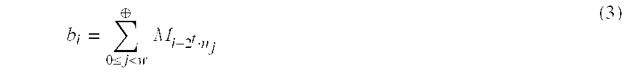
- The calculations are performed in parallel, using one and the same number of logical operations (which is preferably minimal and equals to w−1), due to that the calculation time is independent from the length of the pattern (i.e., from the width of the bus). Results of the S parallel calculations are synchronously fed to the
bus 15, and simultaneously and synchronously “shifted back” to respective bits of theregister 22. - FIG. 3 shows how a
PRBS sequence 1+X9+X11 can be obtained by the described generator. In this example, the bus width S=128.Positions 30 of the bus b0, b1, . . . b127, whenever obtained bylogical XOR assemblies 31, are transmitted over the bus and, at the same time clock, are shifted in parallel back to thememory 32. Positions of thetop register 34 of the memory are indicated as M−128, M−127, . . . , M−2, M−1 to express their previous state in time with respect to respective positions of the bus. At the next clock, contents of thetop register 34 of the memory are shifted into thenext register 36. - Using formula (5), the minimal value of the retrospective index t m can be calculated: tm=log2 (128/9)=4.
- Then, using formula (6), capacity C of the memory can be calculated as follows: C=2 4*11=176.
- It can be seen that for creating the required PRBS pattern for quite a wide bus (S=128), only 176 bits of memory are needed i.e., one complete register of 128 bits, and a second incomplete one. For creating this PRBS pattern in a conventional way, a much greater memory would be required.
- As has been mentioned, each bit of a particular PRBS pattern is calculated:
- based on a given polynomial having “w” members,
- independently from calculating other bits of the particular PRBS pattern, and
- using a constant number N of logical operations of exclusive OR, thereby enabling parallel calculation of all S bits of the particular PRBS pattern.
- In this embodiment, keeping in mind that:
- in the given polynomial we have two terms (w=2); n j takes two values equal to 11 and 9 respectively; and that N=1,
- we obtain particular positions of the PRBS pattern on the bus, using formula (3):
- b 0 =M (0−16*11) ⊕M 90−16*9) =M (−176) ⊕M (−144)
- . . .
- b 127 =M (127−176) ⊕M (127−144) =M (−49) ⊕M (−17).
- While the present invention has been described with reference to one particular example, it should be appreciated that other versions of the method and other implementations of the PRBS generator can be proposed based on the disclosed concept, which should all be considered part of the present invention.
Claims (12)


Applications Claiming Priority (2)
| Application Number | Priority Date | Filing Date | Title |
|---|---|---|---|
| IL147359A IL147359A (en) | 2001-12-27 | 2001-12-27 | Technique for high speed prbs generation |
| IL147359 | 2001-12-27 |
Publications (2)
| Publication Number | Publication Date |
|---|---|
| US20030126168A1 true US20030126168A1 (en) | 2003-07-03 |
| US7124158B2 US7124158B2 (en) | 2006-10-17 |
Family
ID=11075911
Family Applications (1)
| Application Number | Title | Priority Date | Filing Date |
|---|---|---|---|
| US10/329,581 Expired - Fee Related US7124158B2 (en) | 2001-12-27 | 2002-12-27 | Technique for high speed PRBS generation |
Country Status (2)
| Country | Link |
|---|---|
| US (1) | US7124158B2 (en) |
| IL (1) | IL147359A (en) |
Cited By (2)
| Publication number | Priority date | Publication date | Assignee | Title |
|---|---|---|---|---|
| KR101270590B1 (en) | 2011-11-19 | 2013-06-03 | 트라이콤텍 주식회사 | Scrambler in Next Generation DSRC System and Drive Method of the Same |
| CN107408032A (en) * | 2015-03-26 | 2017-11-28 | 英特尔公司 | PRBS pseudo-random bit sequence in interconnection |
Families Citing this family (8)
| Publication number | Priority date | Publication date | Assignee | Title |
|---|---|---|---|---|
| US20040024803A1 (en) * | 2002-07-31 | 2004-02-05 | Allen Montijo | Cascaded modified PRBS counters form easily programmed and efficient large counter |
| US7263540B1 (en) * | 2004-03-03 | 2007-08-28 | The United States Of America As Represented By The Director National Security Agency | Method of generating multiple random numbers |
| EP1792252A1 (en) * | 2004-09-22 | 2007-06-06 | Nokia Corporation | Method and apparatus for generating pseudo random numbers |
| US9116764B2 (en) * | 2007-04-17 | 2015-08-25 | Conversant Intellectual Property Management Inc. | Balanced pseudo-random binary sequence generator |
| US9124462B2 (en) | 2012-10-25 | 2015-09-01 | Texas Instruments Incorporated | Flexible PRBS architecture for a transceiver |
| US9401803B2 (en) | 2012-10-25 | 2016-07-26 | Texas Instruments Incorporated | Flexible scrambler/descrambler architecture for a transceiver |
| US10587437B2 (en) | 2013-06-10 | 2020-03-10 | Texas Instruments Incorporated | Link aggregator with universal packet scrambler apparatus and method |
| US9747076B1 (en) | 2014-12-04 | 2017-08-29 | Altera Corporation | Parallel pseudo random bit sequence generation with adjustable width |
Citations (7)
| Publication number | Priority date | Publication date | Assignee | Title |
|---|---|---|---|---|
| US5034906A (en) * | 1990-03-30 | 1991-07-23 | Microwave Logic | Pseudorandom Binary Sequence delay systems |
| US5224165A (en) * | 1988-10-25 | 1993-06-29 | Hughes Aircraft Company | High speed word generator |
| US5257282A (en) * | 1984-06-28 | 1993-10-26 | Unisys Corporation | High speed code sequence generator |
| US5519736A (en) * | 1993-09-09 | 1996-05-21 | Nec Corporation | Synchronous pseudo-noise code sequence generation circuit |
| US5796776A (en) * | 1995-06-30 | 1998-08-18 | Interdigital Technology Corporation | Code sequence generator in a CDMA modem |
| US6594680B1 (en) * | 1999-12-30 | 2003-07-15 | Texas Instruments Incorporated | Psuedo-random noise sequence generating system |
| US6735606B2 (en) * | 2001-05-15 | 2004-05-11 | Qualcomm Incorporated | Multi-sequence fast slewing pseudorandom noise generator |
-
2001
- 2001-12-27 IL IL147359A patent/IL147359A/en not_active IP Right Cessation
-
2002
- 2002-12-27 US US10/329,581 patent/US7124158B2/en not_active Expired - Fee Related
Patent Citations (7)
| Publication number | Priority date | Publication date | Assignee | Title |
|---|---|---|---|---|
| US5257282A (en) * | 1984-06-28 | 1993-10-26 | Unisys Corporation | High speed code sequence generator |
| US5224165A (en) * | 1988-10-25 | 1993-06-29 | Hughes Aircraft Company | High speed word generator |
| US5034906A (en) * | 1990-03-30 | 1991-07-23 | Microwave Logic | Pseudorandom Binary Sequence delay systems |
| US5519736A (en) * | 1993-09-09 | 1996-05-21 | Nec Corporation | Synchronous pseudo-noise code sequence generation circuit |
| US5796776A (en) * | 1995-06-30 | 1998-08-18 | Interdigital Technology Corporation | Code sequence generator in a CDMA modem |
| US6594680B1 (en) * | 1999-12-30 | 2003-07-15 | Texas Instruments Incorporated | Psuedo-random noise sequence generating system |
| US6735606B2 (en) * | 2001-05-15 | 2004-05-11 | Qualcomm Incorporated | Multi-sequence fast slewing pseudorandom noise generator |
Cited By (2)
| Publication number | Priority date | Publication date | Assignee | Title |
|---|---|---|---|---|
| KR101270590B1 (en) | 2011-11-19 | 2013-06-03 | 트라이콤텍 주식회사 | Scrambler in Next Generation DSRC System and Drive Method of the Same |
| CN107408032A (en) * | 2015-03-26 | 2017-11-28 | 英特尔公司 | PRBS pseudo-random bit sequence in interconnection |
Also Published As
| Publication number | Publication date |
|---|---|
| IL147359A (en) | 2007-03-08 |
| IL147359A0 (en) | 2002-08-14 |
| US7124158B2 (en) | 2006-10-17 |
Similar Documents
| Publication | Publication Date | Title |
|---|---|---|
| EP0066768A1 (en) | Apparatus for generation of random numbers | |
| EP2100219B9 (en) | Bit generator | |
| US7142675B2 (en) | Sequence generator and method of generating a pseudo random sequence | |
| US20030126168A1 (en) | Technique for high speed PRBS generation | |
| US20120278372A1 (en) | Cryptographic Random Number Generator Using Finite Field Operations | |
| JP5312318B2 (en) | Method and device for generating pseudo-random strings | |
| US9619206B2 (en) | Pseudo-random bit sequence generator | |
| US7340496B2 (en) | System and method for determining the Nth state of linear feedback shift registers | |
| US5323338A (en) | Pseudo-random sequence generators | |
| US8909510B2 (en) | LFSR emulation | |
| US6463448B1 (en) | Linear intrasummed multiple-bit feedback shift register | |
| JP2001251194A (en) | Crc arithmetic unit | |
| US20030014451A1 (en) | Method and machine for scrambling parallel data channels | |
| Mascia et al. | An algebraic attack on stream ciphers with application to nonlinear filter generators and WG-PRNG | |
| EP0280802B1 (en) | Generation of trigger signals | |
| WO2003096180A2 (en) | Fast multiplication circuits | |
| US7502814B2 (en) | Device and method for generating a pseudorandom sequence of numbers | |
| JPH11224183A (en) | Pseudo-random number generating device | |
| US20080263116A1 (en) | Balanced pseudo-random binary sequence generator | |
| JPS58129653A (en) | Multiplication system | |
| EP1451940B1 (en) | Apparatus and method for generating a code mask | |
| SU742910A1 (en) | Pseudorandom binary train generator | |
| JPH09181577A (en) | Pattern generation circuit | |
| JPH09251376A (en) | Safety evaluation device for pseudo random number generator for password/verification | |
| EP0665492A1 (en) | Pseudo-random series generator with increased frequency |
Legal Events
| Date | Code | Title | Description |
|---|---|---|---|
| AS | Assignment |
Owner name: LIGHTSCAPE NETWORKS, LTD., ISRAEL Free format text: ASSIGNMENT OF ASSIGNORS INTEREST;ASSIGNORS:RUTHSTEIN, JACOB;LITINSKY, LEV;SOMMER, RONEN;REEL/FRAME:014833/0337;SIGNING DATES FROM 20020103 TO 20030106 |
|
| AS | Assignment |
Owner name: ECI TELECOM LTD., ISRAEL Free format text: ASSIGNMENT OF ASSIGNORS INTEREST;ASSIGNOR:LIGHTSCAPE NETWORKS LTD.;REEL/FRAME:018219/0730 Effective date: 20030226 |
|
| AS | Assignment |
Owner name: CREDIT SUISSE, AS COLLATERAL AGENT, NEW YORK Free format text: SECURITY AGREEMENT;ASSIGNORS:EPSILON 1 LTD;ECI TELECOM LTD;LIGHTSCAPE NETWORKS LTD.;AND OTHERS;REEL/FRAME:020431/0705 Effective date: 20071214 |
|
| AS | Assignment |
Owner name: CREDIT SUISSE, CAYMAN ISLANDS BRANCH, AS COLLATERA Free format text: SECURITY AGREEMENT;ASSIGNORS:EPSILON 1 LTD.;ECI TELECOM LTD.;LIGHTSCAPE NETWORKS LTD.;AND OTHERS;REEL/FRAME:020442/0874 Effective date: 20071214 |
|
| FEPP | Fee payment procedure |
Free format text: PAYOR NUMBER ASSIGNED (ORIGINAL EVENT CODE: ASPN); ENTITY STATUS OF PATENT OWNER: LARGE ENTITY |
|
| FPAY | Fee payment |
Year of fee payment: 4 |
|
| FPAY | Fee payment |
Year of fee payment: 8 |
|
| AS | Assignment |
Owner name: CREDIT SUISSE AG, CAYMAN ISLANDS BRANCH, AS COLLAT Free format text: SECURITY AGREEMENT;ASSIGNORS:ECI TELECOM INC.;ECI TELECOM LTD.;EPSILON 1 LTD.;AND OTHERS;REEL/FRAME:033719/0084 Effective date: 20140813 Owner name: CREDIT SUISSE AG, CAYMAN ISLANDS BRANCH, AS COLLAT Free format text: ASSIGNMENT OF ASSIGNORS INTEREST;ASSIGNORS:ECI TELECOM INC.;ECI TELECOM LTD.;EPSILON 1 LTD.;AND OTHERS;REEL/FRAME:033719/0084 Effective date: 20140813 |
|
| AS | Assignment |
Owner name: EPSILON 1 LTD., ISRAEL Free format text: RELEASE BY SECURED PARTY;ASSIGNOR:CREDIT SUISSE AG, CAYMAN ISLANDS BRANCH, AS COLLATERAL AGENT;REEL/FRAME:045942/0140 Effective date: 20180329 Owner name: ECI TELECOM (UK) LIMITED, UNITED KINGDOM Free format text: RELEASE BY SECURED PARTY;ASSIGNOR:CREDIT SUISSE AG, CAYMAN ISLANDS BRANCH, AS COLLATERAL AGENT;REEL/FRAME:045942/0140 Effective date: 20180329 Owner name: ECI TELECOM INC., FLORIDA Free format text: RELEASE BY SECURED PARTY;ASSIGNOR:CREDIT SUISSE AG, CAYMAN ISLANDS BRANCH, AS COLLATERAL AGENT;REEL/FRAME:045942/0140 Effective date: 20180329 Owner name: TELECOM INVESTMENTS (FINANCE) LLC, DELAWARE Free format text: RELEASE BY SECURED PARTY;ASSIGNOR:CREDIT SUISSE AG, CAYMAN ISLANDS BRANCH, AS COLLATERAL AGENT;REEL/FRAME:045942/0140 Effective date: 20180329 Owner name: ECI TELECOM LTD., ISRAEL Free format text: RELEASE BY SECURED PARTY;ASSIGNOR:CREDIT SUISSE AG, CAYMAN ISLANDS BRANCH, AS COLLATERAL AGENT;REEL/FRAME:045942/0140 Effective date: 20180329 Owner name: ECI HOLDING (HUNGARY) KORLATOLT FELELOSSEGU TARSAS Free format text: RELEASE BY SECURED PARTY;ASSIGNOR:CREDIT SUISSE AG, CAYMAN ISLANDS BRANCH, AS COLLATERAL AGENT;REEL/FRAME:045942/0140 Effective date: 20180329 |
|
| FEPP | Fee payment procedure |
Free format text: MAINTENANCE FEE REMINDER MAILED (ORIGINAL EVENT CODE: REM.) |
|
| LAPS | Lapse for failure to pay maintenance fees |
Free format text: PATENT EXPIRED FOR FAILURE TO PAY MAINTENANCE FEES (ORIGINAL EVENT CODE: EXP.); ENTITY STATUS OF PATENT OWNER: LARGE ENTITY |
|
| STCH | Information on status: patent discontinuation |
Free format text: PATENT EXPIRED DUE TO NONPAYMENT OF MAINTENANCE FEES UNDER 37 CFR 1.362 |
|
| FP | Lapsed due to failure to pay maintenance fee |
Effective date: 20181017 |