US20030190812A1 - Electroless deposition method - Google Patents
Electroless deposition method Download PDFInfo
- Publication number
- US20030190812A1 US20030190812A1 US10/117,711 US11771102A US2003190812A1 US 20030190812 A1 US20030190812 A1 US 20030190812A1 US 11771102 A US11771102 A US 11771102A US 2003190812 A1 US2003190812 A1 US 2003190812A1
- Authority
- US
- United States
- Prior art keywords
- layer
- electroless
- cobalt
- substrate surface
- electroless solution
- Prior art date
- Legal status (The legal status is an assumption and is not a legal conclusion. Google has not performed a legal analysis and makes no representation as to the accuracy of the status listed.)
- Granted
Links
- 238000000151 deposition Methods 0.000 title claims abstract description 100
- 239000000758 substrate Substances 0.000 claims abstract description 133
- 238000000034 method Methods 0.000 claims abstract description 125
- 239000000243 solution Substances 0.000 claims abstract description 121
- 229910052751 metal Inorganic materials 0.000 claims abstract description 90
- 239000002184 metal Substances 0.000 claims abstract description 90
- 230000000977 initiatory effect Effects 0.000 claims abstract description 75
- 239000004020 conductor Substances 0.000 claims abstract description 69
- 238000004140 cleaning Methods 0.000 claims abstract description 39
- 230000004888 barrier function Effects 0.000 claims abstract description 38
- 229910000510 noble metal Inorganic materials 0.000 claims abstract description 38
- 229910021332 silicide Inorganic materials 0.000 claims abstract description 34
- FVBUAEGBCNSCDD-UHFFFAOYSA-N silicide(4-) Chemical compound [Si-4] FVBUAEGBCNSCDD-UHFFFAOYSA-N 0.000 claims abstract description 33
- 238000005530 etching Methods 0.000 claims abstract description 9
- 239000000203 mixture Substances 0.000 claims description 69
- 239000000463 material Substances 0.000 claims description 55
- 230000008021 deposition Effects 0.000 claims description 54
- 239000010941 cobalt Substances 0.000 claims description 52
- GUTLYIVDDKVIGB-UHFFFAOYSA-N cobalt atom Chemical compound [Co] GUTLYIVDDKVIGB-UHFFFAOYSA-N 0.000 claims description 52
- 230000008569 process Effects 0.000 claims description 51
- 229910017052 cobalt Inorganic materials 0.000 claims description 49
- 150000003839 salts Chemical class 0.000 claims description 35
- 238000000137 annealing Methods 0.000 claims description 28
- 239000003989 dielectric material Substances 0.000 claims description 28
- KDLHZDBZIXYQEI-UHFFFAOYSA-N Palladium Chemical compound [Pd] KDLHZDBZIXYQEI-UHFFFAOYSA-N 0.000 claims description 26
- 229910000531 Co alloy Inorganic materials 0.000 claims description 25
- VEXZGXHMUGYJMC-UHFFFAOYSA-N Hydrochloric acid Chemical compound Cl VEXZGXHMUGYJMC-UHFFFAOYSA-N 0.000 claims description 23
- BASFCYQUMIYNBI-UHFFFAOYSA-N platinum Chemical compound [Pt] BASFCYQUMIYNBI-UHFFFAOYSA-N 0.000 claims description 22
- RYGMFSIKBFXOCR-UHFFFAOYSA-N Copper Chemical compound [Cu] RYGMFSIKBFXOCR-UHFFFAOYSA-N 0.000 claims description 21
- 229910052802 copper Inorganic materials 0.000 claims description 21
- 239000010949 copper Substances 0.000 claims description 21
- KRHYYFGTRYWZRS-UHFFFAOYSA-N Fluorane Chemical compound F KRHYYFGTRYWZRS-UHFFFAOYSA-N 0.000 claims description 18
- QAOWNCQODCNURD-UHFFFAOYSA-N Sulfuric acid Chemical compound OS(O)(=O)=O QAOWNCQODCNURD-UHFFFAOYSA-N 0.000 claims description 17
- 150000007522 mineralic acids Chemical class 0.000 claims description 13
- 229910052763 palladium Inorganic materials 0.000 claims description 13
- 230000015572 biosynthetic process Effects 0.000 claims description 12
- 229910052697 platinum Inorganic materials 0.000 claims description 11
- 230000002378 acidificating effect Effects 0.000 claims description 10
- 238000005498 polishing Methods 0.000 claims description 9
- PIBWKRNGBLPSSY-UHFFFAOYSA-L palladium(II) chloride Chemical compound Cl[Pd]Cl PIBWKRNGBLPSSY-UHFFFAOYSA-L 0.000 claims description 7
- 150000003467 sulfuric acid derivatives Chemical class 0.000 claims description 7
- IIACRCGMVDHOTQ-UHFFFAOYSA-N sulfamic acid Chemical class NS(O)(=O)=O IIACRCGMVDHOTQ-UHFFFAOYSA-N 0.000 claims description 6
- QPLDLSVMHZLSFG-UHFFFAOYSA-N Copper oxide Chemical class [Cu]=O QPLDLSVMHZLSFG-UHFFFAOYSA-N 0.000 claims description 4
- QAOWNCQODCNURD-UHFFFAOYSA-L Sulfate Chemical compound [O-]S([O-])(=O)=O QAOWNCQODCNURD-UHFFFAOYSA-L 0.000 claims description 4
- 239000002210 silicon-based material Substances 0.000 claims description 4
- 239000007769 metal material Substances 0.000 claims description 3
- 150000003841 chloride salts Chemical class 0.000 claims 4
- 239000007864 aqueous solution Substances 0.000 claims 2
- 238000007598 dipping method Methods 0.000 claims 1
- UORVGPXVDQYIDP-UHFFFAOYSA-N borane Chemical compound B UORVGPXVDQYIDP-UHFFFAOYSA-N 0.000 abstract description 66
- 229910000085 borane Inorganic materials 0.000 abstract description 35
- 239000003638 chemical reducing agent Substances 0.000 abstract description 33
- 238000002161 passivation Methods 0.000 abstract description 22
- 239000003929 acidic solution Substances 0.000 abstract description 9
- HEMHJVSKTPXQMS-UHFFFAOYSA-M Sodium hydroxide Chemical compound [OH-].[Na+] HEMHJVSKTPXQMS-UHFFFAOYSA-M 0.000 description 27
- 238000005137 deposition process Methods 0.000 description 19
- XUIMIQQOPSSXEZ-UHFFFAOYSA-N Silicon Chemical compound [Si] XUIMIQQOPSSXEZ-UHFFFAOYSA-N 0.000 description 18
- 239000010703 silicon Substances 0.000 description 18
- 229910052710 silicon Inorganic materials 0.000 description 17
- RJTANRZEWTUVMA-UHFFFAOYSA-N boron;n-methylmethanamine Chemical compound [B].CNC RJTANRZEWTUVMA-UHFFFAOYSA-N 0.000 description 16
- -1 copper oxides Chemical class 0.000 description 16
- WFKWXMTUELFFGS-UHFFFAOYSA-N tungsten Chemical compound [W] WFKWXMTUELFFGS-UHFFFAOYSA-N 0.000 description 15
- 229910052721 tungsten Inorganic materials 0.000 description 15
- 239000010937 tungsten Substances 0.000 description 15
- 239000003795 chemical substances by application Substances 0.000 description 12
- KWYUFKZDYYNOTN-UHFFFAOYSA-M Potassium hydroxide Chemical compound [OH-].[K+] KWYUFKZDYYNOTN-UHFFFAOYSA-M 0.000 description 11
- 239000008367 deionised water Substances 0.000 description 11
- 238000005240 physical vapour deposition Methods 0.000 description 11
- XLYOFNOQVPJJNP-UHFFFAOYSA-N water Chemical compound O XLYOFNOQVPJJNP-UHFFFAOYSA-N 0.000 description 11
- 239000000654 additive Substances 0.000 description 10
- 238000005229 chemical vapour deposition Methods 0.000 description 10
- 229910021641 deionized water Inorganic materials 0.000 description 10
- VYPSYNLAJGMNEJ-UHFFFAOYSA-N Silicium dioxide Chemical compound O=[Si]=O VYPSYNLAJGMNEJ-UHFFFAOYSA-N 0.000 description 8
- JPNWDVUTVSTKMV-UHFFFAOYSA-N cobalt tungsten Chemical compound [Co].[W] JPNWDVUTVSTKMV-UHFFFAOYSA-N 0.000 description 8
- 229910021420 polycrystalline silicon Inorganic materials 0.000 description 8
- 229920005591 polysilicon Polymers 0.000 description 8
- 238000009713 electroplating Methods 0.000 description 7
- 239000010936 titanium Substances 0.000 description 7
- MHAJPDPJQMAIIY-UHFFFAOYSA-N Hydrogen peroxide Chemical compound OO MHAJPDPJQMAIIY-UHFFFAOYSA-N 0.000 description 6
- 229910001080 W alloy Inorganic materials 0.000 description 6
- CPJYFACXEHYLFS-UHFFFAOYSA-N [B].[W].[Co] Chemical compound [B].[W].[Co] CPJYFACXEHYLFS-UHFFFAOYSA-N 0.000 description 6
- FEBFYWHXKVOHDI-UHFFFAOYSA-N [Co].[P][W] Chemical compound [Co].[P][W] FEBFYWHXKVOHDI-UHFFFAOYSA-N 0.000 description 6
- 230000003197 catalytic effect Effects 0.000 description 6
- WDHWFGNRFMPTQS-UHFFFAOYSA-N cobalt tin Chemical compound [Co].[Sn] WDHWFGNRFMPTQS-UHFFFAOYSA-N 0.000 description 6
- 239000011521 glass Substances 0.000 description 6
- 229910044991 metal oxide Inorganic materials 0.000 description 6
- 150000004706 metal oxides Chemical class 0.000 description 6
- 238000001465 metallisation Methods 0.000 description 6
- 239000003002 pH adjusting agent Substances 0.000 description 6
- 229910052715 tantalum Inorganic materials 0.000 description 6
- GUVRBAGPIYLISA-UHFFFAOYSA-N tantalum atom Chemical compound [Ta] GUVRBAGPIYLISA-UHFFFAOYSA-N 0.000 description 6
- KWSLGOVYXMQPPX-UHFFFAOYSA-N 5-[3-(trifluoromethyl)phenyl]-2h-tetrazole Chemical compound FC(F)(F)C1=CC=CC(C2=NNN=N2)=C1 KWSLGOVYXMQPPX-UHFFFAOYSA-N 0.000 description 5
- QTBSBXVTEAMEQO-UHFFFAOYSA-N Acetic acid Chemical compound CC(O)=O QTBSBXVTEAMEQO-UHFFFAOYSA-N 0.000 description 5
- RTAQQCXQSZGOHL-UHFFFAOYSA-N Titanium Chemical compound [Ti] RTAQQCXQSZGOHL-UHFFFAOYSA-N 0.000 description 5
- GVPFVAHMJGGAJG-UHFFFAOYSA-L cobalt dichloride Chemical group [Cl-].[Cl-].[Co+2] GVPFVAHMJGGAJG-UHFFFAOYSA-L 0.000 description 5
- 229940044175 cobalt sulfate Drugs 0.000 description 5
- 229910000361 cobalt sulfate Inorganic materials 0.000 description 5
- KTVIXTQDYHMGHF-UHFFFAOYSA-L cobalt(2+) sulfate Chemical compound [Co+2].[O-]S([O-])(=O)=O KTVIXTQDYHMGHF-UHFFFAOYSA-L 0.000 description 5
- 239000008139 complexing agent Substances 0.000 description 5
- 239000004065 semiconductor Substances 0.000 description 5
- 229910001379 sodium hypophosphite Inorganic materials 0.000 description 5
- 239000004094 surface-active agent Substances 0.000 description 5
- 229910052719 titanium Inorganic materials 0.000 description 5
- VHUUQVKOLVNVRT-UHFFFAOYSA-N Ammonium hydroxide Chemical compound [NH4+].[OH-] VHUUQVKOLVNVRT-UHFFFAOYSA-N 0.000 description 4
- ZOXJGFHDIHLPTG-UHFFFAOYSA-N Boron Chemical compound [B] ZOXJGFHDIHLPTG-UHFFFAOYSA-N 0.000 description 4
- AEMRFAOFKBGASW-UHFFFAOYSA-N Glycolic acid Chemical compound OCC(O)=O AEMRFAOFKBGASW-UHFFFAOYSA-N 0.000 description 4
- XEEYBQQBJWHFJM-UHFFFAOYSA-N Iron Chemical compound [Fe] XEEYBQQBJWHFJM-UHFFFAOYSA-N 0.000 description 4
- PXHVJJICTQNCMI-UHFFFAOYSA-N Nickel Chemical compound [Ni] PXHVJJICTQNCMI-UHFFFAOYSA-N 0.000 description 4
- 229910001096 P alloy Inorganic materials 0.000 description 4
- OAICVXFJPJFONN-UHFFFAOYSA-N Phosphorus Chemical compound [P] OAICVXFJPJFONN-UHFFFAOYSA-N 0.000 description 4
- 229910001128 Sn alloy Inorganic materials 0.000 description 4
- ATJFFYVFTNAWJD-UHFFFAOYSA-N Tin Chemical compound [Sn] ATJFFYVFTNAWJD-UHFFFAOYSA-N 0.000 description 4
- NRTOMJZYCJJWKI-UHFFFAOYSA-N Titanium nitride Chemical compound [Ti]#N NRTOMJZYCJJWKI-UHFFFAOYSA-N 0.000 description 4
- 229910052796 boron Inorganic materials 0.000 description 4
- 238000006243 chemical reaction Methods 0.000 description 4
- 150000001875 compounds Chemical class 0.000 description 4
- QPJSUIGXIBEQAC-UHFFFAOYSA-N n-(2,4-dichloro-5-propan-2-yloxyphenyl)acetamide Chemical compound CC(C)OC1=CC(NC(C)=O)=C(Cl)C=C1Cl QPJSUIGXIBEQAC-UHFFFAOYSA-N 0.000 description 4
- SIBIBHIFKSKVRR-UHFFFAOYSA-N phosphanylidynecobalt Chemical compound [Co]#P SIBIBHIFKSKVRR-UHFFFAOYSA-N 0.000 description 4
- 229910052698 phosphorus Inorganic materials 0.000 description 4
- 239000011574 phosphorus Substances 0.000 description 4
- 239000003870 refractory metal Substances 0.000 description 4
- 239000000377 silicon dioxide Substances 0.000 description 4
- 235000012239 silicon dioxide Nutrition 0.000 description 4
- 239000001509 sodium citrate Substances 0.000 description 4
- NLJMYIDDQXHKNR-UHFFFAOYSA-K sodium citrate Chemical compound O.O.[Na+].[Na+].[Na+].[O-]C(=O)CC(O)(CC([O-])=O)C([O-])=O NLJMYIDDQXHKNR-UHFFFAOYSA-K 0.000 description 4
- XMVONEAAOPAGAO-UHFFFAOYSA-N sodium tungstate Chemical compound [Na+].[Na+].[O-][W]([O-])(=O)=O XMVONEAAOPAGAO-UHFFFAOYSA-N 0.000 description 4
- 239000003381 stabilizer Substances 0.000 description 4
- MZLGASXMSKOWSE-UHFFFAOYSA-N tantalum nitride Chemical compound [Ta]#N MZLGASXMSKOWSE-UHFFFAOYSA-N 0.000 description 4
- WGTYBPLFGIVFAS-UHFFFAOYSA-M tetramethylammonium hydroxide Chemical compound [OH-].C[N+](C)(C)C WGTYBPLFGIVFAS-UHFFFAOYSA-M 0.000 description 4
- UMGDCJDMYOKAJW-UHFFFAOYSA-N thiourea Chemical compound NC(N)=S UMGDCJDMYOKAJW-UHFFFAOYSA-N 0.000 description 4
- 239000011135 tin Substances 0.000 description 4
- 229910052718 tin Inorganic materials 0.000 description 4
- GRYLNZFGIOXLOG-UHFFFAOYSA-N Nitric acid Chemical compound O[N+]([O-])=O GRYLNZFGIOXLOG-UHFFFAOYSA-N 0.000 description 3
- 239000002253 acid Substances 0.000 description 3
- 229910045601 alloy Inorganic materials 0.000 description 3
- 239000000956 alloy Substances 0.000 description 3
- 229910052782 aluminium Inorganic materials 0.000 description 3
- XAGFODPZIPBFFR-UHFFFAOYSA-N aluminium Chemical compound [Al] XAGFODPZIPBFFR-UHFFFAOYSA-N 0.000 description 3
- 239000002585 base Substances 0.000 description 3
- 150000001735 carboxylic acids Chemical class 0.000 description 3
- 150000001805 chlorine compounds Chemical class 0.000 description 3
- 238000009792 diffusion process Methods 0.000 description 3
- IXCSERBJSXMMFS-UHFFFAOYSA-N hcl hcl Chemical compound Cl.Cl IXCSERBJSXMMFS-UHFFFAOYSA-N 0.000 description 3
- 150000002500 ions Chemical class 0.000 description 3
- 150000002739 metals Chemical class 0.000 description 3
- 229910017604 nitric acid Inorganic materials 0.000 description 3
- 239000002245 particle Substances 0.000 description 3
- ACVYVLVWPXVTIT-UHFFFAOYSA-M phosphinate Chemical compound [O-][PH2]=O ACVYVLVWPXVTIT-UHFFFAOYSA-M 0.000 description 3
- 239000012279 sodium borohydride Substances 0.000 description 3
- 229910000033 sodium borohydride Inorganic materials 0.000 description 3
- 238000005507 spraying Methods 0.000 description 3
- 239000000126 substance Substances 0.000 description 3
- NLXLAEXVIDQMFP-UHFFFAOYSA-N Ammonia chloride Chemical compound [NH4+].[Cl-] NLXLAEXVIDQMFP-UHFFFAOYSA-N 0.000 description 2
- XKRFYHLGVUSROY-UHFFFAOYSA-N Argon Chemical compound [Ar] XKRFYHLGVUSROY-UHFFFAOYSA-N 0.000 description 2
- IJGRMHOSHXDMSA-UHFFFAOYSA-N Atomic nitrogen Chemical compound N#N IJGRMHOSHXDMSA-UHFFFAOYSA-N 0.000 description 2
- 229910000521 B alloy Inorganic materials 0.000 description 2
- OKTJSMMVPCPJKN-UHFFFAOYSA-N Carbon Chemical compound [C] OKTJSMMVPCPJKN-UHFFFAOYSA-N 0.000 description 2
- 241000393496 Electra Species 0.000 description 2
- 229910000640 Fe alloy Inorganic materials 0.000 description 2
- OAKJQQAXSVQMHS-UHFFFAOYSA-N Hydrazine Chemical compound NN OAKJQQAXSVQMHS-UHFFFAOYSA-N 0.000 description 2
- UFHFLCQGNIYNRP-UHFFFAOYSA-N Hydrogen Chemical compound [H][H] UFHFLCQGNIYNRP-UHFFFAOYSA-N 0.000 description 2
- ZOKXTWBITQBERF-UHFFFAOYSA-N Molybdenum Chemical compound [Mo] ZOKXTWBITQBERF-UHFFFAOYSA-N 0.000 description 2
- 229910000990 Ni alloy Inorganic materials 0.000 description 2
- 229910004156 TaNx Inorganic materials 0.000 description 2
- 229910010421 TiNx Inorganic materials 0.000 description 2
- 229910021627 Tin(IV) chloride Inorganic materials 0.000 description 2
- XSQUKJJJFZCRTK-UHFFFAOYSA-N Urea Natural products NC(N)=O XSQUKJJJFZCRTK-UHFFFAOYSA-N 0.000 description 2
- QXZUUHYBWMWJHK-UHFFFAOYSA-N [Co].[Ni] Chemical compound [Co].[Ni] QXZUUHYBWMWJHK-UHFFFAOYSA-N 0.000 description 2
- 230000000996 additive effect Effects 0.000 description 2
- 229910052783 alkali metal Inorganic materials 0.000 description 2
- 150000001340 alkali metals Chemical class 0.000 description 2
- 239000000908 ammonium hydroxide Substances 0.000 description 2
- 239000012298 atmosphere Substances 0.000 description 2
- WVMHLYQJPRXKLC-UHFFFAOYSA-N borane;n,n-dimethylmethanamine Chemical compound B.CN(C)C WVMHLYQJPRXKLC-UHFFFAOYSA-N 0.000 description 2
- HZEIHKAVLOJHDG-UHFFFAOYSA-N boranylidynecobalt Chemical compound [Co]#B HZEIHKAVLOJHDG-UHFFFAOYSA-N 0.000 description 2
- 239000006227 byproduct Substances 0.000 description 2
- 229910052799 carbon Inorganic materials 0.000 description 2
- 239000000084 colloidal system Substances 0.000 description 2
- 239000000356 contaminant Substances 0.000 description 2
- 238000004070 electrodeposition Methods 0.000 description 2
- 238000005516 engineering process Methods 0.000 description 2
- ZHPNWZCWUUJAJC-UHFFFAOYSA-N fluorosilicon Chemical compound [Si]F ZHPNWZCWUUJAJC-UHFFFAOYSA-N 0.000 description 2
- 239000007789 gas Substances 0.000 description 2
- 239000001257 hydrogen Substances 0.000 description 2
- 229910052739 hydrogen Inorganic materials 0.000 description 2
- 230000010354 integration Effects 0.000 description 2
- 229910052742 iron Inorganic materials 0.000 description 2
- UGKDIUIOSMUOAW-UHFFFAOYSA-N iron nickel Chemical compound [Fe].[Ni] UGKDIUIOSMUOAW-UHFFFAOYSA-N 0.000 description 2
- 238000001451 molecular beam epitaxy Methods 0.000 description 2
- 229910052750 molybdenum Inorganic materials 0.000 description 2
- 239000011733 molybdenum Substances 0.000 description 2
- 229910052759 nickel Inorganic materials 0.000 description 2
- 229910052758 niobium Inorganic materials 0.000 description 2
- 239000010955 niobium Substances 0.000 description 2
- GUCVJGMIXFAOAE-UHFFFAOYSA-N niobium atom Chemical compound [Nb] GUCVJGMIXFAOAE-UHFFFAOYSA-N 0.000 description 2
- 150000004767 nitrides Chemical class 0.000 description 2
- 238000000059 patterning Methods 0.000 description 2
- 229920002120 photoresistant polymer Polymers 0.000 description 2
- 229920000642 polymer Polymers 0.000 description 2
- 230000027756 respiratory electron transport chain Effects 0.000 description 2
- 229910052702 rhenium Inorganic materials 0.000 description 2
- WUAPFZMCVAUBPE-UHFFFAOYSA-N rhenium atom Chemical compound [Re] WUAPFZMCVAUBPE-UHFFFAOYSA-N 0.000 description 2
- 238000007086 side reaction Methods 0.000 description 2
- HBMJWWWQQXIZIP-UHFFFAOYSA-N silicon carbide Chemical compound [Si+]#[C-] HBMJWWWQQXIZIP-UHFFFAOYSA-N 0.000 description 2
- 229910010271 silicon carbide Inorganic materials 0.000 description 2
- LIVNPJMFVYWSIS-UHFFFAOYSA-N silicon monoxide Chemical class [Si-]#[O+] LIVNPJMFVYWSIS-UHFFFAOYSA-N 0.000 description 2
- 229910052814 silicon oxide Inorganic materials 0.000 description 2
- 229940074404 sodium succinate Drugs 0.000 description 2
- ZDQYSKICYIVCPN-UHFFFAOYSA-L sodium succinate (anhydrous) Chemical compound [Na+].[Na+].[O-]C(=O)CCC([O-])=O ZDQYSKICYIVCPN-UHFFFAOYSA-L 0.000 description 2
- 238000004544 sputter deposition Methods 0.000 description 2
- 125000005402 stannate group Chemical group 0.000 description 2
- HPGGPRDJHPYFRM-UHFFFAOYSA-J tin(iv) chloride Chemical compound Cl[Sn](Cl)(Cl)Cl HPGGPRDJHPYFRM-UHFFFAOYSA-J 0.000 description 2
- PBYZMCDFOULPGH-UHFFFAOYSA-N tungstate Chemical class [O-][W]([O-])(=O)=O PBYZMCDFOULPGH-UHFFFAOYSA-N 0.000 description 2
- CMPGARWFYBADJI-UHFFFAOYSA-L tungstic acid Chemical compound O[W](O)(=O)=O CMPGARWFYBADJI-UHFFFAOYSA-L 0.000 description 2
- 229910021503 Cobalt(II) hydroxide Inorganic materials 0.000 description 1
- 206010010144 Completed suicide Diseases 0.000 description 1
- 239000005751 Copper oxide Substances 0.000 description 1
- JPVYNHNXODAKFH-UHFFFAOYSA-N Cu2+ Chemical compound [Cu+2] JPVYNHNXODAKFH-UHFFFAOYSA-N 0.000 description 1
- CWYNVVGOOAEACU-UHFFFAOYSA-N Fe2+ Chemical compound [Fe+2] CWYNVVGOOAEACU-UHFFFAOYSA-N 0.000 description 1
- KJTLSVCANCCWHF-UHFFFAOYSA-N Ruthenium Chemical compound [Ru] KJTLSVCANCCWHF-UHFFFAOYSA-N 0.000 description 1
- 229910000676 Si alloy Inorganic materials 0.000 description 1
- BQCADISMDOOEFD-UHFFFAOYSA-N Silver Chemical compound [Ag] BQCADISMDOOEFD-UHFFFAOYSA-N 0.000 description 1
- ZMMUSLWEDSQDJY-UHFFFAOYSA-N [B].[Sn].[Co] Chemical compound [B].[Sn].[Co] ZMMUSLWEDSQDJY-UHFFFAOYSA-N 0.000 description 1
- YCOASTWZYJGKEK-UHFFFAOYSA-N [Co].[Ni].[W] Chemical compound [Co].[Ni].[W] YCOASTWZYJGKEK-UHFFFAOYSA-N 0.000 description 1
- 238000013019 agitation Methods 0.000 description 1
- 235000019270 ammonium chloride Nutrition 0.000 description 1
- 229910052786 argon Inorganic materials 0.000 description 1
- 238000005234 chemical deposition Methods 0.000 description 1
- 150000001868 cobalt Chemical class 0.000 description 1
- 229910000428 cobalt oxide Inorganic materials 0.000 description 1
- IVMYJDGYRUAWML-UHFFFAOYSA-N cobalt(ii) oxide Chemical compound [Co]=O IVMYJDGYRUAWML-UHFFFAOYSA-N 0.000 description 1
- 238000011109 contamination Methods 0.000 description 1
- 229910001431 copper ion Inorganic materials 0.000 description 1
- 229910000431 copper oxide Inorganic materials 0.000 description 1
- 239000008151 electrolyte solution Substances 0.000 description 1
- 238000005538 encapsulation Methods 0.000 description 1
- PCHJSUWPFVWCPO-UHFFFAOYSA-N gold Chemical compound [Au] PCHJSUWPFVWCPO-UHFFFAOYSA-N 0.000 description 1
- 229910052737 gold Inorganic materials 0.000 description 1
- 239000010931 gold Substances 0.000 description 1
- 238000010438 heat treatment Methods 0.000 description 1
- 239000001307 helium Substances 0.000 description 1
- 229910052734 helium Inorganic materials 0.000 description 1
- SWQJXJOGLNCZEY-UHFFFAOYSA-N helium atom Chemical compound [He] SWQJXJOGLNCZEY-UHFFFAOYSA-N 0.000 description 1
- 150000002431 hydrogen Chemical class 0.000 description 1
- 238000011065 in-situ storage Methods 0.000 description 1
- 229910052741 iridium Inorganic materials 0.000 description 1
- GKOZUEZYRPOHIO-UHFFFAOYSA-N iridium atom Chemical compound [Ir] GKOZUEZYRPOHIO-UHFFFAOYSA-N 0.000 description 1
- 238000004519 manufacturing process Methods 0.000 description 1
- 229910001092 metal group alloy Inorganic materials 0.000 description 1
- 229910021645 metal ion Inorganic materials 0.000 description 1
- WSFSSNUMVMOOMR-NJFSPNSNSA-N methanone Chemical compound O=[14CH2] WSFSSNUMVMOOMR-NJFSPNSNSA-N 0.000 description 1
- 230000004048 modification Effects 0.000 description 1
- 238000012986 modification Methods 0.000 description 1
- 229910052757 nitrogen Inorganic materials 0.000 description 1
- 229910052756 noble gas Inorganic materials 0.000 description 1
- 150000002835 noble gases Chemical class 0.000 description 1
- NJPPVKZQTLUDBO-UHFFFAOYSA-N novaluron Chemical compound C1=C(Cl)C(OC(F)(F)C(OC(F)(F)F)F)=CC=C1NC(=O)NC(=O)C1=C(F)C=CC=C1F NJPPVKZQTLUDBO-UHFFFAOYSA-N 0.000 description 1
- 230000006911 nucleation Effects 0.000 description 1
- 238000010899 nucleation Methods 0.000 description 1
- 229910052762 osmium Inorganic materials 0.000 description 1
- SYQBFIAQOQZEGI-UHFFFAOYSA-N osmium atom Chemical compound [Os] SYQBFIAQOQZEGI-UHFFFAOYSA-N 0.000 description 1
- RFLFDJSIZCCYIP-UHFFFAOYSA-L palladium(2+);sulfate Chemical compound [Pd+2].[O-]S([O-])(=O)=O RFLFDJSIZCCYIP-UHFFFAOYSA-L 0.000 description 1
- 238000007747 plating Methods 0.000 description 1
- 238000002203 pretreatment Methods 0.000 description 1
- 239000000047 product Substances 0.000 description 1
- 238000006722 reduction reaction Methods 0.000 description 1
- 229910052703 rhodium Inorganic materials 0.000 description 1
- 239000010948 rhodium Substances 0.000 description 1
- MHOVAHRLVXNVSD-UHFFFAOYSA-N rhodium atom Chemical compound [Rh] MHOVAHRLVXNVSD-UHFFFAOYSA-N 0.000 description 1
- 229910052707 ruthenium Inorganic materials 0.000 description 1
- 229910052709 silver Inorganic materials 0.000 description 1
- 239000004332 silver Substances 0.000 description 1
- 125000006850 spacer group Chemical group 0.000 description 1
- 229910002058 ternary alloy Inorganic materials 0.000 description 1
Images


Classifications
-
- H—ELECTRICITY
- H01—ELECTRIC ELEMENTS
- H01L—SEMICONDUCTOR DEVICES NOT COVERED BY CLASS H10
- H01L21/00—Processes or apparatus adapted for the manufacture or treatment of semiconductor or solid state devices or of parts thereof
- H01L21/70—Manufacture or treatment of devices consisting of a plurality of solid state components formed in or on a common substrate or of parts thereof; Manufacture of integrated circuit devices or of parts thereof
- H01L21/71—Manufacture of specific parts of devices defined in group H01L21/70
- H01L21/768—Applying interconnections to be used for carrying current between separate components within a device comprising conductors and dielectrics
- H01L21/76838—Applying interconnections to be used for carrying current between separate components within a device comprising conductors and dielectrics characterised by the formation and the after-treatment of the conductors
- H01L21/76841—Barrier, adhesion or liner layers
- H01L21/76843—Barrier, adhesion or liner layers formed in openings in a dielectric
-
- C—CHEMISTRY; METALLURGY
- C23—COATING METALLIC MATERIAL; COATING MATERIAL WITH METALLIC MATERIAL; CHEMICAL SURFACE TREATMENT; DIFFUSION TREATMENT OF METALLIC MATERIAL; COATING BY VACUUM EVAPORATION, BY SPUTTERING, BY ION IMPLANTATION OR BY CHEMICAL VAPOUR DEPOSITION, IN GENERAL; INHIBITING CORROSION OF METALLIC MATERIAL OR INCRUSTATION IN GENERAL
- C23C—COATING METALLIC MATERIAL; COATING MATERIAL WITH METALLIC MATERIAL; SURFACE TREATMENT OF METALLIC MATERIAL BY DIFFUSION INTO THE SURFACE, BY CHEMICAL CONVERSION OR SUBSTITUTION; COATING BY VACUUM EVAPORATION, BY SPUTTERING, BY ION IMPLANTATION OR BY CHEMICAL VAPOUR DEPOSITION, IN GENERAL
- C23C18/00—Chemical coating by decomposition of either liquid compounds or solutions of the coating forming compounds, without leaving reaction products of surface material in the coating; Contact plating
- C23C18/16—Chemical coating by decomposition of either liquid compounds or solutions of the coating forming compounds, without leaving reaction products of surface material in the coating; Contact plating by reduction or substitution, e.g. electroless plating
- C23C18/1601—Process or apparatus
- C23C18/1633—Process of electroless plating
- C23C18/1646—Characteristics of the product obtained
- C23C18/165—Multilayered product
- C23C18/1651—Two or more layers only obtained by electroless plating
-
- C—CHEMISTRY; METALLURGY
- C23—COATING METALLIC MATERIAL; COATING MATERIAL WITH METALLIC MATERIAL; CHEMICAL SURFACE TREATMENT; DIFFUSION TREATMENT OF METALLIC MATERIAL; COATING BY VACUUM EVAPORATION, BY SPUTTERING, BY ION IMPLANTATION OR BY CHEMICAL VAPOUR DEPOSITION, IN GENERAL; INHIBITING CORROSION OF METALLIC MATERIAL OR INCRUSTATION IN GENERAL
- C23C—COATING METALLIC MATERIAL; COATING MATERIAL WITH METALLIC MATERIAL; SURFACE TREATMENT OF METALLIC MATERIAL BY DIFFUSION INTO THE SURFACE, BY CHEMICAL CONVERSION OR SUBSTITUTION; COATING BY VACUUM EVAPORATION, BY SPUTTERING, BY ION IMPLANTATION OR BY CHEMICAL VAPOUR DEPOSITION, IN GENERAL
- C23C18/00—Chemical coating by decomposition of either liquid compounds or solutions of the coating forming compounds, without leaving reaction products of surface material in the coating; Contact plating
- C23C18/16—Chemical coating by decomposition of either liquid compounds or solutions of the coating forming compounds, without leaving reaction products of surface material in the coating; Contact plating by reduction or substitution, e.g. electroless plating
- C23C18/18—Pretreatment of the material to be coated
- C23C18/1851—Pretreatment of the material to be coated of surfaces of non-metallic or semiconducting in organic material
- C23C18/1872—Pretreatment of the material to be coated of surfaces of non-metallic or semiconducting in organic material by chemical pretreatment
- C23C18/1886—Multistep pretreatment
- C23C18/1893—Multistep pretreatment with use of organic or inorganic compounds other than metals, first
-
- H—ELECTRICITY
- H01—ELECTRIC ELEMENTS
- H01L—SEMICONDUCTOR DEVICES NOT COVERED BY CLASS H10
- H01L21/00—Processes or apparatus adapted for the manufacture or treatment of semiconductor or solid state devices or of parts thereof
- H01L21/02—Manufacture or treatment of semiconductor devices or of parts thereof
- H01L21/04—Manufacture or treatment of semiconductor devices or of parts thereof the devices having at least one potential-jump barrier or surface barrier, e.g. PN junction, depletion layer or carrier concentration layer
- H01L21/18—Manufacture or treatment of semiconductor devices or of parts thereof the devices having at least one potential-jump barrier or surface barrier, e.g. PN junction, depletion layer or carrier concentration layer the devices having semiconductor bodies comprising elements of Group IV of the Periodic System or AIIIBV compounds with or without impurities, e.g. doping materials
- H01L21/28—Manufacture of electrodes on semiconductor bodies using processes or apparatus not provided for in groups H01L21/20 - H01L21/268
- H01L21/283—Deposition of conductive or insulating materials for electrodes conducting electric current
- H01L21/285—Deposition of conductive or insulating materials for electrodes conducting electric current from a gas or vapour, e.g. condensation
- H01L21/28506—Deposition of conductive or insulating materials for electrodes conducting electric current from a gas or vapour, e.g. condensation of conductive layers
- H01L21/28512—Deposition of conductive or insulating materials for electrodes conducting electric current from a gas or vapour, e.g. condensation of conductive layers on semiconductor bodies comprising elements of Group IV of the Periodic System
- H01L21/28518—Deposition of conductive or insulating materials for electrodes conducting electric current from a gas or vapour, e.g. condensation of conductive layers on semiconductor bodies comprising elements of Group IV of the Periodic System the conductive layers comprising silicides
-
- H—ELECTRICITY
- H01—ELECTRIC ELEMENTS
- H01L—SEMICONDUCTOR DEVICES NOT COVERED BY CLASS H10
- H01L21/00—Processes or apparatus adapted for the manufacture or treatment of semiconductor or solid state devices or of parts thereof
- H01L21/02—Manufacture or treatment of semiconductor devices or of parts thereof
- H01L21/04—Manufacture or treatment of semiconductor devices or of parts thereof the devices having at least one potential-jump barrier or surface barrier, e.g. PN junction, depletion layer or carrier concentration layer
- H01L21/18—Manufacture or treatment of semiconductor devices or of parts thereof the devices having at least one potential-jump barrier or surface barrier, e.g. PN junction, depletion layer or carrier concentration layer the devices having semiconductor bodies comprising elements of Group IV of the Periodic System or AIIIBV compounds with or without impurities, e.g. doping materials
- H01L21/28—Manufacture of electrodes on semiconductor bodies using processes or apparatus not provided for in groups H01L21/20 - H01L21/268
- H01L21/283—Deposition of conductive or insulating materials for electrodes conducting electric current
- H01L21/288—Deposition of conductive or insulating materials for electrodes conducting electric current from a liquid, e.g. electrolytic deposition
-
- H—ELECTRICITY
- H01—ELECTRIC ELEMENTS
- H01L—SEMICONDUCTOR DEVICES NOT COVERED BY CLASS H10
- H01L21/00—Processes or apparatus adapted for the manufacture or treatment of semiconductor or solid state devices or of parts thereof
- H01L21/70—Manufacture or treatment of devices consisting of a plurality of solid state components formed in or on a common substrate or of parts thereof; Manufacture of integrated circuit devices or of parts thereof
- H01L21/71—Manufacture of specific parts of devices defined in group H01L21/70
- H01L21/768—Applying interconnections to be used for carrying current between separate components within a device comprising conductors and dielectrics
- H01L21/76838—Applying interconnections to be used for carrying current between separate components within a device comprising conductors and dielectrics characterised by the formation and the after-treatment of the conductors
- H01L21/76841—Barrier, adhesion or liner layers
- H01L21/76843—Barrier, adhesion or liner layers formed in openings in a dielectric
- H01L21/76849—Barrier, adhesion or liner layers formed in openings in a dielectric the layer being positioned on top of the main fill metal
-
- H—ELECTRICITY
- H01—ELECTRIC ELEMENTS
- H01L—SEMICONDUCTOR DEVICES NOT COVERED BY CLASS H10
- H01L21/00—Processes or apparatus adapted for the manufacture or treatment of semiconductor or solid state devices or of parts thereof
- H01L21/70—Manufacture or treatment of devices consisting of a plurality of solid state components formed in or on a common substrate or of parts thereof; Manufacture of integrated circuit devices or of parts thereof
- H01L21/71—Manufacture of specific parts of devices defined in group H01L21/70
- H01L21/768—Applying interconnections to be used for carrying current between separate components within a device comprising conductors and dielectrics
- H01L21/76838—Applying interconnections to be used for carrying current between separate components within a device comprising conductors and dielectrics characterised by the formation and the after-treatment of the conductors
- H01L21/76841—Barrier, adhesion or liner layers
- H01L21/76871—Layers specifically deposited to enhance or enable the nucleation of further layers, i.e. seed layers
- H01L21/76874—Layers specifically deposited to enhance or enable the nucleation of further layers, i.e. seed layers for electroless plating
-
- H—ELECTRICITY
- H01—ELECTRIC ELEMENTS
- H01L—SEMICONDUCTOR DEVICES NOT COVERED BY CLASS H10
- H01L29/00—Semiconductor devices adapted for rectifying, amplifying, oscillating or switching, or capacitors or resistors with at least one potential-jump barrier or surface barrier, e.g. PN junction depletion layer or carrier concentration layer; Details of semiconductor bodies or of electrodes thereof ; Multistep manufacturing processes therefor
- H01L29/66—Types of semiconductor device ; Multistep manufacturing processes therefor
- H01L29/66007—Multistep manufacturing processes
- H01L29/66075—Multistep manufacturing processes of devices having semiconductor bodies comprising group 14 or group 13/15 materials
- H01L29/66227—Multistep manufacturing processes of devices having semiconductor bodies comprising group 14 or group 13/15 materials the devices being controllable only by the electric current supplied or the electric potential applied, to an electrode which does not carry the current to be rectified, amplified or switched, e.g. three-terminal devices
- H01L29/66409—Unipolar field-effect transistors
- H01L29/66477—Unipolar field-effect transistors with an insulated gate, i.e. MISFET
- H01L29/665—Unipolar field-effect transistors with an insulated gate, i.e. MISFET using self aligned silicidation, i.e. salicide
-
- H—ELECTRICITY
- H01—ELECTRIC ELEMENTS
- H01L—SEMICONDUCTOR DEVICES NOT COVERED BY CLASS H10
- H01L2221/00—Processes or apparatus adapted for the manufacture or treatment of semiconductor or solid state devices or of parts thereof covered by H01L21/00
- H01L2221/10—Applying interconnections to be used for carrying current between separate components within a device
- H01L2221/1068—Formation and after-treatment of conductors
- H01L2221/1073—Barrier, adhesion or liner layers
- H01L2221/1084—Layers specifically deposited to enhance or enable the nucleation of further layers, i.e. seed layers
- H01L2221/1089—Stacks of seed layers
Definitions
- the present invention relates to the fabrication of semiconductor devices and to the apparatus and methods for deposition, removal, and modification of materials on a semiconductor substrate.
- copper and its alloys have become the metals of choice for sub-micron interconnect technology because copper has a lower resistivity than aluminum, (1.7 ⁇ -cm compared to 3.1 ⁇ -cm for aluminum), a higher current carrying capacity, and significantly higher electromigration resistance. These characteristics are important for supporting the higher current densities experienced at high levels of integration and increased device speed. Further, copper has a good thermal conductivity and is available in a highly pure state.
- Electroplating is one process being used to fill high aspect ratio features on substrates. Electroplating processes typically require a thin, electrically conductive seed layer to be deposited on the substrate. Electroplating is accomplished by applying an electrical current to the seed layer and exposing the substrate to an electrolytic solution containing metal ions that plate over the seed layer.
- Electroless deposition is another process used to deposit conductive materials. Although electroless deposition techniques have been widely used to deposit conductive metals over non-conductive printed circuit boards, electroless deposition techniques have not been extensively used for forming interconnects in VLSI and ULSI semiconductors. Electroless deposition involves an auto catalyzed chemical deposition process that does not require an applied current for a plating reaction to occur. Electroless deposition typically involves exposing a substrate to a solution by immersing the substrate in a bath or by spraying the solution over the substrate.
- oxides may also detrimentally affect subsequent processing.
- oxides may interfere with electroless deposition techniques. Electroless deposition techniques require a surface capable of electron transfer for nucleation, i.e., catalyzing, of a conductive material over that surface, and oxidized surfaces, for example on copper seed layers and metal barrier layers, cannot sufficiently participate in electron transfer for effective electroless deposition.
- One solution is to deposit a passivation layer or encapsulation layer on the metal layer to prevent metal oxide formation.
- Cobalt and cobalt alloys have been observed as suitable materials for passivating copper.
- Cobalt may also be deposited by electroless deposition techniques on copper.
- copper does not satisfactorily catalyze or initiate deposition of materials from electroless solutions.
- One solution is to initiate deposition from an electroless solution by contacting the copper substrate with a ferrous material that initiates deposition though a galvanic reaction. However, the process requires a continuous conductive surface over the substrate surface that may not be possible with some passivation applications.
- Another solution is to activate the copper surface by depositing a catalytic material on the copper surface.
- catalytic colloid compounds may adhere to dielectric materials and result in undesired, excessive, and non-selective deposition of the passivation material on the substrate surface.
- Non-selective deposition of passivation material may lead to surface contamination, unwanted diffusion of conductive materials into dielectric materials, and even device failure from short circuits and other device irregularities.
- Embodiments of the invention described herein generally provide methods and compositions for forming a metal or a metal silicide layer using an electroless deposition process.
- a method for processing a substrate including polishing a substrate surface to expose a first conductive material disposed in a dielectric material, depositing an initiation layer on the first conductive material, cleaning the substrate surface of the first electroless solution, and depositing a second conductive material on the initiation layer by exposing the initiation layer to an electroless solution.
- the initiation layer may be formed by exposing the substrate surface to a noble metal electroless solution.
- the second conductive material may be deposited as a passivation layer, a barrier layer, a seed layer, or for use in forming a metal silicide layer.
- a method for processing a substrate including polishing a substrate surface to expose a first conductive material disposed in a dielectric material, etching the substrate surface with an acidic solution, cleaning the substrate of the acidic solution, depositing an initiation layer selectively on the first conductive material by exposing the substrate surface to a first electroless solution, cleaning the substrate surface of the first electroless solution, and depositing a second conductive material on the initiation layer by exposing the initiation layer to a second electroless solution.
- the initiation layer may be formed by exposing the substrate surface to a noble metal electroless solution.
- the second conductive material may be deposited as a passivation layer, a barrier layer, a seed layer, or for use in forming a metal silicide layer.
- a method for processing a substrate including polishing a substrate surface to expose a first conductive material disposed in a dielectric material, exposing the substrate surface to a solution comprising a boron-containing reducing agent, forming initiation sites on the exposed first conductive material, and depositing a second conductive material on the initiation sites by exposing the substrate surface to an electroless solution containing a reducing agent.
- the second conductive material may be deposited as a passivation layer, a barrier layer, a seed layer, or for use in forming a metal silicide layer.
- a method for processing a substrate including polishing a substrate surface to expose a first conductive material disposed in a dielectric material and depositing a second conductive material on the first conductive metal by exposing the substrate surface to an electroless solution containing a boron-containing reducing agent.
- the second conductive material may be deposited as a passivation layer, a barrier layer, a seed layer, or for use in forming a metal silicide layer.
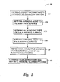
- FIG. 1 is a flow chart illustrating steps undertaken in depositing conductive layers according to one embodiment of the invention
- FIGS. 2 A- 2 C are schematic sectional views of one deposition process described herein;
- FIGS. 3 A- 3 C are schematic sectional views of one deposition process described herein.
- FIG. 4 is a simplified sectional view of a silicide material used as a contact with a transistor.
- Embodiments of the invention described herein provide methods and apparatus for depositing a conductive material by an electroless process.
- One material that may be deposited is cobalt or cobalt alloys, which may be deposited as a passivation layer, a barrier layer, a seed layer, or used in the formation of a metal silicide layer.
- Electroless deposition is broadly defined herein as deposition of a conductive material generally provided as charged ions in a bath over a catalytically active surface to deposit the conductive material by chemical reduction in the absence of an external electric current.
- Suitable apparatus include an ElectraTM ECP processing platform or LinkTM processing platform that are commercially available from Applied Materials, Inc., located in Santa Clara, Calif.
- the Electra CuTM ECP platform for example, includes an integrated processing chamber capable of depositing a conductive material by an electroless process, such as an electroless deposition processing (EDP) cell, which are commercially available from Applied Materials, Inc., located in Santa Clara, Calif.
- EDP electroless deposition processing
- the Electra CuTM ECP platform generally includes one or more electroless deposition processing (EDP) cells as well as one or more pre-deposition or post-deposition cell, such as spin-rinse-dry (SRD) cells, etch chambers, or annealing chambers.
- EDP electroless deposition processing
- SRD spin-rinse-dry
- the ElectraTM ECP processing platform is more fully described in U.S. Pat. No. 6,258,223, issued on July 10, which is incorporated by reference herein the extent not inconsistent with the claimed aspects and description herein.
- Embodiment of the LinkTM processing platform are described in U.S. patent application Ser. No. 09/603,792, filed on Jun. 26, 2000, and in U.S. patent application Ser. No. 09/891,849, filed on Jun. 25, 2001, which are incorporated by reference herein the extent not inconsistent with the claimed aspects and description herein.
- a conductive material may be deposited as a passivation layer on exposed conductive materials after a planarization or material removal process.
- the passivation layer is deposited by the use of an initiation layer formed by the electroless deposition of a noble metal.
- an initiation layer is formed using a borane-containing solution to form a metal boride layer.
- an acidic pre-treatment can be used prior to depositing or forming the initiation layer.
- the electroless conductive layer can be deposited as a barrier layer or a seed layer in a metallization process.
- an electroless conductive layer is deposited on a silicon-containing material and annealed to form a metal silicide layer. Cobalt and cobalt alloys are examples of compounds that are deposited by the conductive material electroless deposition process.
- FIG. 1 is a flow chart illustrating steps undertaken in depositing conductive layers according to one embodiment of the invention.
- a substrate is introduced into the process 100 and exposed to an acidic pre-clean or etching process to remove at least a portion of a substrate surface at Step 110 .
- the substrate surface generally comprises both dielectric materials and conductive materials.
- the etched substrate is then rinsed with a rinsing agent, such as deionized water, at Step 120 .
- An initiation layer is then deposited on the substrate surface at Step 130 .
- the initiation layer may be electroless deposition of a noble metal on the exposed conductive material of the substrate surface or may be a metal boride formed from the exposure of the exposed conductive metal to a borane-containing solution.
- the initiation layer generally forms selectively on the exposed conductive materials.
- the substrate surface is then rinsed with a rinsing agent to remove the electroless solution or borane-containing solution at Step 140 .
- a second conductive material is then electroless deposited on the initiation layer at Step 150 .
- the second conductive material is generally cobalt or a cobalt alloy.
- the second conductive material is selectively deposited on the exposed initiation layer.
- the substrate surface is then cleaned using an ultrasonic or megasonic cleaning process at Step 160 .
- the pre-cleaning composition is an acidic solution, such as an inorganic acid solution.
- the acidic solution may comprise between about 0.2 weight percent (wt. %) and about 5 wt. % of hydrofluoric acid (HF), for example, about 0.5 wt. % of HF acid.
- the acid solution may also comprise nitric acid at a concentration of between about 1 M and about 5 M, for example about 1 M.
- the nitric acid solution may comprise a ratio of nitric acid to water, such as deionized water, at a ratio of about 5:1 and about 1:5.
- the acidic solution may also comprises a composition of sulfuric acid at a concentration of between about 0.5 vol % and about 10 vol % of the composition, for example between about 1 vol % and about 5 vol %, and hydrogen peroxide at a concentration between about 5 vol % and about 40 vol % of 35% hydrogen peroxide, for example about 20 vol % concentration of 35% hydrogen peroxide.
- the pre-cleaning composition is generally applied to the substrate surface for between about 5 seconds and about 300 seconds, for example, between about 30 seconds and about 60 seconds, at a flow rate between about 50 ml/min and about 2000 ml/min, for example, between about 700 ml/min and about 900 ml/min including about 750 ml/min, and at a composition temperature between about 15° C. and about 60° C., such as between about 20° C. and about 25° C.
- a total application of between about 120 ml and about 200 ml of the pre-cleaning solution may be used to treat the substrate surface.
- the pre-cleaning solution may be applied in the same processing chamber or processing cell as subsequent deposition processes.
- An example of the pre-cleaning composition is about 0.5 wt. % of hydrofluoric acid, which may be applied at a flow rate of about 750 ml for about 60 seconds at a composition temperature between about 20° C. and about 25° C.
- the pre-cleaning solution of Step 110 is applied to remove or etch a top portion of the exposed dielectric layer, such as between about 10 ⁇ and about 50 ⁇ , which may contain contaminant conductive materials from a prior processing step.
- a top portion of the exposed dielectric layer such as between about 10 ⁇ and about 50 ⁇ , which may contain contaminant conductive materials from a prior processing step.
- stray copper ions may contaminant the top portion of a dielectric material following a chemical mechanical polishing or planarizing process.
- a rinsing agent typically deionized water, is then applied to the substrate surface to remove any remaining pre-cleaning composition, any etched materials and particles, and any by-products that may have formed during the pre-cleaning process at Step 120 .
- the rinsing agent is generally applied to the substrate surface for between about 5 seconds and about 300 seconds, for example, between about 30 seconds and about 60 seconds, at a flow rate between about 50 ml/min and about 2000 ml/min, for example, between about 700 ml/min and about 900 ml/min including about 750 ml/min, and at a temperature between about 15° C. and about 80° C., such as between about 20° C. and about 25° C.
- a total application of between about 120 ml and about 200 ml of the rinsing agent may be used to treat the substrate surface.
- the rinsing agent may be applied by spraying method as well as by any other method for cleaning a substrate, such as by rinsing in an enclosure containing a cleaning solution or bath.
- An example of the rinsing agent is deionized water, which may be applied at a flow rate of about 750 ml for about 60 seconds at a temperature between about 20° C. and about 25° C.
- an initiation layer is formed on the exposed conductive materials by the electroless deposition of a noble metal in Step 130 .
- the noble metal is selected from the group of palladium, platinum, or combinations thereof.
- the invention contemplates the use of other noble metals, such as gold, silver, iridium, rhenium, rhodium, rhenium, ruthenium, osmium, and combinations thereof.
- the noble metal is deposited from an electroless solution containing at least a noble metal salt, and an inorganic acid. Examples of noble metal salts include palladium chloride (PdCl 2 ), palladium sulfate (PdSO 4 ), palladium ammonium chloride, and combinations thereof.
- inorganic acids examples include hydrochloric acid (HCl), sulfuric acid (H 2 SO 4 ), hydrofluoric acid (HF) and combinations thereof.
- inorganic acids such as carboxylic acids including acetic acid (CH 3 COOH), may be used in the electroless solution for the initiation layer.
- the noble metal salt may be in the electroless solution at a concentration between about 20 parts per million (ppm) and about 20 g/liter, such as between about 80 ppm and about 300 ppm, and, for example, about 120 ppm.
- the concentration of the metal salt may also be described as a volume percent with 1 vol % corresponding to about 40 ppm.
- 120 ppm of the noble metal salt correspond to about 3 vol %.
- the inorganic acid is used to provide an acidic electroless composition, for example, a pH of about 7 or less. A pH level between about 1 and about 3 has been observed to be effective in electroless deposition of the noble metals from the electroless solution.
- An acidic solution has also been observed to be effective in removing or reducing oxides, such as metal oxides including copper oxides, from the metal or dielectric surface of the substrate during the electroless deposition process.
- the electroless solution for the initiation layer is generally applied to the substrate surface for between about 1 second and about 300 seconds, for example, between about 5 seconds and about 60 seconds, at a composition temperature between about 15° C. and about 80° C., such as between about 20 ° C. and about 25° C.
- the electroless solution is generally provided at a flow rate between about 50 ml/min and about 2000 ml/min, for example, between about 700 ml/min and about 900 ml/min including about 750 ml/min.
- a total application of about 120 ml and about 200 ml of electroless solution was provided to deposit the electroless layer.
- the electroless solution generally provides for the deposition of a noble metal to a thickness of about 50 ⁇ or less, such as about 10 ⁇ or less.
- the initiation layer may be continuous or discontinuous.
- An example of an electroless composition for depositing the initiation material includes about 3 vol % (120 ppm) of palladium chloride and sufficient hydrochloric acid to provide a pH of about 1.5 for the composition, which is applied to the substrate surface for about 30 seconds at a flow rate of about 750 ml/min at a composition temperature of about 25° C.
- the initiation layer is formed by rinsing or exposing the exposed conductive materials to a borane-containing composition in Step 130 .
- the borane-containing composition forms a metal boride layer selectively on the exposed conductive metals, which are catalytic sites for subsequent electroless deposition processes.
- the borane-containing composition includes a borane reducing agent.
- Suitable borane-containing reducing agents include alkali metal borohydrides, alkyl amine boranes, and combinations thereof.
- suitable borane-containing reducing agents include sodium borohydride, dimethylamine borane (DMAB), trimethylamine borane, and combinations thereof.
- the borane-containing reducing agent comprises between about 0.25 grams per liter (g/L) and about 6 g/L, for example, between about 2 g/L and about 4 g/L, of the boron-containing composition.
- the borane-containing composition may additionally include pH adjusting agents to provide a pH of between about 8 and about 13. Suitable pH adjusting agents include potassium hydroxide (KOH), sodium hydroxide (NaOH), ammonium hydroxide, ammonium hydroxide derivatives, such as tetramethyl ammonium hydroxide, and combinations thereof.
- the conductive material is exposed to the borane-containing composition between about 30 seconds and about 180 seconds, for example, between about 60 seconds and about 120 seconds, at a composition temperature between about 15° C. and about 80° C., such as between about 20° C. and about 25° C.
- the borane-containing composition may be delivered to the substrate at a flow rate between about 50 ml/min and about 2000 ml/min, for example, between about 700 ml/min and about 900 ml/min including about 750 ml/min.
- a total application of about 120 ml and about 200 ml of the borane-containing composition was provided to form the initiation layer of a metal boride compound.
- An example of a borane-containing composition for forming the layer includes about 4 g/L of dimethylamine borane (DMAB) and sufficient sodium hydroxide to provide a pH of about 9 for the composition, which is applied to the substrate surface for about 30 seconds at a flow rate of about 750 ml/min at a composition temperature of about 25° C.
- DMAB dimethylamine borane
- a rinsing agent typically deionized water, is then applied to the substrate surface to remove any solution used in forming the initiation layer at Step 140 .
- the rinsing agent is generally applied to the substrate surface for between about 5 seconds and about 300 seconds, for example, between about 30 seconds and about 60 seconds, at a flow rate between about 50 ml/min and about 2000 ml/min, for example, between about 700 ml/min and about 900 ml/min including about 750 ml/min, and at a temperature between about 15° C. and about 80° C., such as between about 20° C. and about 25° C.
- a total application of between about 120 ml and about 200 ml of the rinsing agent may be used to treat the substrate surface.
- the rinsing agent may be applied by spraying method as well as by any other method for cleaning a substrate, such as by rinsing in an enclosure containing a cleaning solution or bath.
- An example of the rinsing agent is deionized water, which may be applied at a flow rate of about 750 ml for about 60 seconds at a temperature between about 20° C. and about 25° C.
- a metal layer is deposited by an electroless process on the initiation layer at Step 150 .
- the metal layer comprises cobalt or a cobalt alloy.
- Cobalt alloys include cobalt-tungsten alloy, cobalt-phosphorus alloy, cobalt-tin alloys, cobalt-boron alloys, including ternary alloys, such as cobalt-tungsten-phosphorus and cobalt-tungsten-boron.
- the invention contemplates the use of other materials, including nickel, tin, titanium, tantalum, tungsten, molybdenum, platinum, iron, niobium, palladium, platinum, and combinations thereof, and other alloys including nickel cobalt alloys, doped cobalt and doped nickel alloys, or nickel iron alloys, to form the metal layer as described herein.
- the metal material is deposited from an electroless solution containing at least a metal salt and a reducing agent.
- the electroless solution may further include additives to improve deposition of the metal.
- Additives may include surfactants, complexing agents, pH adjusting agents, or combinations thereof.
- Suitable metal salts include chlorides, sulfates, sulfamates, or combinations thereof.
- An example of a metal salt is cobalt chloride.
- the metal salt may be in the electroless solution at a concentration between about 0.5 g/L and about 30 g/L, such as between about 2.5 g/L and about 25 g/L.
- Cobalt alloys such as cobalt-tungsten may be deposited by adding tungstic acid or tungstate salts including sodium tungstate, and ammonium tungstate, and combinations thereof for tungsten deposition.
- Phosphorus for the cobalt-tungsten-phosphorus deposition may be form by phosphorus-containing reducing agents, such as hypophosphite.
- Cobalt alloys, such as cobalt-tin may be deposited by adding stannate salts including stannic sulfate, stannic chloride, and combinations thereof.
- the additional metals salts for example, for tungsten and tin, may be in the electroless solution at a concentration between about 0.5 g/L and about 30 g/L, such as between about 2.5 g/L and about 25 g/L.
- Suitable reducing agents include sodium hypophosphite, hydrazine, formaldehyde, and combinations thereof.
- the reducing agents may also include borane-containing reducing agents, such as dimethylamine borane and sodium borohydride.
- the reducing agents have a concentration between about 1 g/L and about 30 g/L of the electroless solution.
- hypophosphite may be added to the electroless between about 15 g/L and about 30 g/L of the electroless composition.
- Additives include surfactants, such as RE 610, complexing agents including salts of carboxylic acids, for example, sodium citrate and sodium succinate, pH adjusting agents including sodium hydroxide and potassium hydroxide, and combinations thereof.
- the additives can be used to control deposition properties of the electroless solution. For example, stabilizers prevent unwanted side reactions while complexing agents may limit available ions in the electroless solution for deposition of the substrate surface.
- Additives have a concentration between about 0.01 g/L and about 50 g/L of the electroless solution, such as between about 0.05 g/L and about 4 g/L, of the electroless solution.
- an additive is the surfactant RE 610, which may be added to the electroless composition at a concentration between about 0.01 g/L and about 5 g/L.
- Stabilizers for example, thiourea and glycolic acid, may also be in the composition at a concentration of about 1 wt. % or less, such as about 0.01 wt. %.
- Forming the metal layer includes applying the metal electroless solutions described herein to the substrate surface for between about 30 seconds and about 180 seconds, for example, between about 60 seconds and about 120 seconds, at a composition temperature between about 60° C. and about 90° C., such as between about 70° C. and about 80° C.
- the electroless solution is generally provided at a flow rate between about 50 ml/min and about 2000 ml/min, for example, between about 700 ml/min and about 900 ml/min including about 750 ml/min.
- a total application of between about 120 ml and about 200 ml of electroless solution was provided to deposit the electroless layer.
- the electroless solution generally provides for the deposition of a metal layer to a thickness of about 500 ⁇ or less, such as between about 300 ⁇ and about 400 ⁇ .
- An example of a cobalt electroless composition for forming the metal layer includes about 20 g/L of cobalt sulfate, about 50 g/L of sodium citrate, about 20 g/L of sodium hypophosphite, with sufficient potassium hydroxide to provide a pH of between about 9 and about 11 for the composition, which is applied to the substrate surface for about 120 seconds at a flow rate of about 750 ml/min at a composition temperature of about 80° C.
- a cobalt-tungsten layer is deposited by the addition of about 10 g/L of sodium tungstate.
- the metal material is deposited from an electroless solution containing at least a metal salt and a borane-containing reducing agent.
- Suitable metal salts include chlorides, sulfates, include chlorides, sulfates, sulfamates, or combinations thereof.
- An example of a metal salt is cobalt chloride.
- the metal salt may be in the electroless solution at a concentration between about 0.5 g/L and about 30 g/L, such as between about 2.5 g/L and about 25 g/L.
- Cobalt alloys such as cobalt-tungsten may be deposited by adding tungstic acid or tungstate salts including sodium tungstate, and ammonium tungstate, and combinations thereof for tungsten deposition.
- Phosphorus for the cobalt-tungsten-phosphorus deposition may be form by phosphorus-containing reducing agents, such as hypophosphite.
- Cobalt alloys, such as cobalt-tin may be deposited by adding stannate salts including stannic sulfate, stannic chloride, and combinations thereof.
- the additional metals salts for example, for tungsten and tin, may be in the electroless solution at a concentration between about 0.5 g/L and about 30 g/L, such as between about 2.5 g/L and about 25 g/L.
- Suitable borane-containing reducing agents include alkali metal borohydrides, alkyl amine boranes, and combinations thereof.
- suitable borane-containing reducing agents include sodium borohydride, dimethylamine borane (DMAB), trimethylamine borane, and combinations thereof.
- the borane-containing reducing agent comprises between about 0.25 grams per liter (g/L) and about 6 g/L, for example, between about 2 g/L and about 4 g/L, of the boron-containing composition.
- the presence of borane-containing reducing agents allow for the formation of cobalt-boron alloys such as cobalt-tungsten-boron and cobalt-tin-boron among others.
- Additives include surfactants, such as RE 610, complexing agents including salts of carboxylic acids, for example, sodium citrate and sodium succinate, and combinations thereof.
- the additives can be used to control deposition properties of the electroless solution. For example, stabilizers prevent unwanted side reactions while complexing agents may limit available ions in the electroless solution for deposition of the substrate surface.
- Additives have a concentration between about 0.01 g/L and about 50 g/L of the electroless solution, such as between about 0.05 g/L and about 4 g/L, of the electroless solution.
- An example of an additive is the surfactant RE 610, which may be added to the electroless composition at a concentration between about 0.01 g/L and about 5 g/L.
- Stabilizers for example, thiourea and glycolic acid, may also be in the composition at a concentration of about 1 wt. % or less, such as about 0.01 wt. %.
- the borane-containing composition may additionally include pH adjusting agents to provide a pH of between about 8 and about 13.
- pH adjusting agents include potassium hydroxide (KOH), sodium hydroxide (NaOH), ammonium hydroxide, ammonium hydroxide derivatives, such as tetramethyl ammonium hydroxide, and combinations thereof.
- Forming the metal layer includes applying the metal electroless solutions described herein to the substrate surface for between about 30 seconds and about 180 seconds, for example, between about 60 seconds and about 120 seconds, at a composition temperature between about 60° C. and about 90° C., such as between about 70° C. and about 80° C.
- the electroless solution is generally provided at a flow rate between about 50 ml/min and about 2000 ml/min, for example, between about 700 ml/min and about 900 ml/min including about 750 ml/min.
- a total application of between about 120 ml and about 200 ml of electroless solution was provided to deposit the electroless layer.
- the electroless solution generally provides for the deposition of a metal layer to a thickness of about 500 ⁇ or less, such as between about 300 ⁇ and about 400 ⁇ .
- An example of a cobalt electroless composition for forming the metal layer with a borane-containing reducing agent includes about 20 g/L of cobalt sulfate, about 50 g/L of sodium citrate, about 4 g/L of dimetylamineborane, with sufficient potassium hydroxide to provide a pH of between about 10 and about 12 for the composition, which is applied to the substrate surface for about 120 seconds at a flow rate of about 750 ml/min at a composition temperature of about 80° C.
- a cobalt-tungsten-boron layer is deposited by the addition of about 10 g/L of sodium tungstate.
- Borane-containing reducing agents in the metal electroless deposition process are believed to allow electroless deposition on exposed conductive material without the need for an initiation layer.
- an initiation layer is first deposited on the substrate surface prior to the metal electroless deposition, the process is typically performed in two processing chambers.
- the metal electroless deposition process occurs without the initiation layer, such as with the use of borane-containing reducing agents in the metal electroless deposition, the electroless process can be performed in one chamber.
- the substrate surface is then exposed to an ultrasonic or megasonic cleaning process at Step 160.
- the cleaning process uses a cleaning composition includes a dilute hydrochloric acid to provide a pH between about 1 and about 3 and de-ionized water.
- the cleaning composition is generally applied to the substrate surface for between about 5 seconds and about 300 seconds at a temperature between about 15° C. and about 80° C.
- Agitation may be provided by ultrasonic or megasonic energy applied to the substrate support pedestal or substrate surface.
- the ultrasonic energy is applied between about 10 and about 250 Watts, but such as between about 10 and about 100 Watts.
- the ultrasonic energy may have a frequency of about 25 kHz to about 200 kHz, for example, greater than about 40 kHz since this is out of the audible range and contains fewer disruptive harmonics. If one or more sources of ultrasonic energy are used, then simultaneous multiple frequencies may be used.
- the ultrasonic energy may be applied between about 3 and about 600 seconds, but longer time periods may be used depending upon the application.
- the acidic cleaning composition and application of ultrasonic or mega-sonic energy is believed clean any free cobalt particles, remove any cobalt oxide or reaction by-products, such as Co(OH) 2 formed during deposition.
- the cleaning solution is also believed to remove a thin layer of cobalt material, such as about 20 ⁇ or less, to remove any random growth or lateral growth of cobalt materials on the substrate surface and over the exposed conductive materials.
- the substrate may then be transferred for additional processing, such as annealing or subsequent deposition processes.
- the method of depositing the material from an electroless solution may include applying a bias to a conductive portion of the substrate structure if available (i.e. a seed layer), such as a DC bias, during the electroless deposition process. It is believed that the bias helps to remove trapped hydrogen gas formed in the catalytic layer during the deposition process.
- a bias helps to remove trapped hydrogen gas formed in the catalytic layer during the deposition process.
- the initiation layer and/or metal layer may be annealed (i.e., heating) at a temperature between about 100° C. to about 400° C., for example, between about 100° C. to about 300° C.
- the anneal may be performed in a vacuum, for example, at a pressure lower than 1 mTorr.
- the anneal may be performed in a gas atmosphere, such as a gas atmosphere of one or more noble gases (such as Argon, Helium), nitrogen, hydrogen, and mixtures thereof.
- the anneal is performed for a time period of at least about 1 minute. In another embodiment, the anneal is performed for a time period of about 1 to about 10 minutes.
- the anneal may be conducted by a rapid thermal anneal process. It is believed that annealing the substrate promotes adhesion of the electroless deposited material to the substrate surface and exposed conductive materials, including barrier layers and seed layers. It is also believe that the anneal helps remove hydrogen formed in the electroless deposited materials during the deposition.
- Embodiments of the processes described herein relate to depositing metal and metal silicide layers for passivation layers, barrier layers, seed layers, and metal silicide layers in feature formation.
- the following embodiments are provided for illustrative purposes and should not be construed or interpreted as limiting the invention described herein.
- a metal layer is deposited as a passivation layer on exposed features as shown in FIGS. 2 A- 2 D.
- a substrate 200 is provided having a feature 250 formed therein.
- the feature 250 is formed by depositing and patterning a photoresist material by conventional photolithographic and etching techniques to define a feature opening 240 in one or more dielectric materials 210 and etching the dielectric materials 210 to define the aperture 240 .
- the one or more dielectric materials 210 include, for example, silicon dioxide, phosphorus-doped silicon glass (PSG), boron-phosphorus-doped silicon glass (BPSG), silicon carbide, carbon-doped silicon dioxide, as well as low dielectric constant materials, including fluoro-silicon glass (FSG), polymers, such as polymides, and carbon-containing silicon oxides, such as Black DiamondTM, available from Applied Materials, Inc. of Santa Clara, Calif.
- FSG fluoro-silicon glass
- polymers such as polymides
- carbon-containing silicon oxides such as Black DiamondTM, available from Applied Materials, Inc. of Santa Clara, Calif.
- the invention also contemplates that one or more dielectric materials 210 may include semiconductive silicon-containing materials including polysilicon, doped polysilicon, or combinations thereof, deposited by methods known or unknown in the art.
- a barrier layer 220 is deposited over the dielectric material.
- the barrier layer 220 may be deposited to prevent or inhibit diffusion of subsequently deposited materials into the underlying substrate or dielectric layers.
- Suitable barrier layer materials include refractory metals and refractory metal nitrides such as tantalum (Ta), tantalum nitride (TaN x ), titanium (Ti), titanium nitride (TiN x ), tungsten (W), tungsten nitride (WN x ), cobalt, cobalt alloys such as cobalt-tungsten alloy, cobalt-phosphorus alloy, cobalt-tin alloys, cobalt-tungsten-phosphorus, cobalt-tungsten-boron, and combinations thereof.
- the barrier layer may be deposited by chemical vapor deposition (CVD), physical vapor deposition (PVD), electroless deposition techniques, or molecular beam epitaxy among others.
- the barrier layer may also be a multi-layered film deposited individually or sequentially by the same or by a combination of techniques, such as a tantalum nitride layer deposited on a tantalum layer, both layers deposited by a physical vapor deposition technique.
- Conductive materials 230 may include, for example, copper or tungsten.
- the conductive material 230 may be deposited by chemical vapor deposition (CVD), physical vapor deposition (PVD), electrochemical deposition techniques, such as electroplating, or combinations thereof, with copper, for example, deposited by an electroplating technique.
- CVD chemical vapor deposition
- PVD physical vapor deposition
- electrochemical deposition techniques such as electroplating, or combinations thereof, with copper, for example, deposited by an electroplating technique.
- a seed layer (not shown) of a conductive material may be deposited before the conductive material 230 to nucleate and enhance the subsequent deposition of the conductive material 230 .
- the filled aperture may be further processed by planarizing the substrate surface and a top portion of the aperture to form feature 250 , such as by chemical mechanical polishing (CMP).
- CMP chemical mechanical polishing
- the substrate is then rinsed or cleaned.
- One rinsing or cleaning process may include exposing to an acidic pre-clean or etching composition to remove at least a portion of a substrate surface as indicated by the dashed line 260 in FIG. 2B prior to a rinsing step.
- the pre-cleaning composition may, for example, include an acidic solution of about 0.5 wt. % of HF acid, which is applied to the substrate surface for between about 30 seconds and about 60 seconds at a composition temperature between about 20° C. and about 25° C.
- the etched substrate is then rinsed with deionized water to remove any pre-cleaning solution from the substrate surface.
- An initiation layer 270 is then deposited on the substrate surface at Step 130 .
- the initiation layer 270 is deposited by the electroless deposition of a noble metal on the exposed conductive material of the substrate surface.
- the initiation layer 270 is selectively formed on the exposed conductive materials 245 .
- the initiation layer may be deposited, for example, by an initiation electroless solution comprising between about 80 ppm and about 300 ppm palladium chloride (PdCl 2 ) and sufficient hydrochloric acid (HCl) to produce a pH of between about 1 and about 3.
- the acidity of the initiation electroless solution is generally provided in sufficient amounts to be effective in removing or reducing oxides, such as metal oxides including copper oxides, from the metal or dielectric surface of the substrate during the electroless deposition process.
- the initiation electroless solution is generally applied to the substrate surface for between about 5 seconds and about 60 seconds at a solution temperature between about 20° C. and about 25° C., or at conditions sufficient to deposit the initiation layer to a thickness of about 10 ⁇ or less.
- a boride layer may be formed by exposing the barrier layer to a composition including a borane-containing reducing agent, for example, about 4 g/L of dimethylamine borane (DMAB) and sufficient sodium hydroxide to provide a pH of about 9 for the composition, which is applied to the substrate surface for about 30 seconds at a composition temperature of about 25° C. The substrate surface is then rinsed with deionized water to remove any remaining electroless solution or borane-containing composition.
- a borane-containing reducing agent for example, about 4 g/L of dimethylamine borane (DMAB) and sufficient sodium hydroxide to provide a pH of about 9 for the composition, which is applied to the substrate surface for about 30 seconds at a composition temperature of about 25° C.
- the substrate surface is then rinsed with deionized water to remove any remaining electroless solution or borane-containing composition.
- the passivation layer is deposited from an electroless technique using an electroless solution containing a metal salt and a reducing agent.
- a passivation electroless solution of between about 2.5 g/L and about 20 g/L, of cobalt chloride and cobalt sulfate, and between about 15 g/L and about 30 g/L, of sodium hypophosphite, and sufficient base to provide a pH level of between about 9 and about 11, may be used to form the passivation layer.
- Dimethylamine borane may be used as the reducing agent at a concentration between about 0.25 g/L and about 6 g/L.
- the passivation electroless solution is generally applied to the substrate surface for between about 5 seconds and about 120 seconds at a solution temperature between about 20° C. and about 25° C.
- the substrate surface is then cleaned using a cleaning composition comprising HCl at a pH between about 1 and about 3 for between about 5 seconds and about 300 seconds at a solution temperature between about 15° C. and about 80° C.
- Ultrasonic energy is applied to the cleaning composition and/or substrate to improve the cleaning process.
- the cleaning composition is generally applied under conditions sufficient to remove about 20 ⁇ or less of the passivation layer.
- a seed layer or barrier layer by an electroless deposition processes described herein in a metallization process is provided.
- the invention contemplates depositing a barrier layer by the electroless process described herein by exposing a dielectric surface of the substrate directly to a composition for forming an initiation layer.
- the initiation layer will form on the dielectric surface and allow for the deposition of the metal layer, such as cobalt, thereon.
- the initiation layer may form continuously or non-continuously over the exposed dielectric surface.
- palladium can be deposited on the dielectric material for a cobalt barrier deposition. If cobalt is used a barrier layer material, the seed layer may be a copper material.
- a seed layer is deposited by the electroless process described herein in a metallization scheme as shown in FIGS. 3 A- 3 D.
- a substrate 300 is provided having an aperture 320 formed in one or more dielectric materials 310 .
- the aperture 320 is formed by depositing and patterning a photoresist material by conventional photolithographic and etching techniques to define a feature opening in one or more dielectric materials 310 and then etching the dielectric materials 310 to define the aperture 320 .
- the one or more dielectric materials 310 include, for example, silicon dioxide, phosphorus-doped silicon glass (PSG), boron-phosphorus-doped silicon glass (BPSG), silicon carbide, carbon-doped silicon dioxide, as well as low dielectric constant materials, including fluoro-silicon glass (FSG), polymers, such as polymides, and carbon-containing silicon oxides, such as Black DiamondTM, available from Applied Materials, Inc. of Santa Clara, Calif.
- FSG fluoro-silicon glass
- polymers such as polymides
- carbon-containing silicon oxides such as Black DiamondTM, available from Applied Materials, Inc. of Santa Clara, Calif.
- layer 310 may include semi-conductive silicon-containing materials including polysilicon, doped polysilicon, or combinations thereof, deposited by methods known or unknown in the art.
- a barrier layer 330 is deposited in the aperture 320 and over the dielectric material forming the substrate surface as shown in FIG. 3B.
- the barrier layer 330 may be deposited to prevent or inhibit diffusion of subsequently deposited materials over the barrier layer 330 into the underlying substrate or dielectric layers.
- Suitable barrier layer materials include refractory metals and refractory metal nitrides such as tantalum (Ta), tantalum nitride (TaN x ), titanium (Ti), titanium nitride (TiN x ), tungsten (W), tungsten nitride (WN x ), cobalt, cobalt alloys such as cobalt-tungsten alloy, cobalt-phosphorus alloy, cobalt-tin alloys, cobalt-tungsten-phosphorus, cobalt-tungsten-boron, and combinations thereof.
- refractory metals and refractory metal nitrides such as tantalum (Ta), tantalum nitride (TaN x ), titanium (Ti), titanium nitride (TiN x ), tungsten (W), tungsten nitride (WN x ), cobalt, cobalt alloys such as cobalt-tungsten alloy, cobalt-phospho
- the barrier layer 330 may be deposited by chemical vapor deposition (CVD), physical vapor deposition (PVD), electroless deposition techniques, or molecular beam epitaxy among others.
- the barrier layer 330 may also be a multi-layered film deposited individually or sequentially by the same or by a combination of techniques, such as a tantalum nitride layer deposited on a tantalum layer, both layers deposited by a physical vapor deposition technique.
- a seed layer 340 of a metal layer is deposited over the barrier layer 330 by an electroless deposition process as shown in FIG. 3C.
- Suitable seed layer materials include cobalt, cobalt alloys such as cobalt-tungsten alloy, cobalt-phosphorus alloy, cobalt-tin alloys, cobalt-tungsten-phosphorus, cobalt-tungsten-boron, and combinations thereof.
- the seed layer may be deposited by first forming or depositing an initiation layer and then the bulk of the seed layer material.
- the initiation layer may be a noble metal deposited by an initiation electroless solution comprising between about 80 ppm and about 300 ppm palladium chloride (PdCl 2 ) and sufficient hydrochloric acid (HCl) to produce a pH of between about 1 and about 3.
- the initiation electroless solution is generally applied to the substrate surface for between about 5 seconds and about 60 seconds at a solution temperature between about 20° C. and about 25° C., or at conditions sufficient to deposit the initiation layer to a thickness of about 10 ⁇ or less.
- a boride layer may be formed by exposing the barrier layer to a composition including a borane-containing reducing agent, for example, about 4 g/L of dimethylamine borane (DMAB) and sufficient sodium hydroxide to provide a pH of about 9 for the composition, which is applied to the substrate surface for about 30 seconds at a composition temperature of about 25° C. The substrate surface is then rinsed with deionized water to remove any remaining electroless solution or borane-containing composition.
- a borane-containing reducing agent for example, about 4 g/L of dimethylamine borane (DMAB) and sufficient sodium hydroxide to provide a pH of about 9 for the composition, which is applied to the substrate surface for about 30 seconds at a composition temperature of about 25° C.
- the substrate surface is then rinsed with deionized water to remove any remaining electroless solution or borane-containing composition.
- the bulk of the seed layer material such as cobalt or cobalt alloy
- the bulk of the seed layer material is deposited from an electroless technique using an electroless solution containing a metal salt and a reducing agent.
- an electroless solution of between about 2.5 g/L and about 20 g/L, of cobalt chloride and/or cobalt sulfate, and between about 15 g/L and about 30 g/L, of sodium hypophosphite, and sufficient base to provide a pH level of between about 9 and about 11, may be used.
- Dimethylamine borane may be used as the reducing agent at a concentration between about 0.25 g/L and about 6 g/L.
- the electroless solution is generally applied to the substrate surface for between about 5 seconds and about 120 seconds at a solution temperature between about 20° C. and about 25° C.
- the substrate surface is then cleaned using a cleaning composition comprising HCl at a pH between about 1 and about 3 for between about 5 seconds and about 300 seconds at a solution temperature between about 15° C. and about 80° C.
- Ultrasonic energy is applied to the cleaning composition and/or substrate to improve the cleaning process.
- the cleaning composition is generally applied under conditions sufficient to remove about 20 ⁇ or less of the seed layer 340 .
- Conductive materials 350 may include, for example, copper or tungsten.
- the conductive material 350 may be deposited by chemical vapor deposition (CVD), physical vapor deposition (PVD), electrochemical deposition techniques, such as electroplating, or combinations thereof, with copper, for example, deposited by an electroplating technique.
- CVD chemical vapor deposition
- PVD physical vapor deposition
- electrochemical deposition techniques such as electroplating, or combinations thereof, with copper, for example, deposited by an electroplating technique.
- the filled aperture may be further processed by annealing or planarizing the top portion of the aperture to form a feature, such as by chemical mechanical polishing (CMP).
- CMP chemical mechanical polishing
- a metal silicide layer may be formed by depositing a metal on a silicon-containing material and annealing the metal and silicon-containing material to form a metal silicide layer.
- Metal silicide is broadly defined herein as an alloy of metal and silicon, which may exist in multiple valence phases. For example cobalt and silicon can exist in the CoSi and CoSi 2 phases.
- the annealing process to form the metal silicide layer may be performed in one or more annealing steps and may be performed concurrently with further deposition processes.
- the invention contemplates the use of other materials, including nickel, tin, titanium, tantalum, tungsten, molybdenum, platinum, iron, niobium, palladium, platinum, and combinations thereof, and other alloys including nickel cobalt alloys, cobalt tungsten alloys, cobalt nickel tungsten alloys, doped cobalt and nickel alloys, or nickel iron alloys, to form the metal silicide material as described herein.
- One example of a metal silicide application includes the formation of a MOS device shown in FIG. 4.
- conductive N+ source and drain regions 402 and 404 are formed in a P type silicon substrate 400 adjacent field oxide portions 406 .
- a gate oxide layer 408 and a polysilicon gate electrode 410 are formed over silicon substrate 400 in between source and drain regions 402 and 404 with oxide spacers 412 formed on the sidewalls of polysilicon gate electrode 410 .
- a cobalt layer is deposited over the MOS structure, and in particular over the exposed silicon surfaces of the conductive source and drain regions 402 and 404 , and the exposed top surface of polysilicon gate electrode 410 by the process described herein.
- the cobalt layer may be deposited by the processes described herein.
- an initiation layer is first deposited over the substrate surface and in particular over the exposed silicon surfaces of the conductive source and drain regions 402 and 404 .
- the initiation layer (not shown) may include a noble metal, of which noble metals that form silicides are typically used.
- the initiation layer is deposited by an initiation electroless solution comprising between about 80 ppm and about 300 ppm palladium chloride (PdCl 2 ) and sufficient hydrochloric acid (HCl) to produce a pH of between about 1 and about 3.
- the initiation electroless solution is generally applied to the substrate surface for between about 5 seconds and about 60 seconds at a solution temperature between about 20° C. and about 25° C., or at conditions sufficient to deposit the initiation layer to a thickness of about 10 ⁇ or less.
- a boride layer may be formed by exposing the silicon-based materials to a composition including a borane-containing reducing agent, for example, about 4 g/L of dimethylamine borane (DMAB) and sufficient sodium hydroxide to provide a pH of about 9 for the composition, which is applied to the substrate surface for about 30 seconds at a composition temperature of about 25° C. The substrate surface is then rinsed with deionized water to remove any remaining electroless solution or borane-containing composition.
- a borane-containing reducing agent for example, about 4 g/L of dimethylamine borane (DMAB) and sufficient sodium hydroxide to provide a pH of about 9 for the composition, which is applied to the substrate surface for about 30 seconds at a composition temperature of about 25° C.
- the substrate surface is then rinsed with deionized water to remove any remaining electroless solution or borane-containing composition.
- a metal layer of cobalt or cobalt alloy is then deposited on the initiation layer.
- the cobalt layer is deposited from an electroless technique using an electroless solution containing a cobalt salt and a reducing agent.
- an electroless solution of between about 2.5 g/L and about 20 g/L, of cobalt chloride and/or cobalt sulfate, and between about 15 g/L and about 30 g/L, of sodium hypophosphite, and sufficient base to provide a pH level of between about 9 and about 11, may be used.
- Dimethylamine borane may be used as the reducing agent at a concentration between about 0.25 g/L and about 6 g/L.
- the electroless solution is generally applied to the substrate surface for between about 5 seconds and about 120 seconds at a solution temperature between about 20° C. and about 25° C. The substrate surface may then be cleaned prior to subsequent processing
- the cobalt material is deposited to a thickness of about 1000 ⁇ or less for the subsequent reaction with the underlying silicon at 402 and 404 .
- cobalt may be deposited to a thickness between about 50 ⁇ and about 500 ⁇ on the silicon material.
- the cobalt layer is then annealed by a two-step annealing process to form cobalt silicide.
- a two step annealing process is used to convert the metal layer to a first phase of metal silicide, such as partially or completely converting cobalt and silicon to a first cobalt silicide (CoSi) phase, in a first annealing process; and substantially converted the metal layer to the desired silicide phase, such as such as converting the first cobalt silicide (CoSi) phase to a cobalt silicide (CoSi 2 ) product, in a second annealing step.
- a two step annealing process is used to convert the metal layer to a first phase of metal silicide, such as partially or completely converting cobalt and silicon to a first cobalt silicide (CoSi) phase, in a first annealing process; and substantially converted the metal layer to the desired silicide phase, such as such as converting the first cobalt
- the one or more annealing steps are generally performed at an annealing temperature between about 300° C. and about 900° C. and may be for a time between about 10 seconds and about 600 seconds each.
- the substrate may be heated to a temperature between about 400° C. and about 600° C. for between about 5 seconds and about 300 seconds, such as about 500° C. for between about 60 seconds and about 120 seconds, and then heated to a temperature between about 600° C. and about 900° C. for a period of time between about 5 seconds and about 300 seconds to form the metal silicide layer, such as at 800° C. for between about 60 seconds and 120 seconds.
- the first annealing step may be performed immediately after deposition of the cobalt layer.
- the second annealing step may be performed before, after, or during deposition of subsequent materials, such as during a chemical vapor deposition of a tungsten fill layer.
- the second annealing process generally has a higher annealing temperature than the first annealing process.
- Dielectric materials 422 may be deposited over the formed structure and etched to provide contact definitions 420 in the device.
- the contact definitions may then be filled with a contact material, such as tungsten, aluminum, or copper, from chemical vapor deposition techniques, such as described herein.
- any unreacted cobalt from the annealing processes may be removed from the substrate surface, typically by a wet etch process or plasma etch process, and the cobalt silicide remains as cobalt silicide (CoSi 2 ) portions 414 , 416 , and 418 of uniform thickness respectively formed over polysilicon gate electrode 410 and over source and drain regions 402 and 404 in silicon substrate 400 .
- Unreacted cobalt may be removed by a plasma process in a DPSTM chamber located on the same vacuum processing system, or may be transferred to another processing system for processing. Wet etch process are typically performed in a second processing system.
- a selective etch of the unreacted metal layer from the metal silicide layer may be performed concurrently or after annealing. Additional deposition of materials, such as a layer of barrier material or the second metal layer, may be performed concurrently or after annealing.
- a barrier or liner layer of a material such as titanium nitride, may be deposited on the cobalt material to further enhance the barrier properties of the cobalt layer.
- the deposition of the titanium nitride layer may replace the step of removing unreacted cobalt as described above.
- the unreacted cobalt and titanium may be removed by the etch process after annealing of the substrate surface according to the anneal processes described herein.
Abstract
Methods and apparatus are provided for forming a metal or metal silicide layer by an electroless deposition technique. In one aspect, a method is provided for processing a substrate including depositing an initiation layer on a substrate surface, cleaning the substrate surface, and depositing a conductive material on the initiation layer by exposing the initiation layer to an electroless solution. The method may further comprise etching the substrate surface with an acidic solution and cleaning the substrate of the acidic solution prior to depositing the initiation layer. The initiation layer may be formed by exposing the substrate surface to a noble metal electroless solution or a borane-containing solution. The conductive material may be deposited with a borane-containing reducing agent. The conductive material may be used as a passivation layer, a barrier layer, a seed layer, or for use in forming a metal silicide layer.
Description
- 1. Field of the Invention
- The present invention relates to the fabrication of semiconductor devices and to the apparatus and methods for deposition, removal, and modification of materials on a semiconductor substrate.
- 2. Description of the Related Art
- Recent improvements in circuitry of ultra-large scale integration (ULSI) on semiconductor substrates indicate that future generations of semiconductor devices will require sub-quarter micron multi-level metallization. The multilevel interconnects that lie at the heart of this technology require planarization of interconnect features formed in high aspect ratio apertures, including contacts, vias, lines and other features. Reliable formation of these interconnect features is very important to the success of ULSI and to the continued effort to increase circuit density and quality on individual substrates and die as features decrease below 0.13 μm in size.
- Currently, copper and its alloys have become the metals of choice for sub-micron interconnect technology because copper has a lower resistivity than aluminum, (1.7 μΩ-cm compared to 3.1 μΩ-cm for aluminum), a higher current carrying capacity, and significantly higher electromigration resistance. These characteristics are important for supporting the higher current densities experienced at high levels of integration and increased device speed. Further, copper has a good thermal conductivity and is available in a highly pure state.
- Electroplating is one process being used to fill high aspect ratio features on substrates. Electroplating processes typically require a thin, electrically conductive seed layer to be deposited on the substrate. Electroplating is accomplished by applying an electrical current to the seed layer and exposing the substrate to an electrolytic solution containing metal ions that plate over the seed layer.
- Electroless deposition is another process used to deposit conductive materials. Although electroless deposition techniques have been widely used to deposit conductive metals over non-conductive printed circuit boards, electroless deposition techniques have not been extensively used for forming interconnects in VLSI and ULSI semiconductors. Electroless deposition involves an auto catalyzed chemical deposition process that does not require an applied current for a plating reaction to occur. Electroless deposition typically involves exposing a substrate to a solution by immersing the substrate in a bath or by spraying the solution over the substrate.
- However, copper readily forms copper oxide when exposed to atmospheric conditions or environments outside of processing equipment and requires a passivation layer to prevent metal oxide formation. Metal oxides can result in an increase the resistance of metal layers, become a source of particle problems, and reduce the reliability of the overall circuit.
- Additionally, metal oxides may also detrimentally affect subsequent processing. In one example, oxides may interfere with electroless deposition techniques. Electroless deposition techniques require a surface capable of electron transfer for nucleation, i.e., catalyzing, of a conductive material over that surface, and oxidized surfaces, for example on copper seed layers and metal barrier layers, cannot sufficiently participate in electron transfer for effective electroless deposition.
- One solution is to deposit a passivation layer or encapsulation layer on the metal layer to prevent metal oxide formation. Cobalt and cobalt alloys have been observed as suitable materials for passivating copper. Cobalt may also be deposited by electroless deposition techniques on copper. However, copper does not satisfactorily catalyze or initiate deposition of materials from electroless solutions. One solution is to initiate deposition from an electroless solution by contacting the copper substrate with a ferrous material that initiates deposition though a galvanic reaction. However, the process requires a continuous conductive surface over the substrate surface that may not be possible with some passivation applications. Another solution is to activate the copper surface by depositing a catalytic material on the copper surface. However, deposition of the catalytic material may require multiple steps or use catalytic colloid compounds. Catalytic colloid compounds may adhere to dielectric materials and result in undesired, excessive, and non-selective deposition of the passivation material on the substrate surface. Non-selective deposition of passivation material may lead to surface contamination, unwanted diffusion of conductive materials into dielectric materials, and even device failure from short circuits and other device irregularities.
- Therefore, there is a need for a method and composition for electroless deposition of conductive materials in sub-micron features in a substrate surface.
- Embodiments of the invention described herein generally provide methods and compositions for forming a metal or a metal silicide layer using an electroless deposition process. In one aspect, a method is provided for processing a substrate including polishing a substrate surface to expose a first conductive material disposed in a dielectric material, depositing an initiation layer on the first conductive material, cleaning the substrate surface of the first electroless solution, and depositing a second conductive material on the initiation layer by exposing the initiation layer to an electroless solution. The initiation layer may be formed by exposing the substrate surface to a noble metal electroless solution. The second conductive material may be deposited as a passivation layer, a barrier layer, a seed layer, or for use in forming a metal silicide layer.
- In another aspect, a method is provided for processing a substrate including polishing a substrate surface to expose a first conductive material disposed in a dielectric material, etching the substrate surface with an acidic solution, cleaning the substrate of the acidic solution, depositing an initiation layer selectively on the first conductive material by exposing the substrate surface to a first electroless solution, cleaning the substrate surface of the first electroless solution, and depositing a second conductive material on the initiation layer by exposing the initiation layer to a second electroless solution. The initiation layer may be formed by exposing the substrate surface to a noble metal electroless solution. The second conductive material may be deposited as a passivation layer, a barrier layer, a seed layer, or for use in forming a metal silicide layer.
- In another aspect, a method is provided for processing a substrate including polishing a substrate surface to expose a first conductive material disposed in a dielectric material, exposing the substrate surface to a solution comprising a boron-containing reducing agent, forming initiation sites on the exposed first conductive material, and depositing a second conductive material on the initiation sites by exposing the substrate surface to an electroless solution containing a reducing agent. The second conductive material may be deposited as a passivation layer, a barrier layer, a seed layer, or for use in forming a metal silicide layer.
- In another aspect, a method is provided for processing a substrate including polishing a substrate surface to expose a first conductive material disposed in a dielectric material and depositing a second conductive material on the first conductive metal by exposing the substrate surface to an electroless solution containing a boron-containing reducing agent. The second conductive material may be deposited as a passivation layer, a barrier layer, a seed layer, or for use in forming a metal silicide layer.
- So that the manner in which the above recited aspects of the invention are attained and can be understood in detail, a more particular description of the invention, briefly summarized above, may be had by reference to the embodiments thereof which are illustrated in the appended drawings.
- It is to be noted, however, that the appended drawings illustrate only typical embodiments of this invention and are therefore not to be considered limiting of its scope, for the invention may admit to other equally effective embodiments.
- FIG. 1 is a flow chart illustrating steps undertaken in depositing conductive layers according to one embodiment of the invention;
- FIGS. 2A-2C are schematic sectional views of one deposition process described herein;
- FIGS. 3A-3C are schematic sectional views of one deposition process described herein; and
- FIG. 4 is a simplified sectional view of a silicide material used as a contact with a transistor.
- Embodiments of the invention described herein provide methods and apparatus for depositing a conductive material by an electroless process. One material that may be deposited is cobalt or cobalt alloys, which may be deposited as a passivation layer, a barrier layer, a seed layer, or used in the formation of a metal silicide layer.
- The words and phrases used herein should be given their ordinary and customary meaning in the art by one skilled in the art unless otherwise further defined. Electroless deposition is broadly defined herein as deposition of a conductive material generally provided as charged ions in a bath over a catalytically active surface to deposit the conductive material by chemical reduction in the absence of an external electric current.
- The processes described herein are performed in apparatus suitable for performing electroless deposition processes. Suitable apparatus include an Electra™ ECP processing platform or Link™ processing platform that are commercially available from Applied Materials, Inc., located in Santa Clara, Calif. The Electra Cu™ ECP platform, for example, includes an integrated processing chamber capable of depositing a conductive material by an electroless process, such as an electroless deposition processing (EDP) cell, which are commercially available from Applied Materials, Inc., located in Santa Clara, Calif. The Electra Cu™ ECP platform generally includes one or more electroless deposition processing (EDP) cells as well as one or more pre-deposition or post-deposition cell, such as spin-rinse-dry (SRD) cells, etch chambers, or annealing chambers. The Electra™ ECP processing platform is more fully described in U.S. Pat. No. 6,258,223, issued on July 10, which is incorporated by reference herein the extent not inconsistent with the claimed aspects and description herein. Embodiment of the Link™ processing platform are described in U.S. patent application Ser. No. 09/603,792, filed on Jun. 26, 2000, and in U.S. patent application Ser. No. 09/891,849, filed on Jun. 25, 2001, which are incorporated by reference herein the extent not inconsistent with the claimed aspects and description herein.
- The Electroless Deposition Process
- In one aspect, a conductive material may be deposited as a passivation layer on exposed conductive materials after a planarization or material removal process. In one embodiment, the passivation layer is deposited by the use of an initiation layer formed by the electroless deposition of a noble metal. In another embodiment, an initiation layer is formed using a borane-containing solution to form a metal boride layer. Optionally, an acidic pre-treatment can be used prior to depositing or forming the initiation layer. The electroless conductive layer can be deposited as a barrier layer or a seed layer in a metallization process. In another aspect, an electroless conductive layer is deposited on a silicon-containing material and annealed to form a metal silicide layer. Cobalt and cobalt alloys are examples of compounds that are deposited by the conductive material electroless deposition process.
- FIG. 1 is a flow chart illustrating steps undertaken in depositing conductive layers according to one embodiment of the invention. A substrate is introduced into the
process 100 and exposed to an acidic pre-clean or etching process to remove at least a portion of a substrate surface atStep 110. The substrate surface generally comprises both dielectric materials and conductive materials. The etched substrate is then rinsed with a rinsing agent, such as deionized water, atStep 120. - An initiation layer is then deposited on the substrate surface at
Step 130. The initiation layer may be electroless deposition of a noble metal on the exposed conductive material of the substrate surface or may be a metal boride formed from the exposure of the exposed conductive metal to a borane-containing solution. The initiation layer generally forms selectively on the exposed conductive materials. - The substrate surface is then rinsed with a rinsing agent to remove the electroless solution or borane-containing solution at
Step 140. A second conductive material is then electroless deposited on the initiation layer atStep 150. The second conductive material is generally cobalt or a cobalt alloy. The second conductive material is selectively deposited on the exposed initiation layer. The substrate surface is then cleaned using an ultrasonic or megasonic cleaning process atStep 160. - The pre-cleaning composition is an acidic solution, such as an inorganic acid solution. In one aspect, the acidic solution may comprise between about 0.2 weight percent (wt. %) and about 5 wt. % of hydrofluoric acid (HF), for example, about 0.5 wt. % of HF acid. The acid solution may also comprise nitric acid at a concentration of between about 1 M and about 5 M, for example about 1 M. Alternatively, the nitric acid solution may comprise a ratio of nitric acid to water, such as deionized water, at a ratio of about 5:1 and about 1:5.
- The acidic solution may also comprises a composition of sulfuric acid at a concentration of between about 0.5 vol % and about 10 vol % of the composition, for example between about 1 vol % and about 5 vol %, and hydrogen peroxide at a concentration between about 5 vol % and about 40 vol % of 35% hydrogen peroxide, for example about 20 vol % concentration of 35% hydrogen peroxide.
- The pre-cleaning composition is generally applied to the substrate surface for between about 5 seconds and about 300 seconds, for example, between about 30 seconds and about 60 seconds, at a flow rate between about 50 ml/min and about 2000 ml/min, for example, between about 700 ml/min and about 900 ml/min including about 750 ml/min, and at a composition temperature between about 15° C. and about 60° C., such as between about 20° C. and about 25° C. Alternatively, a total application of between about 120 ml and about 200 ml of the pre-cleaning solution may be used to treat the substrate surface. The pre-cleaning solution may be applied in the same processing chamber or processing cell as subsequent deposition processes. An example of the pre-cleaning composition is about 0.5 wt. % of hydrofluoric acid, which may be applied at a flow rate of about 750 ml for about 60 seconds at a composition temperature between about 20° C. and about 25° C.
- The pre-cleaning solution of
Step 110 is applied to remove or etch a top portion of the exposed dielectric layer, such as between about 10 Å and about 50 Å, which may contain contaminant conductive materials from a prior processing step. For example, stray copper ions may contaminant the top portion of a dielectric material following a chemical mechanical polishing or planarizing process. - A rinsing agent, typically deionized water, is then applied to the substrate surface to remove any remaining pre-cleaning composition, any etched materials and particles, and any by-products that may have formed during the pre-cleaning process at
Step 120. The rinsing agent is generally applied to the substrate surface for between about 5 seconds and about 300 seconds, for example, between about 30 seconds and about 60 seconds, at a flow rate between about 50 ml/min and about 2000 ml/min, for example, between about 700 ml/min and about 900 ml/min including about 750 ml/min, and at a temperature between about 15° C. and about 80° C., such as between about 20° C. and about 25° C. Alternatively, a total application of between about 120 ml and about 200 ml of the rinsing agent may be used to treat the substrate surface. The rinsing agent may be applied by spraying method as well as by any other method for cleaning a substrate, such as by rinsing in an enclosure containing a cleaning solution or bath. An example of the rinsing agent is deionized water, which may be applied at a flow rate of about 750 ml for about 60 seconds at a temperature between about 20° C. and about 25° C. - In one embodiment, an initiation layer is formed on the exposed conductive materials by the electroless deposition of a noble metal in
Step 130. The noble metal is selected from the group of palladium, platinum, or combinations thereof. The invention contemplates the use of other noble metals, such as gold, silver, iridium, rhenium, rhodium, rhenium, ruthenium, osmium, and combinations thereof. The noble metal is deposited from an electroless solution containing at least a noble metal salt, and an inorganic acid. Examples of noble metal salts include palladium chloride (PdCl2), palladium sulfate (PdSO4), palladium ammonium chloride, and combinations thereof. Examples of inorganic acids include hydrochloric acid (HCl), sulfuric acid (H2SO4), hydrofluoric acid (HF) and combinations thereof. Alternatively, inorganic acids, such as carboxylic acids including acetic acid (CH3COOH), may be used in the electroless solution for the initiation layer. - The noble metal salt may be in the electroless solution at a concentration between about 20 parts per million (ppm) and about 20 g/liter, such as between about 80 ppm and about 300 ppm, and, for example, about 120 ppm. The concentration of the metal salt may also be described as a volume percent with 1 vol % corresponding to about 40 ppm. For example, 120 ppm of the noble metal salt correspond to about 3 vol %. The inorganic acid is used to provide an acidic electroless composition, for example, a pH of about 7 or less. A pH level between about 1 and about 3 has been observed to be effective in electroless deposition of the noble metals from the electroless solution. An acidic solution has also been observed to be effective in removing or reducing oxides, such as metal oxides including copper oxides, from the metal or dielectric surface of the substrate during the electroless deposition process.
- The electroless solution for the initiation layer is generally applied to the substrate surface for between about 1 second and about 300 seconds, for example, between about 5 seconds and about 60 seconds, at a composition temperature between about 15° C. and about 80° C., such as between about 20° C. and about 25° C. The electroless solution is generally provided at a flow rate between about 50 ml/min and about 2000 ml/min, for example, between about 700 ml/min and about 900 ml/min including about 750 ml/min. In one aspect a total application of about 120 ml and about 200 ml of electroless solution was provided to deposit the electroless layer. The electroless solution generally provides for the deposition of a noble metal to a thickness of about 50 Å or less, such as about 10 Å or less. The initiation layer may be continuous or discontinuous.
- An example of an electroless composition for depositing the initiation material includes about 3 vol % (120 ppm) of palladium chloride and sufficient hydrochloric acid to provide a pH of about 1.5 for the composition, which is applied to the substrate surface for about 30 seconds at a flow rate of about 750 ml/min at a composition temperature of about 25° C.
- In another embodiment, the initiation layer is formed by rinsing or exposing the exposed conductive materials to a borane-containing composition in
Step 130. The borane-containing composition forms a metal boride layer selectively on the exposed conductive metals, which are catalytic sites for subsequent electroless deposition processes. - The borane-containing composition includes a borane reducing agent. Suitable borane-containing reducing agents include alkali metal borohydrides, alkyl amine boranes, and combinations thereof. Examples of suitable borane-containing reducing agents include sodium borohydride, dimethylamine borane (DMAB), trimethylamine borane, and combinations thereof. The borane-containing reducing agent comprises between about 0.25 grams per liter (g/L) and about 6 g/L, for example, between about 2 g/L and about 4 g/L, of the boron-containing composition. The borane-containing composition may additionally include pH adjusting agents to provide a pH of between about 8 and about 13. Suitable pH adjusting agents include potassium hydroxide (KOH), sodium hydroxide (NaOH), ammonium hydroxide, ammonium hydroxide derivatives, such as tetramethyl ammonium hydroxide, and combinations thereof.
- The conductive material is exposed to the borane-containing composition between about 30 seconds and about 180 seconds, for example, between about 60 seconds and about 120 seconds, at a composition temperature between about 15° C. and about 80° C., such as between about 20° C. and about 25° C. The borane-containing composition may be delivered to the substrate at a flow rate between about 50 ml/min and about 2000 ml/min, for example, between about 700 ml/min and about 900 ml/min including about 750 ml/min. In one aspect a total application of about 120 ml and about 200 ml of the borane-containing composition was provided to form the initiation layer of a metal boride compound.
- An example of a borane-containing composition for forming the layer includes about 4 g/L of dimethylamine borane (DMAB) and sufficient sodium hydroxide to provide a pH of about 9 for the composition, which is applied to the substrate surface for about 30 seconds at a flow rate of about 750 ml/min at a composition temperature of about 25° C.
- A rinsing agent, typically deionized water, is then applied to the substrate surface to remove any solution used in forming the initiation layer at
Step 140. The rinsing agent is generally applied to the substrate surface for between about 5 seconds and about 300 seconds, for example, between about 30 seconds and about 60 seconds, at a flow rate between about 50 ml/min and about 2000 ml/min, for example, between about 700 ml/min and about 900 ml/min including about 750 ml/min, and at a temperature between about 15° C. and about 80° C., such as between about 20° C. and about 25° C. Alternatively, a total application of between about 120 ml and about 200 ml of the rinsing agent may be used to treat the substrate surface. The rinsing agent may be applied by spraying method as well as by any other method for cleaning a substrate, such as by rinsing in an enclosure containing a cleaning solution or bath. An example of the rinsing agent is deionized water, which may be applied at a flow rate of about 750 ml for about 60 seconds at a temperature between about 20° C. and about 25° C. - A metal layer is deposited by an electroless process on the initiation layer at
Step 150. In one aspect, the metal layer comprises cobalt or a cobalt alloy. Cobalt alloys include cobalt-tungsten alloy, cobalt-phosphorus alloy, cobalt-tin alloys, cobalt-boron alloys, including ternary alloys, such as cobalt-tungsten-phosphorus and cobalt-tungsten-boron. However, the invention contemplates the use of other materials, including nickel, tin, titanium, tantalum, tungsten, molybdenum, platinum, iron, niobium, palladium, platinum, and combinations thereof, and other alloys including nickel cobalt alloys, doped cobalt and doped nickel alloys, or nickel iron alloys, to form the metal layer as described herein. - In one embodiment, the metal material is deposited from an electroless solution containing at least a metal salt and a reducing agent. The electroless solution may further include additives to improve deposition of the metal. Additives may include surfactants, complexing agents, pH adjusting agents, or combinations thereof.
- Suitable metal salts include chlorides, sulfates, sulfamates, or combinations thereof. An example of a metal salt is cobalt chloride. The metal salt may be in the electroless solution at a concentration between about 0.5 g/L and about 30 g/L, such as between about 2.5 g/L and about 25 g/L.
- Cobalt alloys, such as cobalt-tungsten may be deposited by adding tungstic acid or tungstate salts including sodium tungstate, and ammonium tungstate, and combinations thereof for tungsten deposition. Phosphorus for the cobalt-tungsten-phosphorus deposition may be form by phosphorus-containing reducing agents, such as hypophosphite. Cobalt alloys, such as cobalt-tin may be deposited by adding stannate salts including stannic sulfate, stannic chloride, and combinations thereof. The additional metals salts, for example, for tungsten and tin, may be in the electroless solution at a concentration between about 0.5 g/L and about 30 g/L, such as between about 2.5 g/L and about 25 g/L.
- Suitable reducing agents include sodium hypophosphite, hydrazine, formaldehyde, and combinations thereof. The reducing agents may also include borane-containing reducing agents, such as dimethylamine borane and sodium borohydride. The reducing agents have a concentration between about 1 g/L and about 30 g/L of the electroless solution. For example, hypophosphite may be added to the electroless between about 15 g/L and about 30 g/L of the electroless composition.
- Additives include surfactants, such as RE 610, complexing agents including salts of carboxylic acids, for example, sodium citrate and sodium succinate, pH adjusting agents including sodium hydroxide and potassium hydroxide, and combinations thereof. The additives can be used to control deposition properties of the electroless solution. For example, stabilizers prevent unwanted side reactions while complexing agents may limit available ions in the electroless solution for deposition of the substrate surface. Additives have a concentration between about 0.01 g/L and about 50 g/L of the electroless solution, such as between about 0.05 g/L and about 4 g/L, of the electroless solution. An example of an additive is the surfactant RE 610, which may be added to the electroless composition at a concentration between about 0.01 g/L and about 5 g/L. Stabilizers, for example, thiourea and glycolic acid, may also be in the composition at a concentration of about 1 wt. % or less, such as about 0.01 wt. %.
- Forming the metal layer includes applying the metal electroless solutions described herein to the substrate surface for between about 30 seconds and about 180 seconds, for example, between about 60 seconds and about 120 seconds, at a composition temperature between about 60° C. and about 90° C., such as between about 70° C. and about 80° C. The electroless solution is generally provided at a flow rate between about 50 ml/min and about 2000 ml/min, for example, between about 700 ml/min and about 900 ml/min including about 750 ml/min. In one aspect a total application of between about 120 ml and about 200 ml of electroless solution was provided to deposit the electroless layer. The electroless solution generally provides for the deposition of a metal layer to a thickness of about 500 Å or less, such as between about 300 Å and about 400 Å.
- An example of a cobalt electroless composition for forming the metal layer includes about 20 g/L of cobalt sulfate, about 50 g/L of sodium citrate, about 20 g/L of sodium hypophosphite, with sufficient potassium hydroxide to provide a pH of between about 9 and about 11 for the composition, which is applied to the substrate surface for about 120 seconds at a flow rate of about 750 ml/min at a composition temperature of about 80° C. A cobalt-tungsten layer is deposited by the addition of about 10 g/L of sodium tungstate.
- In an alternative embodiment of the metal deposition process, the metal material is deposited from an electroless solution containing at least a metal salt and a borane-containing reducing agent. Suitable metal salts include chlorides, sulfates, include chlorides, sulfates, sulfamates, or combinations thereof. An example of a metal salt is cobalt chloride. The metal salt may be in the electroless solution at a concentration between about 0.5 g/L and about 30 g/L, such as between about 2.5 g/L and about 25 g/L.
- Cobalt alloys, such as cobalt-tungsten may be deposited by adding tungstic acid or tungstate salts including sodium tungstate, and ammonium tungstate, and combinations thereof for tungsten deposition. Phosphorus for the cobalt-tungsten-phosphorus deposition may be form by phosphorus-containing reducing agents, such as hypophosphite. Cobalt alloys, such as cobalt-tin may be deposited by adding stannate salts including stannic sulfate, stannic chloride, and combinations thereof. The additional metals salts, for example, for tungsten and tin, may be in the electroless solution at a concentration between about 0.5 g/L and about 30 g/L, such as between about 2.5 g/L and about 25 g/L.
- Suitable borane-containing reducing agents include alkali metal borohydrides, alkyl amine boranes, and combinations thereof. Examples of suitable borane-containing reducing agents include sodium borohydride, dimethylamine borane (DMAB), trimethylamine borane, and combinations thereof. The borane-containing reducing agent comprises between about 0.25 grams per liter (g/L) and about 6 g/L, for example, between about 2 g/L and about 4 g/L, of the boron-containing composition. The presence of borane-containing reducing agents allow for the formation of cobalt-boron alloys such as cobalt-tungsten-boron and cobalt-tin-boron among others.
- Additives include surfactants, such as RE 610, complexing agents including salts of carboxylic acids, for example, sodium citrate and sodium succinate, and combinations thereof. The additives can be used to control deposition properties of the electroless solution. For example, stabilizers prevent unwanted side reactions while complexing agents may limit available ions in the electroless solution for deposition of the substrate surface.
- Additives have a concentration between about 0.01 g/L and about 50 g/L of the electroless solution, such as between about 0.05 g/L and about 4 g/L, of the electroless solution. An example of an additive is the surfactant RE 610, which may be added to the electroless composition at a concentration between about 0.01 g/L and about 5 g/L. Stabilizers, for example, thiourea and glycolic acid, may also be in the composition at a concentration of about 1 wt. % or less, such as about 0.01 wt. %.
- The borane-containing composition may additionally include pH adjusting agents to provide a pH of between about 8 and about 13. Suitable pH adjusting agents include potassium hydroxide (KOH), sodium hydroxide (NaOH), ammonium hydroxide, ammonium hydroxide derivatives, such as tetramethyl ammonium hydroxide, and combinations thereof.
- Forming the metal layer includes applying the metal electroless solutions described herein to the substrate surface for between about 30 seconds and about 180 seconds, for example, between about 60 seconds and about 120 seconds, at a composition temperature between about 60° C. and about 90° C., such as between about 70° C. and about 80° C. The electroless solution is generally provided at a flow rate between about 50 ml/min and about 2000 ml/min, for example, between about 700 ml/min and about 900 ml/min including about 750 ml/min. In one aspect a total application of between about 120 ml and about 200 ml of electroless solution was provided to deposit the electroless layer. The electroless solution generally provides for the deposition of a metal layer to a thickness of about 500 Å or less, such as between about 300 Å and about 400 Å.
- An example of a cobalt electroless composition for forming the metal layer with a borane-containing reducing agent includes about 20 g/L of cobalt sulfate, about 50 g/L of sodium citrate, about 4 g/L of dimetylamineborane, with sufficient potassium hydroxide to provide a pH of between about 10 and about 12 for the composition, which is applied to the substrate surface for about 120 seconds at a flow rate of about 750 ml/min at a composition temperature of about 80° C. A cobalt-tungsten-boron layer is deposited by the addition of about 10 g/L of sodium tungstate.
- Borane-containing reducing agents in the metal electroless deposition process are believed to allow electroless deposition on exposed conductive material without the need for an initiation layer. When an initiation layer is first deposited on the substrate surface prior to the metal electroless deposition, the process is typically performed in two processing chambers. When the metal electroless deposition process occurs without the initiation layer, such as with the use of borane-containing reducing agents in the metal electroless deposition, the electroless process can be performed in one chamber.
- The substrate surface is then exposed to an ultrasonic or megasonic cleaning process at
Step 160. The cleaning process uses a cleaning composition includes a dilute hydrochloric acid to provide a pH between about 1 and about 3 and de-ionized water. The cleaning composition is generally applied to the substrate surface for between about 5 seconds and about 300 seconds at a temperature between about 15° C. and about 80° C. - Agitation may be provided by ultrasonic or megasonic energy applied to the substrate support pedestal or substrate surface. For example, the ultrasonic energy is applied between about 10 and about 250 Watts, but such as between about 10 and about 100 Watts. The ultrasonic energy may have a frequency of about 25 kHz to about 200 kHz, for example, greater than about 40 kHz since this is out of the audible range and contains fewer disruptive harmonics. If one or more sources of ultrasonic energy are used, then simultaneous multiple frequencies may be used. The ultrasonic energy may be applied between about 3 and about 600 seconds, but longer time periods may be used depending upon the application.
- The acidic cleaning composition and application of ultrasonic or mega-sonic energy is believed clean any free cobalt particles, remove any cobalt oxide or reaction by-products, such as Co(OH) 2 formed during deposition. The cleaning solution is also believed to remove a thin layer of cobalt material, such as about 20 Å or less, to remove any random growth or lateral growth of cobalt materials on the substrate surface and over the exposed conductive materials. The substrate may then be transferred for additional processing, such as annealing or subsequent deposition processes.
- Additionally, the method of depositing the material from an electroless solution, whether the initiation layer or metal layer, may include applying a bias to a conductive portion of the substrate structure if available (i.e. a seed layer), such as a DC bias, during the electroless deposition process. It is believed that the bias helps to remove trapped hydrogen gas formed in the catalytic layer during the deposition process.
- The initiation layer and/or metal layer may be annealed (i.e., heating) at a temperature between about 100° C. to about 400° C., for example, between about 100° C. to about 300° C. The anneal may be performed in a vacuum, for example, at a pressure lower than 1 mTorr. Alternatively, the anneal may be performed in a gas atmosphere, such as a gas atmosphere of one or more noble gases (such as Argon, Helium), nitrogen, hydrogen, and mixtures thereof. In one embodiment, the anneal is performed for a time period of at least about 1 minute. In another embodiment, the anneal is performed for a time period of about 1 to about 10 minutes. The anneal may be conducted by a rapid thermal anneal process. It is believed that annealing the substrate promotes adhesion of the electroless deposited material to the substrate surface and exposed conductive materials, including barrier layers and seed layers. It is also believe that the anneal helps remove hydrogen formed in the electroless deposited materials during the deposition.
- Metallization Deposition Processes
- Embodiments of the processes described herein relate to depositing metal and metal silicide layers for passivation layers, barrier layers, seed layers, and metal silicide layers in feature formation. The following embodiments are provided for illustrative purposes and should not be construed or interpreted as limiting the invention described herein.
- Passivation Layer Deposition
- In one aspect, a metal layer is deposited as a passivation layer on exposed features as shown in FIGS. 2A-2D. In FIG. 2A, a
substrate 200 is provided having afeature 250 formed therein. Thefeature 250 is formed by depositing and patterning a photoresist material by conventional photolithographic and etching techniques to define afeature opening 240 in one or moredielectric materials 210 and etching thedielectric materials 210 to define theaperture 240. The one or moredielectric materials 210 include, for example, silicon dioxide, phosphorus-doped silicon glass (PSG), boron-phosphorus-doped silicon glass (BPSG), silicon carbide, carbon-doped silicon dioxide, as well as low dielectric constant materials, including fluoro-silicon glass (FSG), polymers, such as polymides, and carbon-containing silicon oxides, such as Black Diamond™, available from Applied Materials, Inc. of Santa Clara, Calif. The invention also contemplates that one or moredielectric materials 210 may include semiconductive silicon-containing materials including polysilicon, doped polysilicon, or combinations thereof, deposited by methods known or unknown in the art. - A
barrier layer 220 is deposited over the dielectric material. Thebarrier layer 220 may be deposited to prevent or inhibit diffusion of subsequently deposited materials into the underlying substrate or dielectric layers. Suitable barrier layer materials include refractory metals and refractory metal nitrides such as tantalum (Ta), tantalum nitride (TaNx), titanium (Ti), titanium nitride (TiNx), tungsten (W), tungsten nitride (WNx), cobalt, cobalt alloys such as cobalt-tungsten alloy, cobalt-phosphorus alloy, cobalt-tin alloys, cobalt-tungsten-phosphorus, cobalt-tungsten-boron, and combinations thereof. The barrier layer may be deposited by chemical vapor deposition (CVD), physical vapor deposition (PVD), electroless deposition techniques, or molecular beam epitaxy among others. The barrier layer may also be a multi-layered film deposited individually or sequentially by the same or by a combination of techniques, such as a tantalum nitride layer deposited on a tantalum layer, both layers deposited by a physical vapor deposition technique. - The
aperture 240 is then filled by the deposition of aconductive material 230 into the feature.Conductive materials 230 may include, for example, copper or tungsten. Theconductive material 230, may be deposited by chemical vapor deposition (CVD), physical vapor deposition (PVD), electrochemical deposition techniques, such as electroplating, or combinations thereof, with copper, for example, deposited by an electroplating technique. Optionally, a seed layer (not shown) of a conductive material may be deposited before theconductive material 230 to nucleate and enhance the subsequent deposition of theconductive material 230. - Following deposition of the material in the
aperture 240, the filled aperture may be further processed by planarizing the substrate surface and a top portion of the aperture to formfeature 250, such as by chemical mechanical polishing (CMP). During the planarization process, portions of the one or moredielectric materials 210, thebarrier layer 220, and theconductive material 230 are removed from the top of the structure leaving a planar surface having exposedconductive material 245 of thefeature 250 in thedielectric materials 210 as shown in FIG. 2A. - The substrate is then rinsed or cleaned. One rinsing or cleaning process may include exposing to an acidic pre-clean or etching composition to remove at least a portion of a substrate surface as indicated by the dashed
line 260 in FIG. 2B prior to a rinsing step. The pre-cleaning composition may, for example, include an acidic solution of about 0.5 wt. % of HF acid, which is applied to the substrate surface for between about 30 seconds and about 60 seconds at a composition temperature between about 20° C. and about 25° C. The etched substrate is then rinsed with deionized water to remove any pre-cleaning solution from the substrate surface. - An
initiation layer 270 is then deposited on the substrate surface atStep 130. In FIG. 2C, theinitiation layer 270 is deposited by the electroless deposition of a noble metal on the exposed conductive material of the substrate surface. Theinitiation layer 270 is selectively formed on the exposedconductive materials 245. The initiation layer may be deposited, for example, by an initiation electroless solution comprising between about 80 ppm and about 300 ppm palladium chloride (PdCl2) and sufficient hydrochloric acid (HCl) to produce a pH of between about 1 and about 3. The acidity of the initiation electroless solution is generally provided in sufficient amounts to be effective in removing or reducing oxides, such as metal oxides including copper oxides, from the metal or dielectric surface of the substrate during the electroless deposition process. The initiation electroless solution is generally applied to the substrate surface for between about 5 seconds and about 60 seconds at a solution temperature between about 20° C. and about 25° C., or at conditions sufficient to deposit the initiation layer to a thickness of about 10 Å or less. - Alternatively, a boride layer may be formed by exposing the barrier layer to a composition including a borane-containing reducing agent, for example, about 4 g/L of dimethylamine borane (DMAB) and sufficient sodium hydroxide to provide a pH of about 9 for the composition, which is applied to the substrate surface for about 30 seconds at a composition temperature of about 25° C. The substrate surface is then rinsed with deionized water to remove any remaining electroless solution or borane-containing composition.
- A
passivation layer 280 of a metal, such as cobalt or cobalt alloy, is then deposited on theinitiation layer 270 as shown in FIG. 2D. The passivation layer is deposited from an electroless technique using an electroless solution containing a metal salt and a reducing agent. For example, a passivation electroless solution of between about 2.5 g/L and about 20 g/L, of cobalt chloride and cobalt sulfate, and between about 15 g/L and about 30 g/L, of sodium hypophosphite, and sufficient base to provide a pH level of between about 9 and about 11, may be used to form the passivation layer. Dimethylamine borane may be used as the reducing agent at a concentration between about 0.25 g/L and about 6 g/L. The passivation electroless solution is generally applied to the substrate surface for between about 5 seconds and about 120 seconds at a solution temperature between about 20° C. and about 25° C. - The substrate surface is then cleaned using a cleaning composition comprising HCl at a pH between about 1 and about 3 for between about 5 seconds and about 300 seconds at a solution temperature between about 15° C. and about 80° C. Ultrasonic energy is applied to the cleaning composition and/or substrate to improve the cleaning process. The cleaning composition is generally applied under conditions sufficient to remove about 20 Å or less of the passivation layer.
- Barrier/Seed Layer Deposition
- In one aspect, a seed layer or barrier layer by an electroless deposition processes described herein in a metallization process.
- While the following description is for the deposition of a seed layer by the processes described herein, the invention contemplates depositing a barrier layer by the electroless process described herein by exposing a dielectric surface of the substrate directly to a composition for forming an initiation layer. The initiation layer will form on the dielectric surface and allow for the deposition of the metal layer, such as cobalt, thereon. The initiation layer may form continuously or non-continuously over the exposed dielectric surface. For example, palladium can be deposited on the dielectric material for a cobalt barrier deposition. If cobalt is used a barrier layer material, the seed layer may be a copper material.
- In one aspect, a seed layer is deposited by the electroless process described herein in a metallization scheme as shown in FIGS. 3A-3D. In FIG. 3A, a
substrate 300 is provided having anaperture 320 formed in one or moredielectric materials 310. Theaperture 320 is formed by depositing and patterning a photoresist material by conventional photolithographic and etching techniques to define a feature opening in one or moredielectric materials 310 and then etching thedielectric materials 310 to define theaperture 320. - The one or more
dielectric materials 310 include, for example, silicon dioxide, phosphorus-doped silicon glass (PSG), boron-phosphorus-doped silicon glass (BPSG), silicon carbide, carbon-doped silicon dioxide, as well as low dielectric constant materials, including fluoro-silicon glass (FSG), polymers, such as polymides, and carbon-containing silicon oxides, such as Black Diamond™, available from Applied Materials, Inc. of Santa Clara, Calif. The invention also contemplates thatlayer 310 may include semi-conductive silicon-containing materials including polysilicon, doped polysilicon, or combinations thereof, deposited by methods known or unknown in the art. - A
barrier layer 330 is deposited in theaperture 320 and over the dielectric material forming the substrate surface as shown in FIG. 3B. Thebarrier layer 330 may be deposited to prevent or inhibit diffusion of subsequently deposited materials over thebarrier layer 330 into the underlying substrate or dielectric layers. Suitable barrier layer materials include refractory metals and refractory metal nitrides such as tantalum (Ta), tantalum nitride (TaNx), titanium (Ti), titanium nitride (TiNx), tungsten (W), tungsten nitride (WNx), cobalt, cobalt alloys such as cobalt-tungsten alloy, cobalt-phosphorus alloy, cobalt-tin alloys, cobalt-tungsten-phosphorus, cobalt-tungsten-boron, and combinations thereof. Thebarrier layer 330 may be deposited by chemical vapor deposition (CVD), physical vapor deposition (PVD), electroless deposition techniques, or molecular beam epitaxy among others. Thebarrier layer 330 may also be a multi-layered film deposited individually or sequentially by the same or by a combination of techniques, such as a tantalum nitride layer deposited on a tantalum layer, both layers deposited by a physical vapor deposition technique. - A
seed layer 340 of a metal layer is deposited over thebarrier layer 330 by an electroless deposition process as shown in FIG. 3C. Suitable seed layer materials include cobalt, cobalt alloys such as cobalt-tungsten alloy, cobalt-phosphorus alloy, cobalt-tin alloys, cobalt-tungsten-phosphorus, cobalt-tungsten-boron, and combinations thereof. The seed layer may be deposited by first forming or depositing an initiation layer and then the bulk of the seed layer material. - For example, the initiation layer may be a noble metal deposited by an initiation electroless solution comprising between about 80 ppm and about 300 ppm palladium chloride (PdCl 2) and sufficient hydrochloric acid (HCl) to produce a pH of between about 1 and about 3. The initiation electroless solution is generally applied to the substrate surface for between about 5 seconds and about 60 seconds at a solution temperature between about 20° C. and about 25° C., or at conditions sufficient to deposit the initiation layer to a thickness of about 10 Å or less.
- Alternatively, a boride layer may be formed by exposing the barrier layer to a composition including a borane-containing reducing agent, for example, about 4 g/L of dimethylamine borane (DMAB) and sufficient sodium hydroxide to provide a pH of about 9 for the composition, which is applied to the substrate surface for about 30 seconds at a composition temperature of about 25° C. The substrate surface is then rinsed with deionized water to remove any remaining electroless solution or borane-containing composition.
- Then the bulk of the seed layer material, such as cobalt or cobalt alloy, is deposited on the initiation layer. The bulk of the seed layer material is deposited from an electroless technique using an electroless solution containing a metal salt and a reducing agent. For example, an electroless solution of between about 2.5 g/L and about 20 g/L, of cobalt chloride and/or cobalt sulfate, and between about 15 g/L and about 30 g/L, of sodium hypophosphite, and sufficient base to provide a pH level of between about 9 and about 11, may be used. Dimethylamine borane may be used as the reducing agent at a concentration between about 0.25 g/L and about 6 g/L. The electroless solution is generally applied to the substrate surface for between about 5 seconds and about 120 seconds at a solution temperature between about 20° C. and about 25° C.
- The substrate surface is then cleaned using a cleaning composition comprising HCl at a pH between about 1 and about 3 for between about 5 seconds and about 300 seconds at a solution temperature between about 15° C. and about 80° C. Ultrasonic energy is applied to the cleaning composition and/or substrate to improve the cleaning process. The cleaning composition is generally applied under conditions sufficient to remove about 20 Å or less of the
seed layer 340. - The aperture is then filled by the deposition of a
conductive material 350 into the feature.Conductive materials 350 may include, for example, copper or tungsten. Theconductive material 350, may be deposited by chemical vapor deposition (CVD), physical vapor deposition (PVD), electrochemical deposition techniques, such as electroplating, or combinations thereof, with copper, for example, deposited by an electroplating technique. An example of a conductive fill of tungsten on a cobalt barrier or seed layer is more fully described in U.S. patent application Ser. No. 10/044,412, filed on Jan. 9, 2002, entitled, “Barrier Formation Using A Novel Sputter Deposition Method”, which is incorporated by reference herein to the extent not inconsistent with the disclosure or claims herein. - Following deposition of the material in the aperture, the filled aperture may be further processed by annealing or planarizing the top portion of the aperture to form a feature, such as by chemical mechanical polishing (CMP). During the planarization process, portions of the one or more
dielectric materials 310, thebarrier layer 330, theseed layer 340, and theconductive material 350 are removed from the top of the structure leaving a fully planar surface leaving exposedconductive material 350 in thedielectric materials 310. - Silicide Layer Formation
- A metal silicide layer may be formed by depositing a metal on a silicon-containing material and annealing the metal and silicon-containing material to form a metal silicide layer. Metal silicide is broadly defined herein as an alloy of metal and silicon, which may exist in multiple valence phases. For example cobalt and silicon can exist in the CoSi and CoSi 2 phases. The annealing process to form the metal silicide layer may be performed in one or more annealing steps and may be performed concurrently with further deposition processes.
- While the following material describes the formation of a metal silicide layer from a cobalt or cobalt alloy layer, the invention contemplates the use of other materials, including nickel, tin, titanium, tantalum, tungsten, molybdenum, platinum, iron, niobium, palladium, platinum, and combinations thereof, and other alloys including nickel cobalt alloys, cobalt tungsten alloys, cobalt nickel tungsten alloys, doped cobalt and nickel alloys, or nickel iron alloys, to form the metal silicide material as described herein.
- One example of a metal silicide application includes the formation of a MOS device shown in FIG. 4. In the illustrated MOS structure, conductive N+ source and drain
regions type silicon substrate 400 adjacentfield oxide portions 406. Agate oxide layer 408 and apolysilicon gate electrode 410 are formed oversilicon substrate 400 in between source and drainregions oxide spacers 412 formed on the sidewalls ofpolysilicon gate electrode 410. - A cobalt layer is deposited over the MOS structure, and in particular over the exposed silicon surfaces of the conductive source and drain
regions polysilicon gate electrode 410 by the process described herein. - In one aspect, the cobalt layer may be deposited by the processes described herein. For example, an initiation layer is first deposited over the substrate surface and in particular over the exposed silicon surfaces of the conductive source and drain
regions - Alternatively, a boride layer may be formed by exposing the silicon-based materials to a composition including a borane-containing reducing agent, for example, about 4 g/L of dimethylamine borane (DMAB) and sufficient sodium hydroxide to provide a pH of about 9 for the composition, which is applied to the substrate surface for about 30 seconds at a composition temperature of about 25° C. The substrate surface is then rinsed with deionized water to remove any remaining electroless solution or borane-containing composition.
- A metal layer of cobalt or cobalt alloy is then deposited on the initiation layer. The cobalt layer is deposited from an electroless technique using an electroless solution containing a cobalt salt and a reducing agent. For example, an electroless solution of between about 2.5 g/L and about 20 g/L, of cobalt chloride and/or cobalt sulfate, and between about 15 g/L and about 30 g/L, of sodium hypophosphite, and sufficient base to provide a pH level of between about 9 and about 11, may be used. Dimethylamine borane may be used as the reducing agent at a concentration between about 0.25 g/L and about 6 g/L. The electroless solution is generally applied to the substrate surface for between about 5 seconds and about 120 seconds at a solution temperature between about 20° C. and about 25° C. The substrate surface may then be cleaned prior to subsequent processing
- The cobalt material is deposited to a thickness of about 1000 Å or less for the subsequent reaction with the underlying silicon at 402 and 404. For example, cobalt may be deposited to a thickness between about 50 Å and about 500 Å on the silicon material.
- In one aspect, the cobalt layer is then annealed by a two-step annealing process to form cobalt silicide. For example, a two step annealing process is used to convert the metal layer to a first phase of metal silicide, such as partially or completely converting cobalt and silicon to a first cobalt silicide (CoSi) phase, in a first annealing process; and substantially converted the metal layer to the desired silicide phase, such as such as converting the first cobalt silicide (CoSi) phase to a cobalt silicide (CoSi 2) product, in a second annealing step.
- The one or more annealing steps are generally performed at an annealing temperature between about 300° C. and about 900° C. and may be for a time between about 10 seconds and about 600 seconds each. For example, the substrate may be heated to a temperature between about 400° C. and about 600° C. for between about 5 seconds and about 300 seconds, such as about 500° C. for between about 60 seconds and about 120 seconds, and then heated to a temperature between about 600° C. and about 900° C. for a period of time between about 5 seconds and about 300 seconds to form the metal silicide layer, such as at 800° C. for between about 60 seconds and 120 seconds.
- The first annealing step may be performed immediately after deposition of the cobalt layer. The second annealing step may be performed before, after, or during deposition of subsequent materials, such as during a chemical vapor deposition of a tungsten fill layer. The second annealing process generally has a higher annealing temperature than the first annealing process.
- Two step annealing process for forming metal suicides are more fully described in U.S. patent application Ser. No. 09/916,234, filed on Jul. 25, 2001, entitled, “In-Situ Annealing Process In Physical Vapor Deposition System”, and U.S. patent application Ser. No. 10/044,412, filed on Jan. 9, 2002, entitled, “Barrier Formation Using A Novel Sputter Deposition Method”, which are incorporated by reference herein to the extent not inconsistent with the disclosure or claims herein.
-
Dielectric materials 422 may be deposited over the formed structure and etched to providecontact definitions 420 in the device. The contact definitions may then be filled with a contact material, such as tungsten, aluminum, or copper, from chemical vapor deposition techniques, such as described herein. - In one aspect, any unreacted cobalt from the annealing processes may be removed from the substrate surface, typically by a wet etch process or plasma etch process, and the cobalt silicide remains as cobalt silicide (CoSi 2)
portions polysilicon gate electrode 410 and over source and drainregions silicon substrate 400. Unreacted cobalt may be removed by a plasma process in a DPS™ chamber located on the same vacuum processing system, or may be transferred to another processing system for processing. Wet etch process are typically performed in a second processing system. - A selective etch of the unreacted metal layer from the metal silicide layer may be performed concurrently or after annealing. Additional deposition of materials, such as a layer of barrier material or the second metal layer, may be performed concurrently or after annealing.
- While not shown, a barrier or liner layer of a material, such as titanium nitride, may be deposited on the cobalt material to further enhance the barrier properties of the cobalt layer. The deposition of the titanium nitride layer may replace the step of removing unreacted cobalt as described above. However, the unreacted cobalt and titanium may be removed by the etch process after annealing of the substrate surface according to the anneal processes described herein.
- While the foregoing is directed to embodiments of the present invention, other and further embodiments of the invention may be devised without departing from the basic scope thereof, and the scope thereof is determined by the claims that follow.
Claims (38)
1. A method of processing a substrate, comprising:
polishing a substrate surface to expose a first conductive material disposed in a dielectric material;
depositing an initiation layer on the first conductive material by exposing the substrate surface to a first electroless solution having a pH of about 7 or less;
removing oxides from the substrate surface;
cleaning the substrate surface of the first electroless solution; and
depositing a second conductive material on the initiation layer by exposing the initiation layer to a second electroless solution.
2. The method of claim 1 , wherein the initiation layer is continuous or non-continuous.
3. The method of claim 1 , wherein the initiation layer is deposition to a thickness of about 10 Å or less.
4. The method of claim 1 , wherein the first electroless solution comprises a noble metal salt and an inorganic acid.
5. The method of claim 4 , wherein the noble metal salt comprises a salt of palladium, platinum, or combinations thereof.
6. The method of claim 4 , wherein the noble metal salt is selected from the group of a chloride salt, a sulfate salt, sulfamate salt, or combinations thereof, and the inorganic acid is selected from the group of hydrochloric acid, sulfuric acid, hydrofluoric acid, or combinations thereof.
7. The method of claim 4 , wherein the noble metal salt has a concentration of between about 20 parts per million and about 20 grams per liter of the electroless solution.
8. The method of claim 1 , wherein the first conductive material is exposed to the electroless solution for about 300 seconds or less.
9. The method of claim 4 , wherein the first electroless solution has a pH between about 1 and about 3.
10. The method of claim 1 , wherein the first conductive material is copper, the initiation layer comprises a noble metal selected from the group of palladium, platinum, and combinations thereof, and the second conductive material comprises cobalt or a cobalt alloy.
11. A method of processing a substrate, comprising:
polishing a substrate surface to expose copper features formed in a dielectric material;
depositing a noble metal selected from the group of palladium, platinum, and combinations thereof, selectively on the exposed copper features by exposing the substrate surface to an acidic electroless solution containing a noble metal salt, an inorganic acid, and having a pH between about 1 and about 3;
removing copper oxides from the exposed copper features;
cleaning the substrate surface of the acidic electroless solution; and
depositing cobalt or cobalt alloy on the noble metal with a cobalt electroless composition.
12. The method of claim 11 , wherein the noble metal salt is selected from the group of a chloride salt, a sulfate salt, sulfamate salt, or combinations thereof, and the inorganic acid is selected from the group of hydrochloric acid, sulfuric acid, hydrofluoric acid, or combinations thereof.
13. The method of claim 11 , wherein the noble metal salt has a concentration of between about 20 parts per million and about 20 grams per liter of the electroless solution.
14. The method of claim 11 , wherein the first conductive material is exposed to the acidic electroless solution for about 300 seconds or less.
15. The method of claim 11 , wherein the acidic electroless solution has a temperature of between about 15° C. and about 80° C.
16. The method of claim 11 , wherein the acidic electroless solution comprises palladium chloride or palladium sulfate at a concentration of between about 20 parts per million and about 20 grams per liter in a hydrochloric acid or sulfuric acid aqueous solution and is applied to the substrate surface for about 300 seconds or less at a temperature between about between about 15° C. and about 80° C.
17. The method of claim 11 , wherein the initiation layer is deposited continuous or non-continuous to a thickness of about 10 Å or less.
18. A method of processing a substrate comprising a dielectric material and apertures formed therein, the method comprising:
depositing an initiation layer of a conductive material on the dielectric material and apertures formed therein by a first electroless solution comprising a noble metal salt, an inorganic acid, and a pH of about 7 or less;
cleaning the substrate surface of the first electroless solution; and
depositing a cobalt-containing layer on the initiation layer by a second electroless solution.
19. The method of claim 18 , further comprising:
depositing a seed layer on the cobalt-containing layer; and
depositing a conductive material layer on the seed layer.
20. The method of claim 18 , further comprising depositing a conductive material layer on the cobalt-containing layer.
21. The method of claim 18 , wherein the noble metal salt comprises a salt of palladium, platinum, or combinations thereof.
22. The method of claim 18 , wherein the noble metal salt is selected from the group of a chloride salt, a sulfate salt, sulfamate salt, or combinations thereof, and the inorganic acid is selected from the group of hydrochloric acid, sulfuric acid, hydrofluoric acid, or combinations thereof.
23. The method of claim 18 , wherein the noble metal salt has a concentration of between about 20 parts per million and about 20 grams per liter of the electroless solution.
24. The method of claim 18 , wherein the first conductive material is exposed to the electroless solution for about 300 seconds or less.
25. The method of claim 18 , wherein the first electroless solution has a pH between about 1 and about 3.
26. The method of claim 18 , wherein the first electroless solution comprises palladium chloride or palladium sulfate at a concentration of between about 20 parts per million and about 20 grams per liter in a hydrochloric acid or sulfuric acid aqueous solution and is applied to the substrate surface for about 300 seconds or less at a temperature between about 15° C. and about 80° C.
27. A method of processing a substrate having a conductive silicon-based material disposed thereon with patterned apertures formed therein, the method comprising:
depositing an initiation layer on the substrate surface by a first electroless solution comprising a noble metal salt, an inorganic acid, and a pH of about 7 or less;
cleaning the substrate surface of the first electroless solution;
depositing a first metal material on the initiation layer by exposing the initiation layer to a second electroless solution; and
forming a metal silicide layer by reacting the conductive silicon-based material and the first metal layer using one or more annealing processes.
28. The method of claim 27 , further comprising depositing a second metal layer of the metal silicide layer.
29. The method of claim 27 , wherein the noble metal salt comprises a salt of palladium, platinum, or combinations thereof.
30. The method of claim 27 , wherein the noble metal salt is selected from the group of a chloride salt, a sulfate salt, sulfamate salt, or combinations thereof, and the inorganic acid is selected from the group of hydrochloric acid, sulfuric acid, hydrofluoric acid, or combinations thereof.
31. The method of claim 27 , wherein the noble metal salt has a concentration of between about 20 parts per million and about 20 grams per liter of the electroless solution.
32. The method of claim 27 , wherein the first conductive material is exposed to the electroless solution for about 300 seconds or less.
33. The method of claim 27 , wherein the first electroless solution has a pH between about 1 and about 3.
34. The method of claim 27 , wherein the initiation layer comprises a noble metal selected from the group of palladium, platinum, and combinations thereof, and the first metal layer comprises cobalt or a cobalt alloy.
35. The method of claim 27 , wherein the one or more annealing processes comprise annealing the substrate at a temperature between about 300° C. and about 900° C. to form the metal silicide layer.
36. The method of claim 27 , further comprising etching unreacted first metal after the one or more annealing steps.
37. The method of claim 27 , wherein a layer of barrier material is deposited on the first metal layer prior to depositing the second metal layer.
38. The method of claim 27 , further comprising treating the substrate surface to remove oxide formation by a hydrofluoric dipping technique or a plasma etch technique.
Priority Applications (4)
| Application Number | Priority Date | Filing Date | Title |
|---|---|---|---|
| US10/117,711 US6899816B2 (en) | 2002-04-03 | 2002-04-03 | Electroless deposition method |
| JP2003582335A JP2005536628A (en) | 2002-04-03 | 2003-04-02 | Electroless deposition method |
| TW92107526A TWI283272B (en) | 2002-04-03 | 2003-04-02 | Method of processing a substrate |
| PCT/US2003/010073 WO2003085166A2 (en) | 2002-04-03 | 2003-04-02 | Electroless deposition methods |
Applications Claiming Priority (1)
| Application Number | Priority Date | Filing Date | Title |
|---|---|---|---|
| US10/117,711 US6899816B2 (en) | 2002-04-03 | 2002-04-03 | Electroless deposition method |
Publications (2)
| Publication Number | Publication Date |
|---|---|
| US20030190812A1 true US20030190812A1 (en) | 2003-10-09 |
| US6899816B2 US6899816B2 (en) | 2005-05-31 |
Family
ID=28674266
Family Applications (1)
| Application Number | Title | Priority Date | Filing Date |
|---|---|---|---|
| US10/117,711 Expired - Lifetime US6899816B2 (en) | 2002-04-03 | 2002-04-03 | Electroless deposition method |
Country Status (1)
| Country | Link |
|---|---|
| US (1) | US6899816B2 (en) |
Cited By (26)
| Publication number | Priority date | Publication date | Assignee | Title |
|---|---|---|---|---|
| US20030190426A1 (en) * | 2002-04-03 | 2003-10-09 | Deenesh Padhi | Electroless deposition method |
| US20030189026A1 (en) * | 2002-04-03 | 2003-10-09 | Deenesh Padhi | Electroless deposition method |
| US6833625B1 (en) * | 2002-04-25 | 2004-12-21 | Advanced Micro Devices, Inc. | Self-aligned barrier formed with an alloy having at least two dopant elements for minimized resistance of interconnect |
| US20050153554A1 (en) * | 2004-01-08 | 2005-07-14 | Cabot Microelectronics Corporation | Integrated polishing and electroless deposition |
| US20050164497A1 (en) * | 2004-01-26 | 2005-07-28 | Sergey Lopatin | Pretreatment for electroless deposition |
| US20050238929A1 (en) * | 2004-04-16 | 2005-10-27 | Fuji Electric Device | Disk substrate for a perpendicular magnetic recording medium and a perpendicular magnetic recording medium using the substrate |
| US20050287304A1 (en) * | 2004-06-11 | 2005-12-29 | Fuji Electric Device Technology Co., | Method of treating a substrate for electroless plating and method of increasing adhesion therebetween, and magnetic recording medium and magnetic recording device thereof |
| US20060024431A1 (en) * | 2004-07-27 | 2006-02-02 | Fuji Electric Device | Method of manufacturing a disk substrate for a magnetic recording medium |
| US20060162658A1 (en) * | 2005-01-27 | 2006-07-27 | Applied Materials, Inc. | Ruthenium layer deposition apparatus and method |
| US20060210837A1 (en) * | 2004-04-16 | 2006-09-21 | Fuji Electric Device | Method of plating on a glass base plate, a method of manufacturing a disk substrate for a perpendicular magnetic recording medium, a disk substrate for a perpendicular magnetic recording medium, and a perpendicular magnetic recording medium |
| US20060228493A1 (en) * | 2005-04-08 | 2006-10-12 | Fuji Electric Device Technology Co., Ltd. | Method of plating on a glass base plate and a method of manufacturing a perpendicular magnetic recording medium |
| US20060290000A1 (en) * | 2005-06-28 | 2006-12-28 | Wojciech Worwag | Composite metal layer formed using metal nanocrystalline particles in an electroplating bath |
| WO2007016218A2 (en) * | 2005-07-29 | 2007-02-08 | Applied Materials, Inc. | Integrated electroless deposition system |
| US20070210448A1 (en) * | 2006-03-10 | 2007-09-13 | International Business Machines Corporation | Electroless cobalt-containing liner for middle-of-the-line (mol) applications |
| US20070271751A1 (en) * | 2005-01-27 | 2007-11-29 | Weidman Timothy W | Method of forming a reliable electrochemical capacitor |
| CN100444343C (en) * | 2005-01-19 | 2008-12-17 | 精工爱普生株式会社 | Method of manufacturing semiconductor device and method of treating electrical connection section |
| US20090236317A1 (en) * | 2008-03-21 | 2009-09-24 | Midwest Research Institute | Anti-reflection etching of silicon surfaces catalyzed with ionic metal solutions |
| US7867900B2 (en) | 2007-09-28 | 2011-01-11 | Applied Materials, Inc. | Aluminum contact integration on cobalt silicide junction |
| US20120006782A1 (en) * | 2009-03-19 | 2012-01-12 | Tokyo Electron Limited | Substrate processing method and substrate processing apparatus |
| US20120141665A1 (en) * | 2010-12-03 | 2012-06-07 | Electronics And Telecommunications Research Institute | Method of and apparatus for forming a metal pattern |
| US20130234335A1 (en) * | 2012-03-08 | 2013-09-12 | Globalfoundries Inc. | Hno3 single wafer clean process to strip nickel and for mol post etch |
| US8729798B2 (en) | 2008-03-21 | 2014-05-20 | Alliance For Sustainable Energy, Llc | Anti-reflective nanoporous silicon for efficient hydrogen production |
| US8815104B2 (en) | 2008-03-21 | 2014-08-26 | Alliance For Sustainable Energy, Llc | Copper-assisted, anti-reflection etching of silicon surfaces |
| US8828765B2 (en) | 2010-06-09 | 2014-09-09 | Alliance For Sustainable Energy, Llc | Forming high efficiency silicon solar cells using density-graded anti-reflection surfaces |
| US9034216B2 (en) | 2009-11-11 | 2015-05-19 | Alliance For Sustainable Energy, Llc | Wet-chemical systems and methods for producing black silicon substrates |
| US11251318B2 (en) | 2011-03-08 | 2022-02-15 | Alliance For Sustainable Energy, Llc | Efficient black silicon photovoltaic devices with enhanced blue response |
Families Citing this family (11)
| Publication number | Priority date | Publication date | Assignee | Title |
|---|---|---|---|---|
| US20050181226A1 (en) * | 2004-01-26 | 2005-08-18 | Applied Materials, Inc. | Method and apparatus for selectively changing thin film composition during electroless deposition in a single chamber |
| US7410899B2 (en) * | 2005-09-20 | 2008-08-12 | Enthone, Inc. | Defectivity and process control of electroless deposition in microelectronics applications |
| US8278216B1 (en) | 2006-08-18 | 2012-10-02 | Novellus Systems, Inc. | Selective capping of copper |
| US8039379B1 (en) | 2007-07-02 | 2011-10-18 | Novellus Systems, Inc. | Nanoparticle cap layer |
| US7994640B1 (en) * | 2007-07-02 | 2011-08-09 | Novellus Systems, Inc. | Nanoparticle cap layer |
| US7501345B1 (en) * | 2008-03-28 | 2009-03-10 | International Business Machines Corporation | Selective silicide formation by electrodeposit displacement reaction |
| SG169302A1 (en) * | 2009-08-25 | 2011-03-30 | Rohm & Haas Elect Mat | Enhanced method of forming nickel silicides |
| US9315736B2 (en) | 2010-12-16 | 2016-04-19 | Energia Technologies, Inc. | Methods of fuel production |
| US8524629B2 (en) * | 2010-12-16 | 2013-09-03 | Energia Technologies, Inc. | Catalysts |
| WO2015035066A1 (en) | 2013-09-04 | 2015-03-12 | President And Fellows Of Harvard College | Growing films via sequential liquid/vapor phases |
| US9899234B2 (en) | 2014-06-30 | 2018-02-20 | Lam Research Corporation | Liner and barrier applications for subtractive metal integration |
Citations (92)
| Publication number | Priority date | Publication date | Assignee | Title |
|---|---|---|---|---|
| US538560A (en) * | 1895-04-30 | Alonzo r | ||
| US2369620A (en) * | 1941-03-07 | 1945-02-13 | Battelle Development Corp | Method of coating cupreous metal with tin |
| US3937857A (en) * | 1974-07-22 | 1976-02-10 | Amp Incorporated | Catalyst for electroless deposition of metals |
| US4006047A (en) * | 1974-07-22 | 1977-02-01 | Amp Incorporated | Catalysts for electroless deposition of metals on comparatively low-temperature polyolefin and polyester substrates |
| US4232060A (en) * | 1979-01-22 | 1980-11-04 | Richardson Chemical Company | Method of preparing substrate surface for electroless plating and products produced thereby |
| US4234628A (en) * | 1978-11-28 | 1980-11-18 | The Harshaw Chemical Company | Two-step preplate system for polymeric surfaces |
| US4265943A (en) * | 1978-11-27 | 1981-05-05 | Macdermid Incorporated | Method and composition for continuous electroless copper deposition using a hypophosphite reducing agent in the presence of cobalt or nickel ions |
| US4364803A (en) * | 1980-03-11 | 1982-12-21 | Oronzio De Nora Impianti Elettrochimici S.P.A. | Deposition of catalytic electrodes on ion-exchange membranes |
| US4368223A (en) * | 1981-06-01 | 1983-01-11 | Asahi Glass Company, Ltd. | Process for preparing nickel layer |
| US4397812A (en) * | 1974-05-24 | 1983-08-09 | Richardson Chemical Company | Electroless nickel polyalloys |
| US4632857A (en) * | 1974-05-24 | 1986-12-30 | Richardson Chemical Company | Electrolessly plated product having a polymetallic catalytic film underlayer |
| US4810520A (en) * | 1987-09-23 | 1989-03-07 | Magnetic Peripherals Inc. | Method for controlling electroless magnetic plating |
| US5147692A (en) * | 1990-05-08 | 1992-09-15 | Macdermid, Incorporated | Electroless plating of nickel onto surfaces such as copper or fused tungston |
| US5203911A (en) * | 1991-06-24 | 1993-04-20 | Shipley Company Inc. | Controlled electroless plating |
| US5235139A (en) * | 1990-09-12 | 1993-08-10 | Macdermid, Incorprated | Method for fabricating printed circuits |
| US5240497A (en) * | 1991-10-08 | 1993-08-31 | Cornell Research Foundation, Inc. | Alkaline free electroless deposition |
| US5248527A (en) * | 1991-03-01 | 1993-09-28 | C. Uyemura And Company, Limited | Process for electroless plating tin, lead or tin-lead alloy |
| US5380560A (en) * | 1992-07-28 | 1995-01-10 | International Business Machines Corporation | Palladium sulfate solution for the selective seeding of the metal interconnections on polyimide dielectrics for electroless metal deposition |
| US5384284A (en) * | 1993-10-01 | 1995-01-24 | Micron Semiconductor, Inc. | Method to form a low resistant bond pad interconnect |
| US5415890A (en) * | 1994-01-03 | 1995-05-16 | Eaton Corporation | Modular apparatus and method for surface treatment of parts with liquid baths |
| US5478462A (en) * | 1987-02-24 | 1995-12-26 | Polyonics Corporation, Inc. | Process for forming polyimide-metal laminates |
| US5510216A (en) * | 1993-08-25 | 1996-04-23 | Shipley Company Inc. | Selective metallization process |
| US5648125A (en) * | 1995-11-16 | 1997-07-15 | Cane; Frank N. | Electroless plating process for the manufacture of printed circuit boards |
| US5674787A (en) * | 1996-01-16 | 1997-10-07 | Sematech, Inc. | Selective electroless copper deposited interconnect plugs for ULSI applications |
| US5695810A (en) * | 1996-11-20 | 1997-12-09 | Cornell Research Foundation, Inc. | Use of cobalt tungsten phosphide as a barrier material for copper metallization |
| US5733816A (en) * | 1995-12-13 | 1998-03-31 | Micron Technology, Inc. | Method for depositing a tungsten layer on silicon |
| US5755859A (en) * | 1995-08-24 | 1998-05-26 | International Business Machines Corporation | Cobalt-tin alloys and their applications for devices, chip interconnections and packaging |
| US5824599A (en) * | 1996-01-16 | 1998-10-20 | Cornell Research Foundation, Inc. | Protected encapsulation of catalytic layer for electroless copper interconnect |
| US5830805A (en) * | 1996-11-18 | 1998-11-03 | Cornell Research Foundation | Electroless deposition equipment or apparatus and method of performing electroless deposition |
| US5843538A (en) * | 1996-12-09 | 1998-12-01 | John L. Raymond | Method for electroless nickel plating of metal substrates |
| US5846598A (en) * | 1995-11-30 | 1998-12-08 | International Business Machines Corporation | Electroless plating of metallic features on nonmetallic or semiconductor layer without extraneous plating |
| US5885749A (en) * | 1997-06-20 | 1999-03-23 | Clear Logic, Inc. | Method of customizing integrated circuits by selective secondary deposition of layer interconnect material |
| US5891513A (en) * | 1996-01-16 | 1999-04-06 | Cornell Research Foundation | Electroless CU deposition on a barrier layer by CU contact displacement for ULSI applications |
| US5904827A (en) * | 1996-10-15 | 1999-05-18 | Reynolds Tech Fabricators, Inc. | Plating cell with rotary wiper and megasonic transducer |
| US5907790A (en) * | 1993-07-15 | 1999-05-25 | Astarix Inc. | Aluminum-palladium alloy for initiation of electroless plating |
| US5910340A (en) * | 1995-10-23 | 1999-06-08 | C. Uyemura & Co., Ltd. | Electroless nickel plating solution and method |
| US5913147A (en) * | 1997-01-21 | 1999-06-15 | Advanced Micro Devices, Inc. | Method for fabricating copper-aluminum metallization |
| US5933757A (en) * | 1997-06-23 | 1999-08-03 | Lsi Logic Corporation | Etch process selective to cobalt silicide for formation of integrated circuit structures |
| US5932077A (en) * | 1998-02-09 | 1999-08-03 | Reynolds Tech Fabricators, Inc. | Plating cell with horizontal product load mechanism |
| US5969422A (en) * | 1997-05-15 | 1999-10-19 | Advanced Micro Devices, Inc. | Plated copper interconnect structure |
| US6010962A (en) * | 1999-02-12 | 2000-01-04 | Taiwan Semiconductor Manufacturing Company | Copper chemical-mechanical-polishing (CMP) dishing |
| US6015747A (en) * | 1998-12-07 | 2000-01-18 | Advanced Micro Device | Method of metal/polysilicon gate formation in a field effect transistor |
| US6015724A (en) * | 1995-11-02 | 2000-01-18 | Semiconductor Energy Laboratory Co. | Manufacturing method of a semiconductor device |
| US6065424A (en) * | 1995-12-19 | 2000-05-23 | Cornell Research Foundation, Inc. | Electroless deposition of metal films with spray processor |
| US6077780A (en) * | 1997-12-03 | 2000-06-20 | Advanced Micro Devices, Inc. | Method for filling high aspect ratio openings of an integrated circuit to minimize electromigration failure |
| US6107199A (en) * | 1998-10-24 | 2000-08-22 | International Business Machines Corporation | Method for improving the morphology of refractory metal thin films |
| US6110530A (en) * | 1999-06-25 | 2000-08-29 | Applied Materials, Inc. | CVD method of depositing copper films by using improved organocopper precursor blend |
| US6113771A (en) * | 1998-04-21 | 2000-09-05 | Applied Materials, Inc. | Electro deposition chemistry |
| US6136693A (en) * | 1997-10-27 | 2000-10-24 | Chartered Semiconductor Manufacturing Ltd. | Method for planarized interconnect vias using electroless plating and CMP |
| US6136163A (en) * | 1999-03-05 | 2000-10-24 | Applied Materials, Inc. | Apparatus for electro-chemical deposition with thermal anneal chamber |
| US6140234A (en) * | 1998-01-20 | 2000-10-31 | International Business Machines Corporation | Method to selectively fill recesses with conductive metal |
| US6144099A (en) * | 1999-03-30 | 2000-11-07 | Advanced Micro Devices, Inc. | Semiconductor metalization barrier |
| US6153935A (en) * | 1999-09-30 | 2000-11-28 | International Business Machines Corporation | Dual etch stop/diffusion barrier for damascene interconnects |
| US6165912A (en) * | 1998-09-17 | 2000-12-26 | Cfmt, Inc. | Electroless metal deposition of electronic components in an enclosable vessel |
| US6171661B1 (en) * | 1998-02-25 | 2001-01-09 | Applied Materials, Inc. | Deposition of copper with increased adhesion |
| US6174812B1 (en) * | 1999-06-08 | 2001-01-16 | United Microelectronics Corp. | Copper damascene technology for ultra large scale integration circuits |
| US6180523B1 (en) * | 1998-10-13 | 2001-01-30 | Industrial Technology Research Institute | Copper metallization of USLI by electroless process |
| US6197181B1 (en) * | 1998-03-20 | 2001-03-06 | Semitool, Inc. | Apparatus and method for electrolytically depositing a metal on a microelectronic workpiece |
| US6197364B1 (en) * | 1995-08-22 | 2001-03-06 | International Business Machines Corporation | Production of electroless Co(P) with designed coercivity |
| US6197688B1 (en) * | 1998-02-12 | 2001-03-06 | Motorola Inc. | Interconnect structure in a semiconductor device and method of formation |
| US6228233B1 (en) * | 1998-11-30 | 2001-05-08 | Applied Materials, Inc. | Inflatable compliant bladder assembly |
| US6242349B1 (en) * | 1998-12-09 | 2001-06-05 | Advanced Micro Devices, Inc. | Method of forming copper/copper alloy interconnection with reduced electromigration |
| US6245670B1 (en) * | 1999-02-19 | 2001-06-12 | Advanced Micro Devices, Inc. | Method for filling a dual damascene opening having high aspect ratio to minimize electromigration failure |
| US6251236B1 (en) * | 1998-11-30 | 2001-06-26 | Applied Materials, Inc. | Cathode contact ring for electrochemical deposition |
| US6258223B1 (en) * | 1999-07-09 | 2001-07-10 | Applied Materials, Inc. | In-situ electroless copper seed layer enhancement in an electroplating system |
| US6258270B1 (en) * | 1997-01-07 | 2001-07-10 | Gkss-Forschungszentrum Geesthacht Gmbh | Filtration apparatus having channeled flow guide elements |
| US6258220B1 (en) * | 1998-11-30 | 2001-07-10 | Applied Materials, Inc. | Electro-chemical deposition system |
| US6261637B1 (en) * | 1995-12-15 | 2001-07-17 | Enthone-Omi, Inc. | Use of palladium immersion deposition to selectively initiate electroless plating on Ti and W alloys for wafer fabrication |
| US6291348B1 (en) * | 2000-11-30 | 2001-09-18 | Advanced Micro Devices, Inc. | Method of forming Cu-Ca-O thin films on Cu surfaces in a chemical solution and semiconductor device thereby formed |
| US20010030366A1 (en) * | 2000-03-08 | 2001-10-18 | Hiroshi Nakano | Semiconducting system and production method |
| US6319387B1 (en) * | 1998-06-30 | 2001-11-20 | Semitool, Inc. | Copper alloy electroplating bath for microelectronic applications |
| US6323128B1 (en) * | 1999-05-26 | 2001-11-27 | International Business Machines Corporation | Method for forming Co-W-P-Au films |
| US6342733B1 (en) * | 1999-07-27 | 2002-01-29 | International Business Machines Corporation | Reduced electromigration and stressed induced migration of Cu wires by surface coating |
| US20020036143A1 (en) * | 2000-04-10 | 2002-03-28 | Yuji Segawa | Method of electroless plating and electroless plating apparatus |
| US6416647B1 (en) * | 1998-04-21 | 2002-07-09 | Applied Materials, Inc. | Electro-chemical deposition cell for face-up processing of single semiconductor substrates |
| US6432819B1 (en) * | 1999-09-27 | 2002-08-13 | Applied Materials, Inc. | Method and apparatus of forming a sputtered doped seed layer |
| US6436816B1 (en) * | 1998-07-31 | 2002-08-20 | Industrial Technology Research Institute | Method of electroless plating copper on nitride barrier |
| US6441492B1 (en) * | 1999-09-10 | 2002-08-27 | James A. Cunningham | Diffusion barriers for copper interconnect systems |
| US20030010645A1 (en) * | 2001-06-14 | 2003-01-16 | Mattson Technology, Inc. | Barrier enhancement process for copper interconnects |
| US6516815B1 (en) * | 1999-07-09 | 2003-02-11 | Applied Materials, Inc. | Edge bead removal/spin rinse dry (EBR/SRD) module |
| US6528409B1 (en) * | 2002-04-29 | 2003-03-04 | Advanced Micro Devices, Inc. | Interconnect structure formed in porous dielectric material with minimized degradation and electromigration |
| US20030075808A1 (en) * | 2001-08-13 | 2003-04-24 | Hiroaki Inoue | Semiconductor device, method for manufacturing the same, and plating solution |
| US6565729B2 (en) * | 1998-03-20 | 2003-05-20 | Semitool, Inc. | Method for electrochemically depositing metal on a semiconductor workpiece |
| US6573606B2 (en) * | 2001-06-14 | 2003-06-03 | International Business Machines Corporation | Chip to wiring interface with single metal alloy layer applied to surface of copper interconnect |
| US20030116439A1 (en) * | 2001-12-21 | 2003-06-26 | International Business Machines Corporation | Method for forming encapsulated metal interconnect structures in semiconductor integrated circuit devices |
| US6605874B2 (en) * | 2001-12-19 | 2003-08-12 | Intel Corporation | Method of making semiconductor device using an interconnect |
| US6616967B1 (en) * | 2002-04-15 | 2003-09-09 | Texas Instruments Incorporated | Method to achieve continuous hydrogen saturation in sparingly used electroless nickel plating process |
| US20030181040A1 (en) * | 2002-03-22 | 2003-09-25 | Igor Ivanov | Apparatus and method for electroless deposition of materials on semiconductor substrates |
| US20030189026A1 (en) * | 2002-04-03 | 2003-10-09 | Deenesh Padhi | Electroless deposition method |
| US20030190426A1 (en) * | 2002-04-03 | 2003-10-09 | Deenesh Padhi | Electroless deposition method |
| US6717189B2 (en) * | 2001-06-01 | 2004-04-06 | Ebara Corporation | Electroless plating liquid and semiconductor device |
| US6743473B1 (en) * | 2000-02-16 | 2004-06-01 | Applied Materials, Inc. | Chemical vapor deposition of barriers from novel precursors |
Family Cites Families (6)
| Publication number | Priority date | Publication date | Assignee | Title |
|---|---|---|---|---|
| US4868071A (en) | 1987-02-24 | 1989-09-19 | Polyonics Corporation | Thermally stable dual metal coated laminate products made from textured polyimide film |
| JPH07193214A (en) | 1993-12-27 | 1995-07-28 | Mitsubishi Electric Corp | Via-hole and its formation |
| JPH07297543A (en) | 1994-04-25 | 1995-11-10 | Sumitomo Metal Mining Co Ltd | Metal-clad glass epoxy resin board for printed wiring board |
| JP3874911B2 (en) | 1997-10-15 | 2007-01-31 | 株式会社Neomaxマテリアル | Plating method for micro plastic balls |
| GB9722028D0 (en) | 1997-10-17 | 1997-12-17 | Shipley Company Ll C | Plating of polymers |
| US6436267B1 (en) | 2000-08-29 | 2002-08-20 | Applied Materials, Inc. | Method for achieving copper fill of high aspect ratio interconnect features |
-
2002
- 2002-04-03 US US10/117,711 patent/US6899816B2/en not_active Expired - Lifetime
Patent Citations (94)
| Publication number | Priority date | Publication date | Assignee | Title |
|---|---|---|---|---|
| US538560A (en) * | 1895-04-30 | Alonzo r | ||
| US2369620A (en) * | 1941-03-07 | 1945-02-13 | Battelle Development Corp | Method of coating cupreous metal with tin |
| US4397812A (en) * | 1974-05-24 | 1983-08-09 | Richardson Chemical Company | Electroless nickel polyalloys |
| US4632857A (en) * | 1974-05-24 | 1986-12-30 | Richardson Chemical Company | Electrolessly plated product having a polymetallic catalytic film underlayer |
| US4006047A (en) * | 1974-07-22 | 1977-02-01 | Amp Incorporated | Catalysts for electroless deposition of metals on comparatively low-temperature polyolefin and polyester substrates |
| US3937857A (en) * | 1974-07-22 | 1976-02-10 | Amp Incorporated | Catalyst for electroless deposition of metals |
| US4265943A (en) * | 1978-11-27 | 1981-05-05 | Macdermid Incorporated | Method and composition for continuous electroless copper deposition using a hypophosphite reducing agent in the presence of cobalt or nickel ions |
| US4234628A (en) * | 1978-11-28 | 1980-11-18 | The Harshaw Chemical Company | Two-step preplate system for polymeric surfaces |
| US4232060A (en) * | 1979-01-22 | 1980-11-04 | Richardson Chemical Company | Method of preparing substrate surface for electroless plating and products produced thereby |
| US4364803A (en) * | 1980-03-11 | 1982-12-21 | Oronzio De Nora Impianti Elettrochimici S.P.A. | Deposition of catalytic electrodes on ion-exchange membranes |
| US4368223A (en) * | 1981-06-01 | 1983-01-11 | Asahi Glass Company, Ltd. | Process for preparing nickel layer |
| US5478462A (en) * | 1987-02-24 | 1995-12-26 | Polyonics Corporation, Inc. | Process for forming polyimide-metal laminates |
| US4810520A (en) * | 1987-09-23 | 1989-03-07 | Magnetic Peripherals Inc. | Method for controlling electroless magnetic plating |
| US5147692A (en) * | 1990-05-08 | 1992-09-15 | Macdermid, Incorporated | Electroless plating of nickel onto surfaces such as copper or fused tungston |
| US5235139A (en) * | 1990-09-12 | 1993-08-10 | Macdermid, Incorprated | Method for fabricating printed circuits |
| US5248527A (en) * | 1991-03-01 | 1993-09-28 | C. Uyemura And Company, Limited | Process for electroless plating tin, lead or tin-lead alloy |
| US5203911A (en) * | 1991-06-24 | 1993-04-20 | Shipley Company Inc. | Controlled electroless plating |
| US5240497A (en) * | 1991-10-08 | 1993-08-31 | Cornell Research Foundation, Inc. | Alkaline free electroless deposition |
| US5380560A (en) * | 1992-07-28 | 1995-01-10 | International Business Machines Corporation | Palladium sulfate solution for the selective seeding of the metal interconnections on polyimide dielectrics for electroless metal deposition |
| US5907790A (en) * | 1993-07-15 | 1999-05-25 | Astarix Inc. | Aluminum-palladium alloy for initiation of electroless plating |
| US5510216A (en) * | 1993-08-25 | 1996-04-23 | Shipley Company Inc. | Selective metallization process |
| US5384284A (en) * | 1993-10-01 | 1995-01-24 | Micron Semiconductor, Inc. | Method to form a low resistant bond pad interconnect |
| US5415890A (en) * | 1994-01-03 | 1995-05-16 | Eaton Corporation | Modular apparatus and method for surface treatment of parts with liquid baths |
| US6197364B1 (en) * | 1995-08-22 | 2001-03-06 | International Business Machines Corporation | Production of electroless Co(P) with designed coercivity |
| US5755859A (en) * | 1995-08-24 | 1998-05-26 | International Business Machines Corporation | Cobalt-tin alloys and their applications for devices, chip interconnections and packaging |
| US5910340A (en) * | 1995-10-23 | 1999-06-08 | C. Uyemura & Co., Ltd. | Electroless nickel plating solution and method |
| US6015724A (en) * | 1995-11-02 | 2000-01-18 | Semiconductor Energy Laboratory Co. | Manufacturing method of a semiconductor device |
| US5648125A (en) * | 1995-11-16 | 1997-07-15 | Cane; Frank N. | Electroless plating process for the manufacture of printed circuit boards |
| US5846598A (en) * | 1995-11-30 | 1998-12-08 | International Business Machines Corporation | Electroless plating of metallic features on nonmetallic or semiconductor layer without extraneous plating |
| US5733816A (en) * | 1995-12-13 | 1998-03-31 | Micron Technology, Inc. | Method for depositing a tungsten layer on silicon |
| US6261637B1 (en) * | 1995-12-15 | 2001-07-17 | Enthone-Omi, Inc. | Use of palladium immersion deposition to selectively initiate electroless plating on Ti and W alloys for wafer fabrication |
| US6065424A (en) * | 1995-12-19 | 2000-05-23 | Cornell Research Foundation, Inc. | Electroless deposition of metal films with spray processor |
| US5674787A (en) * | 1996-01-16 | 1997-10-07 | Sematech, Inc. | Selective electroless copper deposited interconnect plugs for ULSI applications |
| US5824599A (en) * | 1996-01-16 | 1998-10-20 | Cornell Research Foundation, Inc. | Protected encapsulation of catalytic layer for electroless copper interconnect |
| US5891513A (en) * | 1996-01-16 | 1999-04-06 | Cornell Research Foundation | Electroless CU deposition on a barrier layer by CU contact displacement for ULSI applications |
| US5904827A (en) * | 1996-10-15 | 1999-05-18 | Reynolds Tech Fabricators, Inc. | Plating cell with rotary wiper and megasonic transducer |
| US5830805A (en) * | 1996-11-18 | 1998-11-03 | Cornell Research Foundation | Electroless deposition equipment or apparatus and method of performing electroless deposition |
| US5695810A (en) * | 1996-11-20 | 1997-12-09 | Cornell Research Foundation, Inc. | Use of cobalt tungsten phosphide as a barrier material for copper metallization |
| US5843538A (en) * | 1996-12-09 | 1998-12-01 | John L. Raymond | Method for electroless nickel plating of metal substrates |
| US6258270B1 (en) * | 1997-01-07 | 2001-07-10 | Gkss-Forschungszentrum Geesthacht Gmbh | Filtration apparatus having channeled flow guide elements |
| US5913147A (en) * | 1997-01-21 | 1999-06-15 | Advanced Micro Devices, Inc. | Method for fabricating copper-aluminum metallization |
| US5969422A (en) * | 1997-05-15 | 1999-10-19 | Advanced Micro Devices, Inc. | Plated copper interconnect structure |
| US5885749A (en) * | 1997-06-20 | 1999-03-23 | Clear Logic, Inc. | Method of customizing integrated circuits by selective secondary deposition of layer interconnect material |
| US5933757A (en) * | 1997-06-23 | 1999-08-03 | Lsi Logic Corporation | Etch process selective to cobalt silicide for formation of integrated circuit structures |
| US6136693A (en) * | 1997-10-27 | 2000-10-24 | Chartered Semiconductor Manufacturing Ltd. | Method for planarized interconnect vias using electroless plating and CMP |
| US6077780A (en) * | 1997-12-03 | 2000-06-20 | Advanced Micro Devices, Inc. | Method for filling high aspect ratio openings of an integrated circuit to minimize electromigration failure |
| US6140234A (en) * | 1998-01-20 | 2000-10-31 | International Business Machines Corporation | Method to selectively fill recesses with conductive metal |
| US5932077A (en) * | 1998-02-09 | 1999-08-03 | Reynolds Tech Fabricators, Inc. | Plating cell with horizontal product load mechanism |
| US6197688B1 (en) * | 1998-02-12 | 2001-03-06 | Motorola Inc. | Interconnect structure in a semiconductor device and method of formation |
| US6171661B1 (en) * | 1998-02-25 | 2001-01-09 | Applied Materials, Inc. | Deposition of copper with increased adhesion |
| US6565729B2 (en) * | 1998-03-20 | 2003-05-20 | Semitool, Inc. | Method for electrochemically depositing metal on a semiconductor workpiece |
| US6197181B1 (en) * | 1998-03-20 | 2001-03-06 | Semitool, Inc. | Apparatus and method for electrolytically depositing a metal on a microelectronic workpiece |
| US6113771A (en) * | 1998-04-21 | 2000-09-05 | Applied Materials, Inc. | Electro deposition chemistry |
| US6416647B1 (en) * | 1998-04-21 | 2002-07-09 | Applied Materials, Inc. | Electro-chemical deposition cell for face-up processing of single semiconductor substrates |
| US6319387B1 (en) * | 1998-06-30 | 2001-11-20 | Semitool, Inc. | Copper alloy electroplating bath for microelectronic applications |
| US6436816B1 (en) * | 1998-07-31 | 2002-08-20 | Industrial Technology Research Institute | Method of electroless plating copper on nitride barrier |
| US6165912A (en) * | 1998-09-17 | 2000-12-26 | Cfmt, Inc. | Electroless metal deposition of electronic components in an enclosable vessel |
| US6180523B1 (en) * | 1998-10-13 | 2001-01-30 | Industrial Technology Research Institute | Copper metallization of USLI by electroless process |
| US6107199A (en) * | 1998-10-24 | 2000-08-22 | International Business Machines Corporation | Method for improving the morphology of refractory metal thin films |
| US6228233B1 (en) * | 1998-11-30 | 2001-05-08 | Applied Materials, Inc. | Inflatable compliant bladder assembly |
| US6251236B1 (en) * | 1998-11-30 | 2001-06-26 | Applied Materials, Inc. | Cathode contact ring for electrochemical deposition |
| US6258220B1 (en) * | 1998-11-30 | 2001-07-10 | Applied Materials, Inc. | Electro-chemical deposition system |
| US6015747A (en) * | 1998-12-07 | 2000-01-18 | Advanced Micro Device | Method of metal/polysilicon gate formation in a field effect transistor |
| US6242349B1 (en) * | 1998-12-09 | 2001-06-05 | Advanced Micro Devices, Inc. | Method of forming copper/copper alloy interconnection with reduced electromigration |
| US6010962A (en) * | 1999-02-12 | 2000-01-04 | Taiwan Semiconductor Manufacturing Company | Copper chemical-mechanical-polishing (CMP) dishing |
| US6245670B1 (en) * | 1999-02-19 | 2001-06-12 | Advanced Micro Devices, Inc. | Method for filling a dual damascene opening having high aspect ratio to minimize electromigration failure |
| US6136163A (en) * | 1999-03-05 | 2000-10-24 | Applied Materials, Inc. | Apparatus for electro-chemical deposition with thermal anneal chamber |
| US6144099A (en) * | 1999-03-30 | 2000-11-07 | Advanced Micro Devices, Inc. | Semiconductor metalization barrier |
| US6344410B1 (en) * | 1999-03-30 | 2002-02-05 | Advanced Micro Devices, Inc. | Manufacturing method for semiconductor metalization barrier |
| US6323128B1 (en) * | 1999-05-26 | 2001-11-27 | International Business Machines Corporation | Method for forming Co-W-P-Au films |
| US6174812B1 (en) * | 1999-06-08 | 2001-01-16 | United Microelectronics Corp. | Copper damascene technology for ultra large scale integration circuits |
| US6110530A (en) * | 1999-06-25 | 2000-08-29 | Applied Materials, Inc. | CVD method of depositing copper films by using improved organocopper precursor blend |
| US6258223B1 (en) * | 1999-07-09 | 2001-07-10 | Applied Materials, Inc. | In-situ electroless copper seed layer enhancement in an electroplating system |
| US6516815B1 (en) * | 1999-07-09 | 2003-02-11 | Applied Materials, Inc. | Edge bead removal/spin rinse dry (EBR/SRD) module |
| US6342733B1 (en) * | 1999-07-27 | 2002-01-29 | International Business Machines Corporation | Reduced electromigration and stressed induced migration of Cu wires by surface coating |
| US20020098681A1 (en) * | 1999-07-27 | 2002-07-25 | Chao-Kun Hu | Reduced electromigration and stressed induced migration of Cu wires by surface coating |
| US6441492B1 (en) * | 1999-09-10 | 2002-08-27 | James A. Cunningham | Diffusion barriers for copper interconnect systems |
| US6432819B1 (en) * | 1999-09-27 | 2002-08-13 | Applied Materials, Inc. | Method and apparatus of forming a sputtered doped seed layer |
| US6153935A (en) * | 1999-09-30 | 2000-11-28 | International Business Machines Corporation | Dual etch stop/diffusion barrier for damascene interconnects |
| US6743473B1 (en) * | 2000-02-16 | 2004-06-01 | Applied Materials, Inc. | Chemical vapor deposition of barriers from novel precursors |
| US20010030366A1 (en) * | 2000-03-08 | 2001-10-18 | Hiroshi Nakano | Semiconducting system and production method |
| US20020036143A1 (en) * | 2000-04-10 | 2002-03-28 | Yuji Segawa | Method of electroless plating and electroless plating apparatus |
| US6291348B1 (en) * | 2000-11-30 | 2001-09-18 | Advanced Micro Devices, Inc. | Method of forming Cu-Ca-O thin films on Cu surfaces in a chemical solution and semiconductor device thereby formed |
| US6717189B2 (en) * | 2001-06-01 | 2004-04-06 | Ebara Corporation | Electroless plating liquid and semiconductor device |
| US20030010645A1 (en) * | 2001-06-14 | 2003-01-16 | Mattson Technology, Inc. | Barrier enhancement process for copper interconnects |
| US6573606B2 (en) * | 2001-06-14 | 2003-06-03 | International Business Machines Corporation | Chip to wiring interface with single metal alloy layer applied to surface of copper interconnect |
| US20030075808A1 (en) * | 2001-08-13 | 2003-04-24 | Hiroaki Inoue | Semiconductor device, method for manufacturing the same, and plating solution |
| US6605874B2 (en) * | 2001-12-19 | 2003-08-12 | Intel Corporation | Method of making semiconductor device using an interconnect |
| US20030116439A1 (en) * | 2001-12-21 | 2003-06-26 | International Business Machines Corporation | Method for forming encapsulated metal interconnect structures in semiconductor integrated circuit devices |
| US20030181040A1 (en) * | 2002-03-22 | 2003-09-25 | Igor Ivanov | Apparatus and method for electroless deposition of materials on semiconductor substrates |
| US20030189026A1 (en) * | 2002-04-03 | 2003-10-09 | Deenesh Padhi | Electroless deposition method |
| US20030190426A1 (en) * | 2002-04-03 | 2003-10-09 | Deenesh Padhi | Electroless deposition method |
| US6616967B1 (en) * | 2002-04-15 | 2003-09-09 | Texas Instruments Incorporated | Method to achieve continuous hydrogen saturation in sparingly used electroless nickel plating process |
| US6528409B1 (en) * | 2002-04-29 | 2003-03-04 | Advanced Micro Devices, Inc. | Interconnect structure formed in porous dielectric material with minimized degradation and electromigration |
Cited By (34)
| Publication number | Priority date | Publication date | Assignee | Title |
|---|---|---|---|---|
| US20030189026A1 (en) * | 2002-04-03 | 2003-10-09 | Deenesh Padhi | Electroless deposition method |
| US6905622B2 (en) | 2002-04-03 | 2005-06-14 | Applied Materials, Inc. | Electroless deposition method |
| US20030190426A1 (en) * | 2002-04-03 | 2003-10-09 | Deenesh Padhi | Electroless deposition method |
| US6833625B1 (en) * | 2002-04-25 | 2004-12-21 | Advanced Micro Devices, Inc. | Self-aligned barrier formed with an alloy having at least two dopant elements for minimized resistance of interconnect |
| US6984587B2 (en) * | 2004-01-08 | 2006-01-10 | Cabot Microelectronics Corporation | Integrated polishing and electroless deposition |
| US20050153554A1 (en) * | 2004-01-08 | 2005-07-14 | Cabot Microelectronics Corporation | Integrated polishing and electroless deposition |
| US7256111B2 (en) | 2004-01-26 | 2007-08-14 | Applied Materials, Inc. | Pretreatment for electroless deposition |
| US20050164497A1 (en) * | 2004-01-26 | 2005-07-28 | Sergey Lopatin | Pretreatment for electroless deposition |
| US7622205B2 (en) | 2004-04-16 | 2009-11-24 | Fuji Electric Device Technology Co. Ltd. | Disk substrate for a perpendicular magnetic recording medium and a perpendicular magnetic recording medium using the substrate |
| US20050238929A1 (en) * | 2004-04-16 | 2005-10-27 | Fuji Electric Device | Disk substrate for a perpendicular magnetic recording medium and a perpendicular magnetic recording medium using the substrate |
| US20060210837A1 (en) * | 2004-04-16 | 2006-09-21 | Fuji Electric Device | Method of plating on a glass base plate, a method of manufacturing a disk substrate for a perpendicular magnetic recording medium, a disk substrate for a perpendicular magnetic recording medium, and a perpendicular magnetic recording medium |
| US20050287304A1 (en) * | 2004-06-11 | 2005-12-29 | Fuji Electric Device Technology Co., | Method of treating a substrate for electroless plating and method of increasing adhesion therebetween, and magnetic recording medium and magnetic recording device thereof |
| US20060024431A1 (en) * | 2004-07-27 | 2006-02-02 | Fuji Electric Device | Method of manufacturing a disk substrate for a magnetic recording medium |
| US8039045B2 (en) | 2004-07-27 | 2011-10-18 | Fuji Electric Co., Ltd. | Method of manufacturing a disk substrate for a magnetic recording medium |
| CN100444343C (en) * | 2005-01-19 | 2008-12-17 | 精工爱普生株式会社 | Method of manufacturing semiconductor device and method of treating electrical connection section |
| US20060162658A1 (en) * | 2005-01-27 | 2006-07-27 | Applied Materials, Inc. | Ruthenium layer deposition apparatus and method |
| US20070271751A1 (en) * | 2005-01-27 | 2007-11-29 | Weidman Timothy W | Method of forming a reliable electrochemical capacitor |
| US20060228493A1 (en) * | 2005-04-08 | 2006-10-12 | Fuji Electric Device Technology Co., Ltd. | Method of plating on a glass base plate and a method of manufacturing a perpendicular magnetic recording medium |
| US20060290000A1 (en) * | 2005-06-28 | 2006-12-28 | Wojciech Worwag | Composite metal layer formed using metal nanocrystalline particles in an electroplating bath |
| WO2007016218A2 (en) * | 2005-07-29 | 2007-02-08 | Applied Materials, Inc. | Integrated electroless deposition system |
| WO2007016218A3 (en) * | 2005-07-29 | 2009-04-30 | Applied Materials Inc | Integrated electroless deposition system |
| US20070210448A1 (en) * | 2006-03-10 | 2007-09-13 | International Business Machines Corporation | Electroless cobalt-containing liner for middle-of-the-line (mol) applications |
| US7867900B2 (en) | 2007-09-28 | 2011-01-11 | Applied Materials, Inc. | Aluminum contact integration on cobalt silicide junction |
| US20090236317A1 (en) * | 2008-03-21 | 2009-09-24 | Midwest Research Institute | Anti-reflection etching of silicon surfaces catalyzed with ionic metal solutions |
| US8729798B2 (en) | 2008-03-21 | 2014-05-20 | Alliance For Sustainable Energy, Llc | Anti-reflective nanoporous silicon for efficient hydrogen production |
| US8815104B2 (en) | 2008-03-21 | 2014-08-26 | Alliance For Sustainable Energy, Llc | Copper-assisted, anti-reflection etching of silicon surfaces |
| US20120006782A1 (en) * | 2009-03-19 | 2012-01-12 | Tokyo Electron Limited | Substrate processing method and substrate processing apparatus |
| US9034216B2 (en) | 2009-11-11 | 2015-05-19 | Alliance For Sustainable Energy, Llc | Wet-chemical systems and methods for producing black silicon substrates |
| US8828765B2 (en) | 2010-06-09 | 2014-09-09 | Alliance For Sustainable Energy, Llc | Forming high efficiency silicon solar cells using density-graded anti-reflection surfaces |
| US9076903B2 (en) | 2010-06-09 | 2015-07-07 | Alliance For Sustainable Energy, Llc | Forming high-efficiency silicon solar cells using density-graded anti-reflection surfaces |
| US20120141665A1 (en) * | 2010-12-03 | 2012-06-07 | Electronics And Telecommunications Research Institute | Method of and apparatus for forming a metal pattern |
| US11251318B2 (en) | 2011-03-08 | 2022-02-15 | Alliance For Sustainable Energy, Llc | Efficient black silicon photovoltaic devices with enhanced blue response |
| US20130234335A1 (en) * | 2012-03-08 | 2013-09-12 | Globalfoundries Inc. | Hno3 single wafer clean process to strip nickel and for mol post etch |
| US8835318B2 (en) * | 2012-03-08 | 2014-09-16 | Globalfoundries Inc. | HNO3 single wafer clean process to strip nickel and for MOL post etch |
Also Published As
| Publication number | Publication date |
|---|---|
| US6899816B2 (en) | 2005-05-31 |
Similar Documents
| Publication | Publication Date | Title |
|---|---|---|
| US6899816B2 (en) | Electroless deposition method | |
| US6905622B2 (en) | Electroless deposition method | |
| US20030190426A1 (en) | Electroless deposition method | |
| US6821909B2 (en) | Post rinse to improve selective deposition of electroless cobalt on copper for ULSI application | |
| US7205228B2 (en) | Selective metal encapsulation schemes | |
| US6958547B2 (en) | Interconnect structures containing conductive electrolessly deposited etch stop layers, liner layers, and via plugs | |
| US20050085031A1 (en) | Heterogeneous activation layers formed by ionic and electroless reactions used for IC interconnect capping layers | |
| Shacham-Diamand et al. | Electroless copper deposition for ULSI | |
| EP1346408B1 (en) | Method of electroless introduction of interconnect structures | |
| US7262504B2 (en) | Multiple stage electroless deposition of a metal layer | |
| US7622382B2 (en) | Filling narrow and high aspect ratio openings with electroless deposition | |
| US20070071888A1 (en) | Method and apparatus for forming device features in an integrated electroless deposition system | |
| US20050101130A1 (en) | Method and tool of chemical doping CoW alloys with Re for increasing barrier properties of electroless capping layers for IC Cu interconnects | |
| US20050014359A1 (en) | Semiconductor device manufacturing method | |
| WO2002045155A2 (en) | ELECTROLESS METHOD OF SEED LAYER DEPOSITION, REPAIR, AND FABRICATION OF Cu INTERCONNECTS | |
| US6585811B2 (en) | Method for depositing copper or a copper alloy | |
| US20050161338A1 (en) | Electroless cobalt alloy deposition process | |
| US7064065B2 (en) | Silver under-layers for electroless cobalt alloys | |
| US20050029662A1 (en) | Semiconductor production method | |
| US20050170650A1 (en) | Electroless palladium nitrate activation prior to cobalt-alloy deposition | |
| KR100859259B1 (en) | Cobalt-base alloy electroless-plating solution and electroless-plating by using the same | |
| WO2003085166A2 (en) | Electroless deposition methods | |
| WO2003034481A1 (en) | Selective tungsten stud as copper diffusion barrier to silicon contact | |
| JP4202016B2 (en) | Method for preparing an electroplating bath and associated copper plating process | |
| TWI283272B (en) | Method of processing a substrate |
Legal Events
| Date | Code | Title | Description |
|---|---|---|---|
| AS | Assignment |
Owner name: APPLIED MATERIALS, INC., CALIFORNIA Free format text: ASSIGNMENT OF ASSIGNORS INTEREST;ASSIGNORS:PADHL, DEENESH;YAHALOM, JOSEPH;RAMANATHAN, SLVAKAML;AND OTHERS;REEL/FRAME:012810/0742;SIGNING DATES FROM 20020610 TO 20020612 |
|
| STCF | Information on status: patent grant |
Free format text: PATENTED CASE |
|
| FPAY | Fee payment |
Year of fee payment: 4 |
|
| FPAY | Fee payment |
Year of fee payment: 8 |
|
| FPAY | Fee payment |
Year of fee payment: 12 |