US20030197260A1 - Semiconductor device and manufacturing method thereof - Google Patents
Semiconductor device and manufacturing method thereof Download PDFInfo
- Publication number
- US20030197260A1 US20030197260A1 US10/272,013 US27201302A US2003197260A1 US 20030197260 A1 US20030197260 A1 US 20030197260A1 US 27201302 A US27201302 A US 27201302A US 2003197260 A1 US2003197260 A1 US 2003197260A1
- Authority
- US
- United States
- Prior art keywords
- interposer
- semiconductor device
- semiconductor
- semiconductor element
- adhesive
- Prior art date
- Legal status (The legal status is an assumption and is not a legal conclusion. Google has not performed a legal analysis and makes no representation as to the accuracy of the status listed.)
- Granted
Links
Images


Classifications
-
- H—ELECTRICITY
- H01—ELECTRIC ELEMENTS
- H01L—SEMICONDUCTOR DEVICES NOT COVERED BY CLASS H10
- H01L25/00—Assemblies consisting of a plurality of individual semiconductor or other solid state devices ; Multistep manufacturing processes thereof
- H01L25/03—Assemblies consisting of a plurality of individual semiconductor or other solid state devices ; Multistep manufacturing processes thereof all the devices being of a type provided for in the same subgroup of groups H01L27/00 - H01L33/00, or in a single subclass of H10K, H10N, e.g. assemblies of rectifier diodes
-
- H—ELECTRICITY
- H01—ELECTRIC ELEMENTS
- H01L—SEMICONDUCTOR DEVICES NOT COVERED BY CLASS H10
- H01L23/00—Details of semiconductor or other solid state devices
- H01L23/48—Arrangements for conducting electric current to or from the solid state body in operation, e.g. leads, terminal arrangements ; Selection of materials therefor
-
- H—ELECTRICITY
- H01—ELECTRIC ELEMENTS
- H01L—SEMICONDUCTOR DEVICES NOT COVERED BY CLASS H10
- H01L25/00—Assemblies consisting of a plurality of individual semiconductor or other solid state devices ; Multistep manufacturing processes thereof
- H01L25/03—Assemblies consisting of a plurality of individual semiconductor or other solid state devices ; Multistep manufacturing processes thereof all the devices being of a type provided for in the same subgroup of groups H01L27/00 - H01L33/00, or in a single subclass of H10K, H10N, e.g. assemblies of rectifier diodes
- H01L25/04—Assemblies consisting of a plurality of individual semiconductor or other solid state devices ; Multistep manufacturing processes thereof all the devices being of a type provided for in the same subgroup of groups H01L27/00 - H01L33/00, or in a single subclass of H10K, H10N, e.g. assemblies of rectifier diodes the devices not having separate containers
- H01L25/065—Assemblies consisting of a plurality of individual semiconductor or other solid state devices ; Multistep manufacturing processes thereof all the devices being of a type provided for in the same subgroup of groups H01L27/00 - H01L33/00, or in a single subclass of H10K, H10N, e.g. assemblies of rectifier diodes the devices not having separate containers the devices being of a type provided for in group H01L27/00
- H01L25/0657—Stacked arrangements of devices
-
- H—ELECTRICITY
- H01—ELECTRIC ELEMENTS
- H01L—SEMICONDUCTOR DEVICES NOT COVERED BY CLASS H10
- H01L25/00—Assemblies consisting of a plurality of individual semiconductor or other solid state devices ; Multistep manufacturing processes thereof
- H01L25/03—Assemblies consisting of a plurality of individual semiconductor or other solid state devices ; Multistep manufacturing processes thereof all the devices being of a type provided for in the same subgroup of groups H01L27/00 - H01L33/00, or in a single subclass of H10K, H10N, e.g. assemblies of rectifier diodes
- H01L25/10—Assemblies consisting of a plurality of individual semiconductor or other solid state devices ; Multistep manufacturing processes thereof all the devices being of a type provided for in the same subgroup of groups H01L27/00 - H01L33/00, or in a single subclass of H10K, H10N, e.g. assemblies of rectifier diodes the devices having separate containers
- H01L25/105—Assemblies consisting of a plurality of individual semiconductor or other solid state devices ; Multistep manufacturing processes thereof all the devices being of a type provided for in the same subgroup of groups H01L27/00 - H01L33/00, or in a single subclass of H10K, H10N, e.g. assemblies of rectifier diodes the devices having separate containers the devices being of a type provided for in group H01L27/00
-
- H—ELECTRICITY
- H01—ELECTRIC ELEMENTS
- H01L—SEMICONDUCTOR DEVICES NOT COVERED BY CLASS H10
- H01L2224/00—Indexing scheme for arrangements for connecting or disconnecting semiconductor or solid-state bodies and methods related thereto as covered by H01L24/00
- H01L2224/01—Means for bonding being attached to, or being formed on, the surface to be connected, e.g. chip-to-package, die-attach, "first-level" interconnects; Manufacturing methods related thereto
- H01L2224/10—Bump connectors; Manufacturing methods related thereto
- H01L2224/15—Structure, shape, material or disposition of the bump connectors after the connecting process
- H01L2224/16—Structure, shape, material or disposition of the bump connectors after the connecting process of an individual bump connector
- H01L2224/161—Disposition
- H01L2224/16151—Disposition the bump connector connecting between a semiconductor or solid-state body and an item not being a semiconductor or solid-state body, e.g. chip-to-substrate, chip-to-passive
- H01L2224/16221—Disposition the bump connector connecting between a semiconductor or solid-state body and an item not being a semiconductor or solid-state body, e.g. chip-to-substrate, chip-to-passive the body and the item being stacked
- H01L2224/16225—Disposition the bump connector connecting between a semiconductor or solid-state body and an item not being a semiconductor or solid-state body, e.g. chip-to-substrate, chip-to-passive the body and the item being stacked the item being non-metallic, e.g. insulating substrate with or without metallisation
-
- H—ELECTRICITY
- H01—ELECTRIC ELEMENTS
- H01L—SEMICONDUCTOR DEVICES NOT COVERED BY CLASS H10
- H01L2224/00—Indexing scheme for arrangements for connecting or disconnecting semiconductor or solid-state bodies and methods related thereto as covered by H01L24/00
- H01L2224/01—Means for bonding being attached to, or being formed on, the surface to be connected, e.g. chip-to-package, die-attach, "first-level" interconnects; Manufacturing methods related thereto
- H01L2224/26—Layer connectors, e.g. plate connectors, solder or adhesive layers; Manufacturing methods related thereto
- H01L2224/31—Structure, shape, material or disposition of the layer connectors after the connecting process
- H01L2224/32—Structure, shape, material or disposition of the layer connectors after the connecting process of an individual layer connector
- H01L2224/321—Disposition
- H01L2224/32135—Disposition the layer connector connecting between different semiconductor or solid-state bodies, i.e. chip-to-chip
- H01L2224/32145—Disposition the layer connector connecting between different semiconductor or solid-state bodies, i.e. chip-to-chip the bodies being stacked
-
- H—ELECTRICITY
- H01—ELECTRIC ELEMENTS
- H01L—SEMICONDUCTOR DEVICES NOT COVERED BY CLASS H10
- H01L2224/00—Indexing scheme for arrangements for connecting or disconnecting semiconductor or solid-state bodies and methods related thereto as covered by H01L24/00
- H01L2224/01—Means for bonding being attached to, or being formed on, the surface to be connected, e.g. chip-to-package, die-attach, "first-level" interconnects; Manufacturing methods related thereto
- H01L2224/26—Layer connectors, e.g. plate connectors, solder or adhesive layers; Manufacturing methods related thereto
- H01L2224/31—Structure, shape, material or disposition of the layer connectors after the connecting process
- H01L2224/32—Structure, shape, material or disposition of the layer connectors after the connecting process of an individual layer connector
- H01L2224/321—Disposition
- H01L2224/32151—Disposition the layer connector connecting between a semiconductor or solid-state body and an item not being a semiconductor or solid-state body, e.g. chip-to-substrate, chip-to-passive
- H01L2224/32221—Disposition the layer connector connecting between a semiconductor or solid-state body and an item not being a semiconductor or solid-state body, e.g. chip-to-substrate, chip-to-passive the body and the item being stacked
- H01L2224/32225—Disposition the layer connector connecting between a semiconductor or solid-state body and an item not being a semiconductor or solid-state body, e.g. chip-to-substrate, chip-to-passive the body and the item being stacked the item being non-metallic, e.g. insulating substrate with or without metallisation
-
- H—ELECTRICITY
- H01—ELECTRIC ELEMENTS
- H01L—SEMICONDUCTOR DEVICES NOT COVERED BY CLASS H10
- H01L2224/00—Indexing scheme for arrangements for connecting or disconnecting semiconductor or solid-state bodies and methods related thereto as covered by H01L24/00
- H01L2224/01—Means for bonding being attached to, or being formed on, the surface to be connected, e.g. chip-to-package, die-attach, "first-level" interconnects; Manufacturing methods related thereto
- H01L2224/42—Wire connectors; Manufacturing methods related thereto
- H01L2224/44—Structure, shape, material or disposition of the wire connectors prior to the connecting process
- H01L2224/45—Structure, shape, material or disposition of the wire connectors prior to the connecting process of an individual wire connector
- H01L2224/45001—Core members of the connector
- H01L2224/45099—Material
- H01L2224/451—Material with a principal constituent of the material being a metal or a metalloid, e.g. boron (B), silicon (Si), germanium (Ge), arsenic (As), antimony (Sb), tellurium (Te) and polonium (Po), and alloys thereof
- H01L2224/45138—Material with a principal constituent of the material being a metal or a metalloid, e.g. boron (B), silicon (Si), germanium (Ge), arsenic (As), antimony (Sb), tellurium (Te) and polonium (Po), and alloys thereof the principal constituent melting at a temperature of greater than or equal to 950°C and less than 1550°C
- H01L2224/45144—Gold (Au) as principal constituent
-
- H—ELECTRICITY
- H01—ELECTRIC ELEMENTS
- H01L—SEMICONDUCTOR DEVICES NOT COVERED BY CLASS H10
- H01L2224/00—Indexing scheme for arrangements for connecting or disconnecting semiconductor or solid-state bodies and methods related thereto as covered by H01L24/00
- H01L2224/01—Means for bonding being attached to, or being formed on, the surface to be connected, e.g. chip-to-package, die-attach, "first-level" interconnects; Manufacturing methods related thereto
- H01L2224/42—Wire connectors; Manufacturing methods related thereto
- H01L2224/47—Structure, shape, material or disposition of the wire connectors after the connecting process
- H01L2224/48—Structure, shape, material or disposition of the wire connectors after the connecting process of an individual wire connector
- H01L2224/4805—Shape
- H01L2224/4809—Loop shape
- H01L2224/48091—Arched
-
- H—ELECTRICITY
- H01—ELECTRIC ELEMENTS
- H01L—SEMICONDUCTOR DEVICES NOT COVERED BY CLASS H10
- H01L2224/00—Indexing scheme for arrangements for connecting or disconnecting semiconductor or solid-state bodies and methods related thereto as covered by H01L24/00
- H01L2224/01—Means for bonding being attached to, or being formed on, the surface to be connected, e.g. chip-to-package, die-attach, "first-level" interconnects; Manufacturing methods related thereto
- H01L2224/42—Wire connectors; Manufacturing methods related thereto
- H01L2224/47—Structure, shape, material or disposition of the wire connectors after the connecting process
- H01L2224/48—Structure, shape, material or disposition of the wire connectors after the connecting process of an individual wire connector
- H01L2224/481—Disposition
- H01L2224/48151—Connecting between a semiconductor or solid-state body and an item not being a semiconductor or solid-state body, e.g. chip-to-substrate, chip-to-passive
- H01L2224/48221—Connecting between a semiconductor or solid-state body and an item not being a semiconductor or solid-state body, e.g. chip-to-substrate, chip-to-passive the body and the item being stacked
- H01L2224/48225—Connecting between a semiconductor or solid-state body and an item not being a semiconductor or solid-state body, e.g. chip-to-substrate, chip-to-passive the body and the item being stacked the item being non-metallic, e.g. insulating substrate with or without metallisation
- H01L2224/48227—Connecting between a semiconductor or solid-state body and an item not being a semiconductor or solid-state body, e.g. chip-to-substrate, chip-to-passive the body and the item being stacked the item being non-metallic, e.g. insulating substrate with or without metallisation connecting the wire to a bond pad of the item
-
- H—ELECTRICITY
- H01—ELECTRIC ELEMENTS
- H01L—SEMICONDUCTOR DEVICES NOT COVERED BY CLASS H10
- H01L2224/00—Indexing scheme for arrangements for connecting or disconnecting semiconductor or solid-state bodies and methods related thereto as covered by H01L24/00
- H01L2224/73—Means for bonding being of different types provided for in two or more of groups H01L2224/10, H01L2224/18, H01L2224/26, H01L2224/34, H01L2224/42, H01L2224/50, H01L2224/63, H01L2224/71
- H01L2224/732—Location after the connecting process
- H01L2224/73201—Location after the connecting process on the same surface
- H01L2224/73203—Bump and layer connectors
- H01L2224/73204—Bump and layer connectors the bump connector being embedded into the layer connector
-
- H—ELECTRICITY
- H01—ELECTRIC ELEMENTS
- H01L—SEMICONDUCTOR DEVICES NOT COVERED BY CLASS H10
- H01L2224/00—Indexing scheme for arrangements for connecting or disconnecting semiconductor or solid-state bodies and methods related thereto as covered by H01L24/00
- H01L2224/73—Means for bonding being of different types provided for in two or more of groups H01L2224/10, H01L2224/18, H01L2224/26, H01L2224/34, H01L2224/42, H01L2224/50, H01L2224/63, H01L2224/71
- H01L2224/732—Location after the connecting process
- H01L2224/73251—Location after the connecting process on different surfaces
- H01L2224/73253—Bump and layer connectors
-
- H—ELECTRICITY
- H01—ELECTRIC ELEMENTS
- H01L—SEMICONDUCTOR DEVICES NOT COVERED BY CLASS H10
- H01L2224/00—Indexing scheme for arrangements for connecting or disconnecting semiconductor or solid-state bodies and methods related thereto as covered by H01L24/00
- H01L2224/73—Means for bonding being of different types provided for in two or more of groups H01L2224/10, H01L2224/18, H01L2224/26, H01L2224/34, H01L2224/42, H01L2224/50, H01L2224/63, H01L2224/71
- H01L2224/732—Location after the connecting process
- H01L2224/73251—Location after the connecting process on different surfaces
- H01L2224/73265—Layer and wire connectors
-
- H—ELECTRICITY
- H01—ELECTRIC ELEMENTS
- H01L—SEMICONDUCTOR DEVICES NOT COVERED BY CLASS H10
- H01L2225/00—Details relating to assemblies covered by the group H01L25/00 but not provided for in its subgroups
- H01L2225/03—All the devices being of a type provided for in the same subgroup of groups H01L27/00 - H01L33/648 and H10K99/00
- H01L2225/04—All the devices being of a type provided for in the same subgroup of groups H01L27/00 - H01L33/648 and H10K99/00 the devices not having separate containers
- H01L2225/065—All the devices being of a type provided for in the same subgroup of groups H01L27/00 - H01L33/648 and H10K99/00 the devices not having separate containers the devices being of a type provided for in group H01L27/00
- H01L2225/06503—Stacked arrangements of devices
- H01L2225/0651—Wire or wire-like electrical connections from device to substrate
-
- H—ELECTRICITY
- H01—ELECTRIC ELEMENTS
- H01L—SEMICONDUCTOR DEVICES NOT COVERED BY CLASS H10
- H01L2225/00—Details relating to assemblies covered by the group H01L25/00 but not provided for in its subgroups
- H01L2225/03—All the devices being of a type provided for in the same subgroup of groups H01L27/00 - H01L33/648 and H10K99/00
- H01L2225/04—All the devices being of a type provided for in the same subgroup of groups H01L27/00 - H01L33/648 and H10K99/00 the devices not having separate containers
- H01L2225/065—All the devices being of a type provided for in the same subgroup of groups H01L27/00 - H01L33/648 and H10K99/00 the devices not having separate containers the devices being of a type provided for in group H01L27/00
- H01L2225/06503—Stacked arrangements of devices
- H01L2225/06513—Bump or bump-like direct electrical connections between devices, e.g. flip-chip connection, solder bumps
-
- H—ELECTRICITY
- H01—ELECTRIC ELEMENTS
- H01L—SEMICONDUCTOR DEVICES NOT COVERED BY CLASS H10
- H01L2225/00—Details relating to assemblies covered by the group H01L25/00 but not provided for in its subgroups
- H01L2225/03—All the devices being of a type provided for in the same subgroup of groups H01L27/00 - H01L33/648 and H10K99/00
- H01L2225/04—All the devices being of a type provided for in the same subgroup of groups H01L27/00 - H01L33/648 and H10K99/00 the devices not having separate containers
- H01L2225/065—All the devices being of a type provided for in the same subgroup of groups H01L27/00 - H01L33/648 and H10K99/00 the devices not having separate containers the devices being of a type provided for in group H01L27/00
- H01L2225/06503—Stacked arrangements of devices
- H01L2225/06517—Bump or bump-like direct electrical connections from device to substrate
-
- H—ELECTRICITY
- H01—ELECTRIC ELEMENTS
- H01L—SEMICONDUCTOR DEVICES NOT COVERED BY CLASS H10
- H01L2225/00—Details relating to assemblies covered by the group H01L25/00 but not provided for in its subgroups
- H01L2225/03—All the devices being of a type provided for in the same subgroup of groups H01L27/00 - H01L33/648 and H10K99/00
- H01L2225/04—All the devices being of a type provided for in the same subgroup of groups H01L27/00 - H01L33/648 and H10K99/00 the devices not having separate containers
- H01L2225/065—All the devices being of a type provided for in the same subgroup of groups H01L27/00 - H01L33/648 and H10K99/00 the devices not having separate containers the devices being of a type provided for in group H01L27/00
- H01L2225/06503—Stacked arrangements of devices
- H01L2225/0652—Bump or bump-like direct electrical connections from substrate to substrate
-
- H—ELECTRICITY
- H01—ELECTRIC ELEMENTS
- H01L—SEMICONDUCTOR DEVICES NOT COVERED BY CLASS H10
- H01L2225/00—Details relating to assemblies covered by the group H01L25/00 but not provided for in its subgroups
- H01L2225/03—All the devices being of a type provided for in the same subgroup of groups H01L27/00 - H01L33/648 and H10K99/00
- H01L2225/04—All the devices being of a type provided for in the same subgroup of groups H01L27/00 - H01L33/648 and H10K99/00 the devices not having separate containers
- H01L2225/065—All the devices being of a type provided for in the same subgroup of groups H01L27/00 - H01L33/648 and H10K99/00 the devices not having separate containers the devices being of a type provided for in group H01L27/00
- H01L2225/06503—Stacked arrangements of devices
- H01L2225/06541—Conductive via connections through the device, e.g. vertical interconnects, through silicon via [TSV]
-
- H—ELECTRICITY
- H01—ELECTRIC ELEMENTS
- H01L—SEMICONDUCTOR DEVICES NOT COVERED BY CLASS H10
- H01L2225/00—Details relating to assemblies covered by the group H01L25/00 but not provided for in its subgroups
- H01L2225/03—All the devices being of a type provided for in the same subgroup of groups H01L27/00 - H01L33/648 and H10K99/00
- H01L2225/04—All the devices being of a type provided for in the same subgroup of groups H01L27/00 - H01L33/648 and H10K99/00 the devices not having separate containers
- H01L2225/065—All the devices being of a type provided for in the same subgroup of groups H01L27/00 - H01L33/648 and H10K99/00 the devices not having separate containers the devices being of a type provided for in group H01L27/00
- H01L2225/06503—Stacked arrangements of devices
- H01L2225/06555—Geometry of the stack, e.g. form of the devices, geometry to facilitate stacking
- H01L2225/06558—Geometry of the stack, e.g. form of the devices, geometry to facilitate stacking the devices having passive surfaces facing each other, i.e. in a back-to-back arrangement
-
- H—ELECTRICITY
- H01—ELECTRIC ELEMENTS
- H01L—SEMICONDUCTOR DEVICES NOT COVERED BY CLASS H10
- H01L2225/00—Details relating to assemblies covered by the group H01L25/00 but not provided for in its subgroups
- H01L2225/03—All the devices being of a type provided for in the same subgroup of groups H01L27/00 - H01L33/648 and H10K99/00
- H01L2225/04—All the devices being of a type provided for in the same subgroup of groups H01L27/00 - H01L33/648 and H10K99/00 the devices not having separate containers
- H01L2225/065—All the devices being of a type provided for in the same subgroup of groups H01L27/00 - H01L33/648 and H10K99/00 the devices not having separate containers the devices being of a type provided for in group H01L27/00
- H01L2225/06503—Stacked arrangements of devices
- H01L2225/06572—Auxiliary carrier between devices, the carrier having an electrical connection structure
-
- H—ELECTRICITY
- H01—ELECTRIC ELEMENTS
- H01L—SEMICONDUCTOR DEVICES NOT COVERED BY CLASS H10
- H01L2225/00—Details relating to assemblies covered by the group H01L25/00 but not provided for in its subgroups
- H01L2225/03—All the devices being of a type provided for in the same subgroup of groups H01L27/00 - H01L33/648 and H10K99/00
- H01L2225/10—All the devices being of a type provided for in the same subgroup of groups H01L27/00 - H01L33/648 and H10K99/00 the devices having separate containers
- H01L2225/1005—All the devices being of a type provided for in the same subgroup of groups H01L27/00 - H01L33/648 and H10K99/00 the devices having separate containers the devices being of a type provided for in group H01L27/00
- H01L2225/1011—All the devices being of a type provided for in the same subgroup of groups H01L27/00 - H01L33/648 and H10K99/00 the devices having separate containers the devices being of a type provided for in group H01L27/00 the containers being in a stacked arrangement
- H01L2225/1017—All the devices being of a type provided for in the same subgroup of groups H01L27/00 - H01L33/648 and H10K99/00 the devices having separate containers the devices being of a type provided for in group H01L27/00 the containers being in a stacked arrangement the lowermost container comprising a device support
- H01L2225/1023—All the devices being of a type provided for in the same subgroup of groups H01L27/00 - H01L33/648 and H10K99/00 the devices having separate containers the devices being of a type provided for in group H01L27/00 the containers being in a stacked arrangement the lowermost container comprising a device support the support being an insulating substrate
-
- H—ELECTRICITY
- H01—ELECTRIC ELEMENTS
- H01L—SEMICONDUCTOR DEVICES NOT COVERED BY CLASS H10
- H01L2225/00—Details relating to assemblies covered by the group H01L25/00 but not provided for in its subgroups
- H01L2225/03—All the devices being of a type provided for in the same subgroup of groups H01L27/00 - H01L33/648 and H10K99/00
- H01L2225/10—All the devices being of a type provided for in the same subgroup of groups H01L27/00 - H01L33/648 and H10K99/00 the devices having separate containers
- H01L2225/1005—All the devices being of a type provided for in the same subgroup of groups H01L27/00 - H01L33/648 and H10K99/00 the devices having separate containers the devices being of a type provided for in group H01L27/00
- H01L2225/1011—All the devices being of a type provided for in the same subgroup of groups H01L27/00 - H01L33/648 and H10K99/00 the devices having separate containers the devices being of a type provided for in group H01L27/00 the containers being in a stacked arrangement
- H01L2225/1047—Details of electrical connections between containers
- H01L2225/1058—Bump or bump-like electrical connections, e.g. balls, pillars, posts
-
- H—ELECTRICITY
- H01—ELECTRIC ELEMENTS
- H01L—SEMICONDUCTOR DEVICES NOT COVERED BY CLASS H10
- H01L2225/00—Details relating to assemblies covered by the group H01L25/00 but not provided for in its subgroups
- H01L2225/03—All the devices being of a type provided for in the same subgroup of groups H01L27/00 - H01L33/648 and H10K99/00
- H01L2225/10—All the devices being of a type provided for in the same subgroup of groups H01L27/00 - H01L33/648 and H10K99/00 the devices having separate containers
- H01L2225/1005—All the devices being of a type provided for in the same subgroup of groups H01L27/00 - H01L33/648 and H10K99/00 the devices having separate containers the devices being of a type provided for in group H01L27/00
- H01L2225/1011—All the devices being of a type provided for in the same subgroup of groups H01L27/00 - H01L33/648 and H10K99/00 the devices having separate containers the devices being of a type provided for in group H01L27/00 the containers being in a stacked arrangement
- H01L2225/1094—Thermal management, e.g. cooling
-
- H—ELECTRICITY
- H01—ELECTRIC ELEMENTS
- H01L—SEMICONDUCTOR DEVICES NOT COVERED BY CLASS H10
- H01L24/00—Arrangements for connecting or disconnecting semiconductor or solid-state bodies; Methods or apparatus related thereto
- H01L24/73—Means for bonding being of different types provided for in two or more of groups H01L24/10, H01L24/18, H01L24/26, H01L24/34, H01L24/42, H01L24/50, H01L24/63, H01L24/71
-
- H—ELECTRICITY
- H01—ELECTRIC ELEMENTS
- H01L—SEMICONDUCTOR DEVICES NOT COVERED BY CLASS H10
- H01L2924/00—Indexing scheme for arrangements or methods for connecting or disconnecting semiconductor or solid-state bodies as covered by H01L24/00
- H01L2924/01—Chemical elements
- H01L2924/01079—Gold [Au]
-
- H—ELECTRICITY
- H01—ELECTRIC ELEMENTS
- H01L—SEMICONDUCTOR DEVICES NOT COVERED BY CLASS H10
- H01L2924/00—Indexing scheme for arrangements or methods for connecting or disconnecting semiconductor or solid-state bodies as covered by H01L24/00
- H01L2924/15—Details of package parts other than the semiconductor or other solid state devices to be connected
- H01L2924/151—Die mounting substrate
- H01L2924/153—Connection portion
- H01L2924/1531—Connection portion the connection portion being formed only on the surface of the substrate opposite to the die mounting surface
- H01L2924/15311—Connection portion the connection portion being formed only on the surface of the substrate opposite to the die mounting surface being a ball array, e.g. BGA
-
- H—ELECTRICITY
- H01—ELECTRIC ELEMENTS
- H01L—SEMICONDUCTOR DEVICES NOT COVERED BY CLASS H10
- H01L2924/00—Indexing scheme for arrangements or methods for connecting or disconnecting semiconductor or solid-state bodies as covered by H01L24/00
- H01L2924/15—Details of package parts other than the semiconductor or other solid state devices to be connected
- H01L2924/151—Die mounting substrate
- H01L2924/153—Connection portion
- H01L2924/1532—Connection portion the connection portion being formed on the die mounting surface of the substrate
- H01L2924/1533—Connection portion the connection portion being formed on the die mounting surface of the substrate the connection portion being formed both on the die mounting surface of the substrate and outside the die mounting surface of the substrate
- H01L2924/15331—Connection portion the connection portion being formed on the die mounting surface of the substrate the connection portion being formed both on the die mounting surface of the substrate and outside the die mounting surface of the substrate being a ball array, e.g. BGA
-
- H—ELECTRICITY
- H01—ELECTRIC ELEMENTS
- H01L—SEMICONDUCTOR DEVICES NOT COVERED BY CLASS H10
- H01L2924/00—Indexing scheme for arrangements or methods for connecting or disconnecting semiconductor or solid-state bodies as covered by H01L24/00
- H01L2924/30—Technical effects
- H01L2924/35—Mechanical effects
- H01L2924/351—Thermal stress
- H01L2924/3511—Warping
Definitions
- the present invention generally relates to semiconductor devices and, more particularly, to a semiconductor device having a three-dimensional structure in which a plurality of semiconductor devices and semiconductor elements are stacked, and a manufacturing method of such a semiconductor device.
- FIG. 1 is a cross-sectional view of the semiconductor device disclosed in the above-mentioned patent document.
- semiconductor chips 3 are mounted on both sides of each of interposers 1 , and are encapsulated by a seal resin 2 , respectively.
- the two interposers 1 are stacked with the seal resin 2 , which encapsulates the semiconductor chip 3 , interposed therebetween.
- the interposers 1 are connected to each other by bonding solder balls 7 to ball pads 5 which are exposed in through holes 6 formed in a solder resist 4 . That is, the upper and lower interposers 1 are electrically connected to each other by the solder balls 7 , and are also connect mechanically to each other.
- each semiconductor chip mounted on the stacked interposers is encapsulated by the seal resin, it is necessary to provide a distance between two interposers, which distance is greater than the thickness of the seal resin layer interposed between two interposers. Therefore, if the distance between the interposers can be reduced, the overall height of the semiconductor device can also be reduced.
- the interposers are connected and fixed to each other by the solder balls provided in the peripheral portion of the interposers, if a warp occurs in the interposers in a stacking process of an assembling process of the semiconductor package, a defect may occur in the connecting part between the interposers. Moreover, when mounting the complete semiconductor package onto a substrate, a defect may occur in the connecting part between the interposers due to a thermal deformation of the interposers and remelting of the solder balls.
- a more specific object of the present invention is to provide a semiconductor device having a three-dimensional structure in which a plurality of semiconductor devices or a plurality of semiconductor elements are stacked, the semiconductor device having a reduced overall height and an improved reliability in the mechanical strength of the stacked structure.
- Another object of the present invention is to provide a semiconductor device having a three-dimensional structure in which a plurality of semiconductor devices or a plurality of semiconductor elements are stacked, the semiconductor device having an improved heat release characteristic.
- a semiconductor device comprising: a first semiconductor element having a circuit forming surface and a back surface opposite to the circuit forming surface; a first interposer having a surface on which first electrode pads are formed and the first semiconductor element is mounted with the circuit forming surface facing the first interposer; a second semiconductor element having a circuit forming surface and a back surface opposite to the circuit forming surface; a second interposer having a surface on which second electrode pads are formed and the second semiconductor element is mounted with the circuit forming surface facing the second interposer, the second electrode pads for connection with the first interposer; and external connection terminals provided on a surface of the second interposer opposite to the surface on which the second semiconductor element is mounted, wherein the first interposer and the second interposer are electrically connected to each other by conductive members between the first and second electrode pads, and the back surface of the first semiconductor element and the back surface of the second semiconductor element are fixed to each
- the semiconductor device according to the present invention may further comprise at least one third semiconductor element which is mounted on a surface of the first interposer opposite to the surface on which the first semiconductor element is mounted. Accordingly, the number of semiconductor elements stacked in the semiconductor device can be increased, which improves a packaging density. Additionally, a plurality of the third semiconductor elements may be mounted and encapsulated on the surface of the first interposer in a stacked and fixed state. Accordingly, semiconductor elements of different kinds or sizes can be efficiently arranged within the semiconductor device. Further, a metal layer for heat release may be provided on a surface of the first interposer opposite to the surface on which the first semiconductor element is mounted. Accordingly, the metal layer serves as a heat spreader, which can efficiently release a heat of the semiconductor elements to outside of the semiconductor device.
- a semiconductor device comprising: a first semiconductor element having a circuit forming surface and a back surface opposite to the circuit forming surface; a first interposer having a surface on which first electrode pads are formed and the first semiconductor element is mounted with the circuit forming surface facing the first interposer; a second semiconductor element having a circuit forming surface and a back surface opposite to the circuit forming surface; a second interposer having a surface on which second electrode pads are formed and the second semiconductor element is mounted with the circuit forming surface facing the second interposer, the second electrode pads for connection with the first interposer; and external connection terminals provided on a surface of the second interposer opposite to the surface on which the second semiconductor element is mounted, wherein the first interposer and the second interposer are electrically connected to each other by conductive members between the first and second electrode pads, and the first interposer and the back surface of the second semiconductor element are fixed to each other by an adhesive.
- the semiconductor device according to the present invention may further comprise at least one third semiconductor element mounted on the surface of the first interposer on which the first semiconductor element is mounted. Accordingly, the number of semiconductor elements stacked in the semiconductor device can be increased, which improves a packaging density. Additionally, the semiconductor device may further comprise at least one third semiconductor element is stacked on the first semiconductor element, and the first and third semiconductor elements may be encapsulated on the first interposer.
- At least one fourth semiconductor element may be mounted on the surface of the second interposer provided with the external connection terminals.
- a plurality of the fourth semiconductor elements may be provided and encapsulated on the second interposer.
- each of the external connection terminals may be a flat pad, or may have a protruding shape.
- Each of the external connection terminals may be a lead terminal extending in a direction outward from the second interposer.
- the adhesive which bonds the back surface of the first semiconductor element and the back surface of the second semiconductor element to each other, may be a thermosetting type resin adhesive.
- the thermosetting type resin adhesive may contain at least one of silver and copper.
- a reinforcing adhesive may be provided to connecting parts between the conductive materials and the first and second interposers.
- the reinforcing adhesive may be made of an insulating thermosetting type resin material.
- the reinforcing adhesive may be in the form of a film having openings corresponding to positions of the conductive members.
- a manufacturing method of a semiconductor device comprising a first semiconductor element and a second semiconductor element, comprising the steps of: mounting the first semiconductor element onto a first interposer in a state in which a circuit forming surface of the first semiconductor element faces the first interposer; mounting the second semiconductor element onto a second interposer in a state in which a circuit forming surface of the second semiconductor element faces the second interposer; electrically connecting the first interposer and the second interposer to each other by stacking the first and second interposers with the second semiconductor element interposed therebetween and heating conductive members provided between the first and second interposers so as to melt the conductive members; and curing a thermosetting adhesive provided between a back surface of the second semiconductor device and one of a back surface of the first semiconductor element and the first interposer by a heat in the step of electrically connecting.
- FIG. 1 is a cross-sectional view of a conventional semiconductor device
- FIG. 2 is a cross-sectional view of a semiconductor device according to a first embodiment of the present invention
- FIG. 3 is a cross-sectional view of a semiconductor device according to a second embodiment of the present invention.
- FIG. 4 is a cross-sectional view of a semiconductor device according to a third embodiment of the present invention.
- FIG. 5 is a cross-sectional view of a semiconductor device according to a fourth embodiment of the present invention.
- FIG. 6 is a cross-sectional view of a semiconductor device according to a fifth embodiment of the present invention.
- FIG. 7 is a cross-sectional view of a semiconductor device according to a sixth embodiment of the present invention.
- FIG. 8 is a cross-sectional view of a semiconductor device according to a seventh embodiment of the present invention.
- FIG. 9 is a cross-sectional view of a semiconductor device according to an eight embodiment of the present invention.
- FIG. 10 is a cross-sectional view of a semiconductor device according to a ninth embodiment of the present invention.
- FIG. 11 is a cross-sectional view of a semiconductor device according to a tenth embodiment of the present invention.
- FIG. 12 is a cross-sectional view of a semiconductor device, which is a variation of the semiconductor device shown in FIG. 11;
- FIGS. 13A and 13B are illustrations of configurations of an adhesive shown in FIG. 11;
- FIG. 14 is a cross-sectional view of a semiconductor device according to an eleventh embodiment of the present invention.
- FIG. 15 is a cross-sectional view of a semiconductor device, which is a variation of the semiconductor device shown in FIG. 14;
- FIG. 16 is a cross-sectional view of a semiconductor device according to a twelfth embodiment of the present invention.
- FIG. 2 is a cross-sectional view of the semiconductor device according to the first embodiment of the present invention.
- the semiconductor device shown in FIG. 2 has a configuration where an interposer 1 a on which a semiconductor chip 3 a is mounted and an interposer 1 b on which a semiconductor chip 3 b is mounted are stacked.
- the interposer 1 a and the interposer 1 b are rearranging substrates, and are formed of a polyimide tape substrate, a glass epoxy substrate, an organic substrate (polycarbonate), etc.
- the interposer 1 a and the interposer 1 b are electrically connected to each other by solder balls 7 , which are conductive members.
- the semiconductor chip 3 a is mounted onto the interposer 1 a by flip-chip-bonding, which is generally referred to as face-down mounting. That is, the semiconductor chip 3 a is electrically connected to electrode pads formed on the undersurface of the interposer 1 a through bumps 8 provided on the circuit forming surface of the semiconductor chip 3 .
- the bumps 8 are formed of gold, copper, solder, polymer, etc.
- the semiconductor chip 3 a and the interposer 1 a are bonded by an under-fill adhesive 9 provided therebetween so as to be fixed to each other.
- the under-fill adhesive 9 a resin material such as epoxy, acrylics or polyimide is used.
- the semiconductor chip 3 b is mounted on the interposer 1 b by face-down mounting (flip-chip-bonding). That is, the semiconductor chip 3 b is electrically connected to electrode pads formed on the top surface of the interposer 1 b through the bumps 8 provided on the circuit forming surface of the semiconductor chip 3 b .
- the semiconductor chip 3 b and the interposer 1 b are bonded by the under-fill adhesive 9 provided therebetween, and are fixed to each other.
- the interposer 1 a and the interposer 1 b are stacked with the semiconductor chips 3 a and 3 b interposed therebetween. Therefore, the back surfaces (a surface opposite to the circuit forming surface) of the semiconductor chips 3 a and 3 b are in a state where they face each other.
- the back surfaces of the semiconductor chips 3 a and 3 b which face each other are bonded by an adhesive 12 so that the semiconductor chips 3 a and 3 b are mechanically fixed to each other.
- a resin material such as epoxy, acrylics or polyimide is used for the adhesive 12 , and, the resin material preferably be a thermosetting type.
- the above-mentioned resin may contain silver or copper.
- Solder balls 7 A are provided as external connection terminals on the under surface of the lower interposer 1 b , and parts other than the part in which the solder balls 7 A are provided are covered by a solder resist 4 .
- solder balls 7 which electrically connect interposer 1 a and the interposer 1 b , are joined to both ball pads 5 a formed on the undersurface of the interposer 1 a and ball pads 5 b formed on the top surface of the interposer 1 b . Therefore, the height of the solder balls 7 is almost equal to a height of a sum of the heights of the semiconductor chip 3 a and the semiconductor chip 3 b .
- the ball pads 5 a and the ball pad 5 b are formed as parts exposed in openings formed in the solder resist 4 .
- the thickness of the semiconductor device according to the present embodiment can be smaller than the thickness of the conventional semiconductor device shown in FIG. 1.
- the interposer 1 a and the interposer 1 b are mechanically and firmly bonded by bonding the semiconductor chip 3 a and the semiconductor chip 3 b with the adhesive 12 in addition to the connection by the solder balls 7 . Therefore, a thermal stress and an external force are prevented from concentrating into the connection parts of the solder balls 7 , thereby improving the reliability of the mechanical connection between the interposers.
- the adhesive bond 12 can be cured by heating during a reflow process to join the solder balls 7 to the interposers 1 a and 1 b . Since the adhesive 12 is cured before the solder balls 7 melt and solidify again, the interposer 1 a and the interposer 1 b are fixed to each other when the solder balls 7 are cured, and, thus, the connecting positions of the solder balls cannot shift. Therefore, an accurate positioning can be achieved, and generation of a residual stress in the solder balls in the reflow process can be prevented.
- the semiconductor chip 3 a is bonded to the semiconductor chip 3 b by the thin layer of an adhesive 12 , the heat generated within the semiconductor chip 3 a is transmitted also to the lower interposer 1 b through the adhesive bond 12 and the semiconductor chip 3 b .
- the heat of the interposer 1 b is efficiently emitted outside through the solder balls 7 A. Therefore, according to the present embodiment, since a number of paths to transmit a heat from the semiconductor chip mounted on the upper interposer 1 a to the lower interposer 1 b is increased, the heat from the semiconductor chip can be efficiently released outside through the interposer 1 b.
- the semiconductor chips 3 a and 3 b are mounted on the respective interposers 1 a and 1 b by flip-chip bonding, they may use TAB (tape automated bonding technique) as a method of carrying out face-down mounting.
- the interposers 1 a and 1 b are electrically connected by the solder balls 7
- the bonding material and method are not limited to that disclosed.
- the connection can be made by copper post electrodes or resin balls having surfaces covered by a conductive material such as Ni/Au and the like.
- FIG. 3 is a cross-sectional view of the semiconductor device according to the second embodiment of the present invention.
- parts that are the same as the parts shown in FIG. 2 are given the same reference numerals, and descriptions thereof will be omitted.
- the semiconductor device according to the second embodiment of the present invention is configured by mounting a plurality of semiconductor chips 3 c , 3 d and 3 e onto the top surface of the interposer shown in FIG. 2 in a stacked state.
- the semiconductor chip 3 c is electrically connected to the top surface of the interposer 1 a through bumps 8 .
- the semiconductor chip 3 c and the interposer 1 a are bonded by the under-fill adhesive 9 .
- the semiconductor chip 3 d is mounted on the back surface of the semiconductor chip 3 c in a stacked state, and is bonded to the semiconductor chip 3 c by a die-bonding adhesive 10 .
- a die-bonding adhesive 10 a resin material such as epoxy, acrylics or polyimide can be used.
- the semiconductor chip 3 d is mounted on the semiconductor chip 3 c with the circuit forming surface up, and is electrically connected to the electrode pads formed on the top surface of the interposer 1 a by Au wires.
- the semiconductor chip 3 e is smaller than the semiconductor chip 3 d , and is arranged in a stacked state in the center portion of the circuit forming surface of the semiconductor chip 3 d where no electrode pad is formed.
- the semiconductor chip 3 e is stacked on the semiconductor chip 3 d with the circuit forming surface up, and is electrically connected to the electrode pads formed on the top surface of the interposer 1 a by Au wires.
- the semiconductor chips 3 c , 3 d and 3 e are encapsulated by the seal resin 2 on the top surface of the interposer 1 a .
- the seal resin 2 materials such as epoxy, acrylics or polyimide can be used.
- the semiconductor device according to the present embodiment can provide the same effects as the semiconductor device according to the above-mentioned first embodiment. Additionally, a heat from the semiconductor chips 3 c , 3 d and 3 e , which are stacked on the top surface of the interposer 1 a , is also transmitted to the lower interposer 1 b through the semiconductor chip 3 a and the semiconductor chip 3 b bonded to the semiconductor chip 3 a . Thereby, the heat from the semiconductor chips 3 c , 3 d and 3 e , which are stacked on the top surface of the interposer 1 a , can also be efficiently emitted outside through the lower interposer 1 b.
- the present invention is not limited to the number of semiconductor chips and the method of mounting, and a different number of semiconductor chips may be mounted by a different mounting method.
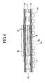
- FIG. 4 is a cross-sectional view of the semiconductor device according to the third embodiment of the present invention.
- parts that are the same as the parts shown in FIG. 2 are given the same reference numerals, and descriptions thereof will be omitted.
- the semiconductor device according to the third embodiment of the present invention has a structure in which the semiconductor chip 3 c is mounted on the top surface of the interposer 1 a of the semiconductor device shown in FIG. 2.
- the semiconductor chip 3 c is electrically connected to the top surface of the interposer 1 a through bumps 8 .
- the semiconductor chip 3 c and the interposer 1 a are bonded by the under-fill adhesive 9 .
- the semiconductor chip 3 b is electrically connected to the top surface of the interposer 1 b through the bumps 8 .
- the interposers 1 a and 1 b are electrically connected by the solder balls 7 , and the solder balls 7 A as external connection terminals are provided on the undersurface of the interposer 1 b . Therefore, the semiconductor chips 3 b and 3 c are electrically connected to the interposer 1 b through the solder balls 7 , and are electrically connectable to an external circuit through the solder balls 7 A serving as external connection terminals.
- the semiconductor device according to the present embodiment can provide the same effect as the semiconductor device according to the above-mentioned first embodiment. Moreover, a heat from the semiconductor chip 3 c , which is stacked on the interposer 1 a , can be transmitted to the lower interposer 1 b through the semiconductor chip 3 a mounted on the undersurface of the interposer 1 a and the semiconductor chip 3 b bonded to the semiconductor chip 3 a . Thereby, the heat from the semiconductor chip 3 c , which is mounted on the top surface of the interposer 1 a , can be efficiently released outside through the interposer 1 b.
- FIG. 5 is a cross-sectional view of the semiconductor device according to the fourth embodiment of the present invention.
- parts that are the same as the parts shown in FIG. 2 are given the same reference numerals, and descriptions thereof will be omitted.
- the semiconductor device has a structure in which a heat spreader 13 is provided on the top surface of the interposer 1 a of the semiconductor device shown in FIG. 2.
- the heat spreader 13 for heat dissipation is formed as a metal layer formed of a material containing Cu, CuW, W, Al, AlC, Ag, etc., and is a member in the form of a sheet or a foil so as to be applied onto the top surface of the interposer 1 a .
- the heat spreader 13 may be formed on the top surface of the interposer by using a wiring material such as a copper foil.
- the heat from the semiconductor chip 3 a is transmitted to the semiconductor chip 3 b and also to the heat spreader 13 through the interposer 1 a , and, therefore, the heat from the semiconductor chip 3 a can be efficiently released outside through the heat spreader 13 . Additionally, when an amount of heat generated in the semiconductor chip 3 b is large, the heat from the semiconductor chip 3 b is transmitted to the semiconductor chip 3 a and the interposer 1 a , and, thus, the heat is efficiently emitted outside through the heat spreader 13 .
- the configuration, the method of forming and the method of arranging of the heat spreader are not limited to the specific configuration and methods, and appropriate configuration and methods may be used if necessary.
- FIG. 6 is a cross-sectional view of the semiconductor device according to the fifth embodiment of the present invention.
- parts that are the same as the parts shown in FIG. 3 are given the same reference numerals, and descriptions thereof will be omitted.
- the semiconductor device according to the fifth embodiment of the present invention has a basic structure the same as that of the semiconductor device according to the second embodiment shown in FIG. 3, and is further provided with a semiconductor chip 3 f .
- the semiconductor chip 3 f is electrically connected to the undersurface of the interposer 1 b through the bumps 8 .
- the semiconductor chip 3 f and the interposer 1 b are bonded by the under-fill adhesive 9 .
- solder ball 7 A as external connection terminals are arranged in the circumference part of the interposer 1 b , and the semiconductor chip 3 f is mounted in the center portion of the under surface of the interposer 1 b by flip-chip bonding. Therefore, solder balls 7 A are formed so that they have a height larger than the height of the semiconductor chip 3 f . According to the present embodiment, the number of stacked semiconductor chips can be increased, and, thus, the package density of semiconductor chips can be improved.
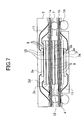
- FIG. 7 is a cross-sectional view of the semiconductor device according to the sixth embodiment of the present invention.
- parts that are the same as the parts shown in FIG. 6 are given the same reference numerals, and descriptions thereof will be omitted.
- the semiconductor device according to the sixth embodiment of the present invention has the same basic structure as the semiconductor device according to the fifth embodiment shown in FIG. 6, and is further provided with a semiconductor chip 3 g .
- the semiconductor chip 3 g is electrically connected to the undersurface of the interposer 1 b through the Au wires 11 .
- the semiconductor chip 3 g is bonded to the back surface of the semiconductor chip 3 f by the die bonding adhesive 10 . Additionally, since the semiconductor chip 3 g is connected by Au wires, the semiconductor chips 3 f and 3 g are integrally encapsulated by the seal resin 2 on the undersurface of the interposer 1 b.
- the solder balls 7 A as external connection terminals are arranged in the circumference part of the interposer 1 b , and the semiconductor chips 3 f and 3 g are stacked and mounted on the center portion of the undersurface of the interposer 1 b by flip-chip bonding. Therefore, the solder balls 7 A are formed so that they have a height larger than the height of the seal resin 2 . According to the present embodiment, the number of stacked semiconductor chips can be increased, and a packaging density of semiconductor chips can be improved.
- FIG. 8 is a cross-sectional view of the semiconductor device according to the seventh embodiment of the present invention.
- parts that are the same as the parts shown in FIG. 3 are given the same reference numerals, and descriptions thereof will be omitted.
- the semiconductor device according to the seventh embodiment of the present invention has a basic structure the same as the semiconductor device according to the second embodiment shown in FIG. 3, and is made as a land-grid-array (LGA) type semiconductor device. That is, although the semiconductor device according to the second embodiment shown in FIG. 3 is a ball-grid-array (BGA) type semiconductor device in which the solder balls 7 A are provided on the undersurface of the interposer, the solder balls are not provided in the present embodiment and electrode pads 14 are exposed on the undersurface of the interposer 1 b so that the electrode pads serve as external connection terminals.
- BGA ball-grid-array
- FIG. 9 is a cross-sectional view of the semiconductor device according to the eighth embodiment of the present invention.
- parts that are the same as the parts shown in FIG. 6 are given the same reference numerals, and descriptions thereof will be omitted.
- the semiconductor device according to the eighth embodiment of the present invention has a basic structure the same as the semiconductor device according to the fifth embodiment shown in FIG. 6, and is configured as a lead-terminal type semiconductor device.
- the semiconductor device according to the fifth embodiment shown in FIG. 6 is a semiconductor device of the BGA (ball grid array) type in which the solder balls 7 A are provided on the undersurface of the interposer so as to serve as external connection terminals
- the semiconductor device according to the present embodiment is not provided with the solder balls 7 A, and, instead, leads 15 are provided on the undersurface of the interposer 1 b so as to serve as external connection terminals.
- FIG. 10 is a cross-sectional view of the semiconductor device according to the ninth embodiment of the present invention.
- parts that are the same as the parts shown in FIG. 3 are given the same reference numerals, and descriptions thereof will be omitted.
- the semiconductor device according to the ninth embodiment of the present invention has a basic structure the same as the semiconductor device according to the second embodiment shown in FIG. 3, and is further provided with interposers 1 c and 1 d .
- Semiconductor chips and solder balls are provided between the interposers 1 b and 1 c and between the interposers 1 c and 1 d in the same arrangement as the structure having the semiconductor chips 3 a and 3 b provided between the interposers 1 a and 1 b .
- the solder balls 7 A serving as external connection terminals are provided on the undersurface of the lowermost interposer 1 d.
- the number of the stacked semiconductor chips can be increased, and the packaging density of the semiconductor chips can be improved.
- the number of interposers and the number of semiconductor chips to be stacked are not limited to the illustrated number, and the number of semiconductor chips can be increased by increasing the number of interposers to be stacked.
- FIG. 11 is a cross-sectional view of the semiconductor device according to the tenth embodiment of the present invention.
- parts that are the same as the parts shown in FIG. 3 are given the same reference numerals, and descriptions thereof will be omitted.
- the semiconductor device according to the tenth embodiment of the present invention has a basic structure the same as the semiconductor device according to the second embodiment shown in FIG. 3, and the connection parts of the solder balls 7 are reinforced by an adhesive 16 . That is, after connecting the interposers 1 a and 1 b mutually with the solder balls 7 , the adhesive 16 is applied around the solder balls 7 and is cured.
- an insulating resin material such as epoxy, acrylics or polyimide is used, and it is preferable to use a thermosetting type resin.
- connection parts of the solder balls 7 are reinforced by the adhesive 16 , the reliability of the connection parts is improved. Additionally, since the solder balls 7 are covered and protected by the adhesive 16 , an electric short-circuit is prevented from occurring between the adjacent solder balls 7 even if, for example, a conductive foreign matter or the like enters between the interposers.
- FIG. 12 is a cross-sectional view of a semiconductor device, which is a variation of the semiconductor device shown in FIG. 11.
- an adhesive 16 A in the form of a sheet or a film is applied on the connection parts of the solder balls 7 instead of applying the adhesive 16 , which is a liquid type, and the adhesive 16 A is cured by heat.
- FIGS. 13A and 13B are illustrations showing examples of the configuration of the adhesive 16 A in the form of a sheet or a film.
- the adhesive 16 A may be formed by a adhesive film having a stripe shape corresponding to the row of the solder balls 7 , as shown in FIG. 13A, and openings 6 Aa are formed beforehand in positions corresponding to the solder balls by punching using a die.
- the adhesive film 16 A may be formed in the shape of a frame, as shown in FIG. 13B, and the openings 16 Aa are formed in positions corresponding to the solder balls 7 .
- the adhesive 16 A may be placed before the solder balls 7 are subjected to reflow so that the adhesive 16 A is melted and cured by the heat of the reflow.
- FIG. 14 is a cross-sectional view of the semiconductor device according to the eleventh embodiment of the present invention.
- parts that are the same as the parts shown in FIG. 2 are given the same reference numerals, and descriptions thereof will be omitted.
- the semiconductor device according to the eleventh embodiment of the present invention differs from the semiconductor device according to the first embodiment shown n FIG. 2 in that only the semiconductor chip 3 b is provided between the interposers 1 a and 1 b and the semiconductor chip 3 c is mounted on the top surface of the upper interposer 1 a.
- semiconductor chip 3 b is mounted by flip-chip connection onto the lower interposer 1 b
- the semiconductor chip 3 c is mounted by flip-chip connection onto the top surface of the upper interposer 1 a . Therefore, the back surface of the semiconductor chip 3 b faces the under surface of the upper interposer 1 a , and the back surface of the semiconductor chip 3 b is bonded to the under surface of the upper interposer 1 a by the adhesive 12 .
- the solder balls 7 extend through inside of the through holes formed in the upper interposer 1 a , and are connected to ball pads 5 a of the top surface of the upper interposer 1 a and ball pads 5 b formed on the top surface of the lower interposer 1 b.
- the adhesive 12 can be cured by heating at the time of reflow by making the adhesive 12 into a fast curable thermosetting resin. Since the adhesive 12 is cured before the solder balls 7 are melted and solidified again, the interposers 1 a and 1 b are fixed to each other when the solder balls are solidified, and, thus, the positions of connection of the solder balls 7 do not shift. Therefore, accurate positioning of is attained and it is prevented that a residual stress occurs in the solder balls 7 at the time of reflow.
- the interposer 1 a since the interposer 1 a is bonded to the semiconductor chip 3 b by the thin layer of the adhesive 12 , the heat generated within the semiconductor chip 3 c is transmitted also to the lower interposer 1 b through the interposer 1 a , the adhesive bond 12 and the semiconductor chip 3 b .
- the heat in the interposer 1 b is efficiently released outside through the solder balls 7 A. Therefore, since the number of paths to transmit the heat from the semiconductor chip mounted on the upper interposer 1 a to the lower interposer 1 b increases according to the present embodiment, the heat from the semiconductor chip can be efficiently released outside through the interposer 1 b.
- the semiconductor chips 3 b and 3 c are mounted on the interposers 1 a and 1 b by flip-chip connection, respectively, a TAB (tape automated bonding technique) may be used as a method of face-down mounting.
- a TAB tape automated bonding technique
- the interposers 1 a and 1 b are electrically connected to each other by the solder balls 7 , the connection is not limited to the disclosed method.
- the interposers 1 a and 1 b may be connected using materials such as a copper post electrode or a resin ball having a surface covered with a conductive material such as a Ni or Au film.
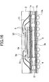
- FIG. 16 is a cross-sectional view of the semiconductor device according to the twelfth embodiment of the present invention.
- parts that are the same as the parts shown in FIG. 14 are given the same reference numerals, and descriptions thereof will be omitted.
- the semiconductor device according to the twelfth embodiment of the present invention is formed by stacking a plurality of semiconductor chips 3 c , 3 d and 3 e on the top surface of the interposer 1 a of the semiconductor device shown in FIG. 14.
- the semiconductor chip 3 c is electrically connected to the top surface of the interposer 1 a through the bumps 8 .
- the semiconductor chip 3 c and the interposer 1 a are bonded by the under-fill adhesive 9 .
- the semiconductor chip 3 d is mounted onto the back surface of the semiconductor chip 3 c , and is bonded to the semiconductor chip 3 c by the die bonding adhesive 10 .
- the die bonding adhesive 10 a resin material such as epoxy, acrylics or polyimide is used.
- the semiconductor chips 3 d is mounted on the semiconductor chip 3 c with the circuit forming surface up, and is electrically connected to electrode pads formed on the top surface of the interposer 1 a by Au wires 11 .
- the semiconductor chip 3 e is smaller than the semiconductor chip 3 d , and is arranged and stacked in the center section of the circuit forming surface of the semiconductor chip 3 d in which no electrode pad is formed.
- the semiconductor chip 3 e is stacked and mounted on the semiconductor chip 3 d with the circuit forming surface up, and is electrically connected to the electrode pads formed on the top surface of the interposer 1 a by the Au wires 11 .
- the semiconductor chips 3 c , 3 d and 3 e are encapsulated by the seal resin 2 on the top surface of the interposer 1 a .
- the seal resin 2 materials such as epoxy, acrylics or polyimide is used.
- the semiconductor device according to the present embodiment can provide the same effect as the semiconductor device according to the above-mentioned eleventh embodiment of the present invention. Moreover, the heat from the semiconductor chips 3 c , 3 d and 3 e stacked on the top surface of the interposer 1 a is transmitted to the lower interposer 1 b through the semiconductor chip 3 b bonded to the top surface of the interposer 1 a . Thereby, the heat from the semiconductor chips 3 c , 3 d and 3 e stacked and mounted on the top surface of the interposer 1 a can also be efficiently released outside through the lower interposer 1 b.
- the present invention is not limited to the number of semiconductor chips and the method of mounting semiconductor chips as explained and a different number of semiconductor chips may be stacked and mounted by a different mounting method.
- connection parts of the solder balls 7 may be reinforced by applying the adhesive 16 or 16 A shown in FIG. 11 or FIG. 12 to the connection parts of the solder balls 7 having the structure shown in FIG. 14.
- the structure shown in FIG. 16 is used as a basic structure and features shown in FIG. 6 through FIG. 10 may be added.
Abstract
A stacked-type semiconductor device has a reduced overall height and an improved reliability in the mechanical strength of the stacked structure. The semiconductor device also has an improved heat release characteristic. A first interposer has a surface on which first electrode pads are formed and a first semiconductor element is mounted with a circuit forming surface facing the first interposer. A second interposer has a surface on which second electrode pads are formed and a second semiconductor element is mounted with a circuit forming surface facing the second interposer. External connection terminals are provided on a surface of the second interposer opposite to the surface on which the second semiconductor element is mounted. The first and second interposers are electrically connected to each other by conductive members provided therebetween. A back surface of the first semiconductor element and a back surface of the second semiconductor element are fixed to each other by an adhesive.
Description
- 1. Field of the Invention
- The present invention generally relates to semiconductor devices and, more particularly, to a semiconductor device having a three-dimensional structure in which a plurality of semiconductor devices and semiconductor elements are stacked, and a manufacturing method of such a semiconductor device.
- With the development of electric equipments in recent years, a demand for miniaturization in dimensions and thickness, multifunction, high-performance and high-density in the semiconductor devices has been increasing. In order to cope with such a demand, the structure of the semiconductor devices has been shifting to a three-dimensional structure in which a plurality of semiconductor devices or a plurality of semiconductor elements are stacked.
- 2. Description of the Related Art
- Japanese Laid-Open Patent Application No. 2001-223297 discloses an example of a semiconductor device, which has a three-dimensional structure formed by stacking a plurality of semiconductor devices. FIG. 1 is a cross-sectional view of the semiconductor device disclosed in the above-mentioned patent document.
- In FIG. 1,
semiconductor chips 3 are mounted on both sides of each ofinterposers 1, and are encapsulated by aseal resin 2, respectively. The twointerposers 1 are stacked with theseal resin 2, which encapsulates thesemiconductor chip 3, interposed therebetween. Theinterposers 1 are connected to each other by bondingsolder balls 7 toball pads 5 which are exposed in throughholes 6 formed in asolder resist 4. That is, the upper andlower interposers 1 are electrically connected to each other by thesolder balls 7, and are also connect mechanically to each other. - In the semiconductor device shown in FIG. 1, since each semiconductor chip mounted on the stacked interposers is encapsulated by the seal resin, it is necessary to provide a distance between two interposers, which distance is greater than the thickness of the seal resin layer interposed between two interposers. Therefore, if the distance between the interposers can be reduced, the overall height of the semiconductor device can also be reduced.
- Additionally, since the interposers are connected and fixed to each other by the solder balls provided in the peripheral portion of the interposers, if a warp occurs in the interposers in a stacking process of an assembling process of the semiconductor package, a defect may occur in the connecting part between the interposers. Moreover, when mounting the complete semiconductor package onto a substrate, a defect may occur in the connecting part between the interposers due to a thermal deformation of the interposers and remelting of the solder balls.
- Furthermore, since the complete semiconductor package is mechanically connected by a small area with only the solder balls, a stress tends to be concentrated into the connecting part between the interposers, which may deteriorate mechanical reliability of the package.
- It is a general object of the present invention to provide an improved and useful semiconductor device in which the above-mentioned problems are eliminated.
- A more specific object of the present invention is to provide a semiconductor device having a three-dimensional structure in which a plurality of semiconductor devices or a plurality of semiconductor elements are stacked, the semiconductor device having a reduced overall height and an improved reliability in the mechanical strength of the stacked structure.
- Another object of the present invention is to provide a semiconductor device having a three-dimensional structure in which a plurality of semiconductor devices or a plurality of semiconductor elements are stacked, the semiconductor device having an improved heat release characteristic.
- In order to achieve the above-mentioned objects, there is provided according to one aspect of the present invention a semiconductor device comprising: a first semiconductor element having a circuit forming surface and a back surface opposite to the circuit forming surface; a first interposer having a surface on which first electrode pads are formed and the first semiconductor element is mounted with the circuit forming surface facing the first interposer; a second semiconductor element having a circuit forming surface and a back surface opposite to the circuit forming surface; a second interposer having a surface on which second electrode pads are formed and the second semiconductor element is mounted with the circuit forming surface facing the second interposer, the second electrode pads for connection with the first interposer; and external connection terminals provided on a surface of the second interposer opposite to the surface on which the second semiconductor element is mounted, wherein the first interposer and the second interposer are electrically connected to each other by conductive members between the first and second electrode pads, and the back surface of the first semiconductor element and the back surface of the second semiconductor element are fixed to each other by an adhesive.
- According to the above-mentioned invention, there is no need to encapsulate the first and second semiconductor elements provided between the first and second interposers. Thus, a distance between the first and second interposers can be reduced, which results in a reduction in an overall thickness of the semiconductor device. Additionally, since the first and second semiconductor elements are bonded to each other by the adhesive, a mechanical strength of the connection between the interposers is improved, which prevents warp of the interposers. Further, since the first and second semiconductor elements are bonded to each other by the adhesive, a heat generated in the first semiconductor element can be efficiently released outside through the second semiconductor element and the second interposer.
- The semiconductor device according to the present invention may further comprise at least one third semiconductor element which is mounted on a surface of the first interposer opposite to the surface on which the first semiconductor element is mounted. Accordingly, the number of semiconductor elements stacked in the semiconductor device can be increased, which improves a packaging density. Additionally, a plurality of the third semiconductor elements may be mounted and encapsulated on the surface of the first interposer in a stacked and fixed state. Accordingly, semiconductor elements of different kinds or sizes can be efficiently arranged within the semiconductor device. Further, a metal layer for heat release may be provided on a surface of the first interposer opposite to the surface on which the first semiconductor element is mounted. Accordingly, the metal layer serves as a heat spreader, which can efficiently release a heat of the semiconductor elements to outside of the semiconductor device.
- Additionally, there is provided according to another aspect of the present invention a semiconductor device comprising: a first semiconductor element having a circuit forming surface and a back surface opposite to the circuit forming surface; a first interposer having a surface on which first electrode pads are formed and the first semiconductor element is mounted with the circuit forming surface facing the first interposer; a second semiconductor element having a circuit forming surface and a back surface opposite to the circuit forming surface; a second interposer having a surface on which second electrode pads are formed and the second semiconductor element is mounted with the circuit forming surface facing the second interposer, the second electrode pads for connection with the first interposer; and external connection terminals provided on a surface of the second interposer opposite to the surface on which the second semiconductor element is mounted, wherein the first interposer and the second interposer are electrically connected to each other by conductive members between the first and second electrode pads, and the first interposer and the back surface of the second semiconductor element are fixed to each other by an adhesive.
- According to the above-mentioned invention, there is no need to encapsulate the second semiconductor element provided between the first and second interposers. Thus, a distance between the first and second interposers can be reduced, which results in a reduction in an overall thickness of the semiconductor device. Additionally, since the second semiconductor element and the first interposer are bonded to each other by the adhesive, a mechanical strength of the connection between the interposers is improved, which prevents warp of the interposers. Further, since the second semiconductor element is bonded to the first interposer by the adhesive, a heat generated in the first semiconductor element can be efficiently released outside through the first interposer, the second semiconductor element and the second interposer.
- The semiconductor device according to the present invention may further comprise at least one third semiconductor element mounted on the surface of the first interposer on which the first semiconductor element is mounted. Accordingly, the number of semiconductor elements stacked in the semiconductor device can be increased, which improves a packaging density. Additionally, the semiconductor device may further comprise at least one third semiconductor element is stacked on the first semiconductor element, and the first and third semiconductor elements may be encapsulated on the first interposer.
- Additionally, in the semiconductor device according to the present invention, at least one fourth semiconductor element may be mounted on the surface of the second interposer provided with the external connection terminals. A plurality of the fourth semiconductor elements may be provided and encapsulated on the second interposer.
- Further, each of the external connection terminals may be a flat pad, or may have a protruding shape. Each of the external connection terminals may be a lead terminal extending in a direction outward from the second interposer.
- Additionally, the adhesive, which bonds the back surface of the first semiconductor element and the back surface of the second semiconductor element to each other, may be a thermosetting type resin adhesive. The thermosetting type resin adhesive may contain at least one of silver and copper.
- Further, in the semiconductor device according to the present invention, a reinforcing adhesive may be provided to connecting parts between the conductive materials and the first and second interposers. The reinforcing adhesive may be made of an insulating thermosetting type resin material. The reinforcing adhesive may be in the form of a film having openings corresponding to positions of the conductive members.
- Additionally, there is provided according to another aspect of the present invention a manufacturing method of a semiconductor device comprising a first semiconductor element and a second semiconductor element, comprising the steps of: mounting the first semiconductor element onto a first interposer in a state in which a circuit forming surface of the first semiconductor element faces the first interposer; mounting the second semiconductor element onto a second interposer in a state in which a circuit forming surface of the second semiconductor element faces the second interposer; electrically connecting the first interposer and the second interposer to each other by stacking the first and second interposers with the second semiconductor element interposed therebetween and heating conductive members provided between the first and second interposers so as to melt the conductive members; and curing a thermosetting adhesive provided between a back surface of the second semiconductor device and one of a back surface of the first semiconductor element and the first interposer by a heat in the step of electrically connecting.
- Other objects, features and advantages of the present invention will become more apparent from the following detailed description when read in conjunction with the accompanying drawings.
- FIG. 1 is a cross-sectional view of a conventional semiconductor device;
- FIG. 2 is a cross-sectional view of a semiconductor device according to a first embodiment of the present invention;
- FIG. 3 is a cross-sectional view of a semiconductor device according to a second embodiment of the present invention;
- FIG. 4 is a cross-sectional view of a semiconductor device according to a third embodiment of the present invention;
- FIG. 5 is a cross-sectional view of a semiconductor device according to a fourth embodiment of the present invention;
- FIG. 6 is a cross-sectional view of a semiconductor device according to a fifth embodiment of the present invention;
- FIG. 7 is a cross-sectional view of a semiconductor device according to a sixth embodiment of the present invention;
- FIG. 8 is a cross-sectional view of a semiconductor device according to a seventh embodiment of the present invention;
- FIG. 9 is a cross-sectional view of a semiconductor device according to an eight embodiment of the present invention;
- FIG. 10 is a cross-sectional view of a semiconductor device according to a ninth embodiment of the present invention;
- FIG. 11 is a cross-sectional view of a semiconductor device according to a tenth embodiment of the present invention;
- FIG. 12 is a cross-sectional view of a semiconductor device, which is a variation of the semiconductor device shown in FIG. 11;
- FIGS. 13A and 13B are illustrations of configurations of an adhesive shown in FIG. 11;
- FIG. 14 is a cross-sectional view of a semiconductor device according to an eleventh embodiment of the present invention;
- FIG. 15 is a cross-sectional view of a semiconductor device, which is a variation of the semiconductor device shown in FIG. 14; and
- FIG. 16 is a cross-sectional view of a semiconductor device according to a twelfth embodiment of the present invention.
- A description will now be given, with reference to FIG. 2, of a semiconductor device according to a first embodiment of the present invention. FIG. 2 is a cross-sectional view of the semiconductor device according to the first embodiment of the present invention.
- The semiconductor device shown in FIG. 2 has a configuration where an
interposer 1 a on which asemiconductor chip 3 a is mounted and aninterposer 1 b on which asemiconductor chip 3 b is mounted are stacked. Theinterposer 1 a and theinterposer 1 b are rearranging substrates, and are formed of a polyimide tape substrate, a glass epoxy substrate, an organic substrate (polycarbonate), etc. Theinterposer 1 a and theinterposer 1 b are electrically connected to each other bysolder balls 7, which are conductive members. - The
semiconductor chip 3 a is mounted onto theinterposer 1 a by flip-chip-bonding, which is generally referred to as face-down mounting. That is, thesemiconductor chip 3 a is electrically connected to electrode pads formed on the undersurface of theinterposer 1 a throughbumps 8 provided on the circuit forming surface of thesemiconductor chip 3. Thebumps 8 are formed of gold, copper, solder, polymer, etc. Thesemiconductor chip 3 a and theinterposer 1 a are bonded by an under-fill adhesive 9 provided therebetween so as to be fixed to each other. As for the under-fill adhesive 9, a resin material such as epoxy, acrylics or polyimide is used. - Similarly, the
semiconductor chip 3 b is mounted on theinterposer 1 b by face-down mounting (flip-chip-bonding). That is, thesemiconductor chip 3 b is electrically connected to electrode pads formed on the top surface of theinterposer 1 b through thebumps 8 provided on the circuit forming surface of thesemiconductor chip 3 b. Thesemiconductor chip 3 b and theinterposer 1 b are bonded by the under-fill adhesive 9 provided therebetween, and are fixed to each other. - The
interposer 1 a and theinterposer 1 b are stacked with thesemiconductor chips semiconductor chips semiconductor chips semiconductor chips -
Solder balls 7A are provided as external connection terminals on the under surface of thelower interposer 1 b, and parts other than the part in which thesolder balls 7A are provided are covered by a solder resist 4. - The
solder balls 7, which electrically connectinterposer 1 a and theinterposer 1 b, are joined to bothball pads 5 a formed on the undersurface of theinterposer 1 a andball pads 5 b formed on the top surface of theinterposer 1 b. Therefore, the height of thesolder balls 7 is almost equal to a height of a sum of the heights of thesemiconductor chip 3 a and thesemiconductor chip 3 b. Theball pads 5 a and theball pad 5 b are formed as parts exposed in openings formed in the solder resist 4. - Here, since the circuit forming surface of the
semiconductor chip 3 a faces theinterposer 1 a and the under-fill adhesive 9 is filled therebetween, there is no need to encapsulate thesemiconductor chip 3 a by a seal resin. Similarly, since the circuit forming surface of thesemiconductor chip 3 b faces theinterposer 1 b and the under-fill adhesive 9 is filled therebetween, there is no need to encapsulate thesemiconductor chip 3 b by a seal resin. - Therefore, there is no need to maintain a height (distance) which is required for the seal resin part between the
interposer 1 a and theinterposer 1 b, and only a distance corresponding to a sum of the heights of thesemiconductor chips - Additionally, the
interposer 1 a and theinterposer 1 b are mechanically and firmly bonded by bonding thesemiconductor chip 3 a and thesemiconductor chip 3 b with the adhesive 12 in addition to the connection by thesolder balls 7. Therefore, a thermal stress and an external force are prevented from concentrating into the connection parts of thesolder balls 7, thereby improving the reliability of the mechanical connection between the interposers. - Furthermore, by making the
adhesive bond 12 as a fast cure type thermosetting resin, the adhesive 12 can be cured by heating during a reflow process to join thesolder balls 7 to theinterposers solder balls 7 melt and solidify again, theinterposer 1 a and theinterposer 1 b are fixed to each other when thesolder balls 7 are cured, and, thus, the connecting positions of the solder balls cannot shift. Therefore, an accurate positioning can be achieved, and generation of a residual stress in the solder balls in the reflow process can be prevented. - Moreover, in the present embodiment, since the
semiconductor chip 3 a is bonded to thesemiconductor chip 3 b by the thin layer of an adhesive 12, the heat generated within thesemiconductor chip 3 a is transmitted also to thelower interposer 1 b through theadhesive bond 12 and thesemiconductor chip 3 b. The heat of theinterposer 1 b is efficiently emitted outside through thesolder balls 7A. Therefore, according to the present embodiment, since a number of paths to transmit a heat from the semiconductor chip mounted on theupper interposer 1 a to thelower interposer 1 b is increased, the heat from the semiconductor chip can be efficiently released outside through theinterposer 1 b. - It should be noted that although the
semiconductor chips respective interposers interposers solder balls 7, the bonding material and method are not limited to that disclosed. For example, instead of thesolder balls 7, the connection can be made by copper post electrodes or resin balls having surfaces covered by a conductive material such as Ni/Au and the like. - Next, a description will be given, with reference to FIG. 3, of a semiconductor device according to a second embodiment of the present invention. FIG. 3 is a cross-sectional view of the semiconductor device according to the second embodiment of the present invention. In FIG. 3, parts that are the same as the parts shown in FIG. 2 are given the same reference numerals, and descriptions thereof will be omitted.
- The semiconductor device according to the second embodiment of the present invention is configured by mounting a plurality of
semiconductor chips - The
semiconductor chip 3 c is electrically connected to the top surface of theinterposer 1 a through bumps 8. Thesemiconductor chip 3 c and theinterposer 1 a are bonded by the under-fill adhesive 9. - The
semiconductor chip 3 d is mounted on the back surface of thesemiconductor chip 3 c in a stacked state, and is bonded to thesemiconductor chip 3 c by a die-bonding adhesive 10. As for the die-bonding adhesive 10, a resin material such as epoxy, acrylics or polyimide can be used. Thesemiconductor chip 3 d is mounted on thesemiconductor chip 3 c with the circuit forming surface up, and is electrically connected to the electrode pads formed on the top surface of theinterposer 1 a by Au wires. - The
semiconductor chip 3 e is smaller than thesemiconductor chip 3 d, and is arranged in a stacked state in the center portion of the circuit forming surface of thesemiconductor chip 3 d where no electrode pad is formed. Thesemiconductor chip 3 e is stacked on thesemiconductor chip 3 d with the circuit forming surface up, and is electrically connected to the electrode pads formed on the top surface of theinterposer 1 a by Au wires. - In the above-mentioned structure, the
semiconductor chips seal resin 2 on the top surface of theinterposer 1 a. As for theseal resin 2, materials such as epoxy, acrylics or polyimide can be used. - The semiconductor device according to the present embodiment can provide the same effects as the semiconductor device according to the above-mentioned first embodiment. Additionally, a heat from the
semiconductor chips interposer 1 a, is also transmitted to thelower interposer 1 b through thesemiconductor chip 3 a and thesemiconductor chip 3 b bonded to thesemiconductor chip 3 a. Thereby, the heat from thesemiconductor chips interposer 1 a, can also be efficiently emitted outside through thelower interposer 1 b. - It should be noted that, although three semiconductor chips are stacked on the
interposer 1 a and encapsulated by a seal resin, the present invention is not limited to the number of semiconductor chips and the method of mounting, and a different number of semiconductor chips may be mounted by a different mounting method. - Next, a description will be given, with reference to FIG. 4, of a semiconductor device according to a third embodiment of the present invention. FIG. 4 is a cross-sectional view of the semiconductor device according to the third embodiment of the present invention. In FIG. 4, parts that are the same as the parts shown in FIG. 2 are given the same reference numerals, and descriptions thereof will be omitted.
- The semiconductor device according to the third embodiment of the present invention has a structure in which the
semiconductor chip 3 c is mounted on the top surface of theinterposer 1 a of the semiconductor device shown in FIG. 2. Thesemiconductor chip 3 c is electrically connected to the top surface of theinterposer 1 a through bumps 8. Thesemiconductor chip 3 c and theinterposer 1 a are bonded by the under-fill adhesive 9. - Since the
semiconductor chip 3 c stacked on theinterposer 1 a is mounted with the circuit forming surface down and the under-fill adhesive 9 is filled between the circuit forming surface and theinterposer 1 a, there is no need to encapsulate thesemiconductor chip 3 c by a seal resin. - As mentioned above, the
semiconductor chip 3 b is electrically connected to the top surface of theinterposer 1 b through thebumps 8. Moreover, theinterposers solder balls 7, and thesolder balls 7A as external connection terminals are provided on the undersurface of theinterposer 1 b. Therefore, thesemiconductor chips interposer 1 b through thesolder balls 7, and are electrically connectable to an external circuit through thesolder balls 7A serving as external connection terminals. - The semiconductor device according to the present embodiment can provide the same effect as the semiconductor device according to the above-mentioned first embodiment. Moreover, a heat from the
semiconductor chip 3 c, which is stacked on theinterposer 1 a, can be transmitted to thelower interposer 1 b through thesemiconductor chip 3 a mounted on the undersurface of theinterposer 1 a and thesemiconductor chip 3 b bonded to thesemiconductor chip 3 a. Thereby, the heat from thesemiconductor chip 3 c, which is mounted on the top surface of theinterposer 1 a, can be efficiently released outside through theinterposer 1 b. - Next, a description will be given, with reference to FIG. 5, of a semiconductor device according to a fourth embodiment of the present invention. FIG. 5 is a cross-sectional view of the semiconductor device according to the fourth embodiment of the present invention. In FIG. 5, parts that are the same as the parts shown in FIG. 2 are given the same reference numerals, and descriptions thereof will be omitted.
- The semiconductor device according to the fourth embodiment of the present invention has a structure in which a
heat spreader 13 is provided on the top surface of theinterposer 1 a of the semiconductor device shown in FIG. 2. Theheat spreader 13 for heat dissipation is formed as a metal layer formed of a material containing Cu, CuW, W, Al, AlC, Ag, etc., and is a member in the form of a sheet or a foil so as to be applied onto the top surface of theinterposer 1 a. When producing theheat spreader 13, theheat spreader 13 may be formed on the top surface of the interposer by using a wiring material such as a copper foil. - In the present embodiment, the heat from the
semiconductor chip 3 a is transmitted to thesemiconductor chip 3 b and also to theheat spreader 13 through theinterposer 1 a, and, therefore, the heat from thesemiconductor chip 3 a can be efficiently released outside through theheat spreader 13. Additionally, when an amount of heat generated in thesemiconductor chip 3 b is large, the heat from thesemiconductor chip 3 b is transmitted to thesemiconductor chip 3 a and theinterposer 1 a, and, thus, the heat is efficiently emitted outside through theheat spreader 13. - It should be noted that the configuration, the method of forming and the method of arranging of the heat spreader are not limited to the specific configuration and methods, and appropriate configuration and methods may be used if necessary.
- Next, a description will be given, with reference to FIG. 6, of a semiconductor device according to a fifth embodiment of the present invention. FIG. 6 is a cross-sectional view of the semiconductor device according to the fifth embodiment of the present invention. In FIG. 6, parts that are the same as the parts shown in FIG. 3 are given the same reference numerals, and descriptions thereof will be omitted.
- The semiconductor device according to the fifth embodiment of the present invention has a basic structure the same as that of the semiconductor device according to the second embodiment shown in FIG. 3, and is further provided with a
semiconductor chip 3 f. Thesemiconductor chip 3 f is electrically connected to the undersurface of theinterposer 1 b through thebumps 8. Thesemiconductor chip 3 f and theinterposer 1 b are bonded by the under-fill adhesive 9. - In the present embodiment, the
solder ball 7A as external connection terminals are arranged in the circumference part of theinterposer 1 b, and thesemiconductor chip 3 f is mounted in the center portion of the under surface of theinterposer 1 b by flip-chip bonding. Therefore,solder balls 7A are formed so that they have a height larger than the height of thesemiconductor chip 3 f. According to the present embodiment, the number of stacked semiconductor chips can be increased, and, thus, the package density of semiconductor chips can be improved. - Next, a description will be given, with reference to FIG. 7, of a semiconductor device according to a sixth embodiment of the present invention. FIG. 7 is a cross-sectional view of the semiconductor device according to the sixth embodiment of the present invention. In FIG. 7, parts that are the same as the parts shown in FIG. 6 are given the same reference numerals, and descriptions thereof will be omitted.
- The semiconductor device according to the sixth embodiment of the present invention has the same basic structure as the semiconductor device according to the fifth embodiment shown in FIG. 6, and is further provided with a
semiconductor chip 3 g. Thesemiconductor chip 3 g is electrically connected to the undersurface of theinterposer 1 b through theAu wires 11. Thesemiconductor chip 3 g is bonded to the back surface of thesemiconductor chip 3 f by thedie bonding adhesive 10. Additionally, since thesemiconductor chip 3 g is connected by Au wires, thesemiconductor chips seal resin 2 on the undersurface of theinterposer 1 b. - In the present embodiment, the
solder balls 7A as external connection terminals are arranged in the circumference part of theinterposer 1 b, and thesemiconductor chips interposer 1 b by flip-chip bonding. Therefore, thesolder balls 7A are formed so that they have a height larger than the height of theseal resin 2. According to the present embodiment, the number of stacked semiconductor chips can be increased, and a packaging density of semiconductor chips can be improved. - Next, a description will be given, with reference to FIG. 8, of a semiconductor device according to a seventh embodiment of the present invention. FIG. 8 is a cross-sectional view of the semiconductor device according to the seventh embodiment of the present invention. In FIG. 8, parts that are the same as the parts shown in FIG. 3 are given the same reference numerals, and descriptions thereof will be omitted.
- The semiconductor device according to the seventh embodiment of the present invention has a basic structure the same as the semiconductor device according to the second embodiment shown in FIG. 3, and is made as a land-grid-array (LGA) type semiconductor device. That is, although the semiconductor device according to the second embodiment shown in FIG. 3 is a ball-grid-array (BGA) type semiconductor device in which the
solder balls 7A are provided on the undersurface of the interposer, the solder balls are not provided in the present embodiment andelectrode pads 14 are exposed on the undersurface of theinterposer 1 b so that the electrode pads serve as external connection terminals. - Next, a description will be given, with reference to FIG. 9, of a semiconductor device according to an eighth embodiment of the present invention. FIG. 9 is a cross-sectional view of the semiconductor device according to the eighth embodiment of the present invention. In FIG. 9, parts that are the same as the parts shown in FIG. 6 are given the same reference numerals, and descriptions thereof will be omitted.
- The semiconductor device according to the eighth embodiment of the present invention has a basic structure the same as the semiconductor device according to the fifth embodiment shown in FIG. 6, and is configured as a lead-terminal type semiconductor device. Namely, although the semiconductor device according to the fifth embodiment shown in FIG. 6 is a semiconductor device of the BGA (ball grid array) type in which the
solder balls 7A are provided on the undersurface of the interposer so as to serve as external connection terminals, the semiconductor device according to the present embodiment is not provided with thesolder balls 7A, and, instead, leads 15 are provided on the undersurface of theinterposer 1 b so as to serve as external connection terminals. - Next, a description will be given, with reference to FIG. 10, of a semiconductor device according to a ninth embodiment of the present invention. FIG. 10 is a cross-sectional view of the semiconductor device according to the ninth embodiment of the present invention. In FIG. 10, parts that are the same as the parts shown in FIG. 3 are given the same reference numerals, and descriptions thereof will be omitted.
- The semiconductor device according to the ninth embodiment of the present invention has a basic structure the same as the semiconductor device according to the second embodiment shown in FIG. 3, and is further provided with
interposers interposers interposers semiconductor chips interposers solder balls 7A serving as external connection terminals are provided on the undersurface of thelowermost interposer 1 d. - According to the present embodiment, the number of the stacked semiconductor chips can be increased, and the packaging density of the semiconductor chips can be improved. The number of interposers and the number of semiconductor chips to be stacked are not limited to the illustrated number, and the number of semiconductor chips can be increased by increasing the number of interposers to be stacked.
- Next, a description will be given, with reference to FIG. 11, of a semiconductor device according to a tenth embodiment of the present invention. FIG. 11 is a cross-sectional view of the semiconductor device according to the tenth embodiment of the present invention. In FIG. 11, parts that are the same as the parts shown in FIG. 3 are given the same reference numerals, and descriptions thereof will be omitted.
- The semiconductor device according to the tenth embodiment of the present invention has a basic structure the same as the semiconductor device according to the second embodiment shown in FIG. 3, and the connection parts of the
solder balls 7 are reinforced by an adhesive 16. That is, after connecting theinterposers solder balls 7, the adhesive 16 is applied around thesolder balls 7 and is cured. As the adhesive 16, an insulating resin material such as epoxy, acrylics or polyimide is used, and it is preferable to use a thermosetting type resin. - According to the present embodiment, since the connection parts of the
solder balls 7 are reinforced by the adhesive 16, the reliability of the connection parts is improved. Additionally, since thesolder balls 7 are covered and protected by the adhesive 16, an electric short-circuit is prevented from occurring between theadjacent solder balls 7 even if, for example, a conductive foreign matter or the like enters between the interposers. - FIG. 12 is a cross-sectional view of a semiconductor device, which is a variation of the semiconductor device shown in FIG. 11. In the semiconductor device shown in FIG. 12, an adhesive 16A in the form of a sheet or a film is applied on the connection parts of the
solder balls 7 instead of applying the adhesive 16, which is a liquid type, and the adhesive 16A is cured by heat. - FIGS. 13A and 13B are illustrations showing examples of the configuration of the adhesive 16A in the form of a sheet or a film. The adhesive 16A may be formed by a adhesive film having a stripe shape corresponding to the row of the
solder balls 7, as shown in FIG. 13A, and openings 6Aa are formed beforehand in positions corresponding to the solder balls by punching using a die. When thesolder balls 7 are circumferentially arranged, theadhesive film 16A may be formed in the shape of a frame, as shown in FIG. 13B, and the openings 16Aa are formed in positions corresponding to thesolder balls 7. The adhesive 16A may be placed before thesolder balls 7 are subjected to reflow so that the adhesive 16A is melted and cured by the heat of the reflow. - Next, a description will be given, with reference to FIG. 14, of a semiconductor device according to an eleventh embodiment of the present invention. FIG. 14 is a cross-sectional view of the semiconductor device according to the eleventh embodiment of the present invention. In FIG. 14, parts that are the same as the parts shown in FIG. 2 are given the same reference numerals, and descriptions thereof will be omitted.
- The semiconductor device according to the eleventh embodiment of the present invention differs from the semiconductor device according to the first embodiment shown n FIG. 2 in that only the
semiconductor chip 3 b is provided between theinterposers semiconductor chip 3 c is mounted on the top surface of theupper interposer 1 a. - Here,
semiconductor chip 3 b is mounted by flip-chip connection onto thelower interposer 1 b, and thesemiconductor chip 3 c is mounted by flip-chip connection onto the top surface of theupper interposer 1 a. Therefore, the back surface of thesemiconductor chip 3 b faces the under surface of theupper interposer 1 a, and the back surface of thesemiconductor chip 3 b is bonded to the under surface of theupper interposer 1 a by the adhesive 12. Thesolder balls 7 extend through inside of the through holes formed in theupper interposer 1 a, and are connected toball pads 5 a of the top surface of theupper interposer 1 a andball pads 5 b formed on the top surface of thelower interposer 1 b. - In the present embodiment, there is no need to maintain a height (distance) that is required for a resin seal part between the
interposers semiconductor chip 3 b and the thickness of the adhesive 12, may be maintained. Thereby, the thickness of the semiconductor device according to the present embodiment can be reduced. - Additionally, in the present embodiment, since the back surface of the
semiconductor chip 3 b is fixed directly to theupper interposer 1 c by the adhesive 12, similar to the above-mentioned semiconductor device according to the first embodiment shown in FIG. 2, it is prevented that a thermal stress and an external force are concentrated into the connection parts of thesolder balls 7, thereby improving the reliability of the mechanical connection between the interposers. - Furthermore, in the process of joining the
solder balls 7 to theinterposers solder balls 7 are melted and solidified again, theinterposers solder balls 7 do not shift. Therefore, accurate positioning of is attained and it is prevented that a residual stress occurs in thesolder balls 7 at the time of reflow. - Moreover, in the present embodiment, since the
interposer 1 a is bonded to thesemiconductor chip 3 b by the thin layer of the adhesive 12, the heat generated within thesemiconductor chip 3 c is transmitted also to thelower interposer 1 b through theinterposer 1 a, theadhesive bond 12 and thesemiconductor chip 3 b. The heat in theinterposer 1 b is efficiently released outside through thesolder balls 7A. Therefore, since the number of paths to transmit the heat from the semiconductor chip mounted on theupper interposer 1 a to thelower interposer 1 b increases according to the present embodiment, the heat from the semiconductor chip can be efficiently released outside through theinterposer 1 b. - In addition, although the
semiconductor chips interposers interposers solder balls 7, the connection is not limited to the disclosed method. For example, instead of thesolder balls 7, theinterposers - It should be noted that, in the present embodiment, although one
semiconductor chip 3 c is mounted on theupper interposer 1 a, a plurality of thesemiconductor chips 3 c may be mounted on theupper interposer 1 a, as shown in FIG. 15. - Next, a description will be given, with reference to FIG. 16, of a semiconductor device according to a twelfth embodiment of the present invention. FIG. 16 is a cross-sectional view of the semiconductor device according to the twelfth embodiment of the present invention. In FIG. 16, parts that are the same as the parts shown in FIG. 14 are given the same reference numerals, and descriptions thereof will be omitted.
- The semiconductor device according to the twelfth embodiment of the present invention is formed by stacking a plurality of
semiconductor chips interposer 1 a of the semiconductor device shown in FIG. 14. - The
semiconductor chip 3 c is electrically connected to the top surface of theinterposer 1 a through thebumps 8. Thesemiconductor chip 3 c and theinterposer 1 a are bonded by the under-fill adhesive 9. - The
semiconductor chip 3 d is mounted onto the back surface of thesemiconductor chip 3 c, and is bonded to thesemiconductor chip 3 c by thedie bonding adhesive 10. As for thedie bonding adhesive 10, a resin material such as epoxy, acrylics or polyimide is used. The semiconductor chips 3 d is mounted on thesemiconductor chip 3 c with the circuit forming surface up, and is electrically connected to electrode pads formed on the top surface of theinterposer 1 a byAu wires 11. - The
semiconductor chip 3 e is smaller than thesemiconductor chip 3 d, and is arranged and stacked in the center section of the circuit forming surface of thesemiconductor chip 3 d in which no electrode pad is formed. Thesemiconductor chip 3 e is stacked and mounted on thesemiconductor chip 3 d with the circuit forming surface up, and is electrically connected to the electrode pads formed on the top surface of theinterposer 1 a by theAu wires 11. - In the above-mentioned structure, the
semiconductor chips seal resin 2 on the top surface of theinterposer 1 a. As for theseal resin 2, materials such as epoxy, acrylics or polyimide is used. - The semiconductor device according to the present embodiment can provide the same effect as the semiconductor device according to the above-mentioned eleventh embodiment of the present invention. Moreover, the heat from the
semiconductor chips interposer 1 a is transmitted to thelower interposer 1 b through thesemiconductor chip 3 b bonded to the top surface of theinterposer 1 a. Thereby, the heat from thesemiconductor chips interposer 1 a can also be efficiently released outside through thelower interposer 1 b. - It should be noted that although three semiconductor chips are stacked and encapsulated on the top surface of the
interposer 1 a, the present invention is not limited to the number of semiconductor chips and the method of mounting semiconductor chips as explained and a different number of semiconductor chips may be stacked and mounted by a different mounting method. - Although the embodiments of the present invention were explained above, the present invention is not limited to the features disclosed in the above-mentioned embodiments, and it is interpreted that a combination of the above-mentioned embodiments is also within the scope of the present invention. For example, the connection parts of the
solder balls 7 may be reinforced by applying the adhesive 16 or 16A shown in FIG. 11 or FIG. 12 to the connection parts of thesolder balls 7 having the structure shown in FIG. 14. Additionally, the structure shown in FIG. 16 is used as a basic structure and features shown in FIG. 6 through FIG. 10 may be added. - The present invention is not limited to the specifically disclosed embodiments, and variations and modifications may be made without departing from the scope of the present invention.
- The present application is based on Japanese priority application No. 2002-117534 filed Apr. 19, 2002, the entire contents of which are hereby incorporated by reference.
Claims (28)
1. A semiconductor device comprising:
a first semiconductor element having a circuit forming surface and a back surface opposite to the circuit forming surface;
a first interposer having a surface on which first electrode pads are formed and said first semiconductor element is mounted with the circuit forming surface facing the first interposer;
a second semiconductor element having a circuit forming surface and a back surface opposite to the circuit forming surface;
a second interposer having a surface on which second electrode pads are formed and said second semiconductor element is mounted with the circuit forming surface facing the second interposer, the second electrode pads for connection with said first interposer; and
external connection terminals provided on a surface of said second interposer opposite to the surface on which said second semiconductor element is mounted,
wherein said first interposer and said second interposer are electrically connected to each other by conductive members between said first and second electrode pads, and the back surface of said first semiconductor element and the back surface of said second semiconductor element are fixed to each other by an adhesive.
2. The semiconductor device as claimed in claim 1 , further comprising at least one third semiconductor element which is mounted on a surface of said first interposer opposite to the surface on which said first semiconductor element is mounted.
3. The semiconductor device as claimed in claim 2 , wherein a plurality of the third semiconductor elements are mounted and encapsulated on the surface of said first interposer in a stacked and fixed state.
4. The semiconductor device as claimed in claim 1 , wherein a metal layer for heat release is provided on a surface of said first interposer opposite to the surface on which said first semiconductor element is mounted.
5. The semiconductor device as claimed in claim 1 , wherein at least one fourth semiconductor element is mounted on the surface of said second interposer provided with said external connection terminals.
6. The semiconductor device as claimed in claim 5 , wherein a plurality of the fourth semiconductor elements are provided and encapsulated on said second interposer.
7. The semiconductor device as claimed in claim 1 , wherein each of said external connection terminals is a flat pad.
8. The semiconductor device as claimed in claim 1 , wherein each of said external connection terminals has a protruding shape.
9. The semiconductor device as claimed in claim 1 , wherein each of said external connection terminals is a lead terminal extending in a direction outward from said second interposer.
10. The semiconductor device as claimed in claim 1 , wherein said adhesive, which bonds the back surface of said first semiconductor element and the back surface of said second semiconductor element to each other, is a thermosetting type resin adhesive.
11. The semiconductor device as claimed in claim 10 , wherein said thermosetting type resin adhesive contains at least one of silver and copper.
12. The semiconductor device as claimed in claim 1 , wherein a reinforcing adhesive is provided to connecting parts between said conductive materials and said first and second interposers.
13. The semiconductor device as claimed in claim 12 , wherein said reinforcing adhesive is made of an insulating thermosetting type resin material.
14. The semiconductor device as claimed in claim 12 , wherein said reinforcing adhesive is in the form of a film having openings corresponding to positions of said conductive members.
15. A semiconductor device comprising:
a first semiconductor element having a circuit forming surface and a back surface opposite to the circuit forming surface;
a first interposer having a surface on which first electrode pads are formed and said first semiconductor element is mounted with the circuit forming surface facing the first interposer;
a second semiconductor element having a circuit forming surface and a back surface opposite to the circuit forming surface;
a second interposer having a surface on which second electrode pads are formed and said second semiconductor element is mounted with the circuit forming surface facing the second interposer, the second electrode pads for connection with said first interposer; and
external connection terminals provided on a surface of said second interposer opposite to the surface on which said second semiconductor element is mounted,
wherein said first interposer and said second interposer are electrically connected to each other by conductive members between said first and second electrode pads, and said first interposer and the back surface of said second semiconductor element are fixed to each other by an adhesive.
16. The semiconductor device as claimed in claim 15 , further comprising at least one third semiconductor element mounted on the surface of said first interposer on which said first semiconductor element is mounted.
17. The semiconductor device as claimed in claim 15 , further comprising at least one third semiconductor element is stacked on said first semiconductor element, and said first and third semiconductor elements are encapsulated on said first interposer.
18. The semiconductor device as claimed in claim 15 , wherein at least one fourth semiconductor element is mounted on the surface of said second interposer provided with said external connection terminals.
19. The semiconductor device as claimed in claim 18 , wherein a plurality of the fourth semiconductor elements are provided and encapsulated on said second interposer.
20. The semiconductor device as claimed in claim 15 , wherein each of said external connection terminals is a flat pad.
21. The semiconductor device as claimed in claim 15 , wherein each of said external connection terminals has a protruding shape.
22. The semiconductor device as claimed in claim 15 , wherein each of said external connection terminals is a lead terminal extending in a direction outward from said second interposer.
23. The semiconductor device as claimed in claim 15 , wherein said adhesive, which bonds the back surface of said first semiconductor element and the back surface of said second semiconductor element to each other, is a thermosetting type resin adhesive.
24. The semiconductor device as claimed in claim 23 , wherein said thermosetting type resin adhesive contains at least one of silver and copper.
25. The semiconductor device as claimed in claim 15 , wherein a reinforcing adhesive is provided to connecting parts between said conductive materials and said first and second interposers.
26. The semiconductor device as claimed in claim 25 , wherein said reinforcing adhesive is made of an insulating thermosetting type resin material.
27. The semiconductor device as claimed in claim 25 , wherein said reinforcing adhesive is in the form of a film having openings corresponding to positions of said conductive members.
28. A manufacturing method of a semiconductor device comprising a first semiconductor element and a second semiconductor element, comprising the steps of:
mounting said first semiconductor element onto a first interposer in a state in which a circuit forming surface of said first semiconductor element faces said first interposer;
mounting said second semiconductor element onto a second interposer in a state in which a circuit forming surface of said second semiconductor element faces said second interposer;
electrically connecting said first interposer and said second interposer to each other by stacking said first and second interposers with said second semiconductor element interposed therebetween and heating conductive members provided between said first and second interposers so as to melt the conductive members; and
curing a thermosetting adhesive provided between a back surface of said second semiconductor device and one of a back surface of said first semiconductor element and said first interposer by a heat in the step of electrically connecting.
Priority Applications (1)
| Application Number | Priority Date | Filing Date | Title |
|---|---|---|---|
| US10/817,808 US6960827B2 (en) | 2002-04-19 | 2004-04-06 | Semiconductor device and manufacturing method thereof |
Applications Claiming Priority (2)
| Application Number | Priority Date | Filing Date | Title |
|---|---|---|---|
| JP2002-117534 | 2002-04-19 | ||
| JP2002117534A JP2003318361A (en) | 2002-04-19 | 2002-04-19 | Semiconductor device and method of manufacturing the same |
Related Child Applications (1)
| Application Number | Title | Priority Date | Filing Date |
|---|---|---|---|
| US10/817,808 Division US6960827B2 (en) | 2002-04-19 | 2004-04-06 | Semiconductor device and manufacturing method thereof |
Publications (2)
| Publication Number | Publication Date |
|---|---|
| US20030197260A1 true US20030197260A1 (en) | 2003-10-23 |
| US6781241B2 US6781241B2 (en) | 2004-08-24 |
Family
ID=28672686
Family Applications (2)
| Application Number | Title | Priority Date | Filing Date |
|---|---|---|---|
| US10/272,013 Expired - Fee Related US6781241B2 (en) | 2002-04-19 | 2002-10-17 | Semiconductor device and manufacturing method thereof |
| US10/817,808 Expired - Fee Related US6960827B2 (en) | 2002-04-19 | 2004-04-06 | Semiconductor device and manufacturing method thereof |
Family Applications After (1)
| Application Number | Title | Priority Date | Filing Date |
|---|---|---|---|
| US10/817,808 Expired - Fee Related US6960827B2 (en) | 2002-04-19 | 2004-04-06 | Semiconductor device and manufacturing method thereof |
Country Status (6)
| Country | Link |
|---|---|
| US (2) | US6781241B2 (en) |
| EP (1) | EP1355352A3 (en) |
| JP (1) | JP2003318361A (en) |
| KR (1) | KR20030083553A (en) |
| CN (1) | CN1452245A (en) |
| TW (1) | TW569411B (en) |
Cited By (32)
| Publication number | Priority date | Publication date | Assignee | Title |
|---|---|---|---|---|
| US20040212965A1 (en) * | 2003-03-17 | 2004-10-28 | Toshiaki Ishii | Electronic circuit apparatus and method of manufacturing the same |
| US20040251557A1 (en) * | 2003-06-16 | 2004-12-16 | Sandisk Corporation | Integrated circuit package having stacked integrated circuits and method therefor |
| US20040251523A1 (en) * | 2003-06-16 | 2004-12-16 | Sandisk Corporation | Stackable integrated circuit package and method therefor |
| US20050040509A1 (en) * | 2003-06-04 | 2005-02-24 | Takashi Kikuchi | Semiconductor device |
| US20060006517A1 (en) * | 2004-07-08 | 2006-01-12 | Lee Jin-Yang | Multi-chip package having heat dissipating path |
| US20060108676A1 (en) * | 2004-11-22 | 2006-05-25 | Punzalan Nelson V Jr | Multi-chip package using an interposer |
| US20060125096A1 (en) * | 2003-02-05 | 2006-06-15 | Masakuni Shiozawa | Semiconductor device, electronic device, electronic apparatus, and method of manufacturing semiconductor device |
| US20060267173A1 (en) * | 2005-05-26 | 2006-11-30 | Sandisk Corporation | Integrated circuit package having stacked integrated circuits and method therefor |
| US20060284315A1 (en) * | 2005-06-20 | 2006-12-21 | Nec Electronics Corporation | Semiconductor device and circuit board |
| US20070193772A1 (en) * | 2006-02-22 | 2007-08-23 | General Dynamics Advanced Information Systems, Inc. | Optical fiber cable to inject or extract light |
| US20070216006A1 (en) * | 2006-03-17 | 2007-09-20 | Stats Chippac Ltd. | Integrated circuit package on package system |
| US20070241463A1 (en) * | 2006-04-17 | 2007-10-18 | Elpida Memory, Inc. | Electrode, manufacturing method of the same, and semiconductor device having the same |
| US20080067661A1 (en) * | 2006-09-14 | 2008-03-20 | Matsushita Electric Industrial Co., Ltd. | Resin wiring substrate, and semiconductor device and laminated semiconductor device using the same |
| US20080116557A1 (en) * | 2006-11-16 | 2008-05-22 | Samsung Electronics Co., Ltd. | Semiconductor package having improved heat spreading performance |
| US20080197472A1 (en) * | 2007-02-20 | 2008-08-21 | Kabushiki Kaisha Toshiba | Semiconductor device and semiconductor module using the same |
| US20080280416A1 (en) * | 2003-10-15 | 2008-11-13 | International Business Machines Corporation | Techniques for Layer Transfer Processing |
| US20090051051A1 (en) * | 2007-02-15 | 2009-02-26 | Spansion Llc | Semiconductor device and method for manufacturing the same |
| US20090079091A1 (en) * | 2007-09-21 | 2009-03-26 | Sungmin Song | Integrated circuit packaging system with interposer |
| US20090140440A1 (en) * | 2007-11-30 | 2009-06-04 | Siliconware Precision Industries Co., Ltd. | Multi-chip stack structure and method for fabricating the same |
| US20090230918A1 (en) * | 2008-03-12 | 2009-09-17 | Sung-Ta Tsai | Wireless signal processing circuit utilizing charging module as charger and antenna via single connecting port |
| US7638866B1 (en) * | 2005-06-01 | 2009-12-29 | Rockwell Collins, Inc. | Stacked packaging designs offering inherent anti-tamper protection |
| US20100123235A1 (en) * | 2008-11-17 | 2010-05-20 | Samsung Electro-Mechanics Co., Ltd. | Package on package substrate |
| US20100295186A1 (en) * | 2009-05-20 | 2010-11-25 | Panasonic Corporation | Semiconductor module for stacking and stacked semiconductor module |
| US20110081750A1 (en) * | 2009-10-07 | 2011-04-07 | Renesas Electronics Corporation | Manufacturing method for semiconductor devices |
| US20110215448A1 (en) * | 2010-03-02 | 2011-09-08 | Cho Namju | Integrated circuit package system with package stacking and method of manufacture thereof |
| US20120061854A1 (en) * | 2010-09-14 | 2012-03-15 | Seng Guan Chow | Integrated circuit packaging system with package-on-package and method of manufacture thereof |
| US20130009308A1 (en) * | 2011-07-06 | 2013-01-10 | Heung-Kyu Kwon | Semiconductor stack package apparatus |
| US20130240250A1 (en) * | 2010-08-27 | 2013-09-19 | International Business Machines Corporation | Circuit apparatus having a rounded differential pair trace |
| US9355931B2 (en) * | 2014-01-23 | 2016-05-31 | Samsung Electronics Co., Ltd. | Package-on-package devices and methods of manufacturing the same |
| US20170213777A1 (en) * | 2015-04-27 | 2017-07-27 | Fuji Electric Co., Ltd. | Semiconductor device |
| US10192855B2 (en) | 2014-11-10 | 2019-01-29 | Samsung Electronics Co., Ltd. | Semiconductor package and electronic device having heat dissipation pattern and/or heat conducting line |
| US20190123025A1 (en) * | 2012-01-19 | 2019-04-25 | Taiwan Semiconductor Manufacturing Co., Ltd. | Integrated circuit package assembly |
Families Citing this family (94)
| Publication number | Priority date | Publication date | Assignee | Title |
|---|---|---|---|---|
| US7247932B1 (en) * | 2000-05-19 | 2007-07-24 | Megica Corporation | Chip package with capacitor |
| US8143108B2 (en) * | 2004-10-07 | 2012-03-27 | Stats Chippac, Ltd. | Semiconductor device and method of dissipating heat from thin package-on-package mounted to substrate |
| USRE44438E1 (en) * | 2001-02-27 | 2013-08-13 | Stats Chippac, Ltd. | Semiconductor device and method of dissipating heat from thin package-on-package mounted to substrate |
| US20020121707A1 (en) * | 2001-02-27 | 2002-09-05 | Chippac, Inc. | Super-thin high speed flip chip package |
| KR100480437B1 (en) * | 2002-10-24 | 2005-04-07 | 삼성전자주식회사 | Semiconductor chip package stacked module |
| KR100701380B1 (en) * | 2002-12-30 | 2007-03-28 | 동부일렉트로닉스 주식회사 | Heat spreading type package structure |
| JP3891123B2 (en) * | 2003-02-06 | 2007-03-14 | セイコーエプソン株式会社 | SEMICONDUCTOR DEVICE, ELECTRONIC DEVICE, ELECTRONIC DEVICE, AND SEMICONDUCTOR DEVICE MANUFACTURING METHOD |
| JP4110992B2 (en) * | 2003-02-07 | 2008-07-02 | セイコーエプソン株式会社 | Semiconductor device, electronic device, electronic apparatus, semiconductor device manufacturing method, and electronic device manufacturing method |
| JP2004259886A (en) * | 2003-02-25 | 2004-09-16 | Seiko Epson Corp | Semiconductor device, electronic device, electronic equipment, manufacturing method of semiconductor device, and manufacturing method of electronic device |
| JP2004281818A (en) * | 2003-03-17 | 2004-10-07 | Seiko Epson Corp | Semiconductor device, electronic device, electronic apparatus, method for manufacturing carrier substrate, method for manufacturing semiconductor device, and method for manufacturing electronic device |
| JP4069771B2 (en) * | 2003-03-17 | 2008-04-02 | セイコーエプソン株式会社 | SEMICONDUCTOR DEVICE, ELECTRONIC DEVICE, AND SEMICONDUCTOR DEVICE MANUFACTURING METHOD |
| JP2004281920A (en) * | 2003-03-18 | 2004-10-07 | Seiko Epson Corp | Semiconductor device, electronic device, electronic apparatus, process for producing semiconductor device, and process for producing electronic device |
| JP3680839B2 (en) * | 2003-03-18 | 2005-08-10 | セイコーエプソン株式会社 | Semiconductor device and manufacturing method of semiconductor device |
| JP2004281919A (en) * | 2003-03-18 | 2004-10-07 | Seiko Epson Corp | Semiconductor device, electronic device, electronic apparatus, process for producing semiconductor device, and process for producing electronic device |
| JP4096774B2 (en) * | 2003-03-24 | 2008-06-04 | セイコーエプソン株式会社 | SEMICONDUCTOR DEVICE, ELECTRONIC DEVICE, ELECTRONIC DEVICE, SEMICONDUCTOR DEVICE MANUFACTURING METHOD, AND ELECTRONIC DEVICE MANUFACTURING METHOD |
| JP3786103B2 (en) * | 2003-05-02 | 2006-06-14 | セイコーエプソン株式会社 | SEMICONDUCTOR DEVICE, ELECTRONIC DEVICE, ELECTRONIC DEVICE, AND SEMICONDUCTOR DEVICE MANUFACTURING METHOD |
| JP3912318B2 (en) | 2003-05-02 | 2007-05-09 | セイコーエプソン株式会社 | Semiconductor device manufacturing method and electronic device manufacturing method |
| CN100468719C (en) | 2003-06-03 | 2009-03-11 | 卡西欧计算机株式会社 | Semiconductor package having semiconductor constructing body and method of manufacturing the same |
| JP2005072523A (en) * | 2003-08-28 | 2005-03-17 | Hitachi Ltd | Semiconductor device and manufacturing method therefor |
| US20050046034A1 (en) * | 2003-09-03 | 2005-03-03 | Micron Technology, Inc. | Apparatus and method for high density multi-chip structures |
| US7180165B2 (en) * | 2003-09-05 | 2007-02-20 | Sanmina, Sci Corporation | Stackable electronic assembly |
| DE10343255B4 (en) * | 2003-09-17 | 2006-10-12 | Infineon Technologies Ag | Method for establishing electrical connections between a semiconductor chip in a BGA package and a printed circuit board |
| JP3867796B2 (en) * | 2003-10-09 | 2007-01-10 | セイコーエプソン株式会社 | Semiconductor device and manufacturing method thereof, circuit board, and electronic apparatus |
| JP4321758B2 (en) * | 2003-11-26 | 2009-08-26 | カシオ計算機株式会社 | Semiconductor device |
| TWI278048B (en) | 2003-11-10 | 2007-04-01 | Casio Computer Co Ltd | Semiconductor device and its manufacturing method |
| KR100564585B1 (en) * | 2003-11-13 | 2006-03-28 | 삼성전자주식회사 | Double stacked BGA package and multi-stacked BGA package |
| TW200536089A (en) * | 2004-03-03 | 2005-11-01 | United Test & Assembly Ct Ltd | Multiple stacked die window csp package and method of manufacture |
| JP3925809B2 (en) | 2004-03-31 | 2007-06-06 | カシオ計算機株式会社 | Semiconductor device and manufacturing method thereof |
| JP3972209B2 (en) * | 2004-05-26 | 2007-09-05 | セイコーエプソン株式会社 | Semiconductor device and manufacturing method thereof, circuit board, and electronic apparatus |
| JP4051570B2 (en) | 2004-05-26 | 2008-02-27 | セイコーエプソン株式会社 | Manufacturing method of semiconductor device |
| US6987314B1 (en) | 2004-06-08 | 2006-01-17 | Amkor Technology, Inc. | Stackable semiconductor package with solder on pads on which second semiconductor package is stacked |
| JP4865197B2 (en) * | 2004-06-30 | 2012-02-01 | ルネサスエレクトロニクス株式会社 | Semiconductor device and manufacturing method thereof |
| JP4626445B2 (en) * | 2004-08-24 | 2011-02-09 | ソニー株式会社 | Manufacturing method of semiconductor package |
| CN100378993C (en) * | 2004-08-26 | 2008-04-02 | 财团法人工业技术研究院 | Stereo-stacking packaging structure |
| KR100688500B1 (en) * | 2004-09-06 | 2007-03-02 | 삼성전자주식회사 | Multi stack package having dummy package substrate for protection of semiconductor chip and method of fabricating the same |
| JP4601365B2 (en) * | 2004-09-21 | 2010-12-22 | ルネサスエレクトロニクス株式会社 | Semiconductor device |
| US7106079B2 (en) * | 2004-10-22 | 2006-09-12 | Sun Microsystems, Inc. | Using an interposer to facilate capacitive communication between face-to-face chips |
| US7235870B2 (en) * | 2004-12-30 | 2007-06-26 | Punzalan Jr Nelson V | Microelectronic multi-chip module |
| JP2006196709A (en) * | 2005-01-13 | 2006-07-27 | Sharp Corp | Semiconductor device and manufacturing method thereof |
| US7875966B2 (en) * | 2005-02-14 | 2011-01-25 | Stats Chippac Ltd. | Stacked integrated circuit and package system |
| US7709943B2 (en) * | 2005-02-14 | 2010-05-04 | Daniel Michaels | Stacked ball grid array package module utilizing one or more interposer layers |
| WO2006109857A1 (en) * | 2005-04-11 | 2006-10-19 | Elpida Memory, Inc. | Semiconductor device |
| JP2006324568A (en) * | 2005-05-20 | 2006-11-30 | Matsushita Electric Ind Co Ltd | Multilayer module and its manufacturing method |
| JP4551321B2 (en) * | 2005-07-21 | 2010-09-29 | 新光電気工業株式会社 | Electronic component mounting structure and manufacturing method thereof |
| US7265441B2 (en) * | 2005-08-15 | 2007-09-04 | Infineon Technologies Ag | Stackable single package and stacked multi-chip assembly |
| JP5116268B2 (en) * | 2005-08-31 | 2013-01-09 | キヤノン株式会社 | Multilayer semiconductor device and manufacturing method thereof |
| US7485969B2 (en) * | 2005-09-01 | 2009-02-03 | Micron Technology, Inc. | Stacked microelectronic devices and methods for manufacturing microelectronic devices |
| JP4473807B2 (en) * | 2005-10-27 | 2010-06-02 | パナソニック株式会社 | Multilayer semiconductor device and lower layer module of multilayer semiconductor device |
| US7737539B2 (en) * | 2006-01-12 | 2010-06-15 | Stats Chippac Ltd. | Integrated circuit package system including honeycomb molding |
| US8409921B2 (en) * | 2006-01-12 | 2013-04-02 | Stats Chippac Ltd. | Integrated circuit package system including honeycomb molding |
| US7750482B2 (en) * | 2006-02-09 | 2010-07-06 | Stats Chippac Ltd. | Integrated circuit package system including zero fillet resin |
| US7652361B1 (en) * | 2006-03-03 | 2010-01-26 | Amkor Technology, Inc. | Land patterns for a semiconductor stacking structure and method therefor |
| US20070252260A1 (en) * | 2006-04-28 | 2007-11-01 | Micron Technology, Inc. | Stacked die packages |
| JPWO2007135768A1 (en) * | 2006-05-19 | 2009-10-01 | 住友ベークライト株式会社 | Semiconductor device |
| US7550680B2 (en) * | 2006-06-14 | 2009-06-23 | Stats Chippac Ltd. | Package-on-package system |
| JP2008085089A (en) * | 2006-09-28 | 2008-04-10 | Matsushita Electric Ind Co Ltd | Resin wiring board and semiconductor device |
| JP4917874B2 (en) * | 2006-12-13 | 2012-04-18 | 新光電気工業株式会社 | Stacked package and manufacturing method thereof |
| JP2008166440A (en) * | 2006-12-27 | 2008-07-17 | Spansion Llc | Semiconductor device |
| KR101332861B1 (en) * | 2007-01-03 | 2013-11-22 | 삼성전자주식회사 | IC Package and Manufacturing Method Thereof |
| KR20090033605A (en) * | 2007-10-01 | 2009-04-06 | 삼성전자주식회사 | Stack-type semicondoctor package, method of forming the same and electronic system including the same |
| TW200931634A (en) * | 2008-01-10 | 2009-07-16 | Abounion Technology Corp | Multi-channel stacked semiconductor device and method for fabricating the same, and stacking substrate applied to the semiconductor device |
| JP5543071B2 (en) * | 2008-01-21 | 2014-07-09 | ピーエスフォー ルクスコ エスエイアールエル | Semiconductor device and semiconductor module having the same |
| KR100997793B1 (en) | 2008-09-01 | 2010-12-02 | 주식회사 하이닉스반도체 | Semiconductor pacakge and method of manufacturing thereof |
| KR101665556B1 (en) * | 2009-11-19 | 2016-10-13 | 삼성전자 주식회사 | Semiconductor package having multi pitch ball land |
| US8476775B2 (en) * | 2009-12-17 | 2013-07-02 | Stats Chippac Ltd. | Integrated circuit packaging system with embedded interconnect and method of manufacture thereof |
| TWI416700B (en) * | 2009-12-29 | 2013-11-21 | Chipmos Technologies Inc | Chip-stacked package structure and method for manufacturing the same |
| US8618654B2 (en) | 2010-07-20 | 2013-12-31 | Marvell World Trade Ltd. | Structures embedded within core material and methods of manufacturing thereof |
| KR101132304B1 (en) | 2010-05-06 | 2012-04-05 | 주식회사 하이닉스반도체 | Semiconductor package and method for fabricating the same |
| US8378477B2 (en) * | 2010-09-14 | 2013-02-19 | Stats Chippac Ltd. | Integrated circuit packaging system with film encapsulation and method of manufacture thereof |
| WO2012035972A1 (en) * | 2010-09-17 | 2012-03-22 | 住友ベークライト株式会社 | Semiconductor package and semiconductor device |
| US9865310B2 (en) * | 2011-02-24 | 2018-01-09 | Interconnect Systems, Inc. | High density memory modules |
| KR101740483B1 (en) * | 2011-05-02 | 2017-06-08 | 삼성전자 주식회사 | Stack Packages having a Fastening Element and a Halogen-free inter-packages connector |
| US9123763B2 (en) | 2011-10-12 | 2015-09-01 | Taiwan Semiconductor Manufacturing Company, Ltd. | Package-on-package (PoP) structure having at least one package comprising one die being disposed in a core material between first and second surfaces of the core material |
| US8975741B2 (en) | 2011-10-17 | 2015-03-10 | Taiwan Semiconductor Manufacturing Company, Ltd. | Process for forming package-on-package structures |
| CN105977180B (en) * | 2012-01-06 | 2020-05-08 | 日月光半导体制造股份有限公司 | Semiconductor packaging element with test structure and test method thereof |
| JP2013243263A (en) * | 2012-05-21 | 2013-12-05 | Internatl Business Mach Corp <Ibm> | Combination of power supply and heat dissipation (cooling) in three-dimensional laminate package |
| US9385006B2 (en) * | 2012-06-21 | 2016-07-05 | STATS ChipPAC Pte. Ltd. | Semiconductor device and method of forming an embedded SOP fan-out package |
| CN103887263B (en) * | 2012-12-21 | 2016-12-28 | 碁鼎科技秦皇岛有限公司 | Encapsulating structure and preparation method thereof |
| US20160064301A1 (en) * | 2013-04-17 | 2016-03-03 | Ps4 Luxco S.A.R.L. | Semiconductor device |
| CN108321142B (en) * | 2013-07-26 | 2020-08-28 | 日月光半导体制造股份有限公司 | Semiconductor package and method of manufacturing the same |
| CN104795368B (en) * | 2014-01-17 | 2017-10-20 | 日月光半导体制造股份有限公司 | Semiconductor package and semiconductor technology |
| US20150221570A1 (en) * | 2014-02-04 | 2015-08-06 | Amkor Technology, Inc. | Thin sandwich embedded package |
| JP2015216263A (en) * | 2014-05-12 | 2015-12-03 | マイクロン テクノロジー, インク. | Semiconductor device |
| CN103985695B (en) * | 2014-05-19 | 2017-07-25 | 中国科学院微电子研究所 | A kind of fan-out package structure and its manufacture craft |
| US9355898B2 (en) | 2014-07-30 | 2016-05-31 | Qualcomm Incorporated | Package on package (PoP) integrated device comprising a plurality of solder resist layers |
| KR101619455B1 (en) * | 2014-11-18 | 2016-05-11 | 주식회사 프로텍 | Method for Manufacturing Package On Package |
| KR101672622B1 (en) | 2015-02-09 | 2016-11-03 | 앰코 테크놀로지 코리아 주식회사 | Semiconductor device and manufacturing method thereof |
| US10163867B2 (en) | 2015-11-12 | 2018-12-25 | Amkor Technology, Inc. | Semiconductor package and manufacturing method thereof |
| US10068866B2 (en) * | 2016-09-29 | 2018-09-04 | Intel Corporation | Integrated circuit package having rectangular aspect ratio |
| US10636774B2 (en) | 2017-09-06 | 2020-04-28 | STATS ChipPAC Pte. Ltd. | Semiconductor device and method of forming a 3D integrated system-in-package module |
| US10468384B2 (en) | 2017-09-15 | 2019-11-05 | STATS ChipPAC Pte. Ltd. | Semiconductor device and method of forming embedded die substrate, and system-in-package modules with the same |
| US10410999B2 (en) | 2017-12-19 | 2019-09-10 | Amkor Technology, Inc. | Semiconductor device with integrated heat distribution and manufacturing method thereof |
| US10636756B2 (en) | 2018-07-05 | 2020-04-28 | STATS ChipPAC Pte. Ltd. | Semiconductor device and method of forming protrusion E-bar for 3D SIP |
| US11296065B2 (en) * | 2020-06-15 | 2022-04-05 | Taiwan Semiconductor Manufacturing Co., Ltd. | Semiconductor packages and methods of forming same |
Citations (1)
| Publication number | Priority date | Publication date | Assignee | Title |
|---|---|---|---|---|
| US6388333B1 (en) * | 1999-11-30 | 2002-05-14 | Fujitsu Limited | Semiconductor device having protruding electrodes higher than a sealed portion |
Family Cites Families (9)
| Publication number | Priority date | Publication date | Assignee | Title |
|---|---|---|---|---|
| JP2856782B2 (en) * | 1989-10-12 | 1999-02-10 | レール・リキード・ソシエテ・アノニム・プール・レテユード・エ・レクスプロワタシオン・デ・プロセデ・ジョルジュ・クロード | Method of forming copper thin film by low temperature CVD |
| US5394608A (en) * | 1992-04-08 | 1995-03-07 | Hitachi Maxwell, Ltd. | Laminated semiconductor device and fabricating method thereof |
| US5247423A (en) * | 1992-05-26 | 1993-09-21 | Motorola, Inc. | Stacking three dimensional leadless multi-chip module and method for making the same |
| US6784023B2 (en) * | 1996-05-20 | 2004-08-31 | Micron Technology, Inc. | Method of fabrication of stacked semiconductor devices |
| US6225688B1 (en) * | 1997-12-11 | 2001-05-01 | Tessera, Inc. | Stacked microelectronic assembly and method therefor |
| JPH10294423A (en) * | 1997-04-17 | 1998-11-04 | Nec Corp | Semiconductor device |
| US5956233A (en) * | 1997-12-19 | 1999-09-21 | Texas Instruments Incorporated | High density single inline memory module |
| TW472330B (en) * | 1999-08-26 | 2002-01-11 | Toshiba Corp | Semiconductor device and the manufacturing method thereof |
| DE10029259A1 (en) * | 2000-06-14 | 2001-12-20 | Orient Semiconductor Elect Ltd | Stack module for chips has chips on top and bottom of stacked substrates enclosed by connections between substrates |
-
2002
- 2002-04-19 JP JP2002117534A patent/JP2003318361A/en active Pending
- 2002-10-17 US US10/272,013 patent/US6781241B2/en not_active Expired - Fee Related
- 2002-10-17 TW TW091123964A patent/TW569411B/en active
- 2002-10-30 KR KR1020020066352A patent/KR20030083553A/en not_active Application Discontinuation
-
2003
- 2003-03-19 EP EP03006051A patent/EP1355352A3/en not_active Withdrawn
- 2003-04-17 CN CN03123119A patent/CN1452245A/en active Pending
-
2004
- 2004-04-06 US US10/817,808 patent/US6960827B2/en not_active Expired - Fee Related
Patent Citations (1)
| Publication number | Priority date | Publication date | Assignee | Title |
|---|---|---|---|---|
| US6388333B1 (en) * | 1999-11-30 | 2002-05-14 | Fujitsu Limited | Semiconductor device having protruding electrodes higher than a sealed portion |
Cited By (58)
| Publication number | Priority date | Publication date | Assignee | Title |
|---|---|---|---|---|
| US20060125096A1 (en) * | 2003-02-05 | 2006-06-15 | Masakuni Shiozawa | Semiconductor device, electronic device, electronic apparatus, and method of manufacturing semiconductor device |
| US20040212965A1 (en) * | 2003-03-17 | 2004-10-28 | Toshiaki Ishii | Electronic circuit apparatus and method of manufacturing the same |
| US7256072B2 (en) * | 2003-03-25 | 2007-08-14 | Seiko Epson Corporation | Semiconductor device, electronic device, electronic apparatus, and method of manufacturing semiconductor device |
| US7332800B2 (en) * | 2003-06-04 | 2008-02-19 | Renesas Technology Corp. | Semiconductor device |
| US20050040509A1 (en) * | 2003-06-04 | 2005-02-24 | Takashi Kikuchi | Semiconductor device |
| US7309923B2 (en) * | 2003-06-16 | 2007-12-18 | Sandisk Corporation | Integrated circuit package having stacked integrated circuits and method therefor |
| US20040251557A1 (en) * | 2003-06-16 | 2004-12-16 | Sandisk Corporation | Integrated circuit package having stacked integrated circuits and method therefor |
| US6984881B2 (en) * | 2003-06-16 | 2006-01-10 | Sandisk Corporation | Stackable integrated circuit package and method therefor |
| US20040251523A1 (en) * | 2003-06-16 | 2004-12-16 | Sandisk Corporation | Stackable integrated circuit package and method therefor |
| US20080280416A1 (en) * | 2003-10-15 | 2008-11-13 | International Business Machines Corporation | Techniques for Layer Transfer Processing |
| US20060006517A1 (en) * | 2004-07-08 | 2006-01-12 | Lee Jin-Yang | Multi-chip package having heat dissipating path |
| US20060108676A1 (en) * | 2004-11-22 | 2006-05-25 | Punzalan Nelson V Jr | Multi-chip package using an interposer |
| US20070218588A1 (en) * | 2005-05-26 | 2007-09-20 | Sandisk Corporation | Integrated circuit package having stacked integrated circuits and method therefor |
| US20060267173A1 (en) * | 2005-05-26 | 2006-11-30 | Sandisk Corporation | Integrated circuit package having stacked integrated circuits and method therefor |
| US7638866B1 (en) * | 2005-06-01 | 2009-12-29 | Rockwell Collins, Inc. | Stacked packaging designs offering inherent anti-tamper protection |
| US20060284315A1 (en) * | 2005-06-20 | 2006-12-21 | Nec Electronics Corporation | Semiconductor device and circuit board |
| US20070193772A1 (en) * | 2006-02-22 | 2007-08-23 | General Dynamics Advanced Information Systems, Inc. | Optical fiber cable to inject or extract light |
| US7684205B2 (en) | 2006-02-22 | 2010-03-23 | General Dynamics Advanced Information Systems, Inc. | System and method of using a compliant lead interposer |
| US20070216006A1 (en) * | 2006-03-17 | 2007-09-20 | Stats Chippac Ltd. | Integrated circuit package on package system |
| US8367465B2 (en) * | 2006-03-17 | 2013-02-05 | Stats Chippac Ltd. | Integrated circuit package on package system |
| US20070241463A1 (en) * | 2006-04-17 | 2007-10-18 | Elpida Memory, Inc. | Electrode, manufacturing method of the same, and semiconductor device having the same |
| US20080067661A1 (en) * | 2006-09-14 | 2008-03-20 | Matsushita Electric Industrial Co., Ltd. | Resin wiring substrate, and semiconductor device and laminated semiconductor device using the same |
| US7816783B2 (en) * | 2006-09-14 | 2010-10-19 | Panasonic Corporation | Resin wiring substrate, and semiconductor device and laminated semiconductor device using the same |
| US8786067B2 (en) | 2006-11-16 | 2014-07-22 | Samsung Electronics Co., Ltd. | Semiconductor package having improved heat spreading performance |
| US20110193214A1 (en) * | 2006-11-16 | 2011-08-11 | Soo-Jin Paek | Semiconductor package having improved heat spreading performance |
| US20080116557A1 (en) * | 2006-11-16 | 2008-05-22 | Samsung Electronics Co., Ltd. | Semiconductor package having improved heat spreading performance |
| US7973400B2 (en) * | 2006-11-16 | 2011-07-05 | Samsung Electronics Co., Ltd. | Semiconductor package having improved heat spreading performance |
| US20090051051A1 (en) * | 2007-02-15 | 2009-02-26 | Spansion Llc | Semiconductor device and method for manufacturing the same |
| US9153541B2 (en) * | 2007-02-15 | 2015-10-06 | Cypress Semiconductor Corporation | Semiconductor device having a semiconductor chip mounted on an insulator film and coupled with a wiring layer, and method for manufacturing the same |
| US7763964B2 (en) * | 2007-02-20 | 2010-07-27 | Kabushiki Kaisha Toshiba | Semiconductor device and semiconductor module using the same |
| US20080197472A1 (en) * | 2007-02-20 | 2008-08-21 | Kabushiki Kaisha Toshiba | Semiconductor device and semiconductor module using the same |
| US8124451B2 (en) * | 2007-09-21 | 2012-02-28 | Stats Chippac Ltd. | Integrated circuit packaging system with interposer |
| US20090079091A1 (en) * | 2007-09-21 | 2009-03-26 | Sungmin Song | Integrated circuit packaging system with interposer |
| US8227925B2 (en) | 2007-09-21 | 2012-07-24 | Stats Chippac Ltd. | Integrated circuit packaging system with interposer |
| US20090140440A1 (en) * | 2007-11-30 | 2009-06-04 | Siliconware Precision Industries Co., Ltd. | Multi-chip stack structure and method for fabricating the same |
| US9754927B2 (en) | 2007-11-30 | 2017-09-05 | Siliconware Precision Industries Co., Ltd. | Method for fabricating multi-chip stack structure |
| US8896130B2 (en) * | 2007-11-30 | 2014-11-25 | Siliconware Precision Industries Co., Ltd. | Multi-chip stack structure and method for fabricating the same |
| US20090230918A1 (en) * | 2008-03-12 | 2009-09-17 | Sung-Ta Tsai | Wireless signal processing circuit utilizing charging module as charger and antenna via single connecting port |
| US7960822B2 (en) * | 2008-11-17 | 2011-06-14 | Samsung Electro-Mechanics Co., Ltd. | Package on package substrate |
| US20100123235A1 (en) * | 2008-11-17 | 2010-05-20 | Samsung Electro-Mechanics Co., Ltd. | Package on package substrate |
| US8716868B2 (en) * | 2009-05-20 | 2014-05-06 | Panasonic Corporation | Semiconductor module for stacking and stacked semiconductor module |
| US20100295186A1 (en) * | 2009-05-20 | 2010-11-25 | Panasonic Corporation | Semiconductor module for stacking and stacked semiconductor module |
| US8569111B2 (en) | 2009-10-07 | 2013-10-29 | Renesas Electronics Corporation | Manufacturing method for semiconductor devices |
| US20110081750A1 (en) * | 2009-10-07 | 2011-04-07 | Renesas Electronics Corporation | Manufacturing method for semiconductor devices |
| US8017440B2 (en) * | 2009-10-07 | 2011-09-13 | Renesas Electronics Corporation | Manufacturing method for semiconductor devices |
| US20110215448A1 (en) * | 2010-03-02 | 2011-09-08 | Cho Namju | Integrated circuit package system with package stacking and method of manufacture thereof |
| US9355939B2 (en) * | 2010-03-02 | 2016-05-31 | Stats Chippac Ltd. | Integrated circuit package stacking system with shielding and method of manufacture thereof |
| US20130240250A1 (en) * | 2010-08-27 | 2013-09-19 | International Business Machines Corporation | Circuit apparatus having a rounded differential pair trace |
| US20120061854A1 (en) * | 2010-09-14 | 2012-03-15 | Seng Guan Chow | Integrated circuit packaging system with package-on-package and method of manufacture thereof |
| US8304880B2 (en) * | 2010-09-14 | 2012-11-06 | Stats Chippac Ltd. | Integrated circuit packaging system with package-on-package and method of manufacture thereof |
| US20130009308A1 (en) * | 2011-07-06 | 2013-01-10 | Heung-Kyu Kwon | Semiconductor stack package apparatus |
| US20190123025A1 (en) * | 2012-01-19 | 2019-04-25 | Taiwan Semiconductor Manufacturing Co., Ltd. | Integrated circuit package assembly |
| US10546838B2 (en) * | 2012-01-19 | 2020-01-28 | Taiwan Semiconductor Manufacturing Co., Ltd. | Integrated circuit package assembly |
| US11171120B2 (en) | 2012-01-19 | 2021-11-09 | Taiwan Semiconductor Manufacturing Company, Ltd. | Integrated circuit package assembly |
| US9355931B2 (en) * | 2014-01-23 | 2016-05-31 | Samsung Electronics Co., Ltd. | Package-on-package devices and methods of manufacturing the same |
| US10192855B2 (en) | 2014-11-10 | 2019-01-29 | Samsung Electronics Co., Ltd. | Semiconductor package and electronic device having heat dissipation pattern and/or heat conducting line |
| US20170213777A1 (en) * | 2015-04-27 | 2017-07-27 | Fuji Electric Co., Ltd. | Semiconductor device |
| US9905494B2 (en) * | 2015-04-27 | 2018-02-27 | Fuji Electric Co., Ltd. | Semiconductor device |
Also Published As
| Publication number | Publication date |
|---|---|
| JP2003318361A (en) | 2003-11-07 |
| EP1355352A3 (en) | 2005-10-05 |
| EP1355352A2 (en) | 2003-10-22 |
| KR20030083553A (en) | 2003-10-30 |
| US6781241B2 (en) | 2004-08-24 |
| CN1452245A (en) | 2003-10-29 |
| US20040188855A1 (en) | 2004-09-30 |
| US6960827B2 (en) | 2005-11-01 |
| TW569411B (en) | 2004-01-01 |
Similar Documents
| Publication | Publication Date | Title |
|---|---|---|
| US6781241B2 (en) | Semiconductor device and manufacturing method thereof | |
| KR101517541B1 (en) | Multi-layer semiconductor package | |
| US7723839B2 (en) | Semiconductor device, stacked semiconductor device, and manufacturing method for semiconductor device | |
| US6518089B2 (en) | Flip chip semiconductor device in a molded chip scale package (CSP) and method of assembly | |
| US6791195B2 (en) | Semiconductor device and manufacturing method of the same | |
| US5838061A (en) | Semiconductor package including a semiconductor chip adhesively bonded thereto | |
| KR100856609B1 (en) | A semiconductor device and a method of manufacturing the same | |
| US7579690B2 (en) | Semiconductor package structure | |
| US6372549B2 (en) | Semiconductor package and semiconductor package fabrication method | |
| JP5579402B2 (en) | Semiconductor device, method for manufacturing the same, and electronic device | |
| US6429530B1 (en) | Miniaturized chip scale ball grid array semiconductor package | |
| US8710642B2 (en) | Semiconductor device, method of manufacturing semiconductor device, and electronic apparatus | |
| US20060110927A1 (en) | Package for a semiconductor device | |
| US20080258286A1 (en) | High Input/Output, Low Profile Package-On-Package Semiconductor System | |
| KR100265566B1 (en) | Ship stack package | |
| JP2851609B2 (en) | Semiconductor chip package, method of manufacturing the same, and laminated package using the same | |
| KR101712459B1 (en) | Method of fabricating stacked package, and method of mounting stacked package fabricated by the same | |
| JP2001077294A (en) | Semiconductor device | |
| US20040061239A1 (en) | Window-type ball grid array semiconductor package | |
| JP4038021B2 (en) | Manufacturing method of semiconductor device | |
| KR100443516B1 (en) | Stack package and manufacturing method thereof | |
| KR100437821B1 (en) | semiconductor package and metod for fabricating the same | |
| KR101432486B1 (en) | Method for manufacturing of integrated circuit package | |
| KR100520443B1 (en) | Chip scale package and its manufacturing method | |
| WO2003050851A2 (en) | A semiconductor device |
Legal Events
| Date | Code | Title | Description |
|---|---|---|---|
| AS | Assignment |
Owner name: FUJITSU LIMITED, JAPAN Free format text: ASSIGNMENT OF ASSIGNORS INTEREST;ASSIGNORS:NISHIMURA, TAKAO;UNO, TADASHI;ONODERA, HIROSHI;AND OTHERS;REEL/FRAME:013397/0067 Effective date: 20020926 |
|
| FEPP | Fee payment procedure |
Free format text: PAYOR NUMBER ASSIGNED (ORIGINAL EVENT CODE: ASPN); ENTITY STATUS OF PATENT OWNER: LARGE ENTITY |
|
| REMI | Maintenance fee reminder mailed | ||
| LAPS | Lapse for failure to pay maintenance fees | ||
| STCH | Information on status: patent discontinuation |
Free format text: PATENT EXPIRED DUE TO NONPAYMENT OF MAINTENANCE FEES UNDER 37 CFR 1.362 |
|
| FP | Lapsed due to failure to pay maintenance fee |
Effective date: 20080824 |