US20030225804A1 - Average code generation circuit - Google Patents
Average code generation circuit Download PDFInfo
- Publication number
- US20030225804A1 US20030225804A1 US10/158,695 US15869502A US2003225804A1 US 20030225804 A1 US20030225804 A1 US 20030225804A1 US 15869502 A US15869502 A US 15869502A US 2003225804 A1 US2003225804 A1 US 2003225804A1
- Authority
- US
- United States
- Prior art keywords
- binary
- circuit
- binary code
- bit
- codes
- Prior art date
- Legal status (The legal status is an assumption and is not a legal conclusion. Google has not performed a legal analysis and makes no representation as to the accuracy of the status listed.)
- Granted
Links
Images
Classifications
-
- G—PHYSICS
- G06—COMPUTING; CALCULATING OR COUNTING
- G06F—ELECTRIC DIGITAL DATA PROCESSING
- G06F7/00—Methods or arrangements for processing data by operating upon the order or content of the data handled
- G06F7/38—Methods or arrangements for performing computations using exclusively denominational number representation, e.g. using binary, ternary, decimal representation
- G06F7/48—Methods or arrangements for performing computations using exclusively denominational number representation, e.g. using binary, ternary, decimal representation using non-contact-making devices, e.g. tube, solid state device; using unspecified devices
- G06F7/544—Methods or arrangements for performing computations using exclusively denominational number representation, e.g. using binary, ternary, decimal representation using non-contact-making devices, e.g. tube, solid state device; using unspecified devices for evaluating functions by calculation
Definitions
- Integrated circuits including microprocessors often contain sub-circuits that generate multibit binary codes for controlling other sub-circuits within the integrated circuit. Often times, these integrated circuits require the averaging of two or more of the multibit binary codes, the result of which is used to control another sub-circuit. Typically, an adder sub-circuit and a divider sub-circuit operating together perform the function of averaging binary codes.
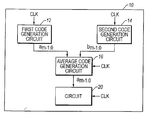
- FIG. 1 illustrates relevant components of an integrated circuit 10 in block diagram form.
- Integrated circuit 10 includes sub-circuits 12 - 20 . More particularly integrated circuit 10 includes first and second code generation sub-circuits 12 and 14 , having outputs coupled to a pair of inputs of average code generation sub-circuit 16 .
- integrated circuit 10 includes a sub-circuit 20 having an input which is coupled to the output of average code generation sub-circuit 16 .
- the term coupled circuits means that two circuits or sub-circuits that are directly or indirectly coupled together.
- first code generation sub-circuit 12 is coupled to sub-circuit 20 although coupled via average code generation sub-circuit 16 .
- Average code generation sub-circuit 16 operates upon binary codes a m ⁇ 1:0 and b m ⁇ 1:0 . More particularly, average code generation circuit generates an average binary code c m ⁇ 1:0 which represents the average of binary codes a m ⁇ 1:0 and b m ⁇ 1:0 .
- Average code generation sub-circuit 16 is a synchronous circuit and operates as a function of a clock signal (CLK) received thereby. In other words, average code generation sub-circuit 16 generates binary code c m ⁇ 1:0 upon a falling or rising edge of the clock signal CLK. It is noted that first and second code generation circuits 12 and 14 are also shown to be synchronous sub-circuits. Average binary code c m ⁇ 1:0 is provided to sub-circuit 20 which in turn performs some function in response to receiving c m ⁇ 1:0 .
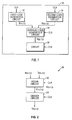
- FIG. 2 illustrates, in block diagram form, the relevant components of average code generation sub-circuit 16 of FIG. 1. More particularly, average code generation sub-circuit shown 16 in FIG. 2 includes an adder sub-circuit 22 coupled to a divider sub-circuit 24 .
- the adder and divider sub-circuits 22 and 24 are shown as synchronous circuits in that they operate as a function of the clock signal CLK provided thereto.
- Adder sub-circuit 22 receives binary codes a m ⁇ 1:0 and b m ⁇ 1:0 from first and second code generations sub-circuits 12 and 14 , respectively.
- adder sub-circuit 22 In response, adder sub-circuit 22 generates c′ m ⁇ 1:0 which represents an addition of binary codes a m ⁇ 1:0 and b m ⁇ 1:0 .
- Divider sub-circuit 24 operates to divide c′ m ⁇ 1:0 by two to generate average binary code c m ⁇ 1:0 .
- One goal in integrated circuit design is to reduce the total substrate area occupied by the integrated circuit.
- the adder and divider sub-circuits 22 and 24 may occupy a substantial area of the substrate upon which integrated circuit 10 is formed.
- Another goal in integrated circuit design is to reduce the complexity of sub-circuits.
- the adder and divider sub-circuits 22 and 24 are generally complex (i.e., they consist of a large number of interconnected gates) and require substantial design effort to implement and verify.
- Still yet another goal in integrated circuit design is to increase the speed at which the integrated circuit or sub-circuits thereof operate. Adder and divider circuits 22 and 24 are synchronous.
- a certain amount of time delay exists between generation of the average binary code c m ⁇ 1:0 from the input binary codes a m ⁇ 1:0 and b m ⁇ 1:0 . This time delay is dependent upon the frequency of the clock signal CLK provided to adder and divider sub-circuits 22 and 24 .
- the circuit may be employed in an integrated circuit having first and second circuits for generating binary codes a m ⁇ 1:0 and b m ⁇ 1:0 , respectively.
- the circuit asynchronously generates a binary code c m ⁇ 1:0 representing an average of the binary codes a m ⁇ 1:0 and b m ⁇ 1:0 generated by the first and second circuits, respectively.
- FIG. 1 is a block diagram illustrating relevant components of an integrated circuit
- FIG. 2 is a block diagram illustrating relevant components of the average code generation circuit shown in FIG. 1;
- FIG. 3 is a block diagram illustrating relevant components of an integrated circuit employing the present invention.
- FIG. 4 illustrates exemplary states of the binary codes a m ⁇ 1:0 , b m ⁇ 1:0 , and c m ⁇ 1:0 ;
- FIGS. 5 A-C are flow charts illustrating operational aspects of the average code generation circuit shown in FIG. 3;
- FIG. 6 is a block diagram illustrating relevant components of one embodiment of the average code generation circuit shown in FIG. 3;
- FIG. 7 is a block diagram illustrating relevant components of one embodiment of the sub-circuits of the average code generation circuit shown in FIG. 6.
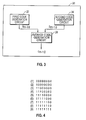
- FIG. 3 illustrates relevant components of an integrated circuit 30 implying one embodiment of the present invention.
- Integrated circuit 30 may take many forms including a microprocessor having a plurality of input and output devices that communicate with a memory device via an intervening data bus.
- FIG. 3 shows first and second code generation sub-circuits 32 and 34 coupled to an average code generation sub-circuit 36 .
- First and second code generation sub-circuits 32 and 34 respectively, generate binary codes a m ⁇ 1:0 and b m ⁇ 1:0 respectively.
- Average code generation sub-circuit 36 includes a pair of inputs for receiving respective binary codes a m ⁇ 1:0 and b m ⁇ 1:0 . It is noted that average code generation sub-circuit 36 should not be limited to a two input circuit.
- average code generation sub-circuit 36 shown in FIG. 3 is an asynchronous circuit. In other words, no clock signal is provided to average code generation sub-circuit 36 shown in FIG. 3.
- Average code generation sub-circuit 36 generates average binary code c m ⁇ 1:0 almost immediately upon receiving a m ⁇ 1:0 and b m ⁇ 1:0 .
- average code generation sub-circuit 36 shown in FIG. 3 generates average binary code c m ⁇ 1:0 in a shorter amount of time when compared to average code generation circuit shown in FIG. 1.
- first and second generation sub-circuits 32 and 34 generating 8 bit binary codes a 7:0 and b 7:0 , respectively, and with average code generation sub-circuit 36 generating an 8 bit average binary code c 7:0 in response to average code generation sub-circuit 36 receiving binary codes a 7:0 and b 7:0 .
- the present invention should not be limited thereto.
- Average code generation sub-circuit 36 generates average binary code c 7:0 . in response to receiving binary codes a 7:0 and b 7:0 .
- the average code c 7:0 generated by sub-circuit 36 may be used to control delay circuits 44(0)-44(7) of U.S. patent application Ser. No. ______, (Attorney Docket Number SP-6295 US) filed ______, entitled “Variably Controlled Delay Line for Read Data Capture Timing Window” by Cong Khieu and Louise Gu, which is incorporated herein by reference in its entirety.
- 6,060,907 may need to be remapped in accordance with the following: CNT BIT 1D ⁇ b 7 CNT BIT 2D ⁇ b 6 CNT BIT 3D ⁇ b 5 CNT BIT 4D ⁇ b 4 CNT BIT 5D ⁇ b 3 CNT BIT 6D ⁇ b 2 CNT BIT 7D ⁇ b 1 CNT BIT 8D ⁇ b 0
- the present invention will also be described with reference to sub-circuits 32 - 36 generating binary codes a 7:0 , b 7:0 , and c 7:0 that equal one of the nine binary code states (1)-(9) shown in FIG. 4, it being understood that the present invention should not be limited thereto.
- the far left bit in each of the nine binary code states represents the most significant bit while the far right bit in each of the nine code states represents the least significant bit.
- first and second code generation sub-circuits 32 and 34 will be described as synchronous circuits that generate to a 7:0 and b 7:0 , respectively, upon each rising edge of a clock signal provided thereto or upon each xth rising edge of the clock signal provided thereto.
- each generated binary code a 7:0 and b 7:0 generated by first and second code generation sub-circuits 32 and 34 respectively, differs from the previously generated binary code a 7:0 and b 7:0 , respectively, by only one bit, it being understood that the present invention should not be limited thereto.
- first code generation circuit 32 may generate a 7:0 which equals binary code state (4) shown in FIG. 4.
- the next binary code a 7:0 generated by first code generation circuit 32 may equal binary code state (3) or (5) shown in FIG. 4. Regardless of whether the next binary code a 7:0 equals binary code state (3) or (5) shown in FIG. 4, the next binary code a 7:0 differs from the previously generated binary code a 7:0 (which equals binary code state (4) of FIG. 4 ) by only one bit.
- first and second code generation sub-circuits 32 and 34 respectively, generating binary codes a 7:0 and b 7:0 which differ by five bits or fewer, it being understood that the present invention should not be limited thereto.
- first code generation circuit 32 generates binary code a 7:0 at time t 0 equal to binary code state (9) in FIG. 4
- second code generation circuit 34 generates binary code b 7:0 at time t 0 equal to one and only one of the binary code states (4)-(8) in FIG. 4.
- average code generation sub-circuit 36 generates average code c 7:0 which represents an average of a 7:0 and b 7:0 .
- An average of two distinct binary state codes may vary according to the definition of the term average.
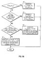
- FIGS. 5 A- 5 C are provided to illustrate various definitions of the term average as used herein.
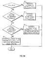
- FIG. 5A illustrates operational aspects of average code generation sub-circuit 36 operating in accordance with one embodiment of the present invention.
- FIG. 5A shows in step 40 that if a 7:0 and b 7:0 are equal to each other, then average code generation sub-circuit 36 generates c 7:0 equal to one of the inputs a 7:0 or b 7:0 . It is noted that the average code generation sub-circuit 36 does not perform the operation of comparing a 7:0 to b 7:0 .
- average code generation sub-circuit 36 If a 7:0 and b 7:0 differ from each other by only one bit, then, as shown in step 42 , average code generation sub-circuit 36 generates average code c 7:0 which equals the lesser of a 7:0 or b 7:0 .
- a 7:0 is less than b 7:0 if the total number of bits set to logical one in a 7:0 is less than the total number of bits set to logical one in b 7:0 , or vice versa.
- average code generation sub-circuit 36 does not count the total number of bits of a 7:0 or b 7:0 set to logical one, nor does average code generation sub-circuit 36 compare the total number of bits set to logical one in a 7:0 and b 7:0 .
- step 42 suppose a 7:0 and b 7:0 equal the binary state codes shown immediately below.
- code generation sub-circuit 36 In response to receiving a 7:0 and b 7:0 immediately above, code generation sub-circuit 36 , according to step 42 , generates c 7:0 equal to:
- average code generation sub-circuit 36 If a 7:0 differs from b 7:0 by only two bits, then average code generation sub-circuit 36 generates c 7:0 which equals the greater of a 7:0 or b 7:0 left shifted by one bit with logical zero fill at the least significant bit as shown in step 44 . It is noted that average code generation sub-circuit 36 does not perform a shifting operation on either input codes a 7:0 or b 7:0 . Rather, average code generation sub-circuit 36 generates c 7:0 in step 44 as if average code generation sub-circuit 36 performed the shifting operation on one of the codes a 7:0 or b 7:0 .
- step 44 suppose a 7:0 and b 7:0 equal the binary state codes shown immediately below.
- code generation sub-circuit 36 In response to receiving a 7:0 and b 7:0 immediately above, code generation sub-circuit 36 , according to step 44 , generates c 7:0 equal to:
- average code generation sub-circuit 36 If a 7:0 differs from b 7:0 by three or more bits, then average code generation sub-circuit 36 generates c 7:0 which equals the greater of a 7:0 or b 7:0 left shifted by two bits with logical zero fill at the least significant bit as shown in step 46 . Again, it is noted that the average code generation sub-circuit 36 does not perform a logical shifting operation on either of the binary code inputs.
- step 46 suppose a 7:0 and b 7:0 equal the binary state codes shown immediately below.
- code generation sub-circuit 36 In response to receiving a 7:0 and b 7:0 immediately above, code generation sub-circuit 36 , according to step 46 , generates c 7:0 equal to:
- FIG. 5B illustrates operational aspects of average code generation sub-circuit 36 operating in accordance with another embodiment of the present invention.
- FIG. 5B shows in step 40 that if a 7:0 and b 7.0 are equal to each other, then average code generation sub-circuit 36 generates c 7:0 equal to one of the inputs a 7:0 or b 7:0 .
- Average code generation sub-circuit 36 does not perform the operation of comparing a 7:0 to b 7:0 .
- average code generation sub-circuit 36 If a 7:0 and b 7:0 differ from each other by only one bit, then, as shown in step 50 , average code generation sub-circuit 36 generates average code c 7:0 which equals the greater of a 7:0 or b 7:0 . Average code generation sub-circuit 36 does not count the total number of bits of a 7:0 or b 7:0 set to logical one, nor does average code generation sub-circuit 36 compare the total number of bits set to logical one in a 7:0 and b 7:0 .
- step 50 suppose a 7:0 and b 7:0 equal the binary state codes shown immediately below.
- code generation sub-circuit 36 In response to receiving a 7:0 and b 7:0 immediately above, code generation sub-circuit 36 , according to step 50 , generates c 7:0 equal to:
- average code generation sub-circuit 36 If a 7:0 differs from b 7:0 by only two bits or only three bits, then average code generation sub-circuit 36 generates c 7:0 which equals the greater of a 7:0 or b 7:0 left shifted by one bit with logical zero fill at the least significant bit as shown in step 44 . Average code generation sub-circuit 36 does not perform a shifting operation on either input codes a 7:0 or b 7:0 .
- step 44 of FIG. 5B suppose a 7:0 and b 7:0 equal the binary state codes shown immediately below.
- code generation sub-circuit 36 In response to receiving a 7:0 and b 7:0 immediately above, code generation sub-circuit 36 , according to step 44 of FIG. 5B, generates c 7:0 equal to:
- average code generation sub-circuit 36 If a 7:0 differs from b 7:0 by more than three bits, then average code generation sub-circuit 36 generates c 7:0 which equals the greater of a 7:0 or b 7:0 left shifted by two bits with logical zero fill at the least significant bit as shown in step 46 of FIG. 5B.
- step 46 of FIG. 5B suppose a 7:0 and b 7:0 equal the binary state codes shown immediately below.
- code generation sub-circuit 36 In response to receiving a 7:0 and b 7:0 immediately above, code generation sub-circuit 36 , according to step 46 of FIG. 5B, generates c 7:0 equal to:
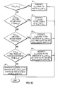
- FIG. 5C illustrates operational aspects of average code generation sub-circuit 36 operating in accordance with yet another embodiment of the present invention.
- FIG. 5C shows in step 40 that if a 7:0 and b 7:0 are equal to each other, then average code generation sub-circuit 36 generates c 7:0 equal to one of the inputs a 7:0 or b 7:0 .
- Average code generation sub-circuit 36 does not perform the operation of comparing a 7:0 to b 7:0 .
- average code generation sub-circuit 36 If a 7:0 and b 7:0 differ from each other by only one bit, then, as shown in step 42 of FIG. 5C, average code generation sub-circuit 36 generates average code c 7:0 which equals the lesser of a 7:0 or b 7:0 . Average code generation sub-circuit 36 does not count the total number of bits of a 7:0 or b 7:0 which are set to logical one, nor does average code generation sub-circuit 36 compare the total number of bits set to logical one in a 7:0 and b 7:0 .
- step 42 of FIG. 5C suppose a 7:0 and b 7:0 equal the binary state codes shown immediately below.
- code generation sub-circuit 36 In response to receiving a 7:0 and b 7:0 immediately above, code generation sub-circuit 36 , according to step 42 of FIG. 5C, generates c 7:0 equal to:
- average code generation sub-circuit 36 If a 7:0 differs from b 7:0 by only two bits, then average code generation sub-circuit 36 generates c 7:0 which equals the greater of a 7:0 or b 7:0 left shifted by one bit with logical zero fill at the least significant bit as shown in step 44 of FIG. 5C. Average code generation sub-circuit 36 does not perform a shifting operation on either input codes a 7:0 or b 7:0 .
- step 44 of FIG. 5C suppose a 7:0 and b 7:0 equal the binary state codes shown immediately below.
- code generation sub-circuit 36 In response to receiving a 7:0 and b 7:0 immediately above, code generation sub-circuit 36 , according to step 44 of FIG. 5C, generates c 7:0 equal to:
- average code generation sub-circuit 36 If a 7:0 differs from b 7:0 by only three bits or only four bits, then average code generation sub-circuit 36 generates c 7:0 which equals the greater of a 7:0 or b 7:0 left shifted by two bits with logical zero fill at the least significant bit as shown in step 46 of FIG. 5C.
- step 46 of FIG. 5C suppose a 7:0 and b 7:0 equal the binary state codes shown immediately below.
- code generation sub-circuit 36 In response to receiving a 7:0 and b 7:0 immediately above, code generation sub-circuit 36 , according to step 46 of FIG. 5C, generates c 7:0 equal to:
- average code generation sub-circuit 36 If a 7:0 differs from b 7:0 by only five bits, then average code generation sub-circuit 36 generates c 7:0 which equals the greater of a 7:0 or b 7:0 left shifted by three bits with logical zero fill at the least significant bit as shown in step 52 .
- step 52 suppose a 7:0 and b 7:0 equal the binary state codes shown immediately below.
- code generation sub-circuit 36 In response to receiving a 7:0 and b 7:0 immediately above, code generation sub-circuit 36 , according to step 52 , generates c 7:0 equal to:
- average code generation sub-circuit 36 is an asynchronous circuit.
- average code generation sub-circuit 36 consists entirely of logic gates (e.g., AND gates, NAND gates, OR gates, NOR gates, inventor gates, etc.) for generating average code c 7:0 in response to receiving input binary codes a 7:0 and b 7:0 .
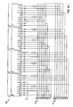
- FIG. 6 (divided into FIGS. 6A and 6B) illustrates in block diagram form one embodiment of the average code generation sub-circuit 36 shown in FIG. 4.
- Circuit 36 shown in FIG. 6 includes 8 sub-circuits 70 ( 0 ) through 70 ( 7 ).
- sub-circuit 36 shown in FIG. 6 includes a plurality of inverting gates 72 as will be fully described below.
- sub-circuits 70 ( 0 ) through 70 ( 7 ) are identical to each other.
- each of the circuits 70 ( 0 )- 70 ( 7 ) includes ten inputs and a single output c n .
- the inputs of circuits 70 ( 0 )- 70 ( 7 ) are designated as shown in FIG. 6.
- the inputs are coupled to receive bits of input binary codes a 7:0 and b 7:0 as shown.
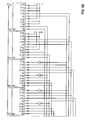
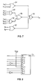
- FIG. 7 illustrates one embodiment of circuits 70 ( 0 )- 70 ( 7 ) shown in FIG. 6. More particularly, FIG.
- sub-circuits 70 ( 0 )- 70 ( 7 ) may take form in a combination of logic gates different than what is shown in FIG. 7.
Abstract
Description
- Integrated circuits including microprocessors often contain sub-circuits that generate multibit binary codes for controlling other sub-circuits within the integrated circuit. Often times, these integrated circuits require the averaging of two or more of the multibit binary codes, the result of which is used to control another sub-circuit. Typically, an adder sub-circuit and a divider sub-circuit operating together perform the function of averaging binary codes.
- FIG. 1 illustrates relevant components of an
integrated circuit 10 in block diagram form.Integrated circuit 10 includes sub-circuits 12-20. More particularly integratedcircuit 10 includes first and secondcode generation sub-circuits code generation sub-circuit 16. Lastly integratedcircuit 10 includes asub-circuit 20 having an input which is coupled to the output of averagecode generation sub-circuit 16. For purposes of explanation, the term coupled circuits means that two circuits or sub-circuits that are directly or indirectly coupled together. For example, firstcode generation sub-circuit 12 is coupled tosub-circuit 20 although coupled via averagecode generation sub-circuit 16. - Average
code generation sub-circuit 16 operates upon binary codes am−1:0 and bm−1:0. More particularly, average code generation circuit generates an average binary code cm−1:0 which represents the average of binary codes am−1:0 and bm−1:0. Averagecode generation sub-circuit 16 is a synchronous circuit and operates as a function of a clock signal (CLK) received thereby. In other words, averagecode generation sub-circuit 16 generates binary code cm−1:0 upon a falling or rising edge of the clock signal CLK. It is noted that first and secondcode generation circuits - FIG. 2 illustrates, in block diagram form, the relevant components of average
code generation sub-circuit 16 of FIG. 1. More particularly, average code generation sub-circuit shown 16 in FIG. 2 includes anadder sub-circuit 22 coupled to adivider sub-circuit 24. The adder anddivider sub-circuits Adder sub-circuit 22 receives binary codes am−1:0 and bm−1:0 from first and secondcode generations sub-circuits adder sub-circuit 22 generates c′m−1:0 which represents an addition of binary codes am−1:0 and bm−1:0.Divider sub-circuit 24 operates to divide c′m−1:0 by two to generate average binary code cm−1:0. - One goal in integrated circuit design is to reduce the total substrate area occupied by the integrated circuit. Unfortunately, the adder and
divider sub-circuits integrated circuit 10 is formed. Another goal in integrated circuit design is to reduce the complexity of sub-circuits. The adder anddivider sub-circuits divider circuits sub-circuits - Disclosed is a method and circuit for generating an average binary code from at least two input binary codes. The circuit may be employed in an integrated circuit having first and second circuits for generating binary codes a m−1:0 and bm−1:0, respectively. In one embodiment, the circuit asynchronously generates a binary code cm−1:0 representing an average of the binary codes am−1:0 and bm−1:0 generated by the first and second circuits, respectively.
- The present invention may be better understood, and its numerous objects, features and advantages made apparent to those skilled in the art by referencing the accompanying drawings. The use of the same reference number throughout the Figures designates a like or similar element.
- FIG. 1 is a block diagram illustrating relevant components of an integrated circuit;
- FIG. 2 is a block diagram illustrating relevant components of the average code generation circuit shown in FIG. 1;
- FIG. 3 is a block diagram illustrating relevant components of an integrated circuit employing the present invention;
- FIG. 4 illustrates exemplary states of the binary codes a m−1:0, bm−1:0, and cm−1:0;
- FIGS. 5A-C are flow charts illustrating operational aspects of the average code generation circuit shown in FIG. 3;
- FIG. 6 is a block diagram illustrating relevant components of one embodiment of the average code generation circuit shown in FIG. 3;
- FIG. 7 is a block diagram illustrating relevant components of one embodiment of the sub-circuits of the average code generation circuit shown in FIG. 6.
- While the invention is susceptible to various modifications and alternative forms, specific embodiments thereof are shown by way of example in the drawings and will herein be described in detail. However, the drawings and detailed description thereto are not intended to limit the invention to the particular form disclosed. On the contrary, the intention is to cover all modifications, equivalents, and alternatives falling within the spirit and scope of the present invention as defined by the appended claims.
- FIG. 3 illustrates relevant components of an integrated
circuit 30 implying one embodiment of the present invention.Integrated circuit 30 may take many forms including a microprocessor having a plurality of input and output devices that communicate with a memory device via an intervening data bus. FIG. 3 shows first and secondcode generation sub-circuits code generation sub-circuit 36. First and secondcode generation sub-circuits code generation sub-circuit 36 includes a pair of inputs for receiving respective binary codes am−1:0 and bm−1:0. It is noted that averagecode generation sub-circuit 36 should not be limited to a two input circuit. - It is noted that unlike the average
code generation sub-circuit 16 shown in FIG. 1, averagecode generation sub-circuit 36 shown in FIG. 3 is an asynchronous circuit. In other words, no clock signal is provided to averagecode generation sub-circuit 36 shown in FIG. 3. Averagecode generation sub-circuit 36 generates average binary code cm−1:0 almost immediately upon receiving am−1:0 and bm−1:0. Thus, averagecode generation sub-circuit 36 shown in FIG. 3 generates average binary code cm−1:0 in a shorter amount of time when compared to average code generation circuit shown in FIG. 1. - The present invention will be described with reference to first and
second generation sub-circuits code generation sub-circuit 36 generating an 8 bit average binary code c7:0 in response to averagecode generation sub-circuit 36 receiving binary codes a7:0 and b7:0. The present invention should not be limited thereto. - Average
code generation sub-circuit 36 generates average binary code c7:0. in response to receiving binary codes a7:0 and b7:0. Although not shown in the figures, the average code c7:0 generated bysub-circuit 36 may be used to control delay circuits 44(0)-44(7) of U.S. patent application Ser. No. ______, (Attorney Docket Number SP-6295 US) filed ______, entitled “Variably Controlled Delay Line for Read Data Capture Timing Window” by Cong Khieu and Louise Gu, which is incorporated herein by reference in its entirety. The averagecode generation sub-circuit 36 of FIG. 3 may be employed to generate an average of pull-up and pull-down control codes generated by pull-up and pull-down control circuits, respectively, described in U.S. Pat. No. 6,060,907 which is incorporated herein by reference in its entirety. It is noted, however, that the pull down control code CNT BIT 1D-CNT BIT 8D generated by the pull down control circuit described in U.S. Pat. No. 6,060,907, may need to be remapped in accordance with the following:CNT BIT 1D → b7 CNT BIT 2D → b6 CNT BIT 3D → b5 CNT BIT 4D → b4 CNT BIT 5D → b3 CNT BIT 6D → b2 CNT BIT 7D → b1 CNT BIT 8D → b0 - The present invention will also be described with reference to sub-circuits 32-36 generating binary codes a7:0, b7:0, and c7:0 that equal one of the nine binary code states (1)-(9) shown in FIG. 4, it being understood that the present invention should not be limited thereto. In FIG. 4, the far left bit in each of the nine binary code states represents the most significant bit while the far right bit in each of the nine code states represents the least significant bit.
- For purposes of explanation, first and second
code generation sub-circuits code generation sub-circuits code generation circuit 32 may generate a7:0 which equals binary code state (4) shown in FIG. 4. The next binary code a7:0 generated by firstcode generation circuit 32 may equal binary code state (3) or (5) shown in FIG. 4. Regardless of whether the next binary code a7:0 equals binary code state (3) or (5) shown in FIG. 4, the next binary code a7:0 differs from the previously generated binary code a7:0 (which equals binary code state (4) of FIG. 4) by only one bit. Lastly, the present invention will be described with reference to first and secondcode generation sub-circuits code generation circuit 32 generates binary code a7:0 at time t0 equal to binary code state (9) in FIG. 4, then secondcode generation circuit 34 generates binary code b7:0 at time t0 equal to one and only one of the binary code states (4)-(8) in FIG. 4. - As noted above, average
code generation sub-circuit 36 generates average code c7:0 which represents an average of a7:0 and b7:0. An average of two distinct binary state codes may vary according to the definition of the term average. FIGS. 5A-5C are provided to illustrate various definitions of the term average as used herein. - FIG. 5A illustrates operational aspects of average
code generation sub-circuit 36 operating in accordance with one embodiment of the present invention. FIG. 5A shows instep 40 that if a7:0 and b7:0 are equal to each other, then averagecode generation sub-circuit 36 generates c7:0 equal to one of the inputs a7:0 or b7:0. It is noted that the averagecode generation sub-circuit 36 does not perform the operation of comparing a7:0 to b7:0. - If a 7:0 and b7:0 differ from each other by only one bit, then, as shown in
step 42, averagecode generation sub-circuit 36 generates average code c7:0 which equals the lesser of a7:0 or b7:0. For purposes of definition a7:0 is less than b7:0 if the total number of bits set to logical one in a7:0 is less than the total number of bits set to logical one in b7:0, or vice versa. It is noted that averagecode generation sub-circuit 36 does not count the total number of bits of a7:0 or b7:0 set to logical one, nor does averagecode generation sub-circuit 36 compare the total number of bits set to logical one in a7:0 and b7:0. - As an example of
step 42, suppose a7:0 and b7:0 equal the binary state codes shown immediately below. - a 7:0=11000000
- b 7:0=11100000
- In response to receiving a 7:0 and b7:0 immediately above,
code generation sub-circuit 36, according to step 42, generates c7:0 equal to: - c 7:0=11000000.
- If a 7:0 differs from b7:0 by only two bits, then average
code generation sub-circuit 36 generates c7:0 which equals the greater of a7:0 or b7:0 left shifted by one bit with logical zero fill at the least significant bit as shown instep 44. It is noted that averagecode generation sub-circuit 36 does not perform a shifting operation on either input codes a7:0 or b7:0. Rather, averagecode generation sub-circuit 36 generates c7:0 instep 44 as if averagecode generation sub-circuit 36 performed the shifting operation on one of the codes a7:0 or b7:0. - As an example of
step 44, suppose a7:0 and b7:0 equal the binary state codes shown immediately below. - a 7:0=11000000
- b 7:0=11110000
- In response to receiving a 7:0 and b7:0 immediately above,
code generation sub-circuit 36, according to step 44, generates c7:0 equal to: - c 7:0=11100000,
- which is equal to b 7:0 immediately above, left shifted by one bit with logical zero fill at the least significant bit thereof.
- If a 7:0 differs from b7:0 by three or more bits, then average
code generation sub-circuit 36 generates c7:0 which equals the greater of a7:0 or b7:0 left shifted by two bits with logical zero fill at the least significant bit as shown instep 46. Again, it is noted that the averagecode generation sub-circuit 36 does not perform a logical shifting operation on either of the binary code inputs. - As an example of
step 46, suppose a7:0 and b7:0 equal the binary state codes shown immediately below. - a 7:0=11000000
- b 7:0=11111110
- In response to receiving a 7:0 and b7:0 immediately above,
code generation sub-circuit 36, according to step 46, generates c7:0 equal to: - c 7:0=11111000,
- which is equal to b 7:0 immediately above, left shifted by two bits with logical zero fill at the least significant bit thereof.
- FIG. 5B illustrates operational aspects of average
code generation sub-circuit 36 operating in accordance with another embodiment of the present invention. FIG. 5B shows instep 40 that if a7:0 and b7.0 are equal to each other, then averagecode generation sub-circuit 36 generates c7:0 equal to one of the inputs a7:0 or b7:0. Averagecode generation sub-circuit 36 does not perform the operation of comparing a7:0 to b7:0. - If a 7:0 and b7:0 differ from each other by only one bit, then, as shown in
step 50, averagecode generation sub-circuit 36 generates average code c7:0 which equals the greater of a7:0 or b7:0. Averagecode generation sub-circuit 36 does not count the total number of bits of a7:0 or b7:0 set to logical one, nor does averagecode generation sub-circuit 36 compare the total number of bits set to logical one in a7:0 and b7:0. - As an example of
step 50, suppose a7:0 and b7:0 equal the binary state codes shown immediately below. - a 7:0=11000000
- b 7:0=11100000
- In response to receiving a 7:0 and b7:0 immediately above,
code generation sub-circuit 36, according to step 50, generates c7:0 equal to: - c 7:0=11100000
- If a 7:0 differs from b7:0 by only two bits or only three bits, then average
code generation sub-circuit 36 generates c7:0 which equals the greater of a7:0 or b7:0 left shifted by one bit with logical zero fill at the least significant bit as shown instep 44. Averagecode generation sub-circuit 36 does not perform a shifting operation on either input codes a7:0 or b7:0. - As an example of
step 44 of FIG. 5B, suppose a7:0 and b7:0 equal the binary state codes shown immediately below. - a 7:0=11000000
- b 7:0=11111000
- In response to receiving a 7:0 and b7:0 immediately above,
code generation sub-circuit 36, according to step 44 of FIG. 5B, generates c7:0 equal to: - c 7:0=11110000,
- which is equal to b 7:0 immediately above, left shifted by one bit with logical zero fill at the least significant bit thereof.
- If a 7:0 differs from b7:0 by more than three bits, then average
code generation sub-circuit 36 generates c7:0 which equals the greater of a7:0 or b7:0 left shifted by two bits with logical zero fill at the least significant bit as shown instep 46 of FIG. 5B. - As an example of
step 46 of FIG. 5B, suppose a7:0 and b7:0 equal the binary state codes shown immediately below. - a 7:0=11000000
- b 7:0=11111110
- In response to receiving a 7:0 and b7:0 immediately above,
code generation sub-circuit 36, according to step 46 of FIG. 5B, generates c7:0 equal to: - c 7:0=11111000,
- which is equal to b 7:0 immediately above, left shifted by two bits with logical zero fill at the least significant bit thereof.
- FIG. 5C illustrates operational aspects of average
code generation sub-circuit 36 operating in accordance with yet another embodiment of the present invention. FIG. 5C shows instep 40 that if a7:0 and b7:0 are equal to each other, then averagecode generation sub-circuit 36 generates c7:0 equal to one of the inputs a7:0 or b7:0. Averagecode generation sub-circuit 36 does not perform the operation of comparing a7:0 to b7:0. - If a 7:0 and b7:0 differ from each other by only one bit, then, as shown in
step 42 of FIG. 5C, averagecode generation sub-circuit 36 generates average code c7:0 which equals the lesser of a7:0 or b7:0. Averagecode generation sub-circuit 36 does not count the total number of bits of a7:0 or b7:0 which are set to logical one, nor does averagecode generation sub-circuit 36 compare the total number of bits set to logical one in a7:0 and b7:0. - As an example of
step 42 of FIG. 5C, suppose a7:0 and b7:0 equal the binary state codes shown immediately below. - a 7:0=11000000
- b 7:0=11100000
- In response to receiving a 7:0 and b7:0 immediately above,
code generation sub-circuit 36, according to step 42 of FIG. 5C, generates c7:0 equal to: - c 7:0=11000000
- If a 7:0 differs from b7:0 by only two bits, then average
code generation sub-circuit 36 generates c7:0 which equals the greater of a7:0 or b7:0 left shifted by one bit with logical zero fill at the least significant bit as shown instep 44 of FIG. 5C. Averagecode generation sub-circuit 36 does not perform a shifting operation on either input codes a7:0 or b7:0. - As an example of
step 44 of FIG. 5C, suppose a7:0 and b7:0 equal the binary state codes shown immediately below. - a 7:0=11000000
- b 7:0=11110000
- In response to receiving a 7:0 and b7:0 immediately above,
code generation sub-circuit 36, according to step 44 of FIG. 5C, generates c7:0 equal to: - c 7:0=11100000,
- which is equal to b 7:0 immediately above, left shifted by one bit with logical zero fill at the least significant bit thereof.
- If a 7:0 differs from b7:0 by only three bits or only four bits, then average
code generation sub-circuit 36 generates c7:0 which equals the greater of a7:0 or b7:0 left shifted by two bits with logical zero fill at the least significant bit as shown instep 46 of FIG. 5C. - As an example of
step 46 of FIG. 5C, suppose a7:0 and b7:0 equal the binary state codes shown immediately below. - a 7:0=11000000
- b 7:0=11111100
- In response to receiving a 7:0 and b7:0 immediately above,
code generation sub-circuit 36, according to step 46 of FIG. 5C, generates c7:0 equal to: - c 7:0=11110000,
- which is equal to b 7:0 immediately above, left shifted by two bits with logical zero fill at the least significant bit thereof.
- If a 7:0 differs from b7:0 by only five bits, then average
code generation sub-circuit 36 generates c7:0 which equals the greater of a7:0 or b7:0 left shifted by three bits with logical zero fill at the least significant bit as shown instep 52. - As an example of
step 52, suppose a7:0 and b7:0 equal the binary state codes shown immediately below. - a 7:0=11000000
- b 7:0=11111110
- In response to receiving a 7:0 and b7:0 immediately above,
code generation sub-circuit 36, according to step 52, generates c7:0 equal to: - c 7:0=11110000,
- which is equal to b 7:0 immediately above, left shifted by three bits with logical zero fill at the least significant bit thereof.
- As noted above, average
code generation sub-circuit 36 is an asynchronous circuit. In one embodiment, averagecode generation sub-circuit 36 consists entirely of logic gates (e.g., AND gates, NAND gates, OR gates, NOR gates, inventor gates, etc.) for generating average code c7:0 in response to receiving input binary codes a7:0 and b7:0. FIG. 6 (divided into FIGS. 6A and 6B) illustrates in block diagram form one embodiment of the averagecode generation sub-circuit 36 shown in FIG. 4.Circuit 36 shown in FIG. 6 includes 8 sub-circuits 70(0) through 70(7). Additionally, sub-circuit 36 shown in FIG. 6 includes a plurality of inverting gates 72 as will be fully described below. - In one embodiment, sub-circuits 70(0) through 70(7) are identical to each other. In this embodiment, each of the circuits 70(0)-70(7) includes ten inputs and a single output cn. The inputs of circuits 70(0)-70(7) are designated as shown in FIG. 6. Moreover, the inputs are coupled to receive bits of input binary codes a7:0 and b7:0 as shown. FIG. 7 illustrates one embodiment of circuits 70(0)-70(7) shown in FIG. 6. More particularly, FIG. 7 shows a pair of
NAND gates gates gates gates - Although the present invention has been described in connection with several embodiments, the invention is not intended to be limited to the specific forms set forth herein. On the contrary, it is intended to cover such alternatives, modifications, and equivalents as can be reasonably included within the spirit and scope of the invention as defined by the appended claims.
Claims (11)
Priority Applications (1)
| Application Number | Priority Date | Filing Date | Title |
|---|---|---|---|
| US10/158,695 US7254599B2 (en) | 2002-05-30 | 2002-05-30 | Average code generation circuit |
Applications Claiming Priority (1)
| Application Number | Priority Date | Filing Date | Title |
|---|---|---|---|
| US10/158,695 US7254599B2 (en) | 2002-05-30 | 2002-05-30 | Average code generation circuit |
Publications (2)
| Publication Number | Publication Date |
|---|---|
| US20030225804A1 true US20030225804A1 (en) | 2003-12-04 |
| US7254599B2 US7254599B2 (en) | 2007-08-07 |
Family
ID=29582737
Family Applications (1)
| Application Number | Title | Priority Date | Filing Date |
|---|---|---|---|
| US10/158,695 Active 2024-08-06 US7254599B2 (en) | 2002-05-30 | 2002-05-30 | Average code generation circuit |
Country Status (1)
| Country | Link |
|---|---|
| US (1) | US7254599B2 (en) |
Families Citing this family (1)
| Publication number | Priority date | Publication date | Assignee | Title |
|---|---|---|---|---|
| TWI260134B (en) * | 2005-04-22 | 2006-08-11 | Sunplus Technology Co Ltd | Apparatus and method of energy detection |
Citations (22)
| Publication number | Priority date | Publication date | Assignee | Title |
|---|---|---|---|---|
| US4368433A (en) * | 1979-08-25 | 1983-01-11 | Fujitsu Fanuc Limited | Signal converter circuit |
| US4789953A (en) * | 1985-03-19 | 1988-12-06 | Battelle-Institut E.V. | Circuit arrangement for averaging |
| US5751617A (en) * | 1996-04-22 | 1998-05-12 | Samsung Electronics Co., Ltd. | Calculating the average of two integer numbers rounded away from zero in a single instruction cycle |
| US5883824A (en) * | 1993-11-29 | 1999-03-16 | Hewlett-Packard Company | Parallel adding and averaging circuit and method |
| US5955894A (en) * | 1997-06-25 | 1999-09-21 | Sun Microsystems, Inc. | Method for controlling the impedance of a driver circuit |
| US5999978A (en) * | 1997-10-31 | 1999-12-07 | Sun Microsystems, Inc. | Distributed system and method for controlling access to network resources and event notifications |
| US6007232A (en) * | 1996-11-14 | 1999-12-28 | Samsung Electronics Co., Ltd. | Calculating the average of two integer numbers rounded towards zero in a single instruction cycle |
| US6060907A (en) * | 1997-06-25 | 2000-05-09 | Sun Microsystems, Inc. | Impedance control circuit |
| US6064656A (en) * | 1997-10-31 | 2000-05-16 | Sun Microsystems, Inc. | Distributed system and method for controlling access control to network resources |
| US6085033A (en) * | 1997-06-25 | 2000-07-04 | Sun Microsystems, Inc. | Method for determining bit element values for driver impedance control |
| US6212511B1 (en) * | 1997-10-31 | 2001-04-03 | Sun Microsystems, Inc. | Distributed system and method for providing SQL access to management information in a secure distributed network |
| US6226664B1 (en) * | 1992-09-30 | 2001-05-01 | Texas Instruments Incorporated | Method and device for adding and subtracting thermometer coded data |
| US6278306B1 (en) * | 1999-06-07 | 2001-08-21 | Sun Microsystems, Inc. | Method for an output driver with improved slew rate control |
| US6281729B1 (en) * | 1999-06-07 | 2001-08-28 | Sun Microsystems, Inc. | Output driver with improved slew rate control |
| US6294924B1 (en) * | 1999-09-20 | 2001-09-25 | Sun Microsystems, Inc. | Dynamic termination logic driver with improved slew rate control |
| US6297677B1 (en) * | 1999-09-20 | 2001-10-02 | Sun Microsystems, Inc. | Method for a dynamic termination logic driver with improved slew rate control |
| US6316957B1 (en) * | 1999-09-20 | 2001-11-13 | Sun Microsystems, Inc. | Method for a dynamic termination logic driver with improved impedance control |
| US6339351B1 (en) * | 1999-06-07 | 2002-01-15 | Sun Microsystems, Inc. | Output driver with improved impedance control |
| US6366139B1 (en) * | 1999-06-07 | 2002-04-02 | Sun Microsystems, Inc. | Method for an output driver with improved impedance control |
| US6420913B1 (en) * | 1999-09-20 | 2002-07-16 | Sun Microsystems, Inc. | Dynamic termination logic driver with improved impedance control |
| US20030097389A1 (en) * | 2001-11-21 | 2003-05-22 | Ashley Saulsbury | Methods and apparatus for performing pixel average operations |
| US6795841B2 (en) * | 2000-05-23 | 2004-09-21 | Arm Limited | Parallel processing of multiple data values within a data word |
-
2002
- 2002-05-30 US US10/158,695 patent/US7254599B2/en active Active
Patent Citations (22)
| Publication number | Priority date | Publication date | Assignee | Title |
|---|---|---|---|---|
| US4368433A (en) * | 1979-08-25 | 1983-01-11 | Fujitsu Fanuc Limited | Signal converter circuit |
| US4789953A (en) * | 1985-03-19 | 1988-12-06 | Battelle-Institut E.V. | Circuit arrangement for averaging |
| US6226664B1 (en) * | 1992-09-30 | 2001-05-01 | Texas Instruments Incorporated | Method and device for adding and subtracting thermometer coded data |
| US5883824A (en) * | 1993-11-29 | 1999-03-16 | Hewlett-Packard Company | Parallel adding and averaging circuit and method |
| US5751617A (en) * | 1996-04-22 | 1998-05-12 | Samsung Electronics Co., Ltd. | Calculating the average of two integer numbers rounded away from zero in a single instruction cycle |
| US6007232A (en) * | 1996-11-14 | 1999-12-28 | Samsung Electronics Co., Ltd. | Calculating the average of two integer numbers rounded towards zero in a single instruction cycle |
| US6085033A (en) * | 1997-06-25 | 2000-07-04 | Sun Microsystems, Inc. | Method for determining bit element values for driver impedance control |
| US5955894A (en) * | 1997-06-25 | 1999-09-21 | Sun Microsystems, Inc. | Method for controlling the impedance of a driver circuit |
| US6060907A (en) * | 1997-06-25 | 2000-05-09 | Sun Microsystems, Inc. | Impedance control circuit |
| US6212511B1 (en) * | 1997-10-31 | 2001-04-03 | Sun Microsystems, Inc. | Distributed system and method for providing SQL access to management information in a secure distributed network |
| US6064656A (en) * | 1997-10-31 | 2000-05-16 | Sun Microsystems, Inc. | Distributed system and method for controlling access control to network resources |
| US5999978A (en) * | 1997-10-31 | 1999-12-07 | Sun Microsystems, Inc. | Distributed system and method for controlling access to network resources and event notifications |
| US6278306B1 (en) * | 1999-06-07 | 2001-08-21 | Sun Microsystems, Inc. | Method for an output driver with improved slew rate control |
| US6281729B1 (en) * | 1999-06-07 | 2001-08-28 | Sun Microsystems, Inc. | Output driver with improved slew rate control |
| US6339351B1 (en) * | 1999-06-07 | 2002-01-15 | Sun Microsystems, Inc. | Output driver with improved impedance control |
| US6366139B1 (en) * | 1999-06-07 | 2002-04-02 | Sun Microsystems, Inc. | Method for an output driver with improved impedance control |
| US6294924B1 (en) * | 1999-09-20 | 2001-09-25 | Sun Microsystems, Inc. | Dynamic termination logic driver with improved slew rate control |
| US6297677B1 (en) * | 1999-09-20 | 2001-10-02 | Sun Microsystems, Inc. | Method for a dynamic termination logic driver with improved slew rate control |
| US6316957B1 (en) * | 1999-09-20 | 2001-11-13 | Sun Microsystems, Inc. | Method for a dynamic termination logic driver with improved impedance control |
| US6420913B1 (en) * | 1999-09-20 | 2002-07-16 | Sun Microsystems, Inc. | Dynamic termination logic driver with improved impedance control |
| US6795841B2 (en) * | 2000-05-23 | 2004-09-21 | Arm Limited | Parallel processing of multiple data values within a data word |
| US20030097389A1 (en) * | 2001-11-21 | 2003-05-22 | Ashley Saulsbury | Methods and apparatus for performing pixel average operations |
Also Published As
| Publication number | Publication date |
|---|---|
| US7254599B2 (en) | 2007-08-07 |
Similar Documents
| Publication | Publication Date | Title |
|---|---|---|
| Lin et al. | A novel high-speed and energy efficient 10-transistor full adder design | |
| US6498515B2 (en) | Semiconductor integrated circuit and method for designing the same | |
| US6185719B1 (en) | Pass-transistor logic circuit and a method of designing thereof | |
| EP0606912B1 (en) | CMOS polyphase clock generation circuits | |
| US5511222A (en) | Priority encoder | |
| US7015600B2 (en) | Pulse generator circuit and semiconductor device including same | |
| US5724287A (en) | Data input circuit of semiconductor storage device | |
| US5977809A (en) | Programmable non-overlap clock generator | |
| KR100429892B1 (en) | High speed binary comparator circuit and High speed binary data comparison method | |
| US5329477A (en) | Adder circuit having carry signal initializing circuit | |
| US7783690B2 (en) | Electronic circuit for implementing a permutation operation | |
| US7254599B2 (en) | Average code generation circuit | |
| US6938223B2 (en) | Logic circuit having a functionally redundant transistor network | |
| US6928572B2 (en) | Multistage clock delay circuit and method | |
| US6504407B2 (en) | Programmable high speed frequency divider | |
| US6003059A (en) | Carry select adder using two level selectors | |
| EP0311102B1 (en) | Semiconductor ic including circuit for preventing erroneous operation caused by power source noise | |
| US6185720B1 (en) | Slaveless synchronous system design | |
| US6738792B1 (en) | Parallel mask generator | |
| US5946369A (en) | High-speed binary synchronous counter with precomputation of carry-independent terms | |
| US6396896B1 (en) | Implementation of functions of multiple successive bits of a shift register | |
| US5493525A (en) | Carry-chain compiler | |
| US6701423B2 (en) | High speed address sequencer | |
| US7085796B1 (en) | Dynamic adder with reduced logic | |
| US7042246B2 (en) | Logic circuits for performing threshold functions |
Legal Events
| Date | Code | Title | Description |
|---|---|---|---|
| AS | Assignment |
Owner name: SUN MICROSYSTEMS, INC., CALIFORNIA Free format text: ASSIGNMENT OF ASSIGNORS INTEREST;ASSIGNORS:KHIEU, CONG Q.;GU, LOUISE;REEL/FRAME:013174/0010;SIGNING DATES FROM 20020513 TO 20020715 |
|
| STCF | Information on status: patent grant |
Free format text: PATENTED CASE |
|
| CC | Certificate of correction | ||
| FPAY | Fee payment |
Year of fee payment: 4 |
|
| FPAY | Fee payment |
Year of fee payment: 8 |
|
| AS | Assignment |
Owner name: ORACLE AMERICA, INC., CALIFORNIA Free format text: MERGER AND CHANGE OF NAME;ASSIGNORS:ORACLE USA, INC.;SUN MICROSYSTEMS, INC.;ORACLE AMERICA, INC.;REEL/FRAME:037302/0843 Effective date: 20100212 |
|
| MAFP | Maintenance fee payment |
Free format text: PAYMENT OF MAINTENANCE FEE, 12TH YEAR, LARGE ENTITY (ORIGINAL EVENT CODE: M1553); ENTITY STATUS OF PATENT OWNER: LARGE ENTITY Year of fee payment: 12 |