US20030227983A1 - Active polyphase inverter filter for quadrature signal generation - Google Patents
Active polyphase inverter filter for quadrature signal generation Download PDFInfo
- Publication number
- US20030227983A1 US20030227983A1 US10/453,622 US45362203A US2003227983A1 US 20030227983 A1 US20030227983 A1 US 20030227983A1 US 45362203 A US45362203 A US 45362203A US 2003227983 A1 US2003227983 A1 US 2003227983A1
- Authority
- US
- United States
- Prior art keywords
- delay circuit
- output
- quadrature
- degree
- signals
- Prior art date
- Legal status (The legal status is an assumption and is not a legal conclusion. Google has not performed a legal analysis and makes no representation as to the accuracy of the status listed.)
- Granted
Links
- 230000007274 generation of a signal involved in cell-cell signaling Effects 0.000 title claims description 8
- 238000000034 method Methods 0.000 claims abstract description 21
- 230000003111 delayed effect Effects 0.000 claims description 20
- 238000012935 Averaging Methods 0.000 claims description 15
- 238000007670 refining Methods 0.000 claims 6
- 230000008569 process Effects 0.000 abstract description 10
- 230000003071 parasitic effect Effects 0.000 description 13
- 230000005540 biological transmission Effects 0.000 description 9
- 239000003990 capacitor Substances 0.000 description 9
- 238000005070 sampling Methods 0.000 description 8
- 230000000630 rising effect Effects 0.000 description 7
- 230000010355 oscillation Effects 0.000 description 6
- 230000010363 phase shift Effects 0.000 description 6
- 239000004065 semiconductor Substances 0.000 description 6
- 238000001228 spectrum Methods 0.000 description 6
- 230000008901 benefit Effects 0.000 description 5
- 230000001934 delay Effects 0.000 description 5
- 230000000737 periodic effect Effects 0.000 description 5
- 239000000758 substrate Substances 0.000 description 4
- 230000000694 effects Effects 0.000 description 3
- 238000003780 insertion Methods 0.000 description 3
- 230000037431 insertion Effects 0.000 description 3
- 230000001419 dependent effect Effects 0.000 description 2
- 238000002474 experimental method Methods 0.000 description 2
- 230000014509 gene expression Effects 0.000 description 2
- 230000006872 improvement Effects 0.000 description 2
- 238000012546 transfer Methods 0.000 description 2
- 230000000903 blocking effect Effects 0.000 description 1
- 239000000969 carrier Substances 0.000 description 1
- 238000012937 correction Methods 0.000 description 1
- 238000000354 decomposition reaction Methods 0.000 description 1
- 230000007423 decrease Effects 0.000 description 1
- 230000003467 diminishing effect Effects 0.000 description 1
- 230000005669 field effect Effects 0.000 description 1
- 238000013178 mathematical model Methods 0.000 description 1
- 238000012545 processing Methods 0.000 description 1
- 230000004044 response Effects 0.000 description 1
- 230000035945 sensitivity Effects 0.000 description 1
- 230000008054 signal transmission Effects 0.000 description 1
- 230000003595 spectral effect Effects 0.000 description 1
- 230000001052 transient effect Effects 0.000 description 1
- 230000007704 transition Effects 0.000 description 1
Images


Classifications
-
- H—ELECTRICITY
- H04—ELECTRIC COMMUNICATION TECHNIQUE
- H04L—TRANSMISSION OF DIGITAL INFORMATION, e.g. TELEGRAPHIC COMMUNICATION
- H04L27/00—Modulated-carrier systems
- H04L27/32—Carrier systems characterised by combinations of two or more of the types covered by groups H04L27/02, H04L27/10, H04L27/18 or H04L27/26
- H04L27/34—Amplitude- and phase-modulated carrier systems, e.g. quadrature-amplitude modulated carrier systems
- H04L27/36—Modulator circuits; Transmitter circuits
- H04L27/362—Modulation using more than one carrier, e.g. with quadrature carriers, separately amplitude modulated
- H04L27/364—Arrangements for overcoming imperfections in the modulator, e.g. quadrature error or unbalanced I and Q levels
Definitions
- the present invention generally relates to signal generation, and more specifically to quadrature signal generation using an active polyphase inverter filter.
- I in-phase signal
- Q quadrature signal
- the Q signal is 90 degrees out of phase with the I signal. More specifically, the Q signal is delayed (or advanced) relative to the I signal (in-time) by 90 degrees.
- Quadrature amplitude modulation QAM
- quadrature phase shift keying QPSK
- the advantage of the quadrature signal transmission is that the bandwidth of a transmission medium is effectively doubled.
- quadrature modulation permits 2B (Hz) of information to be effectively transmitted through the medium without signal interference.
- the I and Q information can be discerned from each other by sampling the I and Q signals at the proper time based on the known 90 degree phase delay. However, the I and Q sampling times must be properly timed. Any error in sampling time will cause signal distortion and/or interference between the I and Q channels.
- the present invention is related to a quadrature signal generator that receives a differential input signal and generates quadrature output signals that are 90 degrees out-of-phase with each other.
- the quadrature signal generator is an open-loop architecture that utilizes active inverters for delay elements.
- the invention is also related to subcomponents and methods related to the same.
- the quadrature signal generator includes a coarse stage and a plurality of refinement stages.
- the coarse stage receives a differential input signal and generates a plurality of quadrature signals that are substantially phase-shifted by 90 degrees with respect to each other, but which may have some phase errors.
- the refinement stages receive quadrature signals from the output of the coarse stage, and process the quadrature signals to reduce the phase error between the quadrature signals. Any number of refinement stages can be utilized. The greater the number of refinement stages, the more the phase error is reduced, but subject to a point of diminishing returns.
- Each coarse stage includes a pair of 90/180 delay circuits that delay the differential signal, and generate quadrature output signals that may have some phase error.
- Each refinement stage includes a plurality of 0/180 delay circuits that each receive a corresponding quadrature output signal from the coarse stage generator, and have a 0-degree output and a 180-degree output.
- the 0-degree output of a first 0/180 delay circuit is averaged with a 180 degree output of a second 0/180 delay circuit.
- a 0-degree output of a third 0/180 delay circuit is averaged with a 180 degree output of a fourth 0/180 delay circuit.
- the averaging of the delay circuit outputs has the effect of reducing the phase error.
- the refinement stage also includes a plurality of 90/180 delay circuits having inputs coupled to corresponding 0-degree outputs of the 0/180 delay circuits.
- the 90-degree output of a first 90/180 delay circuit is averaged with a 180 degree output of a second 90/180 delay circuit.
- the 90-degree output of a third 90/180 delay circuit is coupled to a 180 degree output of a fourth 90/180 delay circuit.
- Each delay circuit 0/180 includes a first series of inverters and a second series of inverters, where the second series of inverters has an approximate total delay of 180 degrees relative to said first series of inverters.
- Each delay circuit 90/180 includes a third series of inverters and a fourth series of inverters, where the fourth series of inverters has a delay of 90 degrees relative the third series of inverters.
- An advantage of the quadrature generator described herein is that it is an open loop architecture that is not prone to oscillation because there is no feedback signal to cause an unwanted oscillation.
- the conventional closed-loop architectures utilize at least one feedback signal that can result in unwanted signal oscillation.
- the delay circuits are implemented using active inverter circuits, which can be implemented in standard semiconductor processes, such as CMOS.
- CMOS inverters on a common substrate have similar semiconductor characteristics that are repeatable from inverter-to-inverter, which improves the phase accuracy of the quadrature output signals.
- CMOS inverters are more area efficient than passive capacitors and passive resistors. Therefore, the entire quadrature generator is more area efficient than a conventional phase generator, which increases overall chip-yield.
- FIG. 1 illustrates an example IQ transmitter 100 configured to transmit complex I Q waveforms in a balanced manner using quadrature control signals.
- FIG. 2A illustrates an exemplary frequency spectrum for an I harmonically rich signal.
- FIG. 2B illustrates an exemplary frequency spectrum for a Q harmonically rich signal.
- FIG. 2C illustrates an exemplary frequency spectrum for an IQ harmonically rich signal, where a single IQ harmonic is selected from a number of IQ harmonics.
- FIG. 3 illustrates the function of an exemplary generic phase generator.
- FIG. 4 illustrates the function of an exemplary quadrature phase generator.
- FIG. 5 illustrates a conventional polyphase filter configured using passive resistors and capacitors.
- FIG. 6 illustrates a quadrature phase generator according to embodiments of the present invention.
- FIG. 7 illustrates a coarse stage according to embodiments of the present invention.
- FIG. 8 illustrates a refinement stage according to embodiments of the present invention.
- FIG. 9 illustrates 0/180 delay circuit according to embodiments of the present invention.
- FIG. 10 illustrates 90/180 delay circuit according to embodiments of the present invention.
- FIG. 11 illustrates a flowchart related to the quadrature generator according to embodiments of the present invention.
- FIG. 12 illustrates the functional operation of refinement stages according to embodiments of the present invention.
- FIGS. 13 A- 13 D illustrate the effect of averaging inverter outputs together according to embodiments of the present invention.
- FIG. 14 illustrates an operational flowchart for the refinement stages according to embodiments of the present invention.
- FIG. 15 illustrates pulsed signals according to embodiments of the present invention.
- FIG. 16 illustrates an example LO generation circuit that generates quadrature pulsed control signals based on a differential input signal.
- FIG. 17 illustrates phase error verses FET area for a representative 815 MHz application.
- FIG. 18 illustrates a flowchart related to coarse quadrature signal generation according to embodiments of the present invention.
- the polyphase filter invention is not limited to the transmitter environment that is described here, as the polyphase filter invention is applicable to other transmitter and non-transmitter applications as will be understood to those skilled in the relevant arts based on the discussions given herein.
- FIG. 1 illustrates an IQ transmitter 100 that is useful for transmitting complex I Q waveforms and does so in a balanced manner to control DC offset and carrier insertion.
- the IQ transmitter 100 includes an IQ balanced modulator 102 , an optional filter 104 , and an optional amplifier 106 .
- the modulator 102 receives an I baseband signal 110 and a Q baseband signal 112 and up-converts these signals to generate a combined harmonically rich signal 103 .
- the harmonically rich signal 103 includes multiple harmonics images, where each image contains the baseband information in the I signal 110 and the Q signal 112 .
- the optional bandpass filter 104 may be included to select a harmonic of interest (or subset of harmonics) from the signal 103 for transmission.
- the optional amplifier 106 may be included to amplify the selected harmonic prior to transmission, to generate the IQ output signal 107 .
- the balanced IQ modulator 102 up-converts the I baseband signal 110 and the Q baseband signal 112 in a balanced manner to generate the combined harmonically rich signal 103 that carriers the I and Q baseband information.
- the modulator 102 utilizes two balanced modulators 114 a and 114 b that have a common output node 138 .
- the balanced modulator 114 a receives the I baseband signal 110 and shunts the baseband signal 110 to ground in a differential and balanced fashion to generate a harmonically rich signal 136 a .
- the harmonically rich signal 136 a includes multiple harmonic images, where each image contains the baseband information in the baseband signal 110 .
- each harmonic image includes the necessary amplitude, frequency, and phase information to reconstruct the baseband signal 110 .
- the balanced modulator 114 b receives the Q baseband signal 112 and shunts the baseband signal 112 to ground in a differential and balanced fashion to generate a harmonically rich signal 136 b .
- the harmonically rich signal 136 b includes multiple harmonic images, where each image contains the baseband information in the baseband signal 112 .
- each harmonic image includes the necessary amplitude, frequency, and phase information to reconstruct the Q baseband signal 112 .
- the harmonically rich signal 136 a and the harmonically rich signal 136 b are then combined at the node 138 to generate the harmonically rich signal 103 .
- Each balanced modulator 114 includes the following components: a buffer/inverter 118 ; optional impedances 120 , 122 ; controlled switches 126 and 130 ; blocking capacitors 124 and 132 ; and a terminal 128 that is tied to ground.
- the buffer/inverter 118 a receives the I baseband signal 110 and generates I signal 119 and inverted I signal 121 .
- I signal 119 is substantially similar to the baseband signal 110
- the inverted I signal 121 is an inverted version of signal 110 .
- the buffer/inverter 118 converts the (single-ended) baseband signal 110 into differential signals 119 and 121 .
- the controlled switch 126 a shunts the I signal 119 a to the terminal 128 a according to the control signal 108 a
- the controlled switch 130 a shunts the inverted I signal 121 a to ground according to the control signal 108 b
- the control signals 108 a and 108 b are pulse trains that are 180 degrees out-of-phase so that only one of the switches 126 a or 130 a is closed at any given time.
- the periodic sampling of the I signal 119 and the inverted I signal 121 generates the I harmonically rich signal 136 a .
- the terminal 128 a is tied to ground and ties together the switches 126 a and 128 a . This prevents any DC offset voltages from developing between the switches 126 a and 130 a , which can lead to undesired carrier insertion in the harmonically rich signal 136 a.
- the buffer/inverter 118 b receives the Q baseband signal 112 and generates Q signal 119 b and inverted Q signal 121 b .
- Q signal 119 b is substantially similar to the Q baseband signal 112
- the inverted Q signal 121 b is an inverted version of signal 110 .
- the buffer/inverter 118 b converts the (single-ended) baseband signal 112 into differential signals 119 b and 121 b .
- the controlled switch 126 a shunts the I signal 119 b to the ground terminal 128 a according to the control signal 108 c
- the controlled switch 130 b shunts the inverted I signal 121 b to ground terminal 128 b according to the control signal 108 d
- the control signals 108 c and 108 d are pulse trains that are 180 degrees out-of-phase so that only one of the switches 126 b or 130 b is closed at any given time.
- the control signal s 108 c and 108 d are phase shifted by 90 relative to the control signals 108 a and 108 b .
- the periodic sampling of the Q signal 119 b and the inverted Q signal 121 b generates the Q harmonically rich signal 136 a .
- the terminal 128 b is tied to ground and prevents any DC offset voltages from developing between the switches 126 b and 130 b , which can lead to undesired carrier insertion in the harmonically rich signal 136 b.
- FIG. 2A illustrates an exemplary frequency spectrum for the harmonically rich signal 136 a having harmonic images 202 a - n .
- the images 202 repeat at harmonics of the sampling frequency 1/T s , at infinitum, where each image 202 contains the necessary amplitude, frequency, and phase information to reconstruct the baseband signal 110 .
- FIG. 2B illustrates an exemplary frequency spectrum for the harmonically rich signal 136 b having harmonic images 204 a - n .
- Each image 204 contains the necessary amplitude, frequency, and phase information to reconstruct the Q baseband signal 112 .
- FIG. 2C illustrates an exemplary frequency spectrum for the IQ harmonically rich signal 103 having images 206 a - n .
- Each image 206 carries the I baseband information and the Q baseband information from the corresponding images 202 and 204 , respectively, without substantially increasing the frequency bandwidth occupied by each image 206 .
- control signals 108 a and 108 b are phased by 180 degrees relative to each other.
- control signals 108 c and 108 d are phase-shifted by 180 degrees relative to each other, and are phase-shifted by 90 degrees relative to the control signals 108 a and 108 b , respectively.
- the control signals 108 a - d have a relative phase relationship of 0, 180, 90, and 270 degrees, respectively.
- FIG. 3 illustrates the function of a generalized phase generator 304 .
- Phase generator 304 generates output signals 306 a - d based on input signals 302 a and 302 b .
- the output signal 306 a is arbitrarily chosen as a reference signal and the output signals 306 b - 306 d are phase-shifted relative to signal 306 a .
- the signal 406 b is phase-shifted by ⁇ 1 degrees relative to signal 406 a
- the signal 406 c is phase-shifted by ⁇ 2 degrees relative to signal 406 a
- signal 406 d is phase shifted by ⁇ 3 degrees relative to signal 406 c .
- the phase shift angles ⁇ are arbitrary in FIG. 3 and can be determined as desired.
- FIG. 4 illustrates a quadrature generator 404 that generates signals 406 a - d based on input signals 402 a - b .
- Signal 306 a is arbitrarily chosen as a reference signal and signals 306 b - 306 d are phase shifted relative to signal 306 a by increments of 90 degrees.
- signal 406 b is phase-shifted by 90 relative to signal 406 a .
- Signal 406 c is phase-shifted by 180 degrees relative to signal 406 a .
- Signal 406 d is phase-shifted 270 degrees relative to signal 406 a.
- the invention is directed to the quasi phase generator 304 of FIG. 3, and the specific quadrature generator 404 of FIG. 4.
- FIG. 5 illustrates a conventional quadarature generator 500 that is driven by a source 502 .
- Quadrature generator 500 includes multiple parallel RC circuits 504 , where each RC circuit 504 includes a capacitor 506 and a resistor 508 .
- the quadrature generator 500 receives a sinusoidal signal from the source 502 , and generates output signals 510 a - d that have approximately a 90 degree phase relationship between the signals.
- the output signal 510 b is phase shifted by 90 degrees relative to signal 510 a
- signal 510 c is phase-shifted by 180 degrees relative to output signal 510 a
- signal 510 d is phase-shifted by 270 degrees relative to output signal 510 a.
- the quadrature generator 500 includes multiple capacitors 506 . More specifically, the quadrature generator 500 includes 12 capacitors 506 . Capacitors in integrated circuit occupy substrate area that is proportional to the amount of capacitance. Therefore, the 12 capacitors 506 occupy significant substrate area, which increases the size and of an individual IC and reduces overall yield.
- FIG. 6 illustrates a quadrature generator 600 according to embodiments of the present invention.
- the quadrature generator 600 receives a differential signal 602 (having components 602 a and 602 b ) and generates output signals 608 a - d that have the desired 90 degree phase relationship between the output signals 406 a - 406 d , with minimal phase error.
- the quadrature generator 600 includes a coarse stage 604 , and refinement stages 606 a - n .
- the coarse stage 604 generates signals 605 a - d that substantially have the desired quadratrure relationship, but which may not be in exact quadrature with each other.
- the signal 605 b can be delayed relative to the signal 605 a by 90 degrees+/ ⁇ an error (E 1 ).
- the signal 605 c can be delayed relative to the signal 605 a by 180 degrees+/ ⁇ an error (E 2 ).
- the signal 605 a can be delayed relative to the signal 605 c by 270 degrees+/ ⁇ an error (E 3 ).
- the mentioned phase errors can result from component and/or process variations, or can result from noise voltage, including thermal noise.
- the error signals E 1 , E 2 , and E 3 can be identical or they can be different from each other.
- the refinement stages 606 a receive the signals 605 a - d and refine the quadrature relationship between the signals 605 a - d so as to reduce the phase errors E 1 , E 2 , and E 3 .
- There can be any number of refinement stages 606 and the quadrature accuracy increases with the number of stages 606 , up to a point.
- the output signals 608 a - d have a more accurate quadrature relationship between them.
- the number of refinement stages 606 is chosen so that the quadrature accuracy is equal to or less than 1 degree between the output signals 608 .
- the signal 606 b is delayed relative to signal 606 a by 90 degrees+/ ⁇ 1 degree
- the signal 606 c is delayed relative to the signal 606 a by 180 degree+/ ⁇ 1 degree
- the signal 606 d is delayed relative to the signal 606 a by 270+/ ⁇ 1 degree.
- FIG. 11 illustrates a flowchart 1100 that further describes the operation of the quadrature generator 600 , according to embodiments of the present invention.
- a differential signal is received.
- a differential signal 602 is received by the quadrature generator 600 having components 602 a and 602 b that are 180 degrees out-of-phase.
- step 1104 coarse quadrature signals are generated having an approximately 90 degree relationship relative to each and offset by some error.
- the coarse stage 604 generates signals 605 a - d that substantially have the desired quadratrure relationship, but have phase errors that offset the respective signals from perfect quadrature.
- step 1106 the coarse quadrature signals are refined to reduce the phase errors between the quadrature signals.
- the output signals 605 a - d are refined using the refinement stages 606 to reduce the phase error between the quadrature relationship.
- Step 1104 is repeated until the phase error is reduced below some desired threshold.
- the refinement stages 606 can be added until the quadrature phase error falls below some threshold, for example +/ ⁇ 1 degree.
- An advantage of the architecture for the quadrature generator 600 is that it is an open-loop architecture, which relies on component matching to achieve low phase error between signals.
- An open loop architecture is not prone to oscillation because there is no feedback signal to cause an unwanted oscillation.
- conventional closed-loop architectures utilize at least one feedback signal that can result in unwanted signal oscillation.
- FIG. 7 further illustrates the coarse stage 602 that generates the coarse quadrature signals 605 a - d .
- the coarse stage 602 receives differential input signals 602 a and 602 b that are 0 and 180 degrees out-of-phase, and generates quadrature output signals 605 a - d .
- the coarse stage includes a first 90/180 delay circuit 702 a and a second 90/180 delay circuit 702 b .
- the first 90/180 delay circuit 702 a receives the 0-degree signal 602 a and generates output signals 605 b and 605 d .
- the second 90/180 delay circuit 702 b receives the 180 degree signal 602 b and generates output signals 605 b and 605 d .
- the signal 605 a is arbitrarily chosen as a reference output signal at 0 degrees.
- the output signal 605 b is phase shifted by 90 degrees relative to the reference signal 605 a , plus some error signal E 1 .
- the output signal 605 c is phase-shifted by 180 degrees relative to the reference signal 605 a , plus some error signal E 2 .
- the output signal 605 d is phase-shifted by 270 degrees relative to the reference signal 605 a , plus some error signal E 3 .
- FIG. 18 illustrates a flowchart 1800 that further describes coarse quadrature signal generation according to embodiments of the present invention.
- flowchart 1800 describes the operation of the coarse stage 604 in the generation of the coarse quadrature signals 605 a - 605 d.
- a differential signal is received having a first component and a second component, where the second component is 180 degrees out-of-phase from the first component.
- the first component can be referred to as the positive component of a differential signal
- the second component can be referred to as the negative component of a differential signal.
- the first component can be the 0-degree component 602 a and the second component can be the 180-degree component 602 b , as shown in FIG. 7.
- the first component of the differential input signal is delayed by approximately 90 degrees and also by 180 degrees, to generate a 90 degree output signal and a 180 degree output signal, respectively.
- the 90 degree output signal is phase-shifted by 90 degrees relative to the first component of the differential input signal, plus some error signal.
- the 180 degree output signal is phase-shifted by 180 degrees relative to the first component of the differential input signal, plus some error signal.
- the output signal 605 b is phase-shifted by approximately 90 degrees relative to the input signal 602 a , plus an error signal E 1 .
- the output signal 605 c is phase-shifted by 180 degrees relative to the input signal 602 a , plus an error signal E 2 .
- the second component of the differential input signal is delayed by approximately 90 degrees and 180 degrees, to generate a 270 degree output signal and a 0 degree output signal, respectively.
- the 270 degree output signal is phase-shifted by approximately 270 degrees relative to the first component of the differential input signal, plus some error signal.
- the 0 degree output signal is phase shifted by approximately 0 degrees relative to the first component of the differential input signal, plus some error signal.
- the output signal 605 d is phase-shifted by approximately 270 degrees relative to the input signal 602 a , plus an error signal E 3 .
- the output signal 605 a is phase-shifted by 0 degrees relative to the input signal 602 a .
- the output signal 605 a is arbitrarily chosen as the reference for the output signals 605 a - d , so there is no error signal for the output signal 605 a.
- FIG. 8 illustrates a refinement stage 606 that receives input signals 801 - 1 to 801 - 4 from a prior stage (e.g. the coarse stage 604 or another refinement stage 606 ), and generates output signals 805 - 1 to 805 - 4 .
- the input signals 801 - 1 to 801 - 4 have a quadrature relationship, but have some input phase error E IN .
- the signal 801 - 2 is phase-shifted relative to the signal 801 - 1 by 90 degrees+/ ⁇ an error (E IN1 ).
- the signal 801 - 3 is phase-shifted relative to the signal 801 - 1 by 180 degrees+/ ⁇ an error (E IN2 ).
- the signal 801 - 3 is phase-shifted relative to the signal 801 - 1 by 270 degrees+/ ⁇ an error (E IN3 ).
- the output signals 805 also have a quadrature relationship, but have some output phase error E OUT .
- the signal 801 - 2 is phase-shifted relative to the signal 801 - 1 by 90 degrees+/ ⁇ an error (E OUT1 ).
- the signal 801 - 3 is phase-shifted relative to the signal 801 - 1 to by 180 degrees+/ ⁇ an error (E OUT2 ).
- the output signal 801 - 4 is phase-shifted relative to the signal 801 - 1 by 270 degrees+/ ⁇ an error (E OUT3 ).
- E OUT for each output signal 805 is less than the E IN for each corresponding signal 801 , so that the output of the refinement stage 606 has a more accurate quadrature relationship than the input signals 801 .
- E OUT1 is less than E IN
- E OUT2 is less than E IN2
- E OUT3 is less than E IN3 .
- the refinement stage 606 in FIG. 8 includes four 0/180 delay circuits 802 - 1 to 802 - 4 , and four 90/180 delay circuits 702 - 1 to 702 - 4 .
- the number of delay circuits 802 and 702 are determined by the number of input signals 801 a - d , which is four in this case.
- Each delay circuit 802 receives a corresponding input signal 801 , and has a 0 degree output and a 180 degree output.
- the 0 degree output of the first delay circuit 802 - 1 is connected to the 180 degree output of the delay circuit 802 - 3 .
- the 180 degree output of the delay circuit 801 - 1 is connected to the 0 degree output of the delay circuit 801 - 3 .
- the 0 degree output of the delay circuit 802 - 2 is connected to the 180 degree output of the delay circuit 802 - 4
- the 180 degree output of the delay circuit 802 - 2 is connected to the 0 degree output of the delay circuit 802 - 4 .
- each odd numbered delay circuit 802 has its outputs connected together, but 180 degrees out-of-phase with each other.
- each even-numbered delay circuit 801 has its outputs connected together, but is 180-degrees out-of-phase with each other.
- the input of 90/180 delay circuits 702 receives the 0-degree output of the corresponding delay circuit 802 .
- the input of the delay circuit 702 - 1 is connected to the 0-degree output of the delay circuit 802 - 1
- the input of the delay circuit 702 - 2 is connected to the 0-degree output of the delay circuit 802 - 2 , and so on.
- the 180-degree output of the first delay circuit 702 - 1 is connected to the 90 degree output of the delay circuit 702 - 2 .
- the 180-degree output of the delay circuit 702 - 2 is connected to the 90-degree output of the delay circuit 702 - 3 .
- 180-degree output of the delay circuit 702 - 3 is connected to the 90-degree output of the delay circuit 702 - 4 .
- the 180 -degree output of the n th delay circuit 702 is connected to the 90-degree output of the (n+1) th delay circuit 702 .
- the 180-degree output of the 4 th delay circuit 702 - 4 is connected back to the 90 degree output of the first delay circuit 702 - 1 , as it is the last delay circuit 702 in the set.
- FIG. 9 further illustrates the 0/180 degree delay circuit 802 that is utilized in the refinement stages 606 , according to an embodiment of the invention.
- the 0/180 degree delay circuit 802 includes a first signal path 902 and a second signal path 904 that receive an input signal 901 .
- the first signal path 902 includes inverters 904 a and 904 b .
- the inverters 902 a and 902 b receive the input signal 901 , invert the signal twice, so that the output signal 906 a is in-phase with the input signal 901 .
- the signal 906 a is phase-shifted by 0 degrees with respect to the input signal 901 , except for the parasitic delay of the inverters 902 and 902 b .
- parasitic delay or parasitic phase shift is the unintentional signal delay caused by the physical parameters of a semiconductor device(s) that make-up the inverter 906 .
- FETs field effect transistors
- the second signal path 904 includes a transmission gate 908 and an inverter 904 c .
- the transmission gate 908 is a 0-degree phase-shifter, but is designed to have the same parasitic delay as an inverter 906 . Therefore, the input signal 901 is phase shifted by 0 degrees and then is phase-shifted by 180 degrees to produce an output signal 906 b that is delayed 180 degrees with respect to the output signal 906 a .
- the transmission gate 908 replicates and copies the parasitic delay of the inverter 906 a into the signal path 904 . Without the transmission gate 908 , the output signal 906 b would be skewed-off the desired 180 degree phase shift by the parasitic delay of the inverter 906 a .
- FIG. 10 further illustrates the 90/180 degree delay 702 according to an embodiment of the invention, which is used in both the coarse stage 604 and the fine stage 606 .
- the 90/180 degree delay includes a first path 1002 that includes inverters 906 a - 906 d , and a second path 1004 that only includes the inverter 906 e . Ignoring any parasitic delay for the moment, the first path 1002 inverts the input signal 1001 four times, so that the output signal 1006 a is in-phase with the input signal 1001 .
- the second path 1004 includes a single inverter 906 e , so that the output signal 1006 b is 180 degrees out-of-phase with the input signal 1001 .
- the output signal 1006 b would be phase-shifted by 180 degrees relative to the output signal 1006 a .
- the desired result is that the output signal 1006 b should be delayed by only 90 degrees relative to the output signal 1006 a.
- the first path 1002 has 3 more inverters 906 than the second path 1004 . Therefore, the inverters 906 are sized so that the parasitic delay of the 3 inverters 906 is equal to 90 degrees at the frequency of interest. In other words, the parasitic delay of the 3 additional inverters 906 in path 1002 causes an additional 90 degrees worth of phase shift at the frequency of interest, so that the output 1006 b only lags the output 1006 a by 90 degrees, as is desired.
- the frequency-of-interest for the input signal 1001 is 800 MHz, which has a period of 1250 pS. Therefore, 90 degrees of phase-shift equates to about 1250 pS/4, or 312 pS. Therefore, each of the three inverters 906 should provide approximately 104 pS of delay at 800 MHz, for this example.
- the time delay for an inverter 906 can be shown to be equal to
- R eq and C LOAD are the equivalent resistance and capacitance for a digital FET.
- W FET channel width
- R′ eq is a constant dependent on the particular semiconductor process that is utilized.
- C ox is dependent on the gate oxide thickness of the digital FET.
- the device width W is canceled out, and the device delay is largely independent of device width. Since the device delay is largely independent of device width, it is plausible to select minimum width devices to reduce layout area. Minimum width devices also result in lower power consumption due to a lower transconductance and lower current draw during moments of paralleled inverter output averaging.
- the quadrature generator 600 relies on stage-to-stage matching to achieve high phase accuracy.
- the CMOS process can be characterized for device-to-device variations in threshold voltage, transconductance, and other parameters. In most cases improved parameter matching is achieved by increasing the device area. As a result, the FET channel width is increased to achieve the necessary device-to-device uniformity required to meet the phase imbalance specification. Larger devices require more layout area and also more power, as will be understood by those skilled in the arts. As a result, power consumption and layout area are being traded for phase accuracy.
- FIG. 17 illustrates the tradeoff between phase error and FET size and current.
- Curve 1702 depicts phase error vs. FET size, and illustrates that the phase error decreases as the FET size increases.
- Curve 1704 depicts drain current vs. FET size and illustrates that drain current increases with FET size. Therefore, in one embodiment, the FET size at 1706 is chosen as a compromise between low phase error and moderate power consumption.
- a threshold voltage standard deviation/mean of about 1.8% would produce phase errors of less than 1 degree RMS. While a threshold voltage (V TH0 ) deviation can be assigned directly to the PSpice model, beta variations were included by allowing gate oxide thickness (t ox ) to vary. The variation of t ox affects several parameters besides the transconductance (including threshold voltage), but provides a likely worst case analysis for phase sensitivity. A standard deviation/mean of 2% was assigned to t OX .
- the course quadrature signals are further refined with each correction stage.
- the phase error will be limited by the component matching of the final stage, and additional stages provide little or no improvement in phase error.
- the quadrature generator in FIG. 6 includes 4 refinement stages.
- the phase error is rapidly reduced to less than 2 degrees (from an initial 15-20 degrees) by the first two stages 606 a and 606 b .
- the third stage 606 c drops phase error to about 1.5 degrees, and the fourth stage provides enough improvement to the reduce phase error +/ ⁇ 1 degree, which is desired for one embodiment of the invention.
- the delay circuits 802 and 702 are implemented using active inverter circuits, which can be implemented in standard semiconductor processes, such as CMOS.
- CMOS inverters on a common substrate have similar semiconductor characteristics that are repeatable from inverter-to-inverter, which improves the phase accuracy of the quadrature output signals.
- CMOS inverters are more area efficient than passive capacitors and passive resistors. Therefore, the entire quadrature generator 600 is more area efficient than the conventional delay circuit 500 , which increases overall chip-yield. Similar concepts can be applied using ECL (emitter coupled logic) for the inverters with improved matching and accuracy.
- ECL emitter coupled logic
- FIG. 12 further illustrates the operation of refinement stage 606 . More specifically, FIG. 12 depicts a functional description of the refinement stage 606 .
- an input signal Vs 1208 is sub-divided into an in-phase signal 1206 and a quadrature signal 1212 , producing an angle 1222 between the in-phase signal 1206 and the quadrature 1212 . Due to the component inaccuracies in the refinement stage 606 , the angle 1222 between the in-phase signal 1206 and the quadarature signal 1212 is not exactly 90 degrees, but is 90 degrees+/ ⁇ some error.
- the in-phase signal 1206 is further sub-divided into an in-phase signal 1202 and a quadrature signal 1204 , producing an angle 1220 between the signals 1202 and 1204 .
- the quadrature signal 1212 is also further sub-divided into in-phase signal 1210 and quadrature signal 1216 , producing an angle 1224 between the signals 1210 and 1216 .
- the angles 1220 and 1224 are also not exactly 90, and have substantially the same error as the angle 1222 .
- the error is substantially the same because component inaccuracies are substantially the same in the refinement stage 606 , due to the repeated use of inverters 906 .
- the in-phase signals 1204 and 1210 are substantially in-phase with each other and are added together to produce a combined in-phase signal 1226 .
- the signal 1218 is subtracted from the signal 1216 to produce a combined quadrature signal 1228 .
- the combined in-phase signal 1226 is substantially in quadrature with the combined quadrature signal 1228 , so that the resulting angle 1230 is substantially 90 degrees, or at least has a final error component that is less than the error associated with the angles 1220 and 1224 .
- the final error component is less because the corresponding inverters 906 in the 0/180 delay circuits are connected together. Therefore, any phase error signal at the output of the 0/180 delay circuits 802 is averaged together and reduced.
- the 0-degree output of the delay circuit 802 - 1 is connected together with the 180 degree output of the delay circuit 802 - 3 . Since the delay circuit 802 - 3 has a 180 degree input 801 - 3 , the 180 degree output of the delay circuit 802 - 3 should be at 0 degree, and in-phase with the 0-degree output of the 0/180 delay circuit 802 - 1 . Likewise, the 180 degree output of the delay circuit 802 - 1 is connected to the 0-degree output of the delay circuit 802 - 3 , to average any phase error at these outputs. The outputs of the delay circuits 802 - 2 and 802 - 4 are connected together in a similar manner, to average any phase error at their outputs. Likewise, the corresponding outputs of the 90/180 delay circuits 702 are also connected together to average any phase error at their respective outputs.
- FIGS. 13 A-C further describe the signal averaging performed by the connecting the outputs of the inverters 906 together.
- FIG. 13A illustrates substantially identical inverters 906 a and 906 b that are output inverters of either a 0/180 delay circuit 802 , or are the output of a 90/180 delay circuit 702 .
- the inverter 906 a can be the output inverter 906 of the 0/180 degree delay circuit 802 - 1
- the inverter 906 b can be the output inverter 906 of the 0/180 degree delay circuit 802 - 3 .
- Inverter 906 a has an output 1302 a and the inverter 906 b has an output 1302 b .
- each output 1302 a and 1302 b has some phase error, but the output 1302 a leads the output 1302 b.
- FIG. 13B illustrates the inverters 906 a and 906 b having their outputs connected together at an output 1304 .
- the output 1304 is substantially an average of the signals 1302 a and 1302 b , which reduces the phase error compared with the outputs 1302 a and 1302 b.
- each inverter 906 a possesses a finite source impedance and it can be viewed that each inverter 906 drives a load impedance.
- V A,B ⁇ voltage at inverter outputs Z 906A ⁇ output impedance of 906A inverter Z 906B ⁇ output impedance of 906B inverter Z MI ⁇ branch impedance which may be distributed or lumped and may be related to passive or active circuitry associated with the load or matching networks
- Z M2 branch impedance which may be distributed or lumped and may be related to passive or active circuitry associated with the load or matching networks Z L ⁇ load impedance
- V O ⁇ ⁇ ( s ) V A ⁇ ( s ) ⁇ Z L Z 906 ⁇ A + Z LOAD - 906 ⁇ A + V B ⁇ ( s ) ⁇ Z L Z 906 ⁇ B + Z LOAD - 906 ⁇ B ( 3 ⁇ a )
- This equation ( 3 a ) indicates the transfer function in the frequency domain using Laplace transforms.
- the transient response my be obtained from the inverse Laplace transform. It is evident that V O can be manipulated by tailoring a number of items such as:
- the averaging of the inverters 906 could be weighted equally or in an arbitrary manner. Furthermore, this weighting could be altered in situations to compensate for differing phase alignments. Moreover, N such circuits could be combined in parallel using the super position principles illustrated for the two branch circuit.
- FIG. 14 illustrates a flowchart 1400 that further describes the operation of the refinement stages 606 , and the phase error averaging performed by the refinement stages 606 .
- a first set of quadrature signals are received having some quadrature phase error.
- input quadrature signals 801 a - 801 d are received that have some quadrature phase error E IN .
- a second set and a third set of quadrature signals are generated based on the first set of quadrature signals using inverters.
- the second set of quadrature signals are substantially in-phase with the first set of quadrature signals
- the third set of quadrature signals are substantially delayed by 180 degrees relative to the first set of quadrature signals.
- 0-degree outputs of the 0/180 delay circuits 802 are generated based on the first set of signals 801 , and represent the second set of quadrature signals.
- the 0-degree outputs of the delay circuit 802 are substantially in-phase with the inputs 801 , and have a quadrature relationship with each other because the quadrature signals 801 have a quadrature relationship with each other.
- the 180 degree outputs of the 0/180 delay circuits 802 are based on the first set of quadrature signals, and represent the third set of quadrature signals.
- the 180 degree outputs of the 0/180 delay circuits 802 are substantially 180 degrees out of phase with the corresponding inputs 801 .
- step 1406 the second set of quadrature signals and the third set of quadrature signals are averaged together, to generate a fourth set of quadrature signals that have less phase error than the first set of quadrature signals. More specifically, corresponding signals of the second set of quadrature signals and the third set of quadrature signals are averaged together, to reduce the phase error in the fourth set of quadrature signals. For example, the 0-degree outputs of the 0/180 delay circuits 802 are averaged with the corresponding 180 degree outputs of the delay circuit 802 to generate averaged signals 804 .
- the 0 degree output of the 0/180 delay circuit 802 - 1 is averaged with the 180 degree output of the delay circuit 802 - 3 , to generate an averaged signal 804 - 1 that is the input to the 90/180 degree delay circuit 702 - 1 .
- the 0-degree output of the delay circuit 802 - 2 is averaged with the 180 degree output of the delay circuit 802 - 4 , to generate an averaged signal 804 - 2 .
- the 0-degree output of the delay circuit 802 - 3 is averaged with the 180 degree output of the delay circuit 802 - 1 , to generate an averaged signal 804 - 3 .
- the 0-degree output of the delay circuit 802 - 4 is averaged with the 180 degree output of the delay circuit 802 - 2 , to generate an averaged signal 804 - 4 .
- a fifth set and a sixth set of quadrature signals is generated based on the fourth set of quadrature signals.
- the fifth set of quadrature signals is delayed by 90 degrees relative to the fourth set of quadrature signals.
- the sixth set of quadrature signals is delayed by 180 degrees relative to the fourth set of quadrature signals, and therefore is delayed by 90 degrees relative to the fifth set of quadrature signals.
- 90-degree outputs of the 90/180 delay circuits 702 represent the fifth set of quadrature signals, and are delayed by 90 degrees relative to the corresponding averaged signals 804 - 1 to 804 - 4 .
- the 180 degree outputs of the 90/180 delay circuits 702 are also based on the fourth set of quadrature signals, and are delayed by 180 degrees relative to the corresponding averaged signals 804 - 1 to 804 - 4 .
- step 1410 the fifth set of quadrature signals and the sixth set of quadrature signals are averaged together, to generate a seventh set of quadrature signals that have less phase error than the fourth set of quadrature signals. More specifically, corresponding signals of the fifth set of quadrature signals and the sixth set of quadrature signals are averaged together, to reduce the phase error in the seventh set of quadrature signals. For example, the 0-degree outputs of the 90/180 delay circuits 702 are averaged with the corresponding 180 degree outputs of the delay circuits 702 , to generate averaged output signals 805 .
- the 90 degree output of the 90/180 delay circuit 702 - 1 is averaged with the 180 degree output of the delay circuit 702 - 3 , to generate the quadrature output signal 805 - 1 .
- the 90-degree output of the delay circuit 702 - 2 is averaged with the 180 degree output of the delay circuit 702 - 1 , to generate the quadrature output signal 805 - 2 .
- the 90-degree output of the delay circuit 702 - 3 is averaged with the 180 degree output of the delay circuit 702 - 4 , to generate the quadrature output signal 804 - 3 .
- the 90-degree output of the delay circuit 702 - 4 is averaged with the 180 degree output of the delay circuit 702 - 3 , to generate the quadrature output signal 805 - 4 .
- phase error of the quadrature output signals 805 is less than the phase error of the quadrature input signals 801 , due to the averaging performed by steps 1406 and 1408 .
- phase error is less than 1 degree at the frequency of interest.
- a system level mathematical description of the operation of the refinement stage 606 is given as follows.
- the delay circuits 802 - 1 to 802 - 4 in FIG. 8 will be referred to as delay circuits A- 1 to A-n, respectively.
- the delay circuits 702 - 1 to 702 - 4 in FIG. 8 will be referred to as delay circuits B- 1 to B-n.
- the input signals 801 - 1 to 801 - 4 will be referred to as in0, in90, in180, and in270, respectively.
- the output signals 805 - 1 through 805 - 4 will be referred to as out0, out90, out180, and out270.
- the four input and output waveforms of the refinement stage 606 can be approximately modeled as square waves although this is not strictly required.
- a Fourier decomposition can also be used to compare spectral components and their relative phases.
- the phase accuracy of the refinement stage 606 is measured by the relative time delay between rising or falling edges of each of the four output waveforms 805 .
- Timing uncertainties result from input phase error and variability of propagation delay through each of the delay circuit 802 and 702 of the refinement stages 606 .
- a mathematical model is constructed and described below that preserves the individual timing errors and demonstrates the self-regulating nature of the refinement stage 606 .
- Each of the input waveforms can be described by periodic rectangular pulse functions of fixed amplitude, A, and distinct timing with a periodicity of T, a pulse width of T/2, and first rising edge occurring at time t 0 , as shown in FIG. 15.
- in0 represents the 0 degree waveform 801 - 1 .
- in90 represents the 90 degree waveform 801 - 2 .
- in180 represents the 180 degree waveform 801 - 3 .
- in270 represents the 270 degree waveform 801 - 4 .
- each of the individual delay circuits A1-AN and B1-BN in FIG. 8 is to provide an approximate delay to each signal and combine the two hard-wired outputs, creating timing characteristics which are an average of the individual waveforms, where the averaging effect is shown in FIG. 13B.
- the input to the delay circuit B- 1 comes from two hardwired outputs with inputs of in0 and in180 from the delay circuits A- 1 and A- 3 , respectively.
- in 0 is defined as the zero degree reference
- the timing of inB 1 will be determined by the following:
- Timing uncertainties associated with in180 (where the timing is represented in t 180 in the equations below)
- the input signals and delays are viewed as random variables whose probability density functions (PDF) are uniformily distributed (in a worst case) over some range about their expected values or means.
- PDFs may be much more complex but the uniform assumption contemplates a worst case scenario of practical concern.
- components of the delays and waveforms are random variables, we may employ ideas from probability and statistics to address the method by which averaged phase values are obtained at the circuit output.
- the central limit theorm may be invoked to facilitate an understanding of how final averages or expected values of phases can be extracted.
- A1out0 ⁇ RE (in0+DA1:0) (9)
- in0, in180 edge timing of the inputs in0 and in180
- DA1:0, DA3:180 propagation delay through the blocks A 1 and A 3
- the out90 and out180 are random variables also since their components can be viewed as random variables. A significant number of processing stages will result in the observable possessing a Gaussian-like random variable which implies that the expected value is easily extracted by averaging, which also reduces the variance of the final estimate.
- Equation 22 indicates the relative phase between output signals 805 is substantially close to 90 degrees.
- the statistical mean of the result is a weak function of the initial phase error at the inputs 801 .
- the result is also a statistical mean of individual delays through the delay circuits 802 and 702 in FIG. 8.
- conventional quadrature generators need to have identical delay circuits in order to produce perfect phase. From the equations above, it is seen that the timing imperfections (all inputs and delay blocks) that form the outputs are summed and averaged and applied equally to each output. Although the absolute delay from the input to the output of the refinement stage will still vary with temperature, process, etc., the difference in delays between adjacent outputs is forced to T/4 by the circuit architecture.
- the refinement stage 606 has a wide bandwidth since any of the individual delays ( 802 or 702 ) are not significant unless it affects the systems ability to perform waveform averaging.
- the ability to accurately perform averaging breaks down if the delay circuits are not in the neighborhood of the ideal delay.
- the bandwidth of a 4 stage 800 MHz quadrature generator was found to be over 500 MHz. Additional refinement stages can provide additional bandwidth.
- FIG. 16 illustrates an example LO generation circuit 1600 , capable of generating quadrature pulsed control signals 1614 , based a differential input signal 1601 .
- a differential amplifier 1602 receives the input signal 1601 and amplifies the input signal 1601 , to generate an amplified signal 1603 .
- the differential amplifier 1602 is included because the differential input signal 1601 can have a variable amplitude, and it is desirable to have a constant amplitude signal 1603 during quadrature signal generation.
- a divide-by-two circuit 1604 frequency divides the differential amplified signal 1603 by two, to generate a frequency divided signal 1605 .
- the differential input signal has a frequency of 1.6 GHz, and the divide by two circuit divides the frequency down to 800 MHz.
- a level-shift circuit 1606 DC level shifts the signal 1605 to generate a level-shifted output signal 1607 that is appropriate for the quadrature generator 600 .
- the quadrature generator 600 generates quadrature signals 1609 based on the level-shifted signal 1607 .
- the pulse generator 1610 receives the signals 1609 , and generates output pulses 1614 that have a quadrature relationship and have a desired pulse width.
- the differential amplifier 1602 and the divide-by-two circuit 1604 are biased using the bias regulator 1612 .
- the output pulses 1614 can be used as the control signals 108 a - d that control the switches 126 in the balanced modulator 100 of FIG. 1.
- the pulse width of the output pulses 1614 can be set to provide a desired sampling period for the switches 126 in the balanced modulator 100 to improve energy transfer to a desired harmonic in the harmonically rich signal 103 .
- the quadrature signal generator in FIG. 6 has shown to produce quadrature signals with less than +/ ⁇ 1 degree of phase error. Furthermore, the quadrature generator 600 is also resistant to input phase error. Experiments have shown that the phase error can vary from +/ ⁇ 12 degrees, and the output phase error only varies from +/ ⁇ 150 milli-degree. Still further, the quadrature generator 600 is also resistant to input frequency error. Experiments have shown that the input frequency can vary can vary 1.2 GHz to 2.2 GHz, and the output phase error varies minimally.
- Example embodiments of the methods, systems, and components of the present invention have been described herein. As noted elsewhere, these example embodiments have been described for illustrative purposes only, and are not limiting. Other embodiments are possible and are covered by the invention. Such other embodiments will be apparent to persons skilled in the relevant art(s) based on the teachings contained herein. Thus, the breadth and scope of the present invention should not be limited by any of the above-described exemplary embodiments, but should be defined only in accordance with the following claims and their equivalents.
Abstract
Description
- The present application claims the benefit of U.S. Provisional Patent Application No. 60/386,484, filed on Jun. 7, 2002, which is incorporated herein by reference in its entirety.
- 1. Field of the Invention
- The present invention generally relates to signal generation, and more specifically to quadrature signal generation using an active polyphase inverter filter.
- 2. Background Art
- In electronic communications, it is often useful to send and receive information using two or more signals that have a quadrature relationship. For instance, one information signal is designated the in-phase signal (I), and the other information signal is designated the quadrature signal (Q), where the Q signal is 90 degrees out of phase with the I signal. More specifically, the Q signal is delayed (or advanced) relative to the I signal (in-time) by 90 degrees.
- Quadrature amplitude modulation (QAM) and quadrature phase shift keying (QPSK) are two well known specific examples of quadrature modulation.
- The advantage of the quadrature signal transmission is that the bandwidth of a transmission medium is effectively doubled. In other words, if a particular transmission medium has a bandwidth of B (Hz), then quadrature modulation permits 2B (Hz) of information to be effectively transmitted through the medium without signal interference. This occurs because the I and Q signals occupy the transmission medium simultaneously, but are phase shifted with respect to each. At the receiver, the I and Q information can be discerned from each other by sampling the I and Q signals at the proper time based on the known 90 degree phase delay. However, the I and Q sampling times must be properly timed. Any error in sampling time will cause signal distortion and/or interference between the I and Q channels.
- What is needed is a circuit and method to generate control signals that have precise timing to control sampling of I and Q signals. Furthermore, the circuit that generates the control signals should be able to be integrated on an integrated circuit.
- The present invention is related to a quadrature signal generator that receives a differential input signal and generates quadrature output signals that are 90 degrees out-of-phase with each other. The quadrature signal generator is an open-loop architecture that utilizes active inverters for delay elements. The invention is also related to subcomponents and methods related to the same.
- The quadrature signal generator includes a coarse stage and a plurality of refinement stages. The coarse stage receives a differential input signal and generates a plurality of quadrature signals that are substantially phase-shifted by 90 degrees with respect to each other, but which may have some phase errors. The refinement stages receive quadrature signals from the output of the coarse stage, and process the quadrature signals to reduce the phase error between the quadrature signals. Any number of refinement stages can be utilized. The greater the number of refinement stages, the more the phase error is reduced, but subject to a point of diminishing returns.
- Each coarse stage includes a pair of 90/180 delay circuits that delay the differential signal, and generate quadrature output signals that may have some phase error.
- Each refinement stage includes a plurality of 0/180 delay circuits that each receive a corresponding quadrature output signal from the coarse stage generator, and have a 0-degree output and a 180-degree output. The 0-degree output of a first 0/180 delay circuit is averaged with a 180 degree output of a second 0/180 delay circuit. Likewise, a 0-degree output of a third 0/180 delay circuit is averaged with a 180 degree output of a fourth 0/180 delay circuit. The averaging of the delay circuit outputs has the effect of reducing the phase error. Furthermore, the refinement stage also includes a plurality of 90/180 delay circuits having inputs coupled to corresponding 0-degree outputs of the 0/180 delay circuits. The 90-degree output of a first 90/180 delay circuit is averaged with a 180 degree output of a second 90/180 delay circuit. Likewise, the 90-degree output of a third 90/180 delay circuit is coupled to a 180 degree output of a fourth 90/180 delay circuit.
- Each
delay circuit 0/180 includes a first series of inverters and a second series of inverters, where the second series of inverters has an approximate total delay of 180 degrees relative to said first series of inverters. Eachdelay circuit 90/180 includes a third series of inverters and a fourth series of inverters, where the fourth series of inverters has a delay of 90 degrees relative the third series of inverters. - An advantage of the quadrature generator described herein is that it is an open loop architecture that is not prone to oscillation because there is no feedback signal to cause an unwanted oscillation. Whereas, the conventional closed-loop architectures utilize at least one feedback signal that can result in unwanted signal oscillation. Furthermore, the delay circuits are implemented using active inverter circuits, which can be implemented in standard semiconductor processes, such as CMOS. CMOS inverters on a common substrate have similar semiconductor characteristics that are repeatable from inverter-to-inverter, which improves the phase accuracy of the quadrature output signals. Furthermore, CMOS inverters are more area efficient than passive capacitors and passive resistors. Therefore, the entire quadrature generator is more area efficient than a conventional phase generator, which increases overall chip-yield.
- Further features and advantages of the invention, as well as the structure and operation of various embodiments of the invention, are described in detail below with reference to the accompanying drawings.
- The present invention is described with reference to the accompanying drawings. In the drawings, like reference numbers indicate identical or functionally similar elements. Additionally, the left-most digit(s) of a reference number identifies the drawing in which the reference number first appears.
- FIG. 1 illustrates an
example IQ transmitter 100 configured to transmit complex I Q waveforms in a balanced manner using quadrature control signals. - FIG. 2A illustrates an exemplary frequency spectrum for an I harmonically rich signal.
- FIG. 2B illustrates an exemplary frequency spectrum for a Q harmonically rich signal.
- FIG. 2C illustrates an exemplary frequency spectrum for an IQ harmonically rich signal, where a single IQ harmonic is selected from a number of IQ harmonics.
- FIG. 3 illustrates the function of an exemplary generic phase generator.
- FIG. 4 illustrates the function of an exemplary quadrature phase generator.
- FIG. 5 illustrates a conventional polyphase filter configured using passive resistors and capacitors.
- FIG. 6 illustrates a quadrature phase generator according to embodiments of the present invention.
- FIG. 7 illustrates a coarse stage according to embodiments of the present invention.
- FIG. 8 illustrates a refinement stage according to embodiments of the present invention.
- FIG. 9 illustrates 0/180 delay circuit according to embodiments of the present invention.
- FIG. 10 illustrates 90/180 delay circuit according to embodiments of the present invention.
- FIG. 11 illustrates a flowchart related to the quadrature generator according to embodiments of the present invention.
- FIG. 12 illustrates the functional operation of refinement stages according to embodiments of the present invention.
- FIGS. 13A-13D illustrate the effect of averaging inverter outputs together according to embodiments of the present invention.
- FIG. 14 illustrates an operational flowchart for the refinement stages according to embodiments of the present invention.
- FIG. 15 illustrates pulsed signals according to embodiments of the present invention.
- FIG. 16 illustrates an example LO generation circuit that generates quadrature pulsed control signals based on a differential input signal.
- FIG. 17 illustrates phase error verses FET area for a representative 815 MHz application.
- FIG. 18 illustrates a flowchart related to coarse quadrature signal generation according to embodiments of the present invention.
- 1. Example Transmitter Application
- Before describing the invention in detail, it is useful to describe an example transmitter environment for the invention. The polyphase filter invention is not limited to the transmitter environment that is described here, as the polyphase filter invention is applicable to other transmitter and non-transmitter applications as will be understood to those skilled in the relevant arts based on the discussions given herein.
- FIG. 1 illustrates an
IQ transmitter 100 that is useful for transmitting complex I Q waveforms and does so in a balanced manner to control DC offset and carrier insertion. TheIQ transmitter 100 includes an IQbalanced modulator 102, anoptional filter 104, and anoptional amplifier 106. In doing so, themodulator 102 receives an I baseband signal 110 and aQ baseband signal 112 and up-converts these signals to generate a combined harmonicallyrich signal 103. The harmonicallyrich signal 103 includes multiple harmonics images, where each image contains the baseband information in the I signal 110 and theQ signal 112. Theoptional bandpass filter 104 may be included to select a harmonic of interest (or subset of harmonics) from thesignal 103 for transmission. Theoptional amplifier 106 may be included to amplify the selected harmonic prior to transmission, to generate the IQ output signal 107. - As stated above, the
balanced IQ modulator 102 up-converts the I baseband signal 110 and theQ baseband signal 112 in a balanced manner to generate the combined harmonicallyrich signal 103 that carriers the I and Q baseband information. To do so, themodulator 102 utilizes twobalanced modulators 114 a and 114 b that have acommon output node 138. Thebalanced modulator 114 a receives the I baseband signal 110 and shunts the baseband signal 110 to ground in a differential and balanced fashion to generate a harmonicallyrich signal 136 a. The harmonicallyrich signal 136 a includes multiple harmonic images, where each image contains the baseband information in thebaseband signal 110. In other words, each harmonic image includes the necessary amplitude, frequency, and phase information to reconstruct thebaseband signal 110. Similarly, the balanced modulator 114 b receives theQ baseband signal 112 and shunts the baseband signal 112 to ground in a differential and balanced fashion to generate a harmonicallyrich signal 136 b. The harmonicallyrich signal 136 b includes multiple harmonic images, where each image contains the baseband information in thebaseband signal 112. In other words, each harmonic image includes the necessary amplitude, frequency, and phase information to reconstruct theQ baseband signal 112. The harmonicallyrich signal 136 a and the harmonicallyrich signal 136 b are then combined at thenode 138 to generate the harmonicallyrich signal 103. - Each balanced modulator 114 includes the following components: a buffer/inverter 118; optional impedances 120, 122; controlled switches 126 and 130; blocking capacitors 124 and 132; and a terminal 128 that is tied to ground. During operation of the modulator 114 a, the buffer/
inverter 118 a receives the I baseband signal 110 and generates I signal 119 and inverted I signal 121. I signal 119 is substantially similar to thebaseband signal 110, and the inverted I signal 121 is an inverted version ofsignal 110. As such, the buffer/inverter 118 converts the (single-ended)baseband signal 110 into differential signals 119 and 121. The controlled switch 126 a shunts the I signal 119 a to the terminal 128 a according to the control signal 108 a, and the controlled switch 130 a shunts the inverted I signal 121 a to ground according to thecontrol signal 108 b. The control signals 108 a and 108 b are pulse trains that are 180 degrees out-of-phase so that only one of the switches 126 a or 130 a is closed at any given time. The periodic sampling of the I signal 119 and the inverted I signal 121 generates the I harmonicallyrich signal 136 a. As shown, the terminal 128 a is tied to ground and ties together theswitches 126 a and 128 a. This prevents any DC offset voltages from developing between the switches 126 a and 130 a, which can lead to undesired carrier insertion in the harmonicallyrich signal 136 a. - In the modulator 114 b, the buffer/inverter 118 b receives the
Q baseband signal 112 and generates Q signal 119 b and inverted Q signal 121 b. Q signal 119 b is substantially similar to theQ baseband signal 112, and the inverted Q signal 121 b is an inverted version ofsignal 110. As such, the buffer/inverter 118 b converts the (single-ended)baseband signal 112 into differential signals 119 b and 121 b. The controlled switch 126 a shunts the I signal 119 b to theground terminal 128 a according to the control signal 108 c, and the controlled switch 130 b shunts the inverted I signal 121 b to ground terminal 128 b according to the control signal 108 d. The control signals 108 c and 108 d are pulse trains that are 180 degrees out-of-phase so that only one of the switches 126 b or 130 b is closed at any given time. Furthermore, the control signal s 108 c and 108 d are phase shifted by 90 relative to the control signals 108 a and 108 b. The periodic sampling of the Q signal 119 b and the inverted Q signal 121 b generates the Q harmonicallyrich signal 136 a. The terminal 128 b is tied to ground and prevents any DC offset voltages from developing between the switches 126 b and 130 b, which can lead to undesired carrier insertion in the harmonicallyrich signal 136 b. - FIG. 2A illustrates an exemplary frequency spectrum for the harmonically
rich signal 136 a having harmonic images 202 a-n. The images 202 repeat at harmonics of thesampling frequency 1/Ts, at infinitum, where each image 202 contains the necessary amplitude, frequency, and phase information to reconstruct thebaseband signal 110. Similarly, FIG. 2B illustrates an exemplary frequency spectrum for the harmonicallyrich signal 136 b having harmonic images 204 a-n. Each image 204 contains the necessary amplitude, frequency, and phase information to reconstruct theQ baseband signal 112. FIG. 2C illustrates an exemplary frequency spectrum for the IQ harmonicallyrich signal 103 having images 206 a-n. Each image 206 carries the I baseband information and the Q baseband information from the corresponding images 202 and 204, respectively, without substantially increasing the frequency bandwidth occupied by each image 206. - As stated above, the control signals 108 a and 108 b are phased by 180 degrees relative to each other. Likewise, the control signals 108 c and 108 d are phase-shifted by 180 degrees relative to each other, and are phase-shifted by 90 degrees relative to the control signals 108 a and 108 b, respectively. As a result the control signals 108 a-d have a relative phase relationship of 0, 180, 90, and 270 degrees, respectively.
- 2. Quadrature Signal Generation
- FIG. 3 illustrates the function of a
generalized phase generator 304.Phase generator 304 generates output signals 306 a-d based on input signals 302 a and 302 b. Theoutput signal 306 a is arbitrarily chosen as a reference signal and the output signals 306 b-306 d are phase-shifted relative to signal 306 a. In other words, the signal 406 b is phase-shifted by φ1 degrees relative to signal 406 a, the signal 406 c is phase-shifted by φ2 degrees relative to signal 406 a, and signal 406 d is phase shifted by φ3 degrees relative to signal 406 c. The phase shift angles φ are arbitrary in FIG. 3 and can be determined as desired. - FIG. 4 illustrates a
quadrature generator 404 that generates signals 406 a-d based on input signals 402 a-b.Signal 306 a is arbitrarily chosen as a reference signal and signals 306 b-306 d are phase shifted relative to signal 306 a by increments of 90 degrees. In other words, signal 406 b is phase-shifted by 90 relative to signal 406 a. Signal 406 c is phase-shifted by 180 degrees relative to signal 406 a.Signal 406 d is phase-shifted 270 degrees relative to signal 406 a. - The invention is directed to the
quasi phase generator 304 of FIG. 3, and thespecific quadrature generator 404 of FIG. 4. - 3. Conventional Quadrature Generator
- FIG. 5 illustrates a
conventional quadarature generator 500 that is driven by asource 502.Quadrature generator 500 includes multipleparallel RC circuits 504, where eachRC circuit 504 includes acapacitor 506 and aresistor 508. Thequadrature generator 500 receives a sinusoidal signal from thesource 502, and generates output signals 510 a-d that have approximately a 90 degree phase relationship between the signals. In other words, the output signal 510 b is phase shifted by 90 degrees relative to signal 510 a, signal 510 c is phase-shifted by 180 degrees relative to output signal 510 a, and signal 510 d is phase-shifted by 270 degrees relative to output signal 510 a. - As illustrated, the
quadrature generator 500 includesmultiple capacitors 506. More specifically, thequadrature generator 500 includes 12capacitors 506. Capacitors in integrated circuit occupy substrate area that is proportional to the amount of capacitance. Therefore, the 12capacitors 506 occupy significant substrate area, which increases the size and of an individual IC and reduces overall yield. - 4. Quadrature Generator According to the Present Invention
- FIG. 6 illustrates a
quadrature generator 600 according to embodiments of the present invention. Thequadrature generator 600 receives a differential signal 602 (having components 602 a and 602 b) and generates output signals 608 a-d that have the desired 90 degree phase relationship between the output signals 406 a-406 d, with minimal phase error. - The
quadrature generator 600 includes acoarse stage 604, andrefinement stages 606 a-n. Thecoarse stage 604 generates signals 605 a-d that substantially have the desired quadratrure relationship, but which may not be in exact quadrature with each other. For instance, the signal 605 b can be delayed relative to the signal 605 a by 90 degrees+/− an error (E1). Likewise, the signal 605 c can be delayed relative to the signal 605 a by 180 degrees+/− an error (E2). Finally, the signal 605 a can be delayed relative to the signal 605 c by 270 degrees+/− an error (E3). The mentioned phase errors can result from component and/or process variations, or can result from noise voltage, including thermal noise. The error signals E1, E2, and E3 can be identical or they can be different from each other. - The refinement stages 606 a receive the signals 605 a-d and refine the quadrature relationship between the signals 605 a-d so as to reduce the phase errors E1, E2, and E3. There can be any number of refinement stages 606, and the quadrature accuracy increases with the number of
stages 606, up to a point. As a result, the output signals 608 a-d have a more accurate quadrature relationship between them. In one embodiment of the invention, the number of refinement stages 606 is chosen so that the quadrature accuracy is equal to or less than 1 degree between the output signals 608. In other words, thesignal 606 b is delayed relative to signal 606 a by 90 degrees+/−1 degree, thesignal 606 c is delayed relative to thesignal 606 a by 180 degree+/−1 degree, and thesignal 606 d is delayed relative to thesignal 606 a by 270+/−1 degree. - FIG. 11 illustrates a flowchart 1100 that further describes the operation of the
quadrature generator 600, according to embodiments of the present invention. - Referring to flowchart 1100, in step 1102 a differential signal is received. For example, a differential signal 602 is received by the
quadrature generator 600 having components 602 a and 602 b that are 180 degrees out-of-phase. - In
step 1104, coarse quadrature signals are generated having an approximately 90 degree relationship relative to each and offset by some error. For example, thecoarse stage 604 generates signals 605 a-d that substantially have the desired quadratrure relationship, but have phase errors that offset the respective signals from perfect quadrature. - In
step 1106, the coarse quadrature signals are refined to reduce the phase errors between the quadrature signals. For example, the output signals 605 a-d are refined using the refinement stages 606 to reduce the phase error between the quadrature relationship.Step 1104 is repeated until the phase error is reduced below some desired threshold. For example, the refinement stages 606 can be added until the quadrature phase error falls below some threshold, for example +/−1 degree. - An advantage of the architecture for the
quadrature generator 600 is that it is an open-loop architecture, which relies on component matching to achieve low phase error between signals. An open loop architecture is not prone to oscillation because there is no feedback signal to cause an unwanted oscillation. Whereas, conventional closed-loop architectures utilize at least one feedback signal that can result in unwanted signal oscillation. - FIG. 7 further illustrates the coarse stage 602 that generates the coarse quadrature signals 605 a-d. As stated above, the coarse stage 602 receives differential input signals 602 a and 602 b that are 0 and 180 degrees out-of-phase, and generates quadrature output signals 605 a-d. The coarse stage includes a first 90/180
delay circuit 702 a and a second 90/180delay circuit 702 b. The first 90/180delay circuit 702 a receives the 0-degree signal 602 a and generates output signals 605 b and 605 d. The second 90/180delay circuit 702 b receives the 180 degree signal 602 b and generates output signals 605 b and 605 d. The signal 605 a is arbitrarily chosen as a reference output signal at 0 degrees. The output signal 605 b is phase shifted by 90 degrees relative to the reference signal 605 a, plus some error signal E1. The output signal 605 c is phase-shifted by 180 degrees relative to the reference signal 605 a, plus some error signal E2. Finally, theoutput signal 605 d is phase-shifted by 270 degrees relative to the reference signal 605 a, plus some error signal E3. - FIG. 18 illustrates a flowchart 1800 that further describes coarse quadrature signal generation according to embodiments of the present invention. For instance, flowchart 1800 describes the operation of the
coarse stage 604 in the generation of the coarse quadrature signals 605 a-605 d. - In
step 1802, a differential signal is received having a first component and a second component, where the second component is 180 degrees out-of-phase from the first component. The first component can be referred to as the positive component of a differential signal, and the second component can be referred to as the negative component of a differential signal. For example, referring to FIG. 7, the first component can be the 0-degree component 602 a and the second component can be the 180-degree component 602 b, as shown in FIG. 7. - In
step 1804, the first component of the differential input signal is delayed by approximately 90 degrees and also by 180 degrees, to generate a 90 degree output signal and a 180 degree output signal, respectively. The 90 degree output signal is phase-shifted by 90 degrees relative to the first component of the differential input signal, plus some error signal. The 180 degree output signal is phase-shifted by 180 degrees relative to the first component of the differential input signal, plus some error signal. For example, in FIG. 7, the output signal 605 b is phase-shifted by approximately 90 degrees relative to the input signal 602 a, plus an error signal E1. The output signal 605 c is phase-shifted by 180 degrees relative to the input signal 602 a, plus an error signal E2. - In
step 1806, the second component of the differential input signal is delayed by approximately 90 degrees and 180 degrees, to generate a 270 degree output signal and a 0 degree output signal, respectively. The 270 degree output signal is phase-shifted by approximately 270 degrees relative to the first component of the differential input signal, plus some error signal. The 0 degree output signal is phase shifted by approximately 0 degrees relative to the first component of the differential input signal, plus some error signal. For example, in FIG. 7, theoutput signal 605 d is phase-shifted by approximately 270 degrees relative to the input signal 602 a, plus an error signal E3. The output signal 605 a is phase-shifted by 0 degrees relative to the input signal 602 a. As mentioned above, the output signal 605 a is arbitrarily chosen as the reference for the output signals 605 a-d, so there is no error signal for the output signal 605 a. - FIG. 8 illustrates a
refinement stage 606 that receives input signals 801-1 to 801-4 from a prior stage (e.g. thecoarse stage 604 or another refinement stage 606), and generates output signals 805-1 to 805-4. The input signals 801-1 to 801-4 have a quadrature relationship, but have some input phase error EIN. For example, the signal 801-2 is phase-shifted relative to the signal 801-1 by 90 degrees+/− an error (EIN1). The signal 801-3 is phase-shifted relative to the signal 801-1 by 180 degrees+/− an error (EIN2). The signal 801-3 is phase-shifted relative to the signal 801-1 by 270 degrees+/− an error (EIN3). The output signals 805 also have a quadrature relationship, but have some output phase error EOUT. For example, the signal 801-2 is phase-shifted relative to the signal 801-1 by 90 degrees+/− an error (EOUT1). The signal 801-3 is phase-shifted relative to the signal 801-1 to by 180 degrees+/− an error (EOUT2). The output signal 801-4 is phase-shifted relative to the signal 801-1 by 270 degrees+/− an error (EOUT3). Preferably, EOUT for each output signal 805 is less than the EIN for each corresponding signal 801, so that the output of therefinement stage 606 has a more accurate quadrature relationship than the input signals 801. For example, preferably, EOUT1 is less than EIN, EOUT2 is less than EIN2, and EOUT3 is less than EIN3. Thus, as more and more refinement stages 606 are added, the quadrature phase error continues to reduce toward zero degrees. - The
refinement stage 606 in FIG. 8 includes four 0/180 delay circuits 802-1 to 802-4, and four 90/180 delay circuits 702-1 to 702-4. The number ofdelay circuits 802 and 702 are determined by the number of input signals 801 a-d, which is four in this case. - Each
delay circuit 802 receives a corresponding input signal 801, and has a 0 degree output and a 180 degree output. The 0 degree output of the first delay circuit 802-1 is connected to the 180 degree output of the delay circuit 802-3. The 180 degree output of the delay circuit 801-1 is connected to the 0 degree output of the delay circuit 801-3. Similarly, the 0 degree output of the delay circuit 802-2 is connected to the 180 degree output of the delay circuit 802-4, and the 180 degree output of the delay circuit 802-2 is connected to the 0 degree output of the delay circuit 802-4. Stated another way, each odd numbereddelay circuit 802 has its outputs connected together, but 180 degrees out-of-phase with each other. Likewise, each even-numbered delay circuit 801 has its outputs connected together, but is 180-degrees out-of-phase with each other. - The input of 90/180 delay circuits 702 receives the 0-degree output of the
corresponding delay circuit 802. For example, the input of the delay circuit 702-1 is connected to the 0-degree output of the delay circuit 802-1, and the input of the delay circuit 702-2 is connected to the 0-degree output of the delay circuit 802-2, and so on. - Still referring to the delay circuits 702, the 180-degree output of the first delay circuit 702-1 is connected to the 90 degree output of the delay circuit 702-2. The 180-degree output of the delay circuit 702-2 is connected to the 90-degree output of the delay circuit 702-3. Similarly, 180-degree output of the delay circuit 702-3 is connected to the 90-degree output of the delay circuit 702-4. Stated another way, the 180-degree output of the nth delay circuit 702 is connected to the 90-degree output of the (n+1)th delay circuit 702. The 180-degree output of the 4th delay circuit 702-4 is connected back to the 90 degree output of the first delay circuit 702-1, as it is the last delay circuit 702 in the set.
- FIG. 9 further illustrates the 0/180
degree delay circuit 802 that is utilized in the refinement stages 606, according to an embodiment of the invention. The 0/180degree delay circuit 802 includes afirst signal path 902 and asecond signal path 904 that receive aninput signal 901. Thefirst signal path 902 includes inverters 904 a and 904 b. The inverters 902 a and 902 b receive theinput signal 901, invert the signal twice, so that theoutput signal 906 a is in-phase with theinput signal 901. In other words, thesignal 906 a is phase-shifted by 0 degrees with respect to theinput signal 901, except for the parasitic delay of theinverters 902 and 902 b. Herein, parasitic delay or parasitic phase shift is the unintentional signal delay caused by the physical parameters of a semiconductor device(s) that make-up the inverter 906. For example, larger field effect transistors (FETs) are known to have a larger parasitic delay than smaller devices because they have a larger parasitic reactance, and because they have a longer channel that the signal must travel through. - The
second signal path 904 includes atransmission gate 908 and an inverter 904 c. Thetransmission gate 908 is a 0-degree phase-shifter, but is designed to have the same parasitic delay as an inverter 906. Therefore, theinput signal 901 is phase shifted by 0 degrees and then is phase-shifted by 180 degrees to produce an output signal 906 b that is delayed 180 degrees with respect to theoutput signal 906 a. Thetransmission gate 908 replicates and copies the parasitic delay of theinverter 906 a into thesignal path 904. Without thetransmission gate 908, the output signal 906 b would be skewed-off the desired 180 degree phase shift by the parasitic delay of theinverter 906 a. - FIG. 10 further illustrates the 90/180 degree delay 702 according to an embodiment of the invention, which is used in both the
coarse stage 604 and thefine stage 606. The 90/180 degree delay includes afirst path 1002 that includes inverters 906 a-906 d, and asecond path 1004 that only includes the inverter 906 e. Ignoring any parasitic delay for the moment, thefirst path 1002 inverts theinput signal 1001 four times, so that the output signal 1006 a is in-phase with theinput signal 1001. Likewise, thesecond path 1004 includes a single inverter 906 e, so that the output signal 1006 b is 180 degrees out-of-phase with theinput signal 1001. Therefore, absent any parasitic delay, the output signal 1006 b would be phase-shifted by 180 degrees relative to the output signal 1006 a. However, the desired result is that the output signal 1006 b should be delayed by only 90 degrees relative to the output signal 1006 a. - Now considering the parasitic delay of the inverters 906, the
first path 1002 has 3 more inverters 906 than thesecond path 1004. Therefore, the inverters 906 are sized so that the parasitic delay of the 3 inverters 906 is equal to 90 degrees at the frequency of interest. In other words, the parasitic delay of the 3 additional inverters 906 inpath 1002 causes an additional 90 degrees worth of phase shift at the frequency of interest, so that the output 1006 b only lags the output 1006 a by 90 degrees, as is desired. - In one embodiment, the frequency-of-interest for the
input signal 1001 is 800 MHz, which has a period of 1250 pS. Therefore, 90 degrees of phase-shift equates to about 1250 pS/4, or 312 pS. Therefore, each of the three inverters 906 should provide approximately 104 pS of delay at 800 MHz, for this example. - The time delay for an inverter 906 can be shown to be equal to
- t DELAY =R eq C LOAD
- where R eq and CLOAD are the equivalent resistance and capacitance for a digital FET. The equivalent resistance of a digital FET can be shown to be:
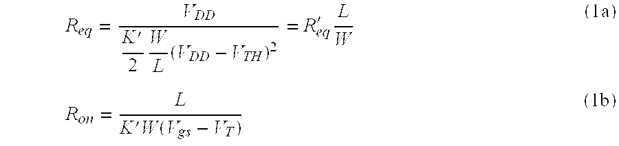
- wherein,
- L=FET channel length,
- W=FET channel width,
- R′ eq=is a constant dependent on the particular semiconductor process that is utilized.
- The equivalent capacitance for a digital FET can be shown to be:

- wherein,
- C ox is dependent on the gate oxide thickness of the digital FET.
- By substituting the expression for R eq and CLoad for the tDELAY equation:

-
Equation 3 can be solved for channel length to achieve a desired delay. Solving for a 104 pS delay results in channel length of L=0.62 um. Additionally, devices with a given length can be used in conjunction with a variable capacitive load to achieve a desired delay for a specific application. This will permit tuning of the filter. - As shown in Equation (3), the device width W is canceled out, and the device delay is largely independent of device width. Since the device delay is largely independent of device width, it is tempting to select minimum width devices to reduce layout area. Minimum width devices also result in lower power consumption due to a lower transconductance and lower current draw during moments of paralleled inverter output averaging. However, the
quadrature generator 600 relies on stage-to-stage matching to achieve high phase accuracy. The CMOS process can be characterized for device-to-device variations in threshold voltage, transconductance, and other parameters. In most cases improved parameter matching is achieved by increasing the device area. As a result, the FET channel width is increased to achieve the necessary device-to-device uniformity required to meet the phase imbalance specification. Larger devices require more layout area and also more power, as will be understood by those skilled in the arts. As a result, power consumption and layout area are being traded for phase accuracy. - FIG. 17 illustrates the tradeoff between phase error and FET size and current.
Curve 1702 depicts phase error vs. FET size, and illustrates that the phase error decreases as the FET size increases. Curve 1704 depicts drain current vs. FET size and illustrates that drain current increases with FET size. Therefore, in one embodiment, the FET size at 1706 is chosen as a compromise between low phase error and moderate power consumption. - It can be shown that a threshold voltage standard deviation/mean of about 1.8% would produce phase errors of less than 1 degree RMS. While a threshold voltage (V TH0) deviation can be assigned directly to the PSpice model, beta variations were included by allowing gate oxide thickness (tox) to vary. The variation of tox affects several parameters besides the transconductance (including threshold voltage), but provides a likely worst case analysis for phase sensitivity. A standard deviation/mean of 2% was assigned to tOX.
- The course quadrature signals are further refined with each correction stage. However, at some point the phase error will be limited by the component matching of the final stage, and additional stages provide little or no improvement in phase error. For example, the quadrature generator in FIG. 6 includes 4 refinement stages. The phase error is rapidly reduced to less than 2 degrees (from an initial 15-20 degrees) by the first two
stages third stage 606 c drops phase error to about 1.5 degrees, and the fourth stage provides enough improvement to the reduce phase error +/−1 degree, which is desired for one embodiment of the invention. - As discussed herein, the
delay circuits 802 and 702 are implemented using active inverter circuits, which can be implemented in standard semiconductor processes, such as CMOS. CMOS inverters on a common substrate have similar semiconductor characteristics that are repeatable from inverter-to-inverter, which improves the phase accuracy of the quadrature output signals. Furthermore, CMOS inverters are more area efficient than passive capacitors and passive resistors. Therefore, theentire quadrature generator 600 is more area efficient than theconventional delay circuit 500, which increases overall chip-yield. Similar concepts can be applied using ECL (emitter coupled logic) for the inverters with improved matching and accuracy. - FIG. 12 further illustrates the operation of
refinement stage 606. More specifically, FIG. 12 depicts a functional description of therefinement stage 606. Referring to FIG. 12, an input signal Vs 1208 is sub-divided into an in-phase signal 1206 and a quadrature signal 1212, producing anangle 1222 between the in-phase signal 1206 and the quadrature 1212. Due to the component inaccuracies in therefinement stage 606, theangle 1222 between the in-phase signal 1206 and the quadarature signal 1212 is not exactly 90 degrees, but is 90 degrees+/− some error. The in-phase signal 1206 is further sub-divided into an in-phase signal 1202 and aquadrature signal 1204, producing an angle 1220 between thesignals phase signal 1210 andquadrature signal 1216, producing anangle 1224 between thesignals angles 1220 and 1224 are also not exactly 90, and have substantially the same error as theangle 1222. The error is substantially the same because component inaccuracies are substantially the same in therefinement stage 606, due to the repeated use of inverters 906. - The in-
phase signals phase signal 1226. Likewise, thesignal 1218 is subtracted from thesignal 1216 to produce a combinedquadrature signal 1228. The combined in-phase signal 1226 is substantially in quadrature with the combinedquadrature signal 1228, so that the resultingangle 1230 is substantially 90 degrees, or at least has a final error component that is less than the error associated with theangles 1220 and 1224. The final error component is less because the corresponding inverters 906 in the 0/180 delay circuits are connected together. Therefore, any phase error signal at the output of the 0/180delay circuits 802 is averaged together and reduced. For example, the 0-degree output of the delay circuit 802-1 is connected together with the 180 degree output of the delay circuit 802-3. Since the delay circuit 802-3 has a 180 degree input 801-3, the 180 degree output of the delay circuit 802-3 should be at 0 degree, and in-phase with the 0-degree output of the 0/180 delay circuit 802-1. Likewise, the 180 degree output of the delay circuit 802-1 is connected to the 0-degree output of the delay circuit 802-3, to average any phase error at these outputs. The outputs of the delay circuits 802-2 and 802-4 are connected together in a similar manner, to average any phase error at their outputs. Likewise, the corresponding outputs of the 90/180 delay circuits 702 are also connected together to average any phase error at their respective outputs. - FIGS. 13A-C further describe the signal averaging performed by the connecting the outputs of the inverters 906 together. FIG. 13A illustrates substantially
identical inverters 906 a and 906 b that are output inverters of either a 0/180delay circuit 802, or are the output of a 90/180 delay circuit 702. For example, theinverter 906 a can be the output inverter 906 of the 0/180 degree delay circuit 802-1, and the inverter 906 b can be the output inverter 906 of the 0/180 degree delay circuit 802-3.Inverter 906 a has anoutput 1302 a and the inverter 906 b has an output 1302 b. Referring to FIG. 13C, eachoutput 1302 a and 1302 b has some phase error, but theoutput 1302 a leads the output 1302 b. - FIG. 13B illustrates the
inverters 906 a and 906 b having their outputs connected together at anoutput 1304. Referring again to FIG. 13C, theoutput 1304 is substantially an average of thesignals 1302 a and 1302 b, which reduces the phase error compared with theoutputs 1302 a and 1302 b. - Still referring to FIG. 13B, the
inverters 906 a and 906 b withcorresponding outputs 1302 a and 1302 b produce the averagedoutput 1304 when their respective outputs are tied together because of the source impedance and the load impedance of the inverters. Referring to FIG. 13D, eachinverter 906 a possesses a finite source impedance and it can be viewed that each inverter 906 drives a load impedance. Accordingly,VA,B Δ voltage at inverter outputs Z906A Δ output impedance of 906A inverter Z906B Δ output impedance of 906B inverter ZMI Δ branch impedance which may be distributed or lumped and may be related to passive or active circuitry associated with the load or matching networks ZM2 branch impedance which may be distributed or lumped and may be related to passive or active circuitry associated with the load or matching networks ZL Δ load impedance - The effective load from the perspective of
inverter 906 a is therefore; - ZLOAD-906A ΔZM1+ZL//ZM2
- Likewise, the effective load from the perspective of inverter 906 b is
- ZLOAD-906B ΔZM2+ZL//ZM1
- Now the voltages across Z L and the currents through ZL are proportioned to the outputs of the inverters and the values for Z906A,B and ZLOAD-906A,B. Therefore:

- This equation ( 3 a) indicates the transfer function in the frequency domain using Laplace transforms. The transient response my be obtained from the inverse Laplace transform. It is evident that VO can be manipulated by tailoring a number of items such as:
- a) voltage swing of each inverter which could be accomplished via varying the power supply and a host of other techniques,
- b) changing the inverter source impedances,
- c) changing branch impedances Z M1, ZM2,
- d) altering the load impedance.
- In summary, the averaging of the inverters 906 could be weighted equally or in an arbitrary manner. Furthermore, this weighting could be altered in situations to compensate for differing phase alignments. Moreover, N such circuits could be combined in parallel using the super position principles illustrated for the two branch circuit.
- FIG. 14 illustrates a
flowchart 1400 that further describes the operation of the refinement stages 606, and the phase error averaging performed by the refinement stages 606. - In step 1402, a first set of quadrature signals are received having some quadrature phase error. For example, referring to FIG. 8, input quadrature signals 801 a-801 d are received that have some quadrature phase error EIN.
- In
step 1404, a second set and a third set of quadrature signals are generated based on the first set of quadrature signals using inverters. The second set of quadrature signals are substantially in-phase with the first set of quadrature signals, and the third set of quadrature signals are substantially delayed by 180 degrees relative to the first set of quadrature signals. For example, 0-degree outputs of the 0/180delay circuits 802 are generated based on the first set of signals 801, and represent the second set of quadrature signals. The 0-degree outputs of thedelay circuit 802 are substantially in-phase with the inputs 801, and have a quadrature relationship with each other because the quadrature signals 801 have a quadrature relationship with each other. The 180 degree outputs of the 0/180delay circuits 802 are based on the first set of quadrature signals, and represent the third set of quadrature signals. The 180 degree outputs of the 0/180delay circuits 802 are substantially 180 degrees out of phase with the corresponding inputs 801. - In
step 1406, the second set of quadrature signals and the third set of quadrature signals are averaged together, to generate a fourth set of quadrature signals that have less phase error than the first set of quadrature signals. More specifically, corresponding signals of the second set of quadrature signals and the third set of quadrature signals are averaged together, to reduce the phase error in the fourth set of quadrature signals. For example, the 0-degree outputs of the 0/180delay circuits 802 are averaged with the corresponding 180 degree outputs of thedelay circuit 802 to generate averaged signals 804. For example, the 0 degree output of the 0/180 delay circuit 802-1 is averaged with the 180 degree output of the delay circuit 802-3, to generate an averaged signal 804-1 that is the input to the 90/180 degree delay circuit 702-1. Likewise, the 0-degree output of the delay circuit 802-2 is averaged with the 180 degree output of the delay circuit 802-4, to generate an averaged signal 804-2. Likewise, the 0-degree output of the delay circuit 802-3 is averaged with the 180 degree output of the delay circuit 802-1, to generate an averaged signal 804-3. Likewise, the 0-degree output of the delay circuit 802-4 is averaged with the 180 degree output of the delay circuit 802-2, to generate an averaged signal 804-4. - In step 1408, a fifth set and a sixth set of quadrature signals is generated based on the fourth set of quadrature signals. The fifth set of quadrature signals is delayed by 90 degrees relative to the fourth set of quadrature signals. The sixth set of quadrature signals is delayed by 180 degrees relative to the fourth set of quadrature signals, and therefore is delayed by 90 degrees relative to the fifth set of quadrature signals. For example, 90-degree outputs of the 90/180 delay circuits 702 represent the fifth set of quadrature signals, and are delayed by 90 degrees relative to the corresponding averaged signals 804-1 to 804-4. The 180 degree outputs of the 90/180 delay circuits 702 are also based on the fourth set of quadrature signals, and are delayed by 180 degrees relative to the corresponding averaged signals 804-1 to 804-4.
- In
step 1410, the fifth set of quadrature signals and the sixth set of quadrature signals are averaged together, to generate a seventh set of quadrature signals that have less phase error than the fourth set of quadrature signals. More specifically, corresponding signals of the fifth set of quadrature signals and the sixth set of quadrature signals are averaged together, to reduce the phase error in the seventh set of quadrature signals. For example, the 0-degree outputs of the 90/180 delay circuits 702 are averaged with the corresponding 180 degree outputs of the delay circuits 702, to generate averaged output signals 805. For example, the 90 degree output of the 90/180 delay circuit 702-1 is averaged with the 180 degree output of the delay circuit 702-3, to generate the quadrature output signal 805-1. Likewise, the 90-degree output of the delay circuit 702-2 is averaged with the 180 degree output of the delay circuit 702-1, to generate the quadrature output signal 805-2. Likewise, the 90-degree output of the delay circuit 702-3 is averaged with the 180 degree output of the delay circuit 702-4, to generate the quadrature output signal 804-3. Likewise, the 90-degree output of the delay circuit 702-4 is averaged with the 180 degree output of the delay circuit 702-3, to generate the quadrature output signal 805-4. - The phase error of the quadrature output signals 805 is less than the phase error of the quadrature input signals 801, due to the averaging performed by
steps 1406 and 1408. In embodiments, phase error is less than 1 degree at the frequency of interest. - 5. Mathematical Description
- A system level mathematical description of the operation of the
refinement stage 606 is given as follows. In order to facilitate the equation manipulation in the following description, the delay circuits 802-1 to 802-4 in FIG. 8 will be referred to as delay circuits A-1 to A-n, respectively. Likewise, the delay circuits 702-1 to 702-4 in FIG. 8 will be referred to as delay circuits B-1 to B-n. This is in accordance with the “A” placed over the row ofdelay circuit 802, and the “B” placed over the row of delay circuits 702 in FIG. 8. Furthermore, the input signals 801-1 to 801-4 will be referred to as in0, in90, in180, and in270, respectively. Furthermore, the output signals 805-1 through 805-4 will be referred to as out0, out90, out180, and out270. - The four input and output waveforms of the
refinement stage 606 can be approximately modeled as square waves although this is not strictly required. A Fourier decomposition can also be used to compare spectral components and their relative phases. The phase accuracy of therefinement stage 606 is measured by the relative time delay between rising or falling edges of each of the four output waveforms 805. Timing uncertainties result from input phase error and variability of propagation delay through each of thedelay circuit 802 and 702 of the refinement stages 606. A mathematical model is constructed and described below that preserves the individual timing errors and demonstrates the self-regulating nature of therefinement stage 606. - A unit rectangular pulse is defined as:

- Each of the input waveforms can be described by periodic rectangular pulse functions of fixed amplitude, A, and distinct timing with a periodicity of T, a pulse width of T/2, and first rising edge occurring at time t 0, as shown in FIG. 15. The equations for the input waveforms 801 based on this unit pulse description are as follows:

- wherein,
- in0 represents the 0 degree waveform 801-1,
- in90 represents the 90 degree waveform 801-2,
- in180 represents the 180 degree waveform 801-3, and
- in270 represents the 270 degree waveform 801-4.
- The primary function of each of the individual delay circuits A1-AN and B1-BN in FIG. 8 is to provide an approximate delay to each signal and combine the two hard-wired outputs, creating timing characteristics which are an average of the individual waveforms, where the averaging effect is shown in FIG. 13B. For example, the input to the delay circuit B- 1 comes from two hardwired outputs with inputs of in0 and in180 from the delay circuits A-1 and A-3, respectively. Assuming that in0 is defined as the zero degree reference, the timing of inB1 will be determined by the following:
- in-to-out0 propagation delay of the delay circuit A- 1 (where the delay is referenced as DA1:0 in the equations below)
- Timing uncertainties associated with in180 (where the timing is represented in t 180 in the equations below)
- in-to-out180 propagation delay of delay circuit A 3 (where the delay is referenced as DA3:180 in the equations below)
- The input signals and delays are viewed as random variables whose probability density functions (PDF) are uniformily distributed (in a worst case) over some range about their expected values or means. In some applications, the PDFs may be much more complex but the uniform assumption contemplates a worst case scenario of practical concern. Since components of the delays and waveforms are random variables, we may employ ideas from probability and statistics to address the method by which averaged phase values are obtained at the circuit output. For arbitrary PDFs associated with sums of random variables, the central limit theorm may be invoked to facilitate an understanding of how final averages or expected values of phases can be extracted.
- Understanding the periodic nature of the rectangular pulse function where a delay of integer periods (T) produces like timing and amplitudes, and dropping the amplitude (A), the out0 rising edge of the delay circuit A- 3 in FIG. 8 can be described in a modified notation as:
- A1out0=ΠRE(in0+DA1:0) (9)
- This represents a unity amplitude pulse whose rising edge occurs at a time determined by the input timing (i 0) and the effective delay through delay circuit A1(DA1:0), which in turn is related to the driving point and load impedances as well as the branch impedances of the circuit. Likewise, the other component of inB1 is derived from in180:
- A3out180=ΠRE(in180+DA3:180) (10)
- The hard-wired combination of these two signals is a unity amplitude pulse whose rising edge occurs at the average time of the two components. Also, since this is actually a periodic pulse with period T, the subtraction or addition of integer periods will not alter the edge timing, but assists in the analysis using the modified pulse notation. One period is subtracted from any single delay path which produces an approximate delay of 1 period (360 degrees) or more. The following expressions are therefore equivalent:
- A3out180=ΠRE(in180+DA3:180)=ΠRE(in180+DA3:180−T) (11)
- The input to the delay circuit B 1 can now be described as averaging A1out0 with A3out 180:

- This is a unit amplitude pulse whose rising edge occurs at a time:

- where:
- in0, in180=edge timing of the inputs in0 and in180
- DA1:0, DA3:180=propagation delay through the blocks A 1 and A3
- T=period of the input waveforms
- The timing associated with in180 would ideally be shifted by 180 degrees (T/2) from in 0. If in0 were defined as zero for an 800 MHz system:

- The actual timing of in180 will vary due to timing inaccuracies, noise, and temperature/process variations. Referring to FIG. 8, the inputs to each of the delay circuits in column B can be defined:

- Hard-wiring the appropriate outputs of the blocks in column B and time averaging the edge transitions produces the final outputs of the refinement stage, out0, out90, out180, and out270:

- In one embodiment, the out90 and out180 are random variables also since their components can be viewed as random variables. A significant number of processing stages will result in the observable possessing a Gaussian-like random variable which implies that the expected value is easily extracted by averaging, which also reduces the variance of the final estimate.
- Ideally, the time difference between rising edges of these two signals should be one fourth the period or 90 degrees. Subtracting the time difference between the 180 and 90 degree output results in:

- Assuming the delay circuits in column and column B are well matched (DA1:0=DA2:0=DA3:0=DA4:0 and DB1:0=DB2:0=DB3:0=DB4:0) and simplifying:

- Equation 22 indicates the relative phase between output signals 805 is substantially close to 90 degrees. The statistical mean of the result is a weak function of the initial phase error at the inputs 801. Furthermore, the result is also a statistical mean of individual delays through the
delay circuits 802 and 702 in FIG. 8. Whereas, conventional quadrature generators need to have identical delay circuits in order to produce perfect phase. From the equations above, it is seen that the timing imperfections (all inputs and delay blocks) that form the outputs are summed and averaged and applied equally to each output. Although the absolute delay from the input to the output of the refinement stage will still vary with temperature, process, etc., the difference in delays between adjacent outputs is forced to T/4 by the circuit architecture. - Furthermore, the
refinement stage 606 has a wide bandwidth since any of the individual delays (802 or 702) are not significant unless it affects the systems ability to perform waveform averaging. The ability to accurately perform averaging breaks down if the delay circuits are not in the neighborhood of the ideal delay. In one embodiment, for example, the bandwidth of a 4 stage 800 MHz quadrature generator was found to be over 500 MHz. Additional refinement stages can provide additional bandwidth. - FIG. 16 illustrates an example
LO generation circuit 1600, capable of generating quadrature pulsedcontrol signals 1614, based a differential input signal 1601. Adifferential amplifier 1602 receives the input signal 1601 and amplifies the input signal 1601, to generate an amplifiedsignal 1603. Thedifferential amplifier 1602 is included because the differential input signal 1601 can have a variable amplitude, and it is desirable to have aconstant amplitude signal 1603 during quadrature signal generation. A divide-by-twocircuit 1604 frequency divides the differential amplifiedsignal 1603 by two, to generate a frequency dividedsignal 1605. For example, in one embodiment, the differential input signal has a frequency of 1.6 GHz, and the divide by two circuit divides the frequency down to 800 MHz. A level-shift circuit 1606 DC level shifts thesignal 1605 to generate a level-shiftedoutput signal 1607 that is appropriate for thequadrature generator 600. Thequadrature generator 600 generatesquadrature signals 1609 based on the level-shiftedsignal 1607. Thepulse generator 1610 receives thesignals 1609, and generatesoutput pulses 1614 that have a quadrature relationship and have a desired pulse width. Thedifferential amplifier 1602 and the divide-by-twocircuit 1604 are biased using thebias regulator 1612. - The
output pulses 1614 can be used as the control signals 108 a-d that control the switches 126 in thebalanced modulator 100 of FIG. 1. The pulse width of theoutput pulses 1614 can be set to provide a desired sampling period for the switches 126 in thebalanced modulator 100 to improve energy transfer to a desired harmonic in the harmonicallyrich signal 103. - 6. Performance
- Operating on 800 MHz signals, the quadrature signal generator in FIG. 6 has shown to produce quadrature signals with less than +/−1 degree of phase error. Furthermore, the
quadrature generator 600 is also resistant to input phase error. Experiments have shown that the phase error can vary from +/−12 degrees, and the output phase error only varies from +/−150 milli-degree. Still further, thequadrature generator 600 is also resistant to input frequency error. Experiments have shown that the input frequency can vary can vary 1.2 GHz to 2.2 GHz, and the output phase error varies minimally. - 7. Conclusion
- Example embodiments of the methods, systems, and components of the present invention have been described herein. As noted elsewhere, these example embodiments have been described for illustrative purposes only, and are not limiting. Other embodiments are possible and are covered by the invention. Such other embodiments will be apparent to persons skilled in the relevant art(s) based on the teachings contained herein. Thus, the breadth and scope of the present invention should not be limited by any of the above-described exemplary embodiments, but should be defined only in accordance with the following claims and their equivalents.
Claims (22)
Priority Applications (1)
| Application Number | Priority Date | Filing Date | Title |
|---|---|---|---|
| US10/453,622 US7321640B2 (en) | 2002-06-07 | 2003-06-04 | Active polyphase inverter filter for quadrature signal generation |
Applications Claiming Priority (2)
| Application Number | Priority Date | Filing Date | Title |
|---|---|---|---|
| US38648402P | 2002-06-07 | 2002-06-07 | |
| US10/453,622 US7321640B2 (en) | 2002-06-07 | 2003-06-04 | Active polyphase inverter filter for quadrature signal generation |
Publications (2)
| Publication Number | Publication Date |
|---|---|
| US20030227983A1 true US20030227983A1 (en) | 2003-12-11 |
| US7321640B2 US7321640B2 (en) | 2008-01-22 |
Family
ID=29715426
Family Applications (1)
| Application Number | Title | Priority Date | Filing Date |
|---|---|---|---|
| US10/453,622 Expired - Fee Related US7321640B2 (en) | 2002-06-07 | 2003-06-04 | Active polyphase inverter filter for quadrature signal generation |
Country Status (1)
| Country | Link |
|---|---|
| US (1) | US7321640B2 (en) |
Cited By (7)
| Publication number | Priority date | Publication date | Assignee | Title |
|---|---|---|---|---|
| US20050159165A1 (en) * | 2004-01-15 | 2005-07-21 | Yiannis Argyropoulos | Method and apparatus for use in provisioning resources for a backhaul link |
| US7693230B2 (en) * | 1999-04-16 | 2010-04-06 | Parkervision, Inc. | Apparatus and method of differential IQ frequency up-conversion |
| WO2014088643A1 (en) | 2012-09-28 | 2014-06-12 | Intel Corporation | Distributed polyphase filter |
| US20140226700A1 (en) * | 2011-10-10 | 2014-08-14 | Rostyslav Volodymyrovych Bosenko | Wireless transmission system, method for wirelessly transmitting a data stream between a transmitting apparatus and a recening apparatus, method for wirelessly recening a signal, transmitting apparatus for wirelessly transmitting a data stream and recening apparatus for wirelessly recening two electric signals to produce a recened data stream |
| US9118528B2 (en) | 1998-10-21 | 2015-08-25 | Parkervision, Inc. | Method and system for down-converting an electromagnetic signal, and transforms for same, and aperture relationships |
| US20160094256A1 (en) * | 2014-09-30 | 2016-03-31 | Stmicroelectronics S.R.L. | System for the correction of the phase error of two in-phase and quadrature signals, corresponding device and method |
| CN111082778A (en) * | 2019-12-28 | 2020-04-28 | 西北工业大学 | Novel high image rejection ratio active CMOS (complementary Metal oxide semiconductor) multiphase filter circuit |
Families Citing this family (20)
| Publication number | Priority date | Publication date | Assignee | Title |
|---|---|---|---|---|
| US7515896B1 (en) | 1998-10-21 | 2009-04-07 | Parkervision, Inc. | Method and system for down-converting an electromagnetic signal, and transforms for same, and aperture relationships |
| US6370371B1 (en) | 1998-10-21 | 2002-04-09 | Parkervision, Inc. | Applications of universal frequency translation |
| US7236754B2 (en) * | 1999-08-23 | 2007-06-26 | Parkervision, Inc. | Method and system for frequency up-conversion |
| US7039372B1 (en) * | 1998-10-21 | 2006-05-02 | Parkervision, Inc. | Method and system for frequency up-conversion with modulation embodiments |
| US6853690B1 (en) * | 1999-04-16 | 2005-02-08 | Parkervision, Inc. | Method, system and apparatus for balanced frequency up-conversion of a baseband signal and 4-phase receiver and transceiver embodiments |
| US6879817B1 (en) | 1999-04-16 | 2005-04-12 | Parkervision, Inc. | DC offset, re-radiation, and I/Q solutions using universal frequency translation technology |
| US6873836B1 (en) * | 1999-03-03 | 2005-03-29 | Parkervision, Inc. | Universal platform module and methods and apparatuses relating thereto enabled by universal frequency translation technology |
| US7110435B1 (en) * | 1999-03-15 | 2006-09-19 | Parkervision, Inc. | Spread spectrum applications of universal frequency translation |
| US7110444B1 (en) | 1999-08-04 | 2006-09-19 | Parkervision, Inc. | Wireless local area network (WLAN) using universal frequency translation technology including multi-phase embodiments and circuit implementations |
| US7065162B1 (en) | 1999-04-16 | 2006-06-20 | Parkervision, Inc. | Method and system for down-converting an electromagnetic signal, and transforms for same |
| US8295406B1 (en) | 1999-08-04 | 2012-10-23 | Parkervision, Inc. | Universal platform module for a plurality of communication protocols |
| US7010286B2 (en) | 2000-04-14 | 2006-03-07 | Parkervision, Inc. | Apparatus, system, and method for down-converting and up-converting electromagnetic signals |
| US7454453B2 (en) * | 2000-11-14 | 2008-11-18 | Parkervision, Inc. | Methods, systems, and computer program products for parallel correlation and applications thereof |
| US7010559B2 (en) * | 2000-11-14 | 2006-03-07 | Parkervision, Inc. | Method and apparatus for a parallel correlator and applications thereof |
| US7072427B2 (en) * | 2001-11-09 | 2006-07-04 | Parkervision, Inc. | Method and apparatus for reducing DC offsets in a communication system |
| US7379883B2 (en) | 2002-07-18 | 2008-05-27 | Parkervision, Inc. | Networking methods and systems |
| US7460584B2 (en) | 2002-07-18 | 2008-12-02 | Parkervision, Inc. | Networking methods and systems |
| JP2016167781A (en) * | 2015-03-10 | 2016-09-15 | 富士通株式会社 | Radio communication device and method of controlling radio communication device |
| US9912324B2 (en) | 2015-09-01 | 2018-03-06 | International Business Machines Corporation | Open-loop quadrature clock corrector and generator |
| US10444785B2 (en) | 2018-03-15 | 2019-10-15 | Samsung Display Co., Ltd. | Compact and accurate quadrature clock generation circuits |
Citations (95)
| Publication number | Priority date | Publication date | Assignee | Title |
|---|---|---|---|---|
| US3719903A (en) * | 1971-06-25 | 1973-03-06 | Bell Telephone Labor Inc | Double sideband modem with either suppressed or transmitted carrier |
| US3737778A (en) * | 1967-05-13 | 1973-06-05 | Philips Nv | Device for the transmission of synchronous pulse signals |
| US3739282A (en) * | 1969-12-11 | 1973-06-12 | Licentia Gmbh | Radio receiver for single sideband reception |
| US4143322A (en) * | 1976-09-30 | 1979-03-06 | Nippon Electric Co., Ltd. | Carrier wave recovery system apparatus using synchronous detection |
| US4158149A (en) * | 1977-05-16 | 1979-06-12 | Hitachi Denshi Kabushiki Kaisha | Electronic switching circuit using junction type field-effect transistor |
| US4250458A (en) * | 1979-05-31 | 1981-02-10 | Digital Communications Corporation | Baseband DC offset detector and control circuit for DC coupled digital demodulator |
| US4286283A (en) * | 1979-12-20 | 1981-08-25 | Rca Corporation | Transcoder |
| US4380828A (en) * | 1981-05-26 | 1983-04-19 | Zenith Radio Corporation | UHF MOSFET Mixer |
| US4439787A (en) * | 1981-02-18 | 1984-03-27 | Sony Corporation | AFT Circuit |
| US4441080A (en) * | 1981-12-17 | 1984-04-03 | Bell Telephone Laboratories, Incorporated | Amplifier with controlled gain |
| US4591930A (en) * | 1983-09-23 | 1986-05-27 | Eastman Kodak Company | Signal processing for high resolution electronic still camera |
| US4811422A (en) * | 1986-12-22 | 1989-03-07 | Kahn Leonard R | Reduction of undesired harmonic components |
| US4814649A (en) * | 1987-12-18 | 1989-03-21 | Rockwell International Corporation | Dual gate FET mixing apparatus with feedback means |
| US4845389A (en) * | 1987-03-06 | 1989-07-04 | U.S. Philips Corporation | Very high frequency mixer |
| US4931716A (en) * | 1989-05-05 | 1990-06-05 | Milan Jovanovic | Constant frequency zero-voltage-switching multi-resonant converter |
| US5014130A (en) * | 1989-07-31 | 1991-05-07 | Siemens Aktiengesellschaft | Signal level control circuit having alternately switched capacitors in the feedback branch |
| US5131014A (en) * | 1991-04-19 | 1992-07-14 | General Instrument Corporation | Apparatus and method for recovery of multiphase modulated data |
| US5196806A (en) * | 1990-10-19 | 1993-03-23 | Nec Corporation | Output level control circuit for use in rf power amplifier |
| US5218562A (en) * | 1991-09-30 | 1993-06-08 | American Neuralogix, Inc. | Hamming data correlator having selectable word-length |
| US5239496A (en) * | 1989-12-27 | 1993-08-24 | Nynex Science & Technology, Inc. | Digital parallel correlator |
| US5390215A (en) * | 1992-10-13 | 1995-02-14 | Hughes Aircraft Company | Multi-processor demodulator for digital cellular base station employing partitioned demodulation procedure with pipelined execution |
| US5410270A (en) * | 1994-02-14 | 1995-04-25 | Motorola, Inc. | Differential amplifier circuit having offset cancellation and method therefor |
| US5410195A (en) * | 1991-10-31 | 1995-04-25 | Nec Corporation | Ripple-free phase detector using two sample-and-hold circuits |
| US5551076A (en) * | 1994-09-06 | 1996-08-27 | Motorola, Inc. | Circuit and method of series biasing a single-ended mixer |
| US5633610A (en) * | 1993-01-08 | 1997-05-27 | Sony Corporation | Monolithic microwave integrated circuit apparatus |
| US5634207A (en) * | 1995-02-13 | 1997-05-27 | Kabushiki Kaisha Toshiba | Frequency converter capable of reducing noise components in local oscillation signals |
| US5636140A (en) * | 1995-08-25 | 1997-06-03 | Advanced Micro Devices, Inc. | System and method for a flexible MAC layer interface in a wireless local area network |
| US5642071A (en) * | 1994-11-07 | 1997-06-24 | Alcatel N.V. | Transit mixer with current mode input |
| US5734683A (en) * | 1993-09-10 | 1998-03-31 | Nokia Mobile Phones Limited | Demodulation of an intermediate frequency signal by a sigma-delta converter |
| US5760629A (en) * | 1995-08-08 | 1998-06-02 | Matsushita Electric Industrial Co., Ltd. | DC offset compensation device |
| US5784689A (en) * | 1994-12-30 | 1998-07-21 | Nec Corporation | Output control circuit for transmission power amplifying circuit |
| US5787125A (en) * | 1996-05-06 | 1998-07-28 | Motorola, Inc. | Apparatus for deriving in-phase and quadrature-phase baseband signals from a communication signal |
| US5878088A (en) * | 1997-04-10 | 1999-03-02 | Thomson Consumer Electronics, Inc. | Digital variable symbol timing recovery system for QAM |
| US5884154A (en) * | 1996-06-26 | 1999-03-16 | Raytheon Company | Low noise mixer circuit having passive inductor elements |
| US5887001A (en) * | 1995-12-13 | 1999-03-23 | Bull Hn Information Systems Inc. | Boundary scan architecture analog extension with direct connections |
| US5896347A (en) * | 1996-12-27 | 1999-04-20 | Fujitsu Limited | Semiconductor memory system using a clock-synchronous semiconductor device and semiconductor memory device for use in the same |
| US5896304A (en) * | 1996-07-12 | 1999-04-20 | General Electric Company | Low power parallel correlator for measuring correlation between digital signal segments |
| US5900746A (en) * | 1996-06-13 | 1999-05-04 | Texas Instruments Incorporated | Ultra low jitter differential to fullswing BiCMOS comparator with equal rise/fall time and complementary outputs |
| US5918167A (en) * | 1997-03-11 | 1999-06-29 | Northern Telecom Limited | Quadrature downconverter local oscillator leakage canceller |
| US6057714A (en) * | 1998-05-29 | 2000-05-02 | Conexant Systems, Inc. | Double balance differential active ring mixer with current shared active input balun |
| US6064054A (en) * | 1995-08-21 | 2000-05-16 | Diasense, Inc. | Synchronous detection for photoconductive detectors |
| US6084465A (en) * | 1998-05-04 | 2000-07-04 | Tritech Microelectronics, Ltd. | Method for time constant tuning of gm-C filters |
| US6182011B1 (en) * | 1996-04-01 | 2001-01-30 | The United States Of America As Represented By The Administrator Of National Aeronautics And Space Administration | Method and apparatus for determining position using global positioning satellites |
| US6204789B1 (en) * | 1999-09-06 | 2001-03-20 | Kabushiki Kaisha Toshiba | Variable resistor circuit and a digital-to-analog converter |
| US6208636B1 (en) * | 1998-05-28 | 2001-03-27 | Northpoint Technology, Ltd. | Apparatus and method for processing signals selected from multiple data streams |
| US6212369B1 (en) * | 1998-06-05 | 2001-04-03 | Maxim Integrated Products, Inc. | Merged variable gain mixers |
| US6211718B1 (en) * | 1997-01-11 | 2001-04-03 | Motel Semiconductor Limited | Low voltage double balanced mixer |
| US6215828B1 (en) * | 1996-02-10 | 2001-04-10 | Telefonaktiebolaget Lm Ericsson (Publ) | Signal transformation method and apparatus |
| USRE37138E1 (en) * | 1988-09-19 | 2001-04-17 | Telefonaktiebolaget Lm Ericsson | Log-polar signal processing |
| US6246695B1 (en) * | 1995-06-21 | 2001-06-12 | Bell Atlantic Network Services, Inc. | Variable rate and variable mode transmission system |
| US6259293B1 (en) * | 1999-06-15 | 2001-07-10 | Mitsubishi Denki Kabushiki Kaisha | Delay circuitry, clock generating circuitry, and phase synchronization circuitry |
| US20010015673A1 (en) * | 1999-12-28 | 2001-08-23 | Kazuo Yamashita | Feed-forward amplifier and controller of the same |
| US6335656B1 (en) * | 1999-09-30 | 2002-01-01 | Analog Devices, Inc. | Direct conversion receivers and filters adapted for use therein |
| US6366622B1 (en) * | 1998-12-18 | 2002-04-02 | Silicon Wave, Inc. | Apparatus and method for wireless communications |
| US6385439B1 (en) * | 1997-10-31 | 2002-05-07 | Telefonaktiebolaget Lm Ericsson (Publ) | Linear RF power amplifier with optically activated switches |
| US6393070B1 (en) * | 1997-08-12 | 2002-05-21 | Koninklijke Philips Electronics N.V. | Digital communication device and a mixer |
| US6404758B1 (en) * | 1999-04-19 | 2002-06-11 | Ericsson, Inc. | System and method for achieving slot synchronization in a wideband CDMA system in the presence of large initial frequency errors |
| US6404823B1 (en) * | 1998-07-01 | 2002-06-11 | Conexant Systems, Inc. | Envelope feedforward technique with power control for efficient linear RF power amplification |
| US20020080728A1 (en) * | 2000-11-03 | 2002-06-27 | Sugar Gary L. | Wideband multi-protocol wireless radio transceiver system |
| US6438366B1 (en) * | 1998-05-29 | 2002-08-20 | Nokia Mobile Phones Limited | Method and circuit for sampling a signal at high sampling frequency |
| US6441659B1 (en) * | 1999-04-30 | 2002-08-27 | Mosaid Technologies Incorporated | Frequency-doubling delay locked loop |
| US6441694B1 (en) * | 2000-12-15 | 2002-08-27 | Motorola, Inc. | Method and apparatus for generating digitally modulated signals |
| US6509777B2 (en) * | 2001-01-23 | 2003-01-21 | Resonext Communications, Inc. | Method and apparatus for reducing DC offset |
| US6512544B1 (en) * | 1998-06-17 | 2003-01-28 | Foveon, Inc. | Storage pixel sensor and array with compression |
| US20030045263A1 (en) * | 2000-11-29 | 2003-03-06 | Myles Wakayama | Integrated direct conversion satellite tuner |
| US20030081781A1 (en) * | 1994-03-31 | 2003-05-01 | Jensen James M. | Apparatus and methods for including codes in audio signals |
| US6560451B1 (en) * | 1999-10-15 | 2003-05-06 | Cirrus Logic, Inc. | Square wave analog multiplier |
| US6591310B1 (en) * | 2000-05-11 | 2003-07-08 | Lsi Logic Corporation | Method of responding to I/O request and associated reply descriptor |
| US6597240B1 (en) * | 2001-04-02 | 2003-07-22 | Cirrus Logic, Inc. | Circuits and methods for slew rate control and current limiting in switch-mode systems |
| US6600795B1 (en) * | 1994-11-30 | 2003-07-29 | Matsushita Electric Industrial Co., Ltd. | Receiving circuit |
| US6690232B2 (en) * | 2001-09-27 | 2004-02-10 | Kabushiki Kaisha Toshiba | Variable gain amplifier |
| US6741139B2 (en) * | 2001-05-22 | 2004-05-25 | Ydi Wirelesss, Inc. | Optical to microwave converter using direct modulation phase shift keying |
| US6741650B1 (en) * | 2000-03-02 | 2004-05-25 | Adc Telecommunications, Inc. | Architecture for intermediate frequency encoder |
| US6850742B2 (en) * | 2001-06-01 | 2005-02-01 | Sige Semiconductor Inc. | Direct conversion receiver |
| US6853690B1 (en) * | 1999-04-16 | 2005-02-08 | Parkervision, Inc. | Method, system and apparatus for balanced frequency up-conversion of a baseband signal and 4-phase receiver and transceiver embodiments |
| US6865399B2 (en) * | 2000-10-26 | 2005-03-08 | Renesas Technology Corp. | Mobile telephone apparatus |
| US6873836B1 (en) * | 1999-03-03 | 2005-03-29 | Parkervision, Inc. | Universal platform module and methods and apparatuses relating thereto enabled by universal frequency translation technology |
| US6879817B1 (en) * | 1999-04-16 | 2005-04-12 | Parkervision, Inc. | DC offset, re-radiation, and I/Q solutions using universal frequency translation technology |
| US6882194B2 (en) * | 2002-02-15 | 2005-04-19 | Stmicroelectronics S.A. | Class AB differential mixer |
| US6892062B2 (en) * | 2000-06-02 | 2005-05-10 | Information And Communications University Educational Foundation | Current-reuse bleeding mixer |
| US6892057B2 (en) * | 2002-08-08 | 2005-05-10 | Telefonaktiebolaget Lm Ericsson (Publ) | Method and apparatus for reducing dynamic range of a power amplifier |
| US6910015B2 (en) * | 2000-03-29 | 2005-06-21 | Sony Corporation | Sales activity management system, sales activity management apparatus, and sales activity management method |
| US6909739B1 (en) * | 1999-10-13 | 2005-06-21 | U-Nav Microelectronics Corporation | Signal acquisition system for spread spectrum receiver |
| US6917796B2 (en) * | 2001-10-04 | 2005-07-12 | Scientific Components | Triple balanced mixer |
| US6920311B2 (en) * | 1999-10-21 | 2005-07-19 | Broadcom Corporation | Adaptive radio transceiver with floating MOSFET capacitors |
| US20060039449A1 (en) * | 1997-05-16 | 2006-02-23 | Fontana Robert J | Ultra-wideband receiver and transmitter |
| US7006805B1 (en) * | 1999-01-22 | 2006-02-28 | Parker Vision, Inc. | Aliasing communication system with multi-mode and multi-band functionality and embodiments thereof, such as the family radio service |
| US7010286B2 (en) * | 2000-04-14 | 2006-03-07 | Parkervision, Inc. | Apparatus, system, and method for down-converting and up-converting electromagnetic signals |
| US7010559B2 (en) * | 2000-11-14 | 2006-03-07 | Parkervision, Inc. | Method and apparatus for a parallel correlator and applications thereof |
| US7016663B2 (en) * | 1998-10-21 | 2006-03-21 | Parkervision, Inc. | Applications of universal frequency translation |
| US7027786B1 (en) * | 1998-10-21 | 2006-04-11 | Parkervision, Inc. | Carrier and clock recovery using universal frequency translation |
| US7039372B1 (en) * | 1998-10-21 | 2006-05-02 | Parkervision, Inc. | Method and system for frequency up-conversion with modulation embodiments |
| US7072433B2 (en) * | 2001-07-11 | 2006-07-04 | Micron Technology, Inc. | Delay locked loop fine tune |
| US7194246B2 (en) * | 1998-10-21 | 2007-03-20 | Parkervision, Inc. | Methods and systems for down-converting a signal using a complementary transistor structure |
| US7209725B1 (en) * | 1999-01-22 | 2007-04-24 | Parkervision, Inc | Analog zero if FM decoder and embodiments thereof, such as the family radio service |
Family Cites Families (91)
| Publication number | Priority date | Publication date | Assignee | Title |
|---|---|---|---|---|
| US2057613A (en) | 1932-07-28 | 1936-10-13 | Gen Electric | Diversity factor receiving system |
| US2241078A (en) | 1937-11-01 | 1941-05-06 | Frederick K Vreeland | Multiplex communication |
| US2283575A (en) | 1938-04-19 | 1942-05-19 | Rca Corp | High frequency transmission system |
| GB519264A (en) | 1938-10-10 | 1940-03-20 | Philips Nv | Improvements in or relating to multi-carrier transmission systems |
| GB556208A (en) | 1941-04-25 | 1943-09-24 | Standard Telephones Cables Ltd | Arrangement for conversion of frequency modulation to phase modulation and the application thereof to the production of a frequency modulated wave from a frequency stable oscillator |
| US2462069A (en) | 1942-05-07 | 1949-02-22 | Int Standard Electric Corp | Radio communication system |
| US2410350A (en) | 1943-02-06 | 1946-10-29 | Standard Telephones Cables Ltd | Method and means for communication |
| US2472798A (en) | 1943-11-29 | 1949-06-14 | Rca Corp | Low-pass filter system |
| US2462181A (en) | 1944-09-28 | 1949-02-22 | Western Electric Co | Radio transmitting system |
| US2451430A (en) | 1946-04-23 | 1948-10-12 | Jefferson Standard Broadcastin | Carrier frequency shift signaling |
| BE473802A (en) | 1946-08-20 | |||
| GB651011A (en) | 1947-04-22 | 1951-03-07 | Ericsson Telefon Ab L M | Improvements in modulation devices particularly for wide frequency bands |
| US2497859A (en) | 1947-11-19 | 1950-02-21 | Western Union Telegraph Co | Frequency diversity telegraph system |
| US2802208A (en) | 1952-06-25 | 1957-08-06 | Charles F Hobbs | Radio frequency multiplexing |
| US2985875A (en) | 1958-02-12 | 1961-05-23 | Marconi Wireless Telegraph Co | Radio communication systems |
| US3069679A (en) | 1959-04-22 | 1962-12-18 | Westinghouse Electric Corp | Multiplex communication systems |
| NL257346A (en) | 1959-10-30 | |||
| US3246084A (en) | 1960-08-26 | 1966-04-12 | Bolt Beranek & Newman | Method of and apparatus for speech compression and the like |
| US3114106A (en) | 1960-11-23 | 1963-12-10 | Mcmauus Robert Paul | Frequency diversity system |
| US3023309A (en) | 1960-12-19 | 1962-02-27 | Bell Telephone Labor Inc | Communication system |
| US3104393A (en) | 1961-10-18 | 1963-09-17 | Joseph H Vogelman | Method and apparatus for phase and amplitude control in ionospheric communications systems |
| US3226643A (en) | 1962-01-08 | 1965-12-28 | Avco Corp | Command communication system of the rectangular wave type |
| US3258694A (en) | 1964-01-03 | 1966-06-28 | Multi-channel p.m. transmitter with automatic modulation index control | |
| US3384822A (en) | 1964-03-21 | 1968-05-21 | Nippon Electric Co | Frequency-shift-keying phase-modulation code transmission system |
| US3383598A (en) | 1965-02-15 | 1968-05-14 | Space General Corp | Transmitter for multiplexed phase modulated singaling system |
| FR1504609A (en) | 1966-09-21 | 1967-12-08 | Ibm France | Data transmission system |
| US3454718A (en) | 1966-10-03 | 1969-07-08 | Xerox Corp | Fsk transmitter with transmission of the same number of cycles of each carrier frequency |
| US3555428A (en) | 1966-10-03 | 1971-01-12 | Xerox Corp | Fsk receiver for detecting a data signal with the same number of cycles of each carrier frequency |
| US3617892A (en) | 1967-02-27 | 1971-11-02 | Rca Corp | Frequency modulation system for spreading radiated power |
| CH497089A (en) | 1968-07-26 | 1970-09-30 | Autophon Ag | System for the transmission of continuous signals |
| US3629696A (en) | 1968-08-06 | 1971-12-21 | Northeast Electronics Corp | Method and apparatus for measuring delay distortion including simultaneously applied modulated signals |
| US3614627A (en) | 1968-10-15 | 1971-10-19 | Data Control Systems Inc | Universal demodulation system |
| US3548342A (en) | 1968-10-15 | 1970-12-15 | Ibm | Digitally controlled amplitude modulation circuit |
| US3614630A (en) | 1969-02-04 | 1971-10-19 | Develco | Radio frequency standard and voltage controlled oscillator |
| US3626417A (en) | 1969-03-07 | 1971-12-07 | Everett A Gilbert | Hybrid frequency shift-amplitude modulated tone system |
| FR2040580A5 (en) | 1969-04-03 | 1971-01-22 | Inst Francais Du Petrole | |
| US3617898A (en) | 1969-04-09 | 1971-11-02 | Eugene A Janning Jr | Orthogonal passive frequency converter with control port and signal port |
| US3767984A (en) | 1969-09-03 | 1973-10-23 | Nippon Electric Co | Schottky barrier type field effect transistor |
| US3623160A (en) | 1969-09-17 | 1971-11-23 | Sanders Associates Inc | Data modulator employing sinusoidal synthesis |
| US3641442A (en) | 1970-06-25 | 1972-02-08 | Hughes Aircraft Co | Digital frequency synthesizer |
| US3621402A (en) | 1970-08-03 | 1971-11-16 | Bell Telephone Labor Inc | Sampled data filter |
| US3689841A (en) | 1970-10-23 | 1972-09-05 | Signatron | Communication system for eliminating time delay effects when used in a multipath transmission medium |
| US3702440A (en) | 1970-11-16 | 1972-11-07 | Motorola Inc | Selective calling system providing an increased number of calling codes or auxiliary information transfer |
| US3662268A (en) | 1970-11-17 | 1972-05-09 | Bell Telephone Labor Inc | Diversity communication system using distinct spectral arrangements for each branch |
| US3694754A (en) | 1970-12-28 | 1972-09-26 | Tracor | Suppression of electrostatic noise in antenna systems |
| US3716730A (en) | 1971-04-19 | 1973-02-13 | Motorola Inc | Intermodulation rejection capabilities of field-effect transistor radio frequency amplifiers and mixers |
| US3714577A (en) | 1971-05-06 | 1973-01-30 | W Hayes | Single sideband am-fm modulation system |
| US3736513A (en) | 1971-06-28 | 1973-05-29 | Warwick Electronics Inc | Receiver tuning system |
| US3764921A (en) | 1972-10-27 | 1973-10-09 | Control Data Corp | Sample and hold circuit |
| US3852530A (en) | 1973-03-19 | 1974-12-03 | M Shen | Single stage power amplifiers for multiple signal channels |
| US4066841A (en) | 1974-01-25 | 1978-01-03 | Serck Industries Limited | Data transmitting systems |
| JPS5113208U (en) | 1974-07-17 | 1976-01-30 | ||
| US4035732A (en) | 1974-10-03 | 1977-07-12 | The United States Of America As Represented By The Secretary Of The Army | High dynamic range receiver front end mixer requiring low local oscillator injection power |
| US3940697A (en) | 1974-12-02 | 1976-02-24 | Hy-Gain Electronics Corporation | Multiple band scanning radio |
| US4017798A (en) | 1975-09-08 | 1977-04-12 | Ncr Corporation | Spread spectrum demodulator |
| US4047121A (en) | 1975-10-16 | 1977-09-06 | The United States Of America As Represented By The Secretary Of The Navy | RF signal generator |
| US4013966A (en) | 1975-10-16 | 1977-03-22 | The United States Of America As Represented By The Secretary Of The Navy | Fm rf signal generator using step recovery diode |
| US4019140A (en) | 1975-10-24 | 1977-04-19 | Bell Telephone Laboratories, Incorporated | Methods and apparatus for reducing intelligible crosstalk in single sideband radio systems |
| US4045740A (en) | 1975-10-28 | 1977-08-30 | The United States Of America As Represented By The Secretary Of The Army | Method for optimizing the bandwidth of a radio receiver |
| JPS5823978B2 (en) | 1975-11-11 | 1983-05-18 | ソニー株式会社 | Chuyuna |
| JPS5826699B2 (en) | 1975-11-13 | 1983-06-04 | ソニー株式会社 | Chuyuna |
| US4032847A (en) | 1976-01-05 | 1977-06-28 | Raytheon Company | Distortion adapter receiver having intersymbol interference correction |
| US4066919A (en) | 1976-04-01 | 1978-01-03 | Motorola, Inc. | Sample and hold circuit |
| JPS52141113A (en) | 1976-05-19 | 1977-11-25 | Nippon Telegr & Teleph Corp <Ntt> | Transmission diversity system |
| NL175575C (en) | 1976-05-28 | 1984-11-16 | Philips Nv | FILTER AND DEMODULATION DEVICE. |
| US4081748A (en) | 1976-07-01 | 1978-03-28 | Northern Illinois Gas Company | Frequency/space diversity data transmission system |
| US4080573A (en) | 1976-07-16 | 1978-03-21 | Motorola, Inc. | Balanced mixer using complementary devices |
| US4051475A (en) | 1976-07-21 | 1977-09-27 | The United States Ofamerica As Represented By The Secretary Of The Army | Radio receiver isolation system |
| US4130765A (en) | 1977-05-31 | 1978-12-19 | Rafi Arakelian | Low supply voltage frequency multiplier with common base transistor amplifier |
| US4346477A (en) | 1977-08-01 | 1982-08-24 | E-Systems, Inc. | Phase locked sampling radio receiver |
| JPS5461822A (en) | 1977-10-27 | 1979-05-18 | Sony Corp | Transmitter circuit |
| US4170764A (en) | 1978-03-06 | 1979-10-09 | Bell Telephone Laboratories, Incorporated | Amplitude and frequency modulation system |
| DE2813946C2 (en) | 1978-03-31 | 1980-01-31 | Siemens Ag, 1000 Berlin Und 8000 Muenchen | Filter circuit with a biquadratic transfer function |
| US4204171A (en) | 1978-05-30 | 1980-05-20 | Rca Corporation | Filter which tracks changing frequency of input signal |
| US4241451A (en) | 1978-06-26 | 1980-12-23 | Rockwell International Corporation | Single sideband signal demodulator |
| US4193036A (en) | 1978-07-03 | 1980-03-11 | Motorola, Inc. | Balanced active mixer circuit |
| US4210872A (en) | 1978-09-08 | 1980-07-01 | American Microsystems, Inc. | High pass switched capacitor filter section |
| US4308614A (en) | 1978-10-26 | 1981-12-29 | Fisher Charles B | Noise-reduction sampling system |
| US4253067A (en) | 1978-12-11 | 1981-02-24 | Rockwell International Corporation | Baseband differentially phase encoded radio signal detector |
| US4320361A (en) | 1979-07-20 | 1982-03-16 | Marconi Instruments Limited | Amplitude and frequency modulators using a switchable component controlled by data signals |
| US4245355A (en) | 1979-08-08 | 1981-01-13 | Eaton Corporation | Microwave frequency converter |
| US4320536A (en) | 1979-09-18 | 1982-03-16 | Dietrich James L | Subharmonic pumped mixer circuit |
| JPS5648732A (en) | 1979-09-28 | 1981-05-02 | Nec Corp | Radio equipment |
| FR2471081B1 (en) | 1979-11-30 | 1986-05-30 | Thomson Csf | SWITCHED CAPACITY FILTER WITH LOAD TRANSFER |
| US4356558A (en) | 1979-12-20 | 1982-10-26 | Martin Marietta Corporation | Optimum second order digital filter |
| US4370572A (en) | 1980-01-17 | 1983-01-25 | Trw Inc. | Differential sample-and-hold circuit |
| FR2474791A1 (en) | 1980-01-29 | 1981-07-31 | Thomson Csf | DIVERSITY RADIO-TRANSMISSION SYSTEM OF SIMPLE AND ECONOMIC STRUCTURE, AND TELECOMMUNICATION NETWORK COMPRISING SUCH SYSTEMS |
| US4253066A (en) | 1980-05-13 | 1981-02-24 | Fisher Charles B | Synchronous detection with sampling |
| US4334324A (en) | 1980-10-31 | 1982-06-08 | Rca Corporation | Complementary symmetry FET frequency converter circuits |
| US4360867A (en) | 1980-12-08 | 1982-11-23 | Bell Telephone Laboratories, Incorporated | Broadband frequency multiplication by multitransition operation of step recovery diode |
| US4384357A (en) | 1981-04-03 | 1983-05-17 | Canadian Patens & Development Limited | Self-synchronization circuit for a FFSK or MSK demodulator |
-
2003
- 2003-06-04 US US10/453,622 patent/US7321640B2/en not_active Expired - Fee Related
Patent Citations (99)
| Publication number | Priority date | Publication date | Assignee | Title |
|---|---|---|---|---|
| US3737778A (en) * | 1967-05-13 | 1973-06-05 | Philips Nv | Device for the transmission of synchronous pulse signals |
| US3739282A (en) * | 1969-12-11 | 1973-06-12 | Licentia Gmbh | Radio receiver for single sideband reception |
| US3719903A (en) * | 1971-06-25 | 1973-03-06 | Bell Telephone Labor Inc | Double sideband modem with either suppressed or transmitted carrier |
| US4143322A (en) * | 1976-09-30 | 1979-03-06 | Nippon Electric Co., Ltd. | Carrier wave recovery system apparatus using synchronous detection |
| US4158149A (en) * | 1977-05-16 | 1979-06-12 | Hitachi Denshi Kabushiki Kaisha | Electronic switching circuit using junction type field-effect transistor |
| US4250458A (en) * | 1979-05-31 | 1981-02-10 | Digital Communications Corporation | Baseband DC offset detector and control circuit for DC coupled digital demodulator |
| US4286283A (en) * | 1979-12-20 | 1981-08-25 | Rca Corporation | Transcoder |
| US4439787A (en) * | 1981-02-18 | 1984-03-27 | Sony Corporation | AFT Circuit |
| US4380828A (en) * | 1981-05-26 | 1983-04-19 | Zenith Radio Corporation | UHF MOSFET Mixer |
| US4441080A (en) * | 1981-12-17 | 1984-04-03 | Bell Telephone Laboratories, Incorporated | Amplifier with controlled gain |
| US4591930A (en) * | 1983-09-23 | 1986-05-27 | Eastman Kodak Company | Signal processing for high resolution electronic still camera |
| US4811422A (en) * | 1986-12-22 | 1989-03-07 | Kahn Leonard R | Reduction of undesired harmonic components |
| US4845389A (en) * | 1987-03-06 | 1989-07-04 | U.S. Philips Corporation | Very high frequency mixer |
| US4814649A (en) * | 1987-12-18 | 1989-03-21 | Rockwell International Corporation | Dual gate FET mixing apparatus with feedback means |
| USRE37138E1 (en) * | 1988-09-19 | 2001-04-17 | Telefonaktiebolaget Lm Ericsson | Log-polar signal processing |
| US4931716A (en) * | 1989-05-05 | 1990-06-05 | Milan Jovanovic | Constant frequency zero-voltage-switching multi-resonant converter |
| US5014130A (en) * | 1989-07-31 | 1991-05-07 | Siemens Aktiengesellschaft | Signal level control circuit having alternately switched capacitors in the feedback branch |
| US5239496A (en) * | 1989-12-27 | 1993-08-24 | Nynex Science & Technology, Inc. | Digital parallel correlator |
| US5196806A (en) * | 1990-10-19 | 1993-03-23 | Nec Corporation | Output level control circuit for use in rf power amplifier |
| US5131014A (en) * | 1991-04-19 | 1992-07-14 | General Instrument Corporation | Apparatus and method for recovery of multiphase modulated data |
| US5218562A (en) * | 1991-09-30 | 1993-06-08 | American Neuralogix, Inc. | Hamming data correlator having selectable word-length |
| US5410195A (en) * | 1991-10-31 | 1995-04-25 | Nec Corporation | Ripple-free phase detector using two sample-and-hold circuits |
| US5390215A (en) * | 1992-10-13 | 1995-02-14 | Hughes Aircraft Company | Multi-processor demodulator for digital cellular base station employing partitioned demodulation procedure with pipelined execution |
| US5633610A (en) * | 1993-01-08 | 1997-05-27 | Sony Corporation | Monolithic microwave integrated circuit apparatus |
| US5734683A (en) * | 1993-09-10 | 1998-03-31 | Nokia Mobile Phones Limited | Demodulation of an intermediate frequency signal by a sigma-delta converter |
| US5410270A (en) * | 1994-02-14 | 1995-04-25 | Motorola, Inc. | Differential amplifier circuit having offset cancellation and method therefor |
| US20030081781A1 (en) * | 1994-03-31 | 2003-05-01 | Jensen James M. | Apparatus and methods for including codes in audio signals |
| US5551076A (en) * | 1994-09-06 | 1996-08-27 | Motorola, Inc. | Circuit and method of series biasing a single-ended mixer |
| US5642071A (en) * | 1994-11-07 | 1997-06-24 | Alcatel N.V. | Transit mixer with current mode input |
| US6600795B1 (en) * | 1994-11-30 | 2003-07-29 | Matsushita Electric Industrial Co., Ltd. | Receiving circuit |
| US5784689A (en) * | 1994-12-30 | 1998-07-21 | Nec Corporation | Output control circuit for transmission power amplifying circuit |
| US5634207A (en) * | 1995-02-13 | 1997-05-27 | Kabushiki Kaisha Toshiba | Frequency converter capable of reducing noise components in local oscillation signals |
| US6246695B1 (en) * | 1995-06-21 | 2001-06-12 | Bell Atlantic Network Services, Inc. | Variable rate and variable mode transmission system |
| US5760629A (en) * | 1995-08-08 | 1998-06-02 | Matsushita Electric Industrial Co., Ltd. | DC offset compensation device |
| US6064054A (en) * | 1995-08-21 | 2000-05-16 | Diasense, Inc. | Synchronous detection for photoconductive detectors |
| US5636140A (en) * | 1995-08-25 | 1997-06-03 | Advanced Micro Devices, Inc. | System and method for a flexible MAC layer interface in a wireless local area network |
| US5887001A (en) * | 1995-12-13 | 1999-03-23 | Bull Hn Information Systems Inc. | Boundary scan architecture analog extension with direct connections |
| US6215828B1 (en) * | 1996-02-10 | 2001-04-10 | Telefonaktiebolaget Lm Ericsson (Publ) | Signal transformation method and apparatus |
| US6182011B1 (en) * | 1996-04-01 | 2001-01-30 | The United States Of America As Represented By The Administrator Of National Aeronautics And Space Administration | Method and apparatus for determining position using global positioning satellites |
| US5787125A (en) * | 1996-05-06 | 1998-07-28 | Motorola, Inc. | Apparatus for deriving in-phase and quadrature-phase baseband signals from a communication signal |
| US5900746A (en) * | 1996-06-13 | 1999-05-04 | Texas Instruments Incorporated | Ultra low jitter differential to fullswing BiCMOS comparator with equal rise/fall time and complementary outputs |
| US5884154A (en) * | 1996-06-26 | 1999-03-16 | Raytheon Company | Low noise mixer circuit having passive inductor elements |
| US5896304A (en) * | 1996-07-12 | 1999-04-20 | General Electric Company | Low power parallel correlator for measuring correlation between digital signal segments |
| US5896347A (en) * | 1996-12-27 | 1999-04-20 | Fujitsu Limited | Semiconductor memory system using a clock-synchronous semiconductor device and semiconductor memory device for use in the same |
| US6211718B1 (en) * | 1997-01-11 | 2001-04-03 | Motel Semiconductor Limited | Low voltage double balanced mixer |
| US5918167A (en) * | 1997-03-11 | 1999-06-29 | Northern Telecom Limited | Quadrature downconverter local oscillator leakage canceller |
| US5878088A (en) * | 1997-04-10 | 1999-03-02 | Thomson Consumer Electronics, Inc. | Digital variable symbol timing recovery system for QAM |
| US20060039449A1 (en) * | 1997-05-16 | 2006-02-23 | Fontana Robert J | Ultra-wideband receiver and transmitter |
| US6393070B1 (en) * | 1997-08-12 | 2002-05-21 | Koninklijke Philips Electronics N.V. | Digital communication device and a mixer |
| US6385439B1 (en) * | 1997-10-31 | 2002-05-07 | Telefonaktiebolaget Lm Ericsson (Publ) | Linear RF power amplifier with optically activated switches |
| US6084465A (en) * | 1998-05-04 | 2000-07-04 | Tritech Microelectronics, Ltd. | Method for time constant tuning of gm-C filters |
| US6208636B1 (en) * | 1998-05-28 | 2001-03-27 | Northpoint Technology, Ltd. | Apparatus and method for processing signals selected from multiple data streams |
| US6438366B1 (en) * | 1998-05-29 | 2002-08-20 | Nokia Mobile Phones Limited | Method and circuit for sampling a signal at high sampling frequency |
| US6057714A (en) * | 1998-05-29 | 2000-05-02 | Conexant Systems, Inc. | Double balance differential active ring mixer with current shared active input balun |
| US6212369B1 (en) * | 1998-06-05 | 2001-04-03 | Maxim Integrated Products, Inc. | Merged variable gain mixers |
| US6512544B1 (en) * | 1998-06-17 | 2003-01-28 | Foveon, Inc. | Storage pixel sensor and array with compression |
| US6404823B1 (en) * | 1998-07-01 | 2002-06-11 | Conexant Systems, Inc. | Envelope feedforward technique with power control for efficient linear RF power amplification |
| US7027786B1 (en) * | 1998-10-21 | 2006-04-11 | Parkervision, Inc. | Carrier and clock recovery using universal frequency translation |
| US7039372B1 (en) * | 1998-10-21 | 2006-05-02 | Parkervision, Inc. | Method and system for frequency up-conversion with modulation embodiments |
| US7016663B2 (en) * | 1998-10-21 | 2006-03-21 | Parkervision, Inc. | Applications of universal frequency translation |
| US7194246B2 (en) * | 1998-10-21 | 2007-03-20 | Parkervision, Inc. | Methods and systems for down-converting a signal using a complementary transistor structure |
| US7218907B2 (en) * | 1998-10-21 | 2007-05-15 | Parkervision, Inc. | Method and circuit for down-converting a signal |
| US6366622B1 (en) * | 1998-12-18 | 2002-04-02 | Silicon Wave, Inc. | Apparatus and method for wireless communications |
| US7006805B1 (en) * | 1999-01-22 | 2006-02-28 | Parker Vision, Inc. | Aliasing communication system with multi-mode and multi-band functionality and embodiments thereof, such as the family radio service |
| US7209725B1 (en) * | 1999-01-22 | 2007-04-24 | Parkervision, Inc | Analog zero if FM decoder and embodiments thereof, such as the family radio service |
| US6873836B1 (en) * | 1999-03-03 | 2005-03-29 | Parkervision, Inc. | Universal platform module and methods and apparatuses relating thereto enabled by universal frequency translation technology |
| US7190941B2 (en) * | 1999-04-16 | 2007-03-13 | Parkervision, Inc. | Method and apparatus for reducing DC offsets in communication systems using universal frequency translation technology |
| US6879817B1 (en) * | 1999-04-16 | 2005-04-12 | Parkervision, Inc. | DC offset, re-radiation, and I/Q solutions using universal frequency translation technology |
| US6853690B1 (en) * | 1999-04-16 | 2005-02-08 | Parkervision, Inc. | Method, system and apparatus for balanced frequency up-conversion of a baseband signal and 4-phase receiver and transceiver embodiments |
| US7224749B2 (en) * | 1999-04-16 | 2007-05-29 | Parkervision, Inc. | Method and apparatus for reducing re-radiation using techniques of universal frequency translation technology |
| US6404758B1 (en) * | 1999-04-19 | 2002-06-11 | Ericsson, Inc. | System and method for achieving slot synchronization in a wideband CDMA system in the presence of large initial frequency errors |
| US6441659B1 (en) * | 1999-04-30 | 2002-08-27 | Mosaid Technologies Incorporated | Frequency-doubling delay locked loop |
| US6259293B1 (en) * | 1999-06-15 | 2001-07-10 | Mitsubishi Denki Kabushiki Kaisha | Delay circuitry, clock generating circuitry, and phase synchronization circuitry |
| US6204789B1 (en) * | 1999-09-06 | 2001-03-20 | Kabushiki Kaisha Toshiba | Variable resistor circuit and a digital-to-analog converter |
| US6335656B1 (en) * | 1999-09-30 | 2002-01-01 | Analog Devices, Inc. | Direct conversion receivers and filters adapted for use therein |
| US6909739B1 (en) * | 1999-10-13 | 2005-06-21 | U-Nav Microelectronics Corporation | Signal acquisition system for spread spectrum receiver |
| US6560451B1 (en) * | 1999-10-15 | 2003-05-06 | Cirrus Logic, Inc. | Square wave analog multiplier |
| US6920311B2 (en) * | 1999-10-21 | 2005-07-19 | Broadcom Corporation | Adaptive radio transceiver with floating MOSFET capacitors |
| US20010015673A1 (en) * | 1999-12-28 | 2001-08-23 | Kazuo Yamashita | Feed-forward amplifier and controller of the same |
| US6741650B1 (en) * | 2000-03-02 | 2004-05-25 | Adc Telecommunications, Inc. | Architecture for intermediate frequency encoder |
| US6910015B2 (en) * | 2000-03-29 | 2005-06-21 | Sony Corporation | Sales activity management system, sales activity management apparatus, and sales activity management method |
| US7218899B2 (en) * | 2000-04-14 | 2007-05-15 | Parkervision, Inc. | Apparatus, system, and method for up-converting electromagnetic signals |
| US7010286B2 (en) * | 2000-04-14 | 2006-03-07 | Parkervision, Inc. | Apparatus, system, and method for down-converting and up-converting electromagnetic signals |
| US6591310B1 (en) * | 2000-05-11 | 2003-07-08 | Lsi Logic Corporation | Method of responding to I/O request and associated reply descriptor |
| US6892062B2 (en) * | 2000-06-02 | 2005-05-10 | Information And Communications University Educational Foundation | Current-reuse bleeding mixer |
| US6865399B2 (en) * | 2000-10-26 | 2005-03-08 | Renesas Technology Corp. | Mobile telephone apparatus |
| US20020080728A1 (en) * | 2000-11-03 | 2002-06-27 | Sugar Gary L. | Wideband multi-protocol wireless radio transceiver system |
| US7010559B2 (en) * | 2000-11-14 | 2006-03-07 | Parkervision, Inc. | Method and apparatus for a parallel correlator and applications thereof |
| US20030045263A1 (en) * | 2000-11-29 | 2003-03-06 | Myles Wakayama | Integrated direct conversion satellite tuner |
| US6441694B1 (en) * | 2000-12-15 | 2002-08-27 | Motorola, Inc. | Method and apparatus for generating digitally modulated signals |
| US6509777B2 (en) * | 2001-01-23 | 2003-01-21 | Resonext Communications, Inc. | Method and apparatus for reducing DC offset |
| US6597240B1 (en) * | 2001-04-02 | 2003-07-22 | Cirrus Logic, Inc. | Circuits and methods for slew rate control and current limiting in switch-mode systems |
| US6741139B2 (en) * | 2001-05-22 | 2004-05-25 | Ydi Wirelesss, Inc. | Optical to microwave converter using direct modulation phase shift keying |
| US6850742B2 (en) * | 2001-06-01 | 2005-02-01 | Sige Semiconductor Inc. | Direct conversion receiver |
| US7072433B2 (en) * | 2001-07-11 | 2006-07-04 | Micron Technology, Inc. | Delay locked loop fine tune |
| US6690232B2 (en) * | 2001-09-27 | 2004-02-10 | Kabushiki Kaisha Toshiba | Variable gain amplifier |
| US6917796B2 (en) * | 2001-10-04 | 2005-07-12 | Scientific Components | Triple balanced mixer |
| US6882194B2 (en) * | 2002-02-15 | 2005-04-19 | Stmicroelectronics S.A. | Class AB differential mixer |
| US6892057B2 (en) * | 2002-08-08 | 2005-05-10 | Telefonaktiebolaget Lm Ericsson (Publ) | Method and apparatus for reducing dynamic range of a power amplifier |
Cited By (19)
| Publication number | Priority date | Publication date | Assignee | Title |
|---|---|---|---|---|
| US9118528B2 (en) | 1998-10-21 | 2015-08-25 | Parkervision, Inc. | Method and system for down-converting an electromagnetic signal, and transforms for same, and aperture relationships |
| US9350591B2 (en) | 1998-10-21 | 2016-05-24 | Parkervision, Inc. | Method and system for down-converting an electromagnetic signal |
| US9306792B2 (en) | 1998-10-21 | 2016-04-05 | Parkervision, Inc. | Methods and systems for down-converting a signal |
| US9246736B2 (en) | 1998-10-21 | 2016-01-26 | Parkervision, Inc. | Method and system for down-converting an electromagnetic signal |
| US9246737B2 (en) | 1998-10-21 | 2016-01-26 | Parkervision, Inc. | Method and system for down-converting an electromagnetic signal |
| US8036304B2 (en) * | 1999-04-16 | 2011-10-11 | Parkervision, Inc. | Apparatus and method of differential IQ frequency up-conversion |
| US20100195757A1 (en) * | 1999-04-16 | 2010-08-05 | Parkervision, Inc. | Apparatus and method of differential IQ frequency up-conversion |
| US20140233670A1 (en) * | 1999-04-16 | 2014-08-21 | Parkervision, Inc. | Apparatus and Method of Differential IQ Frequency Up-Conversion |
| US7693230B2 (en) * | 1999-04-16 | 2010-04-06 | Parkervision, Inc. | Apparatus and method of differential IQ frequency up-conversion |
| US7450948B2 (en) * | 2004-01-15 | 2008-11-11 | Cingular Wireless Ii, Llc | Method and apparatus for use in provisioning resources for a backhaul link |
| US20050159165A1 (en) * | 2004-01-15 | 2005-07-21 | Yiannis Argyropoulos | Method and apparatus for use in provisioning resources for a backhaul link |
| US9130606B2 (en) * | 2011-10-10 | 2015-09-08 | Rostyslav Volodymyrovych Bosenko | Wireless transmission system, method for wirelessly transmitting a data stream between a transmitting apparatus and a recening apparatus, method for wirelessly recening a signal, transmitting apparatus for wirelessly transmitting a data stream and recening apparatus for wirelessly recening two electric signals to produce a recened data stream |
| US20140226700A1 (en) * | 2011-10-10 | 2014-08-14 | Rostyslav Volodymyrovych Bosenko | Wireless transmission system, method for wirelessly transmitting a data stream between a transmitting apparatus and a recening apparatus, method for wirelessly recening a signal, transmitting apparatus for wirelessly transmitting a data stream and recening apparatus for wirelessly recening two electric signals to produce a recened data stream |
| WO2014088643A1 (en) | 2012-09-28 | 2014-06-12 | Intel Corporation | Distributed polyphase filter |
| CN104756036A (en) * | 2012-09-28 | 2015-07-01 | 英特尔公司 | Distributed polyphase filter |
| EP2959353A4 (en) * | 2012-09-28 | 2017-01-25 | Intel Corporation | Distributed polyphase filter |
| US20160094256A1 (en) * | 2014-09-30 | 2016-03-31 | Stmicroelectronics S.R.L. | System for the correction of the phase error of two in-phase and quadrature signals, corresponding device and method |
| US9479208B2 (en) * | 2014-09-30 | 2016-10-25 | Stmicroelectronics S.R.L. | System for the correction of the phase error of two in-phase and quadrature signals, corresponding device and method |
| CN111082778A (en) * | 2019-12-28 | 2020-04-28 | 西北工业大学 | Novel high image rejection ratio active CMOS (complementary Metal oxide semiconductor) multiphase filter circuit |
Also Published As
| Publication number | Publication date |
|---|---|
| US7321640B2 (en) | 2008-01-22 |
Similar Documents
| Publication | Publication Date | Title |
|---|---|---|
| US7321640B2 (en) | Active polyphase inverter filter for quadrature signal generation | |
| US9917586B2 (en) | Digital signal up-converting apparatus and related digital signal up-converting method | |
| JP6290242B2 (en) | Receiver IIP2 analog calibration | |
| US8004342B2 (en) | Mixer with shorting switch | |
| US20090261886A1 (en) | Mixer circuit, communication device, and electronic equipment | |
| Raja et al. | A 0.1–2-GHz quadrature correction loop for digital multiphase clock generation circuits in 130-nm CMOS | |
| US9705711B2 (en) | Signal mixing method and mixer | |
| US20190131983A1 (en) | Fractional clock generator | |
| US8260244B2 (en) | Rotating harmonic rejection mixer | |
| US20150180418A1 (en) | Transmitting apparatus and transmission method | |
| EP1393455B1 (en) | Quadrature alignment in communications receivers | |
| Callender et al. | A fully integrated 160-Gb/s D-band transmitter achieving 1.1-pJ/b efficiency in 22-nm FinFET | |
| US9130610B1 (en) | Transmission apparatus and transmission method | |
| US8768280B2 (en) | Method and apparatus relating to signal control | |
| US20090096292A1 (en) | Pulse generation circuit and uwb communication device | |
| CN114830527A (en) | Broadband tunable frequency single sideband converter with PVT tracking | |
| CN110058638B (en) | clock distribution circuit | |
| JP2009232451A (en) | Mixer circuit and communication device including the same | |
| JP6338033B1 (en) | Local oscillator | |
| Wang et al. | A very high linearity twin phase interpolator with a low-noise and wideband delta quadrature DLL for high-speed data link clocking | |
| Marcu | LO generation and distribution for 60GHz phased array transceivers | |
| JP2009017528A (en) | Pulse generating circuit and uwb communication system | |
| Tsimpos et al. | Multi-rate phase interpolator for high speed serial interfaces | |
| US20190229710A1 (en) | Clock distribution | |
| TWI774561B (en) | Clock generation circuit for generating output clocks for serializer/deserializer circuit |
Legal Events
| Date | Code | Title | Description |
|---|---|---|---|
| AS | Assignment |
Owner name: PARKERVISION, INC., FLORIDA Free format text: ASSIGNMENT OF ASSIGNORS INTEREST;ASSIGNORS:MILNE, GREGORY L.;RAWLINS, MICHAEL W.;RAWLINS, GREGORY S.;REEL/FRAME:014140/0649 Effective date: 20030528 |
|
| STCF | Information on status: patent grant |
Free format text: PATENTED CASE |
|
| FPAY | Fee payment |
Year of fee payment: 4 |
|
| FPAY | Fee payment |
Year of fee payment: 8 |
|
| FEPP | Fee payment procedure |
Free format text: MAINTENANCE FEE REMINDER MAILED (ORIGINAL EVENT CODE: REM.); ENTITY STATUS OF PATENT OWNER: LARGE ENTITY |
|
| LAPS | Lapse for failure to pay maintenance fees |
Free format text: PATENT EXPIRED FOR FAILURE TO PAY MAINTENANCE FEES (ORIGINAL EVENT CODE: EXP.); ENTITY STATUS OF PATENT OWNER: LARGE ENTITY |
|
| STCH | Information on status: patent discontinuation |
Free format text: PATENT EXPIRED DUE TO NONPAYMENT OF MAINTENANCE FEES UNDER 37 CFR 1.362 |
|
| FP | Lapsed due to failure to pay maintenance fee |
Effective date: 20200122 |