US20060175685A1 - Composition for forming low-dielectric constant film comprising fullerene, low-dielectric constant film formed from the composition and method for forming the low-dielectric constant film - Google Patents
Composition for forming low-dielectric constant film comprising fullerene, low-dielectric constant film formed from the composition and method for forming the low-dielectric constant film Download PDFInfo
- Publication number
- US20060175685A1 US20060175685A1 US11/347,238 US34723806A US2006175685A1 US 20060175685 A1 US20060175685 A1 US 20060175685A1 US 34723806 A US34723806 A US 34723806A US 2006175685 A1 US2006175685 A1 US 2006175685A1
- Authority
- US
- United States
- Prior art keywords
- group
- dielectric constant
- composition according
- low
- fullerene
- Prior art date
- Legal status (The legal status is an assumption and is not a legal conclusion. Google has not performed a legal analysis and makes no representation as to the accuracy of the status listed.)
- Abandoned
Links
- 0 [1*][Si](C)(C)OC Chemical compound [1*][Si](C)(C)OC 0.000 description 12
- MNPVPBLYGOOOKH-UHFFFAOYSA-N CO[Si](OC)(OC)O[Si]1(C)O[Si](C)(O[Si](OC)(OC)OC)O[Si](C)(O[Si](OC)(OC)OC)O[Si](C)(O[Si](OC)(OC)OC)O1 Chemical compound CO[Si](OC)(OC)O[Si]1(C)O[Si](C)(O[Si](OC)(OC)OC)O[Si](C)(O[Si](OC)(OC)OC)O[Si](C)(O[Si](OC)(OC)OC)O1 MNPVPBLYGOOOKH-UHFFFAOYSA-N 0.000 description 2
- LKRFQVBXDMPXFX-UHFFFAOYSA-N C.C.CCC1OC2OCCCCC1C(C)C2C Chemical compound C.C.CCC1OC2OCCCCC1C(C)C2C LKRFQVBXDMPXFX-UHFFFAOYSA-N 0.000 description 1
- UGHVZBOYFYDYAN-UHFFFAOYSA-N CCCCCCCCCCCCCCCCCOC(=O)C(C)C.CCOC(=O)C(C)C Chemical compound CCCCCCCCCCCCCCCCCOC(=O)C(C)C.CCOC(=O)C(C)C UGHVZBOYFYDYAN-UHFFFAOYSA-N 0.000 description 1
- GUOXYWFFPSCZIL-NEHYUQNXSA-N COC(=O)CCCC1(c2ccccc2)C23C=Cc4cc5c6c7c4C21c1c2c4c(cc8ccc9cc(c6c6c9c8c4c6c17)C5)CC2=C3.COC(=O)CCCC1(c2ccccc2)Cc2c3cc4c5c2c2c1c1c6c(cc7ccc8cc(c5c5c8c7c6c25)C4)C/C1=C\C/C=C\3 Chemical compound COC(=O)CCCC1(c2ccccc2)C23C=Cc4cc5c6c7c4C21c1c2c4c(cc8ccc9cc(c6c6c9c8c4c6c17)C5)CC2=C3.COC(=O)CCCC1(c2ccccc2)Cc2c3cc4c5c2c2c1c1c6c(cc7ccc8cc(c5c5c8c7c6c25)C4)C/C1=C\C/C=C\3 GUOXYWFFPSCZIL-NEHYUQNXSA-N 0.000 description 1
Classifications
-
- H—ELECTRICITY
- H01—ELECTRIC ELEMENTS
- H01L—SEMICONDUCTOR DEVICES NOT COVERED BY CLASS H10
- H01L23/00—Details of semiconductor or other solid state devices
- H01L23/52—Arrangements for conducting electric current within the device in operation from one component to another, i.e. interconnections, e.g. wires, lead frames
- H01L23/522—Arrangements for conducting electric current within the device in operation from one component to another, i.e. interconnections, e.g. wires, lead frames including external interconnections consisting of a multilayer structure of conductive and insulating layers inseparably formed on the semiconductor body
- H01L23/532—Arrangements for conducting electric current within the device in operation from one component to another, i.e. interconnections, e.g. wires, lead frames including external interconnections consisting of a multilayer structure of conductive and insulating layers inseparably formed on the semiconductor body characterised by the materials
- H01L23/5329—Insulating materials
-
- A—HUMAN NECESSITIES
- A47—FURNITURE; DOMESTIC ARTICLES OR APPLIANCES; COFFEE MILLS; SPICE MILLS; SUCTION CLEANERS IN GENERAL
- A47G—HOUSEHOLD OR TABLE EQUIPMENT
- A47G33/00—Religious or ritual equipment in dwelling or for general use
-
- B—PERFORMING OPERATIONS; TRANSPORTING
- B82—NANOTECHNOLOGY
- B82Y—SPECIFIC USES OR APPLICATIONS OF NANOSTRUCTURES; MEASUREMENT OR ANALYSIS OF NANOSTRUCTURES; MANUFACTURE OR TREATMENT OF NANOSTRUCTURES
- B82Y10/00—Nanotechnology for information processing, storage or transmission, e.g. quantum computing or single electron logic
-
- B—PERFORMING OPERATIONS; TRANSPORTING
- B82—NANOTECHNOLOGY
- B82Y—SPECIFIC USES OR APPLICATIONS OF NANOSTRUCTURES; MEASUREMENT OR ANALYSIS OF NANOSTRUCTURES; MANUFACTURE OR TREATMENT OF NANOSTRUCTURES
- B82Y30/00—Nanotechnology for materials or surface science, e.g. nanocomposites
-
- C—CHEMISTRY; METALLURGY
- C08—ORGANIC MACROMOLECULAR COMPOUNDS; THEIR PREPARATION OR CHEMICAL WORKING-UP; COMPOSITIONS BASED THEREON
- C08L—COMPOSITIONS OF MACROMOLECULAR COMPOUNDS
- C08L83/00—Compositions of macromolecular compounds obtained by reactions forming in the main chain of the macromolecule a linkage containing silicon with or without sulfur, nitrogen, oxygen or carbon only; Compositions of derivatives of such polymers
- C08L83/04—Polysiloxanes
-
- C—CHEMISTRY; METALLURGY
- C09—DYES; PAINTS; POLISHES; NATURAL RESINS; ADHESIVES; COMPOSITIONS NOT OTHERWISE PROVIDED FOR; APPLICATIONS OF MATERIALS NOT OTHERWISE PROVIDED FOR
- C09D—COATING COMPOSITIONS, e.g. PAINTS, VARNISHES OR LACQUERS; FILLING PASTES; CHEMICAL PAINT OR INK REMOVERS; INKS; CORRECTING FLUIDS; WOODSTAINS; PASTES OR SOLIDS FOR COLOURING OR PRINTING; USE OF MATERIALS THEREFOR
- C09D183/00—Coating compositions based on macromolecular compounds obtained by reactions forming in the main chain of the macromolecule a linkage containing silicon, with or without sulfur, nitrogen, oxygen, or carbon only; Coating compositions based on derivatives of such polymers
- C09D183/04—Polysiloxanes
-
- F—MECHANICAL ENGINEERING; LIGHTING; HEATING; WEAPONS; BLASTING
- F21—LIGHTING
- F21V—FUNCTIONAL FEATURES OR DETAILS OF LIGHTING DEVICES OR SYSTEMS THEREOF; STRUCTURAL COMBINATIONS OF LIGHTING DEVICES WITH OTHER ARTICLES, NOT OTHERWISE PROVIDED FOR
- F21V1/00—Shades for light sources, i.e. lampshades for table, floor, wall or ceiling lamps
- F21V1/14—Covers for frames; Frameless shades
- F21V1/16—Covers for frames; Frameless shades characterised by the material
-
- H—ELECTRICITY
- H01—ELECTRIC ELEMENTS
- H01L—SEMICONDUCTOR DEVICES NOT COVERED BY CLASS H10
- H01L21/00—Processes or apparatus adapted for the manufacture or treatment of semiconductor or solid state devices or of parts thereof
- H01L21/02—Manufacture or treatment of semiconductor devices or of parts thereof
- H01L21/02104—Forming layers
- H01L21/02107—Forming insulating materials on a substrate
- H01L21/02109—Forming insulating materials on a substrate characterised by the type of layer, e.g. type of material, porous/non-porous, pre-cursors, mixtures or laminates
- H01L21/02112—Forming insulating materials on a substrate characterised by the type of layer, e.g. type of material, porous/non-porous, pre-cursors, mixtures or laminates characterised by the material of the layer
- H01L21/02123—Forming insulating materials on a substrate characterised by the type of layer, e.g. type of material, porous/non-porous, pre-cursors, mixtures or laminates characterised by the material of the layer the material containing silicon
- H01L21/02126—Forming insulating materials on a substrate characterised by the type of layer, e.g. type of material, porous/non-porous, pre-cursors, mixtures or laminates characterised by the material of the layer the material containing silicon the material containing Si, O, and at least one of H, N, C, F, or other non-metal elements, e.g. SiOC, SiOC:H or SiONC
-
- H—ELECTRICITY
- H01—ELECTRIC ELEMENTS
- H01L—SEMICONDUCTOR DEVICES NOT COVERED BY CLASS H10
- H01L21/00—Processes or apparatus adapted for the manufacture or treatment of semiconductor or solid state devices or of parts thereof
- H01L21/02—Manufacture or treatment of semiconductor devices or of parts thereof
- H01L21/02104—Forming layers
- H01L21/02107—Forming insulating materials on a substrate
- H01L21/02109—Forming insulating materials on a substrate characterised by the type of layer, e.g. type of material, porous/non-porous, pre-cursors, mixtures or laminates
- H01L21/02205—Forming insulating materials on a substrate characterised by the type of layer, e.g. type of material, porous/non-porous, pre-cursors, mixtures or laminates the layer being characterised by the precursor material for deposition
- H01L21/02208—Forming insulating materials on a substrate characterised by the type of layer, e.g. type of material, porous/non-porous, pre-cursors, mixtures or laminates the layer being characterised by the precursor material for deposition the precursor containing a compound comprising Si
- H01L21/02214—Forming insulating materials on a substrate characterised by the type of layer, e.g. type of material, porous/non-porous, pre-cursors, mixtures or laminates the layer being characterised by the precursor material for deposition the precursor containing a compound comprising Si the compound comprising silicon and oxygen
- H01L21/02216—Forming insulating materials on a substrate characterised by the type of layer, e.g. type of material, porous/non-porous, pre-cursors, mixtures or laminates the layer being characterised by the precursor material for deposition the precursor containing a compound comprising Si the compound comprising silicon and oxygen the compound being a molecule comprising at least one silicon-oxygen bond and the compound having hydrogen or an organic group attached to the silicon or oxygen, e.g. a siloxane
-
- H—ELECTRICITY
- H01—ELECTRIC ELEMENTS
- H01L—SEMICONDUCTOR DEVICES NOT COVERED BY CLASS H10
- H01L21/00—Processes or apparatus adapted for the manufacture or treatment of semiconductor or solid state devices or of parts thereof
- H01L21/02—Manufacture or treatment of semiconductor devices or of parts thereof
- H01L21/02104—Forming layers
- H01L21/02107—Forming insulating materials on a substrate
- H01L21/02225—Forming insulating materials on a substrate characterised by the process for the formation of the insulating layer
- H01L21/0226—Forming insulating materials on a substrate characterised by the process for the formation of the insulating layer formation by a deposition process
- H01L21/02282—Forming insulating materials on a substrate characterised by the process for the formation of the insulating layer formation by a deposition process liquid deposition, e.g. spin-coating, sol-gel techniques, spray coating
-
- H—ELECTRICITY
- H01—ELECTRIC ELEMENTS
- H01L—SEMICONDUCTOR DEVICES NOT COVERED BY CLASS H10
- H01L21/00—Processes or apparatus adapted for the manufacture or treatment of semiconductor or solid state devices or of parts thereof
- H01L21/02—Manufacture or treatment of semiconductor devices or of parts thereof
- H01L21/04—Manufacture or treatment of semiconductor devices or of parts thereof the devices having at least one potential-jump barrier or surface barrier, e.g. PN junction, depletion layer or carrier concentration layer
- H01L21/18—Manufacture or treatment of semiconductor devices or of parts thereof the devices having at least one potential-jump barrier or surface barrier, e.g. PN junction, depletion layer or carrier concentration layer the devices having semiconductor bodies comprising elements of Group IV of the Periodic System or AIIIBV compounds with or without impurities, e.g. doping materials
- H01L21/30—Treatment of semiconductor bodies using processes or apparatus not provided for in groups H01L21/20 - H01L21/26
- H01L21/31—Treatment of semiconductor bodies using processes or apparatus not provided for in groups H01L21/20 - H01L21/26 to form insulating layers thereon, e.g. for masking or by using photolithographic techniques; After treatment of these layers; Selection of materials for these layers
- H01L21/312—Organic layers, e.g. photoresist
- H01L21/3121—Layers comprising organo-silicon compounds
- H01L21/3122—Layers comprising organo-silicon compounds layers comprising polysiloxane compounds
-
- A—HUMAN NECESSITIES
- A47—FURNITURE; DOMESTIC ARTICLES OR APPLIANCES; COFFEE MILLS; SPICE MILLS; SUCTION CLEANERS IN GENERAL
- A47G—HOUSEHOLD OR TABLE EQUIPMENT
- A47G2200/00—Details not otherwise provided for in A47G
- A47G2200/08—Illumination
-
- C—CHEMISTRY; METALLURGY
- C08—ORGANIC MACROMOLECULAR COMPOUNDS; THEIR PREPARATION OR CHEMICAL WORKING-UP; COMPOSITIONS BASED THEREON
- C08G—MACROMOLECULAR COMPOUNDS OBTAINED OTHERWISE THAN BY REACTIONS ONLY INVOLVING UNSATURATED CARBON-TO-CARBON BONDS
- C08G77/00—Macromolecular compounds obtained by reactions forming a linkage containing silicon with or without sulfur, nitrogen, oxygen or carbon in the main chain of the macromolecule
- C08G77/04—Polysiloxanes
- C08G77/14—Polysiloxanes containing silicon bound to oxygen-containing groups
- C08G77/18—Polysiloxanes containing silicon bound to oxygen-containing groups to alkoxy or aryloxy groups
-
- C—CHEMISTRY; METALLURGY
- C08—ORGANIC MACROMOLECULAR COMPOUNDS; THEIR PREPARATION OR CHEMICAL WORKING-UP; COMPOSITIONS BASED THEREON
- C08G—MACROMOLECULAR COMPOUNDS OBTAINED OTHERWISE THAN BY REACTIONS ONLY INVOLVING UNSATURATED CARBON-TO-CARBON BONDS
- C08G77/00—Macromolecular compounds obtained by reactions forming a linkage containing silicon with or without sulfur, nitrogen, oxygen or carbon in the main chain of the macromolecule
- C08G77/04—Polysiloxanes
- C08G77/20—Polysiloxanes containing silicon bound to unsaturated aliphatic groups
-
- C—CHEMISTRY; METALLURGY
- C08—ORGANIC MACROMOLECULAR COMPOUNDS; THEIR PREPARATION OR CHEMICAL WORKING-UP; COMPOSITIONS BASED THEREON
- C08L—COMPOSITIONS OF MACROMOLECULAR COMPOUNDS
- C08L83/00—Compositions of macromolecular compounds obtained by reactions forming in the main chain of the macromolecule a linkage containing silicon with or without sulfur, nitrogen, oxygen or carbon only; Compositions of derivatives of such polymers
- C08L83/04—Polysiloxanes
- C08L83/06—Polysiloxanes containing silicon bound to oxygen-containing groups
-
- C—CHEMISTRY; METALLURGY
- C08—ORGANIC MACROMOLECULAR COMPOUNDS; THEIR PREPARATION OR CHEMICAL WORKING-UP; COMPOSITIONS BASED THEREON
- C08L—COMPOSITIONS OF MACROMOLECULAR COMPOUNDS
- C08L83/00—Compositions of macromolecular compounds obtained by reactions forming in the main chain of the macromolecule a linkage containing silicon with or without sulfur, nitrogen, oxygen or carbon only; Compositions of derivatives of such polymers
- C08L83/14—Compositions of macromolecular compounds obtained by reactions forming in the main chain of the macromolecule a linkage containing silicon with or without sulfur, nitrogen, oxygen or carbon only; Compositions of derivatives of such polymers in which at least two but not all the silicon atoms are connected by linkages other than oxygen atoms
-
- H—ELECTRICITY
- H01—ELECTRIC ELEMENTS
- H01L—SEMICONDUCTOR DEVICES NOT COVERED BY CLASS H10
- H01L21/00—Processes or apparatus adapted for the manufacture or treatment of semiconductor or solid state devices or of parts thereof
- H01L21/02—Manufacture or treatment of semiconductor devices or of parts thereof
- H01L21/04—Manufacture or treatment of semiconductor devices or of parts thereof the devices having at least one potential-jump barrier or surface barrier, e.g. PN junction, depletion layer or carrier concentration layer
- H01L21/18—Manufacture or treatment of semiconductor devices or of parts thereof the devices having at least one potential-jump barrier or surface barrier, e.g. PN junction, depletion layer or carrier concentration layer the devices having semiconductor bodies comprising elements of Group IV of the Periodic System or AIIIBV compounds with or without impurities, e.g. doping materials
- H01L21/30—Treatment of semiconductor bodies using processes or apparatus not provided for in groups H01L21/20 - H01L21/26
- H01L21/31—Treatment of semiconductor bodies using processes or apparatus not provided for in groups H01L21/20 - H01L21/26 to form insulating layers thereon, e.g. for masking or by using photolithographic techniques; After treatment of these layers; Selection of materials for these layers
- H01L21/314—Inorganic layers
- H01L21/316—Inorganic layers composed of oxides or glassy oxides or oxide based glass
- H01L21/31695—Deposition of porous oxides or porous glassy oxides or oxide based porous glass
-
- H—ELECTRICITY
- H01—ELECTRIC ELEMENTS
- H01L—SEMICONDUCTOR DEVICES NOT COVERED BY CLASS H10
- H01L2924/00—Indexing scheme for arrangements or methods for connecting or disconnecting semiconductor or solid-state bodies as covered by H01L24/00
- H01L2924/0001—Technical content checked by a classifier
- H01L2924/0002—Not covered by any one of groups H01L24/00, H01L24/00 and H01L2224/00
-
- H—ELECTRICITY
- H10—SEMICONDUCTOR DEVICES; ELECTRIC SOLID-STATE DEVICES NOT OTHERWISE PROVIDED FOR
- H10K—ORGANIC ELECTRIC SOLID-STATE DEVICES
- H10K85/00—Organic materials used in the body or electrodes of devices covered by this subclass
- H10K85/20—Carbon compounds, e.g. carbon nanotubes or fullerenes
- H10K85/211—Fullerenes, e.g. C60
Definitions
- the present disclosure relates to a composition for forming a low-dielectric constant film, a low-dielectric constant film formed from the composition, and a method for forming the low-dielectric constant film. More particularly, the present disclosure relates to a composition for forming a low-dielectric constant film comprising a substituted fullerene wherein the composition can be used to form a low-dielectric constant film having superior mechanical properties and thermal conductivity, a low-dielectric constant film formed from the composition, and a method for forming the low-dielectric constant film.
- the degree of integration of devices in the fields of semiconductors refers to the number of constituent devices formed in a single semiconductor chip and indicates how many logic devices (which are fabricated by integrating multifunctional devices, e.g., diodes, resistors and transistors) are included in one chip. That is, the higher the degree of integration, the better the performance.
- logic devices which are fabricated by integrating multifunctional devices, e.g., diodes, resistors and transistors
- various factors, such as metal interconnections may affect the performance of the devices.
- interlayer dielectric films having a low charge capacity are required in order to lower the resistance and capacity in interconnections. For this purpose, attempts have been made to use low-dielectric constant materials for interlayer dielectric films.
- U.S. Pat. Nos. 3,615,272, 4,399,266 and 4,999,397 disclose polysilsesquioxanes having a dielectric constant of about 2.5 ⁇ 3.1 which can be applied by spin-on deposition (“SOD”), which can replace SiO 2 having a dielectric constant of around 4.00 applied by a conventional chemical vapor deposition (CVD) technique.
- SOD spin-on deposition
- CVD chemical vapor deposition
- U.S. Pat. No. 5,965,679 teaches polyphenylenes as organic polymers having a dielectric constant between about 2.65 and about 2.70.
- this dielectric constant range is not sufficiently low to satisfy an increasing demand to fabricate high-speed devices requiring an ultra-low dielectric constant not higher than 2.50. For this reason, there have been a number of trials to incorporate air having a dielectric constant of 1.0 into the organic or inorganic film-forming materials.
- U.S. Pat. No. 6,231,989 discloses a method forming a porous thin film by mixing hydrogen silsesquioxane with a high boiling point solvent capable of forming pores, and treating the mixture with ammonia.
- Methods for forming an insulator with an ultra-low dielectric constant are found in U.S. Pat. Nos. 6,093,636 and 6,107,357. According to these methods, the above-mentioned organic or inorganic film-forming material is mixed with a predetermined amount of a thermally decomposable porogen during film formation to form a thin film, and then the porogen is decomposed at high temperatures to form pores.
- 6,204,202, 6,413,882, 6,423,770 and 6,406,794 describe methods for producing a low-dielectric constant porous thin film utilizing a polyalkyleneoxide amphoteric surfactant as a porogen. According to these methods, however, pores formed in the porous thin film are partially or completely interconnected, leading to deterioration in the physical properties of the dielectric film, and chemicals used as materials of low-dielectric constant interlayer dielectric films for semiconductor devices and metal atoms are diffused into the pores. Accordingly, it is important to make the size of pores smaller and the interconnectivity of pores lower.
- Fullerenes which are sometimes called “bucky balls”, whose molecular structure resembles a soccer ball are the most recently discovered materials consisting of sixty carbon atoms (C 60 ). Bucky ball was named for Buckminster Fuller, the architect who designed the geodesic dome, because it has a similar shape to that of the dome. Fullerenes are entirely novel compounds which were discovered and isolated from sooty residue remaining after a piece of graphite was irradiated with laser beams by a group of researchers. Fullerene molecules can trap very tiny materials therein, like bird cages, and are very rigid and slippery. Further, fullerene molecules can open so that other materials can be captured and inserted therein, and can be linked in the form of a tube.
- fullerenes can transmit information from computer chips via atomic-scale lines, can transport drugs necessary for the body, and can be used to produce hard and sharp cutting tools and very rigid plastics. Since fullerenes are expected to be increasingly used in various applications, scientists around the world have paid considerable attention to many potential applications for fullerenes.
- U.S. Pat. No. 5,744,399 describes a process for lowering the dielectric constant of a layer on a semiconductor wafer by introducing a fullerene into a matrix-forming material. This process comprises the steps of forming on the wafer a composite layer comprising a matrix-forming material and a fullerene, and removing the fullerene from the composite layer to leave an open porous structure wherein the fullerene is removed by contacting the composite layer with a liquid capable of dissolving the fullerene or by oxidizing the fullerene.
- No. 6,287,979 describes the formation of a porous air bridge layer comprising a fullerene (buckminsterfullerene) wherein the fullerene reacts with an oxygen plasma and is removed.
- the former two U.S. patent publications are associated with a decrease in dielectric constant utilizing the low dielectric constant of air by incorporating a fullerene in a matrix-forming material or a layer and removing the fullerene in the subsequent step to leave pores in situ.
- the fullerene functions only as a porogen and does not remain in a final device. Accordingly, the mechanical strength and thermal conductivity of dielectric films for the final device are inevitably deteriorated.
- the present invention has been made in view of the above problems, and it is an object of the present invention to provide a composition for forming a low-dielectric constant film comprising a substituted fullerene wherein the composition can be used to form a low-dielectric constant film having superior mechanical strength and thermal conductivity.
- composition for forming a low-dielectric constant film which comprises a siloxane polymer, a substituted fullerene, and a solvent.
- composition for forming a low-dielectric constant film which comprises at least one silane monomer, a substituted fullerene, and a solvent containing an acid or base catalyst and water.
- a method for forming a low-dielectric constant film by coating the composition comprising a substituted fullerene on a substrate, followed by curing.
- the present inventors have earnestly and intensively conducted research to produce a low-dielectric constant film by forming pores in a material for forming the film (i.e. a film-forming material), and at the same time, to improve the mechanical properties and thermal conductivity of the film during and after formation of the film.
- a material for forming the film i.e. a film-forming material
- the present inventors have found that the addition of a fullerene to the film-forming material was effective in the formation of a low-dielectric constant film, but the fullerene was not dissolved in a solution phase.
- the present inventors have made efforts to solve problems arising from the insolubility of the fullerene, and as a result, unexpectedly found that the addition of a substituted fullerene having an organic group to the film-forming material leads to the preparation of a uniform solution.
- the dielectric constant of the film could be lowered and the mechanical properties and thermal conductivity of the film could be improved by including the substituted fullerene in the film without the removal of the substituted fullerene during or after formation of the film, thus accomplishing the present invention.
- the present invention provides a composition for forming a low-dielectric constant film comprising about 1-70% by weight of a siloxane polymer as a film-forming material, about 0.1-10% by weight of a substituted fullerene, and the balance of a solvent.
- a low-dielectric constant film having superior mechanical strength can be formed by applying the composition to a substrate, followed by curing.
- the low-dielectric constant film thus formed can be applied as a low-dielectric semiconductor interlayer dielectric film and can be used in a wide variety of applications, including display materials, chemical sensors, biocatalysts, insulators, packaging materials, etc.
- Siloxane polymers that can be used in the present invention are not specially restricted so long as they have the structure Si—O—C.
- the siloxane polymer used in the present invention may be a siloxane homopolymer prepared by hydrolysis and polycondensation of one monomer selected from the group consisting of a polyfunctional cyclic siloxane monomer represented by Formula 1 below: wherein R 1 is a hydrogen atom, a C 1 -C 3 alkyl group, or a C 6 -C 15 aryl group; and R 2 is a hydrogen atom, a C 1 -C 10 alkyl group, or SiX 1 X 2 X 3 (in which X 1 , X 2 and X 3 are each independently a hydrogen atom, a C 1 -C 3 alkyl group, a C 1 -C 10 alkoxy group, or a halogen atom); and m is an integer from 3 to 8,
- the siloxane polymer used in the present invention may be a siloxane copolymer prepared by hydrolysis and polycondensation of at least two monomers selected from the monomers of Formulae 1 to 5 in an organic solvent in the presence of water and an acid or base catalyst.
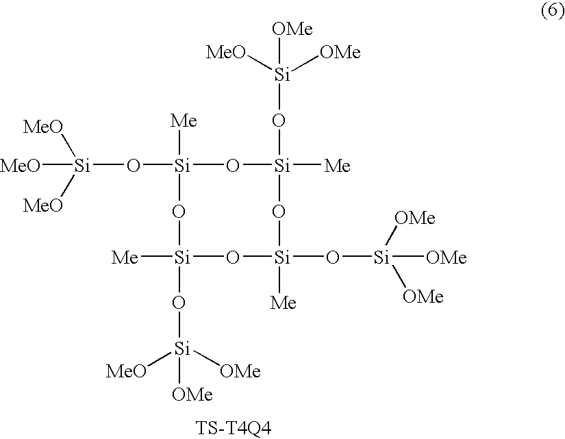
- a preferred cyclic siloxane monomer of Formula 1 is the compound (TS-T4Q4) wherein R 1 is methyl, R 2 is Si(OCH 3 ) 3 and m is 4, represented by Formula 6 below:
- alkoxy silane monomer of Formula 4 examples include methyltriethoxysilane, methyltrimethoxysilane, methyltri-n-propoxysilane, phenyltrimethoxysilane, phenyltriethoxysilane, phenyltrichlorosilane, phenyltrifluorosilane, phenethyltrimethoxysilane, methyltrichlorosilane, methyltribromosilane, methyltrifluorosilane, triethoxysilane, trimethoxysilane, trichlorosilane, trifluorosilane, 3,3,3-trifluoropropyl trimethoxysilane, and cyanoethyltrimethoxysilane.
- the ratio between the monomer of Formula 1 and the monomer of Formula 4 may be in the range of 0.01:99.99 to 99.99:0.01.
- the siloxane polymer used in the present invention preferably has a weight average molecular weight of about 1,000 to 100,000.
- the substituted fullerene used in the present invention functions as a pore per se, and remains in the final film, thereby improving the mechanical strength and thermal conductivity of the film.
- conventional porogens leave pores in a film and are then removed.
- the composition of the present invention is characterized in that the substituted fullerene is used to prepare a uniform solution.
- the substituted fullerene used in the present invention refers to a compound in which an organic group capable of interacting with a solvent is introduced into a fullerene via a double bond reactive with the fullerene. Fullerenes are spherical allotropes of carbon.
- C 60 Sixty-carbon fullerenes (C 60 ) have a diameter of about 7 nm, and ninety-four-carbon fullerenes (C 94 ) have a diameter of about 11 nm. Since these fullerenes take the form of a hollow sphere, they can function as a pore per se. As explained previously, carbon atoms of fullerenes are bonded to each other to form spheres, which makes the fullerenes structurally stable. Further, it is known that covalent bonding between carbon atoms of fullerenes allows the fullerenes to have superior mechanical properties and high chemical and thermal stability.
- the substituted fullerene used in the present invention is a compound in which a reactive organic group capable of interacting with an organic solvent is introduced into a fullerene using a double bond reactive with the fullerene, and thus it has a uniform distribution in a coating solution.
- the reactive organic group can be selected from alkyl, hydroxyl, carboxyl, ether, aldehyde, ketone, ester, amine, amide, and the like.
- One or more reactive organic group can be introduced.
- substituted fullerene examples include fullerenes represented by Formulae 7 and 8 below: wherein the substituents R are each independently a C 1 -C 20 alkyl group or a C 2 -C 30 acyl group, wherein the substituents R are each independently represented by Formula 9 or 10 below:
- the substituent in the substituted fullerene of Formula 7 permits the fullerene molecules to be well dissolved or dispersed in a solvent, leading to uniform distribution of the fullerene in the composition. As a result, the substituted fullerene is uniformly distributed in a film during or after formation of the film, thus uniformly leaving pores in the dielectric film.
- solvents include: aliphatic hydrocarbon solvents, such as hexane and heptane; aromatic hydrocarbon solvents, such as anisole, mesitylene and xylene; ketone-based solvents, such as methyl isobutyl ketone, 1-methyl-2-pyrrolidinone, cyclohexanone and acetone; ether-based solvents, such as tetrahydrofuran and isopropyl ether; acetate-based solvents, such as ethyl acetate, butyl acetate and propylene glycol methyl ether acetate; alcohol-based solvents, such as isopropyl alcohol and butyl alcohol; amide-based solvents, such as dimethylacetamide and dimethylformamide; silicon-based solvents; and mixtures thereof.
- aliphatic hydrocarbon solvents such as hexane and heptane
- aromatic hydrocarbon solvents such as anisole, mesitylene and xylene
- composition of the present invention preferably comprises about 1-70% by weight of the siloxane polymer as a film-forming material, about 0.1-10% by weight of the substituted fullerene and the balance of the solvent, based on the total weight of the composition.
- the siloxane polymer When the siloxane polymer is used in an amount exceeding 70% by weight, the solution is supersaturated and thus spin coating cannot be employed.
- the content of the substituted fullerene is less than about 0.1% by weight, improvement in the effects provided by the substituted fullerene cannot be anticipated. Meanwhile, when the content of the substituted fullerene exceeds about 10% by weight, there may be problems in that the mechanical properties of the final film are deteriorated and the conductivity of the film is increased.
- the present invention also provides a composition for forming a low-dielectric constant film comprising about 1-70% by weight of at least one silane monomer, about 0.1-10% by weight of a substituted fullerene, and the balance of a solvent containing an acid or base catalyst and water.
- the molar ratio of the silane monomer to the catalyst (an acid or a base) used is in the range of about 1:1 ⁇ 10 ⁇ 5 to about 1:10.
- the molar ratio of the silane monomer to the water used is in the range of about 1:1 to about 1:100.
- the kind of the silane monomer used herein is the same as that of the monomer(s) used to prepare the siloxane polymer.
- suitable acid catalysts examples include, without particular limitation, any acid catalyst known in the art.
- the acid catalyst there can be used hydrochloric acid, nitric acid, benzene sulfonic acid, oxalic acid, formic acid, or the like.
- the base catalyst there can be used potassium hydroxide, sodium hydroxide, triethylamine, sodium bicarbonate, pyridine, or the like.
- composition of the present invention may further comprise about 0.1-50% by weight of a porogen, based on the total weight of the solids.
- suitable porogens include any known porogen that can be used to form porous dielectric films, and specific examples thereof include, but are not limited to, polycaprolactone, ⁇ -cyclodextrin, ⁇ -cyclodextrin, and ⁇ -cyclodextrin.
- a surfactant selected from anionic surfactants, cationic surfactants, non-ionic surfactants, and block copolymers.
- anionic surfactants include sulfates, sulfonates, phosphates, and carboxylic acids.
- cationic surfactants include alkylammonium salts, gemini surfactants, cetyltrimethylpiperidinium salts, and dialkyldimethylammonium salts.
- non-ionic surfactants examples include BRij surfactants, primary amines, poly(oxyethylene) oxides, octaethylene glycol monodecyl ether, octaethylene glycol monohexadecyl ether, octylphenoxypolyethoxy (9-10) ethanol (Triton X-1 00), and block copolymers.
- preferred surfactants are polyethylene oxide-propylene oxide block copolymers represented by Formula 13, a polyethylene oxide-propylene oxide-polyethylene oxide triblock copolymers represented by Formula 14, cyclodextrin derivatives represented by Formula 15, cetyltrimethylammonium bromide (CTAB), octylphenoxypolyethoxy (9-10) ethanol (Triton X-100), and ethylenediaminealkoxylate block copolymers.
- CTAB cetyltrimethylammonium bromide
- Triton X-100 Triton X-100
- ethylenediaminealkoxylate block copolymers preferred surfactants.
- R 14 and R 15 are each independently a hydrogen atom, a C 2 -C 30 acyl group, a C 1 -C 20 alkyl group, or a silicon (Si) compound represented by Sir 1 r 2 r 3 (in which r 1 , r 2 and r 3 are each independently a hydrogen atom, a C 1 -C 6 alkyl group, a C 1 -C 6 alkoxy group, or a C 6 -C 20 aryl group); m is an integer from 20 to 80; and n is an integer from 2 to 200.
- R 16 and R 17 are each independently a hydrogen atom, a C 2 -C 30 acyl group, a C 1 -C 20 alkyl group, or a silicon compound represented by Sir 1 r 2 r 3 (in which r 1 , r 2 and r 3 are each independently a hydrogen atom, a C 1 -C 6 alkyl group, a C 1 -C 6 alkoxy group, or a C 6 -C 20 aryl group); I is an integer from 2 to 200; m is an integer from 20 to 80; and n is an integer from 2 to 200.
- R 18 , R 19 and R 20 are each independently a hydrogen atom, a C 2 -C 30 acyl group, a C 1 -C 20 alkyl group, or a silicon compound represented by Sir 1 r 2 r 3 (in which r 1 , r 2 and r 3 are each independently a hydrogen atom, a C 1 -C 6 alkyl group, a C 1 -C 6 alkoxy group, or a C 6 -C 20 aryl group); and q is an integer from 5 to 8.
- the present invention also provides a method for forming a low-dielectric constant film using the composition.
- a low-dielectric constant film is formed by mixing the siloxane polymer, the substituted fullerene alone or in a mixture with another porogen, and the solvent to prepare a coating solution, applying the coating solution coated to a substrate, followed by curing.
- a low-dielectric constant film may be also formed by mixing the silane monomer, the substituted fullerene alone or in a mixture with another porogen, solvent, an acid or base catalyst and water to prepare a coating solution, applying the coating solution coated to a substrate, followed by curing.
- the substrate is not specially limited so long as the objects of the present invention are not impaired.
- suitable substrates include any substrate capable of withstanding heat-curing conditions, for example, glass substrates, silicon wafers, and plastic substrates. These substrates can be properly selected according to intended applications.
- the composition of the present invention can be applied to the substrate by common coating processes, including, but not limited to, spin coating, dip coating, spray coating, flow coating, and screen printing. In view of ease of application and uniformity, spin coating is most preferred coating process.
- spin coating is most preferred coating process.
- the spin speed is preferably adjusted within the range of about 800 to 5,000 rpm.
- the solvent is evaporated to dry the film. The drying can be performed by simply exposing the film to the atmosphere, subjecting the film to a vacuum in the initial stage of the subsequent curing, or thermally curing the film at about 150° C. to 600° C. and preferably at about 200° C. to 450° C. for about 1-180 minutes to form a crack-free insoluble film.
- crack-free film is meant a film having no crack when observed under an optical microscope at a magnification of 1,000 ⁇ .
- insoluble film is meant a film which is substantially insoluble in the solvents used for the deposition of the siloxane polymer to form the film and in any solvent described as being useful for the coating of resins.
- a dielectric film composed of the siloxane polymer alone has a dielectric constant not higher than 3.0 and can be used as a semiconductor dielectric low-dielectric constant coating film.
- the dielectric constant of a dielectric film composed of the siloxane polymer and the porogen can be controlled depending on the contents of the components.
- the dielectric film comprising the siloxane polymer and the substituted fullerene according to the present invention has a low dielectric constant and superior mechanical properties, including toughness, elasticity, etc.
- an improvement in the thermal conductivity of the dielectric film according to the present invention can be anticipated in view of inherent characteristics of the fullerene. Accordingly, the dielectric film of the present invention can be useful as a semiconductor interlayer dielectric film.
- the obtained filtrate was diluted with 200 ml of tetrahydrofuran (THF), and then 177.8 mmol (13.83 g) of triethylamine was added thereto. After the resulting solution was cooled to 0° C., 177.8 mmol (25.0 g) of chlorotrimethoxysilane was slowly added thereto. The resulting mixture was allowed to warm to room temperature. The mixture was reacted for 12 hours. The reaction solution was filtered through celite, and the obtained filtrate was concentrated at a reduced pressure of about 0.1 torr to remove volatile materials, thereby making possible the colorless liquid monomer of Formula 6 below:
- the reaction solution was transferred to a separatory funnel, followed by the addition of diethyl ether in the same amount as that of the initially added tetrahydrofuran along with tetrahydrofuran.
- the resulting mixture was washed three times with water in the amount of one tenth of the total volume of the solvents used, and was then concentrated at reduced pressure to remove volatile materials, giving a polymer in the form of a white powder.
- the polymer was dissolved in tetrahydrofuran until it became transparent, and was filtered through a filter (pore size: 0.2 ⁇ m). Water was slowly added to the filtrate to obtain a precipitate in the form of a white powder. The precipitate was dried at 0 ⁇ 20° C.
- Si—OH, Si—OCH 3 and Si—CH 3 in the polymer were measured to be 33.80%, 1.10%, and 65.10%, respectively.
- the contents (%) of Si—OH, Si—OCH 3 and Si—CH 3 in the siloxane polymer were determined by nuclear magnetic resonance (NMR, Bruker) analysis.
- Si—OH (%) Area (Si—OH) ⁇ [Area (Si—OH)+Area (Si—OCH 3 )/3+Area (Si—CH 3 )/3] ⁇ 100.
- Si—OCH 3 (%) Area (Si—OCH 3 )/3+[Area (Si—OH)+Area (Si—OCH 3 )/3+Area (Si—CH 3 )/3] ⁇ 100.
- Si—CH 3 (%) Area (Si—CH 3 )/3+[Area (Si—OH)+Area (Si—OCH 3 )/3+Area (Si—CH 3 )/3] ⁇ 100.
- siloxane polymer (B) was synthesized in the same manner as in the synthesis of siloxane polymer (A), except that 10 mmol of the polyfunctional siloxane monomer of Formula 6 alone prepared in Preparative Example 1 was used. At this time, 4.055 mmol of HCl and 1351.4 mmol of water were used. As a result, the contents of Si—OH, Si—OCH 3 and Si—CH 3 in the polymer were measured to be 43.5%, 0.6% and 55.9%, respectively.
- 0.611 g of polymer (A) as a siloxane polymer and 6 mg (1 % by weight relative to the polymer) of the hexasubstituted modified fullerene of Formula 8 as an additive were added to propylene glycol methyl ether acetate as a solvent to prepare a coating solution having a solid content of 24 wt %.
- the coating solution was spin-coated on a silicon wafer at 2,000 rpm for 30 seconds, sequentially pre-heated on a hot plate under a nitrogen atmosphere at 150° C. for one minute and at 250° C. for one minute, and dried to form a film.
- the film was heated to 420° C. at a rate of 3° C./min. under vacuum for one hour to form a dielectric film A-1.
- Dielectric films A-2, A-3 and A-4 were formed in the same manner as above, except that 12 mg (2% by weight relative to the polymer), 31 mg (5% by weight relative to the polymer) and 61 mg (10% by weight relative to the polymer) of the hexasubstituted modified fullerene of Formula 8 were used, respectively.
- the thickness, refractive index, dielectric constant, hardness, elastic modulus and carbon content of the dielectric films were measured. The results are shown in Table 1.
- a thermal silicon oxide film was coated to a thickness of 3,000 ⁇ on a boron-doped p-type silicon wafer, and then a 100 ⁇ -thick titanium film, a 2,000 ⁇ -thick aluminum film and a 100 ⁇ -thick film were sequentially deposited on the silicon oxide film using a metal evaporator.
- a dielectric film was formed on the resulting structure, after which a 100 ⁇ -thick circular titanium thin film (diameter: 1 mm) and a 5,000 ⁇ -thick aluminum thin film (diameter: 1 mm) were sequentially deposited on the dielectric film using a hardmask designed so as to have an electrode diameter of 1 mm, to form a low-dielectric constant film having a MIM (metal-insulator-metal) structure.
- MIM metal-insulator-metal
- the capacitance of the thin film was measured around 10 kHz, 100 kHz and 1 MHz using a PRECISION LCR METER (HP4284A) accompanied with a probe station (Micromanipulatior 6200 probe station), and the thickness of the thin film was measured using a prism coupler.
- the thickness and refractive index of the thin films were measured using an elipsometor and a prism coupler, respectively.
- the hardness and elastic modulus of the dielectric thin films were determined by quantitative analysis using a Nanoindenter II (MTS). Specifically, after the nanoindenter was indented into the thin films until the indentation depth reached 10% of its overall thickness, the hardness and modulus of the thin films were measured. The thickness of the thin films was measured using a prism coupler. To ensure better reliability of the measurement in the following examples and comparative examples, the hardness and modulus were measured at a total of 6 indention points on the dielectric films, and the obtained values were averaged.
- MTS Nanoindenter II
- Dielectric constant films B-1 to B-4 were formed in the same manner as in the formation of dielectric films A-1 to A-4, except that the weight of polymer (A) was changed from 0.611 g to 0.550 g, and 0.061 g of heptakis(2,3,6-tri-O-methyl)- ⁇ -cyclodextrin (tCD) was added as another porogen. At this time, the weights of the modified fullerene used to form dielectric constant films B-1 to B-4 were the same as those of the modified fullerene used to form dielectric constant films A-1 to A-4, respectively. The thickness, refractive index, dielectric constant, hardness, elastic modulus and carbon content of the dielectric films were measured. The results are shown in Table 1.
- Dielectric constant films C-1 to C-4 were formed in the same manner as in the formation of dielectric films A-1 to A-4, except that the weight of polymer (A) was changed from 0.611 g to 0.489 g, and 0.122 g of heptakis(2,3,6-tri-O-methyl)- ⁇ -cyclodextrin (tCD) was added as another porogen. At this time, the weights of the modified fullerene used to form dielectric constant films C-1 to C-4 were the same as those of the modified fullerene used to form dielectric constant films A-1 to A-4, respectively. The thickness, refractive index, dielectric constant, hardness, elastic modulus and carbon content of the dielectric films were measured. The results are shown in Table 1.
- Dielectric constant films D-1 to D-4 were formed in the same manner as in the formation of dielectric films A-1 to A-4, except that polymer (B) was used instead of polymer (A).
- the thickness, refractive index, dielectric constant, hardness, elastic modulus and carbon content of the dielectric films were measured. The results are shown in Table 1.
- Dielectric constant films A to D were formed in the same manner as in the formation of dielectric films A-1 to A-4, except that no substituted fullerene was added. The thickness, refractive index, dielectric constant, hardness, elastic modulus and carbon content of the dielectric films were measured. The results are shown in Table 1. TABLE 1 Physical Properties Dielectric Refractive constant Elastic Thickness Example No.
- the dielectric films formed in the examples using the compositions of the present invention have a low dielectric constant despite a small thickness, compared to the dielectric films comprising no substituted fullerene formed in the comparative examples. Accordingly, the substituted fullerene can function as a porogen to form pores in the films.
- the substituted fullerene included in the composition for forming a low-dielectric constant film according to the present invention is highly soluble in a solvent, a uniform solution can be prepared despite the addition of a large amount of the fullerene.
- the substituted fullerene advantageously lowers the dielectric constant of a thin film and improves the mechanical properties, such as hardness and elastic modulus, of the thin film.
- the substituted fullerene used in the present invention contributes to the reduction in dielectric constant and the improvement in mechanical properties despite the addition of an extremely small amount of the fullerene.
- an improvement in thermal conductivity can be anticipated in view of inherent characteristics of the fullerene.
Abstract
Description
- This non-provisional application claims the benefit of priority under 35 U.S.C. § 119(a) of Korean Patent Application No. 2005-11405 filed on Feb. 7, 2005, which is herein incorporated by reference.
- 1. Field of the Disclosure
- The present disclosure relates to a composition for forming a low-dielectric constant film, a low-dielectric constant film formed from the composition, and a method for forming the low-dielectric constant film. More particularly, the present disclosure relates to a composition for forming a low-dielectric constant film comprising a substituted fullerene wherein the composition can be used to form a low-dielectric constant film having superior mechanical properties and thermal conductivity, a low-dielectric constant film formed from the composition, and a method for forming the low-dielectric constant film.
- 2. Description of the Related Art
- With recent advances in semiconductor manufacturing technology, semiconductor devices have become smaller in size and more densely integrated. Such trends are likely to continue. The degree of integration of devices in the fields of semiconductors refers to the number of constituent devices formed in a single semiconductor chip and indicates how many logic devices (which are fabricated by integrating multifunctional devices, e.g., diodes, resistors and transistors) are included in one chip. That is, the higher the degree of integration, the better the performance. However, as devices are more highly integrated, various factors, such as metal interconnections, may affect the performance of the devices. In addition, interlayer dielectric films having a low charge capacity are required in order to lower the resistance and capacity in interconnections. For this purpose, attempts have been made to use low-dielectric constant materials for interlayer dielectric films. For instance, U.S. Pat. Nos. 3,615,272, 4,399,266 and 4,999,397 disclose polysilsesquioxanes having a dielectric constant of about 2.5˜3.1 which can be applied by spin-on deposition (“SOD”), which can replace SiO2 having a dielectric constant of around 4.00 applied by a conventional chemical vapor deposition (CVD) technique. Further, U.S. Pat. No. 5,965,679 teaches polyphenylenes as organic polymers having a dielectric constant between about 2.65 and about 2.70. However, this dielectric constant range is not sufficiently low to satisfy an increasing demand to fabricate high-speed devices requiring an ultra-low dielectric constant not higher than 2.50. For this reason, there have been a number of trials to incorporate air having a dielectric constant of 1.0 into the organic or inorganic film-forming materials.
- U.S. Pat. No. 6,231,989 discloses a method forming a porous thin film by mixing hydrogen silsesquioxane with a high boiling point solvent capable of forming pores, and treating the mixture with ammonia. Methods for forming an insulator with an ultra-low dielectric constant are found in U.S. Pat. Nos. 6,093,636 and 6,107,357. According to these methods, the above-mentioned organic or inorganic film-forming material is mixed with a predetermined amount of a thermally decomposable porogen during film formation to form a thin film, and then the porogen is decomposed at high temperatures to form pores. U.S. Pat. Nos. 6,204,202, 6,413,882, 6,423,770 and 6,406,794 describe methods for producing a low-dielectric constant porous thin film utilizing a polyalkyleneoxide amphoteric surfactant as a porogen. According to these methods, however, pores formed in the porous thin film are partially or completely interconnected, leading to deterioration in the physical properties of the dielectric film, and chemicals used as materials of low-dielectric constant interlayer dielectric films for semiconductor devices and metal atoms are diffused into the pores. Accordingly, it is important to make the size of pores smaller and the interconnectivity of pores lower.
- Fullerenes, which are sometimes called “bucky balls”, whose molecular structure resembles a soccer ball are the most recently discovered materials consisting of sixty carbon atoms (C60). Bucky ball was named for Buckminster Fuller, the architect who designed the geodesic dome, because it has a similar shape to that of the dome. Fullerenes are entirely novel compounds which were discovered and isolated from sooty residue remaining after a piece of graphite was irradiated with laser beams by a group of researchers. Fullerene molecules can trap very tiny materials therein, like bird cages, and are very rigid and slippery. Further, fullerene molecules can open so that other materials can be captured and inserted therein, and can be linked in the form of a tube. Moreover, fullerenes can transmit information from computer chips via atomic-scale lines, can transport drugs necessary for the body, and can be used to produce hard and sharp cutting tools and very rigid plastics. Since fullerenes are expected to be increasingly used in various applications, scientists around the world have paid considerable attention to many potential applications for fullerenes.
- On the other hand, there have been a number of suggestions regarding the formation of low-dielectric constant films in which air is incorporated using fullerenes as porogens. For example, U.S. Pat. No. 5,744,399 describes a process for lowering the dielectric constant of a layer on a semiconductor wafer by introducing a fullerene into a matrix-forming material. This process comprises the steps of forming on the wafer a composite layer comprising a matrix-forming material and a fullerene, and removing the fullerene from the composite layer to leave an open porous structure wherein the fullerene is removed by contacting the composite layer with a liquid capable of dissolving the fullerene or by oxidizing the fullerene. U.S. Pat. No. 6,287,979 describes the formation of a porous air bridge layer comprising a fullerene (buckminsterfullerene) wherein the fullerene reacts with an oxygen plasma and is removed. The former two U.S. patent publications are associated with a decrease in dielectric constant utilizing the low dielectric constant of air by incorporating a fullerene in a matrix-forming material or a layer and removing the fullerene in the subsequent step to leave pores in situ. At this time, the fullerene functions only as a porogen and does not remain in a final device. Accordingly, the mechanical strength and thermal conductivity of dielectric films for the final device are inevitably deteriorated.
- In recent years, U.S. Patent Publication No. 2004/0121501 A1 mentions the introduction of a fullerene inside an interconnect insulator by using plasma-enhanced chemical vapor deposition, or possibly spin-on deposition (SOD). However, since the use of the fullerene in SOD requires dissolution of the fullerene in a solution phase, the problem arises in that since the fullerene in a solid state is not dissolved, a dispersant or an additional operation must be employed to prepare an emulsion of the fullerene. Such an emulsion limits the amount of the fullerene to be added and inevitably results in the deterioration in the roughness of the thin film.
- Therefore, the present invention has been made in view of the above problems, and it is an object of the present invention to provide a composition for forming a low-dielectric constant film comprising a substituted fullerene wherein the composition can be used to form a low-dielectric constant film having superior mechanical strength and thermal conductivity.
- It is another object of the present invention to provide a method for forming a low-dielectric constant film with superior mechanical strength using a fullerene by a simplified procedure at a reduced cost.
- In accordance with one aspect of the present invention for achieving the above objects, there is provided a composition for forming a low-dielectric constant film which comprises a siloxane polymer, a substituted fullerene, and a solvent.
- In accordance with another aspect of the present invention, there is provided a composition for forming a low-dielectric constant film which comprises at least one silane monomer, a substituted fullerene, and a solvent containing an acid or base catalyst and water.
- In accordance with yet another aspect of the present invention, there is provided a method for forming a low-dielectric constant film by coating the composition comprising a substituted fullerene on a substrate, followed by curing.
- The present inventors have earnestly and intensively conducted research to produce a low-dielectric constant film by forming pores in a material for forming the film (i.e. a film-forming material), and at the same time, to improve the mechanical properties and thermal conductivity of the film during and after formation of the film. As a result, the present inventors have found that the addition of a fullerene to the film-forming material was effective in the formation of a low-dielectric constant film, but the fullerene was not dissolved in a solution phase. The present inventors have made efforts to solve problems arising from the insolubility of the fullerene, and as a result, unexpectedly found that the addition of a substituted fullerene having an organic group to the film-forming material leads to the preparation of a uniform solution. By taking advantage of these findings, the dielectric constant of the film could be lowered and the mechanical properties and thermal conductivity of the film could be improved by including the substituted fullerene in the film without the removal of the substituted fullerene during or after formation of the film, thus accomplishing the present invention.
- Hereinafter, preferred embodiments of the present invention will be described in greater detail.
- The present invention provides a composition for forming a low-dielectric constant film comprising about 1-70% by weight of a siloxane polymer as a film-forming material, about 0.1-10% by weight of a substituted fullerene, and the balance of a solvent. A low-dielectric constant film having superior mechanical strength can be formed by applying the composition to a substrate, followed by curing. The low-dielectric constant film thus formed can be applied as a low-dielectric semiconductor interlayer dielectric film and can be used in a wide variety of applications, including display materials, chemical sensors, biocatalysts, insulators, packaging materials, etc.
- Siloxane polymers that can be used in the present invention are not specially restricted so long as they have the structure Si—O—C.
- For example, the siloxane polymer used in the present invention may be a siloxane homopolymer prepared by hydrolysis and polycondensation of one monomer selected from the group consisting of a polyfunctional cyclic siloxane monomer represented by Formula 1 below:

wherein R1 is a hydrogen atom, a C1-C3 alkyl group, or a C6-C15 aryl group; and R2 is a hydrogen atom, a C1-C10 alkyl group, or SiX1X2X3 (in which X1, X2 and X3 are each independently a hydrogen atom, a C1-C3 alkyl group, a C1-C10 alkoxy group, or a halogen atom); and m is an integer from 3 to 8, -
- a siloxane monomer having an organic bridge represented by Formula 2 or 3 below:

wherein R is a hydrogen atom, a C1-C3 alkyl group, or a C6-C15 aryl group; X1, X2 and X3 are each independently a hydrogen atom, a C1-C3 alkyl, a C1-C10 alkoxy, or a halogen atom, with the proviso that at least one of X1, X2 and X3 is a hydrolysable functional group; m is an integer from 0 to 10; and n is an integer from 3 to 8,
X3X2X1Si—M—SiX1X2X3 (3)
wherein X1, X2 and X3 are each independently a hydrogen atom, a C1-3 alkyl group, a C1-C10 alkoxy group, or a halogen atom, with the proviso that at least one of X1, X2 and X3 is a hydrolysable functional group; and M is a single bond, a C1-10 alkylene group, or a C6-15 arylene group, and - a linear alkoxy silane monomer represented by Formula 4 or 5 below:
(R1)nSi(OR2)4−n (4)
wherein R1 is a hydrogen atom, a C1-3 alkyl group, a halogen atom, or a C6-15 aryl group; R2 is a hydrogen atom, a C1-3 alkyl group, or a C6-15 aryl group, with the proviso that at least one of R1 and OR2 is a hydrolysable functional group; and n is an integer from 0 to 3,
wherein the substituents R1 are each independently a hydrogen atom, a C1-3 alkyl group, a C1-10 alkoxy group, a hydroxyl group, or a halogen atom, with the proviso that at least one of the substituents R1 is a hydrolysable functional group; and n is an integer from 0 to 30, in an organic solvent in the presence of water and an acid or base catalyst.
- a siloxane monomer having an organic bridge represented by Formula 2 or 3 below:
- The siloxane polymer used in the present invention may be a siloxane copolymer prepared by hydrolysis and polycondensation of at least two monomers selected from the monomers of Formulae 1 to 5 in an organic solvent in the presence of water and an acid or base catalyst.
- A preferred cyclic siloxane monomer of Formula 1 is the compound (TS-T4Q4) wherein R1 is methyl, R2 is Si(OCH3)3 and m is 4, represented by Formula 6 below:
- Specific examples of the alkoxy silane monomer of Formula 4 include methyltriethoxysilane, methyltrimethoxysilane, methyltri-n-propoxysilane, phenyltrimethoxysilane, phenyltriethoxysilane, phenyltrichlorosilane, phenyltrifluorosilane, phenethyltrimethoxysilane, methyltrichlorosilane, methyltribromosilane, methyltrifluorosilane, triethoxysilane, trimethoxysilane, trichlorosilane, trifluorosilane, 3,3,3-trifluoropropyl trimethoxysilane, and cyanoethyltrimethoxysilane.
- Specific examples of siloxane polymers that can be used in the present invention include homopolymers of the cyclic siloxane monomer of Formula 1, and copolymers of the cyclic siloxane monomer of Formula 1 and the cyclic alkoxy silane monomer of Formula 4. In the case of the copolymers, the ratio between the monomer of Formula 1 and the monomer of Formula 4 may be in the range of 0.01:99.99 to 99.99:0.01.
- The siloxane polymer used in the present invention preferably has a weight average molecular weight of about 1,000 to 100,000.
- The substituted fullerene used in the present invention functions as a pore per se, and remains in the final film, thereby improving the mechanical strength and thermal conductivity of the film. In contrast, conventional porogens leave pores in a film and are then removed. Particularly, the composition of the present invention is characterized in that the substituted fullerene is used to prepare a uniform solution. The substituted fullerene used in the present invention refers to a compound in which an organic group capable of interacting with a solvent is introduced into a fullerene via a double bond reactive with the fullerene. Fullerenes are spherical allotropes of carbon. Sixty-carbon fullerenes (C60) have a diameter of about 7 nm, and ninety-four-carbon fullerenes (C94) have a diameter of about 11 nm. Since these fullerenes take the form of a hollow sphere, they can function as a pore per se. As explained previously, carbon atoms of fullerenes are bonded to each other to form spheres, which makes the fullerenes structurally stable. Further, it is known that covalent bonding between carbon atoms of fullerenes allows the fullerenes to have superior mechanical properties and high chemical and thermal stability.
- Particularly, the substituted fullerene used in the present invention is a compound in which a reactive organic group capable of interacting with an organic solvent is introduced into a fullerene using a double bond reactive with the fullerene, and thus it has a uniform distribution in a coating solution. The reactive organic group can be selected from alkyl, hydroxyl, carboxyl, ether, aldehyde, ketone, ester, amine, amide, and the like. One or more reactive organic group can be introduced.
- Specific examples of the substituted fullerene include fullerenes represented by Formulae 7 and 8 below:

wherein the substituents R are each independently a C1-C20 alkyl group or a C2-C30 acyl group,
wherein the substituents R are each independently represented by Formula 9 or 10 below:
- The substituent in the substituted fullerene of Formula 7 permits the fullerene molecules to be well dissolved or dispersed in a solvent, leading to uniform distribution of the fullerene in the composition. As a result, the substituted fullerene is uniformly distributed in a film during or after formation of the film, thus uniformly leaving pores in the dielectric film.
- As the substituted fullerene, there may also be used [6,6]-phenyl-C61 butyric acid methyl ester (F[5,6]) of Formulae 11 and methanofullerene (1 -(3-methoxycarbonyl) propyl-1-phenyl[6,6] C61 (M [6,6]) of Formulae 12 below:

- Methods for synthesizing the fullerenes of Formulae 7 and 8 are already described and known in the literature (see, Camps, X; Hirsch, A. J. Chem. Soc. Perkin trans. 1, 11, 1595 (1997)).
- There is no particular restriction on the type of the solvent used in the present invention, and examples of preferred solvents include: aliphatic hydrocarbon solvents, such as hexane and heptane; aromatic hydrocarbon solvents, such as anisole, mesitylene and xylene; ketone-based solvents, such as methyl isobutyl ketone, 1-methyl-2-pyrrolidinone, cyclohexanone and acetone; ether-based solvents, such as tetrahydrofuran and isopropyl ether; acetate-based solvents, such as ethyl acetate, butyl acetate and propylene glycol methyl ether acetate; alcohol-based solvents, such as isopropyl alcohol and butyl alcohol; amide-based solvents, such as dimethylacetamide and dimethylformamide; silicon-based solvents; and mixtures thereof.
- The solids content of the composition according to the present invention is not specially restricted. As described above, the composition of the present invention preferably comprises about 1-70% by weight of the siloxane polymer as a film-forming material, about 0.1-10% by weight of the substituted fullerene and the balance of the solvent, based on the total weight of the composition.
- When the siloxane polymer is used in an amount exceeding 70% by weight, the solution is supersaturated and thus spin coating cannot be employed. When the content of the substituted fullerene is less than about 0.1% by weight, improvement in the effects provided by the substituted fullerene cannot be anticipated. Meanwhile, when the content of the substituted fullerene exceeds about 10% by weight, there may be problems in that the mechanical properties of the final film are deteriorated and the conductivity of the film is increased.
- The present invention also provides a composition for forming a low-dielectric constant film comprising about 1-70% by weight of at least one silane monomer, about 0.1-10% by weight of a substituted fullerene, and the balance of a solvent containing an acid or base catalyst and water. The molar ratio of the silane monomer to the catalyst (an acid or a base) used is in the range of about 1:1×10⁻⁵ to about 1:10. On the other hand, the molar ratio of the silane monomer to the water used is in the range of about 1:1 to about 1:100.
- The kind of the silane monomer used herein is the same as that of the monomer(s) used to prepare the siloxane polymer.
- On the other hand, examples of suitable acid catalysts that can be used in the present invention include, without particular limitation, any acid catalyst known in the art. As the acid catalyst, there can be used hydrochloric acid, nitric acid, benzene sulfonic acid, oxalic acid, formic acid, or the like. As the base catalyst, there can be used potassium hydroxide, sodium hydroxide, triethylamine, sodium bicarbonate, pyridine, or the like.
- The composition of the present invention may further comprise about 0.1-50% by weight of a porogen, based on the total weight of the solids.
- Examples of suitable porogens that can be used in the present invention include any known porogen that can be used to form porous dielectric films, and specific examples thereof include, but are not limited to, polycaprolactone, α-cyclodextrin, β-cyclodextrin, and γ-cyclodextrin.
- As the porogen, there can be used a surfactant selected from anionic surfactants, cationic surfactants, non-ionic surfactants, and block copolymers. Examples of anionic surfactants include sulfates, sulfonates, phosphates, and carboxylic acids. Examples of cationic surfactants include alkylammonium salts, gemini surfactants, cetyltrimethylpiperidinium salts, and dialkyldimethylammonium salts. Examples of non-ionic surfactants include BRij surfactants, primary amines, poly(oxyethylene) oxides, octaethylene glycol monodecyl ether, octaethylene glycol monohexadecyl ether, octylphenoxypolyethoxy (9-10) ethanol (Triton X-1 00), and block copolymers. Of these, preferred surfactants are polyethylene oxide-propylene oxide block copolymers represented by Formula 13, a polyethylene oxide-propylene oxide-polyethylene oxide triblock copolymers represented by Formula 14, cyclodextrin derivatives represented by Formula 15, cetyltrimethylammonium bromide (CTAB), octylphenoxypolyethoxy (9-10) ethanol (Triton X-100), and ethylenediaminealkoxylate block copolymers.

wherein R14 and R15 are each independently a hydrogen atom, a C2-C30 acyl group, a C1-C20 alkyl group, or a silicon (Si) compound represented by Sir1r2r3 (in which r1, r2 and r3 are each independently a hydrogen atom, a C1-C6 alkyl group, a C1-C6 alkoxy group, or a C6-C20 aryl group); m is an integer from 20 to 80; and n is an integer from 2 to 200.
wherein R16 and R17 are each independently a hydrogen atom, a C2-C30 acyl group, a C1-C20 alkyl group, or a silicon compound represented by Sir1r2r3 (in which r1, r2 and r3 are each independently a hydrogen atom, a C1-C6 alkyl group, a C1-C6 alkoxy group, or a C6-C20 aryl group); I is an integer from 2 to 200; m is an integer from 20 to 80; and n is an integer from 2 to 200.
wherein R18, R19 and R20 are each independently a hydrogen atom, a C2-C30 acyl group, a C1-C20 alkyl group, or a silicon compound represented by Sir1r2r3 (in which r1, r2 and r3 are each independently a hydrogen atom, a C1-C6 alkyl group, a C1-C6 alkoxy group, or a C6-C20 aryl group); and q is an integer from 5 to 8. - The present invention also provides a method for forming a low-dielectric constant film using the composition. According to the method of the present invention, a low-dielectric constant film is formed by mixing the siloxane polymer, the substituted fullerene alone or in a mixture with another porogen, and the solvent to prepare a coating solution, applying the coating solution coated to a substrate, followed by curing.
- According to the method of the present invention, a low-dielectric constant film may be also formed by mixing the silane monomer, the substituted fullerene alone or in a mixture with another porogen, solvent, an acid or base catalyst and water to prepare a coating solution, applying the coating solution coated to a substrate, followed by curing.
- The substrate is not specially limited so long as the objects of the present invention are not impaired. Examples of suitable substrates include any substrate capable of withstanding heat-curing conditions, for example, glass substrates, silicon wafers, and plastic substrates. These substrates can be properly selected according to intended applications.
- The composition of the present invention can be applied to the substrate by common coating processes, including, but not limited to, spin coating, dip coating, spray coating, flow coating, and screen printing. In view of ease of application and uniformity, spin coating is most preferred coating process. Upon spin coating, the spin speed is preferably adjusted within the range of about 800 to 5,000 rpm. After the coating, if required, the solvent is evaporated to dry the film. The drying can be performed by simply exposing the film to the atmosphere, subjecting the film to a vacuum in the initial stage of the subsequent curing, or thermally curing the film at about 150° C. to 600° C. and preferably at about 200° C. to 450° C. for about 1-180 minutes to form a crack-free insoluble film. As used herein, by “crack-free film” is meant a film having no crack when observed under an optical microscope at a magnification of 1,000×. As used herein, by “insoluble film” is meant a film which is substantially insoluble in the solvents used for the deposition of the siloxane polymer to form the film and in any solvent described as being useful for the coating of resins. When the coating solution contains a porogen, the heat-curing temperature is properly determined taking the decomposition temperature of the porogen into consideration.
- A dielectric film composed of the siloxane polymer alone has a dielectric constant not higher than 3.0 and can be used as a semiconductor dielectric low-dielectric constant coating film. The dielectric constant of a dielectric film composed of the siloxane polymer and the porogen can be controlled depending on the contents of the components. The dielectric film comprising the siloxane polymer and the substituted fullerene according to the present invention has a low dielectric constant and superior mechanical properties, including toughness, elasticity, etc. In addition, an improvement in the thermal conductivity of the dielectric film according to the present invention can be anticipated in view of inherent characteristics of the fullerene. Accordingly, the dielectric film of the present invention can be useful as a semiconductor interlayer dielectric film.
- Preferred embodiments of the present invention will now be described in detail with reference to the following examples. However, these examples are given for the purpose of illustration and are not to be construed as limiting the scope of the invention.
- 41.6 mmol (10.00 g) of 2,4,6,8-tetramethyl-2,4,6,8-cyclotetrasiloxane was diluted with 100 ml of tetrahydrofuran in a flask, and then 700 mg of 10 wt % palladium/charcoal (Pd/C) was added thereto. Subsequently, 177.8 mmol (3.20 ml) of distilled water was added to the mixture to evolve hydrogen gas. After the hydrogen gas was removed, the reaction was allowed to proceed at room temperature for 5 hours. The reaction solution was filtered through celite and MgSO4. The obtained filtrate was diluted with 200 ml of tetrahydrofuran (THF), and then 177.8 mmol (13.83 g) of triethylamine was added thereto. After the resulting solution was cooled to 0° C., 177.8 mmol (25.0 g) of chlorotrimethoxysilane was slowly added thereto. The resulting mixture was allowed to warm to room temperature. The mixture was reacted for 12 hours. The reaction solution was filtered through celite, and the obtained filtrate was concentrated at a reduced pressure of about 0.1 torr to remove volatile materials, thereby making possible the colorless liquid monomer of Formula 6 below:

- The analytical results of the 1H-NMR spectrum (300 MHz) of the monomer are as follows: δ 0.092 (s, 12H, 4×[—CH3]), 3.58 (s, 36H, 4×[—OCH3]).
- After 65.09 mmol of the polyfunctional siloxane monomer prepared in Preparative Example 1 and 20.36 mmol of methyltrimethoxysilane (MTMS) were placed in a flask, the mixture was diluted with tetrahydrofuran until the concentration of the solution was 0.05 to 0.07M. The reaction solution was cooled to −78° C. 1.222 mmol of hydrochloric acid and 407.2 mmol of water were added to the flask. The reaction temperature was gradually increased to 70° C. At this temperature, the reaction was continued for 16 hours. The reaction solution was transferred to a separatory funnel, followed by the addition of diethyl ether in the same amount as that of the initially added tetrahydrofuran along with tetrahydrofuran. The resulting mixture was washed three times with water in the amount of one tenth of the total volume of the solvents used, and was then concentrated at reduced pressure to remove volatile materials, giving a polymer in the form of a white powder. The polymer was dissolved in tetrahydrofuran until it became transparent, and was filtered through a filter (pore size: 0.2 μm). Water was slowly added to the filtrate to obtain a precipitate in the form of a white powder. The precipitate was dried at 0˜20° C. and 0.1 torr for 10 hours to provide 4.0 g of a siloxane polymer. The contents of Si—OH, Si—OCH3 and Si—CH3 in the polymer were measured to be 33.80%, 1.10%, and 65.10%, respectively. The contents (%) of Si—OH, Si—OCH3 and Si—CH3 in the siloxane polymer were determined by nuclear magnetic resonance (NMR, Bruker) analysis.
- Si—OH (%)=Area (Si—OH)×[Area (Si—OH)+Area (Si—OCH3)/3+Area (Si—CH3)/3]×100.
- Si—OCH3 (%)=Area (Si—OCH3)/3+[Area (Si—OH)+Area (Si—OCH3)/3+Area (Si—CH3)/3]×100.
- Si—CH3 (%)=Area (Si—CH3)/3+[Area (Si—OH)+Area (Si—OCH3)/3+Area (Si—CH3)/3]×100.
- 2.30 g of siloxane polymer (B) was synthesized in the same manner as in the synthesis of siloxane polymer (A), except that 10 mmol of the polyfunctional siloxane monomer of Formula 6 alone prepared in Preparative Example 1 was used. At this time, 4.055 mmol of HCl and 1351.4 mmol of water were used. As a result, the contents of Si—OH, Si—OCH3 and Si—CH3 in the polymer were measured to be 43.5%, 0.6% and 55.9%, respectively.
- 32 μl (0.415 mmol) of 1,8-diazabicyclo[5,4,0]undecene-7 (DBU) was added to a mixture of 100 mg of C60 (0.139 mmol), 69 mg (0.208 mmol) of CBr4 and 0.208 mmol of malonate. After 6 hours of the addition, the reaction mixture was purified by chromatography, providing the first modified fullerene of Formula 7. The second modified fullerene of Formula 8 was prepared by the following procedure. First, a mixture of 100 mg of C60 (0.139 mmol) and 0.286 g (1.39 mmol) of dimethyl amine (DMA) was stirred in 60 ml of toluene at room temperature for 2 hours. 0.460 g (1.39 mmol) of CBr4 and 10 equivalents of malonate were added to the mixture, and then 0.414 ml (2.78 mmol) of 1,8-diazabicyclo[5,4,0]undecene-7 (DBU) was added dropwise thereto. The obtained mixture was purified by chromatography, giving the desired fullerene.
- 0.611 g of polymer (A) as a siloxane polymer and 6 mg (1 % by weight relative to the polymer) of the hexasubstituted modified fullerene of Formula 8 as an additive were added to propylene glycol methyl ether acetate as a solvent to prepare a coating solution having a solid content of 24 wt %. The coating solution was spin-coated on a silicon wafer at 2,000 rpm for 30 seconds, sequentially pre-heated on a hot plate under a nitrogen atmosphere at 150° C. for one minute and at 250° C. for one minute, and dried to form a film. The film was heated to 420° C. at a rate of 3° C./min. under vacuum for one hour to form a dielectric film A-1.
- Dielectric films A-2, A-3 and A-4 were formed in the same manner as above, except that 12 mg (2% by weight relative to the polymer), 31 mg (5% by weight relative to the polymer) and 61 mg (10% by weight relative to the polymer) of the hexasubstituted modified fullerene of Formula 8 were used, respectively.
- The thickness, refractive index, dielectric constant, hardness, elastic modulus and carbon content of the dielectric films were measured. The results are shown in Table 1.
- First, the physical properties of the dielectric films were evaluated in the following procedures.
- 1) Measurement of Dielectric Constant
- First, a thermal silicon oxide film was coated to a thickness of 3,000 Å on a boron-doped p-type silicon wafer, and then a 100 Å-thick titanium film, a 2,000 Å-thick aluminum film and a 100 Å-thick film were sequentially deposited on the silicon oxide film using a metal evaporator. Thereafter, a dielectric film was formed on the resulting structure, after which a 100 Å-thick circular titanium thin film (diameter: 1 mm) and a 5,000 Å-thick aluminum thin film (diameter: 1 mm) were sequentially deposited on the dielectric film using a hardmask designed so as to have an electrode diameter of 1 mm, to form a low-dielectric constant film having a MIM (metal-insulator-metal) structure. The dielectric constant of the low-dielectric constant film was measured. The capacitance of the thin film was measured around 10 kHz, 100 kHz and 1 MHz using a PRECISION LCR METER (HP4284A) accompanied with a probe station (Micromanipulatior 6200 probe station), and the thickness of the thin film was measured using a prism coupler. The dielectric constant of the thin film was calculated according to the following equation:
k=C×d/ε o ×A
in which k is the relative permittivity, C is the capacitance, εo is the dielectric constant of a vacuum (8.8542×10⁻¹² Fm−1), d is the thickness of the dielectric film, and A is the contact cross-sectional area of the electrode. - 2) Thickness And Refractive Index
- The thickness and refractive index of the thin films were measured using an elipsometor and a prism coupler, respectively.
- 3) Hardness And Elastic Modulus
- The hardness and elastic modulus of the dielectric thin films were determined by quantitative analysis using a Nanoindenter II (MTS). Specifically, after the nanoindenter was indented into the thin films until the indentation depth reached 10% of its overall thickness, the hardness and modulus of the thin films were measured. The thickness of the thin films was measured using a prism coupler. To ensure better reliability of the measurement in the following examples and comparative examples, the hardness and modulus were measured at a total of 6 indention points on the dielectric films, and the obtained values were averaged.
- Dielectric constant films B-1 to B-4 were formed in the same manner as in the formation of dielectric films A-1 to A-4, except that the weight of polymer (A) was changed from 0.611 g to 0.550 g, and 0.061 g of heptakis(2,3,6-tri-O-methyl)-β-cyclodextrin (tCD) was added as another porogen. At this time, the weights of the modified fullerene used to form dielectric constant films B-1 to B-4 were the same as those of the modified fullerene used to form dielectric constant films A-1 to A-4, respectively. The thickness, refractive index, dielectric constant, hardness, elastic modulus and carbon content of the dielectric films were measured. The results are shown in Table 1.
- Dielectric constant films C-1 to C-4 were formed in the same manner as in the formation of dielectric films A-1 to A-4, except that the weight of polymer (A) was changed from 0.611 g to 0.489 g, and 0.122 g of heptakis(2,3,6-tri-O-methyl)-β-cyclodextrin (tCD) was added as another porogen. At this time, the weights of the modified fullerene used to form dielectric constant films C-1 to C-4 were the same as those of the modified fullerene used to form dielectric constant films A-1 to A-4, respectively. The thickness, refractive index, dielectric constant, hardness, elastic modulus and carbon content of the dielectric films were measured. The results are shown in Table 1.
- Dielectric constant films D-1 to D-4 were formed in the same manner as in the formation of dielectric films A-1 to A-4, except that polymer (B) was used instead of polymer (A). The thickness, refractive index, dielectric constant, hardness, elastic modulus and carbon content of the dielectric films were measured. The results are shown in Table 1.
- Dielectric constant films A to D were formed in the same manner as in the formation of dielectric films A-1 to A-4, except that no substituted fullerene was added. The thickness, refractive index, dielectric constant, hardness, elastic modulus and carbon content of the dielectric films were measured. The results are shown in Table 1.
TABLE 1 Physical Properties Dielectric Refractive constant Elastic Thickness Example No. index (RI) (k) Hardness Modulus (Å) Comparative 1.379 2.83 1.35 9.23 4,712 Example A Example A-1 1.384 2.76 1.47 9.07 4,836 Example A-2 1.388 2.83 1.48 9.36 5,018 Example A-3 1.400 2.87 1.42 9.08 5,759 Example A-4 1.418 2.81 1.11 7.48 5,997 Comparative 1.338 2.64 1.16 8.00 4,789 Example B Example B-1 1.341 2.45 1.25 8.35 5,165 Example B-2 1.348 2.64 1.23 7.93 5,571 Example B-3 1.351 2.56 1.10 7.34 5,672 Example B-4 1.367 2.67 0.98 6.41 5,976 Comparative 1.307 2.06 0.50 3.75 4,395 Example C Example C-1 1.298 2.04 0.52 3.83 4,574 Example C-2 1.300 1.99 0.54 3.96 4,672 Example C-3 1.311 1.97 0.53 4.15 5,064 Example C-4 1.338 2.07 0.52 4.15 5,571 Comparative 1.395 3.31 2.30 14.62 6,355 Example D Example D-1 1.395 3.25 2.34 14.43 6,298 Example D-2 1.399 3.20 2.27 14.33 6,468 Example D-3 1.409 3.28 1.94 12.85 6,670 Example D-4 1.436 2.81 1.88 12.49 7,080 - As can be seen from the data shown in Table 1, the dielectric films formed in the examples using the compositions of the present invention have a low dielectric constant despite a small thickness, compared to the dielectric films comprising no substituted fullerene formed in the comparative examples. Accordingly, the substituted fullerene can function as a porogen to form pores in the films.
- It is obvious from the results shown in Table 1 that when the substituted fullerene was added alone or in combination with the conventional porogen (tCD), low-dielectric constant films could be formed. When the substituted fullerene was added in an amount of 1% by weight, the dielectric constant of the dielectric films was lowered and the mechanical properties of the films were improved. In addition, when the substituted fullerene was added in an amount exceeding 1% by weight, it did not greatly affect the reduction in dielectric constant and remained unremoved during formation of the films, thereby lowering the dielectric constant due to the formation of pores resulting from the substituted fullerene and improving the mechanical properties. Specific experimental values regarding the thermal conductivity of the dielectric films were not obtained, but it is assumed that an improvement in the thermal conductivity of the dielectric films from the improved mechanical properties is anticipated in view of inherent characteristics of the substituted fullerene.
- As apparent from the above description, since the substituted fullerene included in the composition for forming a low-dielectric constant film according to the present invention is highly soluble in a solvent, a uniform solution can be prepared despite the addition of a large amount of the fullerene. In addition, the substituted fullerene advantageously lowers the dielectric constant of a thin film and improves the mechanical properties, such as hardness and elastic modulus, of the thin film. Furthermore, the substituted fullerene used in the present invention contributes to the reduction in dielectric constant and the improvement in mechanical properties despite the addition of an extremely small amount of the fullerene. Moreover, an improvement in thermal conductivity can be anticipated in view of inherent characteristics of the fullerene.
- Although the preferred embodiments of the present invention have been disclosed for illustrative purposes, those skilled in the art will appreciate that various modifications, additions and substitutions are possible, without departing from the scope and spirit of the invention as disclosed in the accompanying claims.
Claims (21)


X3X2X1Si—M—SiX1X2X3 (3)
(R1)nSi(OR2)4−n (4)


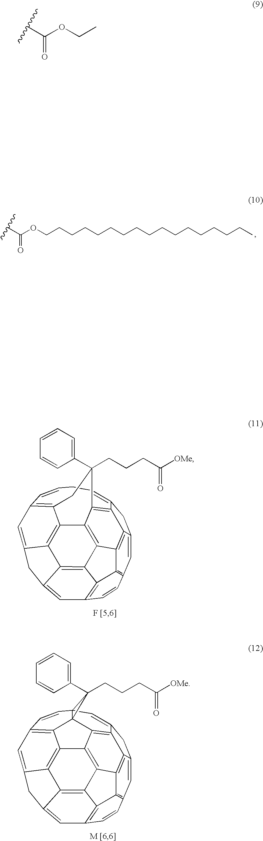


Applications Claiming Priority (2)
| Application Number | Priority Date | Filing Date | Title |
|---|---|---|---|
| KR2005-11405 | 2005-02-07 | ||
| KR1020050011405A KR20060090483A (en) | 2005-02-07 | 2005-02-07 | Composition for forming low dieletric film comprising fullerenes, low dielectric film using the composition and method for forming the low dielectric film |
Publications (1)
| Publication Number | Publication Date |
|---|---|
| US20060175685A1 true US20060175685A1 (en) | 2006-08-10 |
Family
ID=36779111
Family Applications (1)
| Application Number | Title | Priority Date | Filing Date |
|---|---|---|---|
| US11/347,238 Abandoned US20060175685A1 (en) | 2005-02-07 | 2006-02-06 | Composition for forming low-dielectric constant film comprising fullerene, low-dielectric constant film formed from the composition and method for forming the low-dielectric constant film |
Country Status (2)
| Country | Link |
|---|---|
| US (1) | US20060175685A1 (en) |
| KR (1) | KR20060090483A (en) |
Cited By (8)
| Publication number | Priority date | Publication date | Assignee | Title |
|---|---|---|---|---|
| US20070128879A1 (en) * | 2004-02-18 | 2007-06-07 | Industry-University Corporation Foundation Sogang University | Reactive cyclodextrin derivatives as pore-forming templates, and low dielectric materials prepared by using the same |
| US20070292700A1 (en) * | 2006-05-31 | 2007-12-20 | Roskilde Semiconductor Llc | Porous materials derived from polymer composites |
| US20080020197A1 (en) * | 2006-05-31 | 2008-01-24 | Roskilde Semiconductor Llc | Porous inorganic solids for use as low dielectric constant materials |
| US20080108774A1 (en) * | 2006-05-31 | 2008-05-08 | Roskilde Semiconductor Llc | Linked periodic networks of alternating carbon and inorganic clusters for use as low dielectric constant materials |
| US20090192281A1 (en) * | 2005-02-24 | 2009-07-30 | Michael Raymond Ayers | Porous Films and Bodies with Enhanced Mechanical Strength |
| US20150010703A1 (en) * | 2012-02-10 | 2015-01-08 | The University Of Birmingham | Spin on Hard-Mask Material |
| CN109054392A (en) * | 2018-05-28 | 2018-12-21 | 佛山市三水铠潮材料科技有限公司 | A kind of high thermal conductive silicon rubber composition |
| US10544329B2 (en) | 2015-04-13 | 2020-01-28 | Honeywell International Inc. | Polysiloxane formulations and coatings for optoelectronic applications |
Families Citing this family (2)
| Publication number | Priority date | Publication date | Assignee | Title |
|---|---|---|---|---|
| KR100931676B1 (en) * | 2008-04-08 | 2009-12-14 | 한국화학연구원 | C70 fullerene derivative and organic photovoltaic device using the same |
| KR101499144B1 (en) * | 2013-10-11 | 2015-03-06 | 전남대학교산학협력단 | Fullerene-embedded organosiloxane polymer having controlled refractive index and the manufacturing method of it |
Citations (20)
| Publication number | Priority date | Publication date | Assignee | Title |
|---|---|---|---|---|
| US3481898A (en) * | 1967-04-10 | 1969-12-02 | Midland Silicones Ltd | Polymerization of siloxanes |
| US3615272A (en) * | 1968-11-04 | 1971-10-26 | Dow Corning | Condensed soluble hydrogensilsesquioxane resin |
| US4399266A (en) * | 1980-08-26 | 1983-08-16 | Japan Synthetic Rubber Co., Ltd. | Laddery lower alkylpolysilsesquioxane having heat-resistant thin film-formability and process for preparing same |
| US4999397A (en) * | 1989-07-28 | 1991-03-12 | Dow Corning Corporation | Metastable silane hydrolyzates and process for their preparation |
| US5744399A (en) * | 1995-11-13 | 1998-04-28 | Lsi Logic Corporation | Process for forming low dielectric constant layers using fullerenes |
| US5965679A (en) * | 1996-09-10 | 1999-10-12 | The Dow Chemical Company | Polyphenylene oligomers and polymers |
| US6093636A (en) * | 1998-07-08 | 2000-07-25 | International Business Machines Corporation | Process for manufacture of integrated circuit device using a matrix comprising porous high temperature thermosets |
| US6107357A (en) * | 1999-11-16 | 2000-08-22 | International Business Machines Corporatrion | Dielectric compositions and method for their manufacture |
| US6204202B1 (en) * | 1999-04-14 | 2001-03-20 | Alliedsignal, Inc. | Low dielectric constant porous films |
| US6231989B1 (en) * | 1998-11-20 | 2001-05-15 | Dow Corning Corporation | Method of forming coatings |
| US6287979B1 (en) * | 2000-04-17 | 2001-09-11 | Chartered Semiconductor Manufacturing Ltd. | Method for forming an air gap as low dielectric constant material using buckminsterfullerene as a porogen in an air bridge or a sacrificial layer |
| US6406794B1 (en) * | 2001-02-08 | 2002-06-18 | Jsr Corporation | Film-forming composition |
| US6413882B1 (en) * | 1999-04-14 | 2002-07-02 | Alliedsignal Inc. | Low dielectric foam dielectric formed from polymer decomposition |
| US6423770B1 (en) * | 1999-07-15 | 2002-07-23 | Lucent Technologies Inc. | Silicate material and process for fabricating silicate material |
| US20030187139A1 (en) * | 2000-04-07 | 2003-10-02 | Kreisler Lau | Low dielectric constant organic dielectrics based on cage-like structures |
| US20040121501A1 (en) * | 2002-12-18 | 2004-06-24 | Large Jeffrey L. | Low dielectric constant interconnect insulator having fullerene additive |
| US20040242013A1 (en) * | 2003-06-02 | 2004-12-02 | Lyu Yi Yeol | Siloxane-based resin and interlayer insulating film for a semiconductor device made using the same |
| US20040247896A1 (en) * | 2001-12-31 | 2004-12-09 | Paul Apen | Organic compositions |
| US20050287818A1 (en) * | 2004-06-21 | 2005-12-29 | Nat Inst Of Adv Industrial Sci And Tech | Material and method for forming low-dielectric-constant film |
| US7186781B2 (en) * | 2002-10-02 | 2007-03-06 | Nitto Denko Corporation | Fullerene-containing polymer, producing method thereof, and photorefractive composition |
-
2005
- 2005-02-07 KR KR1020050011405A patent/KR20060090483A/en not_active Application Discontinuation
-
2006
- 2006-02-06 US US11/347,238 patent/US20060175685A1/en not_active Abandoned
Patent Citations (20)
| Publication number | Priority date | Publication date | Assignee | Title |
|---|---|---|---|---|
| US3481898A (en) * | 1967-04-10 | 1969-12-02 | Midland Silicones Ltd | Polymerization of siloxanes |
| US3615272A (en) * | 1968-11-04 | 1971-10-26 | Dow Corning | Condensed soluble hydrogensilsesquioxane resin |
| US4399266A (en) * | 1980-08-26 | 1983-08-16 | Japan Synthetic Rubber Co., Ltd. | Laddery lower alkylpolysilsesquioxane having heat-resistant thin film-formability and process for preparing same |
| US4999397A (en) * | 1989-07-28 | 1991-03-12 | Dow Corning Corporation | Metastable silane hydrolyzates and process for their preparation |
| US5744399A (en) * | 1995-11-13 | 1998-04-28 | Lsi Logic Corporation | Process for forming low dielectric constant layers using fullerenes |
| US5965679A (en) * | 1996-09-10 | 1999-10-12 | The Dow Chemical Company | Polyphenylene oligomers and polymers |
| US6093636A (en) * | 1998-07-08 | 2000-07-25 | International Business Machines Corporation | Process for manufacture of integrated circuit device using a matrix comprising porous high temperature thermosets |
| US6231989B1 (en) * | 1998-11-20 | 2001-05-15 | Dow Corning Corporation | Method of forming coatings |
| US6204202B1 (en) * | 1999-04-14 | 2001-03-20 | Alliedsignal, Inc. | Low dielectric constant porous films |
| US6413882B1 (en) * | 1999-04-14 | 2002-07-02 | Alliedsignal Inc. | Low dielectric foam dielectric formed from polymer decomposition |
| US6423770B1 (en) * | 1999-07-15 | 2002-07-23 | Lucent Technologies Inc. | Silicate material and process for fabricating silicate material |
| US6107357A (en) * | 1999-11-16 | 2000-08-22 | International Business Machines Corporatrion | Dielectric compositions and method for their manufacture |
| US20030187139A1 (en) * | 2000-04-07 | 2003-10-02 | Kreisler Lau | Low dielectric constant organic dielectrics based on cage-like structures |
| US6287979B1 (en) * | 2000-04-17 | 2001-09-11 | Chartered Semiconductor Manufacturing Ltd. | Method for forming an air gap as low dielectric constant material using buckminsterfullerene as a porogen in an air bridge or a sacrificial layer |
| US6406794B1 (en) * | 2001-02-08 | 2002-06-18 | Jsr Corporation | Film-forming composition |
| US20040247896A1 (en) * | 2001-12-31 | 2004-12-09 | Paul Apen | Organic compositions |
| US7186781B2 (en) * | 2002-10-02 | 2007-03-06 | Nitto Denko Corporation | Fullerene-containing polymer, producing method thereof, and photorefractive composition |
| US20040121501A1 (en) * | 2002-12-18 | 2004-06-24 | Large Jeffrey L. | Low dielectric constant interconnect insulator having fullerene additive |
| US20040242013A1 (en) * | 2003-06-02 | 2004-12-02 | Lyu Yi Yeol | Siloxane-based resin and interlayer insulating film for a semiconductor device made using the same |
| US20050287818A1 (en) * | 2004-06-21 | 2005-12-29 | Nat Inst Of Adv Industrial Sci And Tech | Material and method for forming low-dielectric-constant film |
Cited By (13)
| Publication number | Priority date | Publication date | Assignee | Title |
|---|---|---|---|---|
| US7462659B2 (en) * | 2004-02-18 | 2008-12-09 | Industry - University Cooperation Foundation Sogang University | Reactive cyclodextrin derivatives as pore-forming templates, and low dielectric materials prepared by using the same |
| US20070128879A1 (en) * | 2004-02-18 | 2007-06-07 | Industry-University Corporation Foundation Sogang University | Reactive cyclodextrin derivatives as pore-forming templates, and low dielectric materials prepared by using the same |
| US8034890B2 (en) | 2005-02-24 | 2011-10-11 | Roskilde Semiconductor Llc | Porous films and bodies with enhanced mechanical strength |
| US20090192281A1 (en) * | 2005-02-24 | 2009-07-30 | Michael Raymond Ayers | Porous Films and Bodies with Enhanced Mechanical Strength |
| US20080108774A1 (en) * | 2006-05-31 | 2008-05-08 | Roskilde Semiconductor Llc | Linked periodic networks of alternating carbon and inorganic clusters for use as low dielectric constant materials |
| US20080020197A1 (en) * | 2006-05-31 | 2008-01-24 | Roskilde Semiconductor Llc | Porous inorganic solids for use as low dielectric constant materials |
| US7875315B2 (en) | 2006-05-31 | 2011-01-25 | Roskilde Semiconductor Llc | Porous inorganic solids for use as low dielectric constant materials |
| US7883742B2 (en) * | 2006-05-31 | 2011-02-08 | Roskilde Semiconductor Llc | Porous materials derived from polymer composites |
| US7919188B2 (en) | 2006-05-31 | 2011-04-05 | Roskilde Semiconductor Llc | Linked periodic networks of alternating carbon and inorganic clusters for use as low dielectric constant materials |
| US20070292700A1 (en) * | 2006-05-31 | 2007-12-20 | Roskilde Semiconductor Llc | Porous materials derived from polymer composites |
| US20150010703A1 (en) * | 2012-02-10 | 2015-01-08 | The University Of Birmingham | Spin on Hard-Mask Material |
| US10544329B2 (en) | 2015-04-13 | 2020-01-28 | Honeywell International Inc. | Polysiloxane formulations and coatings for optoelectronic applications |
| CN109054392A (en) * | 2018-05-28 | 2018-12-21 | 佛山市三水铠潮材料科技有限公司 | A kind of high thermal conductive silicon rubber composition |
Also Published As
| Publication number | Publication date |
|---|---|
| KR20060090483A (en) | 2006-08-11 |
Similar Documents
| Publication | Publication Date | Title |
|---|---|---|
| US20060175685A1 (en) | Composition for forming low-dielectric constant film comprising fullerene, low-dielectric constant film formed from the composition and method for forming the low-dielectric constant film | |
| US8053173B2 (en) | Multi-functional linear siloxane compound, a siloxane polymer prepared from the compound, and a process for forming a dielectric film by using the polymer | |
| JP4090244B2 (en) | Composition for producing a substance having nanopores | |
| US7294584B2 (en) | Siloxane-based resin and a semiconductor interlayer insulating film using the same | |
| US7470634B2 (en) | Method for forming interlayer dielectric film for semiconductor device by using polyhedral molecular silsesquioxane | |
| US7374820B2 (en) | Siloxane-based resin containing germanium and an interlayer insulating film for a semiconductor device using the same | |
| US20060145306A1 (en) | Composition for forming low dielectric thin film comprising porous nanoparticles and method of preparing low dielectric thin film using the same | |
| US20050090570A1 (en) | Composition for forming dielectric film and method for forming dielectric film or pattern using the composition | |
| US7338689B2 (en) | Composition for forming low dielectric thin film including siloxane monomer or siloxane polymer having only one type of stereoisomer and method of producing low dielectric thin film using same | |
| JP2002363285A (en) | Siloxane-based resin and method for forming semiconductor interlayer insulating film by using the same | |
| US20060110940A1 (en) | Method of preparing mesoporous thin film having low dielectric constant | |
| US20050049382A1 (en) | Novel siloxane-based resin and interlayer insulating film formed using the same | |
| US7144453B2 (en) | Composition for preparing porous dielectric thin film containing saccharides porogen | |
| US7169477B2 (en) | Composition for preparing porous dielectric thin films | |
| US6632748B2 (en) | Composition for preparing substances having nano-pores | |
| US20060134441A1 (en) | Siloxane-based polymer and method for forming dielectric film using the polymer | |
| US20040242013A1 (en) | Siloxane-based resin and interlayer insulating film for a semiconductor device made using the same | |
| EP1412434B1 (en) | Siloxane resins | |
| US6908977B2 (en) | Siloxane-based resin and method of forming an insulating film between interconnect layers of a semiconductor device using the same | |
| US7459549B2 (en) | Composition for preparing nanoporous material | |
| US7517917B2 (en) | Composition for preparing nanoporous material comprising calixarene derivative | |
| US20060135633A1 (en) | Porous low-dielectric constant (k) thin film with controlled solvent diffusion | |
| US20070027225A1 (en) | Composition for preparing porous dielectric thin films | |
| Lyu et al. | Effect of the linear siloxane chain in cyclic silsesquioxane (CSSQ) on the mechanical/electrical property of the thin films |
Legal Events
| Date | Code | Title | Description |
|---|---|---|---|
| AS | Assignment |
Owner name: SAMSUNG CORNING CO., LTD., KOREA, REPUBLIC OF Free format text: ASSIGNMENT OF ASSIGNORS INTEREST;ASSIGNORS:SHIN, HYEONG JIN;JEONG, HYUN DAM;SEON, JONG BAEK;REEL/FRAME:017421/0011 Effective date: 20060207 |
|
| AS | Assignment |
Owner name: SAMSUNG CORNING CO., LTD., KOREA, REPUBLIC OF Free format text: MERGER;ASSIGNOR:SAMSUNG CORNING PRECISION GLASS CO., LTD.;REEL/FRAME:020624/0240 Effective date: 20080103 Owner name: SAMSUNG CORNING CO., LTD.,KOREA, REPUBLIC OF Free format text: MERGER;ASSIGNOR:SAMSUNG CORNING PRECISION GLASS CO., LTD.;REEL/FRAME:020624/0240 Effective date: 20080103 |
|
| AS | Assignment |
Owner name: SAMSUNG CORNING PRECISION GLASS CO., LTD., KOREA, Free format text: CORRECTIVE ASSIGNMENT TO CORRECT THE ASSIGNEE/ASSIGNOR PREVIOUSLY RECORDED ON REEL 020624 FRAME 0240. ASSIGNOR(S) HEREBY CONFIRMS THE MERGER.;ASSIGNOR:SAMSUNG CORNING CO., LTD.;REEL/FRAME:020956/0832 Effective date: 20080306 Owner name: SAMSUNG CORNING PRECISION GLASS CO., LTD.,KOREA, R Free format text: CORRECTIVE ASSIGNMENT TO CORRECT THE ASSIGNEE/ASSIGNOR PREVIOUSLY RECORDED ON REEL 020624 FRAME 0240. ASSIGNOR(S) HEREBY CONFIRMS THE MERGER;ASSIGNOR:SAMSUNG CORNING CO., LTD.;REEL/FRAME:020956/0832 Effective date: 20080306 Owner name: SAMSUNG CORNING PRECISION GLASS CO., LTD., KOREA, Free format text: CORRECTIVE ASSIGNMENT TO CORRECT THE ASSIGNEE/ASSIGNOR PREVIOUSLY RECORDED ON REEL 020624 FRAME 0240. ASSIGNOR(S) HEREBY CONFIRMS THE MERGER;ASSIGNOR:SAMSUNG CORNING CO., LTD.;REEL/FRAME:020956/0832 Effective date: 20080306 |
|
| STCB | Information on status: application discontinuation |
Free format text: ABANDONED -- FAILURE TO RESPOND TO AN OFFICE ACTION |