US20070235725A1 - Ethynylene acene polymers and electronic devices generated therefrom - Google Patents
Ethynylene acene polymers and electronic devices generated therefrom Download PDFInfo
- Publication number
- US20070235725A1 US20070235725A1 US11/399,169 US39916906A US2007235725A1 US 20070235725 A1 US20070235725 A1 US 20070235725A1 US 39916906 A US39916906 A US 39916906A US 2007235725 A1 US2007235725 A1 US 2007235725A1
- Authority
- US
- United States
- Prior art keywords
- accordance
- zero
- independently represents
- polymer
- sum
- Prior art date
- Legal status (The legal status is an assumption and is not a legal conclusion. Google has not performed a legal analysis and makes no representation as to the accuracy of the status listed.)
- Granted
Links
- 229920000642 polymer Polymers 0.000 title claims abstract description 59
- -1 Ethynylene acene Chemical compound 0.000 title claims description 208
- 229920003026 Acene Polymers 0.000 title claims description 46
- 229910052786 argon Inorganic materials 0.000 claims abstract description 22
- 125000003118 aryl group Chemical group 0.000 claims abstract description 22
- 229930195733 hydrocarbon Natural products 0.000 claims abstract description 15
- 150000002430 hydrocarbons Chemical class 0.000 claims abstract description 14
- 239000004215 Carbon black (E152) Substances 0.000 claims abstract description 13
- 125000005842 heteroatom Chemical group 0.000 claims abstract description 11
- 229910052736 halogen Inorganic materials 0.000 claims abstract description 10
- 150000002367 halogens Chemical class 0.000 claims abstract description 10
- 125000004435 hydrogen atom Chemical class [H]* 0.000 claims abstract description 10
- 239000001257 hydrogen Substances 0.000 claims abstract description 9
- 229910052739 hydrogen Inorganic materials 0.000 claims abstract description 9
- 239000004065 semiconductor Substances 0.000 claims description 30
- 239000000758 substrate Substances 0.000 claims description 19
- 239000010409 thin film Substances 0.000 claims description 19
- 125000004432 carbon atom Chemical group C* 0.000 claims description 17
- 125000000217 alkyl group Chemical group 0.000 claims description 13
- 125000003545 alkoxy group Chemical group 0.000 claims description 11
- 238000000034 method Methods 0.000 claims description 11
- 229910052760 oxygen Inorganic materials 0.000 claims description 11
- 238000007639 printing Methods 0.000 claims description 11
- 230000008569 process Effects 0.000 claims description 10
- 238000004528 spin coating Methods 0.000 claims description 8
- 229920001940 conductive polymer Polymers 0.000 claims description 7
- 230000005669 field effect Effects 0.000 claims description 7
- RMSGQZDGSZOJMU-UHFFFAOYSA-N 1-butyl-2-phenylbenzene Chemical group CCCCC1=CC=CC=C1C1=CC=CC=C1 RMSGQZDGSZOJMU-UHFFFAOYSA-N 0.000 claims description 6
- SNRUBQQJIBEYMU-UHFFFAOYSA-N Dodecane Natural products CCCCCCCCCCCC SNRUBQQJIBEYMU-UHFFFAOYSA-N 0.000 claims description 6
- PXHVJJICTQNCMI-UHFFFAOYSA-N Nickel Chemical compound [Ni] PXHVJJICTQNCMI-UHFFFAOYSA-N 0.000 claims description 6
- 239000004642 Polyimide Substances 0.000 claims description 6
- 125000000484 butyl group Chemical group [H]C([*])([H])C([H])([H])C([H])([H])C([H])([H])[H] 0.000 claims description 6
- 125000002704 decyl group Chemical group [H]C([H])([H])C([H])([H])C([H])([H])C([H])([H])C([H])([H])C([H])([H])C([H])([H])C([H])([H])C([H])([H])C([H])([H])* 0.000 claims description 6
- 125000003438 dodecyl group Chemical group [H]C([H])([H])C([H])([H])C([H])([H])C([H])([H])C([H])([H])C([H])([H])C([H])([H])C([H])([H])C([H])([H])C([H])([H])C([H])([H])C([H])([H])* 0.000 claims description 6
- 125000003187 heptyl group Chemical group [H]C([*])([H])C([H])([H])C([H])([H])C([H])([H])C([H])([H])C([H])([H])C([H])([H])[H] 0.000 claims description 6
- 125000004051 hexyl group Chemical group [H]C([H])([H])C([H])([H])C([H])([H])C([H])([H])C([H])([H])C([H])([H])* 0.000 claims description 6
- 125000002960 margaryl group Chemical group [H]C([*])([H])C([H])([H])C([H])([H])C([H])([H])C([H])([H])C([H])([H])C([H])([H])C([H])([H])C([H])([H])C([H])([H])C([H])([H])C([H])([H])C([H])([H])C([H])([H])C([H])([H])C([H])([H])C([H])([H])[H] 0.000 claims description 6
- 125000001421 myristyl group Chemical group [H]C([*])([H])C([H])([H])C([H])([H])C([H])([H])C([H])([H])C([H])([H])C([H])([H])C([H])([H])C([H])([H])C([H])([H])C([H])([H])C([H])([H])C([H])([H])C([H])([H])[H] 0.000 claims description 6
- 125000001400 nonyl group Chemical group [H]C([*])([H])C([H])([H])C([H])([H])C([H])([H])C([H])([H])C([H])([H])C([H])([H])C([H])([H])C([H])([H])[H] 0.000 claims description 6
- 125000002347 octyl group Chemical group [H]C([*])([H])C([H])([H])C([H])([H])C([H])([H])C([H])([H])C([H])([H])C([H])([H])C([H])([H])[H] 0.000 claims description 6
- 125000000913 palmityl group Chemical group [H]C([*])([H])C([H])([H])C([H])([H])C([H])([H])C([H])([H])C([H])([H])C([H])([H])C([H])([H])C([H])([H])C([H])([H])C([H])([H])C([H])([H])C([H])([H])C([H])([H])C([H])([H])C([H])([H])[H] 0.000 claims description 6
- 125000002958 pentadecyl group Chemical group [H]C([*])([H])C([H])([H])C([H])([H])C([H])([H])C([H])([H])C([H])([H])C([H])([H])C([H])([H])C([H])([H])C([H])([H])C([H])([H])C([H])([H])C([H])([H])C([H])([H])C([H])([H])[H] 0.000 claims description 6
- 125000001147 pentyl group Chemical group C(CCCC)* 0.000 claims description 6
- BASFCYQUMIYNBI-UHFFFAOYSA-N platinum Chemical compound [Pt] BASFCYQUMIYNBI-UHFFFAOYSA-N 0.000 claims description 6
- 229920000728 polyester Polymers 0.000 claims description 6
- 229920001721 polyimide Polymers 0.000 claims description 6
- 125000004079 stearyl group Chemical group [H]C([*])([H])C([H])([H])C([H])([H])C([H])([H])C([H])([H])C([H])([H])C([H])([H])C([H])([H])C([H])([H])C([H])([H])C([H])([H])C([H])([H])C([H])([H])C([H])([H])C([H])([H])C([H])([H])C([H])([H])C([H])([H])[H] 0.000 claims description 6
- 125000002889 tridecyl group Chemical group [H]C([*])([H])C([H])([H])C([H])([H])C([H])([H])C([H])([H])C([H])([H])C([H])([H])C([H])([H])C([H])([H])C([H])([H])C([H])([H])C([H])([H])C([H])([H])[H] 0.000 claims description 6
- 125000002948 undecyl group Chemical group [H]C([*])([H])C([H])([H])C([H])([H])C([H])([H])C([H])([H])C([H])([H])C([H])([H])C([H])([H])C([H])([H])C([H])([H])C([H])([H])[H] 0.000 claims description 6
- XFXPMWWXUTWYJX-UHFFFAOYSA-N Cyanide Chemical group N#[C-] XFXPMWWXUTWYJX-UHFFFAOYSA-N 0.000 claims description 5
- JCXJVPUVTGWSNB-UHFFFAOYSA-N Nitrogen dioxide Chemical group O=[N]=O JCXJVPUVTGWSNB-UHFFFAOYSA-N 0.000 claims description 5
- 239000000460 chlorine Substances 0.000 claims description 5
- PCHJSUWPFVWCPO-UHFFFAOYSA-N gold Chemical compound [Au] PCHJSUWPFVWCPO-UHFFFAOYSA-N 0.000 claims description 5
- 229910052737 gold Inorganic materials 0.000 claims description 5
- 239000010931 gold Substances 0.000 claims description 5
- 229920000620 organic polymer Polymers 0.000 claims description 5
- 239000002985 plastic film Substances 0.000 claims description 5
- 229920000515 polycarbonate Polymers 0.000 claims description 5
- 239000004417 polycarbonate Substances 0.000 claims description 5
- VYPSYNLAJGMNEJ-UHFFFAOYSA-N Silicium dioxide Chemical compound O=[Si]=O VYPSYNLAJGMNEJ-UHFFFAOYSA-N 0.000 claims description 4
- BQCADISMDOOEFD-UHFFFAOYSA-N Silver Chemical compound [Ag] BQCADISMDOOEFD-UHFFFAOYSA-N 0.000 claims description 4
- 229910052782 aluminium Inorganic materials 0.000 claims description 4
- XAGFODPZIPBFFR-UHFFFAOYSA-N aluminium Chemical compound [Al] XAGFODPZIPBFFR-UHFFFAOYSA-N 0.000 claims description 4
- 229910052799 carbon Inorganic materials 0.000 claims description 4
- 229910052731 fluorine Inorganic materials 0.000 claims description 4
- 238000007650 screen-printing Methods 0.000 claims description 4
- 229910052814 silicon oxide Inorganic materials 0.000 claims description 4
- 229910052581 Si3N4 Inorganic materials 0.000 claims description 3
- 125000004093 cyano group Chemical group *C#N 0.000 claims description 3
- 125000002496 methyl group Chemical group [H]C([H])([H])* 0.000 claims description 3
- 229910052759 nickel Inorganic materials 0.000 claims description 3
- 125000000449 nitro group Chemical group [O-][N+](*)=O 0.000 claims description 3
- 125000001997 phenyl group Chemical group [H]C1=C([H])C([H])=C(*)C([H])=C1[H] 0.000 claims description 3
- 229910052697 platinum Inorganic materials 0.000 claims description 3
- HQVNEWCFYHHQES-UHFFFAOYSA-N silicon nitride Chemical compound N12[Si]34N5[Si]62N3[Si]51N64 HQVNEWCFYHHQES-UHFFFAOYSA-N 0.000 claims description 3
- 229910052709 silver Inorganic materials 0.000 claims description 3
- 239000004332 silver Substances 0.000 claims description 3
- 125000000547 substituted alkyl group Chemical group 0.000 claims description 3
- 125000003107 substituted aryl group Chemical group 0.000 claims description 3
- 229910052717 sulfur Inorganic materials 0.000 claims description 3
- ZCYVEMRRCGMTRW-UHFFFAOYSA-N 7553-56-2 Chemical compound [I] ZCYVEMRRCGMTRW-UHFFFAOYSA-N 0.000 claims description 2
- WKBOTKDWSSQWDR-UHFFFAOYSA-N Bromine atom Chemical compound [Br] WKBOTKDWSSQWDR-UHFFFAOYSA-N 0.000 claims description 2
- ZAMOUSCENKQFHK-UHFFFAOYSA-N Chlorine atom Chemical compound [Cl] ZAMOUSCENKQFHK-UHFFFAOYSA-N 0.000 claims description 2
- VYZAMTAEIAYCRO-UHFFFAOYSA-N Chromium Chemical compound [Cr] VYZAMTAEIAYCRO-UHFFFAOYSA-N 0.000 claims description 2
- PXGOKWXKJXAPGV-UHFFFAOYSA-N Fluorine Chemical compound FF PXGOKWXKJXAPGV-UHFFFAOYSA-N 0.000 claims description 2
- 125000001204 arachidyl group Chemical group [H]C([*])([H])C([H])([H])C([H])([H])C([H])([H])C([H])([H])C([H])([H])C([H])([H])C([H])([H])C([H])([H])C([H])([H])C([H])([H])C([H])([H])C([H])([H])C([H])([H])C([H])([H])C([H])([H])C([H])([H])C([H])([H])C([H])([H])C([H])([H])[H] 0.000 claims description 2
- GDTBXPJZTBHREO-UHFFFAOYSA-N bromine Substances BrBr GDTBXPJZTBHREO-UHFFFAOYSA-N 0.000 claims description 2
- 229910052794 bromium Inorganic materials 0.000 claims description 2
- 229910052801 chlorine Inorganic materials 0.000 claims description 2
- 229910052804 chromium Inorganic materials 0.000 claims description 2
- 239000011651 chromium Substances 0.000 claims description 2
- 125000004986 diarylamino group Chemical group 0.000 claims description 2
- 239000011737 fluorine Substances 0.000 claims description 2
- BDVZHDCXCXJPSO-UHFFFAOYSA-N indium(3+) oxygen(2-) titanium(4+) Chemical compound [O-2].[Ti+4].[In+3] BDVZHDCXCXJPSO-UHFFFAOYSA-N 0.000 claims description 2
- 229910052740 iodine Inorganic materials 0.000 claims description 2
- 239000011630 iodine Substances 0.000 claims description 2
- 239000000203 mixture Substances 0.000 claims description 2
- 229910052757 nitrogen Inorganic materials 0.000 claims description 2
- 125000004433 nitrogen atom Chemical group N* 0.000 claims description 2
- 125000001196 nonadecyl group Chemical group [H]C([*])([H])C([H])([H])C([H])([H])C([H])([H])C([H])([H])C([H])([H])C([H])([H])C([H])([H])C([H])([H])C([H])([H])C([H])([H])C([H])([H])C([H])([H])C([H])([H])C([H])([H])C([H])([H])C([H])([H])C([H])([H])C([H])([H])[H] 0.000 claims description 2
- 125000005415 substituted alkoxy group Chemical group 0.000 claims description 2
- 125000003944 tolyl group Chemical group 0.000 claims description 2
- 125000004665 trialkylsilyl group Chemical group 0.000 claims description 2
- 125000005106 triarylsilyl group Chemical group 0.000 claims description 2
- 125000002306 tributylsilyl group Chemical group C(CCC)[Si](CCCC)(CCCC)* 0.000 claims description 2
- 125000002023 trifluoromethyl group Chemical group FC(F)(F)* 0.000 claims description 2
- 125000000026 trimethylsilyl group Chemical group [H]C([H])([H])[Si]([*])(C([H])([H])[H])C([H])([H])[H] 0.000 claims description 2
- 125000001183 hydrocarbyl group Chemical group 0.000 claims 2
- 150000004767 nitrides Chemical class 0.000 claims 1
- 239000000463 material Substances 0.000 description 18
- YMWUJEATGCHHMB-UHFFFAOYSA-N Dichloromethane Chemical compound ClCCl YMWUJEATGCHHMB-UHFFFAOYSA-N 0.000 description 9
- QVGXLLKOCUKJST-UHFFFAOYSA-N atomic oxygen Chemical compound [O] QVGXLLKOCUKJST-UHFFFAOYSA-N 0.000 description 9
- 239000001301 oxygen Substances 0.000 description 9
- XUIMIQQOPSSXEZ-UHFFFAOYSA-N Silicon Chemical compound [Si] XUIMIQQOPSSXEZ-UHFFFAOYSA-N 0.000 description 8
- WYURNTSHIVDZCO-UHFFFAOYSA-N Tetrahydrofuran Chemical compound C1CCOC1 WYURNTSHIVDZCO-UHFFFAOYSA-N 0.000 description 8
- 229910052710 silicon Inorganic materials 0.000 description 8
- 239000010703 silicon Substances 0.000 description 8
- 239000010408 film Substances 0.000 description 7
- YXFVVABEGXRONW-UHFFFAOYSA-N Toluene Chemical compound CC1=CC=CC=C1 YXFVVABEGXRONW-UHFFFAOYSA-N 0.000 description 6
- 239000000976 ink Substances 0.000 description 6
- 238000004519 manufacturing process Methods 0.000 description 6
- 229910052751 metal Inorganic materials 0.000 description 6
- 239000002184 metal Substances 0.000 description 6
- RIOQSEWOXXDEQQ-UHFFFAOYSA-N triphenylphosphine Chemical compound C1=CC=CC=C1P(C=1C=CC=CC=1)C1=CC=CC=C1 RIOQSEWOXXDEQQ-UHFFFAOYSA-N 0.000 description 6
- ZMXDDKWLCZADIW-UHFFFAOYSA-N N,N-Dimethylformamide Chemical compound CN(C)C=O ZMXDDKWLCZADIW-UHFFFAOYSA-N 0.000 description 5
- ZMANZCXQSJIPKH-UHFFFAOYSA-N Triethylamine Chemical compound CCN(CC)CC ZMANZCXQSJIPKH-UHFFFAOYSA-N 0.000 description 5
- 239000002904 solvent Substances 0.000 description 5
- XKRFYHLGVUSROY-UHFFFAOYSA-N Argon Chemical compound [Ar] XKRFYHLGVUSROY-UHFFFAOYSA-N 0.000 description 4
- JRNVZBWKYDBUCA-UHFFFAOYSA-N N-chlorosuccinimide Chemical compound ClN1C(=O)CCC1=O JRNVZBWKYDBUCA-UHFFFAOYSA-N 0.000 description 4
- 238000005266 casting Methods 0.000 description 4
- MVPPADPHJFYWMZ-UHFFFAOYSA-N chlorobenzene Chemical compound ClC1=CC=CC=C1 MVPPADPHJFYWMZ-UHFFFAOYSA-N 0.000 description 4
- 150000001875 compounds Chemical class 0.000 description 4
- 239000002322 conducting polymer Substances 0.000 description 4
- 238000013461 design Methods 0.000 description 4
- 238000004377 microelectronic Methods 0.000 description 4
- 230000001590 oxidative effect Effects 0.000 description 4
- YLQBMQCUIZJEEH-UHFFFAOYSA-N tetrahydrofuran Natural products C=1C=COC=1 YLQBMQCUIZJEEH-UHFFFAOYSA-N 0.000 description 4
- MXZLGYMOFAZTNN-UHFFFAOYSA-N 2-bromo-5-chloro-3-dodecylthiophene Chemical compound CCCCCCCCCCCCC=1C=C(Cl)SC=1Br MXZLGYMOFAZTNN-UHFFFAOYSA-N 0.000 description 3
- OKKJLVBELUTLKV-UHFFFAOYSA-N Methanol Chemical compound OC OKKJLVBELUTLKV-UHFFFAOYSA-N 0.000 description 3
- 229920001609 Poly(3,4-ethylenedioxythiophene) Polymers 0.000 description 3
- 239000004793 Polystyrene Substances 0.000 description 3
- 239000002131 composite material Substances 0.000 description 3
- 238000005516 engineering process Methods 0.000 description 3
- 239000011521 glass Substances 0.000 description 3
- SLIUAWYAILUBJU-UHFFFAOYSA-N pentacene Chemical compound C1=CC=CC2=CC3=CC4=CC5=CC=CC=C5C=C4C=C3C=C21 SLIUAWYAILUBJU-UHFFFAOYSA-N 0.000 description 3
- 239000004033 plastic Substances 0.000 description 3
- 229920003023 plastic Polymers 0.000 description 3
- 229920002223 polystyrene Polymers 0.000 description 3
- WSLDOOZREJYCGB-UHFFFAOYSA-N 1,2-Dichloroethane Chemical compound ClCCCl WSLDOOZREJYCGB-UHFFFAOYSA-N 0.000 description 2
- HELFMPIITDWHAL-UHFFFAOYSA-N 2-(5-chloro-3-dodecylthiophen-2-yl)ethynyl-trimethylsilane Chemical compound CCCCCCCCCCCCC=1C=C(Cl)SC=1C#C[Si](C)(C)C HELFMPIITDWHAL-UHFFFAOYSA-N 0.000 description 2
- CRUBBCQEXCJEDL-UHFFFAOYSA-N 3-dodecyl-2-[2-[10-[2-(3-dodecylthiophen-2-yl)ethynyl]anthracen-9-yl]ethynyl]thiophene Chemical compound C1=CSC(C#CC=2C3=CC=CC=C3C(C#CC3=C(C=CS3)CCCCCCCCCCCC)=C3C=CC=CC3=2)=C1CCCCCCCCCCCC CRUBBCQEXCJEDL-UHFFFAOYSA-N 0.000 description 2
- YQGODCPVRNYYHE-UHFFFAOYSA-N 3-dodecyl-2-[2-[13-[2-(3-dodecylthiophen-2-yl)ethynyl]pentacen-6-yl]ethynyl]thiophene Chemical compound C1=CSC(C#CC=2C3=CC4=CC=CC=C4C=C3C(C#CC3=C(C=CS3)CCCCCCCCCCCC)=C3C=C4C=CC=CC4=CC3=2)=C1CCCCCCCCCCCC YQGODCPVRNYYHE-UHFFFAOYSA-N 0.000 description 2
- YPNJCUPXRCTBOF-UHFFFAOYSA-N 5-chloro-2-[2-[10-[2-(5-chloro-3-dodecylthiophen-2-yl)ethynyl]anthracen-9-yl]ethynyl]-3-dodecylthiophene Chemical compound C1=C(Cl)SC(C#CC=2C3=CC=CC=C3C(C#CC3=C(C=C(Cl)S3)CCCCCCCCCCCC)=C3C=CC=CC3=2)=C1CCCCCCCCCCCC YPNJCUPXRCTBOF-UHFFFAOYSA-N 0.000 description 2
- QOZNNUONEAEKNM-UHFFFAOYSA-N 5-chloro-2-[2-[13-[2-(5-chloro-3-dodecylthiophen-2-yl)ethynyl]pentacen-6-yl]ethynyl]-3-dodecylthiophene Chemical compound C1=C(Cl)SC(C#CC=2C3=CC4=CC=CC=C4C=C3C(C#CC3=C(C=C(Cl)S3)CCCCCCCCCCCC)=C3C=C4C=CC=CC4=CC3=2)=C1CCCCCCCCCCCC QOZNNUONEAEKNM-UHFFFAOYSA-N 0.000 description 2
- WOGXYDPPRVOQOF-UHFFFAOYSA-N 5-chloro-3-dodecyl-2-ethynylthiophene Chemical compound CCCCCCCCCCCCC=1C=C(Cl)SC=1C#C WOGXYDPPRVOQOF-UHFFFAOYSA-N 0.000 description 2
- 229910021595 Copper(I) iodide Inorganic materials 0.000 description 2
- FXHOOIRPVKKKFG-UHFFFAOYSA-N N,N-Dimethylacetamide Chemical compound CN(C)C(C)=O FXHOOIRPVKKKFG-UHFFFAOYSA-N 0.000 description 2
- 229910021586 Nickel(II) chloride Inorganic materials 0.000 description 2
- CTQNGGLPUBDAKN-UHFFFAOYSA-N O-Xylene Chemical compound CC1=CC=CC=C1C CTQNGGLPUBDAKN-UHFFFAOYSA-N 0.000 description 2
- YTPLMLYBLZKORZ-UHFFFAOYSA-N Thiophene Chemical compound C=1C=CSC=1 YTPLMLYBLZKORZ-UHFFFAOYSA-N 0.000 description 2
- 229910021626 Tin(II) chloride Inorganic materials 0.000 description 2
- 230000002411 adverse Effects 0.000 description 2
- MWPLVEDNUUSJAV-UHFFFAOYSA-N anthracene Chemical class C1=CC=CC2=CC3=CC=CC=C3C=C21 MWPLVEDNUUSJAV-UHFFFAOYSA-N 0.000 description 2
- 150000004982 aromatic amines Chemical class 0.000 description 2
- 239000002800 charge carrier Substances 0.000 description 2
- 239000011248 coating agent Substances 0.000 description 2
- 238000000576 coating method Methods 0.000 description 2
- 239000003989 dielectric material Substances 0.000 description 2
- 239000006185 dispersion Substances 0.000 description 2
- 239000007772 electrode material Substances 0.000 description 2
- 239000003822 epoxy resin Substances 0.000 description 2
- 125000002534 ethynyl group Chemical group [H]C#C* 0.000 description 2
- 230000006870 function Effects 0.000 description 2
- VVVPGLRKXQSQSZ-UHFFFAOYSA-N indolo[3,2-c]carbazole Chemical group C1=CC=CC2=NC3=C4C5=CC=CC=C5N=C4C=CC3=C21 VVVPGLRKXQSQSZ-UHFFFAOYSA-N 0.000 description 2
- 229910010272 inorganic material Inorganic materials 0.000 description 2
- 239000011147 inorganic material Substances 0.000 description 2
- IUYHWZFSGMZEOG-UHFFFAOYSA-M magnesium;propane;chloride Chemical compound [Mg+2].[Cl-].C[CH-]C IUYHWZFSGMZEOG-UHFFFAOYSA-M 0.000 description 2
- AUHZEENZYGFFBQ-UHFFFAOYSA-N mesitylene Substances CC1=CC(C)=CC(C)=C1 AUHZEENZYGFFBQ-UHFFFAOYSA-N 0.000 description 2
- 125000001827 mesitylenyl group Chemical group [H]C1=C(C(*)=C(C([H])=C1C([H])([H])[H])C([H])([H])[H])C([H])([H])[H] 0.000 description 2
- 229910044991 metal oxide Inorganic materials 0.000 description 2
- 150000004706 metal oxides Chemical class 0.000 description 2
- QMMRZOWCJAIUJA-UHFFFAOYSA-L nickel dichloride Chemical compound Cl[Ni]Cl QMMRZOWCJAIUJA-UHFFFAOYSA-L 0.000 description 2
- 229920000647 polyepoxide Polymers 0.000 description 2
- 229920005596 polymer binder Polymers 0.000 description 2
- 239000002491 polymer binding agent Substances 0.000 description 2
- 229920000193 polymethacrylate Polymers 0.000 description 2
- BWHMMNNQKKPAPP-UHFFFAOYSA-L potassium carbonate Chemical compound [K+].[K+].[O-]C([O-])=O BWHMMNNQKKPAPP-UHFFFAOYSA-L 0.000 description 2
- 238000002360 preparation method Methods 0.000 description 2
- 238000012545 processing Methods 0.000 description 2
- 125000001424 substituent group Chemical group 0.000 description 2
- AXZWODMDQAVCJE-UHFFFAOYSA-L tin(II) chloride (anhydrous) Chemical compound [Cl-].[Cl-].[Sn+2] AXZWODMDQAVCJE-UHFFFAOYSA-L 0.000 description 2
- 238000001771 vacuum deposition Methods 0.000 description 2
- 239000008096 xylene Substances 0.000 description 2
- PIINXYKJQGMIOZ-UHFFFAOYSA-N 1,2-dipyridin-2-ylethane-1,2-dione Chemical compound C=1C=CC=NC=1C(=O)C(=O)C1=CC=CC=N1 PIINXYKJQGMIOZ-UHFFFAOYSA-N 0.000 description 1
- OCJBOOLMMGQPQU-UHFFFAOYSA-N 1,4-dichlorobenzene Chemical compound ClC1=CC=C(Cl)C=C1 OCJBOOLMMGQPQU-UHFFFAOYSA-N 0.000 description 1
- TZMSYXZUNZXBOL-UHFFFAOYSA-N 10H-phenoxazine Chemical compound C1=CC=C2NC3=CC=CC=C3OC2=C1 TZMSYXZUNZXBOL-UHFFFAOYSA-N 0.000 description 1
- IMILVTHOOISGRW-UHFFFAOYSA-N 2-bromo-3-dodecylthiophene Chemical compound CCCCCCCCCCCCC=1C=CSC=1Br IMILVTHOOISGRW-UHFFFAOYSA-N 0.000 description 1
- RFKWIEFTBMACPZ-UHFFFAOYSA-N 3-dodecylthiophene Chemical compound CCCCCCCCCCCCC=1C=CSC=1 RFKWIEFTBMACPZ-UHFFFAOYSA-N 0.000 description 1
- OKTJSMMVPCPJKN-UHFFFAOYSA-N Carbon Chemical compound [C] OKTJSMMVPCPJKN-UHFFFAOYSA-N 0.000 description 1
- PCLIMKBDDGJMGD-UHFFFAOYSA-N N-bromosuccinimide Chemical compound BrN1C(=O)CCC1=O PCLIMKBDDGJMGD-UHFFFAOYSA-N 0.000 description 1
- BUGBHKTXTAQXES-UHFFFAOYSA-N Selenium Chemical compound [Se] BUGBHKTXTAQXES-UHFFFAOYSA-N 0.000 description 1
- NINIDFKCEFEMDL-UHFFFAOYSA-N Sulfur Chemical compound [S] NINIDFKCEFEMDL-UHFFFAOYSA-N 0.000 description 1
- RTAQQCXQSZGOHL-UHFFFAOYSA-N Titanium Chemical compound [Ti] RTAQQCXQSZGOHL-UHFFFAOYSA-N 0.000 description 1
- HCHKCACWOHOZIP-UHFFFAOYSA-N Zinc Chemical compound [Zn] HCHKCACWOHOZIP-UHFFFAOYSA-N 0.000 description 1
- 238000000862 absorption spectrum Methods 0.000 description 1
- 125000002877 alkyl aryl group Chemical group 0.000 description 1
- 125000000304 alkynyl group Chemical group 0.000 description 1
- HSFWRNGVRCDJHI-UHFFFAOYSA-N alpha-acetylene Natural products C#C HSFWRNGVRCDJHI-UHFFFAOYSA-N 0.000 description 1
- 229910021417 amorphous silicon Inorganic materials 0.000 description 1
- PYKYMHQGRFAEBM-UHFFFAOYSA-N anthraquinone Natural products CCC(=O)c1c(O)c2C(=O)C3C(C=CC=C3O)C(=O)c2cc1CC(=O)OC PYKYMHQGRFAEBM-UHFFFAOYSA-N 0.000 description 1
- 150000004056 anthraquinones Chemical class 0.000 description 1
- JRPBQTZRNDNNOP-UHFFFAOYSA-N barium titanate Chemical compound [Ba+2].[Ba+2].[O-][Ti]([O-])([O-])[O-] JRPBQTZRNDNNOP-UHFFFAOYSA-N 0.000 description 1
- 229910002113 barium titanate Inorganic materials 0.000 description 1
- 229910021523 barium zirconate Inorganic materials 0.000 description 1
- DQBAOWPVHRWLJC-UHFFFAOYSA-N barium(2+);dioxido(oxo)zirconium Chemical compound [Ba+2].[O-][Zr]([O-])=O DQBAOWPVHRWLJC-UHFFFAOYSA-N 0.000 description 1
- 230000015572 biosynthetic process Effects 0.000 description 1
- 150000001721 carbon Chemical group 0.000 description 1
- 239000006229 carbon black Substances 0.000 description 1
- 230000008859 change Effects 0.000 description 1
- 238000006243 chemical reaction Methods 0.000 description 1
- 238000005660 chlorination reaction Methods 0.000 description 1
- 238000001246 colloidal dispersion Methods 0.000 description 1
- 239000000084 colloidal system Substances 0.000 description 1
- 239000004020 conductor Substances 0.000 description 1
- 229920000547 conjugated polymer Polymers 0.000 description 1
- LSXDOTMGLUJQCM-UHFFFAOYSA-M copper(i) iodide Chemical compound I[Cu] LSXDOTMGLUJQCM-UHFFFAOYSA-M 0.000 description 1
- 239000013078 crystal Substances 0.000 description 1
- 238000011161 development Methods 0.000 description 1
- 125000004663 dialkyl amino group Chemical group 0.000 description 1
- 229940117389 dichlorobenzene Drugs 0.000 description 1
- YNHIGQDRGKUECZ-UHFFFAOYSA-N dichloropalladium;triphenylphosphanium Chemical compound Cl[Pd]Cl.C1=CC=CC=C1[PH+](C=1C=CC=CC=1)C1=CC=CC=C1.C1=CC=CC=C1[PH+](C=1C=CC=CC=1)C1=CC=CC=C1 YNHIGQDRGKUECZ-UHFFFAOYSA-N 0.000 description 1
- 238000003618 dip coating Methods 0.000 description 1
- 230000000694 effects Effects 0.000 description 1
- 230000002708 enhancing effect Effects 0.000 description 1
- 230000007613 environmental effect Effects 0.000 description 1
- 125000001495 ethyl group Chemical group [H]C([H])([H])C([H])([H])* 0.000 description 1
- 238000011156 evaluation Methods 0.000 description 1
- 229920002457 flexible plastic Polymers 0.000 description 1
- 229910002804 graphite Inorganic materials 0.000 description 1
- 239000010439 graphite Substances 0.000 description 1
- AMGQUBHHOARCQH-UHFFFAOYSA-N indium;oxotin Chemical compound [In].[Sn]=O AMGQUBHHOARCQH-UHFFFAOYSA-N 0.000 description 1
- 229910052809 inorganic oxide Inorganic materials 0.000 description 1
- 238000011031 large-scale manufacturing process Methods 0.000 description 1
- 239000004973 liquid crystal related substance Substances 0.000 description 1
- 229920002521 macromolecule Polymers 0.000 description 1
- 238000003913 materials processing Methods 0.000 description 1
- 239000011159 matrix material Substances 0.000 description 1
- 238000005259 measurement Methods 0.000 description 1
- 150000002739 metals Chemical class 0.000 description 1
- 238000012986 modification Methods 0.000 description 1
- 230000004048 modification Effects 0.000 description 1
- 239000011368 organic material Substances 0.000 description 1
- 239000003960 organic solvent Substances 0.000 description 1
- TWNQGVIAIRXVLR-UHFFFAOYSA-N oxo(oxoalumanyloxy)alumane Chemical compound O=[Al]O[Al]=O TWNQGVIAIRXVLR-UHFFFAOYSA-N 0.000 description 1
- KDLHZDBZIXYQEI-UHFFFAOYSA-N palladium Substances [Pd] KDLHZDBZIXYQEI-UHFFFAOYSA-N 0.000 description 1
- 239000002245 particle Substances 0.000 description 1
- UFCVADNIXDUEFZ-UHFFFAOYSA-N pentacene-6,13-dione Chemical compound C1=CC=C2C=C3C(=O)C4=CC5=CC=CC=C5C=C4C(=O)C3=CC2=C1 UFCVADNIXDUEFZ-UHFFFAOYSA-N 0.000 description 1
- 229920006255 plastic film Polymers 0.000 description 1
- 229920000301 poly(3-hexylthiophene-2,5-diyl) polymer Polymers 0.000 description 1
- 229920000058 polyacrylate Polymers 0.000 description 1
- 229910021420 polycrystalline silicon Inorganic materials 0.000 description 1
- 239000002861 polymer material Substances 0.000 description 1
- 229920005591 polysilicon Polymers 0.000 description 1
- 229920000123 polythiophene Polymers 0.000 description 1
- 229910000027 potassium carbonate Inorganic materials 0.000 description 1
- 230000009467 reduction Effects 0.000 description 1
- 238000009877 rendering Methods 0.000 description 1
- 238000011160 research Methods 0.000 description 1
- 239000000523 sample Substances 0.000 description 1
- 229910052711 selenium Inorganic materials 0.000 description 1
- 239000011669 selenium Substances 0.000 description 1
- 238000001338 self-assembly Methods 0.000 description 1
- 239000002210 silicon-based material Substances 0.000 description 1
- 150000003384 small molecules Chemical class 0.000 description 1
- 238000010129 solution processing Methods 0.000 description 1
- 238000004544 sputter deposition Methods 0.000 description 1
- 235000011150 stannous chloride Nutrition 0.000 description 1
- 238000003860 storage Methods 0.000 description 1
- 239000011593 sulfur Substances 0.000 description 1
- 229920001169 thermoplastic Polymers 0.000 description 1
- 239000004416 thermosoftening plastic Substances 0.000 description 1
- 229930192474 thiophene Natural products 0.000 description 1
- CWMFRHBXRUITQE-UHFFFAOYSA-N trimethylsilylacetylene Chemical group C[Si](C)(C)C#C CWMFRHBXRUITQE-UHFFFAOYSA-N 0.000 description 1
- 238000007738 vacuum evaporation Methods 0.000 description 1
- 229910052725 zinc Inorganic materials 0.000 description 1
- 239000011701 zinc Substances 0.000 description 1
Images


Classifications
-
- H—ELECTRICITY
- H10—SEMICONDUCTOR DEVICES; ELECTRIC SOLID-STATE DEVICES NOT OTHERWISE PROVIDED FOR
- H10K—ORGANIC ELECTRIC SOLID-STATE DEVICES
- H10K85/00—Organic materials used in the body or electrodes of devices covered by this subclass
- H10K85/10—Organic polymers or oligomers
- H10K85/141—Organic polymers or oligomers comprising aliphatic or olefinic chains, e.g. poly N-vinylcarbazol, PVC or PTFE
- H10K85/143—Polyacetylene; Derivatives thereof
-
- H—ELECTRICITY
- H10—SEMICONDUCTOR DEVICES; ELECTRIC SOLID-STATE DEVICES NOT OTHERWISE PROVIDED FOR
- H10K—ORGANIC ELECTRIC SOLID-STATE DEVICES
- H10K10/00—Organic devices specially adapted for rectifying, amplifying, oscillating or switching; Organic capacitors or resistors having a potential-jump barrier or a surface barrier
- H10K10/40—Organic transistors
- H10K10/46—Field-effect transistors, e.g. organic thin-film transistors [OTFT]
- H10K10/462—Insulated gate field-effect transistors [IGFETs]
- H10K10/464—Lateral top-gate IGFETs comprising only a single gate
-
- H—ELECTRICITY
- H10—SEMICONDUCTOR DEVICES; ELECTRIC SOLID-STATE DEVICES NOT OTHERWISE PROVIDED FOR
- H10K—ORGANIC ELECTRIC SOLID-STATE DEVICES
- H10K10/00—Organic devices specially adapted for rectifying, amplifying, oscillating or switching; Organic capacitors or resistors having a potential-jump barrier or a surface barrier
- H10K10/40—Organic transistors
- H10K10/46—Field-effect transistors, e.g. organic thin-film transistors [OTFT]
- H10K10/462—Insulated gate field-effect transistors [IGFETs]
- H10K10/466—Lateral bottom-gate IGFETs comprising only a single gate
Definitions
- the present disclosure is generally directed to novel polymers, such as ethynylene acene polymers, and uses thereof. More specifically, the present disclosure in embodiments is directed to ethynylene acene polymers selected as solution processable and substantially stable channel semiconductors in organic electronic devices, such as thin film transistors.
- TFTs thin film transistors
- ethynylene acene polymers fabricated with ethynylene acene polymers, with excellent solvent solubility, which can be solution processable; and devices thereof with mechanical durability and structural flexibility, desirable for fabricating flexible TFTs on plastic substrates.
- Flexible TFTs would enable the design of electronic devices which usually possesses structural flexibility and mechanical durability characteristics.
- the use of plastic substrates together with the ethynylene acene polymers can transform the traditionally rigid silicon TFT into a mechanically more durable and structurally flexible TFT design. This can be of particular value to large area devices, such as large-area image sensors, electronic paper and other display media.
- ethynylene acene polymer TFTs for integrated circuit logic elements for low end microelectronics, such as smart cards, radio frequency identification (RFID) tags, and memory/storage devices, may enhance their mechanical durability, and thus increase their useful life span.
- RFID radio frequency identification
- Heteroacenes and acenes like pentacene are known to possess acceptable high field effect mobility when used as channel semiconductors in TFTs.
- these materials are rapidly oxidized by, for example, atmospheric oxygen under light and such compounds are not considered processable at ambient conditions.
- heteroacenes when selected for TFTs have poor thin film formation characteristics and are insoluble or have minimal solubility in a number of commonly known solvents, rendering these compounds substantially nonsolution processing; accordingly, such materials have been processed by vacuum deposition methods that result in high production costs, eliminated or minimized with the TFTs generated with the ethynylene acene polymers illustrated herein.
- organic semiconductor materials include organic small molecules, such as pentacene, see for example, D. J. Gundlach et al., “Pentacene organic thin film transistors—molecular ordering and mobility”, IEEE Electron Device Lett ., Vol. 18, p. 87 (1997); oligomers, such as sexithiophenes or their variants, see for example, reference F. Garnier et al., “Molecular engineering of organic semiconductors: Design of self-assembly properties in conjugated thiophene oligomers”, J. Amer. Chem. Soc., Vol. 115, p.
- organic material based TFTs generally provide lower performance characteristics than their conventional silicon counterparts, such as silicon crystals or polysilicon TFTs, they may nonetheless be sufficiently useful for applications in areas where high mobility is not of importance. These include large area devices, such as image sensors, active matrix liquid crystal displays and low end microelectronics, such as smart cards and RFID tags. Also, vacuum deposition of the semiconductive layer is selected for a number of TFTs primarily because they are either insoluble or their solution processing by spin coating, solution casting, or stamp printing does not generally provide uniform thin films.
- TFTs fabricated from ethynylene acene polymers may be functionally and structurally more desirable than conventional silicon technology in that they offer mechanical durability, structural flexibility, and the potential of being able to be incorporated directly onto the active media of the devices, thus enhancing device compactness for transportability.
- Polymer TFTs such as those fabricated from regioregular components of, for example, regioregular poly(3-alkylthiophene-2,5-diyl) by solution processes, while offering some mobility, suffer from their propensity towards oxidative doping in air.
- TFTs generated with poly(3-alkylthiophene-2,5-diyl) are sensitive to air.
- the TFTs fabricated from these materials in ambient conditions generally exhibit high off-current, very low current on/off ratios, and their performance characteristics degrade rapidly.
- FIGS. 1 to 4 Illustrated in FIGS. 1 to 4 are various representative embodiments of the present disclosure and wherein ethynylene acene polymers are selected as the channel or semiconductor material in thin film transistor (TFT) configurations.
- TFT thin film transistor
- ethynylene acene polymers which are useful as microelectronic components, and which ethynylene acene polymers possess solubility of, for example, at least about 0.1 percent to about 95 percent by weight in known organic solvents, such as methylene chloride, tetrahydrofuran, toluene, xylene, mesitylene, chlorobenzene, and the like, and thus these components can be economically fabricated by solution processes, such as spin coating, screen printing, stamp printing, dip coating, solution casting, jet printing, and the like.
- organic solvents such as methylene chloride, tetrahydrofuran, toluene, xylene, mesitylene, chlorobenzene, and the like
- Another feature of the present disclosure resides in providing electronic devices, such as TFTs, with an ethynylene acene polymer channel layer, and which layer has a conductivity of from about 10 ⁇ 4 to about 10 ⁇ 9 S/cm (Siemens/centimeter).
- novel ethynylene acene polymers and devices thereof which devices exhibit, it is believed, enhanced resistance to the adverse effects of oxygen, that is, these devices exhibit relatively high current on/off ratios, and their performance does not substantially degrade as rapidly as similar devices fabricated with regioregular poly(3-alkylthiophene-3,5-diyl).
- a class of novel ethynylene acene polymers with unique structural features which enable molecular self-alignment under appropriate processing conditions, and which structural features also enhance the stability of device performance. Proper molecular alignment can permit higher molecular structural order in thin films, which can be important to efficient charge carrier transport, thus resulting in higher electrical performance.
- ethynylene acene polymers and electronic devices thereof More specifically, the present disclosure relates to ethynylene acene polymers illustrated by or encompassed by Formula (I) and a semiconductive material containing an ethynylene acene polymer of Formula (I) wherein each R 1 and R 2 is independently a suitable hydrocarbon, such as alkyl with 1 to about 30 carbon atoms like methyl, ethyl, butyl, pentyl, hexyl, heptyl, octyl, nonyl, decyl, undecyl, dodecyl, tridecyl, tetradecyl, pentadecyl, hexadecyl, heptadecyl, octadecyl, nonadecyl, or eicosanyl; aryl with about 6 to about 48 carbon atoms, such as
- the sum of a and b can be, for example, from 1 to about 6, and more specifically, from about 2 to about 4.
- the sum of c and g can be, for example, from zero to about 20, and more specifically, from zero to about 10; the sum of d and f can be, for example, from 1 to about 4, and more specifically, from 1 to 2.
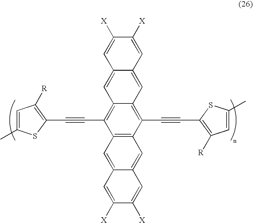
- a class of ethynylene acene polymers are represented by the following formulas/structures wherein R is an alkyl of butyl, pentyl, hexyl, heptyl, octyl, nonyl, decyl, undecyl, dodecyl, tridecyl, tetradecyl, pentadecyl, hexadecyl, heptadecyl, octadecyl; an aryl of butylphenyl, pentylphenyl, hexylphenyl, heptylphenyl, octylphenyl, nonylphenyl, decylphenyl, undecylphenyl, dodecylphenyl, tridecylphenyl, tetradecylphenyl, pentadecylphenyl, hexadeccyl
- a specific class of ethynylene acene polymers are represented by the following formulas/structures wherein R is an alkyl of butyl, pentyl, hexyl, heptyl, octyl, nonyl, decyl, undecyl, dodecyl, tridecyl, tetradecyl, pentadecyl, hexadecyl, heptadecyl, octadecyl; an aryl of butylphenyl, pentylphenyl, hexylphenyl, heptylphenyl, octylphenyl, nonylphenyl, decylphenyl, undecylphenyl, dodecylphenyl, tridecylphenyl, tetradecylphenyl, pentadecylphenyl, hexade
- Suitable hydrocarbons are alkyl and alkoxy with, for example, from about 1 to about 30 carbon atoms, from 1 to about 24 carbon atoms, or from 1 to about 10 carbon atoms, while aryl contains, for example, from 6 to about 48 carbon atoms, from 6 to about 36, or from 6 to about 18 carbon atoms.
- Other known suitable hydrocarbons may also be selected including, for example, substituted alkyl, substituted aryl, alkylaryl, and the like.
- heteroatoms are selenium, oxygen, sulfur, and the like. Heteroatom containing groups are as illustrated herein wherein alkyl and alkoxy are as described with regard to Formula (I), and wherein phenyl can be an aryl group.
- R 1 and R 2 may in embodiments also be a hydrogen atom or a halogen, x and x can be from zero to 16; a, b, c, and f can be from zero to 6; d and e can be from 1 to 4; and n can be 25 to about 1,000.
- the ethynylene acene polymers in embodiments are soluble or substantially soluble in common coating solvents, for example, in embodiments they possess a solubility of at least about 0.1 percent by weight, and more specifically, from about 0.5 percent to about 95 percent by weight in such solvents as methylene chloride, 1,2-dichloroethane, tetrahydrofuran, toluene, xylene, mesitylene, chlorobenzene, dichlorobenzene, and the like.
- the ethynylene acene polymers of the present disclosure in embodiments when fabricated as semiconductor channel layers in TFT devices may provide a stable conductivity of, for example, from about 10 ⁇ 9 S/cm to about 10 ⁇ 4 S/cm, and more specifically, from about 10 ⁇ 8 S/cm to about 10 ⁇ 5 S/cm as determined by conventional four-probe conductivity measurements.
- ethynylene acene polymers when fabricated from solutions as thin films are, for example, from about 10 nanometers to about 500 nanometers or from about 100 to about 350 nanometers in thickness, are more stable in ambient conditions than similar devices fabricated from a number of know semiconductive materials.
- the devices fabricated from the ethynylene acene polymers in embodiments of the present disclosure can provide higher current on/off ratios, and their performance characteristics do not substantially change as rapidly as that of poly(3-alkylthiophene-2,5-diyl) when no rigorous procedural precautions have been taken to exclude ambient oxygen during material preparation, device fabrication, and evaluation.
- ethynylene acene polymers stability of the present disclosure in embodiments against oxidative doping, particularly for low cost device manufacturing, do not usually have to be usually processed in an inert atmosphere and the processes thereof are, therefore, simpler and more cost effective, and the fabrication thereof can be applied to large scale production processes.
- a process for the preparation of the ethynylene acene polymers is represented by reaction Scheme 1.
- 2-bromo-5-chloro-3-dodecylthiophene can be prepared by brominating 3-dodecylthiophene with 1 molar equivalent of N-bromosuccinimide (NBS) in N,N-dimethylformamide (DMF) at room temperature (rt) (as used herein, “room temperature” refers, for example, to a temperature ranging from about 22° C. to about 25° C.).
- 5-chloro-3-dodecyl-2-(trimethylsilyl)ethynylthiophene is stirred in a mixture of methanol/dichloromethane (1/2, v/v) in the presence of 10 percent mol of potassium carbonate at room temperature for a suitable time like 16 hours to produce 5-chloro-3-dodecyl-2-ethynylthiophene.
- 5-Chloro-3-dodecyl-2-ethynylthiophene is then reacted with isopropylmagnesium chloride, and then with anthraquinone or 6,13-pentacenequinone at 50° C. in tetrahydrofuran (THF) under argon, followed by reduction with tin (II) chloride (SnCl 2 ) solution in 10 percent HCl at elevated temperatures like 50° C.
- the resultant 9,10-bis(5-chloro-3-dodecylthienylethynyl)anthracene (M1) or 6,13-bis(5-chloro-3-dodecylthienylethynyl) pentacene (M2) is polymerized using zinc in the presence of nickel (II) chloride (NiCl 2 ), 2,2′-dipyridil, triphenylphosphine (PPh 3 ) in N,N-dimethylacetamide (DMAc) at elevated temperatures like 80° C. for a suitable time like 48 hours.
- Poly(9,10-bis(3-dodecylthienylethynyl)anthracene (6a) and poly(6,13-bis(3-dodecylthienylethynyl) pentacene (22a) are thus obtained.
- an electronic device containing the ethynylene acene polymers illustrated herein; a device which is a thin film transistor comprised of a substrate, a gate electrode, a gate dielectric layer, a source electrode and a drain electrode, and in contact with the source/drain electrodes and the gate dielectric layer, a semiconductor layer comprised of the ethynylene acene polymers illustrated herein; an electronic device, such as a thin film transistor, comprising a polymer of Formula (I) wherein at least one of R 1 and R 2 is a suitable hydrocarbon, such as alkyl, aryl, and the like; hydrogen, a heteroatom containing group, a halogen and the like; Ar and Ar′ represent an aromatic moiety; x, y, a, b, c, d, e, f, and g represent the number of groups or rings, respectively; and n represents the number of repeating units; a thin film transistor comprised of Formula (I) wherein at least one
- FIG. 1 there is schematically illustrated a TFT configuration 10 comprised of a substrate 16 , in contact therewith a metal contact 18 (gate electrode), and a layer of an insulating dielectric layer 14 with the gate electrode having a portion thereof or the entire gate in contact with the dielectric layer 14 , on top of which layer 14 two metal contacts, 20 and 22 (source and drain electrodes), are deposited.
- a metal contact 18 gate electrode
- a layer of an insulating dielectric layer 14 with the gate electrode having a portion thereof or the entire gate in contact with the dielectric layer 14 , on top of which layer 14 two metal contacts, 20 and 22 (source and drain electrodes), are deposited.
- ethynylene acene polymer poly(9,10-bis(3-dodecylthienylethynyl)anthracene) (6a) or poly(6,13-bis(3-dodecylthienylethynyl)pentacene) (22a) layer 12 .
- the gate electrode can be included in the substrate, in the dielectric layer, and the like throughout.
- FIG. 2 schematically illustrates another TFT configuration 30 comprised of a substrate 36 , a gate electrode 38 , a source electrode 40 , and a drain electrode 42 , an insulating dielectric layer 34 , and the ethynylene acene polymer poly(9,10-bis(3-dodecylthienylethynyl)anthracene) (6a) semiconductor layer 32 .
- FIG. 3 schematically illustrates a further TFT configuration 50 comprised of a heavily n-doped silicon wafer 56 , which can act as a gate electrode, a thermally grown silicon oxide dielectric layer 54 , the ethynylene acene polymer poly(9,10-bis(3-dodecylthienylethynyl)anthracene) (6a) semiconductor layer 52 , on top of which are deposited a source electrode 60 and a drain electrode 62 ; and a gate electrode contact 64 .
- a heavily n-doped silicon wafer 56 which can act as a gate electrode
- a thermally grown silicon oxide dielectric layer 54 the ethynylene acene polymer poly(9,10-bis(3-dodecylthienylethynyl)anthracene) (6a) semiconductor layer 52 , on top of which are deposited a source electrode 60 and a drain electrode 62 ; and a gate electrode
- FIG. 4 schematically illustrates a TFT configuration 70 comprised of substrate 76 , a gate electrode 78 , a source electrode 80 , a drain electrode 82 , the ethynylene acene polymer poly(9,10-bis(3-dodecylthienylethynyl)anthracene) (6a) semiconductor layer 72 , and an insulating dielectric layer 74 .
- TFT devices are envisioned, reference for example known TFT devices.
- an optional protecting layer may be incorporated on top of each of the transistor configurations of FIGS. 1, 2 , 3 and 4 .
- the insulating dielectric layer 74 may also function as a protecting layer.
- the substrate layer may generally be a silicon material inclusive of various appropriate forms of silicon, a glass plate, a plastic film or a sheet, and the like depending on the intended applications.
- a plastic substrate such as for example polyester, polycarbonate, polyimide sheets, and the like, may be selected.
- the thickness of the substrate may be, for example, from about 10 micrometers to over 10 millimeters with a specific thickness being from about 50 to about 100 micrometers, especially for a flexible plastic substrate and from about 1 to about 10 millimeters for a rigid substrate, such as glass or silicon.
- the insulating dielectric layer which can separate the gate electrode from the source and drain electrodes, and in contact with the semiconductor layer, can generally be an inorganic material film, an organic polymer film, or an organic-inorganic composite film.
- the thickness of the dielectric layer is, for example, from about 10 nanometers to about 1 micrometer with a more specific thickness being about 100 nanometers to about 500 nanometers.
- Illustrative examples of inorganic materials suitable as the dielectric layer include silicon oxide, silicon nitride, aluminum oxide, barium titanate, barium zirconate titanate, and the like; illustrative examples of organic polymers for the dielectric layer include polyesters, polycarbonates, poly(vinyl phenol), polyimides, polystyrene, poly(methacrylate)s, poly(acrylate)s, epoxy resin, and the like; and illustrative examples of inorganic-organic composite materials include nanosized metal oxide particles dispersed in polymers such as polyester, polyimide, epoxy resin and the like.
- the insulating dielectric layer is generally of a thickness of from about 50 nanometers to about 500 nanometers depending on the dielectric constant of the dielectric material used. More specifically, the dielectric material has a dielectric constant of, for example, at least about 3, thus a suitable dielectric thickness of about 300 nanometers can provide a desirable capacitance, for example, of about 10 ⁇ 9 to about 10 ⁇ 7 F/cm 2 .
- the active semiconductor layer comprised of the ethynylene acene polymers illustrated herein, and wherein the thickness of this layer is generally, for example, about 10 nanometers to about 1 micrometer, or about 40 to about 100 nanometers.
- This layer can generally be fabricated by solution processes such as spin coating, casting, screen, stamp, or jet printing of a solution of the ethynylene acene polymers of the present disclosure.
- the gate electrode can be a thin metal film, a conducting polymer film, a conducting film generated from a conducting ink or paste, or the substrate itself (for example heavily doped silicon).
- gate electrode materials include, but are not limited to aluminum, gold, chromium, indium tin oxide, conducting polymers, such as polystyrene sulfonate-doped poly(3,4-ethylenedioxythiophene) (PSS/PEDOT), a conducting ink/paste comprised of carbon black/graphite or colloidal silver dispersion contained in a polymer binder, such as Electrodag available from Acheson Colloids Company, and silver filled electrically conductive thermoplastic ink available from Noelle Industries, and the like.
- the gate layer can be prepared by vacuum evaporation, sputtering of metals or conductive metal oxides, coating from conducting polymer solutions or conducting inks or dispersions by spin coating, casting or printing.
- the thickness of the gate electrode layer is, for example, from about 10 nanometers to about 10 micrometers, and a specific thickness is, for example, from about 10 to about 200 nanometers for metal films and about 1 to about 10 micrometers for polymer conductors.
- the source and drain electrode layer can be fabricated from materials which provide a low resistance ohmic contact to the semiconductor layer.
- Typical materials suitable for use as source and drain electrodes include those of the gate electrode materials such as gold, nickel, aluminum, platinum, conducting polymers, and conducting inks.
- Typical thickness of this layer is, for example, from about 40 nanometers to about 1 micrometer with the more specific thickness being about 100 to about 400 nanometers.
- the TFT devices contain a semiconductor channel with a width W and length L.
- the semiconductor channel width may be, for example, from about 10 micrometers to about 5 millimeters with a specific channel width being about 100 micrometers to about 1 millimeter.
- the semiconductor channel length may be, for example, from about 1 micrometer to about 1 millimeter with a more specific channel length being from about 5 micrometers to about 100 micrometers.
- the source electrode is grounded and a bias voltage of generally, for example, about 0 volt to about ⁇ 85 volts is applied to the drain electrode to collect the charge carriers transported across the semiconductor channel when a voltage of generally about +10 volts to about ⁇ 80 volts is applied to the gate electrode.
- the ethynyl groups function primarily to minimize or avoid instability because of exposure to oxygen and thus increase the oxidative stability of the ethynylene acene polymers in solution under ambient conditions, and the substituents or groups permit the solubility of these compounds in common solvents, such as ethylene chloride.
Abstract

wherein at least one of R1 and R2 is a suitable hydrocarbon, hydrogen, a heteroatom containing group, or a halogen; Ar and Ar′ represent an aromatic moiety; x, y, a, b, c, d, e, f, and g represent the number of groups or rings, respectively; and n represents the number of repeating units.
Description
- The electronic devices and certain components thereof were supported by a United States Government Cooperative Agreement No. 70NANBOH3033 awarded by the National Institute of Standards and Technology (NIST). The United States Government has certain rights relating to the devices and certain semiconductor components illustrated hereinafter.
- U.S. application No. (not yet assigned) (Attorney Docket No. 20050024-US-NP), filed concurrently herewith, on Functionalized Heteroacenes and Electronic Devices Generated Therefrom, by Yuning Li et al.
- U.S. application No. (not yet assigned) (Attorney Docket No. 20050024Q-US-NP), filed concurrently herewith, on Functionalized Heteroacenes, by Yuning Li et al.
- U.S. application No. (not yet assigned) (Attorney Docket No. 20050471-US-NP), filed concurrently herewith, on Polyacenes and Electronic Devices Generated Therefrom, by Yuning Li et al.
- U.S. application No. (not yet assigned) (Attorney Docket No. 20050472-US-NP), filed concurrently herewith, on Heteroacene Polymers and Electronic Devices Generated Therefrom, by Yuning Li et al.
- U.S. application No. (not yet assigned) (Attorney Docket No. 20050473Q-US-NP), filed concurrently herewith, on Ethynylene Acene Polymers, by Yuning Li et al.
- U.S. application No. (not yet assigned) (Attorney Docket No. 20050474-US-NP), filed concurrently herewith, on Poly[bis(ethynyl)heteroacenes] and Electronic Devices Generated Therefrom, by Yuning Li et al.
- U.S. application No. (not yet assigned) (Attorney Docket No. 20050539-US-NP), filed concurrently herewith, on Semiconductors and Electronic Devices Generated Therefrom, by Yiliang Wu et al.
- U.S. application No. (not yet assigned) (Attorney Docket No. 20050539Q-US-NP), filed concurrently herewith, on Semiconductor Polymers, by Yiliang Wu et al.
- U.S. application No. (not yet assigned) (Attorney Docket No. 20050540-US-NP), filed concurrently herewith, on Polydiazaacenes and Electronic Devices Generated Therefrom, by Yiliang Wu et al.
- U.S. application No. (not yet assigned) (Attorney Docket No. 20050540Q-US-NP), filed concurrently herewith, on Polydiazaacenes, by Yiliang Wu et al.
- U.S. application No. (not yet assigned) (Attorney Docket No. 20050707-US-NP), filed concurrently herewith, on Poly(alkynylthiophene)s and Electronic Devices Generated Therefrom, by Beng S. Ong et al.
- U.S. application No. (not yet assigned) (Attorney Docket No. 20050707Q-US-NP), filed concurrently herewith, on Poly(alkynylthiophene)s, by Beng S. Ong et al.
- U.S. application No. (not yet assigned) (Attorney Docket No. 20050711-US-NP), filed concurrently herewith, on Linked Arylamine Polymers and Electronic Devices Generated Therefrom, by Yuning Li et al.
- U.S. application No. (not yet assigned) (Attorney Docket No. 20050711Q-US-NP), filed concurrently herewith, on Linked Arylamine Polymers, by Yuning Li et al.
- Illustrated in U.S. application Ser. No. 11/011,678 (Attorney Docket No. A3571-US-NP) filed Dec. 14, 2004 relating to indolocarbazole moieties and thin film transistor devices thereof.
- Illustrated in U.S. application Ser. No. 11/167,512 (Attorney Docket No. A3571-US-CIP) filed Jun. 27, 2005 relating to indolocarbazole moieties and thin film transistor devices thereof.
- Illustrated in U.S. Pat. No. 6,770,904 and copending application U.S. application Ser. No. 10/922,662, Publication No. 20050017311 (Attorney Docket No. A1332-US-CIP), are electronic devices, such as thin film transistors containing semiconductor layers of, for example, polythiophenes.
- The disclosure of each of the above cross referenced applications and patent is totally incorporated herein by reference. In aspects of the present disclosure, there may be selected the appropriate substituents, such as a suitable hydrocarbon, a heteroatom containing group, hydrogen, halogen, CN, NO2, rings, number of repeating polymer units, number of groups, and the like as illustrated in the copending applications.
- The appropriate components, processes thereof and uses thereof illustrated in these copending applications and patent may be selected for the present invention in embodiments thereof.
- The present disclosure is generally directed to novel polymers, such as ethynylene acene polymers, and uses thereof. More specifically, the present disclosure in embodiments is directed to ethynylene acene polymers selected as solution processable and substantially stable channel semiconductors in organic electronic devices, such as thin film transistors.
- There is desired electronic devices, such as thin film transistors, TFTs, fabricated with ethynylene acene polymers, with excellent solvent solubility, which can be solution processable; and devices thereof with mechanical durability and structural flexibility, desirable for fabricating flexible TFTs on plastic substrates. Flexible TFTs would enable the design of electronic devices which usually possesses structural flexibility and mechanical durability characteristics. The use of plastic substrates together with the ethynylene acene polymers can transform the traditionally rigid silicon TFT into a mechanically more durable and structurally flexible TFT design. This can be of particular value to large area devices, such as large-area image sensors, electronic paper and other display media. Also, the selection of ethynylene acene polymer TFTs for integrated circuit logic elements for low end microelectronics, such as smart cards, radio frequency identification (RFID) tags, and memory/storage devices, may enhance their mechanical durability, and thus increase their useful life span.
- A number of semiconductor materials are not, it is believed, that stable when exposed to air as they become oxidatively doped by ambient oxygen, resulting in increased conductivity. The result is large off-current and thus low current on/off ratio for the devices fabricated from these materials. Accordingly, with many of these materials, rigorous precautions are usually undertaken during materials processing and device fabrication to exclude environmental oxygen to avoid or minimize oxidative doping. These precautionary measures increase the cost of manufacturing therefore offsetting the appeal of certain semiconductor TFTs as an economical alternative to amorphous silicon technology, particularly for large area devices. These and other disadvantages are avoided or minimized in embodiments of the present disclosure.
- Heteroacenes and acenes like pentacene are known to possess acceptable high field effect mobility when used as channel semiconductors in TFTs. However, these materials are rapidly oxidized by, for example, atmospheric oxygen under light and such compounds are not considered processable at ambient conditions. Furthermore, heteroacenes when selected for TFTs have poor thin film formation characteristics and are insoluble or have minimal solubility in a number of commonly known solvents, rendering these compounds substantially nonsolution processing; accordingly, such materials have been processed by vacuum deposition methods that result in high production costs, eliminated or minimized with the TFTs generated with the ethynylene acene polymers illustrated herein.
- A number of organic semiconductor materials has been described for use in field effect TFTs, which materials include organic small molecules, such as pentacene, see for example, D. J. Gundlach et al., “Pentacene organic thin film transistors—molecular ordering and mobility”, IEEE Electron Device Lett., Vol. 18, p. 87 (1997); oligomers, such as sexithiophenes or their variants, see for example, reference F. Garnier et al., “Molecular engineering of organic semiconductors: Design of self-assembly properties in conjugated thiophene oligomers”, J. Amer. Chem. Soc., Vol. 115, p. 8716 (1993), and poly(3-alkylthiophene), see for example, reference Z. Bao et al., “Soluble and processable regioregular poly(3-hexylthiophene) for field-effect thin film transistor application with high mobility”, Appl. Phys. Lett. Vol. 69, p 4108 (1996). Although organic material based TFTs generally provide lower performance characteristics than their conventional silicon counterparts, such as silicon crystals or polysilicon TFTs, they may nonetheless be sufficiently useful for applications in areas where high mobility is not of importance. These include large area devices, such as image sensors, active matrix liquid crystal displays and low end microelectronics, such as smart cards and RFID tags. Also, vacuum deposition of the semiconductive layer is selected for a number of TFTs primarily because they are either insoluble or their solution processing by spin coating, solution casting, or stamp printing does not generally provide uniform thin films.
- TFTs fabricated from ethynylene acene polymers may be functionally and structurally more desirable than conventional silicon technology in that they offer mechanical durability, structural flexibility, and the potential of being able to be incorporated directly onto the active media of the devices, thus enhancing device compactness for transportability. Polymer TFTs, such as those fabricated from regioregular components of, for example, regioregular poly(3-alkylthiophene-2,5-diyl) by solution processes, while offering some mobility, suffer from their propensity towards oxidative doping in air. For practical low cost TFT design, it is therefore of value to have a semiconductor material that is both stable and solution processable, and where its performance is not adversely affected by ambient oxygen, for example, TFTs generated with poly(3-alkylthiophene-2,5-diyl) are sensitive to air. The TFTs fabricated from these materials in ambient conditions generally exhibit high off-current, very low current on/off ratios, and their performance characteristics degrade rapidly.
- Illustrated in Huang, D. H., et al, Chem. Mater. 2004, 16, 1298-1303, are, for example, LEDs and field effect transistors based on certain phenothiaazines like poly(10-(2-ethylhexyl)phenothiaazine).
- Illustrated in Zhu, Y., et al, Macromolecules 2005, 38, 7983-7991, are, for example semiconductors based on phenoxazine conjugated polymers like poly(10-hexylphenoxazine).
- Additional references that may be of interest include U.S. Pat. Nos. 6,150,191; 6,107,117; 5,969,376; 5,619,357, and 5,777,070.
- Illustrated in FIGS. 1 to 4 are various representative embodiments of the present disclosure and wherein ethynylene acene polymers are selected as the channel or semiconductor material in thin film transistor (TFT) configurations.
- It is a feature of the present disclosure to provide semiconductor ethynylene acene polymers, which are useful for microelectronic device applications, such as TFT devices.
- It is another feature of the present disclosure to provide ethynylene acene polymers with a band gap of from about 1.5 eV to about 3 eV as determined from the absorption spectra of thin films thereof, and which ethynylene acene polymers are suitable for use as TFT semiconductor channel layer materials.
- In yet a further feature of the present disclosure there are provided ethynylene acene polymers, which are useful as microelectronic components, and which ethynylene acene polymers possess solubility of, for example, at least about 0.1 percent to about 95 percent by weight in known organic solvents, such as methylene chloride, tetrahydrofuran, toluene, xylene, mesitylene, chlorobenzene, and the like, and thus these components can be economically fabricated by solution processes, such as spin coating, screen printing, stamp printing, dip coating, solution casting, jet printing, and the like.
- Another feature of the present disclosure resides in providing electronic devices, such as TFTs, with an ethynylene acene polymer channel layer, and which layer has a conductivity of from about 10−4 to about 10−9 S/cm (Siemens/centimeter).
- Also, in yet another feature of the present disclosure there are provided novel ethynylene acene polymers and devices thereof, and which devices exhibit, it is believed, enhanced resistance to the adverse effects of oxygen, that is, these devices exhibit relatively high current on/off ratios, and their performance does not substantially degrade as rapidly as similar devices fabricated with regioregular poly(3-alkylthiophene-3,5-diyl).
- Additionally, in a further feature of the present disclosure there is provided a class of novel ethynylene acene polymers with unique structural features which enable molecular self-alignment under appropriate processing conditions, and which structural features also enhance the stability of device performance. Proper molecular alignment can permit higher molecular structural order in thin films, which can be important to efficient charge carrier transport, thus resulting in higher electrical performance.
- There are disclosed in embodiments, ethynylene acene polymers and electronic devices thereof. More specifically, the present disclosure relates to ethynylene acene polymers illustrated by or encompassed by Formula (I) and a semiconductive material containing an ethynylene acene polymer of Formula (I)

wherein each R1 and R2 is independently a suitable hydrocarbon, such as alkyl with 1 to about 30 carbon atoms like methyl, ethyl, butyl, pentyl, hexyl, heptyl, octyl, nonyl, decyl, undecyl, dodecyl, tridecyl, tetradecyl, pentadecyl, hexadecyl, heptadecyl, octadecyl, nonadecyl, or eicosanyl; aryl with about 6 to about 48 carbon atoms, such as phenyl, tolyl, ethylphenyl, propylphenyl, butylphenyl, pentylphenyl, hexylphenyl, heptylphenyl, octylphenyl, nonylphenyl, decylphenyl, undecylphenyl, dodecylphenyl, tridecylphenyl, tetradecylphenyl, pentadecylphenyl, hexadecylphenyl, heptadecylphenyl, or octadecylphenyl; a heteroatom containing group with zero to about 36 carbon atoms, such as nitro (NO2), cyano (CN); dialkylamino, such as dimethylamino, diethylamino, dipropylamino, dibutylamino; diarylamino such as diphenylamino, ditolylamino, di(ethylphenyl)amino, di(propylphenyl)amino, and di(butylphenyl)amino; alkoxy with from about 1 to about 30 carbon atoms, such as methoxy, ethoxy, propyloxy, butyloxy, pentyloxy, hexyloxy, heptyloxy, ocyloxy, nonyloxy, decyloxy, undecyloxy, dodecyloxy, tridecyloxy, tetradecyloxy, pentadecyloxy, hexadecyloxy, heptadecyloxy, octadecyloxy, nonadecyloxy, or eicosanyloxy; trialkylsilyls such as trimethylsilyl, triethylsilyl, tripropylsilyl, tributylsilyl, tripentylsilyl, and trihexylsilyl; triarylsilyls, such as triphenylsilyl, tritolylsilyl, tri(ethylphenyl)silyl, tri(propylphenyl)silyl, and tri(butylphenyl)silyl, or a halogen such as fluorine, chlorine, bromine, and iodine; Ar and Ar′ each independently represents an aromatic moiety; x, y, a, b, c, d, e, f, and g represent the number of groups or rings; and n represents the number of repeating units; Ar and Ar′ are aromatic moieties, for example, independently selected from the group consisting of the following structural units which are optionally substituted; and wherein X is selected from the group consisting of C(R′R″), O, S, Se, NR, and Si(R′R″), and wherein R, R′, and R″ are independently selected from the group consisting of hydrogen, a suitable hydrocarbon group, such as alkyl with 1 to about 24 carbon atoms, aryl with from about 6 to about 36 carbon atoms; and Y is a carbon atom or a nitrogen atom
x and y each represent the number of groups and can be from zero to about 12; a and b each represent the number of fused ring moieties and can be, for example, from zero to about 6, and more specifically, wherein each a and b are from about zero to about 5; c represents the number of the aromatic units, Ar, and can be, for example, from zero to about 10, and more specifically, from zero to about 6; e represents the number of acene moieties, and can be, for example, from about 1 to about 10, and more specifically, from about 1 to about 4; d and f each independently represent an alkynyl like ethynyl groups (triple bond) and can be from zero to about 4, and more specifically, from zero to about 2; g represents the number of the aromatic units, Ar′, and can be, for example, from zero to about 10, and more specifically, from zero to about 6; n represents the number of repeating units, such as, for example, n is a number of from about 2 to about 5,000, from about 2 to about 1,000, or from about 5 to about 500. The sum of a and b can be, for example, from 1 to about 6, and more specifically, from about 2 to about 4. The sum of c and g can be, for example, from zero to about 20, and more specifically, from zero to about 10; the sum of d and f can be, for example, from 1 to about 4, and more specifically, from 1 to 2. - In embodiments, a class of ethynylene acene polymers are represented by the following formulas/structures


wherein R is an alkyl of butyl, pentyl, hexyl, heptyl, octyl, nonyl, decyl, undecyl, dodecyl, tridecyl, tetradecyl, pentadecyl, hexadecyl, heptadecyl, octadecyl; an aryl of butylphenyl, pentylphenyl, hexylphenyl, heptylphenyl, octylphenyl, nonylphenyl, decylphenyl, undecylphenyl, dodecylphenyl, tridecylphenyl, tetradecylphenyl, pentadecylphenyl, hexadecylphenyl, heptadecylphenyl, or octadecylphenyl; an alkoxy of butyloxy, pentyloxy, hexyloxy, heptyloxy, ocyloxy, nonyloxy, decyloxy, undecyloxy, dodecyloxy, tridecyloxy, tetradecyloxy, pentadecyloxy, hexadecyloxy, heptadecyloxy, octadecyloxy, nonadecyloxy, or eicosanyloxy; and wherein X is methyl, CF3, NO2, CN, F, or Cl; and wherein n is the number of repeating units in the polymer of from about 2 to about 1,000. - In embodiments, a specific class of ethynylene acene polymers are represented by the following formulas/structures

wherein R is an alkyl of butyl, pentyl, hexyl, heptyl, octyl, nonyl, decyl, undecyl, dodecyl, tridecyl, tetradecyl, pentadecyl, hexadecyl, heptadecyl, octadecyl; an aryl of butylphenyl, pentylphenyl, hexylphenyl, heptylphenyl, octylphenyl, nonylphenyl, decylphenyl, undecylphenyl, dodecylphenyl, tridecylphenyl, tetradecylphenyl, pentadecylphenyl, hexadecylphenyl, heptadecylphenyl, or octadecylphenyl; an alkoxy of butyloxy, pentyloxy, hexyloxy, heptyloxy, ocyloxy, nonyloxy, decyloxy, undecyloxy, dodecyloxy, tridecyloxy, tetradecyloxy, pentadecyloxy, hexadecyloxy, heptadecyloxy, octadecyloxy, nonadecyloxy, or eicosanyloxy; and wherein n is the number of repeating units in the polymer of from about 2 to about 100. - Suitable hydrocarbons are alkyl and alkoxy with, for example, from about 1 to about 30 carbon atoms, from 1 to about 24 carbon atoms, or from 1 to about 10 carbon atoms, while aryl contains, for example, from 6 to about 48 carbon atoms, from 6 to about 36, or from 6 to about 18 carbon atoms. Other known suitable hydrocarbons may also be selected including, for example, substituted alkyl, substituted aryl, alkylaryl, and the like. Examples of heteroatoms are selenium, oxygen, sulfur, and the like. Heteroatom containing groups are as illustrated herein wherein alkyl and alkoxy are as described with regard to Formula (I), and wherein phenyl can be an aryl group. R1 and R2 may in embodiments also be a hydrogen atom or a halogen, x and x can be from zero to 16; a, b, c, and f can be from zero to 6; d and e can be from 1 to 4; and n can be 25 to about 1,000.
- The ethynylene acene polymers in embodiments are soluble or substantially soluble in common coating solvents, for example, in embodiments they possess a solubility of at least about 0.1 percent by weight, and more specifically, from about 0.5 percent to about 95 percent by weight in such solvents as methylene chloride, 1,2-dichloroethane, tetrahydrofuran, toluene, xylene, mesitylene, chlorobenzene, dichlorobenzene, and the like. Moreover, the ethynylene acene polymers of the present disclosure in embodiments when fabricated as semiconductor channel layers in TFT devices may provide a stable conductivity of, for example, from about 10−9 S/cm to about 10−4 S/cm, and more specifically, from about 10−8 S/cm to about 10−5 S/cm as determined by conventional four-probe conductivity measurements.
- It is believed that the ethynylene acene polymers, when fabricated from solutions as thin films are, for example, from about 10 nanometers to about 500 nanometers or from about 100 to about 350 nanometers in thickness, are more stable in ambient conditions than similar devices fabricated from a number of know semiconductive materials. When unprotected, electronic devices containing the aforementioned ethynylene acene polymer materials are generally stable for a number of weeks rather than days or hours as is the situation with poly(3-alkylthiophene-2,5-diyl) after exposure to ambient oxygen, thus the devices fabricated from the ethynylene acene polymers in embodiments of the present disclosure can provide higher current on/off ratios, and their performance characteristics do not substantially change as rapidly as that of poly(3-alkylthiophene-2,5-diyl) when no rigorous procedural precautions have been taken to exclude ambient oxygen during material preparation, device fabrication, and evaluation. The ethynylene acene polymers stability of the present disclosure in embodiments against oxidative doping, particularly for low cost device manufacturing, do not usually have to be usually processed in an inert atmosphere and the processes thereof are, therefore, simpler and more cost effective, and the fabrication thereof can be applied to large scale production processes.
- A process for the preparation of the ethynylene acene polymers is represented by reaction Scheme 1.

First, 2-bromo-5-chloro-3-dodecylthiophene can be prepared by brominating 3-dodecylthiophene with 1 molar equivalent of N-bromosuccinimide (NBS) in N,N-dimethylformamide (DMF) at room temperature (rt) (as used herein, “room temperature” refers, for example, to a temperature ranging from about 22° C. to about 25° C.). Next, the chlorination of 2-bromo-3-dodecylthiophene with 1 molar equivalent of N-chlorosuccinimide (NCS) at room temperature generates 2-bromo-5-chloro-3-dodecylthiophene. Subsequently, 2-bromo-5-chloro-3-dodecylthiophene is reacted with a trimethylsilylacetylene in the presence of dichlorobis(triphenylphosphine) palladium (11) (Pd(PPh3)2Cl2) and copper(I) iodide (CuI) in triethylamine (Et3N) at elevated temperatures, such as 50° C. for a suitable time like 24 hours, and 80° C. for 3 hours under argon to form 5-chloro-3-dodecyl-2-(trimethylsilyl)ethynylthiophene. 5-Chloro-3-dodecyl-2-(trimethylsilyl)ethynylthiophene is stirred in a mixture of methanol/dichloromethane (1/2, v/v) in the presence of 10 percent mol of potassium carbonate at room temperature for a suitable time like 16 hours to produce 5-chloro-3-dodecyl-2-ethynylthiophene. 5-Chloro-3-dodecyl-2-ethynylthiophene is then reacted with isopropylmagnesium chloride, and then with anthraquinone or 6,13-pentacenequinone at 50° C. in tetrahydrofuran (THF) under argon, followed by reduction with tin (II) chloride (SnCl2) solution in 10 percent HCl at elevated temperatures like 50° C. The resultant 9,10-bis(5-chloro-3-dodecylthienylethynyl)anthracene (M1) or 6,13-bis(5-chloro-3-dodecylthienylethynyl) pentacene (M2) is polymerized using zinc in the presence of nickel (II) chloride (NiCl2), 2,2′-dipyridil, triphenylphosphine (PPh3) in N,N-dimethylacetamide (DMAc) at elevated temperatures like 80° C. for a suitable time like 48 hours. Poly(9,10-bis(3-dodecylthienylethynyl)anthracene (6a) and poly(6,13-bis(3-dodecylthienylethynyl) pentacene (22a) are thus obtained. - Aspects of the present disclosure relate to an electronic device containing the ethynylene acene polymers illustrated herein; a device which is a thin film transistor comprised of a substrate, a gate electrode, a gate dielectric layer, a source electrode and a drain electrode, and in contact with the source/drain electrodes and the gate dielectric layer, a semiconductor layer comprised of the ethynylene acene polymers illustrated herein; an electronic device, such as a thin film transistor, comprising a polymer of Formula (I)

wherein at least one of R1 and R2 is a suitable hydrocarbon, such as alkyl, aryl, and the like; hydrogen, a heteroatom containing group, a halogen and the like; Ar and Ar′ represent an aromatic moiety; x, y, a, b, c, d, e, f, and g represent the number of groups or rings, respectively; and n represents the number of repeating units; a thin film transistor comprised of a substrate, a gate electrode, a gate dielectric layer, a source electrode and a drain electrode, and in contact with the source/drain electrodes and the gate dielectric layer a semiconductor layer comprised of an ethynylene acene polymer of the formula
wherein at least one of R1 and R2 is a hydrocarbon, such as alkyl, aryl, substituted alkyl, substituted aryl, alkoxy, substituted alkoxy, and the like, hydrogen, a heteroatom containing group, or a halogen; Ar and Ar′ represent an aromatic moiety; x, y, a, b, c, d, e, f, and g represent the number of groups; and n represents the number of repeating units; a TFT device wherein the substrate is a plastic sheet of a polyester, a polycarbonate, or a polyimide; the gate source and drain electrodes are each independently comprised of gold, nickel, aluminum, platinum, indium titanium oxide, or a conductive polymer, and the gate dielectric is a dielectric layer comprised of silicon nitride or silicon oxide; a TFT device wherein the substrate is glass or a plastic sheet; said gate, source and drain electrodes are each comprised of gold, and the gate dielectric layer is comprised of the organic polymer poly(methacrylate), or poly(vinyl phenol); a device wherein the ethynylene acene polymer layer is formed by solution processes of spin coating, stamp printing, screen printing, or jet printing; a device wherein the gate, source and drain electrodes, the gate dielectric, and semiconductor layers are formed by solution processes of spin coating, solution casting, stamp printing, screen printing, or jet printing; and a TFT device wherein the substrate is a plastic sheet of a polyester, a polycarbonate, or a polyimide, and the gate, source and drain electrodes are fabricated from the organic conductive polymer polystyrene sulfonate-doped poly(3,4-ethylene dioxythiophene), or from a conductive ink/paste compound of a colloidal dispersion of silver in a polymer binder, and the gate dielectric layer is organic polymer or inorganic oxide particle-polymer composite; device or devices include electronic devices, such as TFTs. - In
FIG. 1 there is schematically illustrated aTFT configuration 10 comprised of asubstrate 16, in contact therewith a metal contact 18 (gate electrode), and a layer of an insulatingdielectric layer 14 with the gate electrode having a portion thereof or the entire gate in contact with thedielectric layer 14, on top of whichlayer 14 two metal contacts, 20 and 22 (source and drain electrodes), are deposited. Over and between themetal contacts layer 12. The gate electrode can be included in the substrate, in the dielectric layer, and the like throughout. -
FIG. 2 schematically illustrates anotherTFT configuration 30 comprised of asubstrate 36, agate electrode 38, asource electrode 40, and adrain electrode 42, an insulatingdielectric layer 34, and the ethynylene acene polymer poly(9,10-bis(3-dodecylthienylethynyl)anthracene) (6a)semiconductor layer 32. -
FIG. 3 schematically illustrates afurther TFT configuration 50 comprised of a heavily n-dopedsilicon wafer 56, which can act as a gate electrode, a thermally grown siliconoxide dielectric layer 54, the ethynylene acene polymer poly(9,10-bis(3-dodecylthienylethynyl)anthracene) (6a)semiconductor layer 52, on top of which are deposited asource electrode 60 and adrain electrode 62; and agate electrode contact 64. -
FIG. 4 schematically illustrates aTFT configuration 70 comprised ofsubstrate 76, agate electrode 78, asource electrode 80, adrain electrode 82, the ethynylene acene polymer poly(9,10-bis(3-dodecylthienylethynyl)anthracene) (6a)semiconductor layer 72, and an insulatingdielectric layer 74. - Also, other devices not disclosed, especially TFT devices, are envisioned, reference for example known TFT devices.
- In embodiments of the present disclosure, an optional protecting layer may be incorporated on top of each of the transistor configurations of
FIGS. 1, 2 , 3 and 4. For the TFT configuration ofFIG. 4 , the insulatingdielectric layer 74 may also function as a protecting layer. - In embodiments and with further reference to the present disclosure and the Figures, the substrate layer may generally be a silicon material inclusive of various appropriate forms of silicon, a glass plate, a plastic film or a sheet, and the like depending on the intended applications. For structurally flexible devices, a plastic substrate, such as for example polyester, polycarbonate, polyimide sheets, and the like, may be selected. The thickness of the substrate may be, for example, from about 10 micrometers to over 10 millimeters with a specific thickness being from about 50 to about 100 micrometers, especially for a flexible plastic substrate and from about 1 to about 10 millimeters for a rigid substrate, such as glass or silicon.
- The insulating dielectric layer, which can separate the gate electrode from the source and drain electrodes, and in contact with the semiconductor layer, can generally be an inorganic material film, an organic polymer film, or an organic-inorganic composite film. The thickness of the dielectric layer is, for example, from about 10 nanometers to about 1 micrometer with a more specific thickness being about 100 nanometers to about 500 nanometers. Illustrative examples of inorganic materials suitable as the dielectric layer include silicon oxide, silicon nitride, aluminum oxide, barium titanate, barium zirconate titanate, and the like; illustrative examples of organic polymers for the dielectric layer include polyesters, polycarbonates, poly(vinyl phenol), polyimides, polystyrene, poly(methacrylate)s, poly(acrylate)s, epoxy resin, and the like; and illustrative examples of inorganic-organic composite materials include nanosized metal oxide particles dispersed in polymers such as polyester, polyimide, epoxy resin and the like. The insulating dielectric layer is generally of a thickness of from about 50 nanometers to about 500 nanometers depending on the dielectric constant of the dielectric material used. More specifically, the dielectric material has a dielectric constant of, for example, at least about 3, thus a suitable dielectric thickness of about 300 nanometers can provide a desirable capacitance, for example, of about 10−9 to about 10−7 F/cm2.
- Situated, for example, between and in contact with the dielectric layer and the source/drain electrodes is the active semiconductor layer comprised of the ethynylene acene polymers illustrated herein, and wherein the thickness of this layer is generally, for example, about 10 nanometers to about 1 micrometer, or about 40 to about 100 nanometers. This layer can generally be fabricated by solution processes such as spin coating, casting, screen, stamp, or jet printing of a solution of the ethynylene acene polymers of the present disclosure.
- The gate electrode can be a thin metal film, a conducting polymer film, a conducting film generated from a conducting ink or paste, or the substrate itself (for example heavily doped silicon). Examples of gate electrode materials include, but are not limited to aluminum, gold, chromium, indium tin oxide, conducting polymers, such as polystyrene sulfonate-doped poly(3,4-ethylenedioxythiophene) (PSS/PEDOT), a conducting ink/paste comprised of carbon black/graphite or colloidal silver dispersion contained in a polymer binder, such as Electrodag available from Acheson Colloids Company, and silver filled electrically conductive thermoplastic ink available from Noelle Industries, and the like. The gate layer can be prepared by vacuum evaporation, sputtering of metals or conductive metal oxides, coating from conducting polymer solutions or conducting inks or dispersions by spin coating, casting or printing. The thickness of the gate electrode layer is, for example, from about 10 nanometers to about 10 micrometers, and a specific thickness is, for example, from about 10 to about 200 nanometers for metal films and about 1 to about 10 micrometers for polymer conductors.
- The source and drain electrode layer can be fabricated from materials which provide a low resistance ohmic contact to the semiconductor layer. Typical materials suitable for use as source and drain electrodes include those of the gate electrode materials such as gold, nickel, aluminum, platinum, conducting polymers, and conducting inks. Typical thickness of this layer is, for example, from about 40 nanometers to about 1 micrometer with the more specific thickness being about 100 to about 400 nanometers. The TFT devices contain a semiconductor channel with a width W and length L. The semiconductor channel width may be, for example, from about 10 micrometers to about 5 millimeters with a specific channel width being about 100 micrometers to about 1 millimeter. The semiconductor channel length may be, for example, from about 1 micrometer to about 1 millimeter with a more specific channel length being from about 5 micrometers to about 100 micrometers.
- The source electrode is grounded and a bias voltage of generally, for example, about 0 volt to about −85 volts is applied to the drain electrode to collect the charge carriers transported across the semiconductor channel when a voltage of generally about +10 volts to about −80 volts is applied to the gate electrode.
- Other known materials not recited herein for the various components of the TFT devices of the present disclosure can also be selected in embodiments.
- Although not desiring to be limited by theory, it is believed that the ethynyl groups function primarily to minimize or avoid instability because of exposure to oxygen and thus increase the oxidative stability of the ethynylene acene polymers in solution under ambient conditions, and the substituents or groups permit the solubility of these compounds in common solvents, such as ethylene chloride.
- The claims, as originally presented and as they may be amended, encompass variations, alternatives, modifications, improvements, equivalents, and substantial equivalents of the embodiments and teachings disclosed herein, including those that are presently unforeseen or unappreciated, and that, for example, may arise from applicants/patentees and others. Unless specifically recited in a claim, steps or components of claims should not be implied or imported from the specification or any other claims as to any particular order, number, position, size, shape, angle, color, or material.
Claims (33)


Priority Applications (1)
| Application Number | Priority Date | Filing Date | Title |
|---|---|---|---|
| US11/399,169 US7586120B2 (en) | 2006-04-06 | 2006-04-06 | Ethynylene acene polymers and electronic devices generated therefrom |
Applications Claiming Priority (1)
| Application Number | Priority Date | Filing Date | Title |
|---|---|---|---|
| US11/399,169 US7586120B2 (en) | 2006-04-06 | 2006-04-06 | Ethynylene acene polymers and electronic devices generated therefrom |
Publications (2)
| Publication Number | Publication Date |
|---|---|
| US20070235725A1 true US20070235725A1 (en) | 2007-10-11 |
| US7586120B2 US7586120B2 (en) | 2009-09-08 |
Family
ID=38574258
Family Applications (1)
| Application Number | Title | Priority Date | Filing Date |
|---|---|---|---|
| US11/399,169 Active 2027-07-31 US7586120B2 (en) | 2006-04-06 | 2006-04-06 | Ethynylene acene polymers and electronic devices generated therefrom |
Country Status (1)
| Country | Link |
|---|---|
| US (1) | US7586120B2 (en) |
Families Citing this family (1)
| Publication number | Priority date | Publication date | Assignee | Title |
|---|---|---|---|---|
| US20080142793A1 (en) * | 2006-11-10 | 2008-06-19 | Tang Ming L | Organic Semiconductors |
Citations (13)
| Publication number | Priority date | Publication date | Assignee | Title |
|---|---|---|---|---|
| US5055439A (en) * | 1989-12-27 | 1991-10-08 | International Business Machines Corporation | Photoacid generating composition and sensitizer therefor |
| US5619357A (en) * | 1995-06-06 | 1997-04-08 | International Business Machines Corporation | Flat panel display containing black matrix polymer |
| US5777070A (en) * | 1997-10-23 | 1998-07-07 | The Dow Chemical Company | Process for preparing conjugated polymers |
| US5969376A (en) * | 1996-08-23 | 1999-10-19 | Lucent Technologies Inc. | Organic thin film transistor having a phthalocyanine semiconductor layer |
| US6107117A (en) * | 1996-12-20 | 2000-08-22 | Lucent Technologies Inc. | Method of making an organic thin film transistor |
| US6690029B1 (en) * | 2001-08-24 | 2004-02-10 | University Of Kentucky Research Foundation | Substituted pentacenes and electronic devices made with substituted pentacenes |
| US6770904B2 (en) * | 2002-01-11 | 2004-08-03 | Xerox Corporation | Polythiophenes and electronic devices generated therefrom |
| US6795230B1 (en) * | 2003-06-18 | 2004-09-21 | Hewlett-Packard Development Company, L.P. | Self-assembled molecular color switch |
| US20050017311A1 (en) * | 2002-01-11 | 2005-01-27 | Xerox Corporation | Polythiophenes and electronic devices generated therefrom |
| US20060131570A1 (en) * | 2004-11-02 | 2006-06-22 | Hong Meng | Substituted anthracenes and electronic devices containing the substituted anthracenes |
| US20070102696A1 (en) * | 2003-11-28 | 2007-05-10 | Beverley Brown | Organic semiconducting layers |
| US20070146426A1 (en) * | 2005-12-28 | 2007-06-28 | Nelson Brian K | All-inkjet printed thin film transistor |
| US20070176164A1 (en) * | 2004-03-09 | 2007-08-02 | Fumie Sato | -Conjugated aromatic ring-containing compound and organic electroluminescent device |
Family Cites Families (2)
| Publication number | Priority date | Publication date | Assignee | Title |
|---|---|---|---|---|
| JP2002275384A (en) * | 2001-03-16 | 2002-09-25 | Japan Science & Technology Corp | Photoresponsive pigment for laser |
| JP2002363381A (en) * | 2001-06-05 | 2002-12-18 | Sumitomo Bakelite Co Ltd | Flame-retardant epoxy resin composition, semiconductor sealing medium and semiconductor device |
-
2006
- 2006-04-06 US US11/399,169 patent/US7586120B2/en active Active
Patent Citations (14)
| Publication number | Priority date | Publication date | Assignee | Title |
|---|---|---|---|---|
| US5055439A (en) * | 1989-12-27 | 1991-10-08 | International Business Machines Corporation | Photoacid generating composition and sensitizer therefor |
| US5619357A (en) * | 1995-06-06 | 1997-04-08 | International Business Machines Corporation | Flat panel display containing black matrix polymer |
| US5969376A (en) * | 1996-08-23 | 1999-10-19 | Lucent Technologies Inc. | Organic thin film transistor having a phthalocyanine semiconductor layer |
| US6150191A (en) * | 1996-08-23 | 2000-11-21 | Lucent Technologies Inc. | Method of making an organic thin film transistor and article made by the method |
| US6107117A (en) * | 1996-12-20 | 2000-08-22 | Lucent Technologies Inc. | Method of making an organic thin film transistor |
| US5777070A (en) * | 1997-10-23 | 1998-07-07 | The Dow Chemical Company | Process for preparing conjugated polymers |
| US6690029B1 (en) * | 2001-08-24 | 2004-02-10 | University Of Kentucky Research Foundation | Substituted pentacenes and electronic devices made with substituted pentacenes |
| US6770904B2 (en) * | 2002-01-11 | 2004-08-03 | Xerox Corporation | Polythiophenes and electronic devices generated therefrom |
| US20050017311A1 (en) * | 2002-01-11 | 2005-01-27 | Xerox Corporation | Polythiophenes and electronic devices generated therefrom |
| US6795230B1 (en) * | 2003-06-18 | 2004-09-21 | Hewlett-Packard Development Company, L.P. | Self-assembled molecular color switch |
| US20070102696A1 (en) * | 2003-11-28 | 2007-05-10 | Beverley Brown | Organic semiconducting layers |
| US20070176164A1 (en) * | 2004-03-09 | 2007-08-02 | Fumie Sato | -Conjugated aromatic ring-containing compound and organic electroluminescent device |
| US20060131570A1 (en) * | 2004-11-02 | 2006-06-22 | Hong Meng | Substituted anthracenes and electronic devices containing the substituted anthracenes |
| US20070146426A1 (en) * | 2005-12-28 | 2007-06-28 | Nelson Brian K | All-inkjet printed thin film transistor |
Also Published As
| Publication number | Publication date |
|---|---|
| US7586120B2 (en) | 2009-09-08 |
Similar Documents
| Publication | Publication Date | Title |
|---|---|---|
| US7557370B2 (en) | Heteroacene polymers and electronic devices generated therefrom | |
| JP5307349B2 (en) | Functionalized heteroacenes and electronic devices made therefrom | |
| US7994497B2 (en) | Poly[bis(ethynyl)heteroacene]s and electronic devices generated therefrom | |
| US8049205B2 (en) | Poly(alkynylthiophene)s and electronic devices generated therefrom | |
| US7563860B2 (en) | Semiconductors and electronic devices generated therefrom | |
| US7795373B2 (en) | Ethynylene acene polymers | |
| EP1849812B1 (en) | Linked arylamine polymers and electronic devices generated therefrom | |
| US7550760B2 (en) | Polyacenes and electronic devices generated therefrom | |
| US7615607B2 (en) | Semiconductor polymers | |
| US8334391B2 (en) | Functionalized heteroacenes | |
| US7586120B2 (en) | Ethynylene acene polymers and electronic devices generated therefrom | |
| US7847052B2 (en) | Linked arylamine polymers | |
| US7705111B2 (en) | Poly(alkynylthiophene)s | |
| US7517476B2 (en) | Polydiazaacenes | |
| US7517477B2 (en) | Polydiazaacenes and electronic devices generated therefrom |
Legal Events
| Date | Code | Title | Description |
|---|---|---|---|
| AS | Assignment |
Owner name: XEROX CORPORATION, CONNECTICUT Free format text: ASSIGNMENT OF ASSIGNORS INTEREST;ASSIGNORS:LI, YUNING;ONG, BENG S.;WU, YILIANG;REEL/FRAME:017771/0154 Effective date: 20060403 |
|
| FEPP | Fee payment procedure |
Free format text: PAYOR NUMBER ASSIGNED (ORIGINAL EVENT CODE: ASPN); ENTITY STATUS OF PATENT OWNER: LARGE ENTITY |
|
| STCF | Information on status: patent grant |
Free format text: PATENTED CASE |
|
| FPAY | Fee payment |
Year of fee payment: 4 |
|
| CC | Certificate of correction | ||
| FPAY | Fee payment |
Year of fee payment: 8 |
|
| MAFP | Maintenance fee payment |
Free format text: PAYMENT OF MAINTENANCE FEE, 12TH YEAR, LARGE ENTITY (ORIGINAL EVENT CODE: M1553); ENTITY STATUS OF PATENT OWNER: LARGE ENTITY Year of fee payment: 12 |
|
| AS | Assignment |
Owner name: CITIBANK, N.A., AS AGENT, DELAWARE Free format text: SECURITY INTEREST;ASSIGNOR:XEROX CORPORATION;REEL/FRAME:062740/0214 Effective date: 20221107 |
|
| AS | Assignment |
Owner name: XEROX CORPORATION, CONNECTICUT Free format text: RELEASE OF SECURITY INTEREST IN PATENTS AT R/F 062740/0214;ASSIGNOR:CITIBANK, N.A., AS AGENT;REEL/FRAME:063694/0122 Effective date: 20230517 |
|
| AS | Assignment |
Owner name: CITIBANK, N.A., AS COLLATERAL AGENT, NEW YORK Free format text: SECURITY INTEREST;ASSIGNOR:XEROX CORPORATION;REEL/FRAME:064760/0389 Effective date: 20230621 |
|
| AS | Assignment |
Owner name: JEFFERIES FINANCE LLC, AS COLLATERAL AGENT, NEW YORK Free format text: SECURITY INTEREST;ASSIGNOR:XEROX CORPORATION;REEL/FRAME:065628/0019 Effective date: 20231117 |