US20070237906A1 - Chiral nematic photo displays - Google Patents
Chiral nematic photo displays Download PDFInfo
- Publication number
- US20070237906A1 US20070237906A1 US11/762,174 US76217407A US2007237906A1 US 20070237906 A1 US20070237906 A1 US 20070237906A1 US 76217407 A US76217407 A US 76217407A US 2007237906 A1 US2007237906 A1 US 2007237906A1
- Authority
- US
- United States
- Prior art keywords
- liquid crystal
- photodisplay
- image
- crystal layer
- display
- Prior art date
- Legal status (The legal status is an assumption and is not a legal conclusion. Google has not performed a legal analysis and makes no representation as to the accuracy of the status listed.)
- Granted
Links
- 0 *Oc(cc1)ccc1N=N[C@@](C1C2c(cccc3)c3C=C[C@]2N=Nc(cc2)ccc2O*)C=Cc2c1cccc2 Chemical compound *Oc(cc1)ccc1N=N[C@@](C1C2c(cccc3)c3C=C[C@]2N=Nc(cc2)ccc2O*)C=Cc2c1cccc2 0.000 description 11
Images


Classifications
-
- G—PHYSICS
- G02—OPTICS
- G02F—OPTICAL DEVICES OR ARRANGEMENTS FOR THE CONTROL OF LIGHT BY MODIFICATION OF THE OPTICAL PROPERTIES OF THE MEDIA OF THE ELEMENTS INVOLVED THEREIN; NON-LINEAR OPTICS; FREQUENCY-CHANGING OF LIGHT; OPTICAL LOGIC ELEMENTS; OPTICAL ANALOGUE/DIGITAL CONVERTERS
- G02F1/00—Devices or arrangements for the control of the intensity, colour, phase, polarisation or direction of light arriving from an independent light source, e.g. switching, gating or modulating; Non-linear optics
- G02F1/01—Devices or arrangements for the control of the intensity, colour, phase, polarisation or direction of light arriving from an independent light source, e.g. switching, gating or modulating; Non-linear optics for the control of the intensity, phase, polarisation or colour
- G02F1/13—Devices or arrangements for the control of the intensity, colour, phase, polarisation or direction of light arriving from an independent light source, e.g. switching, gating or modulating; Non-linear optics for the control of the intensity, phase, polarisation or colour based on liquid crystals, e.g. single liquid crystal display cells
- G02F1/133—Constructional arrangements; Operation of liquid crystal cells; Circuit arrangements
- G02F1/1333—Constructional arrangements; Manufacturing methods
- G02F1/133305—Flexible substrates, e.g. plastics, organic film
-
- B—PERFORMING OPERATIONS; TRANSPORTING
- B32—LAYERED PRODUCTS
- B32B—LAYERED PRODUCTS, i.e. PRODUCTS BUILT-UP OF STRATA OF FLAT OR NON-FLAT, e.g. CELLULAR OR HONEYCOMB, FORM
- B32B7/00—Layered products characterised by the relation between layers; Layered products characterised by the relative orientation of features between layers, or by the relative values of a measurable parameter between layers, i.e. products comprising layers having different physical, chemical or physicochemical properties; Layered products characterised by the interconnection of layers
- B32B7/02—Physical, chemical or physicochemical properties
-
- G—PHYSICS
- G02—OPTICS
- G02F—OPTICAL DEVICES OR ARRANGEMENTS FOR THE CONTROL OF LIGHT BY MODIFICATION OF THE OPTICAL PROPERTIES OF THE MEDIA OF THE ELEMENTS INVOLVED THEREIN; NON-LINEAR OPTICS; FREQUENCY-CHANGING OF LIGHT; OPTICAL LOGIC ELEMENTS; OPTICAL ANALOGUE/DIGITAL CONVERTERS
- G02F1/00—Devices or arrangements for the control of the intensity, colour, phase, polarisation or direction of light arriving from an independent light source, e.g. switching, gating or modulating; Non-linear optics
- G02F1/01—Devices or arrangements for the control of the intensity, colour, phase, polarisation or direction of light arriving from an independent light source, e.g. switching, gating or modulating; Non-linear optics for the control of the intensity, phase, polarisation or colour
- G02F1/13—Devices or arrangements for the control of the intensity, colour, phase, polarisation or direction of light arriving from an independent light source, e.g. switching, gating or modulating; Non-linear optics for the control of the intensity, phase, polarisation or colour based on liquid crystals, e.g. single liquid crystal display cells
- G02F1/133—Constructional arrangements; Operation of liquid crystal cells; Circuit arrangements
- G02F1/1333—Constructional arrangements; Manufacturing methods
- G02F1/1334—Constructional arrangements; Manufacturing methods based on polymer dispersed liquid crystals, e.g. microencapsulated liquid crystals
-
- C—CHEMISTRY; METALLURGY
- C09—DYES; PAINTS; POLISHES; NATURAL RESINS; ADHESIVES; COMPOSITIONS NOT OTHERWISE PROVIDED FOR; APPLICATIONS OF MATERIALS NOT OTHERWISE PROVIDED FOR
- C09K—MATERIALS FOR MISCELLANEOUS APPLICATIONS, NOT PROVIDED FOR ELSEWHERE
- C09K2323/00—Functional layers of liquid crystal optical display excluding electroactive liquid crystal layer characterised by chemical composition
- C09K2323/02—Alignment layer characterised by chemical composition
-
- C—CHEMISTRY; METALLURGY
- C09—DYES; PAINTS; POLISHES; NATURAL RESINS; ADHESIVES; COMPOSITIONS NOT OTHERWISE PROVIDED FOR; APPLICATIONS OF MATERIALS NOT OTHERWISE PROVIDED FOR
- C09K—MATERIALS FOR MISCELLANEOUS APPLICATIONS, NOT PROVIDED FOR ELSEWHERE
- C09K2323/00—Functional layers of liquid crystal optical display excluding electroactive liquid crystal layer characterised by chemical composition
- C09K2323/03—Viewing layer characterised by chemical composition
Definitions
- LCD liquid crystal display
- LCDs that appear on TVs, PCs, handheld devices, etc. are electronically addressed with an image by a multitude of direct electrical connections (interconnects) between the integrated driving circuits (drive chips) and the display electrodes that make up the pixel elements.
- the electrodes may be the rows and columns of a passive matrix or the data and control lines of an active matrix.
- the electrodes are connected by interconnects to drive chips which are further connected to and operated by controller circuitry.
- the drive chips and control circuitry make up a substantial cost of the display and interconnects to the drive chips must be manufactured with high yield so that there are no unaddressed pixels in the display image.
- LCDs have not been popular for such applications as point of sales signs in supermarkets, body worn displays such as badges and other applications where either the complexity of wiring up a collection of displays or the cost, weight and bulkiness of the electronics prevents their use.
- photoactivated cholesteric or chiral nematic display devices have been devised that employ photo sensitive chemical additives that adjust the reflective wavelength of the chiral nematic material in the display.
- the photosensitive additive shifts the reflective wavelength of exposed region of the planar texture to create an image avoiding the use of a photoconductive layer.
- T. E. Welter et al. (U.S. Patent Application Publication 2006/0124899) have disclosed a series on photochemically active chiral compounds for use in shifting the Bragg reflective peak in the planar texture of a chiral nematic material.
- Photochemical materials have been incorporated into polymers and used for making irreversible images on polymer films [see M. Brehmer et al., Advanced Materials, 10, 1438-1441 (1998) and P. van de Witte et al. Journal of Applied Physics, 85, 7517-7521 (1999).
- films are formed from the materials which can then be irradiated through a mask to create an image replicating the mask on the film.
- the use of polymeric materials reduces molecular diffusion allowing the image to be retained on the film for an extended period of time.
- U.S. Pat. No. 6,723,479 B2 describes means for transferring optically modified films to surfaces of various items.
- the photochemical materials are prepared and used to create reversible images.
- the images can remain on the display indefinitely without degradation and can be erased and rewritten.
- New reversible photo responsive chiral materials are disclosed with high twisting power and high sensitivity to ultraviolet of addressing an image on the display.
- the invention discloses a photosensitive device that can display a high resolution image without the need of attached drive and control electronics substantially reducing the cost of the display unit for use in applications where paper is currently used.
- a photoaddressed cholesteric reflective display in which the image is created on the display by impinging ultraviolet or visible light or other electromagnetic radiation, which locally shifts the reflective wavelength of the cholesteric material.
- Materials for these cholesteric displays are made by mixing a chiral compound with nematic liquid crystal.
- the chiral additive twists the nematic material into a helical arrangement with a periodicity of the wavelength of light. Because of the dielectric anisotropy of the nematic liquid crystal, the result is a self-formed dielectric stack which will Bragg reflect light.
- p the pitch length of the helical structure
- n the average refractive index of the liquid crystal mixture.
- Chiral additives available today have twisting powers typically of ⁇ 5 ⁇ m ⁇ 1 when ⁇ is measured in weight percent but can vary widely to be greater than 200 ⁇ m ⁇ 1 or less than 1.0 ⁇ m ⁇ 1 depending upon the chiral compound and the host cholesteric material.
- At least one of the chiral additives in the invention is made of a compound in which the molecular structure is a conformer whereby the conformation of the molecule is altered with impinging light.
- This photochemical chiral molecule with a helical twisting power of ⁇ c undergoes a light induced isomerization into another conformer or isomer which has different helical twisting power.
- the twisting power of the chiral compound is modulated by impinging light.
- One of the conformations may be metastable at a particular temperature while the other is stable or they both can be stable. In some cases there may be more than two isomers.
- the reversible photo responsive chiral compound is dissolved in the nematic liquid crystal host as the sole chiral additive.
- the conformer chiral compound is dissolved in the nematic liquid crystal host in addition to other chiral additives.
- each of the isomers When dissolved into either a nematic liquid crystal host or a cholesteric liquid crystal host, each of the isomers exhibits a different twisting power and hence creates a helical structure with a different pitch length.
- all isomers may be present at any given time but in different concentrations depending upon the intensity, wavelength and time period of irradiation as well as the temperature of the material and the time following the irradiation.
- the photosensitive chiral compound exhibits an average twisting power depending upon the relative concentration of the isomers.
- the reflective wavelength of the chiral material is therefore changed by incident electromagnetic radiation on the material.
- the chiral nematic material is coated or otherwise disposed on a substrate with black or colored background to achieve high contrast. For example, if the concentrations of the chiral additives are adjusted so that the pitch length of the material reflects in the yellow, then a display cell with the chiral nematic with black background will show an iridescent yellow color when in its planar texture. If, however, the background of the display cell is blue, the display cell will appear white since the blue color of the background will additively mix with the yellow reflective color to produce white.
- the cell with the black background will show a blue color at locations that are irradiated and yellow where not irradiated displaying an image in the planar texture we refer to as a planar image.
- a planar image When irradiated through a mask of a selected image, that image will appear as a blue planar image on yellow background on the display. In the case of the display cell with a blue background, irradiation through the mask will show a blue planar image on a white background.
- the display will show a color planar image on black with the color depending upon the pitch of the chiral in its other photo induced conformation.
- Such a display is limited because the planar image will self erase over a period of time as a result of two effects: self diffusion of the chiral additive and thermal relaxation.
- Thermal relaxation can erase the planar image over a period of hours or less because the various photoinduced isomers may be thermally unstable relaxing to the preferred trans-trans configuration as illustrated in scheme 1 above.
- a second embodiment of this invention is a photocell display device that incorporates transparent conducting electrodes above and below the photo chiral doped chiral nematic material.
- the photo display design is similar to a normal bistable electronically switched display; however, the electrodes do not have to be patterned and electronic drive and controller circuitry is not present.
- the purpose of the electrodes in this embodiment is to electrically switch the cholesteric material into the planar or focal conic or homeotropic texture as desired. Being able to change textures provides several added advantages:
- the image may be maintained indefinitely without thermal degradation
- a photoaddressed image may be viewed in ambient light without degradation
- the image may be erased and rewritten.
- An image may be hidden from view then be made to later reappear.
- the photodisplay is similar to a photographic camera but with a major difference; the photo image may be erased from the film and a new image addressed.
- the photodisplay works on the unique voltage thresholds of a bistable chiral nematic display.
- the threshold values depend on the pitch length of the chiral nematic material.
- the threshold will change while the threshold of the unexposed region is unchanged.
- By applying a voltage pulse of suitable magnitude to the electrodes the exposed region will be switched to the transparent focal conic texture.
- the focal conic state will appear black in contrast to the unexposed color reflective planar texture.
- both the focal conic and the planar texture are stable so that the image will not degrade with time but is fixed until electronically erased and is referred to as a fixed image to distinguish it from the planar image that will degrade with time.
- the photoaddressed fixed image can be viewed in ambient light indefinitely until erased and a new fixed image addressed.
- a fixed image can be erased with voltage of higher magnitude by clearing the display cell to the all-planar texture after the planar image has been thermally erased.
- the photodisplay device can be of two types depending upon the reversibly photoswitchable chiral dopant and the chiral mixtures. One type will display a fixed positive image and the other a fixed negative image.
- the photodisplay is updated with an image writing device that can be an emissive display such as an LED, OLED or backlit LCD.
- the updating device projects an image to photo address the display.
- the image may be formed from a digital image
- Photo addressed displays that can use optical updating include name tags and badges, electronic shelf labels, debit or credit cards as well as informational signs. Shelf labels could include a bar code scanner to read a bar code and automatically update a display if the price has been changed once the updating device reads the bar code and determines that a price change is warranted.
- the display must be exceedingly simple, contain few parts and be manufacturable in high volume.
- the optical addressed display of this invention requires no electrode patterning, no drive and no control circuitry and is simple.
- the device invented here can be manufactured on simple web coating or print equipment. With optical addressing, extremely high resolution images are possible.
- photoactivated display employing photo sensitive chiral additives as dopants to nematic or chiral nematic liquid crystalline material that adjust the reflective wavelength of the chiral material in the display when in the planar texture;
- a first embodiment of the invention features a chiral nematic liquid crystal photodisplay comprising:
- the electrical addressing means can apply a voltage pulse to the conductive layers of a magnitude that switches the exposed regions to the focal conic texture producing the fixed negative image.
- the electrical addressing means can apply a voltage pulse to the conductive layers of a magnitude that switches the unexposed regions to the focal conic texture producing the fixed positive image.
- Both the fixed negative image and the fixed positive image can be displayed indefinitely without thermal degradation.
- the planar image can be erased from the planar texture by thermal relaxation of the exposed photosensitive chiral additive.
- the electrical addressing means can apply a voltage pulse to the conductive layers that returns the fixed negative image to the planar image.
- the voltage pulse is of sufficient magnitude to drive all of the chiral nematic material of the display to a homeotropic state during application of the pulse and into the planar texture following the pulse.
- the planar image can be erased from the planar texture by exposure of visible light to the photosensitive chiral additive.
- the electrical addressing means can apply a voltage pulse to the conductive layers that returns the fixed positive image to the planar image.
- the voltage pulse is of sufficient magnitude to drive all of the chiral nematic material of the display to a homeotropic state during application of the pulse and into the planar texture following the pulse.
- the planar image can be erased from the planar texture by exposure of visible light to the photosensitive chiral additive.
- the addressing radiation can be ultraviolet light.
- the electric field can be applied in the form of a voltage pulse of a magnitude that places all of the liquid crystal material of the display in one of the focal conic texture or a homeotropic state resulting in the planar image not being displayed; and the electric field can be applied in the form of a voltage pulse of a magnitude that places all of the liquid crystal material of the display in the planar texture resulting in the planar image being displayed.
- the photodisplay can include a substrate, one of the conductive layers being disposed between the substrate and the liquid crystal layer.
- the substrate can be flexible and selected from the group consisting of a polymer, fabric, electrotextile, a metal foil, a flexible printed circuit board, a flexible graphite foil sheet, a flexible composite or nanocomposite film, a flexible opto-electronic device, a flexible glass sheet, a nanofiber fabric and combinations thereof.
- the photodisplay can comprise a second substrate that is flexible, another of the conductive layers being disposed between the second substrate and the liquid crystal layer.
- a device can include the photodisplay, wherein the device is selected from the group consisting of: point of sales signs, debit cards, credit cards, name plates, name tags, informational signs, and electronic shelf labels.
- the liquid crystal layer can comprise a dispersion of the liquid crystal material in a polymer matrix.
- the conductive layers can be unpatterned.
- a first photosensitive chiral additive can comprise the following structure: wherein R 1 and R 2 may independently be a straight chain or branched chain alkyl group which each contains at least one substituent selected from the group consisting of: any chiral center, halogen, NO 2 , CN, O, S, C ⁇ C, C ⁇ C, an aromatic group, a polyaromatic group, a heterocyclic group, a cycloalkyl group, and combinations thereof.
- a second photosensitive chiral additive can comprise the following structure: wherein R 1 and R 2 may independently be a straight chain or branched chain alkyl group which each contains at least one substituent selected from the group consisting of: any chiral center, halogen, NO 2 , CN, O, S, C ⁇ C, C ⁇ C, an aromatic group, a polyaromatic group, a heterocyclic group, a cycloalkyl group, and combinations thereof.
- the addressing radiation travels in the direction of incident light to the viewing side of the display and the first light filter possesses an absorption spectrum sufficient to prevent degradation of the planar image by the viewing light.
- the second light filter absorbs all of the visible incident light that passes the first filter and the liquid crystal layer such that the second filter appears black.
- the addressing radiation can travel opposite to the direction of incident light to the side opposite the viewing side of the display and the second filter permits transmission of the addressing radiation to the liquid crystal layer.
- the second filter can absorb the incident light of a particular color.
- the planar image can be erased from the planar texture by thermal relaxation of the exposed photosensitive chiral additive.
- the planar image is erased from the planar texture by exposure of visible light to the photosensitive chiral material.
- the addressing radiation can be ultraviolet light.
- the electric field can be applied in the form of a voltage pulse of a magnitude that places all of the liquid crystal material of the display in one of a focal conic texture or a homeotropic state resulting in the planar image not being displayed, and the electric field can be applied in the form of a voltage pulse of a magnitude that places all of the liquid crystal material of the display in the planar texture resulting in the planar image being displayed.
- the photodisplay can be incorporated into a device selected from the group consisting of: point of sales signs, debit cards, credit cards, name plates, name tags, informational signs, and electronic shelf labels.
- the liquid crystal layer can comprise a dispersion of the liquid crystal material in a polymer matrix.
- the electrical addressing means can apply a voltage pulse to the conductive layers of a magnitude that switches unexposed regions, which are not exposed to the addressing radiation, to a focal conic texture producing a fixed positive image.
- the electrical addressing means can apply a voltage pulse to the conductive layers that returns the fixed positive image to the planar image.
- the voltage pulse is of sufficient magnitude to drive all of the chiral nematic material of the display to a homeotropic state during application of the pulse and into the planar texture following the pulse.
- the electrical addressing means can apply a voltage pulse to the conductive layers of a magnitude that switches the exposed regions to a focal conic texture producing a fixed negative image.
- the electrical addressing means can apply a voltage pulse to the conductive layers that returns the fixed negative image to the planar image.
- the voltage pulse is of sufficient magnitude to drive all of the chiral nematic material of the display to a homeotropic state during application of the pulse and into the planar texture following the pulse. Both the fixed negative image and the fixed positive image can be displayed indefinitely without thermal degradation.
- a fourth embodiment includes the photodisplay of the third embodiment and, in addition, optical addressing means for addressing the exposed regions of the liquid crystal layer with the addressing electromagnetic radiation of a particular wavelength.
- the optical addressing means can be a device including a component selected from the group consisting of: a light emitting diode, an organic light emitting diode, a fluorescent display and a backlit liquid crystal display.
- the apparatus can include a mask including an image, the mask being interposed between the optical addressing means and the photodisplay for producing the planar image on the display.
- FIG. 1 Molecular structure of one present embodiment reversible photo responsive chiral compounds.
- FIG. 2 Molecular structure of other present embodiment reversible photo responsive chiral compounds.
- FIG. 3 Schematic side view of the photodisplay cell.
- FIG. 4 Schematic side view of one present embodiment of the photodisplay cell optically addressed from the viewing side.
- FIG. 5 Schematic side view of another present embodiment of the photodisplay cell optically addressed from the viewing side.
- FIG. 6 Illustration of the electrooptical response curves from an exposed portion and an unexposed portion of a photodisplay designed to provide a fixed positive image.
- FIG. 7 Illustration of the electrooptical response curves from an exposed portion and an unexposed portion of a photodisplay designed to provide a fixed negative image.
- FIG. 8 Illustration of the electrooptical response curves from an exposed portion and an unexposed portion of a photodisplay showing the voltages applied to hide an image in the planar texture.
- FIG. 9 Schematic side view of the photodisplay cell optically addressed from the non-viewing side.
- FIG. 10 Molecular structures of the specific exemplary compounds (Example 1).
- FIG. 11 Molecular structures of the specific exemplary compounds (Example 1).
- FIG. 12 Electrooptic response curves used in Example 3.
- FIG. 1 shows the disclosed structure of the present exemplary embodiment reversible photo responsive chiral compounds where axially chiral binaphthyl group is (S) form or (R) form, and R 1 and R 2 may be any same or different which may contain one or more chiral centers.
- axially chiral binaphthyl group may be (S) form or (R) form, and R 1 and R 2 may be the same or different any group, one of the two groups may contain one or more chiral centers.
- R 1 and R 2 may independently be a straight chain or branched chain alkyl group (C1-30) which may contain: any chiral center, halogen, NO 2 , CN, O, S, C ⁇ C, C ⁇ C, aromatic group, polyaromatic group, heterocyclic group, and/or cycloalkyl group.
- FIG. 2 shows the disclosed structure of the other present embodiment reversible photo responsive chiral compounds where axially chiral binaphthyl group is (S) form or (R) form, and R 1 and R 2 may be any same or different group which may contain one or more chiral centers.
- axially chiral binaphthyl group is (S) form or (R) form
- R 1 and R 2 may be the same or different any group, one of the two groups must contain one or more chiral centers.
- R 1 and R 2 may independently be a straight chain or branched chain alkyl group (C1-30) which may contain: any chiral center, halogen, NO 2 , CN, O, S, C ⁇ C, C ⁇ C, aromatic group, polyaromatic group, heterocyclic group, and/or cycloalkyl group.
- FIG. 1 or/and FIG. 2 When one or more compounds in FIG. 1 or/and FIG. 2 are dissolved in either a nematic liquid crystal or a chiral nematic liquid crystal they form a photochiral nematic liquid crystal in which the pitch length of the chiral is changed upon exposure to ultraviolet light. This has the effect of changing the electrooptic properties of the photo responsive chiral nematic material.
- Compounds in FIG. 1 and FIG. 2 can exhibit high helical twisting powers in which case only small concentrations of the photo materials are often needed in order to twist the photochiral material to a pitch length sufficient to Bragg reflect light in the visible range showing iridescent colors in the planar texture of the chiral nematic phase.
- the photo responsive chiral materials can change the color of the reflected light by a perceptible amount.
- FIG. 3 the schematic of the side view of a photoaddressed display cell, 100 is shown which consists of substrates, 101 and 102 .
- the upper substrate 101 must be transparent to ultraviolet and visible light while the lower substrate 102 may be transparent or an opaque absorber of light. It is not desired that the surface of 102 be reflective.
- Substrates 101 and 102 may of glass or polymeric materials as is common on prior art liquid crystal display technology.
- Conducting electrodes 103 and 104 are formed on the surface of the substrates 101 and 102 respectively.
- the first conducting electrode, 103 must be transparent to UV and visible light.
- Preferred electrode materials for 103 and 104 are indium-tin-oxide (ITO), or a conducting polymer as is well known in the art of liquid crystal displays. It is not important, however that the lower conducting electrode 104 be transparent but can absorb light in the visible spectrum. It is not desired that the electrode 104 be reflective.
- a light absorbing layer 108 is coated or laminated on a bottom of the display.
- a preferred color for this layer is black but can be any other color as may be selected to provided contrast or color to the display image as is known in the art of bistable chiral nematic displays as can be found for example in U.S. Pat. No. 5,493,430.
- the electrooptic responsive layer 105 consists of a mixture of nematic liquid crystalline material and chiral molecular additives, at least one of which is a photochiral additive.
- the nematic material may itself be a mixture of many different liquid crystalline materials as is well known the art of liquid crystalline displays in order to achieve the desired performance. Desired nematic materials include commercial materials with high dielectric anisotropy and high birefringence such as from Merck products E7 or E44. The voltage applied to the electrodes depends upon the dielectric anisotropy. Therefore, nematic material that has a high dielectric anisotropy is selected when low voltages are desired.
- the nematic liquid crystal should possess high birefringence. These are the same nematic material characteristics used in the art of bistable chiral nematic displays. At least one of the chiral additives to the nematic liquid crystal must by a photochiral additive that can change its helical twisting power upon being irradiated by ultraviolet, visible or infrared light in a direction indicated by 108 .
- Preferred photo responsive chiral materials are compounds that exhibit a helical twisting power of at least 10 ⁇ m ⁇ 1 (weight fraction); however, a higher twisting power of about 50 ⁇ m ⁇ 1 or larger is generally desired.
- the photo responsive chiral compound In the presence of ultraviolet or visible light the photo responsive chiral compound should exhibit a substantially different helical twisting power separated from the unexposed value by at least 10%. Again, it is desired that the difference between the exposed and the unexposed values be as large as possible, even perhaps changing the handedness of the helical twist.
- the photo responsive chiral additive may be mixed with other chiral compounds that are not necessarily photo responsive chirals. This mixing may be used to achieve a particular temperature dependence, to achieve addressing light sensitivity or to achieve a particular type of image such as a positive or negative image.
- the chiral material may exhibit a thermally stable HTP upon irradiation with UV light or it may relax to its original HTP over a period of time due to thermal agitation on visible light exposure. As will be described later, the latter property is the desired property for the invention described in order to be able to electronically erase and optically rewrite a new image.
- a desired filter 109 can be either a long pass filter with a particular cut-off wavelength or a band pass filter that eliminates a segment of the UV and visible spectrum thereby fixing the color of the image. If the absorption peak of the photochiral is sufficiently far into the ultraviolet, a filter may not be necessary when the device is viewed under ambient visible lighting conditions.
- An image on photodisplay 100 is addressed on to the planar texture (planar image) of the chiral nematic material 105 by a writing light as indicated in one embodiment illustrated in FIG. 4 where the filter 109 is removed and the writing light (optical addressing device) directed as indicated by the arrow 111 .
- the planar image may be created by shining UV light through a mask placed over the display cell or it may be created by a writing device such as an emissive display or light scanner.
- a simple writing device can be a backlit LCD, LED, OLED or fluorescent display with an emissive spectrum sufficient to excite the photochiral materials and change its HTP value.
- a digital high resolution image on the writing device is used to expose the planar texture of the photodisplay by placing it adjacent to the substrate 101 by lifting off or sliding the filter 109 if present. After exposure, filter 109 is returned to its original position as in the display 100 of FIG. 3 in order to prevent the viewing ambient visible light from degrading the image.
- the planar image will thermally erase unless the exposed region is further switched to the focal conic state by use of an applied voltage, V, 107 , applied by closing the switch 106 . This image will be fixed and not thermally degrade. The value of the voltage required for this action is described later in the discussion of FIGS. 6 and 7 .
- the switch 106 be an electronic switch applied through circuitry and that the applied voltage be in the form of a voltage pulse to drive the exposed material to the focal conic texture creating the fixed image, described later with regard to FIGS. 6 and 7 .
- the switch 106 may also be used to drive all the material (exposed and unexposed) back into the planar texture. This can be used a means to electronically erase the fixed image.
- FIG. 5 is another embodiment of a photodisplay 120 where the filter 109 is hinged on one side to be lifted, thereby allowing the photodisplay to be imaged from the viewing side as indicated by the arrow 111 . Once regions of the liquid crystal material have been exposed, filter 109 is closed to shield the display from UV light and prevent the viewing visible light from degrading the image.
- FIG. 6 is used to describe the method of creating a fixed positive image that will remain on the display an indefinite period of time until it is either erased or rewritten with a new image.
- FIG. 6 is an illustration 200 of the bathtub shaped electrooptic response curves for the unexposed regions of the liquid crystal layer (curve 203 ) and the exposed regions of the liquid crystal layer (curve 204 ) typical of a bistable chiral nematic display as for example described in U.S. Pat. No. 5,453,863.
- 203 is the threshold of the unexposed response curve where the Reflectance 201 rises from the focal conic texture of low reflectance to the planar texture of high reflectance for chiral regions of the display that have not been exposed. In regions that have been suitably exposed with addressing radiation, however, the electrooptic curve and its threshold are changed to 204 .
- the fixed image will remain on the display device indefinitely whereas the planar image will thermally degrade. Molecular self diffusion will also not degrade the fixed image.
- the fixed image can, however, be erased by applying a higher voltage pulse of a value V d indicated by 207 of FIG. 6 sufficient to drive all the material (exposed and unexposed) into the planar texture. Complete electronic erasure of the fixed image will occur after the planar image has had time to thermally erase. Once erased, a new image can be optically addressed to the photo display.
- FIG. 7 is used to describe the method of creating a fixed negative image that will remain on the display an indefinite period of time until it is either erased or rewritten with a new image.
- FIG. 7 is an illustration of the electrooptic response curves for the unexposed regions of the liquid crystal layer (curve 303 ) and the exposed regions of the liquid crystal layer (curve 304 ) typical of a bistable chiral nematic display as for example described in U.S. Pat. No. 5,453,863.
- 303 is the threshold of the unexposed response curve where the Reflectance 201 rises from the focal conic texture of low reflectance to the planar texture of high reflectance for chiral for regions of the display that has not been exposed.
- This fixed negative image will remain on the display device indefinitely whereas the planar image will thermally degrade. Molecular self diffusion will also not degrade the fixed image.
- the fixed image can, however, be erased by applying a higher voltage pulse of a value V d indicated by 307 of FIG. 7 sufficient to drive all the material (exposed and unexposed) into the planar texture. Complete electronic erasure of the fixed image will occur after the planar image has had time to thermally erase. Once erased, a new image can be optically addressed to the photo display.
- a planar image in the planar texture can be hidden then made to reappear.
- FIG. 8 is an illustration of the electrooptical response curves from an exposed portion and an unexposed portion of a photodisplay.
- Exposure of the display with an image transfers a planar image to the planar texture of the display.
- Voltages applied to the display in the range between V b and V c , 405 and 415 will drive the entire display into the focal conic texture whereby the planar image is hidden from view.
- Applying a voltage pulse higher than V d 425 will drive the entire display back into the planar texture where the planar image will reappear.
- FIG. 9 shows another embodiment of the photodisplay that is addressed on the non-viewing side of the display.
- the photodisplay device of FIG. 9 is similar in several ways to the photodisplay device of FIG. 3 except that the light absorbing layer, 108 , of FIG. 3 is replaced by an absorbing light filter, 608 in FIG. 9 .
- Filter 608 is transmissive to the UV light that is imaging the display but not transmissive to a segment of the visible spectrum used to view the display and provide contrast to the image.
- the device of FIG. 9 is addressed on the non-viewing side by ultraviolet light in a direction indicated by arrow, 611 .
- 609 is an optical filter that absorbs UV light and a portion of the visible light spectrum, preventing ambient light used in viewing the display from degrading the image. In cases where ambient light degrades the image, the display needs to be mounted so that the back of the display, 608 , is against a wall or shield preventing the ambient light from exposure to the non viewing side.
- reversible photo responsive chiral compounds of the structure diagramed in FIG. 2 with end chains R ⁇ C n H 2n+1 e.g. 4a R ⁇ C 11 H 23 and 4b R ⁇ C 2 H 5 ) respectively were also synthesized for comparison.
- the reversible photo responsive chiral compounds were synthesized according to the following scheme.
- the helical twisting power, HTP, of the compounds 3a-d and 4a,b was measured by dissolving a known quantity of material in a nematic liquid crystal host and measuring the induced helical pitch length, in this case, by observing the wavelength of visible light reflected from the Bragg reflective material.
- the nematic host was E7, a eutectic mixture of liquid crystal components commercially available from Merck.
- the chiral material to be investigated was dissolved in the nematic host in sufficient quantity to form a chiral nematic material that was Bragg reflective in the visible spectrum.
- the HTP was measured in a display cell fabricated from two glass substrates (2 in ⁇ 2 in) each coated with a transparent conductor indium tin oxide (ITO), which was over-coated with a hard coat layer and a polyimide alignment layer.
- ITO transparent conductor indium tin oxide
- the two glass pieces are held together with a gasket material and spacers to maintain a cell thickness of 5 microns.
- the back surface of the cell, opposite the viewing side, is painted with a black spray paint. A small gap is left in the gasket material to fill the cell with the chiral nematic liquid crystal mixture performed in a vacuum chamber.
- the display cell was held in the dark for over 30 hours then the reflective wavelength measured with a spectrometer in an integrating sphere with a strobe white light source with a short strobe time.
- Values of HTP calculated from the measured wavelength, known chiral/host concentrations and the host refractive index. These values are shown in Table I below for both molar fraction and weight fraction concentrations.
- a fixed negative photo image was created on a display cell.
- the display cell was fabricated from of two glass substrates (2 in ⁇ 2 in) each coated with a transparent conductor indium tin oxide (ITO), which was overcoated with a hard coat layer and a polyimide alignment layer.
- ITO transparent conductor indium tin oxide
- the two glass pieces are held together with a gasket material and spacers to maintain a cell thickness of 5 microns. A small gap is left in the gasket material to fill the cell with the photochiral liquid crystal mixture.
- the cell is filled in a vacuum chamber with cholesteric liquid crystal mixture consisting of 0.8% 3b (left-handed photo-chiral dopant), 15.87% E44 (nematic host, Merck), and 83.33% BLO61 (mixture of a nematic host with right-handed chiral dopant, Merck).
- cholesteric liquid crystal mixture consisting of 0.8% 3b (left-handed photo-chiral dopant), 15.87% E44 (nematic host, Merck), and 83.33% BLO61 (mixture of a nematic host with right-handed chiral dopant, Merck).
- the cell is placed in a bladder press at 6 psi for 30 minutes to press the cell to a uniform thickness.
- the cell is sealed with Hardman's two-part epoxy. Once the epoxy is cured, the cell is back painted with black spray paint.
- the completed cell is placed in the darkness for the period of a day then placed in ambient light for viewing.
- the display cell appeared red with a
- the pitch length of the cholesteric LC decreases resulting in a green reflective color with a Bragg peak at 554 nm.
- the pitch length change is due to the reduction of the twisting power of the photo-chiral dopant after photo-isomerization. Exposure through a mask leads to a two color image formed by regions with two different cholesteric pitch lengths, a red unexposed area and green exposed area.
- the electrooptic curves for the exposed and unexposed regions are shown in FIG. 12
- Applying a voltage pulse in the range ⁇ V in FIG. 12 switches the exposed region of the display to the transparent focal conic state; the unexposed region to the planar state.
- the result is a black image (created by the black coating on the display) on a red reflective background.
- the image is fixed and not degraded.
- the image can be erased by switching at voltages above or below the ⁇ V after thermal relaxation of the exposed regions or by heating the display cell above the isotropic transition of the material.
- a fixed positive photo image was created on a cell.
- the display cell was fabricated as described in Example 3 except filled with a different cholesteric liquid crystal mixture.
- the mixture has 6.0% compound 3b, and 94% nematic host, (a commercial high birefringence, high dielectric anisotropy nematic mixture by Merck).
- nematic host a commercial high birefringence, high dielectric anisotropy nematic mixture by Merck.
- the cell is placed in a bladder press at 6 psi for 30 minutes to press the cell to a uniform thickness. After 30 minutes, the cell is sealed with Hardman's two-part epoxy. Once the epoxy is cured, the cell is back painted with black spray paint and placed in the darkness for several days. Upon removal from the darkness, the display cell appears green in ambient room light with a Bragg reflective peak at 530 nm.
- the display cell was masked with an image and the cell exposed through the mask to UV light (637 ⁇ W/cm 2 at ⁇ max ⁇ 365 nm) for 10s. Exposed regions change the reflected color to red, while unexposed regions stay green. Application of a voltage transfers the unexposed green regions to transmissive focal conic state, while exposed red regions remain red in the planar texture. A fixed positive image therefore is displayed on the photodisplay cell.
- a photo image was created in the planar texture of a cholesteric liquid crystal coating deposited on the single plastic substrate.
- a layer of encapsulated cholesteric liquid crystal in polymer binder was coated from water-based emulsion on the thin plastic substrate using a doctor blade having a 37 micron gap and allowed to dry for 30 min at room temperature.
- the thickness of encapsulated liquid crystal layer was approximately 25 ⁇ m.
- the ratio between liquid crystal and binder was 6:1.
- the emulsion was prepared from 0.4 g of liquid crystal mixture consisting of 6.0% chiral molecule 3b and 94% nematic host, (a commercial high birefringence, high dielectric anisotropy nematic mixture by Merck) and 0.27 g of NeoRez R967.
- a small amount (0.4 wt %) of 4-hexylamino-4′-nitro-azobenzene dye was added to liquid crystal before emulsification.
- the mixture was emulsified with a homogenizer at 1000 rpm for 3-4 min at room temperature and coated by doctor blade with a gap of 25 ⁇ m.
- the average size of cholesteric liquid crystal droplets was about 18 ⁇ m in diameter.
- the UV exposure of the encapsulated cholesteric coating through the mask for 10 minutes (637 ⁇ W/cm 2 at ⁇ max ⁇ 365 nm) results in a planar image written on the photodisplay. Encapsulation of the liquid crystal impedes molecular self diffusion from degrading the image.
Abstract
Description
- This is a continuation-in-part of U.S. patent application Ser. No. 11/697,514 filed Apr. 6, 2007, which is a continuation-in-part of U.S. patent application Ser. No. 11/006,100 filed Dec. 7, 2004, which claims the benefit of U.S. Provisional Patent Application No. 60/565,586 filed Apr. 27, 2004 and U.S. Provisional Patent Application No. 60/539,873 filed Jan. 28, 2004, all of which are incorporated herein by reference in their entireties.
- A revolution in the information display technology began in the early 1970s with the invention of the liquid crystal display (LCD). Because the LCD is a flat-panel display of light weight and low power which provides a visual read out that conforms to the small size, weight and battery demands of a handheld electronic device, this display technology enabled a new broad class of handheld and other portable products. Commercially, the LCD first appeared in volume as a digital readout on wrist watches, then on instruments and later, enabled the laptop computer, personal data assistant and many other digital devices. Today LCD technology is even replacing cathode ray tubes in televisions and PCs.
- LCDs that appear on TVs, PCs, handheld devices, etc. are electronically addressed with an image by a multitude of direct electrical connections (interconnects) between the integrated driving circuits (drive chips) and the display electrodes that make up the pixel elements. The electrodes may be the rows and columns of a passive matrix or the data and control lines of an active matrix. The electrodes are connected by interconnects to drive chips which are further connected to and operated by controller circuitry. The drive chips and control circuitry make up a substantial cost of the display and interconnects to the drive chips must be manufactured with high yield so that there are no unaddressed pixels in the display image. It is largely because of these problems that LCDs have not been popular for such applications as point of sales signs in supermarkets, body worn displays such as badges and other applications where either the complexity of wiring up a collection of displays or the cost, weight and bulkiness of the electronics prevents their use.
- Reflective bistable cholesteric displays were invented in 1991 whereby an image could be written on the display and the image retained indefinitely without any applied power [see: J. W. Doane and A. Khan “Cholesteric Liquid Crystals for Flexible Displays” in Flexible Flat-Panel Displays, Edited by G. Crawford, Chapter 17 (John Wiley & Sons, 2005)]. In this case, the drive electronics could be removed entirely from the display and a bright, high contrast image could be viewed at wide angles; this would be very effective for such applications as point of sales or body worn displays. However, the drive electronics would need to be reconnected to change the image thus preventing cholesteric displays from being an attractive solution for these applications.
- In 1997, H. Yoshida et al. at the Liquid Crystal Institute at Kent State University offered a clever solution to this problem [see: Yoshida et al., “Reflective Display with a Photoconductive Layer and Bistable Reflective Cholesteric Mixture” Journal of the SID, 5/2, 269-274 (1997)]. Borrowing from earlier work on photo activated systems, they incorporated a photoconductive layer between one of the electrodes and the cholesteric liquid crystal layer to create a photoactivated reflective bistable cholesteric display [see: A. M. Lackner, et al., “Photostable Tilted-Perpendicular Alignment of Liquid Crystals for Light Values” Proceedings of the SID, 31/4, 321-325 (1990)]. This concept enabled a display that could be addressed with a high resolution image without any drive chips or control circuitry and with only two electrical interconnects to apply a voltage to simple unpatterned electrodes. This not only eliminated bulky and costly electronics from the display but also avoided the necessity of making electrical connections to a multitude of electrodes. Recently, photoactivated bistable cholesteric displays have been further developed by Fujitsu workers [see: WO 04/029,708 A1] for contrast improvement. Workers at Fuji Xerox Ltd. also extended the photo activation concepts to flexible displays by employing organic photoconductors on the display substrate [see: N. Hiji et al., SID Digest of Papers, Vol. XXXIV, 1560-1563, (2005)]. Fuji Xerox has further developed products from these devices.
- Other types of photoactivated cholesteric or chiral nematic display devices have been devised that employ photo sensitive chemical additives that adjust the reflective wavelength of the chiral nematic material in the display. In such a device the photosensitive additive shifts the reflective wavelength of exposed region of the planar texture to create an image avoiding the use of a photoconductive layer.
- The idea of a chiral photochemical reaction to change the twist and hence the pitch length of a chiral nematic material goes back as far as 1971 and the studies of Sackman [E. Sackman, J. Chem. Phys. Soc., 93, 7088 (1971)]. Since that time there have been some remarkable advancements in the development of novel chiral materials, [see T. Ikeda, J. Mater. Chem., 13, 2037-2057 (2003)]. Of particular interest are photochemical switches that act both as a chiral agent to induce a cholesteric phase in a nematic liquid crystal and a photo-responsive dopant that can have a pronounced effect on the twist of the cholesteric helix. Many of the studies have involved the photo-responsive azobenzenes with chiral pendants attached to various positions; however the values of the helical twisting powers are low. Recently Pieraccini et al., [S. Pieraccini et al., Chem. Comm., 598-599 (2003); S. Pieraccini et al., Chem Eur. J., 10, 5632-5639 (2004)] synthesized several bis(azo) compounds containing axially chiral binaphthyls which were found to exhibit large twisting powers. One isomer was measured to yield a twisting power of 144 μm−1 and upon irradiating the material alternately at ultraviolet and visible wavelength the twisting power could be switched repeatedly between 75 μm−1 and 105 μm−1. As will be described below, this is an encouraging result for the application proposed here and, advantageously, could be used to switch the reflective wavelength by 30%. Other photoswitching compounds have been examined by Feringa et al. [B. L. Feringa et al., J. Chem. Soc. Chem. Comm., 288, (1993)] who studied the sterically overcrowded alkenes as chiroptical trigger molecules. Upon irradiation at the appropriate wavelength, these molecules undergo cis-trans photoisomerizations that simultaneously result in helix reversal. Other photochemicals include the diarylethenes known for high thermal stability of both isomers and high fatigue resistance (high durability) and others that can be found in excellent reviews on the subject [see B. L. Feringa et al., Chemical Reviews, 100, 1789-1816 (2000)].
- More recently, T. E. Welter et al. (U.S. Patent Application Publication 2006/0124899) have disclosed a series on photochemically active chiral compounds for use in shifting the Bragg reflective peak in the planar texture of a chiral nematic material.
- Photochemical materials have been incorporated into polymers and used for making irreversible images on polymer films [see M. Brehmer et al., Advanced Materials, 10, 1438-1441 (1998) and P. van de Witte et al. Journal of Applied Physics, 85, 7517-7521 (1999). In this application, films are formed from the materials which can then be irradiated through a mask to create an image replicating the mask on the film. The use of polymeric materials reduces molecular diffusion allowing the image to be retained on the film for an extended period of time. U.S. Pat. No. 6,723,479 B2 describes means for transferring optically modified films to surfaces of various items.
- In the invention reported here the photochemical materials are prepared and used to create reversible images. The images can remain on the display indefinitely without degradation and can be erased and rewritten. New reversible photo responsive chiral materials are disclosed with high twisting power and high sensitivity to ultraviolet of addressing an image on the display. The invention discloses a photosensitive device that can display a high resolution image without the need of attached drive and control electronics substantially reducing the cost of the display unit for use in applications where paper is currently used.
- We disclose a photoaddressed cholesteric reflective display in which the image is created on the display by impinging ultraviolet or visible light or other electromagnetic radiation, which locally shifts the reflective wavelength of the cholesteric material. Materials for these cholesteric displays are made by mixing a chiral compound with nematic liquid crystal. The chiral additive twists the nematic material into a helical arrangement with a periodicity of the wavelength of light. Because of the dielectric anisotropy of the nematic liquid crystal, the result is a self-formed dielectric stack which will Bragg reflect light. According to Bragg's law, the wavelength λ, of the selective reflection is given by the equation: λ=np where p is the pitch length of the helical structure and n is the average refractive index of the liquid crystal mixture. In mixtures of a nematic liquid crystal with one chiral additive, the reciprocal of the pitch length is approximately proportional to the concentration χ, of the chiral compound, p−1=βχ with β being the helical twisting power (HTP). Chiral additives available today have twisting powers typically of β<5 μm−1 when χ is measured in weight percent but can vary widely to be greater than 200 μm−1 or less than 1.0 μm−1 depending upon the chiral compound and the host cholesteric material.
- This invention makes use of multiple chiral additives of twisting powers, β1, β2, β3, . . . βn whereby the inverse pitch length depends additively on these materials and their respective concentrations according to the equation: p−1=β1ξ1+β2ξ2+ . . . +βnξn. At least one of the chiral additives in the invention is made of a compound in which the molecular structure is a conformer whereby the conformation of the molecule is altered with impinging light. This photochemical chiral molecule with a helical twisting power of βc, undergoes a light induced isomerization into another conformer or isomer which has different helical twisting power. When irradiated with light or other electromagnetic radiation of a specific wavelength the chiral will switch from one isomer to the other changing the value of its twisting power. That is to say, the twisting power of the chiral compound is modulated by impinging light. One of the conformations may be metastable at a particular temperature while the other is stable or they both can be stable. In some cases there may be more than two isomers. According to one aspect of this invention, the reversible photo responsive chiral compound is dissolved in the nematic liquid crystal host as the sole chiral additive. In another aspect of the invention the conformer chiral compound is dissolved in the nematic liquid crystal host in addition to other chiral additives.
- When a photosensitive chiral material of twisting power βc is added to a normal chiral material of twisting power βn the inverse pitch becomes p−1=βnξn+βcξc where ξn and ξc are the concentrations of the normal chiral and conformer chiral respectively. The reflective wavelength only has to change a small amount to observe a high contrast image. The magnitude of the change is calculated by the differential equation d(p−1)=d(βnξn+βcξc)=ξc(dβc) since the only variable in the equation is βc. Since d(p−1)=−dp/p2 the change in wavelength is approximated by the equation Δλ=nΔp=np2ξc(Δβc) where Δβc is the change in the twisting power ofthe conformer chiral. The percent change (100) Δλ/λ=pξc(Δβc)100=ξc(Δβc)100/(βnξn+βcξc). If the photosensitive chiral compound is the only chiral additive then the percent change of the wavelength is: 100(Δβc)/βc. By designing photosensitive chiral compounds that provide large values of Δβc, one can control the sensitivity of the material to the intensity of the addressing light source.
- The light-induced configuration isomerization of the compounds disclosed here is shown in Scheme 1 below. Due to the molecules having two azo linkages, ultraviolet irradiation leads to revisable trans-cis isomerization of azo configurations producing two other isomers containing one or two cis configurations, respectively (Scheme 1). The sequence of photochemical switches of the three isomers is trans-trans→trans-cis→cis-cis. The reverse process from cis-cis→trans-cis→trans-trans can occur thermally or photochemically with visible light.

- When dissolved into either a nematic liquid crystal host or a cholesteric liquid crystal host, each of the isomers exhibits a different twisting power and hence creates a helical structure with a different pitch length. In actual practice, all isomers may be present at any given time but in different concentrations depending upon the intensity, wavelength and time period of irradiation as well as the temperature of the material and the time following the irradiation. In this case, the photosensitive chiral compound exhibits an average twisting power depending upon the relative concentration of the isomers. The reflective wavelength of the chiral material is therefore changed by incident electromagnetic radiation on the material.
- In one embodiment of the photodisplay the chiral nematic material is coated or otherwise disposed on a substrate with black or colored background to achieve high contrast. For example, if the concentrations of the chiral additives are adjusted so that the pitch length of the material reflects in the yellow, then a display cell with the chiral nematic with black background will show an iridescent yellow color when in its planar texture. If, however, the background of the display cell is blue, the display cell will appear white since the blue color of the background will additively mix with the yellow reflective color to produce white. By selecting a chiral conformer that shifts the wavelength of the chiral additives to some other color, say blue, then the cell with the black background will show a blue color at locations that are irradiated and yellow where not irradiated displaying an image in the planar texture we refer to as a planar image. When irradiated through a mask of a selected image, that image will appear as a blue planar image on yellow background on the display. In the case of the display cell with a blue background, irradiation through the mask will show a blue planar image on a white background. If, on the other hand the pitch of the base material is in the infrared and the background is black, the display will show a color planar image on black with the color depending upon the pitch of the chiral in its other photo induced conformation. Such a display is limited because the planar image will self erase over a period of time as a result of two effects: self diffusion of the chiral additive and thermal relaxation.
- Thermal relaxation can erase the planar image over a period of hours or less because the various photoinduced isomers may be thermally unstable relaxing to the preferred trans-trans configuration as illustrated in scheme 1 above.
- Self-diffusion of the photoaddressed chiral additive will degrade a planar image of this embodiment of a photo addressed display unless the chiral additive is confined so that it cannot diffuse far. This problem is solved by using droplet dispersions of the chiral nematic materials in which the material is encapsulated in droplets approximately 50-100 μm in size, for example, small enough for an extremely high resolution display suitable for photographs. There are various processes for preparing droplet dispersions, for example, microencapsulation, emulsions and phase separation. Thin display films are fabricated by coating a droplet dispersion on a substrate [U.S. patent applications Ser. Nos. 11/046,487 and 11/006,100 and PCT patent application No.: PCT/US2005/003144], which are incorporated herein by reference.
- A second embodiment of this invention is a photocell display device that incorporates transparent conducting electrodes above and below the photo chiral doped chiral nematic material. The photo display design is similar to a normal bistable electronically switched display; however, the electrodes do not have to be patterned and electronic drive and controller circuitry is not present. The purpose of the electrodes in this embodiment is to electrically switch the cholesteric material into the planar or focal conic or homeotropic texture as desired. Being able to change textures provides several added advantages:
- The image may be maintained indefinitely without thermal degradation;
- A photoaddressed image may be viewed in ambient light without degradation;
- The image will not be erased by self diffusion and encapsulation is not required;
- The image may be erased and rewritten; and
- An image may be hidden from view then be made to later reappear.
- In many respects the photodisplay is similar to a photographic camera but with a major difference; the photo image may be erased from the film and a new image addressed. The photodisplay works on the unique voltage thresholds of a bistable chiral nematic display. The threshold values depend on the pitch length of the chiral nematic material. When a region of the display is exposed to ultraviolet light the threshold will change while the threshold of the unexposed region is unchanged. By applying a voltage pulse of suitable magnitude to the electrodes the exposed region will be switched to the transparent focal conic texture. On a photodisplay cell with a black absorbing back layer the focal conic state will appear black in contrast to the unexposed color reflective planar texture. In a bistable chiral nematic display both the focal conic and the planar texture are stable so that the image will not degrade with time but is fixed until electronically erased and is referred to as a fixed image to distinguish it from the planar image that will degrade with time. With suitable filters on the display device the photoaddressed fixed image can be viewed in ambient light indefinitely until erased and a new fixed image addressed. A fixed image can be erased with voltage of higher magnitude by clearing the display cell to the all-planar texture after the planar image has been thermally erased. The photodisplay device can be of two types depending upon the reversibly photoswitchable chiral dopant and the chiral mixtures. One type will display a fixed positive image and the other a fixed negative image.
- Other advantages in this inventive photodisplay design became apparent. For example, one can hide an image that is in the planar from being viewed on the display by switching the entire display to the focal conic texture. The photodisplay can therefore act as a memory device even when the image cannot be seen. The homeotropic state also can be used to hide the image. In this case continual power need be applied to hold the chiral nematic material in the untwisted homeotropic state.
- There is a need in today's marketplace for a very low-cost display (on the order of pennies) that can display a high resolution image without applied power. The photodisplay is updated with an image writing device that can be an emissive display such as an LED, OLED or backlit LCD. The updating device projects an image to photo address the display. The image may be formed from a digital image Photo addressed displays that can use optical updating include name tags and badges, electronic shelf labels, debit or credit cards as well as informational signs. Shelf labels could include a bar code scanner to read a bar code and automatically update a display if the price has been changed once the updating device reads the bar code and determines that a price change is warranted. As cost is an overriding factor in these applications, the display must be exceedingly simple, contain few parts and be manufacturable in high volume. The optical addressed display of this invention requires no electrode patterning, no drive and no control circuitry and is simple. The device invented here can be manufactured on simple web coating or print equipment. With optical addressing, extremely high resolution images are possible.
- To provide a photodisplay device that can be optically addressed with an image that may be displayed in visible light without distortion or degradation over extended periods of time;
- To provide a photodisplay in which the image can be repeatedly electrically erased and another image optically addressed to the display;
- To provide a photodisplay that can display a high resolution image without patterned electrodes and avoiding complex electronic drive and control circuitry that add to the cost of the display;
- To provide a display of low cost that can be used as a replacement of displays of printed ink on paper;
- To provide low-cost displays for point of sales signs, shelf labels, debit or credit cards, name plates, name tags or office information signs;
- To provide a photoactivated display employing photo sensitive chiral additives as dopants to nematic or chiral nematic liquid crystalline material that adjust the reflective wavelength of the chiral material in the display when in the planar texture;
- To provide a photodisplay device that can be optically addressed with a positive image that may be displayed in visible light without distortion or degradation over extended periods of time;
- To provide a photodisplay device that can be optically addressed with a negative image that may be displayed in visible light without distortion or degradation over extended periods of time;
- To provide a photodisplay device in which image in the planar texture can be hidden from view by electronically switching the material to the focal conic texture then be made to reappear by switching back into the planar texture;
- To provide a photodisplay device in which image in the planar texture can be hidden from view by electronically switching the material to the untwisted homeotropic texture then be made to reappear by switching back into the planar texture;
- To provide reversible photo responsive chiral binaphthyl compounds suitable for nematic and chiral nematic additives suitable to alter the Bragg reflective wavelength when used as additives;
- To provide reversible photo responsive chiral binaphthyl compounds to be used in photodisplays for displaying images in the planar texture;
- To provide reversible photo responsive chiral binaphthyl compounds to be used in photodisplays for displaying positive or negative images using the focal conic texture;
- To provide reversible photo responsive chiral binaphthyl compounds for photodisplays in which an optically addressed image can be repeatedly erased and readdressed with a new image; and
- To provide reversible photo responsive chiral binaphthyl compounds to be used in photodisplays in which images in the planar texture can be electrically hidden and made to reappear at a later time.
- More specifically, a first embodiment of the invention features a chiral nematic liquid crystal photodisplay comprising:
- a liquid crystal layer including cholesteric liquid crystal material, the liquid crystal material comprising nematic liquid crystal and at least one photosensitive chiral additive, wherein the photosensitive chiral additive is adapted to change a reflective wavelength of the liquid crystal layer at exposed regions at which addressing electromagnetic radiation is incident on the liquid crystal layer thereby producing a planar image in a planar texture of the liquid crystal layer;
- electrically conductive layers flanking the liquid crystal layer; and
- electrical addressing means for applying an electric field to the liquid crystal layer between the conductive layers, wherein the electrical addressing means applies the electric field at a magnitude that switches the exposed regions to a focal conic texture producing a fixed negative image.
- A second embodiment of the present invention features a chiral nematic liquid crystal photodisplay comprising:
- a liquid crystal layer including cholesteric liquid crystal material, the liquid crystal material comprising nematic liquid crystal and at least one photosensitive chiral additive, wherein the photosensitive chiral additive is adapted to change a reflective wavelength of the liquid crystal layer at exposed regions at which addressing electromagnetic radiation is incident on the liquid crystal layer thereby producing a planar image in a planar texture of the liquid crystal layer;
- electrically conductive layers flanking the liquid crystal layer; and
- electrical addressing means for applying an electric field to the liquid crystal layer between the conductive layers, wherein the electrical addressing means applies the electric field at a magnitude that switches unexposed regions, which are not exposed to the addressing radiation, to a focal conic texture producing a fixed positive image.
- The following refers to more specific features applicable to both the first and second embodiments unless otherwise indicated. The electrical addressing means can apply a voltage pulse to the conductive layers of a magnitude that switches the exposed regions to the focal conic texture producing the fixed negative image. The electrical addressing means can apply a voltage pulse to the conductive layers of a magnitude that switches the unexposed regions to the focal conic texture producing the fixed positive image. Both the fixed negative image and the fixed positive image can be displayed indefinitely without thermal degradation. The planar image can be erased from the planar texture by thermal relaxation of the exposed photosensitive chiral additive.
- The electrical addressing means can apply a voltage pulse to the conductive layers that returns the fixed negative image to the planar image. The voltage pulse is of sufficient magnitude to drive all of the chiral nematic material of the display to a homeotropic state during application of the pulse and into the planar texture following the pulse. The planar image can be erased from the planar texture by exposure of visible light to the photosensitive chiral additive.
- The electrical addressing means can apply a voltage pulse to the conductive layers that returns the fixed positive image to the planar image. The voltage pulse is of sufficient magnitude to drive all of the chiral nematic material of the display to a homeotropic state during application of the pulse and into the planar texture following the pulse. The planar image can be erased from the planar texture by exposure of visible light to the photosensitive chiral additive.
- Other features applicable to the first and second embodiments are as follows. The addressing radiation can be ultraviolet light. The electric field can be applied in the form of a voltage pulse of a magnitude that places all of the liquid crystal material of the display in one of the focal conic texture or a homeotropic state resulting in the planar image not being displayed; and the electric field can be applied in the form of a voltage pulse of a magnitude that places all of the liquid crystal material of the display in the planar texture resulting in the planar image being displayed. The photodisplay can include a substrate, one of the conductive layers being disposed between the substrate and the liquid crystal layer. The substrate can be flexible and selected from the group consisting of a polymer, fabric, electrotextile, a metal foil, a flexible printed circuit board, a flexible graphite foil sheet, a flexible composite or nanocomposite film, a flexible opto-electronic device, a flexible glass sheet, a nanofiber fabric and combinations thereof. The photodisplay can comprise a second substrate that is flexible, another of the conductive layers being disposed between the second substrate and the liquid crystal layer. A device can include the photodisplay, wherein the device is selected from the group consisting of: point of sales signs, debit cards, credit cards, name plates, name tags, informational signs, and electronic shelf labels. The liquid crystal layer can comprise a dispersion of the liquid crystal material in a polymer matrix. The conductive layers can be unpatterned.
- A first photosensitive chiral additive can comprise the following structure:

wherein R1 and R2 may independently be a straight chain or branched chain alkyl group which each contains at least one substituent selected from the group consisting of: any chiral center, halogen, NO2, CN, O, S, C═C, C≡C, an aromatic group, a polyaromatic group, a heterocyclic group, a cycloalkyl group, and combinations thereof. - A second photosensitive chiral additive can comprise the following structure:

wherein R1 and R2 may independently be a straight chain or branched chain alkyl group which each contains at least one substituent selected from the group consisting of: any chiral center, halogen, NO2, CN, O, S, C═C, C≡C, an aromatic group, a polyaromatic group, a heterocyclic group, a cycloalkyl group, and combinations thereof. - A third embodiment of the present invention features a chiral nematic liquid crystal photodisplay comprising:
- a liquid crystal layer including cholesteric liquid crystal material, the liquid crystal material comprising nematic liquid crystal and at least one photosensitive chiral additive;
- electrically conductive layers flanking the liquid crystal layer;
- electrical addressing means for applying an electric field to the liquid crystal layer between the conductive layers;
- a first light filter disposed near a viewing side of the display upstream of the liquid crystal layer relative to a direction of incident light used to view the display, the first light filter being able to absorb incident visible and ultraviolet light, the first light filter being movable between a closed position that covers the liquid crystal layer and an open position in which the liquid crystal layer is uncovered and in which regions of the liquid crystal layer are exposed to addressing electromagnetic radiation, wherein the photosensitive chiral additive is adapted to change a reflective wavelength of the liquid crystal layer at the exposed regions thereby producing a planar image in the planar texture of the liquid crystal layer; and
- a second light filter disposed on a side opposite the viewing side of the display downstream of the liquid crystal layer that absorbs visible light that passes through the liquid crystal layer.
- Now specific aspects of this third embodiment of the invention will be discussed. The addressing radiation travels in the direction of incident light to the viewing side of the display and the first light filter possesses an absorption spectrum sufficient to prevent degradation of the planar image by the viewing light. The second light filter absorbs all of the visible incident light that passes the first filter and the liquid crystal layer such that the second filter appears black. The addressing radiation can travel opposite to the direction of incident light to the side opposite the viewing side of the display and the second filter permits transmission of the addressing radiation to the liquid crystal layer. The second filter can absorb the incident light of a particular color. The planar image can be erased from the planar texture by thermal relaxation of the exposed photosensitive chiral additive. The planar image is erased from the planar texture by exposure of visible light to the photosensitive chiral material. The addressing radiation can be ultraviolet light. The electric field can be applied in the form of a voltage pulse of a magnitude that places all of the liquid crystal material of the display in one of a focal conic texture or a homeotropic state resulting in the planar image not being displayed, and the electric field can be applied in the form of a voltage pulse of a magnitude that places all of the liquid crystal material of the display in the planar texture resulting in the planar image being displayed. The photodisplay can be incorporated into a device selected from the group consisting of: point of sales signs, debit cards, credit cards, name plates, name tags, informational signs, and electronic shelf labels. The liquid crystal layer can comprise a dispersion of the liquid crystal material in a polymer matrix.
- The electrical addressing means can apply a voltage pulse to the conductive layers of a magnitude that switches unexposed regions, which are not exposed to the addressing radiation, to a focal conic texture producing a fixed positive image. The electrical addressing means can apply a voltage pulse to the conductive layers that returns the fixed positive image to the planar image. The voltage pulse is of sufficient magnitude to drive all of the chiral nematic material of the display to a homeotropic state during application of the pulse and into the planar texture following the pulse.
- The electrical addressing means can apply a voltage pulse to the conductive layers of a magnitude that switches the exposed regions to a focal conic texture producing a fixed negative image. The electrical addressing means can apply a voltage pulse to the conductive layers that returns the fixed negative image to the planar image. The voltage pulse is of sufficient magnitude to drive all of the chiral nematic material of the display to a homeotropic state during application of the pulse and into the planar texture following the pulse. Both the fixed negative image and the fixed positive image can be displayed indefinitely without thermal degradation.
- A fourth embodiment includes the photodisplay of the third embodiment and, in addition, optical addressing means for addressing the exposed regions of the liquid crystal layer with the addressing electromagnetic radiation of a particular wavelength.
- The various specific aspects described in connection with the third embodiment are applicable to the fourth embodiment. In addition, the optical addressing means can be a device including a component selected from the group consisting of: a light emitting diode, an organic light emitting diode, a fluorescent display and a backlit liquid crystal display. The apparatus can include a mask including an image, the mask being interposed between the optical addressing means and the photodisplay for producing the planar image on the display.
- Many additional features, advantages and a fuller understanding of the invention will be had from the accompanying drawings and the detailed description that follows. It should be understood that the above Disclosure of the Invention describes the invention in broad terms while the following Detailed Description describes the invention more narrowly and presents specific embodiments that should not be construed as necessary limitations of the invention as broadly defined in the claims.
-
FIG. 1 : Molecular structure of one present embodiment reversible photo responsive chiral compounds. -
FIG. 2 : Molecular structure of other present embodiment reversible photo responsive chiral compounds. -
FIG. 3 : Schematic side view of the photodisplay cell. -
FIG. 4 : Schematic side view of one present embodiment of the photodisplay cell optically addressed from the viewing side. -
FIG. 5 : Schematic side view of another present embodiment of the photodisplay cell optically addressed from the viewing side. -
FIG. 6 : Illustration of the electrooptical response curves from an exposed portion and an unexposed portion of a photodisplay designed to provide a fixed positive image. -
FIG. 7 : Illustration of the electrooptical response curves from an exposed portion and an unexposed portion of a photodisplay designed to provide a fixed negative image. -
FIG. 8 : Illustration of the electrooptical response curves from an exposed portion and an unexposed portion of a photodisplay showing the voltages applied to hide an image in the planar texture. -
FIG. 9 : Schematic side view of the photodisplay cell optically addressed from the non-viewing side. -
FIG. 10 : Molecular structures of the specific exemplary compounds (Example 1). -
FIG. 11 : Molecular structures of the specific exemplary compounds (Example 1). -
FIG. 12 : Electrooptic response curves used in Example 3. - Disclosed are reversible photo responsive compounds and chiral nematic photo display devices whereby the chiral nematic material contains any photo responsive chiral additive that can be photoswitched between at least two different moieties each with different helical twisting powers.
FIG. 1 shows the disclosed structure of the present exemplary embodiment reversible photo responsive chiral compounds where axially chiral binaphthyl group is (S) form or (R) form, and R1 and R2 may be any same or different which may contain one or more chiral centers. In the disclosed structure of the reversible photo responsive chiral compounds, axially chiral binaphthyl group may be (S) form or (R) form, and R1 and R2 may be the same or different any group, one of the two groups may contain one or more chiral centers. R1 and R2 may independently be a straight chain or branched chain alkyl group (C1-30) which may contain: any chiral center, halogen, NO2, CN, O, S, C═C, C≡C, aromatic group, polyaromatic group, heterocyclic group, and/or cycloalkyl group. -
FIG. 2 shows the disclosed structure of the other present embodiment reversible photo responsive chiral compounds where axially chiral binaphthyl group is (S) form or (R) form, and R1 and R2 may be any same or different group which may contain one or more chiral centers. In the disclosed structure of the reversible photo responsive chiral compounds, axially chiral binaphthyl group is (S) form or (R) form, and R1 and R2 may be the same or different any group, one of the two groups must contain one or more chiral centers. R1 and R2 may independently be a straight chain or branched chain alkyl group (C1-30) which may contain: any chiral center, halogen, NO2, CN, O, S, C═C, C≡C, aromatic group, polyaromatic group, heterocyclic group, and/or cycloalkyl group. - When one or more compounds in
FIG. 1 or/andFIG. 2 are dissolved in either a nematic liquid crystal or a chiral nematic liquid crystal they form a photochiral nematic liquid crystal in which the pitch length of the chiral is changed upon exposure to ultraviolet light. This has the effect of changing the electrooptic properties of the photo responsive chiral nematic material. Compounds inFIG. 1 andFIG. 2 can exhibit high helical twisting powers in which case only small concentrations of the photo materials are often needed in order to twist the photochiral material to a pitch length sufficient to Bragg reflect light in the visible range showing iridescent colors in the planar texture of the chiral nematic phase. When dissolved in sufficient quantity, the photo responsive chiral materials can change the color of the reflected light by a perceptible amount. - Referring to
FIG. 3 , the schematic of the side view of a photoaddressed display cell, 100 is shown which consists of substrates, 101 and 102. Theupper substrate 101 must be transparent to ultraviolet and visible light while thelower substrate 102 may be transparent or an opaque absorber of light. It is not desired that the surface of 102 be reflective.Substrates - Conducting
electrodes substrates lower conducting electrode 104 be transparent but can absorb light in the visible spectrum. It is not desired that theelectrode 104 be reflective. - A
light absorbing layer 108 is coated or laminated on a bottom of the display. A preferred color for this layer is black but can be any other color as may be selected to provided contrast or color to the display image as is known in the art of bistable chiral nematic displays as can be found for example in U.S. Pat. No. 5,493,430. - The electrooptic
responsive layer 105 consists of a mixture of nematic liquid crystalline material and chiral molecular additives, at least one of which is a photochiral additive. The nematic material may itself be a mixture of many different liquid crystalline materials as is well known the art of liquid crystalline displays in order to achieve the desired performance. Desired nematic materials include commercial materials with high dielectric anisotropy and high birefringence such as from Merck products E7 or E44. The voltage applied to the electrodes depends upon the dielectric anisotropy. Therefore, nematic material that has a high dielectric anisotropy is selected when low voltages are desired. Furthermore, to achieve high reflective brightness of the viewed image the nematic liquid crystal should possess high birefringence. These are the same nematic material characteristics used in the art of bistable chiral nematic displays. At least one of the chiral additives to the nematic liquid crystal must by a photochiral additive that can change its helical twisting power upon being irradiated by ultraviolet, visible or infrared light in a direction indicated by 108. Preferred photo responsive chiral materials are compounds that exhibit a helical twisting power of at least 10 μm−1 (weight fraction); however, a higher twisting power of about 50 μm−1 or larger is generally desired. In the presence of ultraviolet or visible light the photo responsive chiral compound should exhibit a substantially different helical twisting power separated from the unexposed value by at least 10%. Again, it is desired that the difference between the exposed and the unexposed values be as large as possible, even perhaps changing the handedness of the helical twist. The photo responsive chiral additive may be mixed with other chiral compounds that are not necessarily photo responsive chirals. This mixing may be used to achieve a particular temperature dependence, to achieve addressing light sensitivity or to achieve a particular type of image such as a positive or negative image. The chiral material may exhibit a thermally stable HTP upon irradiation with UV light or it may relax to its original HTP over a period of time due to thermal agitation on visible light exposure. As will be described later, the latter property is the desired property for the invention described in order to be able to electronically erase and optically rewrite a new image. - Depending upon the light source that is used to view an image on the display, it may be necessary to have a
light filter 109 covering surface ofsubstrate 101. The purpose of the filter is to prevent the image from changing color or otherwise being degraded altogether because of the viewing light further shifting the HTP of the material. A desiredfilter 109 can be either a long pass filter with a particular cut-off wavelength or a band pass filter that eliminates a segment of the UV and visible spectrum thereby fixing the color of the image. If the absorption peak of the photochiral is sufficiently far into the ultraviolet, a filter may not be necessary when the device is viewed under ambient visible lighting conditions. - An image on
photodisplay 100 is addressed on to the planar texture (planar image) of the chiralnematic material 105 by a writing light as indicated in one embodiment illustrated inFIG. 4 where thefilter 109 is removed and the writing light (optical addressing device) directed as indicated by thearrow 111. The planar image may be created by shining UV light through a mask placed over the display cell or it may be created by a writing device such as an emissive display or light scanner. A simple writing device can be a backlit LCD, LED, OLED or fluorescent display with an emissive spectrum sufficient to excite the photochiral materials and change its HTP value. A digital high resolution image on the writing device is used to expose the planar texture of the photodisplay by placing it adjacent to thesubstrate 101 by lifting off or sliding thefilter 109 if present. After exposure,filter 109 is returned to its original position as in thedisplay 100 ofFIG. 3 in order to prevent the viewing ambient visible light from degrading the image. Once the image is exposed to the planar texture, the planar image will thermally erase unless the exposed region is further switched to the focal conic state by use of an applied voltage, V, 107, applied by closing theswitch 106. This image will be fixed and not thermally degrade. The value of the voltage required for this action is described later in the discussion ofFIGS. 6 and 7 . - It is desired that the
switch 106 be an electronic switch applied through circuitry and that the applied voltage be in the form of a voltage pulse to drive the exposed material to the focal conic texture creating the fixed image, described later with regard toFIGS. 6 and 7 . Theswitch 106 may also be used to drive all the material (exposed and unexposed) back into the planar texture. This can be used a means to electronically erase the fixed image. -
FIG. 5 is another embodiment of aphotodisplay 120 where thefilter 109 is hinged on one side to be lifted, thereby allowing the photodisplay to be imaged from the viewing side as indicated by thearrow 111. Once regions of the liquid crystal material have been exposed,filter 109 is closed to shield the display from UV light and prevent the viewing visible light from degrading the image. -
FIG. 6 is used to describe the method of creating a fixed positive image that will remain on the display an indefinite period of time until it is either erased or rewritten with a new image. -
FIG. 6 is anillustration 200 of the bathtub shaped electrooptic response curves for the unexposed regions of the liquid crystal layer (curve 203) and the exposed regions of the liquid crystal layer (curve 204) typical of a bistable chiral nematic display as for example described in U.S. Pat. No. 5,453,863. Specifically, 203 is the threshold of the unexposed response curve where theReflectance 201 rises from the focal conic texture of low reflectance to the planar texture of high reflectance for chiral regions of the display that have not been exposed. In regions that have been suitably exposed with addressing radiation, however, the electrooptic curve and its threshold are changed to 204. This comes about because the pitch length of chiral nematic has changed and hence the drive voltage has changed. In the case ofFIG. 6 , the pitch length has become longer shifting thevoltage threshold curve 204 to lower voltages. When a voltage pulse of value Va, 205, is applied the unexposed regions of the display are switched to the focal conic state while the exposed regions of the display are in the planar state. Since the focal conic state is a thermally stable state, this image is a fixed image and preserved indefinitely without thermal degradation until it is electronically erased. Since it is the unexposed regions that are switched the resulting image is referred to as a fixed positive image. - The fixed image will remain on the display device indefinitely whereas the planar image will thermally degrade. Molecular self diffusion will also not degrade the fixed image. The fixed image can, however, be erased by applying a higher voltage pulse of a value Vd indicated by 207 of
FIG. 6 sufficient to drive all the material (exposed and unexposed) into the planar texture. Complete electronic erasure of the fixed image will occur after the planar image has had time to thermally erase. Once erased, a new image can be optically addressed to the photo display. -
FIG. 7 is used to describe the method of creating a fixed negative image that will remain on the display an indefinite period of time until it is either erased or rewritten with a new image.FIG. 7 is an illustration of the electrooptic response curves for the unexposed regions of the liquid crystal layer (curve 303) and the exposed regions of the liquid crystal layer (curve 304) typical of a bistable chiral nematic display as for example described in U.S. Pat. No. 5,453,863. Specifically, 303 is the threshold of the unexposed response curve where theReflectance 201 rises from the focal conic texture of low reflectance to the planar texture of high reflectance for chiral for regions of the display that has not been exposed. In regions that have been suitably exposed, however, the electrooptic curve and its threshold has been changed, 304. This comes about because the pitch length of chiral nematic has changed and hence the drive voltage has changed. In the case ofFIG. 7 , the pitch length has become shorter shifting thevoltage threshold 304 to higher voltages. When a voltage pulse ofvalue V a 305, is applied, the exposed regions of the display are switched to the focal conic state while the unexposed regions are in the planar state. Since the focal conic state is a thermally stable state, this image is a fixed image and preserved indefinitely without thermal degradation until it is electronically erased. Since it is the exposed regions that are switched the resulting image is referred to as a fixed negative image. - This fixed negative image will remain on the display device indefinitely whereas the planar image will thermally degrade. Molecular self diffusion will also not degrade the fixed image. The fixed image can, however, be erased by applying a higher voltage pulse of a value Vd indicated by 307 of
FIG. 7 sufficient to drive all the material (exposed and unexposed) into the planar texture. Complete electronic erasure of the fixed image will occur after the planar image has had time to thermally erase. Once erased, a new image can be optically addressed to the photo display. - In another embodiment of this invention a planar image in the planar texture can be hidden then made to reappear. This is described with the aid of
FIG. 8 which is an illustration of the electrooptical response curves from an exposed portion and an unexposed portion of a photodisplay. Exposure of the display with an image transfers a planar image to the planar texture of the display. Voltages applied to the display in the range between Vb and Vc, 405 and 415 will drive the entire display into the focal conic texture whereby the planar image is hidden from view. Applying a voltage pulse higher thanV d 425 will drive the entire display back into the planar texture where the planar image will reappear. -
FIG. 9 shows another embodiment of the photodisplay that is addressed on the non-viewing side of the display. The photodisplay device ofFIG. 9 is similar in several ways to the photodisplay device ofFIG. 3 except that the light absorbing layer, 108, ofFIG. 3 is replaced by an absorbing light filter, 608 inFIG. 9 .Filter 608 is transmissive to the UV light that is imaging the display but not transmissive to a segment of the visible spectrum used to view the display and provide contrast to the image. The device ofFIG. 9 is addressed on the non-viewing side by ultraviolet light in a direction indicated by arrow, 611. 609 is an optical filter that absorbs UV light and a portion of the visible light spectrum, preventing ambient light used in viewing the display from degrading the image. In cases where ambient light degrades the image, the display needs to be mounted so that the back of the display, 608, is against a wall or shield preventing the ambient light from exposure to the non viewing side. - The following examples are presented to illustrate the practice of this invention but are not meant to limit it in any way. All percentages are by weight unless otherwise indicated.
- Reversible photo responsive chiral compounds of the structure diagramed in
FIG. 1 with end chains: 3a) R═OC8H17, 3b) R═OC10H21, 3c) R═OC12H25, and 3d) R═OC14H29 respectively were synthesized to explore their physical characteristics for photodisplay applications. In addition reversible photo responsive chiral compounds of the structure diagramed inFIG. 2 with end chains R═CnH2n+1 (e.g. 4a R═C11H23 and 4b R═C2H5) respectively were also synthesized for comparison. - The reversible photo responsive chiral compounds were synthesized according to the following scheme.

- Synthesis of the intermediate 2:
- (S)-(−)-1,1′-Binaphthyl-2,2′-diamine or (R)-(+)-1,1′-binaphthyl-2,2′-diamine (1.00 g, 3.52 mmol) was dissolved in a solution of H2O (17 mL) and concentrated HCl (2.5 mL). The solution was cooled to 0° C. at ice water bath. A solution of sodium nitrite (0.58 g, 8.44 mmol) in H2O (10 mL) was dropped at ice water bath with stirring. The resulting brown yellow suspension was dropped to the solution of Phenol (0.73, 7.74 mmol) and NaOH (0.90 g, 22.60 mmol) in H2O (15 mL). The suspension was acidified with aqueous HCl and filtered. The precipitate was washed with H2O, dried to get the crude 2, which was purified by chromatography on silica gel to give a solid in 80-90% yields.
- The general procedure for the synthesis of the photo responsive chiral compound 3:
- The mixture of the intermediate 2 (1.40 mmol), alkyl bromide (4.20 mmol) and potassium carbonate (4.20 mmol) in DMF (50 mL) was heated with stirring for 5-48 h. The resulting mixture was evaporated to dryness under reduced pressure. The residue was purified by chromatography on silica gel to get the chiral compounds 3 in 60-90% yields.
- For example:
- (S)-(−) Binaphthyl diazo compound 3a: mp 93-94° C. 1H NMR (CDCl3): δ 0.87 (t, 6H), 1.26 (m, 20H), 1.70 (m, 4H), 3.88 (t, 4H, J═6.6 Hz), 6.71 (d, 4H, J═8.8 Hz), 7.27 (m, 2H), 7.30 (d, 4H, J═9.2 Hz), 7.48 (m, 4H), 7.97 (d, 2H, J═8.2 Hz), 8.04 (d, 2H, J═9.0 Hz), 8.16 (d, 2H, J═9.2 Hz); 13C NMR (CDCl3): δ 14.05, 22.61, 25.93, 29.11, 29.17, 29.26, 31.77, 68.22, 114.43, 114.49, 124.57, 126.51, 126.84, 127.82, 128.01, 128.92, 134.20, 134.34, 136.62, 147.27, 148.37, 161.27; MALDI-TOF MS (M+Na) calcd for C48H54N4O2Na: 741.4144. found: 741.4131. Anal. calcd for C48H54N4O2: C, 80.19; H, 7.57; N, 7.79. Found: C, 80.27; H, 7.40; N, 7.74.
- (S)-(−) Binaphthyl diazo compound 3b: mp 89-90° C. 1H NMR (CDCl3): δ 0.86 (t, 6H), 1.25 (m, 28H), 1.71 (m, 4H), 3.88 (t, 4H, J═6.5 Hz), 6.71 (d, 4H, J═9.0 Hz), 7.27 (m, 2H), 7.29 (d, 4H, J═9.0 Hz), 7.47 (m, 4H), 7.97 (d, 2H, J═8.2 Hz), 8.04 (d, 2H, J═9.2 Hz), 8.15 (d, 2H, J═9.2 Hz); 13C NMR (CDCl3): δ 14.09, 22.67, 25.95, 29.13, 29.29, 29.32, 29.53, 31.82, 68.23, 114.42, 114.49, 124.56, 126.49, 126.82, 127.81, 127.99, 128.90, 134.19, 134.33, 136.60, 147.25, 148.35, 161.24; MALDI-TOF MS (M+H) calcd for C52H63N4O2: 775.4951. found: 775.4960. Anal. calcd for C52H62N4O2: C, 80.58; H, 8.06; N, 7.23. Found: C, 80.33; H, 7.79; N, 7.10.
- (S)-(−) Binaphthyl diazo compound 3c: mp 76-77° C. 1H NMR (CDCl3): δ 0.87 (t, 6H), 1.25 (m, 36H), 1.71 (m, 4H), 3.88 (t, 4H, J═6.6 Hz), 6.70 (d, 4H, J═8.8 Hz), 7.27 (m, 2H), 7.30 (d, 4H, J═8.8 Hz), 7.47 (m, 4H), 7.76 (d, 2H, J═8.2 Hz), 8.03 (d, 2H, J═9.0 Hz), 8.15 (d, 2H, J═9.0 Hz); 13C NMR (CDCl3): δ 14.08, 22.66, 25.94, 29.11, 29.32, 29.52, 29.55, 29.61, 31.90, 68.23, 114.43, 114.49, 124.57, 126.51, 126.84, 127.82, 128.00, 128.91, 134.20, 134.33, 136.62, 147.25, 148.36, 161.27; MALDI-TOF MS (M+Na) calcd for C56H70N4O2Na: 853.5396. found: 853.5390, Anal. calcd for C56H70N4O2: C, 80.92; H, 8.49; N, 6.74. Four C, 80.07; H, 8.37; N, 6.71.
- (S)-(−) Binaphthyl diazo compound 3d: orange crystal, mp 52-54° C. 1H NMR (CDCl3): δ 0.88 (t, 6H), 1.25 (m, 44H), 1.71 (m, 4H), 3.88 (t, 4H, J═6.6 Hz), 6.70 (d, 4H, J═8.6 Hz), 7.27 (m, 2H), 7.29 (d, 4H, J═9.2 Hz), 7.47 (m, 4H), 7.96 (d, 2H, J═8.0 Hz), 8.03 (d, 2H, J═8.8 Hz), 8.15 (d, 2H, J═9.2 Hz); 13C NMR (CDCl3): δ 14.06, 22.65, 25.91, 29.08, 29.30, 29.50, 29.53, 29.61, 31.89, 68.17, 114.37, 114.45, 124.51, 126.44, 126.77, 127.76, 127.94, 128.84, 134.14, 134.28, 136.56, 147.21, 148.31, 161.19; MALDI-TOF MS (M+H) calcd for C60H79N4O2: 887.6203. found: 887.6212. Anal. calcd for C60H78N4O2: C, 81.22; H, 8.86; N, 6.31. Found: C, 81.47; H, 8.86; N, 6.17.
- The general procedure for the synthesis of the photo responsive chiral compound 4:
- A solution of acyl chloride (1.4 mmol) in CH2Cl2 (10 mL) was added to the mixture of the intermediate 2 (0.7 mmol) and Et3N (1.4 mmol) in CH2Cl2 (10 mL). The mixture was stirred for 1-5 h. The resulting mixture was evaporated to dryness under reduced pressure. The residue was purified by chromatography on silica gel to get orange solid 4 in 50-95% yields.
- For example:
- (S)-(−) binaphthyl diazo compound 4a (R═C11H23): mp 55-56° C.; Yield: 66%; 1H NMR (CDCl3): δ 0.88 (t, 6H), 1.26 (m, 32H), 1.66 (m, 4H), 2.49 (t, 4H, J═7.3 Hz), 6.94 (d, 4H, J═9.2 Hz), 7.30 (m, 2H), 7.32 (d, 4H, J═9.2 Hz), 7.49 (m, 4H), 7.98 (d, 2H, J═8.2 Hz), 8.05 (d, 2H, J═8.8 Hz), 8.14 (d, 2H, J═8.8 Hz); 13C NMR (CDCl3): δ 14.06, 22.64, 24.85, 29.02, 29.19, 29.28, 29.39, 29.54, 29.67, 31.87, 34.33, 114.19, 121.80, 123.85, 126.71, 127.29, 127.78, 128.05, 129.09, 134.17, 134.45, 137.41, 148.15, 150.37, 152.33, 171.74.
- The light-induced configuration isomerization of the specific exemplary compounds 3a, 3b, 3c, 3d, 4a, and 4b was found to occur when irradiated with ultraviolet and visible light.
- The helical twisting power, HTP, of the compounds 3a-d and 4a,b was measured by dissolving a known quantity of material in a nematic liquid crystal host and measuring the induced helical pitch length, in this case, by observing the wavelength of visible light reflected from the Bragg reflective material. The nematic host was E7, a eutectic mixture of liquid crystal components commercially available from Merck. The chiral material to be investigated was dissolved in the nematic host in sufficient quantity to form a chiral nematic material that was Bragg reflective in the visible spectrum. The HTP was measured in a display cell fabricated from two glass substrates (2 in×2 in) each coated with a transparent conductor indium tin oxide (ITO), which was over-coated with a hard coat layer and a polyimide alignment layer. The two glass pieces are held together with a gasket material and spacers to maintain a cell thickness of 5 microns. The back surface of the cell, opposite the viewing side, is painted with a black spray paint. A small gap is left in the gasket material to fill the cell with the chiral nematic liquid crystal mixture performed in a vacuum chamber. The display cell was held in the dark for over 30 hours then the reflective wavelength measured with a spectrometer in an integrating sphere with a strobe white light source with a short strobe time. Values of HTP calculated from the measured wavelength, known chiral/host concentrations and the host refractive index. These values are shown in Table I below for both molar fraction and weight fraction concentrations.
TABLE I The helical twisting power of chiral dopants in E7 nematic host in the initial (trans-trans) configuration E7 Host HTP (molar) HTP (wt %) Dopant μm−1 μm−1 3a 153 60 3b 158 57.5 3c 172 58 3d 166 53 4a 171 57 4b 116 55 - A fixed negative photo image was created on a display cell. The display cell was fabricated from of two glass substrates (2 in×2 in) each coated with a transparent conductor indium tin oxide (ITO), which was overcoated with a hard coat layer and a polyimide alignment layer. The two glass pieces are held together with a gasket material and spacers to maintain a cell thickness of 5 microns. A small gap is left in the gasket material to fill the cell with the photochiral liquid crystal mixture. The cell is filled in a vacuum chamber with cholesteric liquid crystal mixture consisting of 0.8% 3b (left-handed photo-chiral dopant), 15.87% E44 (nematic host, Merck), and 83.33% BLO61 (mixture of a nematic host with right-handed chiral dopant, Merck). Once filled, the cell is placed in a bladder press at 6 psi for 30 minutes to press the cell to a uniform thickness. After 30 minutes, the cell is sealed with Hardman's two-part epoxy. Once the epoxy is cured, the cell is back painted with black spray paint. The completed cell is placed in the darkness for the period of a day then placed in ambient light for viewing. The display cell appeared red with a Bragg reflective peak measured at 636 nm. After UV exposure for 10 seconds (637 μW/cm2 at λmax═365 nm) the pitch length of the cholesteric LC decreases resulting in a green reflective color with a Bragg peak at 554 nm. The pitch length change is due to the reduction of the twisting power of the photo-chiral dopant after photo-isomerization. Exposure through a mask leads to a two color image formed by regions with two different cholesteric pitch lengths, a red unexposed area and green exposed area.
- The electrooptic curves for the exposed and unexposed regions are shown in
FIG. 12 Applying a voltage pulse in the range ΔV inFIG. 12 switches the exposed region of the display to the transparent focal conic state; the unexposed region to the planar state. The result is a black image (created by the black coating on the display) on a red reflective background. The image is fixed and not degraded. The image can be erased by switching at voltages above or below the ΔV after thermal relaxation of the exposed regions or by heating the display cell above the isotropic transition of the material. - A fixed positive photo image was created on a cell. The display cell was fabricated as described in Example 3 except filled with a different cholesteric liquid crystal mixture. The mixture has 6.0% compound 3b, and 94% nematic host, (a commercial high birefringence, high dielectric anisotropy nematic mixture by Merck). Once filled, the cell is placed in a bladder press at 6 psi for 30 minutes to press the cell to a uniform thickness. After 30 minutes, the cell is sealed with Hardman's two-part epoxy. Once the epoxy is cured, the cell is back painted with black spray paint and placed in the darkness for several days. Upon removal from the darkness, the display cell appears green in ambient room light with a Bragg reflective peak at 530 nm. The display cell was masked with an image and the cell exposed through the mask to UV light (637 μW/cm2 at λmax═365 nm) for 10s. Exposed regions change the reflected color to red, while unexposed regions stay green. Application of a voltage transfers the unexposed green regions to transmissive focal conic state, while exposed red regions remain red in the planar texture. A fixed positive image therefore is displayed on the photodisplay cell.
- Hiding a planar texture image was demonstrated using a display cell as described in Example 3. The display cell was masked with an image and the cell exposed through the mask to UV light (637 μW/cm2 at λmax═365 nm) for 10s whereby a planar image in the planar texture appeared on the cell. This image could then be hidden by switching the entire display cell to the focal conic texture. This was done by applying a voltage multiple times while decreasing the voltage from 20 volts to 10 volts, until the entire display was in the focal-conic texture. The applied voltage was applied for 100 ms at a time at a frequency of 250 Hz. Once in the focal-conic texture, the image was not observable. The planar image could be made to reappear by applying a 100 ms pulse at 35 V at a frequency of 250 Hz to switch the entire cell to the planar texture.
- A photo image was created in the planar texture of a cholesteric liquid crystal coating deposited on the single plastic substrate. A layer of encapsulated cholesteric liquid crystal in polymer binder was coated from water-based emulsion on the thin plastic substrate using a doctor blade having a 37 micron gap and allowed to dry for 30 min at room temperature. The thickness of encapsulated liquid crystal layer was approximately 25 μm. The ratio between liquid crystal and binder was 6:1. The emulsion was prepared from 0.4 g of liquid crystal mixture consisting of 6.0% chiral molecule 3b and 94% nematic host, (a commercial high birefringence, high dielectric anisotropy nematic mixture by Merck) and 0.27 g of NeoRez R967. To improve the display contrast, a small amount (0.4 wt %) of 4-hexylamino-4′-nitro-azobenzene dye was added to liquid crystal before emulsification. The mixture was emulsified with a homogenizer at 1000 rpm for 3-4 min at room temperature and coated by doctor blade with a gap of 25 μm. The average size of cholesteric liquid crystal droplets was about 18 μm in diameter. The UV exposure of the encapsulated cholesteric coating through the mask for 10 minutes (637 μW/cm2 at λmax═365 nm) results in a planar image written on the photodisplay. Encapsulation of the liquid crystal impedes molecular self diffusion from degrading the image.
- Many modifications and variations of the invention will be apparent to those of ordinary skill in the art in light of the foregoing disclosure. Therefore, it is to be understood that, within the scope of the appended claims, the invention can be practiced otherwise than has been specifically shown and described.
Claims (48)

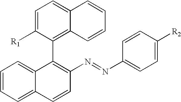


Priority Applications (2)
| Application Number | Priority Date | Filing Date | Title |
|---|---|---|---|
| US11/762,174 US8329058B2 (en) | 2004-01-28 | 2007-06-13 | Chiral nematic photo displays |
| US12/217,158 US8199086B2 (en) | 2004-01-28 | 2008-07-01 | Stacked color photodisplay |
Applications Claiming Priority (5)
| Application Number | Priority Date | Filing Date | Title |
|---|---|---|---|
| US53987304P | 2004-01-28 | 2004-01-28 | |
| US56558604P | 2004-04-27 | 2004-04-27 | |
| US11/006,100 US7236151B2 (en) | 2004-01-28 | 2004-12-07 | Liquid crystal display |
| US11/697,514 US20100157180A1 (en) | 2004-01-28 | 2007-04-06 | Liquid crystal display |
| US11/762,174 US8329058B2 (en) | 2004-01-28 | 2007-06-13 | Chiral nematic photo displays |
Related Parent Applications (1)
| Application Number | Title | Priority Date | Filing Date |
|---|---|---|---|
| US11/697,514 Continuation-In-Part US20100157180A1 (en) | 2004-01-28 | 2007-04-06 | Liquid crystal display |
Related Child Applications (1)
| Application Number | Title | Priority Date | Filing Date |
|---|---|---|---|
| US12/217,158 Continuation-In-Part US8199086B2 (en) | 2004-01-28 | 2008-07-01 | Stacked color photodisplay |
Publications (2)
| Publication Number | Publication Date |
|---|---|
| US20070237906A1 true US20070237906A1 (en) | 2007-10-11 |
| US8329058B2 US8329058B2 (en) | 2012-12-11 |
Family
ID=34799366
Family Applications (2)
| Application Number | Title | Priority Date | Filing Date |
|---|---|---|---|
| US11/006,100 Active US7236151B2 (en) | 2003-07-02 | 2004-12-07 | Liquid crystal display |
| US11/762,174 Active 2027-08-06 US8329058B2 (en) | 2004-01-28 | 2007-06-13 | Chiral nematic photo displays |
Family Applications Before (1)
| Application Number | Title | Priority Date | Filing Date |
|---|---|---|---|
| US11/006,100 Active US7236151B2 (en) | 2003-07-02 | 2004-12-07 | Liquid crystal display |
Country Status (4)
| Country | Link |
|---|---|
| US (2) | US7236151B2 (en) |
| CN (1) | CN1993725B (en) |
| GB (2) | GB2442651B (en) |
| WO (1) | WO2005072304A2 (en) |
Cited By (22)
| Publication number | Priority date | Publication date | Assignee | Title |
|---|---|---|---|---|
| US20080309598A1 (en) * | 2004-01-28 | 2008-12-18 | Doane J William | Stacked color photodisplay |
| US20090033811A1 (en) * | 2007-07-31 | 2009-02-05 | Kent Displays Incorporated | Multiple color writing tablet |
| US20090096942A1 (en) * | 2007-07-31 | 2009-04-16 | Kent Displays Incorporated | Selectively erasable electronic writing tablet |
| US20100157180A1 (en) * | 2004-01-28 | 2010-06-24 | Kent Displays Incorporated | Liquid crystal display |
| US20100265214A1 (en) * | 2007-07-31 | 2010-10-21 | Kent Displays Incorporated | Writing tablet information recording device |
| US20100263244A1 (en) * | 2009-04-16 | 2010-10-21 | Nelson Tabirian | Labels and taggants with programmable multi color coded timing |
| US20100317951A1 (en) * | 2009-06-11 | 2010-12-16 | Roche Diagnostics Operations, Inc. | Portable handheld medical diagnostic devices with color-changing indicator |
| WO2012051127A2 (en) * | 2010-10-12 | 2012-04-19 | Kent State University | A liquid crystal composition containing chiral dopant, device thereof, and methods thereof |
| US20130093969A1 (en) * | 2010-05-03 | 2013-04-18 | Kent State University | Smart photochromic chiral nematic liquid crystal window |
| US9116379B2 (en) | 2012-05-22 | 2015-08-25 | Kent Displays Incorporated | Electronic display with semitransparent back layer |
| US9134561B2 (en) | 2011-11-01 | 2015-09-15 | Kent Displays Incorporated | Writing tablet information recording device |
| US9235075B2 (en) | 2012-05-22 | 2016-01-12 | Kent Displays Incorporated | Electronic display with patterned layer |
| CN106833680A (en) * | 2017-01-03 | 2017-06-13 | 复旦大学 | A kind of photoresponse three-stable state chiral molecules material and its preparation method and application |
| WO2017214469A1 (en) * | 2016-06-10 | 2017-12-14 | University Of Pittsburgh-Of The Commonwealth System Of Higher Education | Optically transparent polymeric actuator and display apparatus employing same |
| US9851612B2 (en) | 2014-04-02 | 2017-12-26 | Kent Displays Inc. | Liquid crystal display with identifiers |
| CN107903916A (en) * | 2017-11-29 | 2018-04-13 | 北京化工大学 | Application and UV detector of the cholesteric liquid-crystal composition in ultraviolet light detection |
| US10088701B2 (en) | 2013-11-01 | 2018-10-02 | Kent Displays Inc. | Electronic writing device with dot pattern recognition system |
| CN109161385A (en) * | 2018-07-24 | 2019-01-08 | 华中科技大学 | A kind of liquid crystal material of cholesteric phase of visible light regulation color |
| US10473972B2 (en) * | 2016-08-12 | 2019-11-12 | Boe Technology Group Co., Ltd. | Polarization switching device and its driving method, and corresponding display apparatus |
| KR20200009803A (en) * | 2018-07-20 | 2020-01-30 | 한국화학연구원 | Surface energy controlled photoresponsive chiral dopants for cholesteric liquid crystal composition |
| US11439433B2 (en) | 2016-06-10 | 2022-09-13 | University of Pittsburgh—of the Commonwealth System of Higher Education | Optically transparent polymeric actuator and display apparatus employing same |
| US11809935B2 (en) * | 2019-10-03 | 2023-11-07 | United States Postal Service | Dynamically modifying the presentation of an e-label |
Families Citing this family (62)
| Publication number | Priority date | Publication date | Assignee | Title |
|---|---|---|---|---|
| US8052061B2 (en) * | 2002-08-07 | 2011-11-08 | Vanguard Identification Systems, Inc. | Permanent RFID luggage tag with security features |
| US7845569B1 (en) | 1999-06-16 | 2010-12-07 | Vanguard Identification Systems, Inc. | Permanent RFID luggage tag with security features |
| WO2005081779A2 (en) * | 2004-02-19 | 2005-09-09 | Kent Displays Incorporated | Staked display with shared electrode addressing |
| US7236151B2 (en) * | 2004-01-28 | 2007-06-26 | Kent Displays Incorporated | Liquid crystal display |
| US7190337B2 (en) * | 2003-07-02 | 2007-03-13 | Kent Displays Incorporated | Multi-configuration display driver |
| CN100513158C (en) * | 2004-01-28 | 2009-07-15 | 肯特显示器公司 | Liquid crystal display film |
| CN1975521A (en) * | 2004-01-28 | 2007-06-06 | 肯特显示器公司 | Liquid crystal display |
| JP2008501133A (en) * | 2004-05-28 | 2008-01-17 | コーニンクレッカ フィリップス エレクトロニクス エヌ ヴィ | Flexible flat panel display |
| WO2006053319A2 (en) * | 2004-11-12 | 2006-05-18 | Kent Displays Incorporated | Display device with electrical zipper interconnect |
| US20060202925A1 (en) * | 2004-12-07 | 2006-09-14 | William Manning | Remote cholesteric display |
| JP2006215477A (en) * | 2005-02-07 | 2006-08-17 | Nhk Spring Co Ltd | Discrimination medium and article provided with discrimination medium |
| US20060204675A1 (en) * | 2005-03-08 | 2006-09-14 | Eastman Kodak Company | Display device with improved flexibility |
| JP2007076156A (en) * | 2005-09-14 | 2007-03-29 | Brother Ind Ltd | Printer |
| US7791700B2 (en) * | 2005-09-16 | 2010-09-07 | Kent Displays Incorporated | Liquid crystal display on a printed circuit board |
| US7843411B2 (en) * | 2006-01-18 | 2010-11-30 | Manning Ventures, Inc. | Remote cholesteric display |
| US20070195399A1 (en) * | 2006-02-23 | 2007-08-23 | Eastman Kodak Company | Stacked-cell display with field isolation layer |
| US8022292B2 (en) * | 2006-10-02 | 2011-09-20 | SolASE Corporation | Photovoltaic device employing a resonator cavity |
| EP1939794A3 (en) | 2006-12-29 | 2009-04-01 | Vanguard Identification Systems, Inc. | Printed planar RFID element wristbands and like personal identification devices |
| KR101408510B1 (en) * | 2007-05-18 | 2014-06-17 | 삼성전자주식회사 | Flexible Substrate for Display and Device Using The Same |
| DE102007032169A1 (en) | 2007-07-10 | 2009-01-15 | Fraunhofer-Gesellschaft zur Förderung der angewandten Forschung e.V. | Display cell with kompartimentierter liquid crystal layer, process for their preparation and suitable for this, containing a liquid crystal material mixture |
| US8138939B2 (en) * | 2007-07-24 | 2012-03-20 | Manning Ventures, Inc. | Drug dispenser/container display |
| US9333728B2 (en) | 2007-11-06 | 2016-05-10 | Guardian Industries Corp. | Ruggedized switchable glazing, and/or method of making the same |
| US8199264B2 (en) | 2007-11-26 | 2012-06-12 | Guardian Industries Corp. | Ruggedized switchable glazing comprising a liquid crystal inclusive layer and a multi-layer low-E ultraviolet blocking coating |
| US8054391B2 (en) * | 2008-03-28 | 2011-11-08 | Motorola Mobility, Inc. | Semi-transparent display apparatus |
| US8310630B2 (en) | 2008-05-16 | 2012-11-13 | Manning Ventures, Inc. | Electronic skin having uniform gray scale reflectivity |
| US8334961B2 (en) * | 2008-09-10 | 2012-12-18 | Kent Displays Incorporated | Electrooptical display with electrical crossover |
| US8637331B2 (en) | 2008-10-17 | 2014-01-28 | Bloominescence, Llc | Transparent polarized light-emitting device |
| US20100141689A1 (en) * | 2008-12-04 | 2010-06-10 | Kent Displays, Inc. | Electronic skin reader |
| US8213309B2 (en) * | 2008-12-22 | 2012-07-03 | Broadcom Corporation | Systems and methods for reducing latency and reservation request overhead in a communications network |
| US8427615B2 (en) * | 2009-03-05 | 2013-04-23 | Kent State University | Transparent conducting electrodes and method for producing |
| US8176924B2 (en) * | 2009-03-11 | 2012-05-15 | Kent Displays Incorporated | Color changing artificial fingernails |
| US8760415B2 (en) * | 2009-03-30 | 2014-06-24 | Kent Displays Incorporated | Display with overlayed electronic skin |
| US9224084B2 (en) | 2009-04-01 | 2015-12-29 | Vanguard Identification Systems, Inc. | Smart device programmable electronic luggage tag |
| US9918537B2 (en) | 2009-04-01 | 2018-03-20 | Vanguard Identification Systems | Smart device programmable electronic luggage tag and bag mountings therefore |
| US7837897B2 (en) * | 2009-04-27 | 2010-11-23 | Polytronix, Inc. | Polymeric dispersed liquid crystal light shutter device |
| US8576209B2 (en) | 2009-07-07 | 2013-11-05 | Semiconductor Energy Laboratory Co., Ltd. | Display device |
| KR101587124B1 (en) * | 2009-09-23 | 2016-01-21 | 삼성디스플레이 주식회사 | Liquid crystal display including the same |
| US20110140844A1 (en) | 2009-12-15 | 2011-06-16 | Mcguire Kenneth Stephen | Packaged product having a reactive label and a method of its use |
| WO2011082086A1 (en) * | 2009-12-29 | 2011-07-07 | Qualcomm Mems Technologies, Inc. | Illumination device with metalized light-turning features |
| US20110199328A1 (en) * | 2010-02-18 | 2011-08-18 | Flextronics Ap, Llc | Touch screen system with acoustic and capacitive sensing |
| KR20120066354A (en) * | 2010-12-14 | 2012-06-22 | 삼성모바일디스플레이주식회사 | Substrate and display device including the same |
| TWI407191B (en) | 2010-12-24 | 2013-09-01 | Ind Tech Res Inst | Cholesteric liquid crystal display and displaying method of cholesteric liquid crystal display |
| US9117952B2 (en) | 2011-02-10 | 2015-08-25 | Lg Chem, Ltd. | Front sheet of solar cell, method of manufacturing the same and photovoltaic module comprising the same |
| US9651813B2 (en) | 2011-09-16 | 2017-05-16 | Kent Displays Inc. | Liquid crystal paper |
| US9245492B2 (en) | 2012-06-28 | 2016-01-26 | Intermec Ip Corp. | Dual screen display for mobile computing device |
| CN103033969B (en) * | 2013-01-05 | 2015-06-24 | 北京三五九投资有限公司 | Method for preparing printed flexible display module based on double-layer PDLC (Polymer Dispersed Liquid Crystal) |
| WO2014210165A2 (en) * | 2013-06-25 | 2014-12-31 | Kent State University | Polymer-dispersed blue-phase liquid crystal films |
| US10031364B2 (en) | 2013-06-25 | 2018-07-24 | Kent State University | Polymer-dispersed blue-phase liquid crystal films |
| JP2015215420A (en) * | 2014-05-08 | 2015-12-03 | 大日本印刷株式会社 | Light control film and light control device |
| JP2015215418A (en) * | 2014-05-08 | 2015-12-03 | 大日本印刷株式会社 | Light control film and light control device |
| US9517721B2 (en) | 2014-08-22 | 2016-12-13 | Guardian Industries Corp. | Vehicle sunroof with switchable glazing and side-firing light emitting diodes |
| WO2017006994A1 (en) * | 2015-07-09 | 2017-01-12 | シャープ株式会社 | Active matrix substrate, display device and production method |
| CN106588866B (en) * | 2016-11-21 | 2018-12-04 | 北京化工大学 | Chiral fluorescent molecule photoswitch and preparation method thereof, cholesteric liquid-crystal composition and preparation method thereof and liquid crystal display |
| KR20180070262A (en) * | 2016-12-16 | 2018-06-26 | 엘지디스플레이 주식회사 | Substrate, Liquid Crystal Display Device Including The Same And Method Of Fabricating The Same |
| CN106782094A (en) * | 2017-01-12 | 2017-05-31 | 京东方科技集团股份有限公司 | A kind of motherboard and preparation method thereof, cover plate and preparation method thereof, display device |
| CN108878665B (en) * | 2017-05-12 | 2021-01-26 | 京东方科技集团股份有限公司 | Organic electroluminescent device, preparation method thereof and display device |
| CN109031738A (en) | 2017-06-12 | 2018-12-18 | 江苏和成显示科技有限公司 | A kind of liquid crystal display device and its application |
| US10849557B2 (en) * | 2018-03-28 | 2020-12-01 | Apple Inc. | Fabric-based items with stretchable bands |
| DE102019119138B4 (en) * | 2019-07-15 | 2022-01-20 | Deutsche Post Ag | Determination of distribution and/or sorting information for the automated distribution and/or sorting of a shipment |
| CN112635103B (en) * | 2020-12-18 | 2022-07-29 | 深圳先进技术研究院 | Conductive pattern, preparation method thereof and flexible electronic device |
| JP2022112403A (en) * | 2021-01-21 | 2022-08-02 | 株式会社Joled | Display device |
| US11567375B2 (en) * | 2021-01-29 | 2023-01-31 | Meta Platforms, Inc. | Techniques for complex wavefront modulation |
Citations (91)
| Publication number | Priority date | Publication date | Assignee | Title |
|---|---|---|---|---|
| US3600060A (en) * | 1968-02-23 | 1971-08-17 | Ncr Co | Display device containing minute droplets of cholesteric liquid crystals in a substantially continuous polymeric matrix |
| US3680950A (en) * | 1971-03-15 | 1972-08-01 | Xerox Corp | Grandjean state liquid crystalline imaging system |
| US4362903A (en) * | 1980-12-29 | 1982-12-07 | General Electric Company | Electrical conductor interconnect providing solderable connections to hard-to-contact substrates, such as liquid crystal cells |
| US4510188A (en) * | 1982-03-11 | 1985-04-09 | Cinzia Ruggeri | Textile material of a dark fabric, leather or hide with layer of microencapsulated liquid crystals |
| US4566935A (en) * | 1984-07-31 | 1986-01-28 | Texas Instruments Incorporated | Spatial light modulator and method |
| US4642250A (en) * | 1986-01-13 | 1987-02-10 | Donald Spector | Fabrics and garments formed thereby having thermally-sensitive chromatic properties |
| US4680579A (en) * | 1983-09-08 | 1987-07-14 | Texas Instruments Incorporated | Optical system for projection display using spatial light modulator device |
| US4684771A (en) * | 1984-05-18 | 1987-08-04 | Sprecher & Schuh Ag | Vacuum switch |
| US4688900A (en) * | 1984-03-19 | 1987-08-25 | Kent State University | Light modulating material comprising a liquid crystal dispersion in a plastic matrix |
| US4747413A (en) * | 1986-11-07 | 1988-05-31 | Bloch Harry S | Infant temperature measuring apparatus and methods |
| US4890902A (en) * | 1985-09-17 | 1990-01-02 | Kent State University | Liquid crystal light modulating materials with selectable viewing angles |
| US4896946A (en) * | 1985-05-13 | 1990-01-30 | Ricoh Company, Ltd. | Liquid crystal display device |
| US4948232A (en) * | 1983-12-16 | 1990-08-14 | Alf Lange | Device for the presentation of information with rollable plastic substrate |
| US5007872A (en) * | 1989-06-12 | 1991-04-16 | Babcock Display Products, Inc. | Screened interconnect system |
| US5061553A (en) * | 1987-02-25 | 1991-10-29 | Olsen Jr Kenneth F | Coextruded sail |
| US5155607A (en) * | 1990-03-16 | 1992-10-13 | Fuji Xerox Co., Ltd. | Optical modulation display device and display method using the same |
| US5161479A (en) * | 1992-04-07 | 1992-11-10 | North Sails Group, Inc. | Laminated sail fabric |
| US5172108A (en) * | 1988-02-15 | 1992-12-15 | Nec Corporation | Multilevel image display method and system |
| US5200845A (en) * | 1989-10-31 | 1993-04-06 | University Of Hawaii At Manoa | Color liquid crystal display consisting of polymer-dispersed chiral liquid crystal having negative dielectric anisotropy |
| US5360503A (en) * | 1990-12-19 | 1994-11-01 | Aerospatiale | Semi-finished product and thermoplastic composite material having liquid crystal polymers and process for the production of the material |
| US5376699A (en) * | 1992-04-08 | 1994-12-27 | Merck Patent Gesellschaft Mit Beschrankter Haftung | Surface coating medium |
| US5437811A (en) * | 1991-05-02 | 1995-08-01 | Kent State University | Liquid crystalline light modulating device and material |
| US5453863A (en) * | 1991-05-02 | 1995-09-26 | Kent State University | Multistable chiral nematic displays |
| US5493430A (en) * | 1994-08-03 | 1996-02-20 | Kent Display Systems, L.P. | Color, reflective liquid crystal displays |
| US5530457A (en) * | 1993-11-09 | 1996-06-25 | Honeywell Inc. | Partitioned display apparatus |
| US5625477A (en) * | 1994-04-11 | 1997-04-29 | Advanced Display Systems, Inc. | Zero field multistable cholesteric liquid crystal displays |
| US5636044A (en) * | 1994-10-14 | 1997-06-03 | Kent Displays, Inc. | Segmented polymer stabilized and polymer free cholesteric texture liquid crystal displays and driving method for same |
| US5644330A (en) * | 1994-08-11 | 1997-07-01 | Kent Displays, Inc. | Driving method for polymer stabilized and polymer free liquid crystal displays |
| US5668614A (en) * | 1995-05-01 | 1997-09-16 | Kent State University | Pixelized liquid crystal display materials including chiral material adopted to change its chirality upon photo-irradiation |
| US20010015712A1 (en) * | 2000-02-14 | 2001-08-23 | Nec Corporation | Device circuit of display unit |
| US6307605B1 (en) * | 1997-07-25 | 2001-10-23 | Eveready Battery Company, Inc. | Liquid crystal display and battery label including a liquid crystal display |
| US6316278B1 (en) * | 1999-03-16 | 2001-11-13 | Alien Technology Corporation | Methods for fabricating a multiple modular assembly |
| US6320563B1 (en) * | 1999-01-21 | 2001-11-20 | Kent State University | Dual frequency cholesteric display and drive scheme |
| US20020030776A1 (en) * | 1999-08-23 | 2002-03-14 | Kent Displays Incorporated | Back lit cholesteric liquid crystal display |
| US20020030786A1 (en) * | 1999-06-21 | 2002-03-14 | Stanley W. Stephenson | Sheet having a layer with different light modulating materials |
| US6377321B1 (en) * | 1997-03-22 | 2002-04-23 | Kent Displays, Inc. | Stacked color liquid crystal display device |
| US6423368B1 (en) * | 2000-01-06 | 2002-07-23 | Eastman Kodak Company | Method for making materials having uniform limited coalescence domains |
| US6433849B1 (en) * | 1999-01-23 | 2002-08-13 | International Business Machines Corporation | High reflectivity bistable liquid crystal display |
| US6452590B1 (en) * | 1999-01-14 | 2002-09-17 | Fujitsu Limited | Method and device for driving a display panel |
| US6459467B1 (en) * | 1998-05-15 | 2002-10-01 | Minolta Co., Ltd. | Liquid crystal light modulating device, and a manufacturing method and a manufacturing apparatus thereof |
| US6468638B2 (en) * | 1999-03-16 | 2002-10-22 | Alien Technology Corporation | Web process interconnect in electronic assemblies |
| US6483563B2 (en) * | 1999-08-23 | 2002-11-19 | Kent Displays, Inc. | Brightness enhancement for bistable cholesteric displays |
| US20020186182A1 (en) * | 2001-05-09 | 2002-12-12 | Eastman Kodak Company | Drive for cholesteric liquid crystal displays |
| US20030011549A1 (en) * | 2001-06-29 | 2003-01-16 | Shunichi Murahashi | Liquid crystal driving devices |
| US20030016329A1 (en) * | 2001-07-21 | 2003-01-23 | Eastman Kodak Company | Making a liquid crystal display using heat and pressure lamination of liquid crystal coating |
| US20030019575A1 (en) * | 2001-07-26 | 2003-01-30 | Eastman Kodak Company | Method of making liquid crystal display having a dielectric adhesive layer for laminating a liquid cryatal layer |
| US20030031845A1 (en) * | 2000-12-27 | 2003-02-13 | Masanori Umeya | Liquid crystal transfer body and method of transferring the liquid crystal transfer body |
| US20030034945A1 (en) * | 2001-08-07 | 2003-02-20 | Eastman Kodak Company | Gray scale and color cholesteric liquid crystal displays |
| US20030063245A1 (en) * | 2001-09-21 | 2003-04-03 | Bowley Christopher C. | Cholesteric liquid crystal optical bodies and methods of manufacture and use |
| US20030071791A1 (en) * | 2001-10-11 | 2003-04-17 | Palm, Inc. | Accessory module for handheld devices |
| US6556262B1 (en) * | 2000-01-06 | 2003-04-29 | Eastman Kodak Company | Display sheet having memory using limited coalescence domains |
| US20030085380A1 (en) * | 1999-02-17 | 2003-05-08 | Basf Aktiengesellschaft | Cholesteric layered material, and the production thereof |
| US20030117548A1 (en) * | 2001-12-26 | 2003-06-26 | Eastman Kodak Company | Field spreading layer for dispersed liquid crystal coatings |
| US6603259B1 (en) * | 1999-03-12 | 2003-08-05 | Visson Ip, Llc | Electroluminescent device and method of manufacturing same |
| US6608438B2 (en) * | 2001-11-09 | 2003-08-19 | Visson Ip Llc | 3-D flexible display structure |
| US20030155151A1 (en) * | 2001-04-25 | 2003-08-21 | Anno Hermanns | Electrical contacts for flexible displays |
| US20030160912A1 (en) * | 2002-02-28 | 2003-08-28 | Eastman Kodak Company | Transaction card with memory and polymer dispersed cholesteric liquid crystal display |
| US6618114B2 (en) * | 2001-02-12 | 2003-09-09 | Viztec, Inc. | Electrooptical displays with multilayer structure achieved by varying rates of polymerization and/or phase separation during the course of polymerization |
| US20030169221A1 (en) * | 2002-03-08 | 2003-09-11 | Eastman Kodak Company | Unipolar drive chip for cholesteric liquid crystal displays |
| US6624565B2 (en) * | 2001-07-05 | 2003-09-23 | Visson Ip, Llc | Cellular flexible display structure |
| US6628256B2 (en) * | 1999-12-03 | 2003-09-30 | Nec Lcd Technologies, Ltd. | Drive circuit of a liquid crystal display device |
| US20030184569A1 (en) * | 2002-03-28 | 2003-10-02 | Nec Corporation | Image display method and image display device |
| US6639578B1 (en) * | 1995-07-20 | 2003-10-28 | E Ink Corporation | Flexible displays |
| US20030202136A1 (en) * | 2002-04-29 | 2003-10-30 | Eastman Kodak Company | Display having front contacts and printable area |
| US20030206147A1 (en) * | 2002-05-03 | 2003-11-06 | Eastman Kodak Company | General 2 voltage levels driving scheme for cholesterical liquid crystal displays |
| US6657620B2 (en) * | 2000-03-21 | 2003-12-02 | Pioneer Corporation | Flat panel type display apparatus |
| US6655788B1 (en) * | 2002-05-17 | 2003-12-02 | Viztec Inc. | Composite structure for enhanced flexibility of electro-optic displays with sliding layers |
| US20030222139A1 (en) * | 2002-06-04 | 2003-12-04 | Eastman Kodak Company | Item tag with liquid crystal display and image |
| US20040032545A1 (en) * | 2002-08-16 | 2004-02-19 | Eastman Kodak Company | Pigment layer for polymer-dispersed liquid crystal displays |
| US6697191B2 (en) * | 2001-06-11 | 2004-02-24 | Visson Ip, Llc | Electro-optical display |
| US6710760B1 (en) * | 2000-11-28 | 2004-03-23 | Eastman Kodak Company | Unipolar drive for cholesteric liquid crystal displays |
| US6723479B2 (en) * | 2000-04-25 | 2004-04-20 | Koninklijke Philips Electronics N.V. | Method for providing a surface of an article with a decoration or text |
| US6727197B1 (en) * | 1999-11-18 | 2004-04-27 | Foster-Miller, Inc. | Wearable transmission device |
| US20040080477A1 (en) * | 2002-10-29 | 2004-04-29 | Eastman Kodak Company | Docking station for writing to electronically writable display |
| US20040105614A1 (en) * | 2002-11-29 | 2004-06-03 | Fuji Xerox Co., Ltd. | Optical switching element and photoaddressable display medium using the same |
| US6811815B2 (en) * | 2002-06-14 | 2004-11-02 | Avery Dennison Corporation | Method for roll-to-roll deposition of optically transparent and high conductivity metallic thin films |
| US6819310B2 (en) * | 2000-04-27 | 2004-11-16 | Manning Ventures, Inc. | Active matrix addressed bistable reflective cholesteric displays |
| US20050001797A1 (en) * | 2003-07-02 | 2005-01-06 | Miller Nick M. | Multi-configuration display driver |
| US20050007336A1 (en) * | 1997-08-28 | 2005-01-13 | E Ink Corporation | Adhesive backed displays |
| US6850217B2 (en) * | 2000-04-27 | 2005-02-01 | Manning Ventures, Inc. | Operating method for active matrix addressed bistable reflective cholesteric displays |
| US20050079386A1 (en) * | 2003-10-01 | 2005-04-14 | Board Of Regents, The University Of Texas System | Compositions, methods and systems for making and using electronic paper |
| US20050083284A1 (en) * | 2000-04-27 | 2005-04-21 | Manning Ventures-Inc. | Graphic controller for active matrix addressed bistable reflective Cholesteric displays |
| US6893585B2 (en) * | 2001-09-17 | 2005-05-17 | Fuji Photo Film Co., Ltd. | Liquid crystal composition, selectively reflective film and method for producing the same |
| US6902454B1 (en) * | 2000-07-28 | 2005-06-07 | Eastman Kodak Company | Process for laminating electrically addressable display |
| US20050195354A1 (en) * | 2003-07-02 | 2005-09-08 | Doane Joseph W. | Single substrate liquid crystal display |
| US20060124899A1 (en) * | 2004-12-15 | 2006-06-15 | Eastman Kodak Company | Photochemically active chiral compounds and compositions containing the same |
| US20060204675A1 (en) * | 2005-03-08 | 2006-09-14 | Eastman Kodak Company | Display device with improved flexibility |
| US20070059901A1 (en) * | 2005-09-15 | 2007-03-15 | Eastman Kodak Company | Metal and electronically conductive polymer transfer |
| US7236151B2 (en) * | 2004-01-28 | 2007-06-26 | Kent Displays Incorporated | Liquid crystal display |
| US20070285385A1 (en) * | 1998-11-02 | 2007-12-13 | E Ink Corporation | Broadcast system for electronic ink signs |
| US20080309598A1 (en) * | 2004-01-28 | 2008-12-18 | Doane J William | Stacked color photodisplay |
Family Cites Families (30)
| Publication number | Priority date | Publication date | Assignee | Title |
|---|---|---|---|---|
| US5847798A (en) | 1991-05-02 | 1998-12-08 | Kent State University | Polymer stabilized black-white cholesteric reflective display |
| KR100320567B1 (en) | 1992-05-18 | 2002-06-20 | Liquid Crystal Light Modulators & Materials | |
| TW247359B (en) | 1993-08-30 | 1995-05-11 | Hitachi Seisakusyo Kk | Liquid crystal display and liquid crystal driver |
| US6154190A (en) | 1995-02-17 | 2000-11-28 | Kent State University | Dynamic drive methods and apparatus for a bistable liquid crystal display |
| US5748277A (en) | 1995-02-17 | 1998-05-05 | Kent State University | Dynamic drive method and apparatus for a bistable liquid crystal display |
| US5751257A (en) | 1995-04-28 | 1998-05-12 | Teletransactions, Inc. | Programmable shelf tag and method for changing and updating shelf tag information |
| US6269342B1 (en) | 1995-04-28 | 2001-07-31 | Telxon Corporation | Programmable shelf tag system |
| US5734155A (en) | 1995-06-07 | 1998-03-31 | Lsi Logic Corporation | Photo-sensitive semiconductor integrated circuit substrate and systems containing the same |
| JP3735374B2 (en) | 1995-08-01 | 2006-01-18 | オーストリア カード プラスティッカルテン ウント アウスヴァイスジステーム ゲゼルシャフト ミット ベシュレンクテル ハフツング | Data carrier having a module including a component and having a coil and method of manufacturing the same |
| US6271898B1 (en) | 1996-09-19 | 2001-08-07 | Rohm And Haas Company | Particles and droplets containing liquid domains and method for forming in an aqueous medium |
| JPH09120079A (en) | 1995-10-26 | 1997-05-06 | Hitachi Ltd | Liquid crystal display device |
| JP3656772B2 (en) * | 1995-12-26 | 2005-06-08 | 大日本印刷株式会社 | Thermal transfer sheet, printed matter and recording method |
| US6061107A (en) | 1996-05-10 | 2000-05-09 | Kent State University | Bistable polymer dispersed cholesteric liquid crystal displays |
| US6133895A (en) | 1997-06-04 | 2000-10-17 | Kent Displays Incorporated | Cumulative drive scheme and method for a liquid crystal display |
| CA2242217C (en) | 1997-07-10 | 2006-12-12 | Kuraray Co., Ltd. | Screen textile material |
| GB2333174A (en) | 1998-01-09 | 1999-07-14 | Sharp Kk | Data line driver for an active matrix display |
| US6096666A (en) | 1998-04-29 | 2000-08-01 | Motorola, Inc. | Holographic textile fiber |
| US6268839B1 (en) | 1998-05-12 | 2001-07-31 | Kent State University | Drive schemes for gray scale bistable cholesteric reflective displays |
| US6278429B1 (en) | 1998-09-11 | 2001-08-21 | Kent State University | Bistable reflective cholesteric liquid crystal displays utilizing super twisted nematic driver chips |
| US6072619A (en) | 1999-03-22 | 2000-06-06 | Visson Ip, Llc | Electro-optical light modulating device |
| US6277439B1 (en) | 1999-04-26 | 2001-08-21 | Pittards Public Limited Company | Impregnation of leather with micro-encapsulated material |
| US6781666B2 (en) | 1999-07-16 | 2004-08-24 | Minolta Co., Ltd. | Liquid crystal display and method to manufacture the same |
| US6270783B1 (en) | 1999-08-13 | 2001-08-07 | Unilever Home & Personal Care Usa, Division Of Conopco, Inc. | Cosmetic strips with liquid crystal temperature dependent color change |
| JP2001066573A (en) | 1999-08-31 | 2001-03-16 | Minolta Co Ltd | Information display device |
| US6518944B1 (en) | 1999-10-25 | 2003-02-11 | Kent Displays, Inc. | Combined cholesteric liquid crystal display and solar cell assembly device |
| JP2002341320A (en) * | 2001-05-15 | 2002-11-27 | Fuji Photo Film Co Ltd | Liquid crystal display device and optical laminate |
| WO2003015918A2 (en) | 2001-08-16 | 2003-02-27 | Weidmann Plastics Technology Ag | Method for the production of a sealing cover and sealing cover produced by said method |
| JP4004908B2 (en) | 2002-09-26 | 2007-11-07 | 富士通株式会社 | Display device driving method and apparatus |
| WO2005081779A2 (en) | 2004-02-19 | 2005-09-09 | Kent Displays Incorporated | Staked display with shared electrode addressing |
| CN1975521A (en) | 2004-01-28 | 2007-06-06 | 肯特显示器公司 | Liquid crystal display |
-
2004
- 2004-12-07 US US11/006,100 patent/US7236151B2/en active Active
-
2005
- 2005-01-24 WO PCT/US2005/002170 patent/WO2005072304A2/en active Application Filing
- 2005-01-24 CN CN2005800033964A patent/CN1993725B/en not_active Expired - Fee Related
- 2005-01-24 GB GB0800743A patent/GB2442651B/en not_active Expired - Fee Related
- 2005-01-24 GB GB0613888A patent/GB2426114B/en not_active Expired - Fee Related
-
2007
- 2007-06-13 US US11/762,174 patent/US8329058B2/en active Active
Patent Citations (99)
| Publication number | Priority date | Publication date | Assignee | Title |
|---|---|---|---|---|
| US3600060A (en) * | 1968-02-23 | 1971-08-17 | Ncr Co | Display device containing minute droplets of cholesteric liquid crystals in a substantially continuous polymeric matrix |
| US3680950A (en) * | 1971-03-15 | 1972-08-01 | Xerox Corp | Grandjean state liquid crystalline imaging system |
| US4362903A (en) * | 1980-12-29 | 1982-12-07 | General Electric Company | Electrical conductor interconnect providing solderable connections to hard-to-contact substrates, such as liquid crystal cells |
| US4510188A (en) * | 1982-03-11 | 1985-04-09 | Cinzia Ruggeri | Textile material of a dark fabric, leather or hide with layer of microencapsulated liquid crystals |
| US4680579A (en) * | 1983-09-08 | 1987-07-14 | Texas Instruments Incorporated | Optical system for projection display using spatial light modulator device |
| US4948232A (en) * | 1983-12-16 | 1990-08-14 | Alf Lange | Device for the presentation of information with rollable plastic substrate |
| US4688900A (en) * | 1984-03-19 | 1987-08-25 | Kent State University | Light modulating material comprising a liquid crystal dispersion in a plastic matrix |
| US4684771A (en) * | 1984-05-18 | 1987-08-04 | Sprecher & Schuh Ag | Vacuum switch |
| US4566935A (en) * | 1984-07-31 | 1986-01-28 | Texas Instruments Incorporated | Spatial light modulator and method |
| US4896946A (en) * | 1985-05-13 | 1990-01-30 | Ricoh Company, Ltd. | Liquid crystal display device |
| US4890902A (en) * | 1985-09-17 | 1990-01-02 | Kent State University | Liquid crystal light modulating materials with selectable viewing angles |
| US4642250A (en) * | 1986-01-13 | 1987-02-10 | Donald Spector | Fabrics and garments formed thereby having thermally-sensitive chromatic properties |
| US4747413A (en) * | 1986-11-07 | 1988-05-31 | Bloch Harry S | Infant temperature measuring apparatus and methods |
| US5061553A (en) * | 1987-02-25 | 1991-10-29 | Olsen Jr Kenneth F | Coextruded sail |
| US5172108A (en) * | 1988-02-15 | 1992-12-15 | Nec Corporation | Multilevel image display method and system |
| US5007872A (en) * | 1989-06-12 | 1991-04-16 | Babcock Display Products, Inc. | Screened interconnect system |
| US5200845A (en) * | 1989-10-31 | 1993-04-06 | University Of Hawaii At Manoa | Color liquid crystal display consisting of polymer-dispersed chiral liquid crystal having negative dielectric anisotropy |
| US5155607A (en) * | 1990-03-16 | 1992-10-13 | Fuji Xerox Co., Ltd. | Optical modulation display device and display method using the same |
| US5360503A (en) * | 1990-12-19 | 1994-11-01 | Aerospatiale | Semi-finished product and thermoplastic composite material having liquid crystal polymers and process for the production of the material |
| US5453863A (en) * | 1991-05-02 | 1995-09-26 | Kent State University | Multistable chiral nematic displays |
| US5437811A (en) * | 1991-05-02 | 1995-08-01 | Kent State University | Liquid crystalline light modulating device and material |
| US5161479A (en) * | 1992-04-07 | 1992-11-10 | North Sails Group, Inc. | Laminated sail fabric |
| US5376699A (en) * | 1992-04-08 | 1994-12-27 | Merck Patent Gesellschaft Mit Beschrankter Haftung | Surface coating medium |
| US5530457A (en) * | 1993-11-09 | 1996-06-25 | Honeywell Inc. | Partitioned display apparatus |
| US5625477A (en) * | 1994-04-11 | 1997-04-29 | Advanced Display Systems, Inc. | Zero field multistable cholesteric liquid crystal displays |
| US5493430A (en) * | 1994-08-03 | 1996-02-20 | Kent Display Systems, L.P. | Color, reflective liquid crystal displays |
| US5644330A (en) * | 1994-08-11 | 1997-07-01 | Kent Displays, Inc. | Driving method for polymer stabilized and polymer free liquid crystal displays |
| US5636044A (en) * | 1994-10-14 | 1997-06-03 | Kent Displays, Inc. | Segmented polymer stabilized and polymer free cholesteric texture liquid crystal displays and driving method for same |
| US5668614A (en) * | 1995-05-01 | 1997-09-16 | Kent State University | Pixelized liquid crystal display materials including chiral material adopted to change its chirality upon photo-irradiation |
| US6639578B1 (en) * | 1995-07-20 | 2003-10-28 | E Ink Corporation | Flexible displays |
| US6654080B1 (en) * | 1997-03-22 | 2003-11-25 | Kent Displays, Inc. | Stacked color liquid crystal display device |
| US6377321B1 (en) * | 1997-03-22 | 2002-04-23 | Kent Displays, Inc. | Stacked color liquid crystal display device |
| US6307605B1 (en) * | 1997-07-25 | 2001-10-23 | Eveready Battery Company, Inc. | Liquid crystal display and battery label including a liquid crystal display |
| US20050007336A1 (en) * | 1997-08-28 | 2005-01-13 | E Ink Corporation | Adhesive backed displays |
| US6459467B1 (en) * | 1998-05-15 | 2002-10-01 | Minolta Co., Ltd. | Liquid crystal light modulating device, and a manufacturing method and a manufacturing apparatus thereof |
| US20070285385A1 (en) * | 1998-11-02 | 2007-12-13 | E Ink Corporation | Broadcast system for electronic ink signs |
| US6452590B1 (en) * | 1999-01-14 | 2002-09-17 | Fujitsu Limited | Method and device for driving a display panel |
| US6320563B1 (en) * | 1999-01-21 | 2001-11-20 | Kent State University | Dual frequency cholesteric display and drive scheme |
| US6433849B1 (en) * | 1999-01-23 | 2002-08-13 | International Business Machines Corporation | High reflectivity bistable liquid crystal display |
| US20030085380A1 (en) * | 1999-02-17 | 2003-05-08 | Basf Aktiengesellschaft | Cholesteric layered material, and the production thereof |
| US6603259B1 (en) * | 1999-03-12 | 2003-08-05 | Visson Ip, Llc | Electroluminescent device and method of manufacturing same |
| US6316278B1 (en) * | 1999-03-16 | 2001-11-13 | Alien Technology Corporation | Methods for fabricating a multiple modular assembly |
| US6468638B2 (en) * | 1999-03-16 | 2002-10-22 | Alien Technology Corporation | Web process interconnect in electronic assemblies |
| US20020030786A1 (en) * | 1999-06-21 | 2002-03-14 | Stanley W. Stephenson | Sheet having a layer with different light modulating materials |
| US6359673B1 (en) * | 1999-06-21 | 2002-03-19 | Eastman Kodak Company | Sheet having a layer with different light modulating materials |
| US6532052B1 (en) * | 1999-08-23 | 2003-03-11 | Kent Displays, Inc. | Brightness enhancement for bistable cholesteric displays |
| US7009666B2 (en) * | 1999-08-23 | 2006-03-07 | Kent Displays Incorporated | Back lit cholesteric liquid crystal display |
| US20020030776A1 (en) * | 1999-08-23 | 2002-03-14 | Kent Displays Incorporated | Back lit cholesteric liquid crystal display |
| US6483563B2 (en) * | 1999-08-23 | 2002-11-19 | Kent Displays, Inc. | Brightness enhancement for bistable cholesteric displays |
| US6727197B1 (en) * | 1999-11-18 | 2004-04-27 | Foster-Miller, Inc. | Wearable transmission device |
| US6628256B2 (en) * | 1999-12-03 | 2003-09-30 | Nec Lcd Technologies, Ltd. | Drive circuit of a liquid crystal display device |
| US6556262B1 (en) * | 2000-01-06 | 2003-04-29 | Eastman Kodak Company | Display sheet having memory using limited coalescence domains |
| US6423368B1 (en) * | 2000-01-06 | 2002-07-23 | Eastman Kodak Company | Method for making materials having uniform limited coalescence domains |
| US20010015712A1 (en) * | 2000-02-14 | 2001-08-23 | Nec Corporation | Device circuit of display unit |
| US6657620B2 (en) * | 2000-03-21 | 2003-12-02 | Pioneer Corporation | Flat panel type display apparatus |
| US6723479B2 (en) * | 2000-04-25 | 2004-04-20 | Koninklijke Philips Electronics N.V. | Method for providing a surface of an article with a decoration or text |
| US6850217B2 (en) * | 2000-04-27 | 2005-02-01 | Manning Ventures, Inc. | Operating method for active matrix addressed bistable reflective cholesteric displays |
| US6819310B2 (en) * | 2000-04-27 | 2004-11-16 | Manning Ventures, Inc. | Active matrix addressed bistable reflective cholesteric displays |
| US20050083284A1 (en) * | 2000-04-27 | 2005-04-21 | Manning Ventures-Inc. | Graphic controller for active matrix addressed bistable reflective Cholesteric displays |
| US6902454B1 (en) * | 2000-07-28 | 2005-06-07 | Eastman Kodak Company | Process for laminating electrically addressable display |
| US6710760B1 (en) * | 2000-11-28 | 2004-03-23 | Eastman Kodak Company | Unipolar drive for cholesteric liquid crystal displays |
| US20030031845A1 (en) * | 2000-12-27 | 2003-02-13 | Masanori Umeya | Liquid crystal transfer body and method of transferring the liquid crystal transfer body |
| US6618114B2 (en) * | 2001-02-12 | 2003-09-09 | Viztec, Inc. | Electrooptical displays with multilayer structure achieved by varying rates of polymerization and/or phase separation during the course of polymerization |
| US20030155151A1 (en) * | 2001-04-25 | 2003-08-21 | Anno Hermanns | Electrical contacts for flexible displays |
| US6864435B2 (en) * | 2001-04-25 | 2005-03-08 | Alien Technology Corporation | Electrical contacts for flexible displays |
| US20020186182A1 (en) * | 2001-05-09 | 2002-12-12 | Eastman Kodak Company | Drive for cholesteric liquid crystal displays |
| US6697191B2 (en) * | 2001-06-11 | 2004-02-24 | Visson Ip, Llc | Electro-optical display |
| US20030011549A1 (en) * | 2001-06-29 | 2003-01-16 | Shunichi Murahashi | Liquid crystal driving devices |
| US6624565B2 (en) * | 2001-07-05 | 2003-09-23 | Visson Ip, Llc | Cellular flexible display structure |
| US20030016329A1 (en) * | 2001-07-21 | 2003-01-23 | Eastman Kodak Company | Making a liquid crystal display using heat and pressure lamination of liquid crystal coating |
| US20030019575A1 (en) * | 2001-07-26 | 2003-01-30 | Eastman Kodak Company | Method of making liquid crystal display having a dielectric adhesive layer for laminating a liquid cryatal layer |
| US6585849B2 (en) * | 2001-07-26 | 2003-07-01 | Eastman Kodak Company | Method of making liquid crystal display having a dielectric adhesive layer for laminating a liquid crystal layer |
| US20030034945A1 (en) * | 2001-08-07 | 2003-02-20 | Eastman Kodak Company | Gray scale and color cholesteric liquid crystal displays |
| US6893585B2 (en) * | 2001-09-17 | 2005-05-17 | Fuji Photo Film Co., Ltd. | Liquid crystal composition, selectively reflective film and method for producing the same |
| US20030063245A1 (en) * | 2001-09-21 | 2003-04-03 | Bowley Christopher C. | Cholesteric liquid crystal optical bodies and methods of manufacture and use |
| US20030071791A1 (en) * | 2001-10-11 | 2003-04-17 | Palm, Inc. | Accessory module for handheld devices |
| US6608438B2 (en) * | 2001-11-09 | 2003-08-19 | Visson Ip Llc | 3-D flexible display structure |
| US20030117548A1 (en) * | 2001-12-26 | 2003-06-26 | Eastman Kodak Company | Field spreading layer for dispersed liquid crystal coatings |
| US20030160912A1 (en) * | 2002-02-28 | 2003-08-28 | Eastman Kodak Company | Transaction card with memory and polymer dispersed cholesteric liquid crystal display |
| US20030169221A1 (en) * | 2002-03-08 | 2003-09-11 | Eastman Kodak Company | Unipolar drive chip for cholesteric liquid crystal displays |
| US20030184569A1 (en) * | 2002-03-28 | 2003-10-02 | Nec Corporation | Image display method and image display device |
| US20030202136A1 (en) * | 2002-04-29 | 2003-10-30 | Eastman Kodak Company | Display having front contacts and printable area |
| US20030206147A1 (en) * | 2002-05-03 | 2003-11-06 | Eastman Kodak Company | General 2 voltage levels driving scheme for cholesterical liquid crystal displays |
| US6655788B1 (en) * | 2002-05-17 | 2003-12-02 | Viztec Inc. | Composite structure for enhanced flexibility of electro-optic displays with sliding layers |
| US20030222139A1 (en) * | 2002-06-04 | 2003-12-04 | Eastman Kodak Company | Item tag with liquid crystal display and image |
| US6811815B2 (en) * | 2002-06-14 | 2004-11-02 | Avery Dennison Corporation | Method for roll-to-roll deposition of optically transparent and high conductivity metallic thin films |
| US6788362B2 (en) * | 2002-08-16 | 2004-09-07 | Eastman Kodak Company | Pigment layer for polymer-dispersed liquid crystal displays |
| US20040032545A1 (en) * | 2002-08-16 | 2004-02-19 | Eastman Kodak Company | Pigment layer for polymer-dispersed liquid crystal displays |
| US20040080477A1 (en) * | 2002-10-29 | 2004-04-29 | Eastman Kodak Company | Docking station for writing to electronically writable display |
| US20040105614A1 (en) * | 2002-11-29 | 2004-06-03 | Fuji Xerox Co., Ltd. | Optical switching element and photoaddressable display medium using the same |
| US20050195354A1 (en) * | 2003-07-02 | 2005-09-08 | Doane Joseph W. | Single substrate liquid crystal display |
| US20050001797A1 (en) * | 2003-07-02 | 2005-01-06 | Miller Nick M. | Multi-configuration display driver |
| US7170481B2 (en) * | 2003-07-02 | 2007-01-30 | Kent Displays Incorporated | Single substrate liquid crystal display |
| US20050079386A1 (en) * | 2003-10-01 | 2005-04-14 | Board Of Regents, The University Of Texas System | Compositions, methods and systems for making and using electronic paper |
| US7236151B2 (en) * | 2004-01-28 | 2007-06-26 | Kent Displays Incorporated | Liquid crystal display |
| US20080309598A1 (en) * | 2004-01-28 | 2008-12-18 | Doane J William | Stacked color photodisplay |
| US20060124899A1 (en) * | 2004-12-15 | 2006-06-15 | Eastman Kodak Company | Photochemically active chiral compounds and compositions containing the same |
| US20060204675A1 (en) * | 2005-03-08 | 2006-09-14 | Eastman Kodak Company | Display device with improved flexibility |
| US20070059901A1 (en) * | 2005-09-15 | 2007-03-15 | Eastman Kodak Company | Metal and electronically conductive polymer transfer |
Cited By (33)
| Publication number | Priority date | Publication date | Assignee | Title |
|---|---|---|---|---|
| US8199086B2 (en) * | 2004-01-28 | 2012-06-12 | Kent Displays Incorporated | Stacked color photodisplay |
| US20100157180A1 (en) * | 2004-01-28 | 2010-06-24 | Kent Displays Incorporated | Liquid crystal display |
| US20080309598A1 (en) * | 2004-01-28 | 2008-12-18 | Doane J William | Stacked color photodisplay |
| US8228301B2 (en) | 2007-07-31 | 2012-07-24 | Kent Displays Incorporated | Multiple color writing tablet |
| US20100265214A1 (en) * | 2007-07-31 | 2010-10-21 | Kent Displays Incorporated | Writing tablet information recording device |
| US20090033811A1 (en) * | 2007-07-31 | 2009-02-05 | Kent Displays Incorporated | Multiple color writing tablet |
| US20090096942A1 (en) * | 2007-07-31 | 2009-04-16 | Kent Displays Incorporated | Selectively erasable electronic writing tablet |
| US8139039B2 (en) | 2007-07-31 | 2012-03-20 | Kent Displays, Incorporated | Selectively erasable electronic writing tablet |
| US20100263244A1 (en) * | 2009-04-16 | 2010-10-21 | Nelson Tabirian | Labels and taggants with programmable multi color coded timing |
| US20100317951A1 (en) * | 2009-06-11 | 2010-12-16 | Roche Diagnostics Operations, Inc. | Portable handheld medical diagnostic devices with color-changing indicator |
| US8501093B2 (en) | 2009-06-11 | 2013-08-06 | Roche Diagnostics Operations, Inc. | Portable handheld medical diagnostic devices with color-changing indicatior |
| US20130093969A1 (en) * | 2010-05-03 | 2013-04-18 | Kent State University | Smart photochromic chiral nematic liquid crystal window |
| US9063358B2 (en) * | 2010-05-03 | 2015-06-23 | Kent State University | Smart photochromic chiral nematic liquid crystal window |
| WO2012051127A2 (en) * | 2010-10-12 | 2012-04-19 | Kent State University | A liquid crystal composition containing chiral dopant, device thereof, and methods thereof |
| WO2012051127A3 (en) * | 2010-10-12 | 2012-08-02 | Kent State University | A liquid crystal composition containing chiral dopant, device thereof, and methods thereof |
| US9134561B2 (en) | 2011-11-01 | 2015-09-15 | Kent Displays Incorporated | Writing tablet information recording device |
| US9946106B2 (en) | 2012-05-22 | 2018-04-17 | Kent Displays Inc. | Electronic display with semitransparent back layer |
| US9235075B2 (en) | 2012-05-22 | 2016-01-12 | Kent Displays Incorporated | Electronic display with patterned layer |
| US9116379B2 (en) | 2012-05-22 | 2015-08-25 | Kent Displays Incorporated | Electronic display with semitransparent back layer |
| US10088701B2 (en) | 2013-11-01 | 2018-10-02 | Kent Displays Inc. | Electronic writing device with dot pattern recognition system |
| US9851612B2 (en) | 2014-04-02 | 2017-12-26 | Kent Displays Inc. | Liquid crystal display with identifiers |
| WO2017214469A1 (en) * | 2016-06-10 | 2017-12-14 | University Of Pittsburgh-Of The Commonwealth System Of Higher Education | Optically transparent polymeric actuator and display apparatus employing same |
| US11084982B2 (en) * | 2016-06-10 | 2021-08-10 | University Of Pittsburgh-Of The Commonwealth System Of Higher Education | Optically transparent polymeric actuator and display apparatus employing same |
| US11739268B2 (en) | 2016-06-10 | 2023-08-29 | University Of Pittsburgh-Of The Commonwealth System Of Higher Education | Optically transparent polymeric actuator and display apparatus employing same |
| US20190136133A1 (en) * | 2016-06-10 | 2019-05-09 | University Of Pittsburgh-Of The Commonwealth System Of Higher Education | Optically transparent polymeric actuator and display apparatus employing same |
| US11439433B2 (en) | 2016-06-10 | 2022-09-13 | University of Pittsburgh—of the Commonwealth System of Higher Education | Optically transparent polymeric actuator and display apparatus employing same |
| US10473972B2 (en) * | 2016-08-12 | 2019-11-12 | Boe Technology Group Co., Ltd. | Polarization switching device and its driving method, and corresponding display apparatus |
| CN106833680A (en) * | 2017-01-03 | 2017-06-13 | 复旦大学 | A kind of photoresponse three-stable state chiral molecules material and its preparation method and application |
| CN107903916A (en) * | 2017-11-29 | 2018-04-13 | 北京化工大学 | Application and UV detector of the cholesteric liquid-crystal composition in ultraviolet light detection |
| KR102142128B1 (en) * | 2018-07-20 | 2020-08-07 | 한국화학연구원 | Surface energy controlled photoresponsive chiral dopants for cholesteric liquid crystal composition |
| KR20200009803A (en) * | 2018-07-20 | 2020-01-30 | 한국화학연구원 | Surface energy controlled photoresponsive chiral dopants for cholesteric liquid crystal composition |
| CN109161385A (en) * | 2018-07-24 | 2019-01-08 | 华中科技大学 | A kind of liquid crystal material of cholesteric phase of visible light regulation color |
| US11809935B2 (en) * | 2019-10-03 | 2023-11-07 | United States Postal Service | Dynamically modifying the presentation of an e-label |
Also Published As
| Publication number | Publication date |
|---|---|
| GB2426114B (en) | 2008-12-31 |
| US20050162606A1 (en) | 2005-07-28 |
| GB2442651A (en) | 2008-04-09 |
| GB2442651B (en) | 2008-12-31 |
| CN1993725A (en) | 2007-07-04 |
| GB0613888D0 (en) | 2006-08-30 |
| US8329058B2 (en) | 2012-12-11 |
| GB0800743D0 (en) | 2008-02-20 |
| WO2005072304A2 (en) | 2005-08-11 |
| US7236151B2 (en) | 2007-06-26 |
| CN1993725B (en) | 2011-07-27 |
| GB2426114A (en) | 2006-11-15 |
| WO2005072304A3 (en) | 2006-12-28 |
Similar Documents
| Publication | Publication Date | Title |
|---|---|---|
| US8329058B2 (en) | Chiral nematic photo displays | |
| US8199086B2 (en) | Stacked color photodisplay | |
| Li et al. | Reversible photoswitchable axially chiral dopants with high helical twisting power | |
| US6261650B1 (en) | Polymer dispersed liquid crystal (PDLC) display element for use in an electronic apparatus | |
| CN103429703B (en) | Smectic A compositions for use in optical devices | |
| US7479940B2 (en) | Display device with electrical zipper interconnect | |
| JP2013521521A (en) | Electro-optic switching element and electro-optic display | |
| JP4602400B2 (en) | Liquid crystal display element | |
| CN102464985A (en) | Liquid crystal composition and liquid crystal display comprising same | |
| CA2527997C (en) | Low voltage e-paper | |
| EP1829019A1 (en) | Color-changing electronic signage | |
| Lu et al. | Wavelength-tuning and band-broadening of a cholesteric liquid crystal induced by a cyclic chiral azobenzene compound | |
| Gahrotra et al. | Performance augmentation of bistable cholesteric liquid crystal light shutter-effect of dichroic dye on morphological and electro-optical characteristics | |
| Kim et al. | Reflective–emissive photoluminescent cholesteric liquid crystal display | |
| US6737126B2 (en) | Liquid crystal mixture and liquid crystal cell for LCDs and use of a dye with a dipole for a liquid crystal mixture | |
| JP4145227B2 (en) | Display element | |
| Kahn | The molecular physics of liquid‐crystal devices | |
| JPH07199233A (en) | Liquid crystal element and display using the element | |
| Shang et al. | Photo/heat/electricity/pressure-driven photonic pattern with multimode memory effect | |
| US20050253987A1 (en) | Reflectance-matching layer for cholesteric display having dye layer and reflective conductors | |
| Hegde et al. | Generation of hidden bistable images in a cholesteric liquid crystal device | |
| Jones et al. | Orientation of dyes in liquid crystalline media | |
| JP3659290B2 (en) | Information storage medium and information writing apparatus | |
| Talukder | High performance liquid crystal devices for augmented reality and virtual reality | |
| JP3906652B2 (en) | Electronic recording medium overwriting device |
Legal Events
| Date | Code | Title | Description |
|---|---|---|---|
| AS | Assignment |
Owner name: KENT DISPLAYS INCORPORATED, OHIO Free format text: ASSIGNMENT OF ASSIGNORS INTEREST;ASSIGNORS:DOANE, J. WILLIAM;KHAN, ASAD A.;VENKATARAMAN, NITHYA;AND OTHERS;REEL/FRAME:019421/0280 Effective date: 20070607 Owner name: KENT STATE UNIVERSITY, OHIO Free format text: ASSIGNMENT OF ASSIGNORS INTEREST;ASSIGNORS:LI, QUAN;GREEN, LISA M.;REEL/FRAME:019421/0240 Effective date: 20070607 |
|
| STCF | Information on status: patent grant |
Free format text: PATENTED CASE |
|
| FPAY | Fee payment |
Year of fee payment: 4 |
|
| FEPP | Fee payment procedure |
Free format text: ENTITY STATUS SET TO SMALL (ORIGINAL EVENT CODE: SMAL); ENTITY STATUS OF PATENT OWNER: SMALL ENTITY |
|
| MAFP | Maintenance fee payment |
Free format text: PAYMENT OF MAINTENANCE FEE, 8TH YR, SMALL ENTITY (ORIGINAL EVENT CODE: M2552); ENTITY STATUS OF PATENT OWNER: SMALL ENTITY Year of fee payment: 8 |