US20090110957A1 - Oled device with certain fluoranthene host - Google Patents
Oled device with certain fluoranthene host Download PDFInfo
- Publication number
- US20090110957A1 US20090110957A1 US11/924,626 US92462607A US2009110957A1 US 20090110957 A1 US20090110957 A1 US 20090110957A1 US 92462607 A US92462607 A US 92462607A US 2009110957 A1 US2009110957 A1 US 2009110957A1
- Authority
- US
- United States
- Prior art keywords
- fluoranthene
- oled device
- light
- host
- layer
- Prior art date
- Legal status (The legal status is an assumption and is not a legal conclusion. Google has not performed a legal analysis and makes no representation as to the accuracy of the status listed.)
- Granted
Links
- GVEPBJHOBDJJJI-UHFFFAOYSA-N fluoranthene Chemical compound C1=CC(C2=CC=CC=C22)=C3C2=CC=CC3=C1 GVEPBJHOBDJJJI-UHFFFAOYSA-N 0.000 title claims abstract description 62
- -1 fluoranthene compound Chemical class 0.000 claims abstract description 123
- 125000003118 aryl group Chemical group 0.000 claims abstract description 74
- 150000001339 alkali metal compounds Chemical class 0.000 claims abstract description 13
- 150000002219 fluoranthenes Chemical class 0.000 claims abstract 8
- 239000000463 material Substances 0.000 claims description 194
- 239000002019 doping agent Substances 0.000 claims description 80
- 125000001424 substituent group Chemical group 0.000 claims description 62
- 150000001875 compounds Chemical class 0.000 claims description 58
- 229910052739 hydrogen Inorganic materials 0.000 claims description 46
- 239000001257 hydrogen Substances 0.000 claims description 46
- 125000004432 carbon atom Chemical group C* 0.000 claims description 35
- 125000003914 fluoranthenyl group Chemical group C1(=CC=C2C=CC=C3C4=CC=CC=C4C1=C23)* 0.000 claims description 32
- UFHFLCQGNIYNRP-UHFFFAOYSA-N Hydrogen Chemical compound [H][H] UFHFLCQGNIYNRP-UHFFFAOYSA-N 0.000 claims description 27
- IJGRMHOSHXDMSA-UHFFFAOYSA-N Atomic nitrogen Chemical compound N#N IJGRMHOSHXDMSA-UHFFFAOYSA-N 0.000 claims description 23
- 125000000217 alkyl group Chemical group 0.000 claims description 21
- MWPLVEDNUUSJAV-UHFFFAOYSA-N anthracene Chemical compound C1=CC=CC2=CC3=CC=CC=C3C=C21 MWPLVEDNUUSJAV-UHFFFAOYSA-N 0.000 claims description 19
- 125000004429 atom Chemical group 0.000 claims description 19
- 229910052757 nitrogen Inorganic materials 0.000 claims description 17
- 238000000034 method Methods 0.000 claims description 16
- 150000002642 lithium compounds Chemical class 0.000 claims description 15
- 125000004122 cyclic group Chemical group 0.000 claims description 13
- 125000004435 hydrogen atom Chemical group [H]* 0.000 claims description 11
- 150000002431 hydrogen Chemical class 0.000 claims description 9
- ZOXJGFHDIHLPTG-UHFFFAOYSA-N Boron Chemical compound [B] ZOXJGFHDIHLPTG-UHFFFAOYSA-N 0.000 claims description 7
- 125000005575 polycyclic aromatic hydrocarbon group Chemical group 0.000 claims description 7
- 229910052796 boron Inorganic materials 0.000 claims description 6
- 230000007935 neutral effect Effects 0.000 claims description 6
- 125000000129 anionic group Chemical group 0.000 claims description 5
- 125000005842 heteroatom Chemical group 0.000 claims description 5
- 125000002080 perylenyl group Chemical group C1(=CC=C2C=CC=C3C4=CC=CC5=CC=CC(C1=C23)=C45)* 0.000 claims description 5
- 125000000843 phenylene group Chemical group C1(=C(C=CC=C1)*)* 0.000 claims description 5
- VNWKTOKETHGBQD-UHFFFAOYSA-N methane Chemical compound C VNWKTOKETHGBQD-UHFFFAOYSA-N 0.000 claims description 4
- CSHWQDPOILHKBI-UHFFFAOYSA-N peryrene Natural products C1=CC(C2=CC=CC=3C2=C2C=CC=3)=C3C2=CC=CC3=C1 CSHWQDPOILHKBI-UHFFFAOYSA-N 0.000 claims description 4
- KYGSXEYUWRFVNY-UHFFFAOYSA-N 2-pyran-2-ylidenepropanedinitrile Chemical compound N#CC(C#N)=C1OC=CC=C1 KYGSXEYUWRFVNY-UHFFFAOYSA-N 0.000 claims description 3
- GJCOSYZMQJWQCA-UHFFFAOYSA-N 9H-xanthene Chemical compound C1=CC=C2CC3=CC=CC=C3OC2=C1 GJCOSYZMQJWQCA-UHFFFAOYSA-N 0.000 claims description 3
- HBBGRARXTFLTSG-UHFFFAOYSA-N Lithium ion Chemical compound [Li+] HBBGRARXTFLTSG-UHFFFAOYSA-N 0.000 claims description 3
- XBDYBAVJXHJMNQ-UHFFFAOYSA-N Tetrahydroanthracene Natural products C1=CC=C2C=C(CCCC3)C3=CC2=C1 XBDYBAVJXHJMNQ-UHFFFAOYSA-N 0.000 claims description 3
- 150000001412 amines Chemical class 0.000 claims description 3
- BKMIWBZIQAAZBD-UHFFFAOYSA-N diindenoperylene Chemical compound C12=C3C4=CC=C2C2=CC=CC=C2C1=CC=C3C1=CC=C2C3=CC=CC=C3C3=CC=C4C1=C32 BKMIWBZIQAAZBD-UHFFFAOYSA-N 0.000 claims description 3
- WIAWDMBHXUZQGV-UHFFFAOYSA-N heptacyclo[13.10.1.12,6.011,26.017,25.018,23.010,27]heptacosa-1(25),2,4,6(27),7,9,11,13,15(26),17,19,21,23-tridecaene Chemical group C=12C3=CC=CC2=CC=CC=1C1=CC=CC2=C1C3=C1C=C3C=CC=CC3=C1C2 WIAWDMBHXUZQGV-UHFFFAOYSA-N 0.000 claims description 3
- QDLAGTHXVHQKRE-UHFFFAOYSA-N lichenxanthone Natural products COC1=CC(O)=C2C(=O)C3=C(C)C=C(OC)C=C3OC2=C1 QDLAGTHXVHQKRE-UHFFFAOYSA-N 0.000 claims description 3
- 229940006487 lithium cation Drugs 0.000 claims description 3
- 239000013110 organic ligand Substances 0.000 claims description 3
- WVIICGIFSIBFOG-UHFFFAOYSA-N pyrylium Chemical compound C1=CC=[O+]C=C1 WVIICGIFSIBFOG-UHFFFAOYSA-N 0.000 claims description 3
- 238000006467 substitution reaction Methods 0.000 claims description 3
- IFLREYGFSNHWGE-UHFFFAOYSA-N tetracene Chemical compound C1=CC=CC2=CC3=CC4=CC=CC=C4C=C3C=C21 IFLREYGFSNHWGE-UHFFFAOYSA-N 0.000 claims description 3
- ZMLPKJYZRQZLDA-UHFFFAOYSA-N 1-(2-phenylethenyl)-4-[4-(2-phenylethenyl)phenyl]benzene Chemical group C=1C=CC=CC=1C=CC(C=C1)=CC=C1C(C=C1)=CC=C1C=CC1=CC=CC=C1 ZMLPKJYZRQZLDA-UHFFFAOYSA-N 0.000 claims description 2
- 125000005606 carbostyryl group Chemical group 0.000 claims description 2
- IBBLKSWSCDAPIF-UHFFFAOYSA-N thiopyran Chemical compound S1C=CC=C=C1 IBBLKSWSCDAPIF-UHFFFAOYSA-N 0.000 claims 1
- 230000002829 reductive effect Effects 0.000 abstract description 5
- 239000010410 layer Substances 0.000 description 171
- 208000027385 essential tremor 2 Diseases 0.000 description 59
- 208000031534 hereditary essential 2 tremor Diseases 0.000 description 59
- 229910052799 carbon Inorganic materials 0.000 description 40
- 239000003446 ligand Substances 0.000 description 37
- 0 [1*]C1=C([2*])C([Ar])=C2C(=C1[Ar])C1=C3C(=C([3*])C([7*])=C1[8*])/C([4*])=C([6*])\C([5*])=C\23 Chemical compound [1*]C1=C([2*])C([Ar])=C2C(=C1[Ar])C1=C3C(=C([3*])C([7*])=C1[8*])/C([4*])=C([6*])\C([5*])=C\23 0.000 description 35
- 229910052751 metal Inorganic materials 0.000 description 28
- 239000002184 metal Substances 0.000 description 28
- 230000000052 comparative effect Effects 0.000 description 27
- 125000001997 phenyl group Chemical group [H]C1=C([H])C([H])=C(*)C([H])=C1[H] 0.000 description 26
- 239000000758 substrate Substances 0.000 description 23
- OKKJLVBELUTLKV-UHFFFAOYSA-N Methanol Chemical compound OC OKKJLVBELUTLKV-UHFFFAOYSA-N 0.000 description 21
- 125000000999 tert-butyl group Chemical group [H]C([H])([H])C(*)(C([H])([H])[H])C([H])([H])[H] 0.000 description 21
- 239000007983 Tris buffer Substances 0.000 description 17
- 125000000623 heterocyclic group Chemical group 0.000 description 17
- MILUBEOXRNEUHS-UHFFFAOYSA-N iridium(3+) Chemical compound [Ir+3] MILUBEOXRNEUHS-UHFFFAOYSA-N 0.000 description 17
- GYYKZPWUOOSSAX-UHFFFAOYSA-N 3-bromo-7,10-diphenyl-8-(4-phenylphenyl)fluoranthene Chemical compound C=12C3=CC=CC=1C(Br)=CC=C2C(C(=CC=1C=2C=CC(=CC=2)C=2C=CC=CC=2)C=2C=CC=CC=2)=C3C=1C1=CC=CC=C1 GYYKZPWUOOSSAX-UHFFFAOYSA-N 0.000 description 16
- 239000012044 organic layer Substances 0.000 description 15
- OKTJSMMVPCPJKN-UHFFFAOYSA-N Carbon Chemical compound [C] OKTJSMMVPCPJKN-UHFFFAOYSA-N 0.000 description 14
- 239000000203 mixture Substances 0.000 description 14
- 229910052760 oxygen Inorganic materials 0.000 description 14
- 238000012546 transfer Methods 0.000 description 14
- QVGXLLKOCUKJST-UHFFFAOYSA-N atomic oxygen Chemical compound [O] QVGXLLKOCUKJST-UHFFFAOYSA-N 0.000 description 13
- 238000002347 injection Methods 0.000 description 13
- 239000007924 injection Substances 0.000 description 13
- 125000002496 methyl group Chemical group [H]C([H])([H])* 0.000 description 13
- 239000001301 oxygen Substances 0.000 description 13
- 229910052782 aluminium Inorganic materials 0.000 description 12
- XAGFODPZIPBFFR-UHFFFAOYSA-N aluminium Chemical compound [Al] XAGFODPZIPBFFR-UHFFFAOYSA-N 0.000 description 12
- 229910052744 lithium Inorganic materials 0.000 description 12
- MCJGNVYPOGVAJF-UHFFFAOYSA-N quinolin-8-ol Chemical compound C1=CN=C2C(O)=CC=CC2=C1 MCJGNVYPOGVAJF-UHFFFAOYSA-N 0.000 description 12
- 125000003107 substituted aryl group Chemical group 0.000 description 12
- 238000000151 deposition Methods 0.000 description 11
- ZUOUZKKEUPVFJK-UHFFFAOYSA-N diphenyl Chemical compound C1=CC=CC=C1C1=CC=CC=C1 ZUOUZKKEUPVFJK-UHFFFAOYSA-N 0.000 description 11
- WHXSMMKQMYFTQS-UHFFFAOYSA-N Lithium Chemical compound [Li] WHXSMMKQMYFTQS-UHFFFAOYSA-N 0.000 description 10
- 230000008021 deposition Effects 0.000 description 10
- JUJWROOIHBZHMG-UHFFFAOYSA-N pyridine Substances C1=CC=NC=C1 JUJWROOIHBZHMG-UHFFFAOYSA-N 0.000 description 10
- 125000005259 triarylamine group Chemical group 0.000 description 10
- 150000001454 anthracenes Chemical class 0.000 description 9
- 239000011368 organic material Substances 0.000 description 9
- 239000000843 powder Substances 0.000 description 9
- 239000007787 solid Substances 0.000 description 9
- 125000006850 spacer group Chemical group 0.000 description 9
- 230000032258 transport Effects 0.000 description 9
- HZZMYALEAUTPRF-UHFFFAOYSA-N 3-bromo-7,9-diphenylcyclopenta[a]acenaphthylen-8-one Chemical compound O=C1C(C=2C=CC=CC=2)=C2C(C3=4)=CC=CC=4C(Br)=CC=C3C2=C1C1=CC=CC=C1 HZZMYALEAUTPRF-UHFFFAOYSA-N 0.000 description 8
- BASFCYQUMIYNBI-UHFFFAOYSA-N platinum Chemical compound [Pt] BASFCYQUMIYNBI-UHFFFAOYSA-N 0.000 description 8
- QQGHPFDLUNMBGJ-UHFFFAOYSA-N 7,9-diphenylcyclopenta[a]acenaphthylen-8-one Chemical compound C=12C(C=34)=CC=CC4=CC=CC=3C2=C(C=2C=CC=CC=2)C(=O)C=1C1=CC=CC=C1 QQGHPFDLUNMBGJ-UHFFFAOYSA-N 0.000 description 7
- 238000000295 emission spectrum Methods 0.000 description 7
- 125000004433 nitrogen atom Chemical group N* 0.000 description 7
- 239000008188 pellet Substances 0.000 description 7
- 238000005240 physical vapour deposition Methods 0.000 description 7
- 238000002360 preparation method Methods 0.000 description 7
- 230000006798 recombination Effects 0.000 description 7
- 238000005215 recombination Methods 0.000 description 7
- PHPQHHFMRUWUJG-UHFFFAOYSA-N 5-bromoacenaphthylene-1,2-dione Chemical compound C1=CC=C2C(Br)=CC=C3C(=O)C(=O)C1=C23 PHPQHHFMRUWUJG-UHFFFAOYSA-N 0.000 description 6
- UJOBWOGCFQCDNV-UHFFFAOYSA-N 9H-carbazole Chemical compound C1=CC=C2C3=CC=CC=C3NC2=C1 UJOBWOGCFQCDNV-UHFFFAOYSA-N 0.000 description 6
- SIKJAQJRHWYJAI-UHFFFAOYSA-N Indole Chemical compound C1=CC=C2NC=CC2=C1 SIKJAQJRHWYJAI-UHFFFAOYSA-N 0.000 description 6
- UFWIBTONFRDIAS-UHFFFAOYSA-N Naphthalene Chemical compound C1=CC=CC2=CC=CC=C21 UFWIBTONFRDIAS-UHFFFAOYSA-N 0.000 description 6
- 239000004305 biphenyl Substances 0.000 description 6
- 208000027386 essential tremor 1 Diseases 0.000 description 6
- 125000001153 fluoro group Chemical group F* 0.000 description 6
- 229910052733 gallium Inorganic materials 0.000 description 6
- 239000011521 glass Substances 0.000 description 6
- 229960003540 oxyquinoline Drugs 0.000 description 6
- 229920000642 polymer Polymers 0.000 description 6
- 239000000126 substance Substances 0.000 description 6
- GYHNNYVSQQEPJS-UHFFFAOYSA-N Gallium Chemical compound [Ga] GYHNNYVSQQEPJS-UHFFFAOYSA-N 0.000 description 5
- KDLHZDBZIXYQEI-UHFFFAOYSA-N Palladium Chemical compound [Pd] KDLHZDBZIXYQEI-UHFFFAOYSA-N 0.000 description 5
- 125000003277 amino group Chemical group 0.000 description 5
- 150000004982 aromatic amines Chemical class 0.000 description 5
- 125000000732 arylene group Chemical group 0.000 description 5
- 235000010290 biphenyl Nutrition 0.000 description 5
- 150000001716 carbazoles Chemical class 0.000 description 5
- 239000010406 cathode material Substances 0.000 description 5
- 239000003086 colorant Substances 0.000 description 5
- 238000005401 electroluminescence Methods 0.000 description 5
- 239000008187 granular material Substances 0.000 description 5
- 238000010438 heat treatment Methods 0.000 description 5
- 229910052741 iridium Inorganic materials 0.000 description 5
- 239000011777 magnesium Substances 0.000 description 5
- 229910052697 platinum Inorganic materials 0.000 description 5
- 125000002943 quinolinyl group Chemical group N1=C(C=CC2=CC=CC=C12)* 0.000 description 5
- 230000003595 spectral effect Effects 0.000 description 5
- POILWHVDKZOXJZ-ARJAWSKDSA-M (z)-4-oxopent-2-en-2-olate Chemical compound C\C([O-])=C\C(C)=O POILWHVDKZOXJZ-ARJAWSKDSA-M 0.000 description 4
- RFFLAFLAYFXFSW-UHFFFAOYSA-N 1,2-dichlorobenzene Chemical compound ClC1=CC=CC=C1Cl RFFLAFLAYFXFSW-UHFFFAOYSA-N 0.000 description 4
- STTGYIUESPWXOW-UHFFFAOYSA-N 2,9-dimethyl-4,7-diphenyl-1,10-phenanthroline Chemical compound C=12C=CC3=C(C=4C=CC=CC=4)C=C(C)N=C3C2=NC(C)=CC=1C1=CC=CC=C1 STTGYIUESPWXOW-UHFFFAOYSA-N 0.000 description 4
- 239000005725 8-Hydroxyquinoline Substances 0.000 description 4
- SMWDFEZZVXVKRB-UHFFFAOYSA-N Quinoline Chemical compound N1=CC=CC2=CC=CC=C21 SMWDFEZZVXVKRB-UHFFFAOYSA-N 0.000 description 4
- 125000003545 alkoxy group Chemical group 0.000 description 4
- REDXJYDRNCIFBQ-UHFFFAOYSA-N aluminium(3+) Chemical compound [Al+3] REDXJYDRNCIFBQ-UHFFFAOYSA-N 0.000 description 4
- 125000004104 aryloxy group Chemical group 0.000 description 4
- 230000015572 biosynthetic process Effects 0.000 description 4
- 230000008859 change Effects 0.000 description 4
- 238000006243 chemical reaction Methods 0.000 description 4
- 239000004020 conductor Substances 0.000 description 4
- 125000004093 cyano group Chemical group *C#N 0.000 description 4
- 230000005281 excited state Effects 0.000 description 4
- NBVXSUQYWXRMNV-UHFFFAOYSA-N fluoromethane Chemical compound FC NBVXSUQYWXRMNV-UHFFFAOYSA-N 0.000 description 4
- AMGQUBHHOARCQH-UHFFFAOYSA-N indium;oxotin Chemical compound [In].[Sn]=O AMGQUBHHOARCQH-UHFFFAOYSA-N 0.000 description 4
- AWJUIBRHMBBTKR-UHFFFAOYSA-N isoquinoline Chemical compound C1=NC=CC2=CC=CC=C21 AWJUIBRHMBBTKR-UHFFFAOYSA-N 0.000 description 4
- 229910052749 magnesium Inorganic materials 0.000 description 4
- 238000004519 manufacturing process Methods 0.000 description 4
- 239000011159 matrix material Substances 0.000 description 4
- IBHBKWKFFTZAHE-UHFFFAOYSA-N n-[4-[4-(n-naphthalen-1-ylanilino)phenyl]phenyl]-n-phenylnaphthalen-1-amine Chemical group C1=CC=CC=C1N(C=1C2=CC=CC=C2C=CC=1)C1=CC=C(C=2C=CC(=CC=2)N(C=2C=CC=CC=2)C=2C3=CC=CC=C3C=CC=2)C=C1 IBHBKWKFFTZAHE-UHFFFAOYSA-N 0.000 description 4
- 125000001624 naphthyl group Chemical group 0.000 description 4
- 230000003287 optical effect Effects 0.000 description 4
- 229910052763 palladium Inorganic materials 0.000 description 4
- 239000002245 particle Substances 0.000 description 4
- HRGDZIGMBDGFTC-UHFFFAOYSA-N platinum(2+) Chemical compound [Pt+2] HRGDZIGMBDGFTC-UHFFFAOYSA-N 0.000 description 4
- 150000003839 salts Chemical class 0.000 description 4
- TVIVIEFSHFOWTE-UHFFFAOYSA-K tri(quinolin-8-yloxy)alumane Chemical compound [Al+3].C1=CN=C2C([O-])=CC=CC2=C1.C1=CN=C2C([O-])=CC=CC2=C1.C1=CN=C2C([O-])=CC=CC2=C1 TVIVIEFSHFOWTE-UHFFFAOYSA-K 0.000 description 4
- XLYOFNOQVPJJNP-UHFFFAOYSA-N water Substances O XLYOFNOQVPJJNP-UHFFFAOYSA-N 0.000 description 4
- 229910052725 zinc Inorganic materials 0.000 description 4
- 239000011701 zinc Substances 0.000 description 4
- ZOKIJILZFXPFTO-UHFFFAOYSA-N 4-methyl-n-[4-[1-[4-(4-methyl-n-(4-methylphenyl)anilino)phenyl]cyclohexyl]phenyl]-n-(4-methylphenyl)aniline Chemical compound C1=CC(C)=CC=C1N(C=1C=CC(=CC=1)C1(CCCCC1)C=1C=CC(=CC=1)N(C=1C=CC(C)=CC=1)C=1C=CC(C)=CC=1)C1=CC=C(C)C=C1 ZOKIJILZFXPFTO-UHFFFAOYSA-N 0.000 description 3
- PJTWWSXAKCAHDW-UHFFFAOYSA-N CC.CNCO Chemical compound CC.CNCO PJTWWSXAKCAHDW-UHFFFAOYSA-N 0.000 description 3
- XUIMIQQOPSSXEZ-UHFFFAOYSA-N Silicon Chemical compound [Si] XUIMIQQOPSSXEZ-UHFFFAOYSA-N 0.000 description 3
- NINIDFKCEFEMDL-UHFFFAOYSA-N Sulfur Chemical compound [S] NINIDFKCEFEMDL-UHFFFAOYSA-N 0.000 description 3
- YXFVVABEGXRONW-UHFFFAOYSA-N Toluene Chemical compound CC1=CC=CC=C1 YXFVVABEGXRONW-UHFFFAOYSA-N 0.000 description 3
- HCHKCACWOHOZIP-UHFFFAOYSA-N Zinc Chemical compound [Zn] HCHKCACWOHOZIP-UHFFFAOYSA-N 0.000 description 3
- QCWXUUIWCKQGHC-UHFFFAOYSA-N Zirconium Chemical compound [Zr] QCWXUUIWCKQGHC-UHFFFAOYSA-N 0.000 description 3
- 229910052783 alkali metal Inorganic materials 0.000 description 3
- 150000001340 alkali metals Chemical class 0.000 description 3
- 125000002947 alkylene group Chemical group 0.000 description 3
- 239000010405 anode material Substances 0.000 description 3
- 230000004888 barrier function Effects 0.000 description 3
- 229910052791 calcium Inorganic materials 0.000 description 3
- 239000011575 calcium Substances 0.000 description 3
- 125000002837 carbocyclic group Chemical group 0.000 description 3
- 238000005229 chemical vapour deposition Methods 0.000 description 3
- 125000001309 chloro group Chemical group Cl* 0.000 description 3
- 239000008367 deionised water Substances 0.000 description 3
- 229910021641 deionized water Inorganic materials 0.000 description 3
- 239000003599 detergent Substances 0.000 description 3
- 238000011161 development Methods 0.000 description 3
- 230000018109 developmental process Effects 0.000 description 3
- 239000000975 dye Substances 0.000 description 3
- 238000001704 evaporation Methods 0.000 description 3
- 230000008020 evaporation Effects 0.000 description 3
- 125000002541 furyl group Chemical group 0.000 description 3
- 229910052736 halogen Inorganic materials 0.000 description 3
- 150000002367 halogens Chemical class 0.000 description 3
- BHEPBYXIRTUNPN-UHFFFAOYSA-N hydridophosphorus(.) (triplet) Chemical compound [PH] BHEPBYXIRTUNPN-UHFFFAOYSA-N 0.000 description 3
- 230000006872 improvement Effects 0.000 description 3
- 229910052738 indium Inorganic materials 0.000 description 3
- APFVFJFRJDLVQX-UHFFFAOYSA-N indium atom Chemical compound [In] APFVFJFRJDLVQX-UHFFFAOYSA-N 0.000 description 3
- QJGQUHMNIGDVPM-UHFFFAOYSA-N nitrogen group Chemical group [N] QJGQUHMNIGDVPM-UHFFFAOYSA-N 0.000 description 3
- 230000037361 pathway Effects 0.000 description 3
- SIOXPEMLGUPBBT-UHFFFAOYSA-M picolinate Chemical compound [O-]C(=O)C1=CC=CC=N1 SIOXPEMLGUPBBT-UHFFFAOYSA-M 0.000 description 3
- 125000003367 polycyclic group Chemical group 0.000 description 3
- 229910052700 potassium Inorganic materials 0.000 description 3
- 230000008569 process Effects 0.000 description 3
- UMJSCPRVCHMLSP-UHFFFAOYSA-N pyridine Natural products COC1=CC=CN=C1 UMJSCPRVCHMLSP-UHFFFAOYSA-N 0.000 description 3
- 238000010791 quenching Methods 0.000 description 3
- 238000010992 reflux Methods 0.000 description 3
- 230000004044 response Effects 0.000 description 3
- 229910052710 silicon Inorganic materials 0.000 description 3
- 239000010703 silicon Substances 0.000 description 3
- 150000003384 small molecules Chemical class 0.000 description 3
- 229910052708 sodium Inorganic materials 0.000 description 3
- 239000011734 sodium Substances 0.000 description 3
- 239000002904 solvent Substances 0.000 description 3
- 238000000859 sublimation Methods 0.000 description 3
- 230000008022 sublimation Effects 0.000 description 3
- 229910052717 sulfur Inorganic materials 0.000 description 3
- 239000011593 sulfur Substances 0.000 description 3
- 125000001544 thienyl group Chemical group 0.000 description 3
- 229910052726 zirconium Inorganic materials 0.000 description 3
- UHXOHPVVEHBKKT-UHFFFAOYSA-N 1-(2,2-diphenylethenyl)-4-[4-(2,2-diphenylethenyl)phenyl]benzene Chemical group C=1C=C(C=2C=CC(C=C(C=3C=CC=CC=3)C=3C=CC=CC=3)=CC=2)C=CC=1C=C(C=1C=CC=CC=1)C1=CC=CC=C1 UHXOHPVVEHBKKT-UHFFFAOYSA-N 0.000 description 2
- BPBNKCIVWFCMJY-UHFFFAOYSA-N 1-ethynyl-4-phenylbenzene Chemical group C1=CC(C#C)=CC=C1C1=CC=CC=C1 BPBNKCIVWFCMJY-UHFFFAOYSA-N 0.000 description 2
- HIXDQWDOVZUNNA-UHFFFAOYSA-N 2-(3,4-dimethoxyphenyl)-5-hydroxy-7-methoxychromen-4-one Chemical compound C=1C(OC)=CC(O)=C(C(C=2)=O)C=1OC=2C1=CC=C(OC)C(OC)=C1 HIXDQWDOVZUNNA-UHFFFAOYSA-N 0.000 description 2
- OBAJPWYDYFEBTF-UHFFFAOYSA-N 2-tert-butyl-9,10-dinaphthalen-2-ylanthracene Chemical compound C1=CC=CC2=CC(C3=C4C=CC=CC4=C(C=4C=C5C=CC=CC5=CC=4)C4=CC=C(C=C43)C(C)(C)C)=CC=C21 OBAJPWYDYFEBTF-UHFFFAOYSA-N 0.000 description 2
- AWXGSYPUMWKTBR-UHFFFAOYSA-N 4-carbazol-9-yl-n,n-bis(4-carbazol-9-ylphenyl)aniline Chemical compound C12=CC=CC=C2C2=CC=CC=C2N1C1=CC=C(N(C=2C=CC(=CC=2)N2C3=CC=CC=C3C3=CC=CC=C32)C=2C=CC(=CC=2)N2C3=CC=CC=C3C3=CC=CC=C32)C=C1 AWXGSYPUMWKTBR-UHFFFAOYSA-N 0.000 description 2
- UQRONKZLYKUEMO-UHFFFAOYSA-N 4-methyl-1-(2,4,6-trimethylphenyl)pent-4-en-2-one Chemical group CC(=C)CC(=O)Cc1c(C)cc(C)cc1C UQRONKZLYKUEMO-UHFFFAOYSA-N 0.000 description 2
- MEIBOBDKQKIBJH-UHFFFAOYSA-N 4-methyl-n-[4-[1-[4-(4-methyl-n-(4-methylphenyl)anilino)phenyl]-4-phenylcyclohexyl]phenyl]-n-(4-methylphenyl)aniline Chemical compound C1=CC(C)=CC=C1N(C=1C=CC(=CC=1)C1(CCC(CC1)C=1C=CC=CC=1)C=1C=CC(=CC=1)N(C=1C=CC(C)=CC=1)C=1C=CC(C)=CC=1)C1=CC=C(C)C=C1 MEIBOBDKQKIBJH-UHFFFAOYSA-N 0.000 description 2
- VIZUPBYFLORCRA-UHFFFAOYSA-N 9,10-dinaphthalen-2-ylanthracene Chemical class C12=CC=CC=C2C(C2=CC3=CC=CC=C3C=C2)=C(C=CC=C2)C2=C1C1=CC=C(C=CC=C2)C2=C1 VIZUPBYFLORCRA-UHFFFAOYSA-N 0.000 description 2
- LTUJKAYZIMMJEP-UHFFFAOYSA-N 9-[4-(4-carbazol-9-yl-2-methylphenyl)-3-methylphenyl]carbazole Chemical compound C12=CC=CC=C2C2=CC=CC=C2N1C1=CC=C(C=2C(=CC(=CC=2)N2C3=CC=CC=C3C3=CC=CC=C32)C)C(C)=C1 LTUJKAYZIMMJEP-UHFFFAOYSA-N 0.000 description 2
- VFUDMQLBKNMONU-UHFFFAOYSA-N 9-[4-(4-carbazol-9-ylphenyl)phenyl]carbazole Chemical compound C12=CC=CC=C2C2=CC=CC=C2N1C1=CC=C(C=2C=CC(=CC=2)N2C3=CC=CC=C3C3=CC=CC=C32)C=C1 VFUDMQLBKNMONU-UHFFFAOYSA-N 0.000 description 2
- QTBSBXVTEAMEQO-UHFFFAOYSA-N Acetic acid Chemical compound CC(O)=O QTBSBXVTEAMEQO-UHFFFAOYSA-N 0.000 description 2
- XKRFYHLGVUSROY-UHFFFAOYSA-N Argon Chemical compound [Ar] XKRFYHLGVUSROY-UHFFFAOYSA-N 0.000 description 2
- YIXJSLJRSHNTEC-RTUPCFKSSA-G CC1=CC(C)=O[Li]O1.O=C([O-])C1=CC=CC=C1.[Li+].[Li]OC1=C(C2=CC=CC=N2)C=CC=C1C1=CC=CC=N1.[Li]OC1=C(C2=NC3=C(C=C2)C=CC2=C3N=CC=C2)C=CC=C1.[Li]OC1=C(C2=NC=CC=C2)C=C2C=CC=CC2=C1.[Li]OC1=CC=CC2=C1N=CC=C2.[Li]OC1=CC=CC=C1C1=CC=CC=N1 Chemical compound CC1=CC(C)=O[Li]O1.O=C([O-])C1=CC=CC=C1.[Li+].[Li]OC1=C(C2=CC=CC=N2)C=CC=C1C1=CC=CC=N1.[Li]OC1=C(C2=NC3=C(C=C2)C=CC2=C3N=CC=C2)C=CC=C1.[Li]OC1=C(C2=NC=CC=C2)C=C2C=CC=CC2=C1.[Li]OC1=CC=CC2=C1N=CC=C2.[Li]OC1=CC=CC=C1C1=CC=CC=N1 YIXJSLJRSHNTEC-RTUPCFKSSA-G 0.000 description 2
- 229910052684 Cerium Inorganic materials 0.000 description 2
- IAZDPXIOMUYVGZ-UHFFFAOYSA-N Dimethylsulphoxide Chemical compound CS(C)=O IAZDPXIOMUYVGZ-UHFFFAOYSA-N 0.000 description 2
- 229910052692 Dysprosium Inorganic materials 0.000 description 2
- LFQSCWFLJHTTHZ-UHFFFAOYSA-N Ethanol Chemical compound CCO LFQSCWFLJHTTHZ-UHFFFAOYSA-N 0.000 description 2
- 229910052693 Europium Inorganic materials 0.000 description 2
- XPDWGBQVDMORPB-UHFFFAOYSA-N Fluoroform Chemical group FC(F)F XPDWGBQVDMORPB-UHFFFAOYSA-N 0.000 description 2
- FYYHWMGAXLPEAU-UHFFFAOYSA-N Magnesium Chemical compound [Mg] FYYHWMGAXLPEAU-UHFFFAOYSA-N 0.000 description 2
- 229920001609 Poly(3,4-ethylenedioxythiophene) Polymers 0.000 description 2
- KAESVJOAVNADME-UHFFFAOYSA-N Pyrrole Chemical compound C=1C=CNC=1 KAESVJOAVNADME-UHFFFAOYSA-N 0.000 description 2
- 229910052772 Samarium Inorganic materials 0.000 description 2
- 229910052771 Terbium Inorganic materials 0.000 description 2
- XLOMVQKBTHCTTD-UHFFFAOYSA-N Zinc monoxide Chemical compound [Zn]=O XLOMVQKBTHCTTD-UHFFFAOYSA-N 0.000 description 2
- DGEZNRSVGBDHLK-UHFFFAOYSA-N [1,10]phenanthroline Chemical compound C1=CN=C2C3=NC=CC=C3C=CC2=C1 DGEZNRSVGBDHLK-UHFFFAOYSA-N 0.000 description 2
- HWCOXHNXAIIRRH-UHFFFAOYSA-H [Cs]OC1=C(C2=CC=CC=N2)C=CC=C1C1=CC=CC=N1.[K]OC1=CC=CC=C1C1=CC=CC=N1.[Li]OC1=C(C2=NC3=C(C=C2)C=CC2=C3N=CC=C2)C=CC=C1C1=NC2=C(C=C1)C=CC1=C2N=CC=C1.[Li]OC1=C(C2=NC3=C(C=CC4=C3N=CC=C4C(C)(C)C)C(C(C)(C)C)=C2)C=CC=C1.[Na]OC1=C(C2=NC3=C(C=C2)C=CC2=C3C3=C(C=CC=N3)C=C2)C=CC=C1.[Na]OC1=C(C2=NC3=C(C=C2)C=CC2=C3N=CC=C2)C=CC=C1 Chemical compound [Cs]OC1=C(C2=CC=CC=N2)C=CC=C1C1=CC=CC=N1.[K]OC1=CC=CC=C1C1=CC=CC=N1.[Li]OC1=C(C2=NC3=C(C=C2)C=CC2=C3N=CC=C2)C=CC=C1C1=NC2=C(C=C1)C=CC1=C2N=CC=C1.[Li]OC1=C(C2=NC3=C(C=CC4=C3N=CC=C4C(C)(C)C)C(C(C)(C)C)=C2)C=CC=C1.[Na]OC1=C(C2=NC3=C(C=C2)C=CC2=C3C3=C(C=CC=N3)C=C2)C=CC=C1.[Na]OC1=C(C2=NC3=C(C=C2)C=CC2=C3N=CC=C2)C=CC=C1 HWCOXHNXAIIRRH-UHFFFAOYSA-H 0.000 description 2
- LPAINBNJTOPJNJ-UHFFFAOYSA-M [Li]OC1=C(C2=CC=CC=N2)C=C(C)C=C1C1=CC=CC=N1 Chemical compound [Li]OC1=C(C2=CC=CC=N2)C=C(C)C=C1C1=CC=CC=N1 LPAINBNJTOPJNJ-UHFFFAOYSA-M 0.000 description 2
- ZIOCDOHMJQCXEW-UHFFFAOYSA-I [Li]OC1=C(C2=NC3=C(C=C2)C=CC2=C3C3=C(C=CC=N3)C=C2)C=CC=C1.[Li]OC1=C(C2=NC3=C(C=CC4=C3N=CC=C4C3=CC=CC=C3)C(C3=CC=CC=C3)=C2)C=CC=C1.[Li]OC1=CC=CC=C1C(C)(C)C1=NC2=C(C=C1)C=CC1=C2N=CC=C1.[Li]OC1=CC=CC=C1C(C1=CC=CC=C1)C1=NC2=C(C=C1)C=CC1=C2N=CC=C1.[Li]OC1=CC=CC=C1C1=NC2=C(C=CC=C2)C=C1 Chemical compound [Li]OC1=C(C2=NC3=C(C=C2)C=CC2=C3C3=C(C=CC=N3)C=C2)C=CC=C1.[Li]OC1=C(C2=NC3=C(C=CC4=C3N=CC=C4C3=CC=CC=C3)C(C3=CC=CC=C3)=C2)C=CC=C1.[Li]OC1=CC=CC=C1C(C)(C)C1=NC2=C(C=C1)C=CC1=C2N=CC=C1.[Li]OC1=CC=CC=C1C(C1=CC=CC=C1)C1=NC2=C(C=C1)C=CC1=C2N=CC=C1.[Li]OC1=CC=CC=C1C1=NC2=C(C=CC=C2)C=C1 ZIOCDOHMJQCXEW-UHFFFAOYSA-I 0.000 description 2
- 229910052784 alkaline earth metal Inorganic materials 0.000 description 2
- 150000001342 alkaline earth metals Chemical class 0.000 description 2
- 229910052788 barium Inorganic materials 0.000 description 2
- ZYGHJZDHTFUPRJ-UHFFFAOYSA-N benzo-alpha-pyrone Natural products C1=CC=C2OC(=O)C=CC2=C1 ZYGHJZDHTFUPRJ-UHFFFAOYSA-N 0.000 description 2
- 230000000903 blocking effect Effects 0.000 description 2
- IAQRGUVFOMOMEM-UHFFFAOYSA-N but-2-ene Chemical compound CC=CC IAQRGUVFOMOMEM-UHFFFAOYSA-N 0.000 description 2
- 229910052792 caesium Inorganic materials 0.000 description 2
- OSGAYBCDTDRGGQ-UHFFFAOYSA-L calcium sulfate Chemical compound [Ca+2].[O-]S([O-])(=O)=O OSGAYBCDTDRGGQ-UHFFFAOYSA-L 0.000 description 2
- 125000003178 carboxy group Chemical group [H]OC(*)=O 0.000 description 2
- 238000000576 coating method Methods 0.000 description 2
- 235000001671 coumarin Nutrition 0.000 description 2
- 150000004775 coumarins Chemical class 0.000 description 2
- 125000000753 cycloalkyl group Chemical group 0.000 description 2
- 125000000113 cyclohexyl group Chemical group [H]C1([H])C([H])([H])C([H])([H])C([H])(*)C([H])([H])C1([H])[H] 0.000 description 2
- HSVQIPMIROQMAY-UHFFFAOYSA-N cyclopenta[a]acenaphthylen-8-one Chemical compound C1=CC(C2=CC(C=C22)=O)=C3C2=CC=CC3=C1 HSVQIPMIROQMAY-UHFFFAOYSA-N 0.000 description 2
- 238000013461 design Methods 0.000 description 2
- 125000005266 diarylamine group Chemical group 0.000 description 2
- DKHNGUNXLDCATP-UHFFFAOYSA-N dipyrazino[2,3-f:2',3'-h]quinoxaline-2,3,6,7,10,11-hexacarbonitrile Chemical compound C12=NC(C#N)=C(C#N)N=C2C2=NC(C#N)=C(C#N)N=C2C2=C1N=C(C#N)C(C#N)=N2 DKHNGUNXLDCATP-UHFFFAOYSA-N 0.000 description 2
- 238000005538 encapsulation Methods 0.000 description 2
- RTZKZFJDLAIYFH-UHFFFAOYSA-N ether Substances CCOCC RTZKZFJDLAIYFH-UHFFFAOYSA-N 0.000 description 2
- 125000001495 ethyl group Chemical group [H]C([H])([H])C([H])([H])* 0.000 description 2
- 230000001815 facial effect Effects 0.000 description 2
- NIHNNTQXNPWCJQ-UHFFFAOYSA-N fluorene Chemical compound C1=CC=C2CC3=CC=CC=C3C2=C1 NIHNNTQXNPWCJQ-UHFFFAOYSA-N 0.000 description 2
- 150000004820 halides Chemical class 0.000 description 2
- 125000005843 halogen group Chemical group 0.000 description 2
- 125000003187 heptyl group Chemical group [H]C([*])([H])C([H])([H])C([H])([H])C([H])([H])C([H])([H])C([H])([H])C([H])([H])[H] 0.000 description 2
- 125000002887 hydroxy group Chemical group [H]O* 0.000 description 2
- 150000002500 ions Chemical class 0.000 description 2
- CECAIMUJVYQLKA-UHFFFAOYSA-N iridium 1-phenylisoquinoline Chemical compound [Ir].C1=CC=CC=C1C1=NC=CC2=CC=CC=C12.C1=CC=CC=C1C1=NC=CC2=CC=CC=C12.C1=CC=CC=C1C1=NC=CC2=CC=CC=C12 CECAIMUJVYQLKA-UHFFFAOYSA-N 0.000 description 2
- GKOZUEZYRPOHIO-UHFFFAOYSA-N iridium atom Chemical compound [Ir] GKOZUEZYRPOHIO-UHFFFAOYSA-N 0.000 description 2
- UEEXRMUCXBPYOV-UHFFFAOYSA-N iridium;2-phenylpyridine Chemical compound [Ir].C1=CC=CC=C1C1=CC=CC=N1.C1=CC=CC=C1C1=CC=CC=N1.C1=CC=CC=C1C1=CC=CC=N1 UEEXRMUCXBPYOV-UHFFFAOYSA-N 0.000 description 2
- 125000002183 isoquinolinyl group Chemical group C1(=NC=CC2=CC=CC=C12)* 0.000 description 2
- 229910052746 lanthanum Inorganic materials 0.000 description 2
- 230000033001 locomotion Effects 0.000 description 2
- 229910044991 metal oxide Inorganic materials 0.000 description 2
- 150000004706 metal oxides Chemical class 0.000 description 2
- 150000002739 metals Chemical class 0.000 description 2
- UHVLDCDWBKWDDN-UHFFFAOYSA-N n-phenyl-n-[4-[4-(n-pyren-2-ylanilino)phenyl]phenyl]pyren-2-amine Chemical group C1=CC=CC=C1N(C=1C=C2C=CC3=CC=CC4=CC=C(C2=C43)C=1)C1=CC=C(C=2C=CC(=CC=2)N(C=2C=CC=CC=2)C=2C=C3C=CC4=CC=CC5=CC=C(C3=C54)C=2)C=C1 UHVLDCDWBKWDDN-UHFFFAOYSA-N 0.000 description 2
- 125000006574 non-aromatic ring group Chemical group 0.000 description 2
- 125000001979 organolithium group Chemical group 0.000 description 2
- NFHFRUOZVGFOOS-UHFFFAOYSA-N palladium;triphenylphosphane Chemical compound [Pd].C1=CC=CC=C1P(C=1C=CC=CC=1)C1=CC=CC=C1.C1=CC=CC=C1P(C=1C=CC=CC=1)C1=CC=CC=C1.C1=CC=CC=C1P(C=1C=CC=CC=1)C1=CC=CC=C1.C1=CC=CC=C1P(C=1C=CC=CC=1)C1=CC=CC=C1 NFHFRUOZVGFOOS-UHFFFAOYSA-N 0.000 description 2
- 230000000737 periodic effect Effects 0.000 description 2
- YNPNZTXNASCQKK-UHFFFAOYSA-N phenanthrene Chemical compound C1=CC=C2C3=CC=CC=C3C=CC2=C1 YNPNZTXNASCQKK-UHFFFAOYSA-N 0.000 description 2
- HXITXNWTGFUOAU-UHFFFAOYSA-N phenylboronic acid Chemical compound OB(O)C1=CC=CC=C1 HXITXNWTGFUOAU-UHFFFAOYSA-N 0.000 description 2
- 229920003023 plastic Polymers 0.000 description 2
- 239000004033 plastic Substances 0.000 description 2
- 229920003227 poly(N-vinyl carbazole) Polymers 0.000 description 2
- 125000001436 propyl group Chemical group [H]C([*])([H])C([H])([H])C([H])([H])[H] 0.000 description 2
- 125000004076 pyridyl group Chemical group 0.000 description 2
- 230000000171 quenching effect Effects 0.000 description 2
- 229910052703 rhodium Inorganic materials 0.000 description 2
- 229910052701 rubidium Inorganic materials 0.000 description 2
- YYMBJDOZVAITBP-UHFFFAOYSA-N rubrene Chemical compound C1=CC=CC=C1C(C1=C(C=2C=CC=CC=2)C2=CC=CC=C2C(C=2C=CC=CC=2)=C11)=C(C=CC=C2)C2=C1C1=CC=CC=C1 YYMBJDOZVAITBP-UHFFFAOYSA-N 0.000 description 2
- 239000000243 solution Substances 0.000 description 2
- 238000004544 sputter deposition Methods 0.000 description 2
- 239000003381 stabilizer Substances 0.000 description 2
- 229910052712 strontium Inorganic materials 0.000 description 2
- 125000000547 substituted alkyl group Chemical group 0.000 description 2
- 125000000472 sulfonyl group Chemical group *S(*)(=O)=O 0.000 description 2
- 238000003786 synthesis reaction Methods 0.000 description 2
- NHGXDBSUJJNIRV-UHFFFAOYSA-M tetrabutylammonium chloride Chemical compound [Cl-].CCCC[N+](CCCC)(CCCC)CCCC NHGXDBSUJJNIRV-UHFFFAOYSA-M 0.000 description 2
- 150000003518 tetracenes Chemical class 0.000 description 2
- FHCPAXDKURNIOZ-UHFFFAOYSA-N tetrathiafulvalene Chemical compound S1C=CSC1=C1SC=CS1 FHCPAXDKURNIOZ-UHFFFAOYSA-N 0.000 description 2
- 125000004149 thio group Chemical group *S* 0.000 description 2
- 150000004882 thiopyrans Chemical class 0.000 description 2
- 125000003944 tolyl group Chemical group 0.000 description 2
- 230000007704 transition Effects 0.000 description 2
- 229910052723 transition metal Inorganic materials 0.000 description 2
- 150000003624 transition metals Chemical class 0.000 description 2
- 125000002023 trifluoromethyl group Chemical group FC(F)(F)* 0.000 description 2
- 229920002554 vinyl polymer Polymers 0.000 description 2
- DMDOIBWPFWJPQJ-ONEGZZNKSA-N (e)-2,3-bis(sulfanyl)but-2-enedinitrile Chemical compound N#CC(/S)=C(\S)C#N DMDOIBWPFWJPQJ-ONEGZZNKSA-N 0.000 description 1
- PFNQVRZLDWYSCW-UHFFFAOYSA-N (fluoren-9-ylideneamino) n-naphthalen-1-ylcarbamate Chemical compound C12=CC=CC=C2C2=CC=CC=C2C1=NOC(=O)NC1=CC=CC2=CC=CC=C12 PFNQVRZLDWYSCW-UHFFFAOYSA-N 0.000 description 1
- 150000000178 1,2,4-triazoles Chemical class 0.000 description 1
- OURODNXVJUWPMZ-UHFFFAOYSA-N 1,2-diphenylanthracene Chemical compound C1=CC=CC=C1C1=CC=C(C=C2C(C=CC=C2)=C2)C2=C1C1=CC=CC=C1 OURODNXVJUWPMZ-UHFFFAOYSA-N 0.000 description 1
- 150000005072 1,3,4-oxadiazoles Chemical class 0.000 description 1
- 150000000182 1,3,5-triazines Chemical class 0.000 description 1
- YFKBXYGUSOXJGS-UHFFFAOYSA-N 1,3-Diphenyl-2-propanone Chemical compound C=1C=CC=CC=1CC(=O)CC1=CC=CC=C1 YFKBXYGUSOXJGS-UHFFFAOYSA-N 0.000 description 1
- UQTKIWUIJXSADC-UHFFFAOYSA-N 1-N-[4-[4-[4-(dinaphthalen-1-ylamino)-N-naphthalen-1-ylanilino]phenyl]phenyl]-1-N,4-N,4-N-trinaphthalen-1-ylbenzene-1,4-diamine Chemical compound C1=CC=C2C(N(C=3C=CC(=CC=3)N(C=3C4=CC=CC=C4C=CC=3)C=3C4=CC=CC=C4C=CC=3)C3=CC=C(C=C3)C3=CC=C(C=C3)N(C=3C=CC(=CC=3)N(C=3C4=CC=CC=C4C=CC=3)C=3C4=CC=CC=C4C=CC=3)C=3C4=CC=CC=C4C=CC=3)=CC=CC2=C1 UQTKIWUIJXSADC-UHFFFAOYSA-N 0.000 description 1
- JUZOKZZEHHXCPF-UHFFFAOYSA-N 1-n,1-n-diphenyl-4-n-[4-(n-phenylanilino)phenyl]-4-n-[4-[4-(n-phenylanilino)phenyl]phenyl]benzene-1,4-diamine Chemical compound C1=CC=CC=C1N(C=1C=CC(=CC=1)N(C=1C=CC(=CC=1)N(C=1C=CC=CC=1)C=1C=CC=CC=1)C=1C=CC(=CC=1)C=1C=CC(=CC=1)N(C=1C=CC=CC=1)C=1C=CC=CC=1)C1=CC=CC=C1 JUZOKZZEHHXCPF-UHFFFAOYSA-N 0.000 description 1
- LQRAULANJCQXAM-UHFFFAOYSA-N 1-n,5-n-dinaphthalen-1-yl-1-n,5-n-diphenylnaphthalene-1,5-diamine Chemical compound C1=CC=CC=C1N(C=1C2=CC=CC(=C2C=CC=1)N(C=1C=CC=CC=1)C=1C2=CC=CC=C2C=CC=1)C1=CC=CC2=CC=CC=C12 LQRAULANJCQXAM-UHFFFAOYSA-N 0.000 description 1
- BRSRUYVJULRMRQ-UHFFFAOYSA-N 1-phenylanthracene Chemical class C1=CC=CC=C1C1=CC=CC2=CC3=CC=CC=C3C=C12 BRSRUYVJULRMRQ-UHFFFAOYSA-N 0.000 description 1
- XNCMQRWVMWLODV-UHFFFAOYSA-N 1-phenylbenzimidazole Chemical compound C1=NC2=CC=CC=C2N1C1=CC=CC=C1 XNCMQRWVMWLODV-UHFFFAOYSA-N 0.000 description 1
- BAXOFTOLAUCFNW-UHFFFAOYSA-N 1H-indazole Chemical compound C1=CC=C2C=NNC2=C1 BAXOFTOLAUCFNW-UHFFFAOYSA-N 0.000 description 1
- TXTLZKILDFBARK-UHFFFAOYSA-N 2,4,6-tris(3,5-diphenylphenyl)-1,3,5-triazine Chemical compound C1=CC=CC=C1C1=CC(C=2C=CC=CC=2)=CC(C=2N=C(N=C(N=2)C=2C=C(C=C(C=2)C=2C=CC=CC=2)C=2C=CC=CC=2)C=2C=C(C=C(C=2)C=2C=CC=CC=2)C=2C=CC=CC=2)=C1 TXTLZKILDFBARK-UHFFFAOYSA-N 0.000 description 1
- DXDNZINGLLBTEO-UHFFFAOYSA-N 2-(4,6-diphenyl-1,3,5-triazin-2-yl)-4,6-diphenyl-1,3,5-triazine Chemical compound C1=CC=CC=C1C1=NC(C=2C=CC=CC=2)=NC(C=2N=C(N=C(N=2)C=2C=CC=CC=2)C=2C=CC=CC=2)=N1 DXDNZINGLLBTEO-UHFFFAOYSA-N 0.000 description 1
- LZJCVNLYDXCIBG-UHFFFAOYSA-N 2-(5,6-dihydro-[1,3]dithiolo[4,5-b][1,4]dithiin-2-ylidene)-5,6-dihydro-[1,3]dithiolo[4,5-b][1,4]dithiine Chemical compound S1C(SCCS2)=C2SC1=C(S1)SC2=C1SCCS2 LZJCVNLYDXCIBG-UHFFFAOYSA-N 0.000 description 1
- 125000002941 2-furyl group Chemical group O1C([*])=C([H])C([H])=C1[H] 0.000 description 1
- YGXMMMPUTDCEAF-UHFFFAOYSA-N 2-n,2-n,4-n,4-n,6-n,6-n-hexakis-phenyl-1,3,5-triazine-2,4,6-triamine Chemical compound C1=CC=CC=C1N(C=1N=C(N=C(N=1)N(C=1C=CC=CC=1)C=1C=CC=CC=1)N(C=1C=CC=CC=1)C=1C=CC=CC=1)C1=CC=CC=C1 YGXMMMPUTDCEAF-UHFFFAOYSA-N 0.000 description 1
- MVLOINQUZSPUJS-UHFFFAOYSA-N 2-n,2-n,6-n,6-n-tetrakis(4-methylphenyl)naphthalene-2,6-diamine Chemical compound C1=CC(C)=CC=C1N(C=1C=C2C=CC(=CC2=CC=1)N(C=1C=CC(C)=CC=1)C=1C=CC(C)=CC=1)C1=CC=C(C)C=C1 MVLOINQUZSPUJS-UHFFFAOYSA-N 0.000 description 1
- MATLFWDVOBGZFG-UHFFFAOYSA-N 2-n,2-n,6-n,6-n-tetranaphthalen-1-ylnaphthalene-2,6-diamine Chemical compound C1=CC=C2C(N(C=3C=C4C=CC(=CC4=CC=3)N(C=3C4=CC=CC=C4C=CC=3)C=3C4=CC=CC=C4C=CC=3)C=3C4=CC=CC=C4C=CC=3)=CC=CC2=C1 MATLFWDVOBGZFG-UHFFFAOYSA-N 0.000 description 1
- CZHQZVUBGSXJFF-UHFFFAOYSA-N 2-n,4-n,6-n-trinaphthalen-1-yl-2-n,4-n,6-n-triphenyl-1,3,5-triazine-2,4,6-triamine Chemical compound C1=CC=CC=C1N(C=1C2=CC=CC=C2C=CC=1)C1=NC(N(C=2C=CC=CC=2)C=2C3=CC=CC=C3C=CC=2)=NC(N(C=2C=CC=CC=2)C=2C3=CC=CC=C3C=CC=2)=N1 CZHQZVUBGSXJFF-UHFFFAOYSA-N 0.000 description 1
- CDBMGJUEACTJIC-UHFFFAOYSA-N 2-n,4-n,6-n-trinaphthalen-2-yl-2-n,4-n,6-n-triphenyl-1,3,5-triazine-2,4,6-triamine Chemical compound C1=CC=CC=C1N(C=1N=C(N=C(N=1)N(C=1C=CC=CC=1)C=1C=C2C=CC=CC2=CC=1)N(C=1C=CC=CC=1)C=1C=C2C=CC=CC2=CC=1)C1=CC=C(C=CC=C2)C2=C1 CDBMGJUEACTJIC-UHFFFAOYSA-N 0.000 description 1
- VXJRNCUNIBHMKV-UHFFFAOYSA-N 2-n,6-n-dinaphthalen-1-yl-2-n,6-n-dinaphthalen-2-ylnaphthalene-2,6-diamine Chemical compound C1=CC=C2C(N(C=3C=C4C=CC(=CC4=CC=3)N(C=3C=C4C=CC=CC4=CC=3)C=3C4=CC=CC=C4C=CC=3)C3=CC4=CC=CC=C4C=C3)=CC=CC2=C1 VXJRNCUNIBHMKV-UHFFFAOYSA-N 0.000 description 1
- 125000000175 2-thienyl group Chemical group S1C([*])=C([H])C([H])=C1[H] 0.000 description 1
- MXAGWCZYYXLBHR-UHFFFAOYSA-N 3,8-diphenylfluoranthene Chemical class C1=CC=CC=C1C(C=C12)=CC=C1C1=C3C2=CC=CC3=C(C=2C=CC=CC=2)C=C1 MXAGWCZYYXLBHR-UHFFFAOYSA-N 0.000 description 1
- GOLORTLGFDVFDW-UHFFFAOYSA-N 3-(1h-benzimidazol-2-yl)-7-(diethylamino)chromen-2-one Chemical compound C1=CC=C2NC(C3=CC4=CC=C(C=C4OC3=O)N(CC)CC)=NC2=C1 GOLORTLGFDVFDW-UHFFFAOYSA-N 0.000 description 1
- CINYXYWQPZSTOT-UHFFFAOYSA-N 3-[3-[3,5-bis(3-pyridin-3-ylphenyl)phenyl]phenyl]pyridine Chemical compound C1=CN=CC(C=2C=C(C=CC=2)C=2C=C(C=C(C=2)C=2C=C(C=CC=2)C=2C=NC=CC=2)C=2C=C(C=CC=2)C=2C=NC=CC=2)=C1 CINYXYWQPZSTOT-UHFFFAOYSA-N 0.000 description 1
- OGGKVJMNFFSDEV-UHFFFAOYSA-N 3-methyl-n-[4-[4-(n-(3-methylphenyl)anilino)phenyl]phenyl]-n-phenylaniline Chemical group CC1=CC=CC(N(C=2C=CC=CC=2)C=2C=CC(=CC=2)C=2C=CC(=CC=2)N(C=2C=CC=CC=2)C=2C=C(C)C=CC=2)=C1 OGGKVJMNFFSDEV-UHFFFAOYSA-N 0.000 description 1
- GDKWMINSMJKPRT-UHFFFAOYSA-N 3-n,3-n,6-n,6-n-tetraphenyl-9h-carbazole-3,6-diamine Chemical compound C1=CC=CC=C1N(C=1C=C2C3=CC(=CC=C3NC2=CC=1)N(C=1C=CC=CC=1)C=1C=CC=CC=1)C1=CC=CC=C1 GDKWMINSMJKPRT-UHFFFAOYSA-N 0.000 description 1
- DHDHJYNTEFLIHY-UHFFFAOYSA-N 4,7-diphenyl-1,10-phenanthroline Chemical compound C1=CC=CC=C1C1=CC=NC2=C1C=CC1=C(C=3C=CC=CC=3)C=CN=C21 DHDHJYNTEFLIHY-UHFFFAOYSA-N 0.000 description 1
- IIIFDGMMJHGOJB-UHFFFAOYSA-N 4-N-naphthalen-1-yl-1-N-(1-naphthalen-1-ylcyclohexa-2,4-dien-1-yl)-4-N-[4-[4-[N-naphthalen-1-yl-4-[(1-naphthalen-1-ylcyclohexa-2,4-dien-1-yl)amino]anilino]phenyl]phenyl]benzene-1,4-diamine Chemical compound C1C=CC=CC1(C=1C2=CC=CC=C2C=CC=1)NC1=CC=C(N(C=2C=CC(=CC=2)C=2C=CC(=CC=2)N(C=2C=CC(NC3(C=CC=CC3)C=3C4=CC=CC=C4C=CC=3)=CC=2)C=2C3=CC=CC=C3C=CC=2)C=2C3=CC=CC=C3C=CC=2)C=C1 IIIFDGMMJHGOJB-UHFFFAOYSA-N 0.000 description 1
- PCJBLJBFFVNJEG-UHFFFAOYSA-N 4-N-naphthalen-1-yl-4-N-[4-[4-[N-naphthalen-1-yl-4-(2-naphthalen-1-ylanilino)anilino]phenyl]phenyl]-1-N-(2-naphthalen-1-ylphenyl)benzene-1,4-diamine Chemical compound C1=CC=C2C(C3=CC=CC=C3NC=3C=CC(=CC=3)N(C=3C=CC(=CC=3)C=3C=CC(=CC=3)N(C=3C=CC(NC=4C(=CC=CC=4)C=4C5=CC=CC=C5C=CC=4)=CC=3)C=3C4=CC=CC=C4C=CC=3)C=3C4=CC=CC=C4C=CC=3)=CC=CC2=C1 PCJBLJBFFVNJEG-UHFFFAOYSA-N 0.000 description 1
- NMUMJOWSOFMVRA-UHFFFAOYSA-N 4-N-naphthalen-1-yl-4-N-[4-[4-[N-naphthalen-1-yl-4-(N-(4-phenylphenyl)anilino)anilino]phenyl]phenyl]-1-N-phenyl-1-N-(4-phenylphenyl)benzene-1,4-diamine Chemical compound C1=CC=CC=C1N(C=1C=CC(=CC=1)C=1C=CC=CC=1)C1=CC=C(N(C=2C=CC(=CC=2)C=2C=CC(=CC=2)N(C=2C=CC(=CC=2)N(C=2C=CC=CC=2)C=2C=CC(=CC=2)C=2C=CC=CC=2)C=2C3=CC=CC=C3C=CC=2)C=2C3=CC=CC=C3C=CC=2)C=C1 NMUMJOWSOFMVRA-UHFFFAOYSA-N 0.000 description 1
- IWUKNGPIKBWAHE-UHFFFAOYSA-N 4-[1-[4-(diethylamino)-2-methylphenyl]-1-(4-methylphenyl)ethyl]-n,n-diethyl-3-methylaniline Chemical compound CC1=CC(N(CC)CC)=CC=C1C(C)(C=1C(=CC(=CC=1)N(CC)CC)C)C1=CC=C(C)C=C1 IWUKNGPIKBWAHE-UHFFFAOYSA-N 0.000 description 1
- AHDTYXOIJHCGKH-UHFFFAOYSA-N 4-[[4-(dimethylamino)-2-methylphenyl]-phenylmethyl]-n,n,3-trimethylaniline Chemical compound CC1=CC(N(C)C)=CC=C1C(C=1C(=CC(=CC=1)N(C)C)C)C1=CC=CC=C1 AHDTYXOIJHCGKH-UHFFFAOYSA-N 0.000 description 1
- YXYUIABODWXVIK-UHFFFAOYSA-N 4-methyl-n,n-bis(4-methylphenyl)aniline Chemical compound C1=CC(C)=CC=C1N(C=1C=CC(C)=CC=1)C1=CC=C(C)C=C1 YXYUIABODWXVIK-UHFFFAOYSA-N 0.000 description 1
- HPMDJLFQPKZBGR-UHFFFAOYSA-N 4-methyl-n-[4-[1-[4-(4-methyl-n-(4-methylphenyl)anilino)phenyl]-3-phenylpropyl]phenyl]-n-(4-methylphenyl)aniline Chemical compound C1=CC(C)=CC=C1N(C=1C=CC(=CC=1)C(CCC=1C=CC=CC=1)C=1C=CC(=CC=1)N(C=1C=CC(C)=CC=1)C=1C=CC(C)=CC=1)C1=CC=C(C)C=C1 HPMDJLFQPKZBGR-UHFFFAOYSA-N 0.000 description 1
- XHBAHUUUFQBVOL-UHFFFAOYSA-N 4-methyl-n-[4-[1-[4-(4-methyl-n-(4-methylphenyl)anilino)phenyl]cyclopentyl]phenyl]-n-(4-methylphenyl)aniline Chemical compound C1=CC(C)=CC=C1N(C=1C=CC(=CC=1)C1(CCCC1)C=1C=CC(=CC=1)N(C=1C=CC(C)=CC=1)C=1C=CC(C)=CC=1)C1=CC=C(C)C=C1 XHBAHUUUFQBVOL-UHFFFAOYSA-N 0.000 description 1
- LQYYDWJDEVKDGB-UHFFFAOYSA-N 4-methyl-n-[4-[2-[4-[2-[4-(4-methyl-n-(4-methylphenyl)anilino)phenyl]ethenyl]phenyl]ethenyl]phenyl]-n-(4-methylphenyl)aniline Chemical compound C1=CC(C)=CC=C1N(C=1C=CC(C=CC=2C=CC(C=CC=3C=CC(=CC=3)N(C=3C=CC(C)=CC=3)C=3C=CC(C)=CC=3)=CC=2)=CC=1)C1=CC=C(C)C=C1 LQYYDWJDEVKDGB-UHFFFAOYSA-N 0.000 description 1
- MVIXNQZIMMIGEL-UHFFFAOYSA-N 4-methyl-n-[4-[4-(4-methyl-n-(4-methylphenyl)anilino)phenyl]phenyl]-n-(4-methylphenyl)aniline Chemical group C1=CC(C)=CC=C1N(C=1C=CC(=CC=1)C=1C=CC(=CC=1)N(C=1C=CC(C)=CC=1)C=1C=CC(C)=CC=1)C1=CC=C(C)C=C1 MVIXNQZIMMIGEL-UHFFFAOYSA-N 0.000 description 1
- VHGCFJXFDRSUNB-UHFFFAOYSA-N 4-methyl-n-[4-[4-methyl-1-[4-(4-methyl-n-(4-methylphenyl)anilino)phenyl]cyclohexyl]phenyl]-n-(4-methylphenyl)aniline Chemical compound C1CC(C)CCC1(C=1C=CC(=CC=1)N(C=1C=CC(C)=CC=1)C=1C=CC(C)=CC=1)C1=CC=C(N(C=2C=CC(C)=CC=2)C=2C=CC(C)=CC=2)C=C1 VHGCFJXFDRSUNB-UHFFFAOYSA-N 0.000 description 1
- QYNTUCBQEHUHCS-UHFFFAOYSA-N 4-n-(3-methylphenyl)-1-n-[4-[4-(n-[4-(n-(3-methylphenyl)anilino)phenyl]anilino)phenyl]phenyl]-1-n,4-n-diphenylbenzene-1,4-diamine Chemical compound CC1=CC=CC(N(C=2C=CC=CC=2)C=2C=CC(=CC=2)N(C=2C=CC=CC=2)C=2C=CC(=CC=2)C=2C=CC(=CC=2)N(C=2C=CC=CC=2)C=2C=CC(=CC=2)N(C=2C=CC=CC=2)C=2C=C(C)C=CC=2)=C1 QYNTUCBQEHUHCS-UHFFFAOYSA-N 0.000 description 1
- QCRMNYVCABKJCM-UHFFFAOYSA-N 5-methyl-2h-pyran Chemical compound CC1=COCC=C1 QCRMNYVCABKJCM-UHFFFAOYSA-N 0.000 description 1
- 125000003341 7 membered heterocyclic group Chemical group 0.000 description 1
- LWJABAQZNRXIRQ-UHFFFAOYSA-N 7,10-diphenyl-8-(4-phenylphenyl)fluoranthene Chemical compound C1=CC=CC=C1C1=CC=C(C=2C(=C3C=4C=CC=C5C=CC=C(C=45)C3=C(C=2)C=2C=CC=CC=2)C=2C=CC=CC=2)C=C1 LWJABAQZNRXIRQ-UHFFFAOYSA-N 0.000 description 1
- BITWULPDIGXQDL-UHFFFAOYSA-N 9,10-bis[4-(2,2-diphenylethenyl)phenyl]anthracene Chemical compound C=1C=C(C=2C3=CC=CC=C3C(C=3C=CC(C=C(C=4C=CC=CC=4)C=4C=CC=CC=4)=CC=3)=C3C=CC=CC3=2)C=CC=1C=C(C=1C=CC=CC=1)C1=CC=CC=C1 BITWULPDIGXQDL-UHFFFAOYSA-N 0.000 description 1
- MZYDBGLUVPLRKR-UHFFFAOYSA-N 9-(3-carbazol-9-ylphenyl)carbazole Chemical compound C12=CC=CC=C2C2=CC=CC=C2N1C1=CC(N2C3=CC=CC=C3C3=CC=CC=C32)=CC=C1 MZYDBGLUVPLRKR-UHFFFAOYSA-N 0.000 description 1
- NEGKJMRDAJYBPM-UHFFFAOYSA-N 9-(4-carbazol-9-ylphenyl)-3-n,3-n,6-n,6-n-tetraphenylcarbazole-3,6-diamine Chemical compound C1=CC=CC=C1N(C=1C=C2C3=CC(=CC=C3N(C=3C=CC(=CC=3)N3C4=CC=CC=C4C4=CC=CC=C43)C2=CC=1)N(C=1C=CC=CC=1)C=1C=CC=CC=1)C1=CC=CC=C1 NEGKJMRDAJYBPM-UHFFFAOYSA-N 0.000 description 1
- HDKRDRXHKYTCCZ-UHFFFAOYSA-N 9-(4-carbazol-9-ylphenyl)-n,n-diphenylcarbazol-3-amine Chemical compound C1=CC=CC=C1N(C=1C=C2C3=CC=CC=C3N(C=3C=CC(=CC=3)N3C4=CC=CC=C4C4=CC=CC=C43)C2=CC=1)C1=CC=CC=C1 HDKRDRXHKYTCCZ-UHFFFAOYSA-N 0.000 description 1
- FPMQTZDVSUPPCB-UHFFFAOYSA-N 9-(4-carbazol-9-ylphenyl)carbazole Chemical compound C12=CC=CC=C2C2=CC=CC=C2N1C1=CC=C(N2C3=CC=CC=C3C3=CC=CC=C32)C=C1 FPMQTZDVSUPPCB-UHFFFAOYSA-N 0.000 description 1
- DVNOWTJCOPZGQA-UHFFFAOYSA-N 9-[3,5-di(carbazol-9-yl)phenyl]carbazole Chemical compound C12=CC=CC=C2C2=CC=CC=C2N1C1=CC(N2C3=CC=CC=C3C3=CC=CC=C32)=CC(N2C3=CC=CC=C3C3=CC=CC=C32)=C1 DVNOWTJCOPZGQA-UHFFFAOYSA-N 0.000 description 1
- XCICDYGIJBPNPC-UHFFFAOYSA-N 9-[4-[3,5-bis(4-carbazol-9-ylphenyl)phenyl]phenyl]carbazole Chemical compound C12=CC=CC=C2C2=CC=CC=C2N1C1=CC=C(C=2C=C(C=C(C=2)C=2C=CC(=CC=2)N2C3=CC=CC=C3C3=CC=CC=C32)C=2C=CC(=CC=2)N2C3=CC=CC=C3C3=CC=CC=C32)C=C1 XCICDYGIJBPNPC-UHFFFAOYSA-N 0.000 description 1
- 229910001316 Ag alloy Inorganic materials 0.000 description 1
- VUXPXNWOHDYOOV-UHFFFAOYSA-N B.CC1([Y])C=CC=N1 Chemical compound B.CC1([Y])C=CC=N1 VUXPXNWOHDYOOV-UHFFFAOYSA-N 0.000 description 1
- ROFVEXUMMXZLPA-UHFFFAOYSA-N Bipyridyl Chemical group N1=CC=CC=C1C1=CC=CC=N1 ROFVEXUMMXZLPA-UHFFFAOYSA-N 0.000 description 1
- GZEBSHIERGWMAI-UHFFFAOYSA-M BrC1=CC=C2C3=C(C4=CC=CC=C4)C=C(C4=CC=C(C5=CC=CC=C5)C=C4)C(C4=CC=CC=C4)=C3/C3=C/C=C\C1=C23.C1=CC=C(C2=CC=C(C3=CC(C4=CC=CC=C4)=C4C5=CC=C(C6=CC=CC=C6)C6=C5/C(=C\C=C/6)C4=C3C3=CC=CC=C3)C=C2)C=C1.O=C(CC1=CC=CC=C1)CC1=CC=CC=C1.O=C1C(=O)/C2=C/C=C(/Br)C3=C2C1=CC=C3.O=C1C(C2=CC=CC=C2)=C2C3=CC=CC4=C3/C(=C\C=C/4Br)C2=C1C1=CC=CC=C1.OB(O)C1=CC=CC=C1.O[K].[H]C#CC1=CC=C(C2=CC=CC=C2)C=C1 Chemical compound BrC1=CC=C2C3=C(C4=CC=CC=C4)C=C(C4=CC=C(C5=CC=CC=C5)C=C4)C(C4=CC=CC=C4)=C3/C3=C/C=C\C1=C23.C1=CC=C(C2=CC=C(C3=CC(C4=CC=CC=C4)=C4C5=CC=C(C6=CC=CC=C6)C6=C5/C(=C\C=C/6)C4=C3C3=CC=CC=C3)C=C2)C=C1.O=C(CC1=CC=CC=C1)CC1=CC=CC=C1.O=C1C(=O)/C2=C/C=C(/Br)C3=C2C1=CC=C3.O=C1C(C2=CC=CC=C2)=C2C3=CC=CC4=C3/C(=C\C=C/4Br)C2=C1C1=CC=CC=C1.OB(O)C1=CC=CC=C1.O[K].[H]C#CC1=CC=C(C2=CC=CC=C2)C=C1 GZEBSHIERGWMAI-UHFFFAOYSA-M 0.000 description 1
- CPELXLSAUQHCOX-UHFFFAOYSA-M Bromide Chemical compound [Br-] CPELXLSAUQHCOX-UHFFFAOYSA-M 0.000 description 1
- KAKZBPTYRLMSJV-UHFFFAOYSA-N Butadiene Chemical class C=CC=C KAKZBPTYRLMSJV-UHFFFAOYSA-N 0.000 description 1
- REDIMIHOHZOGBS-UHFFFAOYSA-N C.CC.CC1=NC2=CC=CC=C2C1 Chemical compound C.CC.CC1=NC2=CC=CC=C2C1 REDIMIHOHZOGBS-UHFFFAOYSA-N 0.000 description 1
- FMJZHXYLUGGHDQ-UHFFFAOYSA-N C1=CC2=C(C=C1)/C1=C/C=C3/C4=CC=C/C5=C/C=C\C(=C45)C4=C3C1=C2C=C4.C1=CC2=CC3=C(C=C2C=C1)C1=C2C(=CC=C1)C=CC=C32.C1=CC2=CC=CC3=C2C(=C1)C1=C3C2=C(C3=C1/C1=C/C=C\C4=CC=CC3=C41)/C1=C/C=C\C3=CC=CC2=C31.C1=CC2=CC=CC3=C2C(=C1)C1=CC2=C(C=C13)C1=C3C(=CC=C1)C=CC=C23 Chemical compound C1=CC2=C(C=C1)/C1=C/C=C3/C4=CC=C/C5=C/C=C\C(=C45)C4=C3C1=C2C=C4.C1=CC2=CC3=C(C=C2C=C1)C1=C2C(=CC=C1)C=CC=C32.C1=CC2=CC=CC3=C2C(=C1)C1=C3C2=C(C3=C1/C1=C/C=C\C4=CC=CC3=C41)/C1=C/C=C\C3=CC=CC2=C31.C1=CC2=CC=CC3=C2C(=C1)C1=CC2=C(C=C13)C1=C3C(=CC=C1)C=CC=C23 FMJZHXYLUGGHDQ-UHFFFAOYSA-N 0.000 description 1
- PIEDXPNUHJNABA-UHFFFAOYSA-N C1=CC2=C(C=C1)C=C(C1=C3C=CC=CC3=C(C3=CC4=C(C=CC=C4)C=C3)C3=C1C=CC=C3)C=C2.C1=CC=C(C2=CC3=C(C4=CC5=CC=CC=C5C=C4)C4=CC=CC=C4C(C4=CC=C5C=CC=CC5=C4)=C3C=C2)C=C1.C1=CC=C(C2=CC=C(C3=C4C=CC=CC4=C(C4=CC5=CC=CC=C5C=C4)C4=CC=CC=C43)C=C2)C=C1 Chemical compound C1=CC2=C(C=C1)C=C(C1=C3C=CC=CC3=C(C3=CC4=C(C=CC=C4)C=C3)C3=C1C=CC=C3)C=C2.C1=CC=C(C2=CC3=C(C4=CC5=CC=CC=C5C=C4)C4=CC=CC=C4C(C4=CC=C5C=CC=CC5=C4)=C3C=C2)C=C1.C1=CC=C(C2=CC=C(C3=C4C=CC=CC4=C(C4=CC5=CC=CC=C5C=C4)C4=CC=CC=C43)C=C2)C=C1 PIEDXPNUHJNABA-UHFFFAOYSA-N 0.000 description 1
- PLJYWXPZJGDXDE-DIYDOPDJSA-N C1=CC2=C3C(=C1)C1=C4C(=CC=C1)/C=C\C=C/4C3=CC=C2.[2H-]F Chemical compound C1=CC2=C3C(=C1)C1=C4C(=CC=C1)/C=C\C=C/4C3=CC=C2.[2H-]F PLJYWXPZJGDXDE-DIYDOPDJSA-N 0.000 description 1
- KASJKSNIXBSTPL-DIYDOPDJSA-N C1=CC2=CC3=C4C(=C2C=C1)/C=C\C=C/4C1=CC2=C(C=CC=C2)C2=C1C3=CC=C2.[2H-4]F Chemical compound C1=CC2=CC3=C4C(=C2C=C1)/C=C\C=C/4C1=CC2=C(C=CC=C2)C2=C1C3=CC=C2.[2H-4]F KASJKSNIXBSTPL-DIYDOPDJSA-N 0.000 description 1
- MAIALRIWXGBQRP-UHFFFAOYSA-N C1=CC2=CC=CC(C3=C4C=CC=CC4=C(C4=CC5=C(C=CC=C5)C=C4)C4=C3C=CC=C4)=C2C=C1 Chemical compound C1=CC2=CC=CC(C3=C4C=CC=CC4=C(C4=CC5=C(C=CC=C5)C=C4)C4=C3C=CC=C4)=C2C=C1 MAIALRIWXGBQRP-UHFFFAOYSA-N 0.000 description 1
- JBJMTYKXUUIHCB-UHFFFAOYSA-N C1=CC=C(C2=C(C3=CC(C4=CC=CC=C4)=C4C5=CC=CC6=C5/C(=C\C=C/6)C4=C3C3=CC=CC=C3)C=CC=C2)C=C1.C1=CC=C(C2=CC3=C4C(=C2)C2=C(C5=CC=CC=C5)C(C5=CC=CC=C5)=C(C5=CC=CC=C5)C(C5=CC=CC=C5)=C2/C4=C/C(C2=CC=CC=C2)=C\3)C=C1.C1=CC=C(C2=CC=CC(C3=CC(C4=CC=CC=C4)=C4C5=CC=C(C6=CC=CC=C6)C6=C5/C(=C\C=C/6)C4=C3C3=CC=CC=C3)=C2)C=C1.C1=CC=C(C2=CC=CC(C3=CC(C4=CC=CC=C4)=C4C5=CC=CC6=C5/C(=C\C=C/6)C4=C3C3=CC=CC=C3)=C2)C=C1 Chemical compound C1=CC=C(C2=C(C3=CC(C4=CC=CC=C4)=C4C5=CC=CC6=C5/C(=C\C=C/6)C4=C3C3=CC=CC=C3)C=CC=C2)C=C1.C1=CC=C(C2=CC3=C4C(=C2)C2=C(C5=CC=CC=C5)C(C5=CC=CC=C5)=C(C5=CC=CC=C5)C(C5=CC=CC=C5)=C2/C4=C/C(C2=CC=CC=C2)=C\3)C=C1.C1=CC=C(C2=CC=CC(C3=CC(C4=CC=CC=C4)=C4C5=CC=C(C6=CC=CC=C6)C6=C5/C(=C\C=C/6)C4=C3C3=CC=CC=C3)=C2)C=C1.C1=CC=C(C2=CC=CC(C3=CC(C4=CC=CC=C4)=C4C5=CC=CC6=C5/C(=C\C=C/6)C4=C3C3=CC=CC=C3)=C2)C=C1 JBJMTYKXUUIHCB-UHFFFAOYSA-N 0.000 description 1
- JZKCOTKSZQTZLE-UHFFFAOYSA-N C1=CC=C(C2=C(C3=CC=CC=C3)C(C3=CC=CC=C3)=C3C(=C2C2=CC=CC=C2)C2=CC=CC4=C2/C3=C\C=C/4)C=C1 Chemical compound C1=CC=C(C2=C(C3=CC=CC=C3)C(C3=CC=CC=C3)=C3C(=C2C2=CC=CC=C2)C2=CC=CC4=C2/C3=C\C=C/4)C=C1 JZKCOTKSZQTZLE-UHFFFAOYSA-N 0.000 description 1
- NYJVGHUSUTZWBL-UHFFFAOYSA-N C1=CC=C(C2=C(C3=CC=CC=C3)C(C3=CC=CC=C3)=C3C(=C2C2=CC=CC=C2)C2=CC=CC4=C2/C3=C\C=C/4C2=CC=CC=C2)C=C1.C1=CC=C(C2=CC=C(C3=C(C4=CC=CC=C4)C(C4=CC=CC=C4)=C4C5=CC=CC6=C5/C(=C\C=C/6C5=CC=CC=C5)C4=C3C3=CC=CC=C3)C=C2)C=C1.C1=CC=C(C2=CC=C(C3=CC(/C4=C/C=C\C5=C4C=CC=C5)=C4C5=CC=C(C6=CC=CC=C6)C6=C5/C(=C\C=C/6)C4=C3C3=CC=CC=C3)C=C2)C=C1.C1=CC=C(C2=CC=C(C3=CC(C4=CC=CC=C4)=C4C5=CC=CC6=C5/C(=C\C=C/6C5=C6C=CC=CC6=CC=C5)C4=C3C3=CC=CC=C3)C=C2)C=C1 Chemical compound C1=CC=C(C2=C(C3=CC=CC=C3)C(C3=CC=CC=C3)=C3C(=C2C2=CC=CC=C2)C2=CC=CC4=C2/C3=C\C=C/4C2=CC=CC=C2)C=C1.C1=CC=C(C2=CC=C(C3=C(C4=CC=CC=C4)C(C4=CC=CC=C4)=C4C5=CC=CC6=C5/C(=C\C=C/6C5=CC=CC=C5)C4=C3C3=CC=CC=C3)C=C2)C=C1.C1=CC=C(C2=CC=C(C3=CC(/C4=C/C=C\C5=C4C=CC=C5)=C4C5=CC=C(C6=CC=CC=C6)C6=C5/C(=C\C=C/6)C4=C3C3=CC=CC=C3)C=C2)C=C1.C1=CC=C(C2=CC=C(C3=CC(C4=CC=CC=C4)=C4C5=CC=CC6=C5/C(=C\C=C/6C5=C6C=CC=CC6=CC=C5)C4=C3C3=CC=CC=C3)C=C2)C=C1 NYJVGHUSUTZWBL-UHFFFAOYSA-N 0.000 description 1
- MMHAOSDEZYIDAV-DIYDOPDJSA-N C1=CC=C(C2=C3C4=CC=C5C6=CC=C7C8=C6/C(=C\C=C8\C6=C(/C8=CC=CC=C8)C8=C(C=CC=C8)\C(C8=CC=CC=C8)=C/76)C6=CC=C(C4=C56)C3=C(C3=CC=CC=C3)C3=C2C=CC=C3)C=C1.[2H-46]F Chemical compound C1=CC=C(C2=C3C4=CC=C5C6=CC=C7C8=C6/C(=C\C=C8\C6=C(/C8=CC=CC=C8)C8=C(C=CC=C8)\C(C8=CC=CC=C8)=C/76)C6=CC=C(C4=C56)C3=C(C3=CC=CC=C3)C3=C2C=CC=C3)C=C1.[2H-46]F MMHAOSDEZYIDAV-DIYDOPDJSA-N 0.000 description 1
- BNKIZQYOYNWSRX-DIYDOPDJSA-N C1=CC=C(C2=C3C4=CC=C5C6=CC=CC7=C6/C(=C\C=C/7)C6=CC=C(C4=C56)C3=C(C3=CC=CC=C3)C3=C2C=CC=C3)C=C1.[2H-49]F Chemical compound C1=CC=C(C2=C3C4=CC=C5C6=CC=CC7=C6/C(=C\C=C/7)C6=CC=C(C4=C56)C3=C(C3=CC=CC=C3)C3=C2C=CC=C3)C=C1.[2H-49]F BNKIZQYOYNWSRX-DIYDOPDJSA-N 0.000 description 1
- HKAHIEZPGSLHEF-UHFFFAOYSA-N C1=CC=C(C2=C3C4=CC=CC5=C4/C(=C\C=C/5)C3=C(C3=CC=CC=C3)C(C3=C4C=CC=CC4=CC=C3)=C2)C=C1.C1=CC=C(C2=CC(C3=CC=CC=C3)=C3C4=CC=CC5=C4/C(=C\C=C/5)C3=C2C2=CC=CC=C2)C=C1.C1=CC=C(C2=CC=C(C3=CC(C4=CC=CC=C4)=C4C5=CC=C(C6=CC=CC=C6)C6=C5/C(=C\C=C/6)C4=C3C3=CC=CC=C3)C=C2)C=C1.C1=CC=C(C2=CC=C(C3=CC(C4=CC=CC=C4)=C4C5=CC=CC6=C5/C(=C\C=C/6)C4=C3C3=CC=CC=C3)C=C2)C=C1 Chemical compound C1=CC=C(C2=C3C4=CC=CC5=C4/C(=C\C=C/5)C3=C(C3=CC=CC=C3)C(C3=C4C=CC=CC4=CC=C3)=C2)C=C1.C1=CC=C(C2=CC(C3=CC=CC=C3)=C3C4=CC=CC5=C4/C(=C\C=C/5)C3=C2C2=CC=CC=C2)C=C1.C1=CC=C(C2=CC=C(C3=CC(C4=CC=CC=C4)=C4C5=CC=C(C6=CC=CC=C6)C6=C5/C(=C\C=C/6)C4=C3C3=CC=CC=C3)C=C2)C=C1.C1=CC=C(C2=CC=C(C3=CC(C4=CC=CC=C4)=C4C5=CC=CC6=C5/C(=C\C=C/6)C4=C3C3=CC=CC=C3)C=C2)C=C1 HKAHIEZPGSLHEF-UHFFFAOYSA-N 0.000 description 1
- SHGXEGYGWANSAU-UHFFFAOYSA-N C1=CC=C(C2=C3C4=CC=CC5=C4/C(=C\C=C/5)C3=C(C3=CC=CC=C3)C(C3=CC=C(C4=CC(C5=CC=CC=C5)=C5C(=C4C4=CC=CC=C4)C4=CC=CC6=CC=CC5=C=64)C=C3)=C2)C=C1.C1=CC=C(C2=CC=C(C3=CC(C4=CC=CC=C4)=C4C5=CC=C(C6=CC=C7C=CC=CC7=C6)C6=C5/C(=C\C=C/6)C4=C3C3=CC=CC=C3)C=C2)C=C1.C1=CC=C(C2=CC=C(C3=CC(C4=CC=CC=C4)=C4C5=CC=CC6=C5/C(=C\C=C/6C5=CC=C6C=CC=CC6=C5)C4=C3C3=CC=CC=C3)C=C2)C=C1.C1=CC=C(C2=CC=C(C3=CC(C4=CC=CC=C4)=C4C5=CC=CC6=C5/C(=C\C=C/6C5=CC=CC=C5)C4=C3C3=CC=CC=C3)C=C2)C=C1 Chemical compound C1=CC=C(C2=C3C4=CC=CC5=C4/C(=C\C=C/5)C3=C(C3=CC=CC=C3)C(C3=CC=C(C4=CC(C5=CC=CC=C5)=C5C(=C4C4=CC=CC=C4)C4=CC=CC6=CC=CC5=C=64)C=C3)=C2)C=C1.C1=CC=C(C2=CC=C(C3=CC(C4=CC=CC=C4)=C4C5=CC=C(C6=CC=C7C=CC=CC7=C6)C6=C5/C(=C\C=C/6)C4=C3C3=CC=CC=C3)C=C2)C=C1.C1=CC=C(C2=CC=C(C3=CC(C4=CC=CC=C4)=C4C5=CC=CC6=C5/C(=C\C=C/6C5=CC=C6C=CC=CC6=C5)C4=C3C3=CC=CC=C3)C=C2)C=C1.C1=CC=C(C2=CC=C(C3=CC(C4=CC=CC=C4)=C4C5=CC=CC6=C5/C(=C\C=C/6C5=CC=CC=C5)C4=C3C3=CC=CC=C3)C=C2)C=C1 SHGXEGYGWANSAU-UHFFFAOYSA-N 0.000 description 1
- YONDEBNCTLTCRE-UHFFFAOYSA-N C1=CC=C(C2=C3C4=CC=CC5=C4C(=CC=C5)C3=C(C3=CC=CC=C3)C3=C2C=CC=C3)C=C1 Chemical compound C1=CC=C(C2=C3C4=CC=CC5=C4C(=CC=C5)C3=C(C3=CC=CC=C3)C3=C2C=CC=C3)C=C1 YONDEBNCTLTCRE-UHFFFAOYSA-N 0.000 description 1
- STBVHEQRMVPCJW-DIYDOPDJSA-N C1=CC=C(C2=C3C=CC=CC3=C(C3=CC=CC=C3)C3=C(C4=CC=CC=C4)C4=C(C=CC=C4)C(C4=CC=CC=C4)=C23)C=C1.[2H-5]F Chemical compound C1=CC=C(C2=C3C=CC=CC3=C(C3=CC=CC=C3)C3=C(C4=CC=CC=C4)C4=C(C=CC=C4)C(C4=CC=CC=C4)=C23)C=C1.[2H-5]F STBVHEQRMVPCJW-DIYDOPDJSA-N 0.000 description 1
- AKZNMWHIUULUQI-UHFFFAOYSA-N C1=CC=C(C2=CC3=C4C(=C2)C2=C(C5=CC=CC=C5)C=C(C5=CC=CC=C5)C(C5=CC=CC=C5)=C2/C4=C/C=C\3)C=C1.CC(C)(C)C1=CC2=C3C(=C1)C1=C(C4=CC=CC=C4)C=C(C4=CC=CC=C4)C(C4=CC=CC=C4)=C1/C3=C/C(C(C)(C)C)=C\2.CC(C)(C)C1=CC=C(C2=C3C(=C(C4=CC=CC=C4)C=C2C2=CC=CC=C2)C2=CC=C(C4=CC=CC=C4)C4=C2/C3=C\C=C/4)C=C1.CC(C)(C)C1=CC=C(C2=C3C4=CC=CC5=C4/C(=C\C=C/5)C3=C(C3=CC=C(C(C)(C)C)C=C3)C(C3=CC=CC=C3)=C2)C=C1 Chemical compound C1=CC=C(C2=CC3=C4C(=C2)C2=C(C5=CC=CC=C5)C=C(C5=CC=CC=C5)C(C5=CC=CC=C5)=C2/C4=C/C=C\3)C=C1.CC(C)(C)C1=CC2=C3C(=C1)C1=C(C4=CC=CC=C4)C=C(C4=CC=CC=C4)C(C4=CC=CC=C4)=C1/C3=C/C(C(C)(C)C)=C\2.CC(C)(C)C1=CC=C(C2=C3C(=C(C4=CC=CC=C4)C=C2C2=CC=CC=C2)C2=CC=C(C4=CC=CC=C4)C4=C2/C3=C\C=C/4)C=C1.CC(C)(C)C1=CC=C(C2=C3C4=CC=CC5=C4/C(=C\C=C/5)C3=C(C3=CC=C(C(C)(C)C)C=C3)C(C3=CC=CC=C3)=C2)C=C1 AKZNMWHIUULUQI-UHFFFAOYSA-N 0.000 description 1
- QKESTSRASLRVIZ-UHFFFAOYSA-N C1=CC=C(C2=CC=C(C3=CC(C4=CC=CC=C4)=C4C5=CC=CC6=C5/C(=C\C=C/6)C4=C3C3=CC=CC=C3)C=C2)C=C1.O=C1C(C2=CC=CC=C2)=C2C3=CC=CC4=C3/C(=C\C=C/4)C2=C1C1=CC=CC=C1.[H]C#CC1=CC=C(C2=CC=CC=C2)C=C1 Chemical compound C1=CC=C(C2=CC=C(C3=CC(C4=CC=CC=C4)=C4C5=CC=CC6=C5/C(=C\C=C/6)C4=C3C3=CC=CC=C3)C=C2)C=C1.O=C1C(C2=CC=CC=C2)=C2C3=CC=CC4=C3/C(=C\C=C/4)C2=C1C1=CC=CC=C1.[H]C#CC1=CC=C(C2=CC=CC=C2)C=C1 QKESTSRASLRVIZ-UHFFFAOYSA-N 0.000 description 1
- KYBRYAOLYGGNHD-UHFFFAOYSA-N C1=CC=C(C2=CC=C3C(=C2)C2=N4C(=CC=C2)N(C2=CC=CC=C2)C2=N5C(=CC=C2)C2=C(C=CC(C6=CC=CC=C6)=C2)[Pt]345)C=C1.C1=CC=C(N2C3=CC=CC4=N3[Pt]3(C5=CC=CC=C54)C4=C(C=CC=C4)C4=CC=CC2=N43)C=C1.FC1=CC(F)=C2C(=C1)[Pt]13C4=C(C(F)=CC(F)=C4)C4=CC=CC(=N41)N(C1=CC=CC=C1)C1=CC=CC2=N13 Chemical compound C1=CC=C(C2=CC=C3C(=C2)C2=N4C(=CC=C2)N(C2=CC=CC=C2)C2=N5C(=CC=C2)C2=C(C=CC(C6=CC=CC=C6)=C2)[Pt]345)C=C1.C1=CC=C(N2C3=CC=CC4=N3[Pt]3(C5=CC=CC=C54)C4=C(C=CC=C4)C4=CC=CC2=N43)C=C1.FC1=CC(F)=C2C(=C1)[Pt]13C4=C(C(F)=CC(F)=C4)C4=CC=CC(=N41)N(C1=CC=CC=C1)C1=CC=CC2=N13 KYBRYAOLYGGNHD-UHFFFAOYSA-N 0.000 description 1
- TTYCVZALEMYLTI-UHFFFAOYSA-N C1=CC=C(C2=CC=C3C4=C2C=CC=C4C2=C(C4=CC=CC=C4)C4=C(C=CC=C4)C(C4=CC=CC=C4)=C32)C=C1 Chemical compound C1=CC=C(C2=CC=C3C4=C2C=CC=C4C2=C(C4=CC=CC=C4)C4=C(C=CC=C4)C(C4=CC=CC=C4)=C32)C=C1 TTYCVZALEMYLTI-UHFFFAOYSA-N 0.000 description 1
- SCBQASHPRZSHFA-UHFFFAOYSA-N C1=CC=C(C2=CC=NC3=C4N=CC=C(C5=CC=CC=C5)C4=CC=C23)C=C1.CC1=NC2=C3N=C(C)C=C(C4=CC=CC=C4)C3=CC=C2C(C2=CC=CC=C2)=C1 Chemical compound C1=CC=C(C2=CC=NC3=C4N=CC=C(C5=CC=CC=C5)C4=CC=C23)C=C1.CC1=NC2=C3N=C(C)C=C(C4=CC=CC=C4)C3=CC=C2C(C2=CC=CC=C2)=C1 SCBQASHPRZSHFA-UHFFFAOYSA-N 0.000 description 1
- AOQKGYRILLEVJV-UHFFFAOYSA-N C1=CC=C(C2=NN=C(C3=CC=CC=C3)N2C2=C3C=CC=CC3=CC=C2)C=C1 Chemical compound C1=CC=C(C2=NN=C(C3=CC=CC=C3)N2C2=C3C=CC=CC3=CC=C2)C=C1 AOQKGYRILLEVJV-UHFFFAOYSA-N 0.000 description 1
- GEQBRULPNIVQPP-UHFFFAOYSA-N C1=CC=C(N2C(C3=CC(/C4=N/C5=C(C=CC=C5)N4C4=CC=CC=C4)=CC(/C4=N/C5=C(C=CC=C5)N4C4=CC=CC=C4)=C3)=NC3=C2C=CC=C3)C=C1 Chemical compound C1=CC=C(N2C(C3=CC(/C4=N/C5=C(C=CC=C5)N4C4=CC=CC=C4)=CC(/C4=N/C5=C(C=CC=C5)N4C4=CC=CC=C4)=C3)=NC3=C2C=CC=C3)C=C1 GEQBRULPNIVQPP-UHFFFAOYSA-N 0.000 description 1
- LTZGPAXAIQOKML-UHFFFAOYSA-N C1=CC=C2C(=C1)C1=CC=CC=N1[Ir]213(C2=CC=CC=C2C2=N1C=CC=C2)C1=C(C=CC=C1)C1=CC=CC=N13.C1=CC=C2C(=C1)C1=CC=CC=N1[Ir]213(C2=CC=CC=C2C2=N1C=CC=C2)C1=C(C=CC=C1)C1=CC=CC=N13 Chemical compound C1=CC=C2C(=C1)C1=CC=CC=N1[Ir]213(C2=CC=CC=C2C2=N1C=CC=C2)C1=C(C=CC=C1)C1=CC=CC=N13.C1=CC=C2C(=C1)C1=CC=CC=N1[Ir]213(C2=CC=CC=C2C2=N1C=CC=C2)C1=C(C=CC=C1)C1=CC=CC=N13 LTZGPAXAIQOKML-UHFFFAOYSA-N 0.000 description 1
- SEZYVLIKGWIEBP-UHFFFAOYSA-N C1=CC=CC=C1C1=CC=C(N(C=2C=CC(=CC=2)N(C=2C=CC(=CC=2)N2C3=CC=C(C=C3C3=CC=CC=C32)C=2C=CC=CC=2)C=2C=CC(=CC=2)N2C3=CC=C(C=C3C3=CC=CC=C32)C=2C=CC=CC=2)C=2C3=CC=CC=2)C3=C1 Chemical compound C1=CC=CC=C1C1=CC=C(N(C=2C=CC(=CC=2)N(C=2C=CC(=CC=2)N2C3=CC=C(C=C3C3=CC=CC=C32)C=2C=CC=CC=2)C=2C=CC(=CC=2)N2C3=CC=C(C=C3C3=CC=CC=C32)C=2C=CC=CC=2)C=2C3=CC=CC=2)C3=C1 SEZYVLIKGWIEBP-UHFFFAOYSA-N 0.000 description 1
- AJDKZWLPPHJPOJ-UHFFFAOYSA-N C=1C=CC=C(Cl)C=1NN(CC)CC(C=1C=CC=CC=1)NC1=CC=CC=C1 Chemical compound C=1C=CC=C(Cl)C=1NN(CC)CC(C=1C=CC=CC=1)NC1=CC=CC=C1 AJDKZWLPPHJPOJ-UHFFFAOYSA-N 0.000 description 1
- OEMLPYCCECBARU-DIYDOPDJSA-N CC(C)(C)C1=CC2=C3C(=C1)C1=C4C(=CC(C(C)(C)C)=C1)/C=C(C(C)(C)C)\C=C/4C3=CC(C(C)(C)C)=C2.[2H-2]F Chemical compound CC(C)(C)C1=CC2=C3C(=C1)C1=C4C(=CC(C(C)(C)C)=C1)/C=C(C(C)(C)C)\C=C/4C3=CC(C(C)(C)C)=C2.[2H-2]F OEMLPYCCECBARU-DIYDOPDJSA-N 0.000 description 1
- NDRXUAPESSAMDT-DIYDOPDJSA-N CC(C)(C)C1=CC2=C3C(=CC=C2)C2=C4C(=CC(C(C)(C)C)=C2)/C=C\C=C/4C3=C1.[2H-3]F Chemical compound CC(C)(C)C1=CC2=C3C(=CC=C2)C2=C4C(=CC(C(C)(C)C)=C2)/C=C\C=C/4C3=C1.[2H-3]F NDRXUAPESSAMDT-DIYDOPDJSA-N 0.000 description 1
- ZVYVRXAIGFRABK-UHFFFAOYSA-N CC(C)(C)C1=CC=C(C2=C3C=C4C=CC=CC4=CC3=C(C3=CC=C(C(C)(C)C)C=C3)C3=C2C=CC=C3)C=C1 Chemical compound CC(C)(C)C1=CC=C(C2=C3C=C4C=CC=CC4=CC3=C(C3=CC=C(C(C)(C)C)C=C3)C3=C2C=CC=C3)C=C1 ZVYVRXAIGFRABK-UHFFFAOYSA-N 0.000 description 1
- NZJKXOBWQROEFJ-DIYDOPDJSA-N CC(C)(C)C1=CC=C(C2=C3C=CC(C(C)(C)C)=CC3=C(C3=CC=C(C4=CC=CC=C4)C=C3)C3=C(C4=CC=C(C(C)(C)C)C=C4)C4=CC=C(C(C)(C)C)C=C4C(C4=CC=C(C5=CC=CC=C5)C=C4)=C23)C=C1.[2H-57]F Chemical compound CC(C)(C)C1=CC=C(C2=C3C=CC(C(C)(C)C)=CC3=C(C3=CC=C(C4=CC=CC=C4)C=C3)C3=C(C4=CC=C(C(C)(C)C)C=C4)C4=CC=C(C(C)(C)C)C=C4C(C4=CC=C(C5=CC=CC=C5)C=C4)=C23)C=C1.[2H-57]F NZJKXOBWQROEFJ-DIYDOPDJSA-N 0.000 description 1
- NDXIUQJFNIAMAB-UHFFFAOYSA-N CC(C)(C)C1=CC=C(C2=NN=C(C3=CC=C(C4=CC=CC=C4)C=C3)O2)C=C1.CC(C)(C)C1=CC=C(C2=NN=C(C3=CC=CC(C4=NN=C(C5=CC=C(C(C)(C)C)C=C5)O4)=C3)O2)C=C1 Chemical compound CC(C)(C)C1=CC=C(C2=NN=C(C3=CC=C(C4=CC=CC=C4)C=C3)O2)C=C1.CC(C)(C)C1=CC=C(C2=NN=C(C3=CC=CC(C4=NN=C(C5=CC=C(C(C)(C)C)C=C5)O4)=C3)O2)C=C1 NDXIUQJFNIAMAB-UHFFFAOYSA-N 0.000 description 1
- LIIVPEJNHBOICE-UHFFFAOYSA-N CC1=CC(C)=C(B(C2=CC(C)=C(C3=C(C)C=C(B(C4=C(C)C=C(C)C=C4C)C4=C(C)C=C(C)C=C4C)C=C3)C=C2)C2=C(C)C=C(C)C=C2C)C(C)=C1.CC1=CC(C)=C(B(C2=CC=C(B(C3=C(C)C=C(C)C=C3C)C3=C(C)C=C(C)C=C3C)C=C2)C2=C(C)C=C(C)C=C2C)C(C)=C1.CC1=CC(C)=C(B(C2=CC=C(C3=CC=C(B(C4=C(C)C=C(C)C=C4C)C4=C(C)C=C(C)C=C4C)C=C3)C=C2)C2=C(C)C=C(C)C=C2C)C(C)=C1 Chemical compound CC1=CC(C)=C(B(C2=CC(C)=C(C3=C(C)C=C(B(C4=C(C)C=C(C)C=C4C)C4=C(C)C=C(C)C=C4C)C=C3)C=C2)C2=C(C)C=C(C)C=C2C)C(C)=C1.CC1=CC(C)=C(B(C2=CC=C(B(C3=C(C)C=C(C)C=C3C)C3=C(C)C=C(C)C=C3C)C=C2)C2=C(C)C=C(C)C=C2C)C(C)=C1.CC1=CC(C)=C(B(C2=CC=C(C3=CC=C(B(C4=C(C)C=C(C)C=C4C)C4=C(C)C=C(C)C=C4C)C=C3)C=C2)C2=C(C)C=C(C)C=C2C)C(C)=C1 LIIVPEJNHBOICE-UHFFFAOYSA-N 0.000 description 1
- GZFQVOKQMWQQKV-DIYDOPDJSA-N CC1=CC(C)=C(C2=CC=C3C(=C2)C=CC2=[N+]3[B-](F)(F)N3C(=N2)C=CC2=C3C=CC(C3=C(C)C=C(C)C=C3C)=C2)C(C)=C1.[2H-54]F Chemical compound CC1=CC(C)=C(C2=CC=C3C(=C2)C=CC2=[N+]3[B-](F)(F)N3C(=N2)C=CC2=C3C=CC(C3=C(C)C=C(C)C=C3C)=C2)C(C)=C1.[2H-54]F GZFQVOKQMWQQKV-DIYDOPDJSA-N 0.000 description 1
- JMWXSRVCCBPYIF-UHFFFAOYSA-N CC1=CC2=C(C=C1)C1=NC3=N(C(C)=C(C)C4=C3C=CC(C)=C4)B(F)(F)N1C(C)=C2C.CC1=CC2=C(C=C1)C1=NC3=N(C4=CC=C([XeH])C=C4C(C)=C3C)B(F)(F)N1C(C)=C2C.CC1=CC2=C(C=C1)N1C(=NC3=N(C4=CC=C([XeH])C=C4C(C)=C3C)B1(F)F)C(C)=C2C Chemical compound CC1=CC2=C(C=C1)C1=NC3=N(C(C)=C(C)C4=C3C=CC(C)=C4)B(F)(F)N1C(C)=C2C.CC1=CC2=C(C=C1)C1=NC3=N(C4=CC=C([XeH])C=C4C(C)=C3C)B(F)(F)N1C(C)=C2C.CC1=CC2=C(C=C1)N1C(=NC3=N(C4=CC=C([XeH])C=C4C(C)=C3C)B1(F)F)C(C)=C2C JMWXSRVCCBPYIF-UHFFFAOYSA-N 0.000 description 1
- VBQCSBIJZWWBFM-VUDQSZGCSA-N CC1=CC=C(N(C2=CC=C(C)C=C2)C2=CC=C(/C=C/C3=CC=C(/C=C/C4=CC=C(N(C5=CC=C(C)C=C5)C5=CC=C(C)C=C5)C=C4)C=C3)C=C2)C=C1.[2H-47]F Chemical compound CC1=CC=C(N(C2=CC=C(C)C=C2)C2=CC=C(/C=C/C3=CC=C(/C=C/C4=CC=C(N(C5=CC=C(C)C=C5)C5=CC=C(C)C=C5)C=C4)C=C3)C=C2)C=C1.[2H-47]F VBQCSBIJZWWBFM-VUDQSZGCSA-N 0.000 description 1
- IEMQNJZVFUWZRS-RYHWSRPDSA-N CC1=CC=C(N(C2=CC=C(C)C=C2)C2=CC=C(/C=C/C3=CC=C(C4=CC=C(/C=C/C5=CC=C(N(C6=CC=C(C)C=C6)C6=CC=C(C)C=C6)C=C5)C=C4)C=C3)C=C2)C=C1.[2H-48]F Chemical compound CC1=CC=C(N(C2=CC=C(C)C=C2)C2=CC=C(/C=C/C3=CC=C(C4=CC=C(/C=C/C5=CC=C(N(C6=CC=C(C)C=C6)C6=CC=C(C)C=C6)C=C5)C=C4)C=C3)C=C2)C=C1.[2H-48]F IEMQNJZVFUWZRS-RYHWSRPDSA-N 0.000 description 1
- BUOQPOXOHBIVAP-WEBRDEEOSA-N CC1=CC=C(N(C2=CC=C(C)C=C2)C2=CC=C(/C=C/C3=CC=C(C4=CC=C(N(C5=CC=C(C)C=C5)C5=CC=C(C)C=C5)C=C4)C=C3)C=C2)C=C1.[2H-53]F Chemical compound CC1=CC=C(N(C2=CC=C(C)C=C2)C2=CC=C(/C=C/C3=CC=C(C4=CC=C(N(C5=CC=C(C)C=C5)C5=CC=C(C)C=C5)C=C4)C=C3)C=C2)C=C1.[2H-53]F BUOQPOXOHBIVAP-WEBRDEEOSA-N 0.000 description 1
- BLGXPNUXTJZYPK-GDNGEXCGSA-M CC1=C[O-][Mn+]N1.CC1=N[Mn+][O-]C1 Chemical compound CC1=C[O-][Mn+]N1.CC1=N[Mn+][O-]C1 BLGXPNUXTJZYPK-GDNGEXCGSA-M 0.000 description 1
- ATUOYWHBWRKTHZ-UHFFFAOYSA-N CCC Chemical compound CCC ATUOYWHBWRKTHZ-UHFFFAOYSA-N 0.000 description 1
- YGANWOVDNXIBAS-VUDQSZGCSA-N CCN1C2=CC=C(/C=C/C3=CC=C(/C=C/C4=CC5=C(C=C4)N(CC)C4=C5C=CC=C4)C=C3)C=C2C2=C1C=CC=C2.[2H-56]F Chemical compound CCN1C2=CC=C(/C=C/C3=CC=C(/C=C/C4=CC5=C(C=C4)N(CC)C4=C5C=CC=C4)C=C3)C=C2C2=C1C=CC=C2.[2H-56]F YGANWOVDNXIBAS-VUDQSZGCSA-N 0.000 description 1
- KCRKJTAUICWHTQ-RYHWSRPDSA-N CCN1C2=CC=C(/C=C/C3=CC=C(C4=CC=C(/C=C/C5=CC6=C(C=C5)N(CC)C5=C6C=CC=C5)C=C4)C=C3)C=C2C2=C1C=CC=C2.[2H-55]F Chemical compound CCN1C2=CC=C(/C=C/C3=CC=C(C4=CC=C(/C=C/C5=CC6=C(C=C5)N(CC)C5=C6C=CC=C5)C=C4)C=C3)C=C2C2=C1C=CC=C2.[2H-55]F KCRKJTAUICWHTQ-RYHWSRPDSA-N 0.000 description 1
- TZGMPBWROALCKX-DIYDOPDJSA-N CN1C2=CC3=C(C=C2C(=O)C2=C1C=C(F)C=C2)N(C)C1=C(C=CC(F)=C1)C3=O.[2H-7]F Chemical compound CN1C2=CC3=C(C=C2C(=O)C2=C1C=C(F)C=C2)N(C)C1=C(C=CC(F)=C1)C3=O.[2H-7]F TZGMPBWROALCKX-DIYDOPDJSA-N 0.000 description 1
- MPBXNFTYNKNHHR-DIYDOPDJSA-N CN1C2=CC3=C(C=C2C(=O)C2=C1C=CC=C2)N(C)C1=C(C=CC=C1)C3=O.[2H-6]F Chemical compound CN1C2=CC3=C(C=C2C(=O)C2=C1C=CC=C2)N(C)C1=C(C=CC=C1)C3=O.[2H-6]F MPBXNFTYNKNHHR-DIYDOPDJSA-N 0.000 description 1
- OYPRJOBELJOOCE-UHFFFAOYSA-N Calcium Chemical compound [Ca] OYPRJOBELJOOCE-UHFFFAOYSA-N 0.000 description 1
- VEXZGXHMUGYJMC-UHFFFAOYSA-M Chloride anion Chemical compound [Cl-] VEXZGXHMUGYJMC-UHFFFAOYSA-M 0.000 description 1
- KKUKTXOBAWVSHC-UHFFFAOYSA-N Dimethylphosphate Chemical compound COP(O)(=O)OC KKUKTXOBAWVSHC-UHFFFAOYSA-N 0.000 description 1
- OTMSDBZUPAUEDD-UHFFFAOYSA-N Ethane Chemical compound CC OTMSDBZUPAUEDD-UHFFFAOYSA-N 0.000 description 1
- VGGSQFUCUMXWEO-UHFFFAOYSA-N Ethene Chemical compound C=C VGGSQFUCUMXWEO-UHFFFAOYSA-N 0.000 description 1
- 239000005977 Ethylene Substances 0.000 description 1
- AKWPQUJGIIWQCO-DIYDOPDJSA-N FB1(F)N2C(=CC3=N1C1=C(C=CC=C1)C=C3)C=CC1=C2C=CC=C1.[2H-52]F Chemical compound FB1(F)N2C(=CC3=N1C1=C(C=CC=C1)C=C3)C=CC1=C2C=CC=C1.[2H-52]F AKWPQUJGIIWQCO-DIYDOPDJSA-N 0.000 description 1
- FIZJEUWDIVVIHM-DIYDOPDJSA-N FB1(F)N2C(=NC3=N1C1=C(C=CC=C1)C=C3)C=CC1=C2C=CC=C1.[2H-50]F Chemical compound FB1(F)N2C(=NC3=N1C1=C(C=CC=C1)C=C3)C=CC1=C2C=CC=C1.[2H-50]F FIZJEUWDIVVIHM-DIYDOPDJSA-N 0.000 description 1
- XWGROXLOSADGHA-DIYDOPDJSA-N FB1(F)N2C=CC3=C(C=CC=C3)C2=NC2=N1C=CC1=C2C=CC=C1.[2H-51]F Chemical compound FB1(F)N2C=CC3=C(C=CC=C3)C2=NC2=N1C=CC1=C2C=CC=C1.[2H-51]F XWGROXLOSADGHA-DIYDOPDJSA-N 0.000 description 1
- KRHYYFGTRYWZRS-UHFFFAOYSA-M Fluoride anion Chemical compound [F-] KRHYYFGTRYWZRS-UHFFFAOYSA-M 0.000 description 1
- PXGOKWXKJXAPGV-UHFFFAOYSA-N Fluorine Chemical compound FF PXGOKWXKJXAPGV-UHFFFAOYSA-N 0.000 description 1
- 229910002601 GaN Inorganic materials 0.000 description 1
- JMASRVWKEDWRBT-UHFFFAOYSA-N Gallium nitride Chemical compound [Ga]#N JMASRVWKEDWRBT-UHFFFAOYSA-N 0.000 description 1
- 239000007818 Grignard reagent Substances 0.000 description 1
- 101000837344 Homo sapiens T-cell leukemia translocation-altered gene protein Proteins 0.000 description 1
- DGAQECJNVWCQMB-PUAWFVPOSA-M Ilexoside XXIX Chemical compound C[C@@H]1CC[C@@]2(CC[C@@]3(C(=CC[C@H]4[C@]3(CC[C@@H]5[C@@]4(CC[C@@H](C5(C)C)OS(=O)(=O)[O-])C)C)[C@@H]2[C@]1(C)O)C)C(=O)O[C@H]6[C@@H]([C@H]([C@@H]([C@H](O6)CO)O)O)O.[Na+] DGAQECJNVWCQMB-PUAWFVPOSA-M 0.000 description 1
- 229910020427 K2PtCl4 Inorganic materials 0.000 description 1
- 241001103596 Lelia Species 0.000 description 1
- JLVVSXFLKOJNIY-UHFFFAOYSA-N Magnesium ion Chemical compound [Mg+2] JLVVSXFLKOJNIY-UHFFFAOYSA-N 0.000 description 1
- ZOKXTWBITQBERF-UHFFFAOYSA-N Molybdenum Chemical compound [Mo] ZOKXTWBITQBERF-UHFFFAOYSA-N 0.000 description 1
- DWHUCVHMSFNQFI-UHFFFAOYSA-N N-[4-[4-(N-coronen-1-ylanilino)phenyl]phenyl]-N-phenylcoronen-1-amine Chemical group C1=CC=CC=C1N(C=1C2=CC=C3C=CC4=CC=C5C=CC6=CC=C(C7=C6C5=C4C3=C72)C=1)C1=CC=C(C=2C=CC(=CC=2)N(C=2C=CC=CC=2)C=2C3=CC=C4C=CC5=CC=C6C=CC7=CC=C(C8=C7C6=C5C4=C83)C=2)C=C1 DWHUCVHMSFNQFI-UHFFFAOYSA-N 0.000 description 1
- 229910052779 Neodymium Inorganic materials 0.000 description 1
- RWPUFIZVPYXAKC-DIYDOPDJSA-N O=C1C2=CC3=C(C=C2N(C2=CC=CC=C2)C2=C1C=CC=C2)C(=O)C1=C(C=CC=C1)N3C1=CC=CC=C1.[2H-45]F Chemical compound O=C1C2=CC3=C(C=C2N(C2=CC=CC=C2)C2=C1C=CC=C2)C(=O)C1=C(C=CC=C1)N3C1=CC=CC=C1.[2H-45]F RWPUFIZVPYXAKC-DIYDOPDJSA-N 0.000 description 1
- VCKNSJQUPBMSPJ-DIYDOPDJSA-N O=C1C2=CC3=C(C=C2N(C2=CC=CC=C2)C2=C1C=CC=C2)C(=O)C1=C(C=CC=C1)N3C1=CC=CC=C1.[2H-8]F Chemical compound O=C1C2=CC3=C(C=C2N(C2=CC=CC=C2)C2=C1C=CC=C2)C(=O)C1=C(C=CC=C1)N3C1=CC=CC=C1.[2H-8]F VCKNSJQUPBMSPJ-DIYDOPDJSA-N 0.000 description 1
- 229910019142 PO4 Inorganic materials 0.000 description 1
- SIOXPEMLGUPBBT-UHFFFAOYSA-N Picolinic acid Natural products OC(=O)C1=CC=CC=N1 SIOXPEMLGUPBBT-UHFFFAOYSA-N 0.000 description 1
- ZLMJMSJWJFRBEC-UHFFFAOYSA-N Potassium Chemical compound [K] ZLMJMSJWJFRBEC-UHFFFAOYSA-N 0.000 description 1
- CZPWVGJYEJSRLH-UHFFFAOYSA-N Pyrimidine Chemical compound C1=CN=CN=C1 CZPWVGJYEJSRLH-UHFFFAOYSA-N 0.000 description 1
- NRCMAYZCPIVABH-UHFFFAOYSA-N Quinacridone Chemical compound N1C2=CC=CC=C2C(=O)C2=C1C=C1C(=O)C3=CC=CC=C3NC1=C2 NRCMAYZCPIVABH-UHFFFAOYSA-N 0.000 description 1
- 239000002262 Schiff base Substances 0.000 description 1
- 150000004753 Schiff bases Chemical class 0.000 description 1
- BUGBHKTXTAQXES-UHFFFAOYSA-N Selenium Chemical compound [Se] BUGBHKTXTAQXES-UHFFFAOYSA-N 0.000 description 1
- VYPSYNLAJGMNEJ-UHFFFAOYSA-N Silicium dioxide Chemical compound O=[Si]=O VYPSYNLAJGMNEJ-UHFFFAOYSA-N 0.000 description 1
- 102100028692 T-cell leukemia translocation-altered gene protein Human genes 0.000 description 1
- FZWLAAWBMGSTSO-UHFFFAOYSA-N Thiazole Chemical compound C1=CSC=N1 FZWLAAWBMGSTSO-UHFFFAOYSA-N 0.000 description 1
- PTFCDOFLOPIGGS-UHFFFAOYSA-N Zinc dication Chemical compound [Zn+2] PTFCDOFLOPIGGS-UHFFFAOYSA-N 0.000 description 1
- 239000005083 Zinc sulfide Substances 0.000 description 1
- SUSOAUNTDMFBLO-UHFFFAOYSA-N [Ar].[Ar].[Ar].[Ar]B([Ar])[Ar] Chemical compound [Ar].[Ar].[Ar].[Ar]B([Ar])[Ar] SUSOAUNTDMFBLO-UHFFFAOYSA-N 0.000 description 1
- GENZLHCFIPDZNJ-UHFFFAOYSA-N [In+3].[O-2].[Mg+2] Chemical compound [In+3].[O-2].[Mg+2] GENZLHCFIPDZNJ-UHFFFAOYSA-N 0.000 description 1
- GBKYFASVJPZWLI-UHFFFAOYSA-N [Pt+2].N1C(C=C2C(=C(CC)C(C=C3C(=C(CC)C(=C4)N3)CC)=N2)CC)=C(CC)C(CC)=C1C=C1C(CC)=C(CC)C4=N1 Chemical compound [Pt+2].N1C(C=C2C(=C(CC)C(C=C3C(=C(CC)C(=C4)N3)CC)=N2)CC)=C(CC)C(CC)=C1C=C1C(CC)=C(CC)C4=N1 GBKYFASVJPZWLI-UHFFFAOYSA-N 0.000 description 1
- 238000000862 absorption spectrum Methods 0.000 description 1
- 229960000583 acetic acid Drugs 0.000 description 1
- 125000002777 acetyl group Chemical group [H]C([H])([H])C(*)=O 0.000 description 1
- 125000002252 acyl group Chemical group 0.000 description 1
- 125000004423 acyloxy group Chemical group 0.000 description 1
- 230000002411 adverse Effects 0.000 description 1
- 125000001931 aliphatic group Chemical group 0.000 description 1
- 229910001413 alkali metal ion Inorganic materials 0.000 description 1
- 150000001341 alkaline earth metal compounds Chemical class 0.000 description 1
- 229910000287 alkaline earth metal oxide Inorganic materials 0.000 description 1
- 125000003342 alkenyl group Chemical group 0.000 description 1
- 229910045601 alloy Inorganic materials 0.000 description 1
- 239000000956 alloy Substances 0.000 description 1
- HSFWRNGVRCDJHI-UHFFFAOYSA-N alpha-acetylene Natural products C#C HSFWRNGVRCDJHI-UHFFFAOYSA-N 0.000 description 1
- PNEYBMLMFCGWSK-UHFFFAOYSA-N aluminium oxide Inorganic materials [O-2].[O-2].[O-2].[Al+3].[Al+3] PNEYBMLMFCGWSK-UHFFFAOYSA-N 0.000 description 1
- 125000004397 aminosulfonyl group Chemical group NS(=O)(=O)* 0.000 description 1
- 125000002490 anilino group Chemical group [H]N(*)C1=C([H])C([H])=C([H])C([H])=C1[H] 0.000 description 1
- 229910052786 argon Inorganic materials 0.000 description 1
- 125000006615 aromatic heterocyclic group Chemical group 0.000 description 1
- 238000003491 array Methods 0.000 description 1
- 239000012298 atmosphere Substances 0.000 description 1
- 229910001570 bauxite Inorganic materials 0.000 description 1
- 125000005605 benzo group Chemical group 0.000 description 1
- 125000004196 benzothienyl group Chemical group S1C(=CC2=C1C=CC=C2)* 0.000 description 1
- 125000001584 benzyloxycarbonyl group Chemical group C(=O)(OCC1=CC=CC=C1)* 0.000 description 1
- 229910052790 beryllium Inorganic materials 0.000 description 1
- ATBAMAFKBVZNFJ-UHFFFAOYSA-N beryllium atom Chemical compound [Be] ATBAMAFKBVZNFJ-UHFFFAOYSA-N 0.000 description 1
- 239000011230 binding agent Substances 0.000 description 1
- 230000005540 biological transmission Effects 0.000 description 1
- 125000006267 biphenyl group Chemical group 0.000 description 1
- 125000002529 biphenylenyl group Chemical group C1(=CC=CC=2C3=CC=CC=C3C12)* 0.000 description 1
- UORVGPXVDQYIDP-BJUDXGSMSA-N borane Chemical compound [10BH3] UORVGPXVDQYIDP-BJUDXGSMSA-N 0.000 description 1
- 229910000085 borane Inorganic materials 0.000 description 1
- 125000001246 bromo group Chemical group Br* 0.000 description 1
- 244000309464 bull Species 0.000 description 1
- 125000004744 butyloxycarbonyl group Chemical group 0.000 description 1
- 125000003917 carbamoyl group Chemical group [H]N([H])C(*)=O 0.000 description 1
- 239000000919 ceramic Substances 0.000 description 1
- 239000013522 chelant Substances 0.000 description 1
- 239000003638 chemical reducing agent Substances 0.000 description 1
- 238000007596 consolidation process Methods 0.000 description 1
- 229920001577 copolymer Polymers 0.000 description 1
- 230000008878 coupling Effects 0.000 description 1
- 238000010168 coupling process Methods 0.000 description 1
- 238000005859 coupling reaction Methods 0.000 description 1
- 125000002993 cycloalkylene group Chemical group 0.000 description 1
- 125000000582 cycloheptyl group Chemical group [H]C1([H])C([H])([H])C([H])([H])C([H])([H])C([H])(*)C([H])([H])C1([H])[H] 0.000 description 1
- 125000001511 cyclopentyl group Chemical group [H]C1([H])C([H])([H])C([H])([H])C([H])(*)C1([H])[H] 0.000 description 1
- 238000000354 decomposition reaction Methods 0.000 description 1
- 230000002950 deficient Effects 0.000 description 1
- 239000002274 desiccant Substances 0.000 description 1
- 125000004986 diarylamino group Chemical group 0.000 description 1
- RAABOESOVLLHRU-UHFFFAOYSA-N diazene Chemical class N=N RAABOESOVLLHRU-UHFFFAOYSA-N 0.000 description 1
- 125000004177 diethyl group Chemical group [H]C([H])([H])C([H])([H])* 0.000 description 1
- 125000000118 dimethyl group Chemical group [H]C([H])([H])* 0.000 description 1
- XNMQEEKYCVKGBD-UHFFFAOYSA-N dimethylacetylene Natural products CC#CC XNMQEEKYCVKGBD-UHFFFAOYSA-N 0.000 description 1
- CZZYITDELCSZES-UHFFFAOYSA-N diphenylmethane Chemical compound C=1C=CC=CC=1CC1=CC=CC=C1 CZZYITDELCSZES-UHFFFAOYSA-N 0.000 description 1
- JRBPAEWTRLWTQC-UHFFFAOYSA-N dodecylamine Chemical compound CCCCCCCCCCCCN JRBPAEWTRLWTQC-UHFFFAOYSA-N 0.000 description 1
- 230000000694 effects Effects 0.000 description 1
- 238000005566 electron beam evaporation Methods 0.000 description 1
- 125000006575 electron-withdrawing group Chemical group 0.000 description 1
- 208000026462 essential tremor 3 Diseases 0.000 description 1
- 125000005677 ethinylene group Chemical group [*:2]C#C[*:1] 0.000 description 1
- 125000003754 ethoxycarbonyl group Chemical group C(=O)(OCC)* 0.000 description 1
- 239000010408 film Substances 0.000 description 1
- 238000001914 filtration Methods 0.000 description 1
- 125000003983 fluorenyl group Chemical class C1(=CC=CC=2C3=CC=CC=C3CC12)* 0.000 description 1
- 239000007850 fluorescent dye Substances 0.000 description 1
- 229910052731 fluorine Inorganic materials 0.000 description 1
- 239000011737 fluorine Substances 0.000 description 1
- 239000012362 glacial acetic acid Substances 0.000 description 1
- PCHJSUWPFVWCPO-UHFFFAOYSA-N gold Chemical compound [Au] PCHJSUWPFVWCPO-UHFFFAOYSA-N 0.000 description 1
- 229910052737 gold Inorganic materials 0.000 description 1
- 239000010931 gold Substances 0.000 description 1
- 150000004795 grignard reagents Chemical class 0.000 description 1
- 208000031683 hereditary essential 3 tremor Diseases 0.000 description 1
- 208000036483 hereditary essential 6 tremor Diseases 0.000 description 1
- 125000001072 heteroaryl group Chemical group 0.000 description 1
- 238000004770 highest occupied molecular orbital Methods 0.000 description 1
- 230000005525 hole transport Effects 0.000 description 1
- 238000003384 imaging method Methods 0.000 description 1
- 150000002460 imidazoles Chemical class 0.000 description 1
- 125000001841 imino group Chemical group [H]N=* 0.000 description 1
- PZOUSPYUWWUPPK-UHFFFAOYSA-N indole Natural products CC1=CC=CC2=C1C=CN2 PZOUSPYUWWUPPK-UHFFFAOYSA-N 0.000 description 1
- RKJUIXBNRJVNHR-UHFFFAOYSA-N indolenine Natural products C1=CC=C2CC=NC2=C1 RKJUIXBNRJVNHR-UHFFFAOYSA-N 0.000 description 1
- 230000003993 interaction Effects 0.000 description 1
- 125000000468 ketone group Chemical group 0.000 description 1
- HXEACLLIILLPRG-RXMQYKEDSA-N l-pipecolic acid Natural products OC(=O)[C@H]1CCCCN1 HXEACLLIILLPRG-RXMQYKEDSA-N 0.000 description 1
- 229910052747 lanthanoid Inorganic materials 0.000 description 1
- 150000002602 lanthanoids Chemical class 0.000 description 1
- 238000000608 laser ablation Methods 0.000 description 1
- 125000005647 linker group Chemical group 0.000 description 1
- 229910003002 lithium salt Inorganic materials 0.000 description 1
- 159000000002 lithium salts Chemical class 0.000 description 1
- FQHFBFXXYOQXMN-UHFFFAOYSA-M lithium;quinolin-8-olate Chemical compound [Li+].C1=CN=C2C([O-])=CC=CC2=C1 FQHFBFXXYOQXMN-UHFFFAOYSA-M 0.000 description 1
- 238000004768 lowest unoccupied molecular orbital Methods 0.000 description 1
- 238000004020 luminiscence type Methods 0.000 description 1
- 230000000873 masking effect Effects 0.000 description 1
- 230000007246 mechanism Effects 0.000 description 1
- 150000002736 metal compounds Chemical class 0.000 description 1
- 229910001092 metal group alloy Inorganic materials 0.000 description 1
- 229910001507 metal halide Inorganic materials 0.000 description 1
- 150000005309 metal halides Chemical class 0.000 description 1
- 229910052976 metal sulfide Inorganic materials 0.000 description 1
- 125000001434 methanylylidene group Chemical group [H]C#[*] 0.000 description 1
- 125000006216 methylsulfinyl group Chemical group [H]C([H])([H])S(*)=O 0.000 description 1
- 125000004170 methylsulfonyl group Chemical group [H]C([H])([H])S(*)(=O)=O 0.000 description 1
- 230000005012 migration Effects 0.000 description 1
- 238000013508 migration Methods 0.000 description 1
- 238000002156 mixing Methods 0.000 description 1
- 238000012986 modification Methods 0.000 description 1
- 230000004048 modification Effects 0.000 description 1
- 229910052750 molybdenum Inorganic materials 0.000 description 1
- 239000011733 molybdenum Substances 0.000 description 1
- 125000001421 myristyl group Chemical group [H]C([*])([H])C([H])([H])C([H])([H])C([H])([H])C([H])([H])C([H])([H])C([H])([H])C([H])([H])C([H])([H])C([H])([H])C([H])([H])C([H])([H])C([H])([H])C([H])([H])[H] 0.000 description 1
- DCZNSJVFOQPSRV-UHFFFAOYSA-N n,n-diphenyl-4-[4-(n-phenylanilino)phenyl]aniline Chemical group C1=CC=CC=C1N(C=1C=CC(=CC=1)C=1C=CC(=CC=1)N(C=1C=CC=CC=1)C=1C=CC=CC=1)C1=CC=CC=C1 DCZNSJVFOQPSRV-UHFFFAOYSA-N 0.000 description 1
- YBGHXHSQISJNDM-UHFFFAOYSA-N n,n-diphenyl-9h-carbazol-3-amine Chemical compound C1=CC=CC=C1N(C=1C=C2C3=CC=CC=C3NC2=CC=1)C1=CC=CC=C1 YBGHXHSQISJNDM-UHFFFAOYSA-N 0.000 description 1
- PNDZMQXAYSNTMT-UHFFFAOYSA-N n-(4-naphthalen-1-ylphenyl)-4-[4-(n-(4-naphthalen-1-ylphenyl)anilino)phenyl]-n-phenylaniline Chemical group C1=CC=CC=C1N(C=1C=CC(=CC=1)C=1C2=CC=CC=C2C=CC=1)C1=CC=C(C=2C=CC(=CC=2)N(C=2C=CC=CC=2)C=2C=CC(=CC=2)C=2C3=CC=CC=C3C=CC=2)C=C1 PNDZMQXAYSNTMT-UHFFFAOYSA-N 0.000 description 1
- CLTPAQDLCMKBIS-UHFFFAOYSA-N n-[4-[4-(dinaphthalen-1-ylamino)phenyl]phenyl]-n-naphthalen-1-ylnaphthalen-1-amine Chemical group C1=CC=C2C(N(C=3C=CC(=CC=3)C=3C=CC(=CC=3)N(C=3C4=CC=CC=C4C=CC=3)C=3C4=CC=CC=C4C=CC=3)C=3C4=CC=CC=C4C=CC=3)=CC=CC2=C1 CLTPAQDLCMKBIS-UHFFFAOYSA-N 0.000 description 1
- QKCGXXHCELUCKW-UHFFFAOYSA-N n-[4-[4-(dinaphthalen-2-ylamino)phenyl]phenyl]-n-naphthalen-2-ylnaphthalen-2-amine Chemical group C1=CC=CC2=CC(N(C=3C=CC(=CC=3)C=3C=CC(=CC=3)N(C=3C=C4C=CC=CC4=CC=3)C=3C=C4C=CC=CC4=CC=3)C3=CC4=CC=CC=C4C=C3)=CC=C21 QKCGXXHCELUCKW-UHFFFAOYSA-N 0.000 description 1
- TXDKXSVLBIJODL-UHFFFAOYSA-N n-[4-[4-(n-anthracen-9-ylanilino)phenyl]phenyl]-n-phenylanthracen-9-amine Chemical group C1=CC=CC=C1N(C=1C2=CC=CC=C2C=C2C=CC=CC2=1)C1=CC=C(C=2C=CC(=CC=2)N(C=2C=CC=CC=2)C=2C3=CC=CC=C3C=C3C=CC=CC3=2)C=C1 TXDKXSVLBIJODL-UHFFFAOYSA-N 0.000 description 1
- OMQCLPPEEURTMR-UHFFFAOYSA-N n-[4-[4-(n-fluoranthen-8-ylanilino)phenyl]phenyl]-n-phenylfluoranthen-8-amine Chemical group C1=CC=CC=C1N(C=1C=C2C(C=3C=CC=C4C=CC=C2C=34)=CC=1)C1=CC=C(C=2C=CC(=CC=2)N(C=2C=CC=CC=2)C=2C=C3C(C=4C=CC=C5C=CC=C3C=45)=CC=2)C=C1 OMQCLPPEEURTMR-UHFFFAOYSA-N 0.000 description 1
- BLFVVZKSHYCRDR-UHFFFAOYSA-N n-[4-[4-(n-naphthalen-2-ylanilino)phenyl]phenyl]-n-phenylnaphthalen-2-amine Chemical group C1=CC=CC=C1N(C=1C=C2C=CC=CC2=CC=1)C1=CC=C(C=2C=CC(=CC=2)N(C=2C=CC=CC=2)C=2C=C3C=CC=CC3=CC=2)C=C1 BLFVVZKSHYCRDR-UHFFFAOYSA-N 0.000 description 1
- LUBWJINDFCNHLI-UHFFFAOYSA-N n-[4-[4-(n-perylen-2-ylanilino)phenyl]phenyl]-n-phenylperylen-2-amine Chemical group C1=CC=CC=C1N(C=1C=C2C=3C=CC=C4C=CC=C(C=34)C=3C=CC=C(C2=3)C=1)C1=CC=C(C=2C=CC(=CC=2)N(C=2C=CC=CC=2)C=2C=C3C=4C=CC=C5C=CC=C(C=45)C=4C=CC=C(C3=4)C=2)C=C1 LUBWJINDFCNHLI-UHFFFAOYSA-N 0.000 description 1
- TUPXWIUQIGEYST-UHFFFAOYSA-N n-[4-[4-(n-phenanthren-2-ylanilino)phenyl]phenyl]-n-phenylphenanthren-2-amine Chemical group C1=CC=CC=C1N(C=1C=C2C(C3=CC=CC=C3C=C2)=CC=1)C1=CC=C(C=2C=CC(=CC=2)N(C=2C=CC=CC=2)C=2C=C3C(C4=CC=CC=C4C=C3)=CC=2)C=C1 TUPXWIUQIGEYST-UHFFFAOYSA-N 0.000 description 1
- GNLSNQQRNOQFBK-UHFFFAOYSA-N n-[4-[4-[4-(dinaphthalen-2-ylamino)phenyl]phenyl]phenyl]-n-naphthalen-2-ylnaphthalen-2-amine Chemical group C1=CC=CC2=CC(N(C=3C=CC(=CC=3)C=3C=CC(=CC=3)C=3C=CC(=CC=3)N(C=3C=C4C=CC=CC4=CC=3)C=3C=C4C=CC=CC4=CC=3)C3=CC4=CC=CC=C4C=C3)=CC=C21 GNLSNQQRNOQFBK-UHFFFAOYSA-N 0.000 description 1
- QCILFNGBMCSVTF-UHFFFAOYSA-N n-[4-[4-[4-(n-anthracen-1-ylanilino)phenyl]phenyl]phenyl]-n-phenylanthracen-1-amine Chemical group C1=CC=CC=C1N(C=1C2=CC3=CC=CC=C3C=C2C=CC=1)C1=CC=C(C=2C=CC(=CC=2)C=2C=CC(=CC=2)N(C=2C=CC=CC=2)C=2C3=CC4=CC=CC=C4C=C3C=CC=2)C=C1 QCILFNGBMCSVTF-UHFFFAOYSA-N 0.000 description 1
- NBHXGUASDDSHGV-UHFFFAOYSA-N n-[4-[4-[4-(n-naphthalen-1-ylanilino)phenyl]phenyl]phenyl]-n-phenylnaphthalen-1-amine Chemical group C1=CC=CC=C1N(C=1C2=CC=CC=C2C=CC=1)C1=CC=C(C=2C=CC(=CC=2)C=2C=CC(=CC=2)N(C=2C=CC=CC=2)C=2C3=CC=CC=C3C=CC=2)C=C1 NBHXGUASDDSHGV-UHFFFAOYSA-N 0.000 description 1
- RJSTZCQRFUSBJV-UHFFFAOYSA-N n-[4-[4-[n-(1,2-dihydroacenaphthylen-3-yl)anilino]phenyl]phenyl]-n-phenyl-1,2-dihydroacenaphthylen-3-amine Chemical group C1=CC(C2=3)=CC=CC=3CCC2=C1N(C=1C=CC(=CC=1)C=1C=CC(=CC=1)N(C=1C=CC=CC=1)C=1C=2CCC3=CC=CC(C=23)=CC=1)C1=CC=CC=C1 RJSTZCQRFUSBJV-UHFFFAOYSA-N 0.000 description 1
- RYZPDEZIQWOVPJ-UHFFFAOYSA-N n-naphthalen-1-yl-n-[4-[4-[naphthalen-1-yl(naphthalen-2-yl)amino]phenyl]phenyl]naphthalen-2-amine Chemical group C1=CC=C2C(N(C=3C=CC(=CC=3)C=3C=CC(=CC=3)N(C=3C=C4C=CC=CC4=CC=3)C=3C4=CC=CC=C4C=CC=3)C3=CC4=CC=CC=C4C=C3)=CC=CC2=C1 RYZPDEZIQWOVPJ-UHFFFAOYSA-N 0.000 description 1
- SBMXAWJSNIAHFR-UHFFFAOYSA-N n-naphthalen-2-ylnaphthalen-2-amine Chemical compound C1=CC=CC2=CC(NC=3C=C4C=CC=CC4=CC=3)=CC=C21 SBMXAWJSNIAHFR-UHFFFAOYSA-N 0.000 description 1
- FWRJQLUJZULBFM-UHFFFAOYSA-N n-phenyl-n-[4-[4-(n-tetracen-2-ylanilino)phenyl]phenyl]tetracen-2-amine Chemical group C1=CC=CC=C1N(C=1C=C2C=C3C=C4C=CC=CC4=CC3=CC2=CC=1)C1=CC=C(C=2C=CC(=CC=2)N(C=2C=CC=CC=2)C=2C=C3C=C4C=C5C=CC=CC5=CC4=CC3=CC=2)C=C1 FWRJQLUJZULBFM-UHFFFAOYSA-N 0.000 description 1
- USPVIMZDBBWXGM-UHFFFAOYSA-N nickel;oxotungsten Chemical compound [Ni].[W]=O USPVIMZDBBWXGM-UHFFFAOYSA-N 0.000 description 1
- YCWSUKQGVSGXJO-NTUHNPAUSA-N nifuroxazide Chemical group C1=CC(O)=CC=C1C(=O)N\N=C\C1=CC=C([N+]([O-])=O)O1 YCWSUKQGVSGXJO-NTUHNPAUSA-N 0.000 description 1
- 150000004767 nitrides Chemical class 0.000 description 1
- 125000000449 nitro group Chemical group [O-][N+](*)=O 0.000 description 1
- 229910052755 nonmetal Inorganic materials 0.000 description 1
- 239000003960 organic solvent Substances 0.000 description 1
- 125000002524 organometallic group Chemical group 0.000 description 1
- 150000004866 oxadiazoles Chemical class 0.000 description 1
- 150000002916 oxazoles Chemical class 0.000 description 1
- 125000002971 oxazolyl group Chemical group 0.000 description 1
- 125000001820 oxy group Chemical group [*:1]O[*:2] 0.000 description 1
- GPRIERYVMZVKTC-UHFFFAOYSA-N p-quaterphenyl Chemical group C1=CC=CC=C1C1=CC=C(C=2C=CC(=CC=2)C=2C=CC=CC=2)C=C1 GPRIERYVMZVKTC-UHFFFAOYSA-N 0.000 description 1
- 125000001037 p-tolyl group Chemical group [H]C1=C([H])C(=C([H])C([H])=C1*)C([H])([H])[H] 0.000 description 1
- 230000036961 partial effect Effects 0.000 description 1
- 238000000059 patterning Methods 0.000 description 1
- VLTRZXGMWDSKGL-UHFFFAOYSA-N perchloric acid Chemical class OCl(=O)(=O)=O VLTRZXGMWDSKGL-UHFFFAOYSA-N 0.000 description 1
- 239000003444 phase transfer catalyst Substances 0.000 description 1
- 150000005041 phenanthrolines Chemical class 0.000 description 1
- 125000006678 phenoxycarbonyl group Chemical group 0.000 description 1
- UYWQUFXKFGHYNT-UHFFFAOYSA-N phenylmethyl ester of formic acid Natural products O=COCC1=CC=CC=C1 UYWQUFXKFGHYNT-UHFFFAOYSA-N 0.000 description 1
- 125000003170 phenylsulfonyl group Chemical group C1(=CC=CC=C1)S(=O)(=O)* 0.000 description 1
- NBIIXXVUZAFLBC-UHFFFAOYSA-K phosphate Chemical compound [O-]P([O-])([O-])=O NBIIXXVUZAFLBC-UHFFFAOYSA-K 0.000 description 1
- 239000010452 phosphate Substances 0.000 description 1
- 125000005496 phosphonium group Chemical group 0.000 description 1
- OJMIONKXNSYLSR-UHFFFAOYSA-N phosphorous acid Chemical compound OP(O)O OJMIONKXNSYLSR-UHFFFAOYSA-N 0.000 description 1
- HXEACLLIILLPRG-UHFFFAOYSA-N pipecolic acid Chemical compound OC(=O)C1CCCCN1 HXEACLLIILLPRG-UHFFFAOYSA-N 0.000 description 1
- 229920000767 polyaniline Polymers 0.000 description 1
- 229920000128 polypyrrole Polymers 0.000 description 1
- 229920000123 polythiophene Polymers 0.000 description 1
- 150000004032 porphyrins Chemical class 0.000 description 1
- 239000011591 potassium Substances 0.000 description 1
- 125000002924 primary amino group Chemical group [H]N([H])* 0.000 description 1
- SHNUBALDGXWUJI-UHFFFAOYSA-N pyridin-2-ylmethanol Chemical compound OCC1=CC=CC=N1 SHNUBALDGXWUJI-UHFFFAOYSA-N 0.000 description 1
- 150000003222 pyridines Chemical class 0.000 description 1
- 238000006862 quantum yield reaction Methods 0.000 description 1
- 125000001453 quaternary ammonium group Chemical group 0.000 description 1
- 238000002310 reflectometry Methods 0.000 description 1
- 230000002441 reversible effect Effects 0.000 description 1
- 238000012552 review Methods 0.000 description 1
- PYWVYCXTNDRMGF-UHFFFAOYSA-N rhodamine B Chemical compound [Cl-].C=12C=CC(=[N+](CC)CC)C=C2OC2=CC(N(CC)CC)=CC=C2C=1C1=CC=CC=C1C(O)=O PYWVYCXTNDRMGF-UHFFFAOYSA-N 0.000 description 1
- 125000006413 ring segment Chemical group 0.000 description 1
- 229910052711 selenium Inorganic materials 0.000 description 1
- 239000011669 selenium Substances 0.000 description 1
- 150000003346 selenoethers Chemical class 0.000 description 1
- 239000004065 semiconductor Substances 0.000 description 1
- 239000000741 silica gel Substances 0.000 description 1
- 229910002027 silica gel Inorganic materials 0.000 description 1
- 125000004469 siloxy group Chemical group [SiH3]O* 0.000 description 1
- CDBYLPFSWZWCQE-UHFFFAOYSA-L sodium carbonate Substances [Na+].[Na+].[O-]C([O-])=O CDBYLPFSWZWCQE-UHFFFAOYSA-L 0.000 description 1
- 229910000029 sodium carbonate Inorganic materials 0.000 description 1
- 239000011343 solid material Substances 0.000 description 1
- 238000001228 spectrum Methods 0.000 description 1
- 230000003068 static effect Effects 0.000 description 1
- 125000000475 sulfinyl group Chemical group [*:2]S([*:1])=O 0.000 description 1
- 125000005420 sulfonamido group Chemical group S(=O)(=O)(N*)* 0.000 description 1
- 150000003467 sulfuric acid derivatives Chemical class 0.000 description 1
- 230000003746 surface roughness Effects 0.000 description 1
- 239000000725 suspension Substances 0.000 description 1
- 229910052715 tantalum Inorganic materials 0.000 description 1
- GUVRBAGPIYLISA-UHFFFAOYSA-N tantalum atom Chemical compound [Ta] GUVRBAGPIYLISA-UHFFFAOYSA-N 0.000 description 1
- 150000003513 tertiary aromatic amines Chemical class 0.000 description 1
- 150000005621 tetraalkylammonium salts Chemical class 0.000 description 1
- VXKWYPOMXBVZSJ-UHFFFAOYSA-N tetramethyltin Chemical compound C[Sn](C)(C)C VXKWYPOMXBVZSJ-UHFFFAOYSA-N 0.000 description 1
- 238000002207 thermal evaporation Methods 0.000 description 1
- 150000003557 thiazoles Chemical class 0.000 description 1
- 239000010409 thin film Substances 0.000 description 1
- XOLBLPGZBRYERU-UHFFFAOYSA-N tin dioxide Chemical compound O=[Sn]=O XOLBLPGZBRYERU-UHFFFAOYSA-N 0.000 description 1
- 229910001887 tin oxide Inorganic materials 0.000 description 1
- 125000002088 tosyl group Chemical group [H]C1=C([H])C(=C([H])C([H])=C1C([H])([H])[H])S(*)(=O)=O 0.000 description 1
- 239000012780 transparent material Substances 0.000 description 1
- 150000003852 triazoles Chemical class 0.000 description 1
- ZMANZCXQSJIPKH-UHFFFAOYSA-O triethylammonium ion Chemical compound CC[NH+](CC)CC ZMANZCXQSJIPKH-UHFFFAOYSA-O 0.000 description 1
- UORVGPXVDQYIDP-UHFFFAOYSA-N trihydridoboron Substances B UORVGPXVDQYIDP-UHFFFAOYSA-N 0.000 description 1
- ODHXBMXNKOYIBV-UHFFFAOYSA-N triphenylamine Chemical compound C1=CC=CC=C1N(C=1C=CC=CC=1)C1=CC=CC=C1 ODHXBMXNKOYIBV-UHFFFAOYSA-N 0.000 description 1
- AAAQKTZKLRYKHR-UHFFFAOYSA-N triphenylmethane Chemical compound C1=CC=CC=C1C(C=1C=CC=CC=1)C1=CC=CC=C1 AAAQKTZKLRYKHR-UHFFFAOYSA-N 0.000 description 1
- RIOQSEWOXXDEQQ-UHFFFAOYSA-O triphenylphosphanium Chemical compound C1=CC=CC=C1[PH+](C=1C=CC=CC=1)C1=CC=CC=C1 RIOQSEWOXXDEQQ-UHFFFAOYSA-O 0.000 description 1
- 238000009834 vaporization Methods 0.000 description 1
- 230000008016 vaporization Effects 0.000 description 1
- 239000010457 zeolite Substances 0.000 description 1
- YVTHLONGBIQYBO-UHFFFAOYSA-N zinc indium(3+) oxygen(2-) Chemical compound [O--].[Zn++].[In+3] YVTHLONGBIQYBO-UHFFFAOYSA-N 0.000 description 1
- 239000011787 zinc oxide Substances 0.000 description 1
- 229910052984 zinc sulfide Inorganic materials 0.000 description 1
- DRDVZXDWVBGGMH-UHFFFAOYSA-N zinc;sulfide Chemical compound [S-2].[Zn+2] DRDVZXDWVBGGMH-UHFFFAOYSA-N 0.000 description 1
Images


Classifications
-
- H—ELECTRICITY
- H05—ELECTRIC TECHNIQUES NOT OTHERWISE PROVIDED FOR
- H05B—ELECTRIC HEATING; ELECTRIC LIGHT SOURCES NOT OTHERWISE PROVIDED FOR; CIRCUIT ARRANGEMENTS FOR ELECTRIC LIGHT SOURCES, IN GENERAL
- H05B33/00—Electroluminescent light sources
- H05B33/12—Light sources with substantially two-dimensional radiating surfaces
- H05B33/22—Light sources with substantially two-dimensional radiating surfaces characterised by the chemical or physical composition or the arrangement of auxiliary dielectric or reflective layers
-
- C—CHEMISTRY; METALLURGY
- C07—ORGANIC CHEMISTRY
- C07C—ACYCLIC OR CARBOCYCLIC COMPOUNDS
- C07C13/00—Cyclic hydrocarbons containing rings other than, or in addition to, six-membered aromatic rings
- C07C13/28—Polycyclic hydrocarbons or acyclic hydrocarbon derivatives thereof
- C07C13/32—Polycyclic hydrocarbons or acyclic hydrocarbon derivatives thereof with condensed rings
- C07C13/62—Polycyclic hydrocarbons or acyclic hydrocarbon derivatives thereof with condensed rings with more than three condensed rings
- C07C13/66—Polycyclic hydrocarbons or acyclic hydrocarbon derivatives thereof with condensed rings with more than three condensed rings the condensed ring system contains only four rings
-
- C—CHEMISTRY; METALLURGY
- C09—DYES; PAINTS; POLISHES; NATURAL RESINS; ADHESIVES; COMPOSITIONS NOT OTHERWISE PROVIDED FOR; APPLICATIONS OF MATERIALS NOT OTHERWISE PROVIDED FOR
- C09K—MATERIALS FOR MISCELLANEOUS APPLICATIONS, NOT PROVIDED FOR ELSEWHERE
- C09K11/00—Luminescent, e.g. electroluminescent, chemiluminescent materials
- C09K11/06—Luminescent, e.g. electroluminescent, chemiluminescent materials containing organic luminescent materials
-
- H—ELECTRICITY
- H05—ELECTRIC TECHNIQUES NOT OTHERWISE PROVIDED FOR
- H05B—ELECTRIC HEATING; ELECTRIC LIGHT SOURCES NOT OTHERWISE PROVIDED FOR; CIRCUIT ARRANGEMENTS FOR ELECTRIC LIGHT SOURCES, IN GENERAL
- H05B33/00—Electroluminescent light sources
- H05B33/12—Light sources with substantially two-dimensional radiating surfaces
- H05B33/20—Light sources with substantially two-dimensional radiating surfaces characterised by the chemical or physical composition or the arrangement of the material in which the electroluminescent material is embedded
-
- H—ELECTRICITY
- H10—SEMICONDUCTOR DEVICES; ELECTRIC SOLID-STATE DEVICES NOT OTHERWISE PROVIDED FOR
- H10K—ORGANIC ELECTRIC SOLID-STATE DEVICES
- H10K85/00—Organic materials used in the body or electrodes of devices covered by this subclass
- H10K85/60—Organic compounds having low molecular weight
- H10K85/615—Polycyclic condensed aromatic hydrocarbons, e.g. anthracene
-
- H—ELECTRICITY
- H10—SEMICONDUCTOR DEVICES; ELECTRIC SOLID-STATE DEVICES NOT OTHERWISE PROVIDED FOR
- H10K—ORGANIC ELECTRIC SOLID-STATE DEVICES
- H10K2101/00—Properties of the organic materials covered by group H10K85/00
- H10K2101/10—Triplet emission
-
- H—ELECTRICITY
- H10—SEMICONDUCTOR DEVICES; ELECTRIC SOLID-STATE DEVICES NOT OTHERWISE PROVIDED FOR
- H10K—ORGANIC ELECTRIC SOLID-STATE DEVICES
- H10K50/00—Organic light-emitting devices
- H10K50/10—OLEDs or polymer light-emitting diodes [PLED]
- H10K50/11—OLEDs or polymer light-emitting diodes [PLED] characterised by the electroluminescent [EL] layers
- H10K50/125—OLEDs or polymer light-emitting diodes [PLED] characterised by the electroluminescent [EL] layers specially adapted for multicolour light emission, e.g. for emitting white light
-
- H—ELECTRICITY
- H10—SEMICONDUCTOR DEVICES; ELECTRIC SOLID-STATE DEVICES NOT OTHERWISE PROVIDED FOR
- H10K—ORGANIC ELECTRIC SOLID-STATE DEVICES
- H10K50/00—Organic light-emitting devices
- H10K50/10—OLEDs or polymer light-emitting diodes [PLED]
- H10K50/14—Carrier transporting layers
-
- H—ELECTRICITY
- H10—SEMICONDUCTOR DEVICES; ELECTRIC SOLID-STATE DEVICES NOT OTHERWISE PROVIDED FOR
- H10K—ORGANIC ELECTRIC SOLID-STATE DEVICES
- H10K50/00—Organic light-emitting devices
- H10K50/10—OLEDs or polymer light-emitting diodes [PLED]
- H10K50/17—Carrier injection layers
- H10K50/171—Electron injection layers
-
- H—ELECTRICITY
- H10—SEMICONDUCTOR DEVICES; ELECTRIC SOLID-STATE DEVICES NOT OTHERWISE PROVIDED FOR
- H10K—ORGANIC ELECTRIC SOLID-STATE DEVICES
- H10K85/00—Organic materials used in the body or electrodes of devices covered by this subclass
- H10K85/30—Coordination compounds
-
- H—ELECTRICITY
- H10—SEMICONDUCTOR DEVICES; ELECTRIC SOLID-STATE DEVICES NOT OTHERWISE PROVIDED FOR
- H10K—ORGANIC ELECTRIC SOLID-STATE DEVICES
- H10K85/00—Organic materials used in the body or electrodes of devices covered by this subclass
- H10K85/30—Coordination compounds
- H10K85/321—Metal complexes comprising a group IIIA element, e.g. Tris (8-hydroxyquinoline) gallium [Gaq3]
- H10K85/322—Metal complexes comprising a group IIIA element, e.g. Tris (8-hydroxyquinoline) gallium [Gaq3] comprising boron
-
- H—ELECTRICITY
- H10—SEMICONDUCTOR DEVICES; ELECTRIC SOLID-STATE DEVICES NOT OTHERWISE PROVIDED FOR
- H10K—ORGANIC ELECTRIC SOLID-STATE DEVICES
- H10K85/00—Organic materials used in the body or electrodes of devices covered by this subclass
- H10K85/60—Organic compounds having low molecular weight
- H10K85/615—Polycyclic condensed aromatic hydrocarbons, e.g. anthracene
- H10K85/622—Polycyclic condensed aromatic hydrocarbons, e.g. anthracene containing four rings, e.g. pyrene
-
- H—ELECTRICITY
- H10—SEMICONDUCTOR DEVICES; ELECTRIC SOLID-STATE DEVICES NOT OTHERWISE PROVIDED FOR
- H10K—ORGANIC ELECTRIC SOLID-STATE DEVICES
- H10K85/00—Organic materials used in the body or electrodes of devices covered by this subclass
- H10K85/60—Organic compounds having low molecular weight
- H10K85/615—Polycyclic condensed aromatic hydrocarbons, e.g. anthracene
- H10K85/623—Polycyclic condensed aromatic hydrocarbons, e.g. anthracene containing five rings, e.g. pentacene
-
- H—ELECTRICITY
- H10—SEMICONDUCTOR DEVICES; ELECTRIC SOLID-STATE DEVICES NOT OTHERWISE PROVIDED FOR
- H10K—ORGANIC ELECTRIC SOLID-STATE DEVICES
- H10K85/00—Organic materials used in the body or electrodes of devices covered by this subclass
- H10K85/60—Organic compounds having low molecular weight
- H10K85/615—Polycyclic condensed aromatic hydrocarbons, e.g. anthracene
- H10K85/626—Polycyclic condensed aromatic hydrocarbons, e.g. anthracene containing more than one polycyclic condensed aromatic rings, e.g. bis-anthracene
Definitions
- This invention relates to an organic light-emitting diode (OLED) electroluminescent (EL) device having a light-emitting layer including a specific type of fluoranthene host material and an electron injection layer including an organic lithium material.
- OLED organic light-emitting diode
- EL electroluminescent
- an organic EL device is comprised of an anode for hole injection, a cathode for electron injection, and an organic medium sandwiched between these electrodes to support charge recombination that yields emission of light. These devices are also commonly referred to as organic light-emitting diodes, or OLEDs.
- organic EL devices are Gurnee et al. U.S. Pat. No. 3,172,862, issued Mar. 9, 1965; Gurnee U.S. Pat. No. 3,173,050, issued Mar.
- organic EL devices include an organic EL element consisting of extremely thin layers (e.g. ⁇ 1.0 ⁇ m) between the anode and the cathode.
- organic EL element encompasses the layers between the anode and cathode. Reducing the thickness lowered the resistance of the organic layers and has enabled devices that operate at much lower voltage.
- one organic layer of the EL element adjacent to the anode is specifically chosen to transport holes, and therefore is referred to as the hole-transporting layer, and the other organic layer is specifically chosen to transport electrons and is referred to as the electron-transporting layer. Recombination of the injected holes and electrons within the organic EL element results in efficient electroluminescence.
- EL devices in recent years have expanded to include not only single color emitting devices, such as red, green and blue, but also white-devices, devices that emit white light.
- Efficient white light producing OLED devices are highly desirable in the industry and are considered as a low cost alternative for several applications such as paper-thin light sources, backlights in LCD displays, automotive dome lights, and office lighting.
- White light producing OLED devices should be bright, efficient, and generally have Commission International d'Eclairage (CIE) chromaticity coordinates of about (0.33, 0.33).
- CIE Commission International d'Eclairage
- white light is that light which is perceived by a user as having a white color.
- organic EL device components such as hosts for light-emitting layers and/or electron injecting materials, that will provide even lower device drive voltages and hence lower power consumption, while maintaining high luminance efficiencies and long lifetimes combined with high color purity.
- a useful class of electron-transporting materials is that derived from metal chelated oxinoid compounds including chelates of oxine itself, also commonly referred to as 8-quinolinol or 8-hydroxyquinoline.
- Tris(8-quinolinolato)aluminum (III), also known as Alq or Alq 3 , and other metal and non-metal oxine chelates are well known in the art as electron-transporting materials.
- 4,539,507 lower the drive voltage of the EL devices by teaching the use of Alq as an electron transport material in the luminescent layer or luminescent zone.
- Baldo et al. in U.S. Pat. No. 6,097,147 and Hung et al., in U.S. Pat. No. 6,172,459 teach the use of an organic electron-transporting layer adjacent to the cathode so that when electrons are injected from the cathode into the electron-transporting layer, the electrons traverse both the electron-transporting layer and the light-emitting layer.
- Fluoranthene derivatives are well known in the art as being useful as light-emitting compounds; for example, see US20050271899A1, U.S. Pat. No. 6,613,454, US20020168544A1, U.S. Pat. No. 7,183,010B2, U.S. Pat. No. 7,175,922B2, EP1718124A1, EP1719748A2, US20060141287A1, JP2005240008 and US20070069198.
- US 20020022151A1 describes the use of 7,10-diaryl-fluoranthenes with at least one amino group directly substituted on the fluoranthene ring in light emitting layers as well as hole and electron transporting layers.
- US2007149815 describes the use of aromatic bis-amines with fluoranthene substitutents.
- US20060238110A1 and WO2007039344A2 describe the use of polymeric fluoranthene derivatives as blue light-emitting dopants.
- organic lithium compounds in an electron-injection layer of an EL device is also known; for example, see US20060286405, US20020086180, US20040207318, U.S. Pat. No. 6,396,209, JP2000053957, WO9963023 and U.S. Pat. No. 6,468,676.
- US2005/0244676 discloses the use of a 3-substituted fluoranthene derivatives with annulated rings in a light-emitting layer in combination with organic lithium salts in an electron-injecting layer.
- the invention provides an OLED device comprising a cathode, an anode, and having therebetween:
- the OLED device also includes an electron-transporting layer comprising a 7,10-diaryl-fluoranthene compound with no aromatic rings annulated to the fluoranthene nucleus, and optionally, may contain an organic lithium compound.
- OLED devices of the invention may exhibit high efficiency, operational stability and improved color, and provide embodiments with other improved features such as low drive voltage.
- FIG. 1 shows a schematic cross-sectional view of one embodiment of the OLED device of the present invention. It will be understood that FIG. 1 is not to scale since the individual layers are too thin and the thickness differences of various layers are too great to permit depiction to scale.
- FIGS. 2-5 show the spectral response versus wavelength for comparative and inventive OLED devices with various host and dopant combinations.
- FIGS. 6-7 show the spectral response versus wavelength for experimental comparative and inventive white OLED devices.
- An OLED device of the invention is a multilayer electroluminescent device comprising a cathode, an anode, light-emitting layer(s) (LEL), electron-transporting layer(s) (ETL) and electron-injecting layer(s) (EIL) and optionally additional layers such as hole-injecting layer(s), hole-transporting layer(s), exciton-blocking layer(s), spacer layer(s), connecting layer(s) and hole-blocking layer(s).
- LEL light-emitting layer
- ETL electron-transporting layer(s)
- EIL electron-injecting layer(s)
- optionally additional layers such as hole-injecting layer(s), hole-transporting layer(s), exciton-blocking layer(s), spacer layer(s), connecting layer(s) and hole-blocking layer(s).
- one possible mechanism of light-emission is as follows.
- the host material(s) is usually present in larger amount than the dopant(s).
- the exact roles of the host and the dopant in the process of electroluminescence can vary, and frequently they are not known in detail or with certainty.
- the host is responsible for transporting charge (electrons and/or holes), and frequently the recombination occurs between electrons and holes that are both carried by molecules of the host. In any case, the immediate result is typically a host molecule in an excited state.
- a host material should have good charge-transporting properties for electrons and/or holes.
- a single material may be used as an electron- and-hole transporting host, or a combination of materials may be used wherein one component transports primarily electrons and another component transports primarily holes or a single material may be used to transport only electrons or only holes.
- recombination probably occurs in the region of the interface with a neighboring layer that is capable of predominately transporting the opposite charge (i.e holes or electrons, respectively)
- the host is preferably chosen such that every, or almost every recombination event produces an excited state.
- the host and the dopant should be chosen such that energy transfer from the host to the dopant is efficient, and reverse energy transfer from the dopant to the host is rare. It is usually desirable for substantially all of the luminescence to have the spectrum of the dopant, rather than the host. By ‘substantially all’, it is meant that more than about 90% of the emitted photons come from the dopant(s).
- the degree to which the host and the dopant contribute to the emission can be determined by comparing the emission spectrum of the device with the emission spectra of the individual components.
- the host and the dopant are typically selected such that the energy of the excited state of the dopant is lower than that of the host, that the host have some emission in the absence of the dopant, and that the emission spectrum of the host overlap the absorption spectrum of the dopant.
- the efficiency of emission by the host may be inferior to that by the dopant.
- the concentration of the dopant may be adjusted to optimize the energy transfer and the efficiency with which the dopant luminesces. In general, the optimum dopant concentration is small compared to that of the host. Too low a dopant concentration generally results in undesired emission from the host, and frequently low efficiency.
- host concentrations in the light-emitting layer should be 50% or greater; more suitably, 75% or greater; or most suitably, 90% or greater with the dopant concentration to be correspondingly, less than 50%; less than 25% and greater than 0.5% with the most desirable range being from 1% to 12%.
- substituted anthracenes can be used as (1) a non-emittng host with some particular dopants, (2)a light-emitting material when used by itself, or (3) a light-emitting dopant when used with particular hosts; see US20070164669. It is also possible for such a material can be used in additional, non-light-emitting layers such as a hole- or electron-transporting layer.
- the LEL of the invention includes a certain type of fluoranthene compound as a non-light-emitting host material and another compound that serves as a light-emitting dopant material.
- the fluoranthene host material does not emit substantial amounts of light when a potential is applied to the LEL. By substantial, it is meant that the fluoranthene emits no more than about 10% of the total light from that layer.
- the light-emitting compound (commonly referred to as a dopant) is present at less than 50% of the total volume of all materials in the LEL, preferably less than 25% and greater than 0.5% with the most desirable range being from 1% to 12%. There may more than one light-emitting materials that emit the same or different colors of light in the LEL
- the fluoranthene compounds of the invention are those other than ones where the fluoranthene nucleus contains annulated rings. They are polycyclic aromatic hydrocarbons and contain no heteroatoms as part of the ring system of the nucleus.
- the fluoranthene nucleus contains only 4 annulated rings whose numbering sequence is shown below:
- the fluoranthenes of the invention contain no additional annulated rings to the above nucleus.
- Annulated rings are those rings that share a common ring bond between any two carbon atoms of the fluoranthene nucleus.
- the 7,10-diaryl-fluoranthene compounds of the invention are according to Formula (I):
- the Ar group(s) can be heterocyclic but preferred are carbocyclic groups.
- the Ar group(s) cannot be fused with the floranthene nucleus and are connected only by one single bond.
- Preferred Ar groups are phenyl or napthyl with phenyl being particularly preferred.
- Compounds where the Ar groups are the same are also desirable.
- fluoranthenes are according to Formula (III-a) or (III-b):
- R 1 , R 2 , R 3 and R 4 groups are phenyl or napthyl, which may be further substituted.
- a particularly preferred substituted phenyl group is biphenyl.
- Biphenyl can be ortho(o), meta(m) or para(p) substituted biphenyl, with p-biphenyl being particularly preferred.
- Other aromatic ring systems such as anthracene, phenanthrene, phenanthroline and perylene are also suitable as these substituents.
- the R substituent(s) are hydrogen but may be any suitable group chosen to modify the molecular properties.
- the fluoranthene of the invention can consist of more than one separate fluoranthene nucleus; that is, two or more fluoranthene groups can be linked through a single bond so that they are not annulated together.
- the fluoranthene derivatives used in the invention are not polymeric; that is, have multiple fluoranthene groups covalently attached to a polymeric backbone or where the fluoranthene nucleus is directly part of the polymeric chain.
- the fluoranthrenes of the invention are small molecules with molecular weights typically below 1500, preferably below 1000.
- R 1 -R 8 in Formula (I), (II) or (III) can be an amino group such as diarylamine.
- the aromatic rings containing 6 to 24 carbon atoms of R 1 -R 8 may be further substituted with amino groups.
- the fluoranthene compounds used in the invention cannot have additional aromatic rings annulated to either the phenyl or napthyl rings of the fluoranthene ring system. Fluoranthenes with additional annulated ring systems are not part of this invention.
- Fluoranthenes with additional annulated ring systems are not part of this invention.
- Four specific examples of compounds containing a fluoranthene nucleus with annulated ring systems that are excluded are:
- fluoranthene light-emitting materials of the invention are as follows:
- the light-emitting layer containing the fluoranthene derivative can emit in any color or combination of colors of light, although blue, yellow and red are preferred with blue being the most preferred.
- blue light-emission would refer to a layer where blue light predominates but may emit smaller amounts of green or red as well.
- the OLED device containing the invention may be a single color or may emit white light.
- the invention additionally requires a layer, located between the cathode and the electron-transporting layer that contains an organic alkali metal compound.
- This layer is typically referred to as an electron-injection layer (EIL).
- EIL electron-injection layer
- Such layers are commonly located directly adjacent to the cathode and assist in the efficient transfer of electrons towards the light-emitting layer.
- a common partial layer order is LEL
- the ETL and EIL may be split into multiple sublayers. There may be intermediate layers between any of these 3 interfaces; for example, a thin layer of LiF between the cathode and the EIL.
- the organic alkali metal compounds may also be present in the ETL as well as the EIL.
- the EIL may be composed only of a single organic alkali metal compound or may be a mixture of 2 or more organic alkali metal compounds. In addition to the alkali metal compounds, the EL may also contain one or more polycyclic aromatic hydrocarbons.
- the % volume ratio of organic alkali metal compound to additional material can be anywhere from 1% to 99%, more suitably at least 10% and typically, at least 30%.
- the thickness of the EIL can be 0.1 nm to 20 nm in thickness, but preferably 0.4 nm to 10 nm, and more preferable from 1 nm to 8 nm.
- the alkali metal used in the compounds of the invention belongs to Group 1 of the periodic table. Of these, lithium is highly preferred.
- Organic lithium compounds (electron injection material or EIM) useful in the invention are according to Formula (I):
- the anionic organic ligand Q is most suitably monoanionic and contains at least one ionizable site consisting of oxygen, nitrogen or carbon. In the case of enolates or other tautomeric systems containing oxygen, it will be considered and drawn with the lithium bonded to the oxygen although the lithium may in fact can be bonded elsewhere to form a chelate. It is also desirable that the ligand contains at least one nitrogen atom that can form a coordinate or dative bond with the lithium.
- the integers m and n can be greater than 1 reflecting a known propensity for some organic lithium compounds to form cluster complexes.
- Formula (V) represents the EIM.
- This additional ring system may further contain additional heteroatoms to form a multidentate ligand with coordinate or dative bonding to the lithium. Desirable heteroatoms are nitrogen or oxygen.
- oxygen shown is part of a hydroxyl, carboxy or keto group.
- suitable nitrogen ligands are 8-hydroxyquinoline, 2-hydroxymethylpyridine, pipecolinic acid or 2-pyridinecarboxylic acid.
- electron injecting materials of the invention are as follows:
- FIG. 1 shows one embodiment of the invention in which light-emitting layers, electron-transporting and electron-injecting layers are present.
- the fluoranthene compound of the invention is located in the light-emitting layer (LEL, 134 ).
- An optional hole-blocking layer (HBL, 135 ) is shown between the light-emitting layer and the electron-transporting layer.
- the figure also shows an optional hole-injecting layer (HIL, 130 ).
- the organic lithium compound is contained in the electron-injecting layer (EIL, 138 ) and serves as the said additional layer.
- Examples of preferred combinations of the invention are those wherein the fluoranthene compound is selected from ETM1, ETM2, ETM3, ETM6, ETM9 and ETM11 and the organic lithium compound is selected from EIM1, EIM2 and EIM3.
- the LEL containing the fluoranthene host and the light-emitting compound can produce any color of light. In one embodiment, it is preferred that the LEL emits predominately blue light. In this case, if another additional light-emitting material is present in the same LEL, it is preferred that it emits a colored light other than blue light.
- the relative amount of any additional light-emitting material may be adjusted so that the entire LEL produces predominately blue light with smaller amounts of light of another color, adjusted so that the LEL produces roughly equivalent of blue and other colors of light such to produce a white light, or adjusted so that the amounts of the other colors of light are greater than the blue light.
- the light-emitting materials used with the fluoranthene host may be fluorescent or phosphorescent. While the light-emitting compound is present in the LEL at less than 50% by volume, it is preferred that it is present at less than 25% and greater than 0.5% with the most desirable range being from 1% to 12%.
- the LEL containing the fluoranthene may also contain at least one additional host material. Any material known to be a suitable host for a light-emitting layer can be used. It may have hole-transporting properties, electron-transporting properties or possess the ability to do both. Hosts known for being useful with a fluorescent dopant (for examples, see the discussion below concerning fluorescent LELs) are preferred, particularly those with electron-transporting properties. Hosts derived from polycyclic aromatic hydrocarbons are particularly useful with those derived from anthracene being the most useful.
- the OLED device also includes an electron-transporting layer comprising a 7,10-diaryl-fluoranthene compound with no annulated aromatic rings and optionally, may contain an organic lithium compound.
- the fluoranthene host materials according to this invention have excellent electron-transporting properties that makes them very suitable for use in electron-transporting layers.
- Suitable fluoranthenes for use in an ETL are those according to Formulae (I), (II) and (III). In an ETL, they may be the sole material present in the layer or may be mixed with additional materials. In particular, it is desirable to include both the fluoranthenes and EIMs of this invention together in an ETL.
- Suitable EIMs for mixing in the ETL are those according to Formula (IV) or more preferably, those according to Formula (V).
- the EL device includes a means for emitting white light, which may include complimentary emitters, a white emitter, or a filtering means.
- the device may also include combinations of fluorescent emitting materials and phosphorescent emitting materials (sometimes referred to as hybrid OLED devices).
- the hybrid fluorescent/phosphorescent device would comprise a blue fluorescent emitter and proper proportions of a green and red phosphorescent emitter, or other color combinations suitable to make white emission.
- hybrid devices having non-white emission may also be useful by themselves.
- Hybrid fluorescent/phosphorescent elements having non-white emission may also be combined with additional phosphorescent elements in series in a stacked OLED.
- white emission may be produced by one or more hybrid blue fluorescent/red phosphorescent elements stacked in series with a green phosphorescent element using p/n junction connectors as disclosed in Tang et al US6936961B2.
- This invention maybe used in so-called stacked device architecture, for example, as taught in U.S. Pat. No. 5,703,436 and U.S. Pat. No. 6,337,492.
- the EL device is part of a display device. In another suitable embodiment the EL device is part of an area lighting device.
- the EL device of the invention is useful in any device where stable light emission is desired such as a lamp or a component in a static or motion imaging device, such as a television, cell phone, DVD player, or computer monitor.
- carbocyclic and heterocyclic rings or groups are generally as defined by the Grant &hackh's Chemical Dictionary, Fifth Edition, McGraw-Hill Book Company.
- a carbocyclic ring is any aromatic or non-aromatic ring system containing only carbon atoms and a heterocyclic ring is any aromatic or non-aromatic ring system containing both carbon and non-carbon atoms such as nitrogen (N), oxygen (O), sulfur (S), phosphorous (P), silicon (Si), gallium (Ga), boron (B), beryllium (Be), indium (In), aluminum (Al), and other elements found in the periodic table useful in forming ring systems.
- a coordinate bond is formed when electron rich atoms such as O or N, donate a pair of electrons to electron deficient atoms or ions such as aluminum, boron or alkali metal ions such as Li + , Na + , K + and Cs + .
- a ligand including a multidentate ligand, can be found in Grant &hackh's Chemical Dictionary, pages 337 and 176, respectively.
- substituted or “substituent” means any group or atom other than hydrogen.
- group when the term “group” is used, it means that when a substituent group contains a substitutable hydrogen, it is also intended to encompass not only the substituent's unsubstituted form, but also its form further substituted with any substituent group or groups as herein mentioned, so long as the substituent does not destroy properties necessary for device utility.
- a substituent group may be halogen or may be bonded to the remainder of the molecule by an atom of carbon, silicon, oxygen, nitrogen, phosphorous, sulfur, selenium, or boron.
- the substituent may be, for example, halogen, such as chloro, bromo or fluoro; nitro; hydroxyl; cyano; carboxyl; or groups which may be further substituted, such as alkyl, including straight or branched chain or cyclic alkyl, such as methyl, trifluoromethyl, ethyl, t-butyl, 3-(2,4-di-t-pentylphenoxy)propyl, and tetradecyl; alkenyl, such as ethylene, 2-butene; alkoxy, such as methoxy, ethoxy, propoxy, butoxy, 2-methoxyethoxy, sec-butoxy, hexyloxy, 2-ethylhexyloxy, tetradecyloxy, 2-(2,4-di-t-pentylphenoxy)ethoxy, and 2-dodecyloxyethoxy, aryl such as phenyl, 4-t-butylphenyl
- the substituents may themselves be further substituted one or more times with the described substituent groups.
- the particular substituents used may be selected by those skilled in the art to attain desirable properties for a specific application and can include, for example, electron-withdrawing groups, electron-donating groups, and steric groups.
- the substituents may be joined together to form a ring such as a fused ring unless otherwise provided.
- the above groups and substituents thereof may include those having up to 48 carbon atoms, typically 1 to 36 carbon atoms and usually less than 24 carbon atoms, but greater numbers are possible depending on the particular substituents selected.
- the present invention can be employed in many OLED configurations using small molecule materials, oligomeric materials, polymeric materials, or combinations thereof. These include from very simple structures having a single anode and cathode to more complex devices, such as passive matrix displays having orthogonal arrays of anodes and cathodes to form pixels, and active-matrix displays where each pixel is controlled independently, for example, with thin film transistors (TFTs).
- TFTs thin film transistors
- OLED 100 contains a substrate 110 , an anode 120 , a hole-injecting layer 130 , a hole-transporting layer 132 , a light-emitting layer 134 , a hole-blocking layer 135 , an electron-transporting layer 136 , an electron-injecting layer 138 and a cathode 140 .
- the substrate may alternatively be located adjacent to the cathode, or the substrate may actually constitute the anode or cathode.
- the total combined thickness of the organic layers is preferably less than 500 nm.
- the anode and cathode of the OLED are connected to a voltage/current source 150 , through electrical conductors 160 . Applying a potential between the anode and cathode such that the anode is at a more positive potential than the cathode operates the OLED. Holes are injected into the organic EL element from the anode. Enhanced device stability can sometimes be achieved when the OLED is operated in an AC mode where, for some time period in cycle, the potential bias is reversed and no current flows.
- An example of an AC driven OLED is described in U.S. Pat. No. 5,552,678.
- anode 120 When the desired EL emission is viewed through the anode, anode 120 should be transparent or substantially transparent to the emission of interest.
- Common transparent anode materials used in this invention are indium-tin oxide (ITO), indium-zinc oxide (IZO) and tin oxide, but other metal oxides can work including, but not limited to, aluminum- or indium-doped zinc oxide, magnesium-indium oxide, and nickel-tungsten oxide.
- metal nitrides such as gallium nitride
- metal selenides such as zinc selenide
- metal sulfides such as zinc sulfide
- the transmissive characteristics of the anode 120 are immaterial and any conductive material can be used, transparent, opaque or reflective.
- Example conductors for this application include, but are not limited to, gold, iridium, molybdenum, palladium, and platinum.
- Typical anode materials, transmissive or otherwise, have a work function of 4.1 eV or greater. Desired anode materials are commonly deposited by any suitable means such as evaporation, sputtering, chemical vapor deposition, or electrochemical means.
- Anodes can be patterned using well-known photolithographic processes. Optionally, anodes may be polished prior to application of other layers to reduce surface roughness so as to minimize short circuits or enhance reflectivity.
- HIL 130 in the OLEDs can serve to facilitate hole injection from the anode into the HTL, thereby reducing the drive voltage of the OLEDs.
- Suitable materials for use in HIL 130 include, but are not limited to, porphyrinic compounds as described in U.S. Pat. No. 4,720,432 and some aromatic amines, for example, 4,4′,4′′-tris[(3-ethylphenyl)phenylamino]triphenylamine (m-TDATA).
- m-TDATA 4,4′,4′′-tris[(3-ethylphenyl)phenylamino]triphenylamine
- Alternative hole-injecting materials reportedly useful in OLEDs are described in EP 0 891 121 A1 and EP 1 029 909 A1.
- Aromatic tertiary amines discussed below can also be useful as hole-injecting materials.
- Other useful hole-injecting materials such as dipyrazino[2,3-f:2′,3′-h]quinoxalinehexacarbonitrile are described in U.S. Patent Application Publication 2004/0113547 A1 and U.S. Pat. No. 6,720,573.
- a p-type doped organic layer is also useful for the HIL as described in U.S. Pat. No. 6,423,429.
- the term “p-type doped organic layer” means that this layer has semiconducting properties after doping, and the electrical current through this layer is substantially carried by the holes. The conductivity is provided by the formation of a charge-transfer complex as a result of hole transfer from the dopant to the host material.
- the thickness of the HIL 130 is in the range of from 0.1 nm to 2 00 nm, preferably, in the range of from 0.5 nm to 150 nm.
- the HTL 132 contains at least one hole-transporting material such as an aromatic tertiary amine, where the latter is understood to be a compound containing at least one trivalent nitrogen atom that is bonded only to carbon atoms, at least one of which is a member of an aromatic ring.
- the aromatic tertiary amine is an arylamine, such as a monoarylamine, diarylamine, triarylamine, or a polymeric arylamine. Exemplary monomeric triarylamines are illustrated by Klupfel et al. U.S. Pat. No. 3,180,730.
- Other suitable triarylamines substituted with one or more vinyl radicals or at least one active hydrogen-containing group are disclosed by Brantley, et al. in U.S. Pat. Nos. 3,567,450 and 3,658,520.
- a more preferred class of aromatic tertiary amines are those which include at least two aromatic tertiary amine moieties as described in U.S. Pat. Nos. 4,720,432 and 5,061,569. Such compounds include those represented by structural Formula (A)
- At least one of Q 1 or Q 2 contains a polycyclic fused ring structure, e.g., a naphthalene.
- G is an aryl group, it is conveniently a phenylene, biphenylene, or naphthalene moiety.
- a useful class of triarylamines satisfying structural Formula A and containing two triarylamine moieties is represented by structural Formula (B)
- tetraaryldiamines Another class of aromatic tertiary amines are the tetraaryldiamines. Desirable tetraaryldiamines include two diarylamino groups, such as indicated by Formula (C), linked through an arylene group. Useful tetraaryldiamines include those represented by Formula (D)
- Another class of the hole-transporting material comprises a material of formula (E):
- the various alkyl, alkylene, aryl, and arylene moieties of the foregoing structural Formulae (A), (B), (C), (D), and (E) can each in turn be substituted.
- Typical substituents include alkyl groups, alkoxy groups, aryl groups, aryloxy groups, and halogen such as fluoride, chloride, and bromide.
- the various alkyl and alkylene moieties typically contain from about 1 to 6 carbon atoms.
- the cycloalkyl moieties can contain from 3 to about 10 carbon atoms, but typically contain five, six, or seven ring carbon atoms, e.g. cyclopentyl, cyclohexyl, and cycloheptyl ring structures.
- the aryl and arylene moieties are typically phenyl and phenylene moieties.
- the HTL is formed of a single or a mixture of aromatic tertiary amine compounds.
- a triarylamine such as a triarylamine satisfying the Formula (B)
- a tetraaryldiamine such as indicated by Formula (D).
- a triarylamine is employed in combination with a tetraaryldiamine, the latter is positioned as a layer interposed between the triarylamine and the electron injecting and transporting layer.
- Aromatic tertiary amines are useful as hole-injecting materials also. Illustrative of useful aromatic tertiary amines are the following:
- Another class of useful hole-transporting materials includes polycyclic aromatic compounds as described in EP 1 009 041. Tertiary aromatic amines with more than two amine groups can be used including oligomeric materials.
- polymeric hole-transporting materials are used such as poly(N-vinylcarbazole) (PVK), polythiophenes, polypyrrole, polyaniline, and copolymers such as poly(3,4-ethylenedioxythiophene)/poly(4-styrenesulfonate) also called PEDOT/PSS.
- the thickness of the HTL 132 is in the range of from 5 nm to 200 nm, preferably, in the range of from 10 nm to 150 nm.
- An optional exciton- or electron-blocking layer may be present between the HTL and the LEL (not shown in FIG. 1 ).
- Some suitable examples of such blocking layers are described in U.S. App 20060134460 A1.
- the light-emitting layer(s) (LEL) 134 of the organic EL element shown in FIG. 1 comprises a luminescent, fluorescent or phosphorescent material where electroluminescence is produced as a result of electron-hole pair recombination in this region.
- the light-emitting layer can be comprised of a single material, but more commonly consists of non-electroluminescent compounds (generally referred to as the host) doped with an electroluminescent or light-emitting guest compound (generally referred to as the dopant) or compounds where light emission comes primarily from the electroluminescent compound and can be of any color.
- the host is a fluoranthene derivative.
- the non-electroluminescent compounds can be coated as 0.01 to less than 50% by volume into the non-electroluminescent component material, but typically coated as 0.01 to 30% and more typically coated as 0.01 to 15% into the non-electroluminescent component.
- the most desirable range for the light-emitting compound is 1 to 12%.
- the thickness of the LEL can be any suitable thickness. It can be in the range of from 0.1 mm to 100 mm.
- a LEL can be a single light-emitting layer or a light-emitting zone composed of a series of individual light-emitting sublayers. These sublayers can emit the same or different colors of light.
- a dye as a electroluminescent component is a comparison of the bandgap potential which is defined as the energy difference between the highest occupied molecular orbital and the lowest unoccupied molecular orbital of the molecule.
- the band gap of the electroluminescent compound is smaller than that of the non-electroluminescent compound or compounds.
- the selection of an appropriate host material is based on its electronic characteristics relative to the electronic characteristics of the electroluminescent compound, which itself is chosen for the nature and efficiency of the light emitted. As described below, fluorescent and phosphorescent dopants typically have different electronic characteristics so that the most appropriate hosts for each may be different. However in some cases, the same host material can be useful for either type of dopant.
- Non-electroluminescent compounds and emitting molecules known to be of use include, but are not limited to, those disclosed in U.S. Pat. No. 4,768,292, U.S. Pat. No. 5,141,671, U.S. Pat. No. 5,150,006, U.S. Pat. No. 5,151,629, U.S. 5,405,709, U.S. Pat. No. 5,484,922, U.S. Pat. No. 5,593,788, U.S. Pat. No. 5,645,948, U.S. Pat. No. 5,683,823, U.S. Pat. No. 5,755,999, U.S. Pat. No. 5,928,802, U.S. Pat. No. 5,935,720, U.S. Pat. No. 5,935,721, and U.S. Pat. No. 6,020,078.
- Suitable hosts for phosphorescent LELs should be selected so that transfer of a triplet exciton can occur efficiently from the host to the phosphorescent dopant(s) but cannot occur efficiently from the phosphorescent dopant(s) to the host. Therefore, it is highly desirable that the triplet energy of the host be higher than the triplet energies of phosphorescent dopant. Generally speaking, a large triplet energy implies a large optical band gap. However, the band gap of the host should not be chosen so large as to cause an unacceptable barrier to injection of holes into the fluorescent blue LEL and an unacceptable increase in the drive voltage of the OLED.
- the host in a phosphorescent LEL may include any of the aforementioned hole-transporting material used for the HTL 132 , as long as it has a triplet energy higher than that of the phosphorescent dopant in the layer.
- the host used in a phosphorescent LEL can be the same as or different from the hole-transporting material used in the HTL 132 .
- the host in the phosphorescent LEL may also suitably include an electron-transporting material (it will be discussed thereafter), as long as it has a triplet energy higher than that of the phosphorescent dopant.
- hole-transporting materials in the HTL 132 , there are several other classes of hole-transporting materials suitable for use as the host in a phosphorescent LEL.
- One desirable host comprises a hole-transporting material of formula (F):
- suitable materials include, but are not limited to:
- a useful class of triarylamines suitable for use as the host includes carbazole derivatives such as those represented by formula (G):
- hosts suitable for phosphorescent LELs may also be used as hosts in fluorescent LELs as well.
- Suitable phosphorescent dopants for use in a phosphorescent LEL can be selected from the phosphorescent materials described by formula (J) below:
- Compounds according to formula (J) may be referred to as C,N— (or ⁇ N—) cyclometallated complexes to indicate that the central metal atom is contained in a cyclic unit formed by bonding the metal atom to carbon and nitrogen atoms of one or more ligands.
- heterocyclic ring A in formula (J) include substituted or unsubstituted pyridine, quinoline, isoquinoline, pyrimidine, indole, indazole, thiazole, and oxazole rings.
- Examples of ring B in formula (J) include substituted or unsubstituted phenyl, napthyl, thienyl, benzothienyl, furanyl rings.
- Ring B in formula (J) may also be a N-containing ring such as pyridine, with the proviso that the N-containing ring bonds to M through a C atom as shown in formula (J) and not the N atom.
- tris-C,N-cyclometallated phosphorescent materials are tris(2-(4′-methylphenyl)pyridinato-N,C 2′ )Iridium(III), tris(3-phenylisoquinolinato-N,C 2′ )Iridium(III), tris(2-phenylquinolinato-N,C 2′ )Iridium(III), tris(1-phenylisoquinolinato-N,C 2′ )Iridium(III), tris(1-(4′-methylphenyl)isoquinolinato-N,C 2′ )Iridium(III), tris(2-(4′,6′-diflourophenyl)-pyridinato-N,C 2′ )Iridium(III), tris(2-(4′,6′-diflourophenyl)-pyridinato-N,C 2′ )Iridium(III), tris(2-(4′,6′-difl
- tris(1-phenylisoquinoline)iridium (III) also referred to as Ir(piq) 3
- tris(2-phenylpyridine)iridium also referred to as Ir(ppy) 3
- Tris-C,N-cyclometallated phosphorescent materials also include compounds according to formula (J) wherein the monoanionic bidentate ligand X-Y is another C,N-cyclometallating ligand.
- Examples include bis(1-phenylisoquinolinato-N,C 2′ )(2-phenylpyridinato-N,C 2′ )Iridium(III) and bis(2-phenylpyridinato-N,C 2′ )(1-phenylisoquinolinato-N,C ′2 )Iridium(III). Synthesis of such tris-C,N-cyclometallated complexes containing two different C,N-cyclometallating ligands may be conveniently synthesized by the following steps.
- a bis-C,N-cyclometallated diiridium dihalide complex (or analogous dirhodium complex) is made according to the method of Nonoyama ( Bull. Chem. Soc. Jpn., 47, 767 (1974)).
- a zinc complex of the second, dissimilar C,N-cyclometallating ligand is prepared by reaction of a zinc halide with a lithium complex or Grignard reagent of the cyclometallating ligand.
- the thus formed zinc complex of the second C,N-cyclometallating ligand is reacted with the previously obtained bis-C,N-cyclometallated diiridium dihalide complex to form a tris-C,N-cyclometallated complex containing the two different C,N-cyclometallating ligands.
- the thus obtained tris-C,N-cyclometallated complex containing the two different C,N-cyclometallating ligands may be converted to an isomer wherein the C atoms bonded to the metal (e.g. Ir) are all mutually cis by heating in a suitable solvent such as dimethyl sulfoxide.
- Suitable phosphorescent materials according to formula (J) may in addition to the C,N-cyclometallating ligand(s) also contain monoanionic bidentate ligand(s) X-Y that are not C,N-cyclometallating.
- monoanionic bidentate ligand(s) X-Y that are not C,N-cyclometallating.
- Common examples are beta-diketonates such as acetylacetonate, and Schiff bases such as picolinate.
- Examples of such mixed ligand complexes according to formula (J) include bis(2-phenylpyridinato-N,C 2′ )Iridium(III)(acetylacetonate), bis(2-(2′-benzothienyl)pyridinato-N,C 3′ )Iridium(III)(acetylacetonate), and bis(2-(4′,6′-diflourophenyl)-pyridinato-N,C 2′ )Iridium(III)(picolinate).
- C,N-cyclometallated Pt(II) complexes such as cis-bis(2-phenylpyridinato-N,C 2′ )platinum(II), cis-bis(2-(2′-thienyl)pyridinato-N,C 3′ )platinum(II), cis-bis(2-(2′-thienyl)quinolinato-N,C 5′ )platinum(II), or (2-(4′,6′-difluorophenyl)pyridinato-N,C 2′ )platinum (II) (acetylacetonate).
- C,N-cyclometallated Pt(II) complexes such as cis-bis(2-phenylpyridinato-N,C 2′ )platinum(II), cis-bis(2-(2′-thienyl)pyridinato-N,C 3′ )platinum(II),
- the emission wavelengths (color) of C,N-cyclometallated phosphorescent materials according to formula (J) are governed principally by the lowest energy optical transition of the complex and hence by the choice of the C,N-cyclometallating ligand.
- 2-phenyl-pyridinato-N,C 2′ complexes are typically green emissive while 1-phenyl-isoquinolinolato-N,C 2′ complexes are typically red emissive.
- the emission will be that of the ligand having the property of longest wavelength emission. Emission wavelengths may be further shifted by the effects of substituent groups on the C,N-cyclometallating ligands.
- substitution of electron donating groups at appropriate positions on the N-containing ring A or electron accepting groups on the C-containing ring B tend to blue-shift the emission relative to the unsubstituted C,N-cyclometallated ligand complex.
- Selecting a monodentate anionic ligand X,Y in formula (J) having more electron accepting properties also tends to blue-shift the emission of a C,N-cyclometallated ligand complex.
- Examples of complexes having both monoanionic bidentate ligands possessing electron accepting properties and electron accepting substituent groups on the C-containing ring B include bis(2-(4′,6′-difluorophenyl)-pyridinato-N,C 2′ )iridium(III)(picolinate) and bis(2-(4′,6′-difluorophenyl)-pyridinato-N,C 2′ )iridium(III)(tetrakis(1-pyrazolyl)borate).
- Preferred metal atoms are Ir and Pt since they tend to give higher phosphorescent quantum efficiencies according to the stronger spin-orbit coupling interactions generally obtained with elements in the third transition series.
- phosphorescent materials In addition to bidentate C,N-cyclometallating complexes represented by formula (J), many suitable phosphorescent materials contain multidentate C,N-cyclometallating ligands. Phosphorescent materials having tridentate ligands suitable for use in the present invention are disclosed in U.S. Pat. No. 6,824,895 B1 and references therein, incorporated in their entirety herein by reference. Phosphorescent materials having tetradentate ligands suitable for use in the present invention are described by the following formulae:
- One desirable tetradentate C,N-cyclometallated phosphorescent material suitable for use in as the phosphorescent dopant is represented by the following formula:
- phosphorescent materials having tetradentate C,N-cyclometallating ligands suitable for use in the present invention include compounds (M-1), (M-2) and (M-3) represented below.
- Phosphorescent materials having tetradentate C,N-cyclometallating ligands may be synthesized by reacting the tetradentate C,N-cyclometallating ligand with a salt of the desired metal, such as K 2 PtCl 4 , in a proper organic solvent such as glacial acetic acid to form the phosphorescent material having tetradentate C,N-cyclometallating ligands.
- a tetraalkylammonium salt such as tetrabutylammonium chloride can be used as a phase transfer catalyst to accelerate the reaction.
- Os(II) complexes containing a combination of ligands including cyano ligands and bipyridyl or phenanthroline ligands have also been demonstrated in a polymer OLED (Ma et al., Synthetic Metals, 94, 245 (1998)).
- Porphyrin complexes such as 2,3,7,8,12,13,17,18-octaethyl-21H, 23H-porphine platinum(II) are also useful phosphorescent dopant.
- Still other examples of useful phosphorescent materials include coordination complexes of the trivalent lanthanides such as Tb 3+ and Eu 3+ (Kido et al., Chem. Lett., 657 (1990); J. Alloys and Compounds, 192, 30 (1993); Jpn. J. Appl. Phys., 35, L394 (1996) and Appl. Phys. Lett., 65, 2124 (1994)).
- the phosphorescent dopant in a phosphorescent LEL is typically present in an amount of from 1 to 20% by volume of the LEL, and conveniently from 2 to 8% by volume of the LEL.
- the phosphorescent dopant(s) may be attached to one or more host materials.
- the host materials may further be polymers.
- the phosphorescent dopant in the first phosphorescent light-emitting layer is selected from green and red phosphorescent materials.
- the thickness of a phosphorescent LEL is greater than 0.5 nm, preferably, in the range of from 1.0 nm to 40 nm.
- fluorescent is commonly used to describe any light-emitting material, in this case it refers to a material that emits light from a singlet excited state. Fluorescent materials may be used in the same layer as the phosphorescent material, in adjacent layers, in adjacent pixels, or any combination. Care must be taken not to select materials that will adversely affect the performance of the phosphorescent materials of this invention. One skilled in the art will understand that concentrations and triplet energies of materials in the same layer as the phosphorescent material or in an adjacent layer must be appropriately set so as to prevent unwanted quenching of the phosphorescence.
- a fluorescent LEL includes at least one host and at least one fluorescent dopant.
- the host may be a hole-transporting material or any of the suitable hosts for phosphorescent dopants as defined above or may be an electron-transporting material as defined below.
- the dopant is typically chosen from highly fluorescent dyes, e.g., transition metal complexes as described in WO 98/55561 A1, WO 00/18851 A1, WO 00/57676 A1, and WO 00/70655.
- highly fluorescent dyes e.g., transition metal complexes as described in WO 98/55561 A1, WO 00/18851 A1, WO 00/57676 A1, and WO 00/70655.
- Useful fluorescent dopants include, but are not limited to, derivatives of anthracene, tetracene, xanthene, perylene, phenylene, dicyanomethylenepyran compounds, thiopyran compounds, polymethine compounds, pyrylium and thiapyrylium compounds, arylpyrene compounds, arylenevinylene compounds, periflanthene derivatives, indenoperylene derivatives, bis(azinyl)amine boron compounds, bis(azinyl)methane boron compounds, distryrylbenzene derivatives, distyrylbiphenyl derivatives, distyrylamine derivatives and carbostryl compounds.
- fluorescent emitting materials include, but are not limited to, derivatives of anthracene, tetracene, xanthene, perylene, rubrene, coumarin, rhodamine, and quinacridone, dicyanomethylenepyran compounds, thiopyran compounds, polymethine compounds, pyrylium and thiapyrylium compounds, fluorene derivatives, periflanthene derivatives, indenoperylene derivatives, bis(azinyl)amine boron compounds, bis(azinyl)methane compounds (as described in U.S. Pat. No. 5,121,029) and carbostyryl compounds.
- useful materials include, but are not limited to, the following:
- Preferred fluorescent blue dopants may be found in Chen, Shi, and Tang, “Recent Developments in Molecular Organic Electroluminescent Materials,” Macromol. Symp. 125, 1 (1997) and the references cited therein; Hung and Chen, “Recent Progress of Molecular Organic Electroluminescent Materials and Devices,” Mat. Sci. and Eng. R39, 143 (2002) and the references cited therein. It should be noted that FD-46 and FD-49 are fluoranthene derivatives with annulated rings.
- a particularly preferred class of blue-emitting fluorescent dopants is represented by Formula (N), known as a bis(azinyl)amine borane complex, and is described in U.S. Pat. No. 6,661,023.
- the azine rings are either quinolinyl or isoquinolinyl rings such that 1, 2, 3, 4, 1′, 2′, 3′, and 4′ are all carbon; m and n are equal to or greater than 2; and X a and X b represent at least two carbon substituents which join to form an aromatic ring.
- Z a and Z b are fluorine atoms.
- Preferred embodiments further include devices where the two fused ring systems are quinoline or isoquinoline systems; the aryl or heterocyclic substituent is a phenyl group; there are present at least two X a groups and two X b groups which join to form a 6-6 fused ring, the fused ring systems are fused at the 1-2, 3-4, 1′-2′, or 3′-4′ positions, respectively, one or both of the fused rings is substituted by a phenyl group; and where the dopant is depicted in Formulae (N-a), (N-b), or (N-c).
- the azine rings are either quinolinyl or isoquinolinyl rings such that 1, 2, 3, 4, 1′, 2′, 3′, and 4′ are all carbon; m and n are equal to or greater than 2; and X a and X b represent at least two carbon substituents which join to form an aromatic ring, and one is an aryl or substituted aryl group.
- Z a and Z b are fluorine atoms.
- compound FD-54 is particularly useful.
- Coumarins represent a useful class of green-emitting dopants as described by Tang et al. in U.S. Pat. Nos. 4,769,292 and 6,020,078.
- Green dopants or light-emitting materials can be coated as 0.01 to 50% by weight into the host material, but typically coated as 0.01 to 30% and more typically coated as 0.01 to 15% by weight into the host material.
- Examples of useful green-emitting coumarins include C545T and C545TB.
- Quinacridones represent another useful class of green-emitting dopants.
- Useful quinacridones are described in U.S. Pat. No. 5,593,788, publication JP 09-13026A, and commonly assigned U.S. patent application Ser. No. 10/184,356 filed Jun. 27, 2002 by Lelia Cosimbescu, entitled “Device Containing Green Organic Light-Emitting Diode” the disclosure of which is incorporated herein.
- Examples of particularly useful green-emitting quinacridones are FD-7 and FD-8.
- Formula (N-d) below represents another class of green-emitting dopants useful in the invention.
- 1, 2, 3, 4, 1′, 2′, 3′, and 4′ are conveniently all carbon atoms.
- the device may desirably contain at least one or both of ring A or A′ that contains substituents joined to form a fused ring.
- at least one X a or X b group selected from the group consisting of halide and alkyl, aryl, alkoxy, and aryloxy groups.
- a Z a and Z b group independently selected from the group consisting of fluorine and alkyl, aryl, alkoxy and aryloxy groups.
- Z a and Z b are F.
- Y is suitably hydrogen or a substituent such as an alkyl, aryl, or heterocyclic group.
- the emission wavelength of these compounds may be adjusted to some extent by appropriate substitution around the central bis(azinyl)methene boron group to meet a color aim, namely green.
- a color aim namely green.
- useful material are FD-50, FD-51 and FD-52.
- Naphthacenes and derivatives thereof also represent a useful class of emitting dopants, which can also be used as stabilizers. These dopant materials can be coated as 0.01 to 50% by weight into the host material, but typically coated as 0.01 to 30% and more typically coated as 0.01 to 15% by weight into the host material.
- Naphthacene derivative YD-1 (t-BuDPN) below is an example of a dopant material used as a stabilizer.
- Another class of useful dopants are perylene derivatives; for example see U.S. Pat. No. 6,689,493. A specific examples is FD-46.
- Metal complexes of 8-hydroxyquinoline and similar derivatives constitute one class of useful non-electroluminescent host compounds capable of supporting electroluminescence, and are particularly suitable for light emission of wavelengths longer than 500 nm, e.g., green, yellow, orange, and red.
- the metal can be monovalent, divalent, trivalent, or tetravalent metal.
- the metal can, for example, be an alkali metal, such as lithium, sodium, or potassium; an alkaline earth metal, such as magnesium or calcium; an earth metal, such as aluminum or gallium, or a transition metal such as zinc or zirconium.
- alkali metal such as lithium, sodium, or potassium
- alkaline earth metal such as magnesium or calcium
- earth metal such as aluminum or gallium, or a transition metal such as zinc or zirconium.
- any monovalent, divalent, trivalent, or tetravalent metal known to be a useful chelating metal can be employed.
- Z completes a heterocyclic nucleus containing at least two fused aromatic rings, at least one of which is an azole or azine ring. Additional rings, including both aliphatic and aromatic rings, can be fused with the two required rings, if required. To avoid adding molecular bulk without improving on function the number of ring atoms is usually maintained at 18 or less.
- Illustrative of useful chelated oxinoid compounds are the following:
- Anthracene derivatives according to formula (P) are also very useful host materials in the LEL:
- derivatives of 9,10-di-(2-naphthyl)anthracene are particularly desirable.
- Illustrative examples include 9,10-di-(2-naphthyl)anthracene (ADN) and 2-t-butyl-9,10-di-(2-naphthyl)anthracene (TBADN).
- ADN 9,10-di-(2-naphthyl)anthracene
- TSADN 2-t-butyl-9,10-di-(2-naphthyl)anthracene
- Other anthracene derivatives can be useful as a non-electroluminescent compound in the LEL, such as diphenylanthracene and its derivatives, as described in U.S. Pat. No. 5,927,247.
- Styrylarylene derivatives as described in U.S. Pat. No.
- 5,121,029 and JP 08333569 are also useful non-electroluminescent materials.
- 9,10-bis[4-(2,2-diphenylethenyl)phenyl]anthracene, 4,4′-Bis(2,2-diphenylethenyl)-1,1′-biphenyl (DPVBi) and phenylanthracene derivatives as described in EP 681,019 are useful non-electroluminescent materials.
- Spacer layers when present, are located in direct contact to a LEL. They may be located on either the anode or cathode side, or even both sides of the LEL. They typically do not contain any light-emissive dopants. One or more materials may be used and could be either a hole-transporting material as defined above or an electron-transporting material as defined below. If located next to a phosphorescent LEL, the material in the spacer layer should have higher triplet energy than that of the phosphorescent dopant in the LEL. Most desirably, the material in the spacer layer will be the same as used as the host in the adjacent LEL. Thus, any of the host materials described as also suitable for use in a spacer layer.
- the spacer layer should be thin; at least 0.1 nm, but preferably in the range of from 1.0 nm to 20 nm.
- HBL Hole-Blocking Layer
- a hole-blocking layer 135 between the electron-transporting layer 136 and the light-emitting layer 134 to help confine the excitons and recombination events to the LEL.
- the triplet energy of the hole-blocking material be greater than that of the phosphorescent material.
- Suitable hole-blocking materials are described in WO 00/70655A2, WO 01/41512 and WO 01/93642 A1.
- Two examples of useful hole-blocking materials are bathocuproine (BCP) and bis(2-methyl-8-quinolinolato)(4-phenylphenolato)aluminum(III) (BAlq).
- BCP bathocuproine
- BAlq bis(2-methyl-8-quinolinolato)(4-phenylphenolato)aluminum(III)
- Metal complexes other than BAlq are also known to block holes and excitons as described in US 20030068528.
- a hole-blocking layer When a hole-blocking layer is used, its thickness can be between 2 and 100 nm and suitably between 5 and 10 nm.
- an electron-transporting layer is to allow efficient movement of electrons from the cathode to the LEL. As such, it does not emit substantial amounts of light.
- the electron-transporting layer 136 may be composed only of the fluoranthene derivative or may be a mixture of the fluoranthene with other appropriate materials.
- the % volume ratio of fluoranthene to additional material can be anywhere from 1% to 99%, more suitably at least 10% and typically, at least 30%.
- the fluoranthene or any additional materials used may be the same or different than used as in the LEL. If an organic lithium EIM is present, it may be the same or different as used in the EIL.
- the anthracene class of electron-transporting materials can also be used in the ETL with or without the fluoranthene of the invention.
- These anthracene electron transporting derivatives are represented by Formula (P) as described above in connection with host materials for a LEL.
- the anthracene in the ETL can be the same or different from that used in the LEL.
- any other materials known to be suitable for use in the ETL may be used. Included are, but are not limited to, chelated oxinoid compounds, anthracene derivatives, pyridine-based materials, imidazoles, oxazoles, thiazoles and their derivatives, polybenzobisazoles, cyano-containing polymers and perfluorinated materials.
- Other electron-transporting materials include various butadiene derivatives as disclosed in U.S. Pat. No. 4,356,429 and various heterocyclic optical brighteners as described in U.S. Pat. No. 4,539,507.
- TPBI 2,2′,2′′-(1,3,5-phenylene)tris[1-phenyl-1H-benzimidazole]
- Another suitable class of the electron-transporting materials includes various substituted phenanthrolines as represented by formula (R):
- BCP 2,9-dimethyl-4,7-diphenylphenanthroline
- Bphen 4,7-diphenyl-1,10-phenanthroline
- R-2 4,7-diphenyl-1,10-phenanthroline
- Suitable triarylboranes that function as an electron-transporting material may be selected from compounds having the chemical formula (S):
- the electron-transporting material may also be selected from substituted 1,3,4-oxadiazoles of formula (T):
- the electron-transporting material may also be selected from substituted 1,2,4-triazoles according to formula (U):
- the electron-transporting material may also be selected from substituted 1,3,5-triazines. Examples of suitable materials are:
- any of the metal chelated oxinoid compounds including chelates of oxine itself (also commonly referred to as 8-quinolinol or 8-hydroxyquinoline) of Formula (O) useful as host materials in a LEL are also suitable for use in the ETL.
- Some metal chelated oxinoid compounds having high triplet energy can be particularly useful as an electron-transporting materials.
- Particularly useful aluminum or gallium complex host materials with high triplet energy levels are represented by Formula (V).
- M 1 represents Al or Ga.
- R 2 -R 7 represent hydrogen or an independently selected substituent. Desirably, R 2 represents an electron-donating group.
- R 3 and R 4 each independently represent hydrogen or an electron donating substituent.
- a preferred electron-donating group is alkyl such as methyl.
- R 5 , R 6 , and R 7 each independently represent hydrogen or an electron-accepting group. Adjacent substituents, R 2 -R 7 , may combine to form a ring group.
- L is an aromatic moiety linked to the aluminum by oxygen, which may be substituted with substituent groups such that L has from 6 to 30 carbon atoms.
- the thickness of the ETL is in the range of from 5 nm to 200 nm, preferably, in the range of from 10 nm to 150 nm.
- the organic lithium compound of the invention is typically located in the EIL 138 .
- the EIL may be composed only of the organic lithium compound, which is preferred, or there may be other materials present.
- the EIL may be an n-type doped layer containing at least one electron-transporting material as a host and at least one n-type dopant.
- the dopant is capable of reducing the host by charge transfer.
- n-type doped layer means that this layer has semiconducting properties after doping, and the electrical current through this layer is substantially carried by the electrons.
- the host in the EIL may be an electron-transporting material capable of supporting electron injection and electron transport.
- the electron-transporting material can be selected from the electron-transporting materials for use in the ETL region as defined above.
- the n-type dopant in the n-type doped EIL may be is selected from alkali metals, alkali metal compounds, alkaline earth metals, or alkaline earth metal compounds, or combinations thereof.
- the term “metal compounds” includes organometallic complexes, metal-organic salts, and inorganic salts, oxides and halides.
- metal-containing n-type dopants Li, Na, K, Rb, Cs, Mg, Ca, Sr, Ba, La, Ce, Sm, Eu, Tb, Dy, or Yb, and their compounds, are particularly useful.
- the materials used as the n-type dopants in the n-type doped EIL also include organic reducing agents with strong electron-donating properties.
- organic dopant should be able to donate at least some electronic charge to the host to form a charge-transfer complex with the host.
- organic molecules include bis(ethylenedithio)-tetrathiafulvalene (BEDT-TTF), tetrathiafulvalene (TTF), and their derivatives.
- BEDT-TTF bis(ethylenedithio)-tetrathiafulvalene
- TTF tetrathiafulvalene
- the dopant is any of the above or also a material molecularly dispersed or copolymerized with the host as a minor component.
- the n-type dopant in the n-type doped EIL includes Li, Na, K, Rb, Cs, Mg, Ca, Sr, Ba, La, Ce, Nd, Sm, Eu, Tb, Dy, or Yb, or combinations thereof
- the n-type doped concentration is preferably in the range of 0.01-20% by volume of this layer.
- the thickness of the EIL is typically less than 20 nm, and preferably in the range of less than 5 nm.
- the thickness is typically less than 200 nm, and preferably in the range of less than 150 nm.
- the cathode 140 When light emission is viewed solely through the anode, the cathode 140 includes nearly any conductive material. Desirable materials have effective film-forming properties to ensure effective contact with the underlying organic layer, promote electron injection at low voltage, and have effective stability. Useful cathode materials often contain a low work function metal ( ⁇ 4.0 eV) or metal alloy. One preferred cathode material includes a Mg:Ag alloy as described in U.S. Pat. No. 4,885,221. Another suitable class of cathode materials includes bilayers including a thin inorganic EIL in contact with an organic layer (e.g., organic EIL or ETL), which is capped with a thicker layer of a conductive metal.
- organic EIL organic EIL
- the inorganic EIL preferably includes a low work function metal or metal salt and, if so, the thicker capping layer does not need to have a low work function.
- a low work function metal or metal salt preferably includes a thin layer of LiF followed by a thicker layer of A1 as described in U.S. Pat. No. 5,677,572.
- Other useful cathode material sets include, but are not limited to, those disclosed in U.S. Pat. Nos. 5,059,861, 5,059,862, and 6,140,763.
- cathode 140 When light emission is viewed through the cathode, cathode 140 should be transparent or nearly transparent. For such applications, metals should be thin or one should use transparent conductive oxides, or include these materials.
- Optically transparent cathodes have been described in more detail in U.S. Pat. Nos. 4,885,211, 5,247,190, 5,703,436, 5,608,287, 5,837,391, 5,677,572, 5,776,622, 5,776,623, 5,714,838, 5,969,474, 5,739,545, 5,981,306, 6,137,223, 6,140,763, 6,172,459, 6,278,236, 6,284,393, and EP 1 076 368.
- Cathode materials are typically deposited by thermal evaporation, electron beam evaporation, ion sputtering, or chemical vapor deposition. When needed, patterning is achieved through many well known methods including, but not limited to, through-mask deposition, integral shadow masking, for example as described in U.S. Pat. No. 5,276,380 and EP 0 732 868, laser ablation, and selective chemical vapor deposition.
- OLED 100 is typically provided over a supporting substrate 110 where either the anode 120 or cathode 140 can be in contact with the substrate.
- the electrode in contact with the substrate is conveniently referred to as the bottom electrode.
- the bottom electrode is the anode 120 , but this invention is not limited to that configuration.
- the substrate can either be light transmissive or opaque, depending on the intended direction of light emission. The light transmissive property is desirable for viewing the EL emission through the substrate. Transparent glass or plastic is commonly employed in such cases.
- the substrate can be a complex structure comprising multiple layers of materials. This is typically the case for active matrix substrates wherein TFTs are provided below the OLED layers.
- the substrate at least in the emissive pixelated areas, be comprised of largely transparent materials such as glass or polymers.
- the transmissive characteristic of the bottom support is immaterial, and therefore the substrate can be light transmissive, light absorbing or light reflective.
- Substrates for use in this case include, but are not limited to, glass, plastic, semiconductor materials such as silicon, ceramics, and circuit board materials.
- the substrate can be a complex structure comprising multiple layers of materials such as found in active matrix TFT designs. It is necessary to provide in these device configurations a light-transparent top electrode.
- the organic materials mentioned above are suitably deposited through sublimation, but can be deposited from a solvent with an optional binder to improve film formation. If the material is a polymer, solvent deposition is usually preferred.
- the material to be deposited by sublimation can be vaporized from a sublimator “boat” often comprised of a tantalum material, e.g., as described in U.S. Pat. No. 6,237,529, or can be first coated onto a donor sheet and then sublimed in closer proximity to the substrate. Layers with a mixture of materials can utilize separate sublimator boats or the materials can be premixed and coated from a single boat or donor sheet. Patterned deposition can be achieved using shadow masks, integral shadow masks (U.S. Pat. No.
- Organic materials useful in making OLEDs for example organic hole-transporting materials, organic light-emitting materials doped with an organic electroluminescent components have relatively complex molecular structures with relatively weak molecular bonding forces, so that care must be taken to avoid decomposition of the organic material(s) during physical vapor deposition.
- the aforementioned organic materials are synthesized to a relatively high degree of purity, and are provided in the form of powders, flakes, or granules. Such powders or flakes have been used heretofore for placement into a physical vapor deposition source wherein heat is applied for forming a vapor by sublimation or vaporization of the organic material, the vapor condensing on a substrate to provide an organic layer thereon.
- Powder particles, flakes, or granules which are not in contact with heated surfaces of the source are not effectively heated by conductive heating due to a relatively low particle-to-particle contact area; This can lead to nonuniform heating of such organic materials in physical vapor deposition sources. Therefore, result in potentially nonuniform vapor-deposited organic layers formed on a substrate.
- organic powders can be consolidated into a solid pellet.
- These solid pellets consolidating into a solid pellet from a mixture of a sublimable organic material powder are easier to handle. Consolidation of organic powder into a solid pellet can be accomplished with relatively simple tools.
- a solid pellet formed from mixture comprising one or more non-luminescent organic non-electroluminescent component materials or luminescent electroluminescent component materials or mixture of non-electroluminescent component and electroluminescent component materials can be placed into a physical vapor deposition source for making organic layer.
- Such consolidated pellets can be used in a physical vapor deposition apparatus.
- the present invention provides a method of making an organic layer from compacted pellets of organic materials on a substrate, which will form part of an OLED.
- OLED devices are sensitive to moisture and/or oxygen so they are commonly sealed in an inert atmosphere such as nitrogen or argon, along with a desiccant such as alumina, bauxite, calcium sulfate, clays, silica gel, zeolites, alkaline metal oxides, alkaline earth metal oxides, sulfates, or metal halides and perchlorates.
- a desiccant such as alumina, bauxite, calcium sulfate, clays, silica gel, zeolites, alkaline metal oxides, alkaline earth metal oxides, sulfates, or metal halides and perchlorates.
- LELs For full color display, the pixelation of LELs can be needed. This pixelated deposition of LELs is achieved using shadow masks, integral shadow masks, U.S. Pat. No. 5,294,870, spatially defined thermal dye transfer from a donor sheet, U.S. Pat. Nos. 5,688,551, 5,851,709, and 6,066,357, and inkjet method, U.S. Pat. No. 6,066,357.
- OLED devices of this invention can employ various well-known optical effects in order to enhance its properties if desired. This includes optimizing layer thicknesses to yield maximum light transmission, providing dielectric mirror structures, providing reflective layers or microcavity structures, replacing reflective electrodes with light-absorbing electrodes, providing anti-glare or anti-reflection coatings over the display, providing a polarizing medium over the display, or providing colored, neutral density, or color-conversion filters over the display. Filters, polarizers, and anti-glare or anti-reflection coatings may be specifically provided over the cover or as part of the cover.
- Embodiments of the invention may provide EL devices that have good luminance efficiency, good operational stability, and reduced drive voltages. Embodiments of the invention may also give reduced voltage rises over the lifetime of the devices and can be produced with high reproducibility and consistently to provide good light efficiency. They may have lower power consumption requirements and, when used with a battery, provide longer battery lifetimes.
- the synthetic pathway outlined for Example 2 is an example of a pathway that can give rise to isomers by virtue of how the acetylene molecule reacts spatially with the unsymmetrical framework of the 8H-cyclopent[a]acenaphthylen-8-one entity of the second molecule.
- two isomers are possible, ETM2 and ETM7.
- the current invention includes not only examples of molecules represented by generic Formulae I, II and III and their specific molecular examples, but also includes all the isomers associated with these structures.
- examples of compounds of the invention and their isomers are not limited to those derived from a symmetrical or unsymmetrical 8H-cyclopent[a]acenaphthylen-8-one framework, but can also include other frameworks and methods of preparation that are useful in producing compounds of Formulae I, II and III.
- 5-Bromoacenaphthenequinone (2) was prepared according to the procedure of Gordon H. Rule and Samuel B. Thompson; Journal of the Chemical Society, (1937), 1761-1763, in satisfactory yield.
- 1,3-Diphenylacetone (17.5 g, 83 mMole) was dissolved in methanol (240 mL) and heated to 65° C. To the solution was added 5-bromoacenaphthenequinone (2), (20 g, 75 mMole). The resulting well-stirred suspension was then treated with 1M-methanolic KOH (100 ML, 100 mMole) at a fast drip rate, whereupon the dark colored product precipitated immediately. The mixture was then stirred at 65° C. for 1 hour, cooled and filtered. The black solid was washed well with methanol, ether and dried. Yield of product (3), (31 g).
- the above sequence completes the deposition of the EL devices.
- the devices were then hermetically packaged in a dry glove box for protection against ambient environment.
- the devices thus formed were tested for luminous efficiency at an operating current of 20 mA/cm 2 and the results are reported in Table 1.
- Devices 3.1 to 3.5 of Table 1 are for comparative purposes and contain Comp-1 in the ETL.
- Device 3.1 contains no co-host in the LEL but P-4 as the only host.
- devices 3.2 to 3.5 there are various volume % measures of the non-light emitting co-host Comp-1 in the LEL.
- Comp-1 is a material that falls outside the scope of the current invention.
- Device 3.6 is also a comparative device. It contains ETM2 in the ETL and P-4 as the only host in the LEL.
- Devices 3.7 to 3.10 are inventive and have ETM2 as a co-host in the LEL.
- the levels of ETM2 in the LEL are the same as the levels in the comparison devices 3.2 to 3.5.
- the organolithium complex as required by the invention is present in both the comparative and inventive devices. From the table it can be seen that the performance of the inventive devices in terms of desirably higher luminance and lower drive voltage, is far superior to the comparison devices, at all levels of ETM2. In fact, when there is no co-host present in the LEL but P-4 alone, as shown in comparative device 3.6, inferior performance compared to those devices with the co-host is observed.
- the above sequence completes the deposition of the EL devices.
- the devices were then hermetically packaged in a dry glove box for protection against ambient environment.
- the devices thus formed were tested for luminous efficiency at an operating current of 20 mA/cm 2 and the results are reported in Tables 2 and 3.
- Device 4.1 is a comparative device that is the same in all aspects to the inventive devices 4.2 to 4.4, except that device 4.1 has no ETM2 in the LEL and as such falls outside the scope of the current invention. It is clear from Table 2 that when ETM2 is in both the LEL and ETL with an organolithium complex as the EIM, the devices give better performance in terms of higher luminance efficiency and lower drive voltage. In addition to improvements in luminance and voltage performances, addition of co-host materials in the LEL also leads to improvements in fade stability.
- Table 3 shows the time in hours, it takes to reach a luminance efficiency of 50% of the original value when the devices are subjected to a current density of 80 mA/cm 2 : the longer the device takes to reach the T 50 value, the more desirable it is.
- the inventive devices 4.2 to 4.4 give greatly improved fade performance over the comparative device with no ETM2 in the LEL.
- the addition of ETM2 causes no change in the emission spectra nor any emission in the blue region, thus indicating that ETM2 does not substantially emit light.
- Device 5.1 which has no ETM2 in the LEL, is a comparative example.
- Devices 5.2 through 5.5 are inventive devices and are identical to 5.1 except that ETM2 is incorporated into the LEL of the inventive devices. From Table 4 it can be seen that the inventive devices give better luminance efficiency than the comparative device. As can be readily seen in FIG. 3 and the CIE x,y data, the addition of ETM2 causes no change in the emission spectra nor any emission in the blue region, thus indicating that ETM2 does not substantially emit light.
- Device 6.1 has no ETM21 in the LEL and is a comparative example.
- Devices 6.2 through 6.4 are inventive devices and are identical to 6.1 except that co-host ETM21 is incorporated into the LEL of the inventive devices. From Table 5 it can be seen that the inventive devices give better luminance efficiency than the comparative device. As can be readily seen in FIG. 4 and the CIE x,y data, the addition of ETM2 causes no change in the emission spectra nor any emission in the blue region, thus indicating that ETM21 does not substantially emit light.
- Device 7.1 has no ETM21 in the LEL and is a comparative example.
- Devices 7.2 through 7.4 are inventive devices and are identical to 7.1 except that ETM21 is incorporated into the LEL of the inventive devices. From Table 6 it can be seen that the inventive devices give better luminance efficiency than the comparative device. As can be readily seen in FIG. 5 and the CIE x,y data, the addition of ETM21 causes no change in the emission spectra, thus indicating that ETM2 does not substantially emit light.
- the above sequence completes the deposition of the EL device 8.1.
- the device was then hermetically packaged in a dry glove box for protection against ambient environment.
- Device 8.2 was prepared as device 8.1 except LEL2 of step 5 was composed of 98.5% ETN as the host and 1.5% FD-54 as the dopant.
- Device 8.3 was the same as device 8.1 except that the ETL of step 6 was replaced with 100% ETM2.
- Device 8.4 was the same as device 8.1 except that the ETL of step 6 was replaced with 100% ETM2.
- ETM-2 As seen in Table 10, the use of ETM-2 as a host in a blue light-emitting layer of a white OLED device lowers the voltage (device 8.2 versus 8.1).
- the additional use of ETM2 as the ETL layer (device 8.4 versus 8.3) further improves the voltage.
- the color emission of the devices with the inventive fluoranthenes are much closer to an ideal white (approximately 0.33, 0.33) than the check devices.
- FIGS. 6 and 7 show the spectral response versus wavelength for these devices demonstrating the excellent white color due to an improved height ratio between the blue, green and red peaks.
Landscapes
- Chemical & Material Sciences (AREA)
- Organic Chemistry (AREA)
- Engineering & Computer Science (AREA)
- Materials Engineering (AREA)
- Physics & Mathematics (AREA)
- Spectroscopy & Molecular Physics (AREA)
- Electroluminescent Light Sources (AREA)
Abstract
-
- (a) a light emitting layer containing a non-light-emitting fluoranthene compound with a 7,10-diaryl substituted fluoranthene nucleus having no aromatic rings annulated to the fluoranthene nucleus; and
- (b) comprising still further an additional layer, containing an organic alkali metal compound, located between the cathode and the electron transporting layer.
Description
- Reference is made to the following five cases, including this one, that were cofiled:
- U.S. Patent Application entitled OLED DEVICE WITH CERTAIN FLUORANTHENE LIGHT-EMITTING DOPANTS filed under Attorney Docket 93471;
- U.S. Patent Application entitled OLED DEVICE WITH FLUORANTHENE ELECTRON TRANSPORT MATERIALS filed under Attorney Docket 93472;
- U.S. Patent Application entitled OLED DEVICE WITH CERTAIN FLUORANTHENE HOST filed under Attorney Docket 93661;
- U.S. Patent Application entitled OLED DEVICE WITH ELECTRON TRANSPORT MATERIAL COMBINATION filed under Attorney Docket 94306; and
- U.S. Patent Application entitled PHOSPHORESCENT OLED DEVICE WITH CERTAIN FLUORANTHENE HOST filed under Attorney Docket 94333.
- This invention relates to an organic light-emitting diode (OLED) electroluminescent (EL) device having a light-emitting layer including a specific type of fluoranthene host material and an electron injection layer including an organic lithium material.
- While organic electroluminescent (EL) devices have been known for over two decades, their performance limitations have represented a barrier to many desirable applications. In simplest form, an organic EL device is comprised of an anode for hole injection, a cathode for electron injection, and an organic medium sandwiched between these electrodes to support charge recombination that yields emission of light. These devices are also commonly referred to as organic light-emitting diodes, or OLEDs. Representative of earlier organic EL devices are Gurnee et al. U.S. Pat. No. 3,172,862, issued Mar. 9, 1965; Gurnee U.S. Pat. No. 3,173,050, issued Mar. 9, 1965; Dresner, “Double Injection Electroluminescence in Anthracene”, RCA Review, 30, 322, (1969); and Dresner U.S. Pat. No. 3,710,167, issued Jan. 9, 1973. The organic layers in these devices, usually composed of a polycyclic aromatic hydrocarbon, were very thick (much greater than 1 μm). Consequently, operating voltages were very high, often greater than 100V.
- More recent organic EL devices include an organic EL element consisting of extremely thin layers (e.g. <1.0 μm) between the anode and the cathode. Herein, the term “organic EL element” encompasses the layers between the anode and cathode. Reducing the thickness lowered the resistance of the organic layers and has enabled devices that operate at much lower voltage. In a basic two-layer EL device structure, described first in U.S. Pat. No. 4,356,429, one organic layer of the EL element adjacent to the anode is specifically chosen to transport holes, and therefore is referred to as the hole-transporting layer, and the other organic layer is specifically chosen to transport electrons and is referred to as the electron-transporting layer. Recombination of the injected holes and electrons within the organic EL element results in efficient electroluminescence.
- There have also been proposed three-layer organic EL devices that contain an organic light-emitting layer (LEL) between the hole-transporting layer and electron-transporting layer, such as that disclosed by C. Tang et al. (J. Applied Physics, Vol. 65, 3610 (1989)). The light-emitting layer commonly consists of a host material doped with a guest material, otherwise known as a dopant. Still further, there has been proposed in U.S. Pat. No. 4,769,292 a four-layer EL element comprising a hole injecting layer (HIL), a hole-transporting layer (HTL), a light-emitting layer (LEL) and an electron-transporting/injecting layer (ETL). These structures have resulted in improved device efficiency.
- EL devices in recent years have expanded to include not only single color emitting devices, such as red, green and blue, but also white-devices, devices that emit white light. Efficient white light producing OLED devices are highly desirable in the industry and are considered as a low cost alternative for several applications such as paper-thin light sources, backlights in LCD displays, automotive dome lights, and office lighting. White light producing OLED devices should be bright, efficient, and generally have Commission International d'Eclairage (CIE) chromaticity coordinates of about (0.33, 0.33). In any event, in accordance with this disclosure, white light is that light which is perceived by a user as having a white color.
- Since the early inventions, further improvements in device materials have resulted in improved performance in attributes such as color, stability, luminance efficiency and manufacturability, e.g., as disclosed in U.S. Pat. No. 5,061,569, U.S. Pat. No. 5,409,783, U.S. Pat. No. 5,554,450, U.S. Pat. No. 5,593,788, U.S. Pat. No. 5,683,823, U.S. Pat. No. 5,908,581, U.S. Pat. No. 5,928,802, U.S. Pat. No. 6,020,078, and U.S. Pat. No. 6,208,077, amongst others.
- Notwithstanding all of these developments, there are continuing needs for organic EL device components, such as hosts for light-emitting layers and/or electron injecting materials, that will provide even lower device drive voltages and hence lower power consumption, while maintaining high luminance efficiencies and long lifetimes combined with high color purity.
- A useful class of electron-transporting materials is that derived from metal chelated oxinoid compounds including chelates of oxine itself, also commonly referred to as 8-quinolinol or 8-hydroxyquinoline. Tris(8-quinolinolato)aluminum (III), also known as Alq or Alq3, and other metal and non-metal oxine chelates are well known in the art as electron-transporting materials. Tang et al., in U.S. Pat. No. 4,769,292 and VanSlyke et al., in U.S. Pat. No. 4,539,507 lower the drive voltage of the EL devices by teaching the use of Alq as an electron transport material in the luminescent layer or luminescent zone. Baldo et al., in U.S. Pat. No. 6,097,147 and Hung et al., in U.S. Pat. No. 6,172,459 teach the use of an organic electron-transporting layer adjacent to the cathode so that when electrons are injected from the cathode into the electron-transporting layer, the electrons traverse both the electron-transporting layer and the light-emitting layer.
- Fluoranthene derivatives are well known in the art as being useful as light-emitting compounds; for example, see US20050271899A1, U.S. Pat. No. 6,613,454, US20020168544A1, U.S. Pat. No. 7,183,010B2, U.S. Pat. No. 7,175,922B2, EP1718124A1, EP1719748A2, US20060141287A1, JP2005240008 and US20070069198.
- In particular, examples of 7,10-diaryl-fluoranthene derivatives as light-emitting compounds have been disclosed in JP2002069044, JP2005320286, US2007/0069198, US2005/0067955, US2006/0246315, U.S. Pat. No. 6,803,120, U.S. Pat. No. 6,866,947, WO2007/039344 and R. Tseng et al, Applied Physics Letters (2006), 88(9), 09351/1-3. 3,8-Diphenylfluoranthene derivatives are disclosed as light to emitters in US2007/0063189.
- US 20020022151A1 describes the use of 7,10-diaryl-fluoranthenes with at least one amino group directly substituted on the fluoranthene ring in light emitting layers as well as hole and electron transporting layers. US2007149815 describes the use of aromatic bis-amines with fluoranthene substitutents. US20060238110A1 and WO2007039344A2 describe the use of polymeric fluoranthene derivatives as blue light-emitting dopants.
- The use of organic lithium compounds in an electron-injection layer of an EL device is also known; for example, see US20060286405, US20020086180, US20040207318, U.S. Pat. No. 6,396,209, JP2000053957, WO9963023 and U.S. Pat. No. 6,468,676.
- US2005/0244676 discloses the use of a 3-substituted fluoranthene derivatives with annulated rings in a light-emitting layer in combination with organic lithium salts in an electron-injecting layer.
- The use of substituted fluoranthenes in an electron-transporting layer has been described in US2006/0257684.
- However, these devices do not have all desired EL characteristics in terms of high luminance and stability of the components in combination with low drive voltages.
- Notwithstanding all these developments, there remains a need to increase efficiency and operational stability of OLED devices, as well as to provide embodiments with other improved features such as improved white color balance.
- The invention provides an OLED device comprising a cathode, an anode, and having therebetween:
-
- (a) a light emitting layer containing a non-light-emitting fluoranthene compound with a 7,10-diaryl substituted fluoranthene nucleus having no aromatic rings annulated (fused) to the fluoranthene nucleus; and
- (b) comprising still further an additional layer, containing an organic alkali metal compound, located between the cathode and the electron transporting layer.
- In another embodiment, the OLED device also includes an electron-transporting layer comprising a 7,10-diaryl-fluoranthene compound with no aromatic rings annulated to the fluoranthene nucleus, and optionally, may contain an organic lithium compound.
- OLED devices of the invention may exhibit high efficiency, operational stability and improved color, and provide embodiments with other improved features such as low drive voltage.
-
FIG. 1 shows a schematic cross-sectional view of one embodiment of the OLED device of the present invention. It will be understood thatFIG. 1 is not to scale since the individual layers are too thin and the thickness differences of various layers are too great to permit depiction to scale. -
FIGS. 2-5 show the spectral response versus wavelength for comparative and inventive OLED devices with various host and dopant combinations. -
FIGS. 6-7 show the spectral response versus wavelength for experimental comparative and inventive white OLED devices. - The invention is generally as described above. An OLED device of the invention is a multilayer electroluminescent device comprising a cathode, an anode, light-emitting layer(s) (LEL), electron-transporting layer(s) (ETL) and electron-injecting layer(s) (EIL) and optionally additional layers such as hole-injecting layer(s), hole-transporting layer(s), exciton-blocking layer(s), spacer layer(s), connecting layer(s) and hole-blocking layer(s).
- Without restricting the invention to any particular operating theory, one possible mechanism of light-emission is as follows. When two or more materials are present in a light-emitting layer, they can usually be classified as host and dopant materials. The host material(s) is usually present in larger amount than the dopant(s). The exact roles of the host and the dopant in the process of electroluminescence can vary, and frequently they are not known in detail or with certainty. However, usually the host is responsible for transporting charge (electrons and/or holes), and frequently the recombination occurs between electrons and holes that are both carried by molecules of the host. In any case, the immediate result is typically a host molecule in an excited state. Subsequently, the host molecule transfers its excess energy to a dopant molecule. Now it is the dopant molecule that is excited, and it can radiate its excess energy as luminescent emission in a desired spectral region. To function in this manner, a host material should have good charge-transporting properties for electrons and/or holes. A single material may be used as an electron- and-hole transporting host, or a combination of materials may be used wherein one component transports primarily electrons and another component transports primarily holes or a single material may be used to transport only electrons or only holes. In examples where a host carries predominately only electrons or only holes, recombination probably occurs in the region of the interface with a neighboring layer that is capable of predominately transporting the opposite charge (i.e holes or electrons, respectively)
- The host is preferably chosen such that every, or almost every recombination event produces an excited state. The host and the dopant should be chosen such that energy transfer from the host to the dopant is efficient, and reverse energy transfer from the dopant to the host is rare. It is usually desirable for substantially all of the luminescence to have the spectrum of the dopant, rather than the host. By ‘substantially all’, it is meant that more than about 90% of the emitted photons come from the dopant(s). The degree to which the host and the dopant contribute to the emission can be determined by comparing the emission spectrum of the device with the emission spectra of the individual components.
- To achieve the proper energy-transfer properties, the host and the dopant are typically selected such that the energy of the excited state of the dopant is lower than that of the host, that the host have some emission in the absence of the dopant, and that the emission spectrum of the host overlap the absorption spectrum of the dopant. The efficiency of emission by the host, however, may be inferior to that by the dopant. The concentration of the dopant may be adjusted to optimize the energy transfer and the efficiency with which the dopant luminesces. In general, the optimum dopant concentration is small compared to that of the host. Too low a dopant concentration generally results in undesired emission from the host, and frequently low efficiency. Too high a dopant concentration typically results in reduced efficiency and undesired spectral shifts, phenomena described as concentration quenching or self-quenching. Suitably, host concentrations in the light-emitting layer should be 50% or greater; more suitably, 75% or greater; or most suitably, 90% or greater with the dopant concentration to be correspondingly, less than 50%; less than 25% and greater than 0.5% with the most desirable range being from 1% to 12%.
- Further descriptions of the requirements for host and dopant materials can be found in Chen et al, Macromolecular Symposia (1997), 125, 1-48 and U.S. Pat. No. 7,221,088.
- It is known that the same material can be a host or dopant depending on the nature of the other materials present. For example, substituted anthracenes can be used as (1) a non-emittng host with some particular dopants, (2)a light-emitting material when used by itself, or (3) a light-emitting dopant when used with particular hosts; see US20070164669. It is also possible for such a material can be used in additional, non-light-emitting layers such as a hole- or electron-transporting layer.
- The LEL of the invention includes a certain type of fluoranthene compound as a non-light-emitting host material and another compound that serves as a light-emitting dopant material. The fluoranthene host material does not emit substantial amounts of light when a potential is applied to the LEL. By substantial, it is meant that the fluoranthene emits no more than about 10% of the total light from that layer. There may be one or more other host materials additionally present in the LEL and the total amount of all hosts present should comprise 50% or more of the total volume of all of the materials in the LEL. It is preferred when the fluoranthene of the invention is used as a co-host together with another host material, that the fluoranthene co-host compose at least 2% of the total amount of materials in the LEL, or more preferably, at least 10%.
- The light-emitting compound (commonly referred to as a dopant) is present at less than 50% of the total volume of all materials in the LEL, preferably less than 25% and greater than 0.5% with the most desirable range being from 1% to 12%. There may more than one light-emitting materials that emit the same or different colors of light in the LEL
- The fluoranthene compounds of the invention are those other than ones where the fluoranthene nucleus contains annulated rings. They are polycyclic aromatic hydrocarbons and contain no heteroatoms as part of the ring system of the nucleus. The fluoranthene nucleus contains only 4 annulated rings whose numbering sequence is shown below:
-

- The fluoranthenes of the invention contain no additional annulated rings to the above nucleus. Annulated rings are those rings that share a common ring bond between any two carbon atoms of the fluoranthene nucleus.
- Suitably, the 7,10-diaryl-fluoranthene compounds of the invention are according to Formula (I):
-

- wherein:
-
- each Ar is an aromatic ring containing 6 to 24 carbon atoms and can be the same or different; and
- R1-R8 are individually selected from hydrogen and aromatic rings containing 6 to 24 carbon atoms with the proviso that no two adjacent R1-R8 substituents can form an annulated or fused aromatic ring system.
- In formula (I), the Ar group(s) can be heterocyclic but preferred are carbocyclic groups. The Ar group(s) cannot be fused with the floranthene nucleus and are connected only by one single bond. Preferred Ar groups are phenyl or napthyl with phenyl being particularly preferred. Compounds where the Ar groups are the same are also desirable.
- More preferred compounds of the invention are according to Formula (II):
-

- wherein
-
- R1, R2, R3 and R4 are independently hydrogen or an aromatic group containing 6 to 24 carbon atoms with the proviso that any adjacent R1-R4 is not part of an annulated aromatic ring system;
- R is hydrogen or an optional substituent; and
- n and m are independently 1-5.
- Most preferred fluoranthenes are according to Formula (III-a) or (III-b):
-

- wherein:
-
- R2 and R4 are independently hydrogen or an aromatic group containing 6 to 24 carbon atoms with the proviso that R2 and R4 cannot both be hydrogen nor can R2 be joined with R to form a ring; and
- R is hydrogen or an optional substituent; and
- n and m are independently 1-5.
- In Formulas (II) and (III), the most preferred R1, R2, R3 and R4 groups are phenyl or napthyl, which may be further substituted. A particularly preferred substituted phenyl group is biphenyl. Biphenyl can be ortho(o), meta(m) or para(p) substituted biphenyl, with p-biphenyl being particularly preferred. Other aromatic ring systems such as anthracene, phenanthrene, phenanthroline and perylene are also suitable as these substituents. Typically, the R substituent(s) are hydrogen but may be any suitable group chosen to modify the molecular properties. It is also contemplated that the fluoranthene of the invention can consist of more than one separate fluoranthene nucleus; that is, two or more fluoranthene groups can be linked through a single bond so that they are not annulated together.
- However, the fluoranthene derivatives used in the invention are not polymeric; that is, have multiple fluoranthene groups covalently attached to a polymeric backbone or where the fluoranthene nucleus is directly part of the polymeric chain. The fluoranthrenes of the invention are small molecules with molecular weights typically below 1500, preferably below 1000.
- In addition, the fluoranthene compounds used in the invention cannot have any amino substitutents attached directly to the fluoranthene nucleus. Thus, none of R1-R8 in Formula (I), (II) or (III) can be an amino group such as diarylamine. However, it is possible that the aromatic rings containing 6 to 24 carbon atoms of R1-R8 may be further substituted with amino groups.
- The fluoranthene compounds used in the invention cannot have additional aromatic rings annulated to either the phenyl or napthyl rings of the fluoranthene ring system. Fluoranthenes with additional annulated ring systems are not part of this invention. Four specific examples of compounds containing a fluoranthene nucleus with annulated ring systems that are excluded are:
-

- Specific examples of fluoranthene light-emitting materials of the invention are as follows:
-


- The light-emitting layer containing the fluoranthene derivative can emit in any color or combination of colors of light, although blue, yellow and red are preferred with blue being the most preferred. When referring to the color of light emitter, it should be understood that lesser amounts of different color of light may be emitted as well. For example, blue light-emission would refer to a layer where blue light predominates but may emit smaller amounts of green or red as well. The OLED device containing the invention may be a single color or may emit white light.
- The invention additionally requires a layer, located between the cathode and the electron-transporting layer that contains an organic alkali metal compound. This layer is typically referred to as an electron-injection layer (EIL). Such layers are commonly located directly adjacent to the cathode and assist in the efficient transfer of electrons towards the light-emitting layer. A common partial layer order is LEL|ETL|EEL| cathode. The ETL and EIL may be split into multiple sublayers. There may be intermediate layers between any of these 3 interfaces; for example, a thin layer of LiF between the cathode and the EIL. The organic alkali metal compounds may also be present in the ETL as well as the EIL.
- The EIL may be composed only of a single organic alkali metal compound or may be a mixture of 2 or more organic alkali metal compounds. In addition to the alkali metal compounds, the EL may also contain one or more polycyclic aromatic hydrocarbons. The % volume ratio of organic alkali metal compound to additional material can be anywhere from 1% to 99%, more suitably at least 10% and typically, at least 30%. The thickness of the EIL can be 0.1 nm to 20 nm in thickness, but preferably 0.4 nm to 10 nm, and more preferable from 1 nm to 8 nm.
- The alkali metal used in the compounds of the invention belongs to Group 1 of the periodic table. Of these, lithium is highly preferred.
- Organic lithium compounds (electron injection material or EIM) useful in the invention are according to Formula (I):
-
(Li+)m(Q)n Formula (IV) - wherein:
-
- Q is an anionic organic ligand; and
- m and n are independently selected integers selected to provide a neutral charge on the complex.
- The anionic organic ligand Q is most suitably monoanionic and contains at least one ionizable site consisting of oxygen, nitrogen or carbon. In the case of enolates or other tautomeric systems containing oxygen, it will be considered and drawn with the lithium bonded to the oxygen although the lithium may in fact can be bonded elsewhere to form a chelate. It is also desirable that the ligand contains at least one nitrogen atom that can form a coordinate or dative bond with the lithium. The integers m and n can be greater than 1 reflecting a known propensity for some organic lithium compounds to form cluster complexes.
- In another embodiment, Formula (V) represents the EIM.
-

- wherein:
-
- Z and the dashed arc represent two to four atoms and the bonds necessary to complete a 5- to 7-membered ring with the lithium cation;
- each A represents hydrogen or a substituent and each B represents hydrogen or an independently selected substituent on the Z atoms, provided that two or more substituents may combine to form a fused ring or a fused ring system; and
- j is 0-3 and k is 1 or 2; and
- m and n are independently selected integers selected to provide a neutral charge on the complex.
- Of compounds of Formula (V), it is most desirable that the A and B substituents together form an additional ring system. This additional ring system may further contain additional heteroatoms to form a multidentate ligand with coordinate or dative bonding to the lithium. Desirable heteroatoms are nitrogen or oxygen.
- In Formula (V), it is preferred that the oxygen shown is part of a hydroxyl, carboxy or keto group. Examples of suitable nitrogen ligands are 8-hydroxyquinoline, 2-hydroxymethylpyridine, pipecolinic acid or 2-pyridinecarboxylic acid.
- Specific examples of electron injecting materials of the invention are as follows:
-


-
FIG. 1 shows one embodiment of the invention in which light-emitting layers, electron-transporting and electron-injecting layers are present. The fluoranthene compound of the invention is located in the light-emitting layer (LEL, 134). An optional hole-blocking layer (HBL, 135) is shown between the light-emitting layer and the electron-transporting layer. The figure also shows an optional hole-injecting layer (HIL, 130). In this embodiment, the organic lithium compound is contained in the electron-injecting layer (EIL, 138) and serves as the said additional layer. In another embodiment, there is no hole-blocking layer (HBL, 135) located between the ETL and the LEL. In yet other embodiments, there may be more than one hole-injecting, electron-injecting and electron-transporting layers. - Examples of preferred combinations of the invention are those wherein the fluoranthene compound is selected from ETM1, ETM2, ETM3, ETM6, ETM9 and ETM11 and the organic lithium compound is selected from EIM1, EIM2 and EIM3.
- The LEL containing the fluoranthene host and the light-emitting compound can produce any color of light. In one embodiment, it is preferred that the LEL emits predominately blue light. In this case, if another additional light-emitting material is present in the same LEL, it is preferred that it emits a colored light other than blue light. The relative amount of any additional light-emitting material may be adjusted so that the entire LEL produces predominately blue light with smaller amounts of light of another color, adjusted so that the LEL produces roughly equivalent of blue and other colors of light such to produce a white light, or adjusted so that the amounts of the other colors of light are greater than the blue light.
- The light-emitting materials used with the fluoranthene host may be fluorescent or phosphorescent. While the light-emitting compound is present in the LEL at less than 50% by volume, it is preferred that it is present at less than 25% and greater than 0.5% with the most desirable range being from 1% to 12%.
- The LEL containing the fluoranthene may also contain at least one additional host material. Any material known to be a suitable host for a light-emitting layer can be used. It may have hole-transporting properties, electron-transporting properties or possess the ability to do both. Hosts known for being useful with a fluorescent dopant (for examples, see the discussion below concerning fluorescent LELs) are preferred, particularly those with electron-transporting properties. Hosts derived from polycyclic aromatic hydrocarbons are particularly useful with those derived from anthracene being the most useful.
- In another embodiment, the OLED device also includes an electron-transporting layer comprising a 7,10-diaryl-fluoranthene compound with no annulated aromatic rings and optionally, may contain an organic lithium compound. The fluoranthene host materials according to this invention have excellent electron-transporting properties that makes them very suitable for use in electron-transporting layers. Suitable fluoranthenes for use in an ETL are those according to Formulae (I), (II) and (III). In an ETL, they may be the sole material present in the layer or may be mixed with additional materials. In particular, it is desirable to include both the fluoranthenes and EIMs of this invention together in an ETL. Suitable EIMs for mixing in the ETL are those according to Formula (IV) or more preferably, those according to Formula (V).
- In one suitable embodiment the EL device includes a means for emitting white light, which may include complimentary emitters, a white emitter, or a filtering means. The device may also include combinations of fluorescent emitting materials and phosphorescent emitting materials (sometimes referred to as hybrid OLED devices). To produce a white emitting device, ideally the hybrid fluorescent/phosphorescent device would comprise a blue fluorescent emitter and proper proportions of a green and red phosphorescent emitter, or other color combinations suitable to make white emission. However, hybrid devices having non-white emission may also be useful by themselves. Hybrid fluorescent/phosphorescent elements having non-white emission may also be combined with additional phosphorescent elements in series in a stacked OLED. For example, white emission may be produced by one or more hybrid blue fluorescent/red phosphorescent elements stacked in series with a green phosphorescent element using p/n junction connectors as disclosed in Tang et al US6936961B2. This invention maybe used in so-called stacked device architecture, for example, as taught in U.S. Pat. No. 5,703,436 and U.S. Pat. No. 6,337,492.
- In one desirable embodiment the EL device is part of a display device. In another suitable embodiment the EL device is part of an area lighting device.
- The EL device of the invention is useful in any device where stable light emission is desired such as a lamp or a component in a static or motion imaging device, such as a television, cell phone, DVD player, or computer monitor.
- As used herein and throughout this application, the term carbocyclic and heterocyclic rings or groups are generally as defined by the Grant & Hackh's Chemical Dictionary, Fifth Edition, McGraw-Hill Book Company. A carbocyclic ring is any aromatic or non-aromatic ring system containing only carbon atoms and a heterocyclic ring is any aromatic or non-aromatic ring system containing both carbon and non-carbon atoms such as nitrogen (N), oxygen (O), sulfur (S), phosphorous (P), silicon (Si), gallium (Ga), boron (B), beryllium (Be), indium (In), aluminum (Al), and other elements found in the periodic table useful in forming ring systems. For the purpose of this invention, also included in the definition of a heterocyclic ring are those rings that include coordinate bonds. The definition of a coordinate or dative bond can be found in Grant & Hackh's Chemical Dictionary, pages 91 and 153. In essence, a coordinate bond is formed when electron rich atoms such as O or N, donate a pair of electrons to electron deficient atoms or ions such as aluminum, boron or alkali metal ions such as Li+, Na+, K+and Cs+. One such example is found in tris(8-quinolinolato)aluminum(III), also referred to as Alq, wherein the nitrogen on the quinoline moiety donates its lone pair of electrons to the aluminum atom thus forming the heterocycle and hence providing Alq with a total of 3 fused rings. The definition of a ligand, including a multidentate ligand, can be found in Grant & Hackh's Chemical Dictionary, pages 337 and 176, respectively.
- Unless otherwise specifically stated, use of the term “substituted” or “substituent” means any group or atom other than hydrogen. Additionally, when the term “group” is used, it means that when a substituent group contains a substitutable hydrogen, it is also intended to encompass not only the substituent's unsubstituted form, but also its form further substituted with any substituent group or groups as herein mentioned, so long as the substituent does not destroy properties necessary for device utility. Suitably, a substituent group may be halogen or may be bonded to the remainder of the molecule by an atom of carbon, silicon, oxygen, nitrogen, phosphorous, sulfur, selenium, or boron. The substituent may be, for example, halogen, such as chloro, bromo or fluoro; nitro; hydroxyl; cyano; carboxyl; or groups which may be further substituted, such as alkyl, including straight or branched chain or cyclic alkyl, such as methyl, trifluoromethyl, ethyl, t-butyl, 3-(2,4-di-t-pentylphenoxy)propyl, and tetradecyl; alkenyl, such as ethylene, 2-butene; alkoxy, such as methoxy, ethoxy, propoxy, butoxy, 2-methoxyethoxy, sec-butoxy, hexyloxy, 2-ethylhexyloxy, tetradecyloxy, 2-(2,4-di-t-pentylphenoxy)ethoxy, and 2-dodecyloxyethoxy, aryl such as phenyl, 4-t-butylphenyl, 2,4,6-trimethylphenyl, naphthyl; aryloxy, such as phenoxy, 2-methylphenoxy, alpha- or beta-naphthyloxy, and 4-tolyloxy; carbonamido, such as acetamido, benzamido, butyramido, tetradecanamido, alpha-(2,4-di-t-pentylphenoxy)acetamido, alpha-(2,4-di-t-pentylphenoxy)butyramido, alpha-(3-pentadecylphenoxy)-hexanamido, alpha-(4-hydroxy-3-t-butylphenoxy)-tetradecanamido, 2-oxo-pyrrolidin-1-yl, 2-oxo-5-tetradecylpyrrolin-1-yl, N-methyltetradecanamido, N-succinimido, N-phthalimido, 2,5-dioxo-1-oxazolidinyl, 3-dodecyl-2,5-dioxo-1-imidazolyl, and N-acetyl-N-dodecylamino, ethoxycarbonylamino, phenoxycarbonylamino, benzyloxycarbonylamino, hexadecyloxycarbonylamino, 2,4-di-t-butylphenoxycarbonylamino, phenylcarbonylamino, 2,5-(di-t-pentylphenyl)carbonylanino, p-dodecylphenylcarbonylamino, p-tolylcarbonylamino, N-methylureido, N,N-dimethylureido, N-methyl-N-dodecylureido, N-hexadecylureido, N,N-dioctadecylureido, N,N-dioctyl-N′-ethylureido, N-phenylureido, N,N-diphenylureido, N-phenyl-N-p-tolylureido, N-(m-hexadecylphenyl)ureido, N,N-(2,5-di-t-pentylphenyl)-N′-ethylureido, and t-butylcarbonamido; sulfonamido, such as methylsulfonamido, benzenesulfonamido, p-tolylsulfonamido, p-dodecylbenzenesulfonamido, N-methyltetradecylsulfonamido, N,N-dipropylsulfamoylamino, and hexadecylsulfonamido; sulfamoyl, such as N-methylsulfamoyl, N-ethylsulfamoyl, N,N-propylsulfamoyl, N-hexadecylsulfamoyl, N,N-dimethylsulfamoyl, N-[3-(dodecyloxy)propyl]sulfamoyl, N-[4-(2,4-di-t-pentylphenoxy)butyl]sulfamoyl, N-methyl-N-tetradecylsulfamoyl, and N-dodecylsulfamoyl; carbamoyl, such as N-methylcarbamoyl, N,N-dibutylcarbamoyl, N-octadecylcarbamoyl, N-[4-(2,4-di-t-pentylphenoxy)butyl]carbamoyl, N-methyl-N-tetradecylcarbamoyl, and N,N-dioctylcarbamoyl; acyl, such as acetyl, (2,4-di-t-amylphenoxy)acetyl, phenoxycarbonyl, p-dodecyloxyphenoxycarbonyl methoxycarbonyl, butoxycarbonyl, tetradecyloxycarbonyl, ethoxycarbonyl, benzyloxycarbonyl, 3-pentadecyloxycarbonyl, and dodecyloxycarbonyl; sulfonyl, such as methoxysulfonyl, octyloxysulfonyl, tetradecyloxysulfonyl, 2-ethylhexyloxysulfonyl, phenoxysulfonyl, 2,4-di-t-pentylphenoxysulfonyl, methylsulfonyl, octylsulfonyl, 2-ethylhexylsulfonyl, dodecylsulfonyl, hexadecylsulfonyl, phenylsulfonyl, 4-nonylphenylsulfonyl, and p-tolylsulfonyl; sulfonyloxy, such as dodecylsulfonyloxy, and hexadecylsulfonyloxy; sulfinyl, such as methylsulfinyl, octylsulfinyl, 2-ethylhexylsulfinyl, dodecylsulfinyl, hexadecylsulfinyl, phenylsulfinyl, 4-nonylphenylsulfinyl, and p-tolylsulfinyl; thio, such as ethylthio, octylthio, benzylthio, tetradecylthio, 2-(2,4-di-t-pentylphenoxy)ethylthio, phenylthio, 2-butoxy-5-t-octylphenylthio, and p-tolylthio; acyloxy, such as acetyloxy, benzoyloxy, octadecanoyloxy, p-dodecylamidobenzoyloxy, N-phenylcarbamoyloxy, N-ethylcarbamoyloxy, and cyclohexylcarbonyloxy; amine, such as phenylanilino, 2-chloroanilino, diethylamine, dodecylamine; imino, such as 1(N-phenylimido)ethyl, N-succinimido or 3-benzylhydantoinyl; phosphate, such as dimethylphosphate and ethylbutylphosphate; phosphite, such as diethyl and dihexylphosphite; a heterocyclic group, a heterocyclic oxy group or a heterocyclic thio group, each of which may be substituted and which contain a 3 to 7 membered heterocyclic ring composed of carbon atoms and at least one hetero atom selected from the group consisting of oxygen, nitrogen, sulfur, phosphorous, or boron. Such as 2-furyl, 2-thienyl, 2-benzimidazolyloxy or 2-benzothiazolyl; quaternary ammonium, such as triethylammonium; quaternary phosphonium, such as triphenylphosphonium; and silyloxy, such as trimethylsilyloxy.
- If desired, the substituents may themselves be further substituted one or more times with the described substituent groups. The particular substituents used may be selected by those skilled in the art to attain desirable properties for a specific application and can include, for example, electron-withdrawing groups, electron-donating groups, and steric groups. When a molecule may have two or more substituents, the substituents may be joined together to form a ring such as a fused ring unless otherwise provided. Generally, the above groups and substituents thereof may include those having up to 48 carbon atoms, typically 1 to 36 carbon atoms and usually less than 24 carbon atoms, but greater numbers are possible depending on the particular substituents selected.
- The following is the description of the layer structure, material selection, and fabrication process for OLED devices.
- The present invention can be employed in many OLED configurations using small molecule materials, oligomeric materials, polymeric materials, or combinations thereof. These include from very simple structures having a single anode and cathode to more complex devices, such as passive matrix displays having orthogonal arrays of anodes and cathodes to form pixels, and active-matrix displays where each pixel is controlled independently, for example, with thin film transistors (TFTs). There are numerous configurations of the organic layers wherein the present invention is successfully practiced. For this invention, essential requirements are a cathode, an anode, a LEL, an ETL and a HIL.
- One embodiment according to the present invention and especially useful for a small molecule device is shown in
FIG. 1 .OLED 100 contains asubstrate 110, ananode 120, a hole-injectinglayer 130, a hole-transportinglayer 132, a light-emittinglayer 134, a hole-blocking layer 135, an electron-transportinglayer 136, an electron-injectinglayer 138 and acathode 140. In some other embodiments, there are optional spacer layers on either side of the LEL. These spacer layers do not typically contain light emissive materials. All of these layer types will be described in detail below. Note that the substrate may alternatively be located adjacent to the cathode, or the substrate may actually constitute the anode or cathode. Also, the total combined thickness of the organic layers is preferably less than 500 nm. - The anode and cathode of the OLED are connected to a voltage/
current source 150, throughelectrical conductors 160. Applying a potential between the anode and cathode such that the anode is at a more positive potential than the cathode operates the OLED. Holes are injected into the organic EL element from the anode. Enhanced device stability can sometimes be achieved when the OLED is operated in an AC mode where, for some time period in cycle, the potential bias is reversed and no current flows. An example of an AC driven OLED is described in U.S. Pat. No. 5,552,678. - When the desired EL emission is viewed through the anode,
anode 120 should be transparent or substantially transparent to the emission of interest. Common transparent anode materials used in this invention are indium-tin oxide (ITO), indium-zinc oxide (IZO) and tin oxide, but other metal oxides can work including, but not limited to, aluminum- or indium-doped zinc oxide, magnesium-indium oxide, and nickel-tungsten oxide. In addition to these oxides, metal nitrides, such as gallium nitride, and metal selenides, such as zinc selenide, and metal sulfides, such as zinc sulfide, can be used as theanode 120. For applications where EL emission is viewed only through thecathode 140, the transmissive characteristics of theanode 120 are immaterial and any conductive material can be used, transparent, opaque or reflective. Example conductors for this application include, but are not limited to, gold, iridium, molybdenum, palladium, and platinum. Typical anode materials, transmissive or otherwise, have a work function of 4.1 eV or greater. Desired anode materials are commonly deposited by any suitable means such as evaporation, sputtering, chemical vapor deposition, or electrochemical means. Anodes can be patterned using well-known photolithographic processes. Optionally, anodes may be polished prior to application of other layers to reduce surface roughness so as to minimize short circuits or enhance reflectivity. - Although it is not always necessary, it is often useful to provide an HIL in the OLEDs.
HIL 130 in the OLEDs can serve to facilitate hole injection from the anode into the HTL, thereby reducing the drive voltage of the OLEDs. Suitable materials for use inHIL 130 include, but are not limited to, porphyrinic compounds as described in U.S. Pat. No. 4,720,432 and some aromatic amines, for example, 4,4′,4″-tris[(3-ethylphenyl)phenylamino]triphenylamine (m-TDATA). Alternative hole-injecting materials reportedly useful in OLEDs are described in EP 0 891 121 A1 and EP 1 029 909 A1. Aromatic tertiary amines discussed below can also be useful as hole-injecting materials. Other useful hole-injecting materials such as dipyrazino[2,3-f:2′,3′-h]quinoxalinehexacarbonitrile are described in U.S. Patent Application Publication 2004/0113547 A1 and U.S. Pat. No. 6,720,573. In addition, a p-type doped organic layer is also useful for the HIL as described in U.S. Pat. No. 6,423,429. The term “p-type doped organic layer” means that this layer has semiconducting properties after doping, and the electrical current through this layer is substantially carried by the holes. The conductivity is provided by the formation of a charge-transfer complex as a result of hole transfer from the dopant to the host material. - The thickness of the
HIL 130 is in the range of from 0.1 nm to 200 nm, preferably, in the range of from 0.5 nm to 150 nm. - The
HTL 132 contains at least one hole-transporting material such as an aromatic tertiary amine, where the latter is understood to be a compound containing at least one trivalent nitrogen atom that is bonded only to carbon atoms, at least one of which is a member of an aromatic ring. In one form the aromatic tertiary amine is an arylamine, such as a monoarylamine, diarylamine, triarylamine, or a polymeric arylamine. Exemplary monomeric triarylamines are illustrated by Klupfel et al. U.S. Pat. No. 3,180,730. Other suitable triarylamines substituted with one or more vinyl radicals or at least one active hydrogen-containing group are disclosed by Brantley, et al. in U.S. Pat. Nos. 3,567,450 and 3,658,520. - A more preferred class of aromatic tertiary amines are those which include at least two aromatic tertiary amine moieties as described in U.S. Pat. Nos. 4,720,432 and 5,061,569. Such compounds include those represented by structural Formula (A)
-

- wherein:
-
- Q1 and Q2 are independently selected aromatic tertiary amine moieties; and
- G is a linking group such as an arylene, cycloalkylene, or alkylene group of a carbon to carbon bond.
- In one embodiment, at least one of Q1 or Q2 contains a polycyclic fused ring structure, e.g., a naphthalene. When G is an aryl group, it is conveniently a phenylene, biphenylene, or naphthalene moiety.
- A useful class of triarylamines satisfying structural Formula A and containing two triarylamine moieties is represented by structural Formula (B)
-

- wherein:
-
- R1 and R2 each independently represents a hydrogen atom, an aryl group, or an alkyl group or R1 and R2 together represent the atoms completing a cycloalkyl group; and
- R3 and R4 each independently represents an aryl group, which is in turn substituted with a diaryl substituted amino group, as indicated by structural Formula (C)
-

- wherein:
-
- R5 and R6 are independently selected aryl groups. In one embodiment, at least one of R5 or R6 contains a polycyclic fused ring structure, e.g., a naphthalene.
- Another class of aromatic tertiary amines are the tetraaryldiamines. Desirable tetraaryldiamines include two diarylamino groups, such as indicated by Formula (C), linked through an arylene group. Useful tetraaryldiamines include those represented by Formula (D)
-

- wherein:
-
- each ARE is an independently selected arylene group, such as a phenylene or anthracene moiety
- n is an integer of from 1 to 4; and
- Ar, R7, R8, and R9 are independently selected aryl groups. In a typical embodiment, at least one of Ar, R7, R8, and R9 is a polycyclic fused ring structure, e.g., a naphthalene.
- Another class of the hole-transporting material comprises a material of formula (E):
-

-
- In formula (E), Ar1-Ar6 independently represent aromatic groups, for example, phenyl groups or tolyl groups;
- R1-R12 independently represent hydrogen or independently selected substituent, for example an alkyl group containing from 1 to 4 carbon atoms, an aryl group, a substituted aryl group.
- The various alkyl, alkylene, aryl, and arylene moieties of the foregoing structural Formulae (A), (B), (C), (D), and (E) can each in turn be substituted. Typical substituents include alkyl groups, alkoxy groups, aryl groups, aryloxy groups, and halogen such as fluoride, chloride, and bromide. The various alkyl and alkylene moieties typically contain from about 1 to 6 carbon atoms. The cycloalkyl moieties can contain from 3 to about 10 carbon atoms, but typically contain five, six, or seven ring carbon atoms, e.g. cyclopentyl, cyclohexyl, and cycloheptyl ring structures. The aryl and arylene moieties are typically phenyl and phenylene moieties.
- The HTL is formed of a single or a mixture of aromatic tertiary amine compounds. Specifically, one can employ a triarylamine, such as a triarylamine satisfying the Formula (B), in combination with a tetraaryldiamine, such as indicated by Formula (D). When a triarylamine is employed in combination with a tetraaryldiamine, the latter is positioned as a layer interposed between the triarylamine and the electron injecting and transporting layer. Aromatic tertiary amines are useful as hole-injecting materials also. Illustrative of useful aromatic tertiary amines are the following:
-
- 1,1-bis(4-di-p-tolylaminophenyl)cyclohexane;
- 1,1-bis(4-di-p-tolylaminophenyl)-4-phenylcyclohexane;
- 1,5-bis[N-(1-naphthyl)-N-phenylamino]naphthalene;
- 2,6-bis(di-p-tolylamino)naphthalene;
- 2,6-bis[di-(1-naphthyl)amino]naphthalene;
- 2,6-bis[N-(1-naphthyl)-N-(2-naphthyl)amino]naphthalene;
- 2,6-bis[N,N-di(2-naphthyl)amine]fluorene;
- 4-(di-p-tolylamino)-4′-[4(di-p-tolylamino)-styryl]stilbene;
- 4,4′-bis(diphenylamino)quadriphenyl;
- 4,4″-bis[N-(1-anthryl)-N-phenylamino]-p-terphenyl;
- 4,4′-bis[N-(1-coronenyl)-N-phenylamino]biphenyl;
- 4,4′-bis[N-(1-naphthyl)-N-phenylamino]biphenyl (NPB);
- 4,4′-bis[N-(1-naphthyl)-N-(2-naphthyl)amino]biphenyl (TNB);
- 4,4″-bis[N-(1-naphthyl)-N-phenylamino]p-terphenyl;
- 4,4′-bis[N-(2-naphthacenyl)-N-phenylamino]biphenyl;
- 4,4′-bis[N-(2-naphthyl)-N-phenylamino]biphenyl;
- 4,4′-bis[N-(2-perylenyl)-N-phenylamino]biphenyl;
- 4,4′-bis[N-(2-phenanthryl)-N-phenylamino]biphenyl;
- 4,4′-bis[N-(2-pyrenyl)-N-phenylamino]biphenyl;
- 4,4′-bis[N-(3-acenaphthenyl)-N-phenylamino]biphenyl;
- 4,4′-bis[N-(3-methylphenyl)-N-phenylamino]biphenyl (TPD);
- 4,4′-bis[N-(8-fluoranthenyl)-N-phenylamino]biphenyl;
- 4,4′-bis[N-(9-anthryl)-N-phenylamino]biphenyl;
- 4,4′-bis{N-phenyl-N-[4-(1-naphthyl)-phenyl]amino}biphenyl;
- 4,4′-bis[N-phenyl-N-(2-pyrenyl)amino]biphenyl;
- 4,4′,4″-tris[(3-methylphenyl)phenylamino]triphenylamine (m-TDATA);
- Bis(4-dimethylamino-2-methylphenyl)-phenylmethane;
- N-phenylcabazole;
- N,N′-bis[4-([1,1′-biphenyl]-4-ylphenylamino)phenyl]-N,N′-di-1-naphthalenyl-[1,1′-biphenyl]-4,4′-diamine;
- N,N′-bis[4-(di-1-naphthalenylamino)phenyl]-N,N′-di-1-naphthalenyl-[1,1′-biphenyl]-4,4′-diamine;
- N,N′-bis[4-[(3-methylphenyl)phenylamino]phenyl]-N,N′-diphenyl-[1,1′-biphenyl]-4,4′-diamine;
- N,N-bis[4-(diphenylamino)phenyl]-N′,N′-diphenyl-[1,1′-biphenyl]-4,4′-diamine;
- N,N′-di-1-naphthalenyl-N,N′-bis[4-(1-naphthalenylphenylamino)phenyl]-[1,1′-biphenyl]-4,4′-diamine;
- N,N′-di-1-naphthalenyl-N,N′-bis[4-(2-naphthalenylphenylamino)phenyl]-[1,1′-biphenyl]-4,4′-diamine;
- N,N,N-tri(p-tolyl)amine;
- N,N,N′,N′-tetra-p-tolyl-4,4′-diaminobiphenyl;
- N,N,N′,N′-tetraphenyl-4,4′-diaminobiphenyl;
- N,N,N′,N′-tetra-1-naphthyl-4,4′-diaminobiphenyl;
- N,N,N′,N′-tetra-2-naphthyl-4,4′-diaminobiphenyl; and
- N,N,N′,N′-tetra(2-naphthyl)-4,4″-diamino-p-terphenyl.
- Another class of useful hole-transporting materials includes polycyclic aromatic compounds as described in EP 1 009 041. Tertiary aromatic amines with more than two amine groups can be used including oligomeric materials. In addition, polymeric hole-transporting materials are used such as poly(N-vinylcarbazole) (PVK), polythiophenes, polypyrrole, polyaniline, and copolymers such as poly(3,4-ethylenedioxythiophene)/poly(4-styrenesulfonate) also called PEDOT/PSS.
- The thickness of the
HTL 132 is in the range of from 5 nm to 200 nm, preferably, in the range of from 10 nm to 150 nm. - An optional exciton- or electron-blocking layer may be present between the HTL and the LEL (not shown in
FIG. 1 ). Some suitable examples of such blocking layers are described in U.S. App 20060134460 A1. - As more fully described in U.S. Pat. Nos. 4,769,292 and 5,935,721, the light-emitting layer(s) (LEL) 134 of the organic EL element shown in
FIG. 1 comprises a luminescent, fluorescent or phosphorescent material where electroluminescence is produced as a result of electron-hole pair recombination in this region. The light-emitting layer can be comprised of a single material, but more commonly consists of non-electroluminescent compounds (generally referred to as the host) doped with an electroluminescent or light-emitting guest compound (generally referred to as the dopant) or compounds where light emission comes primarily from the electroluminescent compound and can be of any color. In this invention, the host is a fluoranthene derivative. The non-electroluminescent compounds can be coated as 0.01 to less than 50% by volume into the non-electroluminescent component material, but typically coated as 0.01 to 30% and more typically coated as 0.01 to 15% into the non-electroluminescent component. In this invention, the most desirable range for the light-emitting compound is 1 to 12%. The thickness of the LEL can be any suitable thickness. It can be in the range of from 0.1 mm to 100 mm. - A LEL can be a single light-emitting layer or a light-emitting zone composed of a series of individual light-emitting sublayers. These sublayers can emit the same or different colors of light.
- An important relationship for choosing a dye as a electroluminescent component is a comparison of the bandgap potential which is defined as the energy difference between the highest occupied molecular orbital and the lowest unoccupied molecular orbital of the molecule. For efficient energy transfer from the non-electroluminescent compound to the electroluminescent compound molecule, a necessary condition is that the band gap of the electroluminescent compound is smaller than that of the non-electroluminescent compound or compounds. Thus, the selection of an appropriate host material is based on its electronic characteristics relative to the electronic characteristics of the electroluminescent compound, which itself is chosen for the nature and efficiency of the light emitted. As described below, fluorescent and phosphorescent dopants typically have different electronic characteristics so that the most appropriate hosts for each may be different. However in some cases, the same host material can be useful for either type of dopant.
- Non-electroluminescent compounds and emitting molecules known to be of use include, but are not limited to, those disclosed in U.S. Pat. No. 4,768,292, U.S. Pat. No. 5,141,671, U.S. Pat. No. 5,150,006, U.S. Pat. No. 5,151,629, U.S. 5,405,709, U.S. Pat. No. 5,484,922, U.S. Pat. No. 5,593,788, U.S. Pat. No. 5,645,948, U.S. Pat. No. 5,683,823, U.S. Pat. No. 5,755,999, U.S. Pat. No. 5,928,802, U.S. Pat. No. 5,935,720, U.S. Pat. No. 5,935,721, and U.S. Pat. No. 6,020,078.
- a) Phosphorescent light emitting layers
- Suitable hosts for phosphorescent LELs should be selected so that transfer of a triplet exciton can occur efficiently from the host to the phosphorescent dopant(s) but cannot occur efficiently from the phosphorescent dopant(s) to the host. Therefore, it is highly desirable that the triplet energy of the host be higher than the triplet energies of phosphorescent dopant. Generally speaking, a large triplet energy implies a large optical band gap. However, the band gap of the host should not be chosen so large as to cause an unacceptable barrier to injection of holes into the fluorescent blue LEL and an unacceptable increase in the drive voltage of the OLED. The host in a phosphorescent LEL may include any of the aforementioned hole-transporting material used for the
HTL 132, as long as it has a triplet energy higher than that of the phosphorescent dopant in the layer. The host used in a phosphorescent LEL can be the same as or different from the hole-transporting material used in theHTL 132. In some cases, the host in the phosphorescent LEL may also suitably include an electron-transporting material (it will be discussed thereafter), as long as it has a triplet energy higher than that of the phosphorescent dopant. - In addition to the aforementioned hole-transporting materials in the
HTL 132, there are several other classes of hole-transporting materials suitable for use as the host in a phosphorescent LEL. - One desirable host comprises a hole-transporting material of formula (F):
-

-
- In formula (F), R1 and R2 represent substituents, provided that R1 and R2 can join to form a ring. For example, R1 and R2 can be methyl groups or join to form a cyclohexyl ring;
- Ar1-Ar4 represent independently selected aromatic groups, for example phenyl groups or tolyl groups;
- R3-R10 independently represent hydrogen, alkyl, substituted alkyl, aryl, substituted aryl group.
- Examples of suitable materials include, but are not limited to:
-
- 1,1-Bis(4-(N,N-di-p-tolylamino)phenyl)cyclohexane (TAPC);
- 1,1-Bis(4-(N,N-di-p-tolylamino)phenyl)cyclopentane;
- 4,4′-(9H-fluoren-9-ylidene)bis[N,N-bis(4-methylphenyl)-benzenamine;
- 1,1-Bis(4-(N,N-di-p-tolylamino)phenyl)-4-phenylcyclohexane;
- 1,1-Bis(4-(N,N-di-p-tolylamino)phenyl)-4-methylcyclohexane;
- 1,1-Bis(4-(N,N-di-p-tolylamino)phenyl)-3-phenylpropane;
- Bis[4-(N,N-diethylamino)-2-methylphenyl](4-methylpenyl)ethane;
- Bis[4-(N,N-diethylamino)-2-methylphenyl](4-methylphenyl)ethane;
- 4-(4-Diethylaminophenyl)triphenylmethane;
- 4,4′-Bis(4-diethylaminophenyl)diphenylmethane.
- A useful class of triarylamines suitable for use as the host includes carbazole derivatives such as those represented by formula (G):
-

-
- In formula (G), Q independently represents nitrogen, carbon, an aryl group, or substituted aryl group, preferably a phenyl group;
- R1 is preferably an aryl or substituted aryl group, and more preferably a phenyl group, substituted phenyl, biphenyl, substituted biphenyl group;
- R2 through R7 are independently hydrogen, alkyl, phenyl or substituted phenyl group, aryl amine, carbazole, or substituted carbazole;
- and n is selected from 1 to 4.
- Another useful class of carbazoles satisfying structural formula (G) is represented by formula (C):
-

- wherein:
-
- n is an integer from 1 to 4;
- Q is nitrogen, carbon, an aryl, or substituted aryl;
- R2 through R7 are independently hydrogen, an alkyl group, phenyl or substituted phenyl, an aryl amine, a carbazole and substituted carbazole.
- Illustrative of useful substituted carbazoles are the following:
-
- 4-(9H-carbazol-9-yl)-N,N-bis[4-(9H-carbazol-9-yl)phenyl]-benzenamine (TCTA);
- 4-(3-phenyl-9H-carbazol-9-yl)-N,N-bis[4(3-phenyl-9H-carbazol-9-yl)phenyl]-benzenamine;
- 9,9′-[5′-[4-(9H-carbazol-9-yl)phenyl][1,1′:3′,1″-terphenyl]-4,4″-diyl]bis-9H-carbazole.
- 9,9′-(2,2′-dimethyl[1,1′-biphenyl]-4,4′-diyl)bis-9H-carbazole (CDBP);
- 9,9′-[1,1′-biphenyl]-4,4′-diylbis-9H-carbazole (CBP);
- 9,9′-(1,3-phenylene)bis-9H-carbazole (mCP);
- 9,9′-(1,4-phenylene)bis-9H-carbazole;
- 9,9′,9″-(1,3,5-benzenetriyl)tris-9H-carbazole;
- 9,9′-(1,4-phenylene)bis[N,N,N′,N′-tetraphenyl-9H-carbazole-3,6-diamine;
- 9-[4-(9H-carbazol-9-yl)phenyl]-N,N-diphenyl-9H-carbazol-3-amine;
- 9,9′-(1,4-phenylene)bis[N,N-diphenyl-9H-carbazol-3-amine;
- 9-[4-(9H-carbazol-9-yl)phenyl]-N,N,N′,N′-tetraphenyl-9H-carbazole-3,6-diamine.
- The above classes of hosts suitable for phosphorescent LELs may also be used as hosts in fluorescent LELs as well.
- Suitable phosphorescent dopants for use in a phosphorescent LEL can be selected from the phosphorescent materials described by formula (J) below:
-

- wherein:
-
- A is a substituted or unsubstituted heterocyclic ring containing at least one nitrogen atom;
- B is a substituted or unsubstituted aromatic or heteroaromatic ring, or ring containing a vinyl carbon bonded to M;
- X-Y is an anionic bidentate ligand;
- m is an integer from 1 to 3 and
- n in an integer from 0 to 2 such that m+n=3 for M=Rh or Ir; or
- m is an integer from 1 to 2 and n in an integer from 0 to 1 such that
- m+n=2 for M=Pt or Pd.
- Compounds according to formula (J) may be referred to as C,N— (or ĈN—) cyclometallated complexes to indicate that the central metal atom is contained in a cyclic unit formed by bonding the metal atom to carbon and nitrogen atoms of one or more ligands. Examples of heterocyclic ring A in formula (J) include substituted or unsubstituted pyridine, quinoline, isoquinoline, pyrimidine, indole, indazole, thiazole, and oxazole rings. Examples of ring B in formula (J) include substituted or unsubstituted phenyl, napthyl, thienyl, benzothienyl, furanyl rings. Ring B in formula (J) may also be a N-containing ring such as pyridine, with the proviso that the N-containing ring bonds to M through a C atom as shown in formula (J) and not the N atom.
- An example of a tris-C,N-cyclometallated complex according to formula (J) with m=3 and n=0 is tris(2-phenyl-pyridinato-N,C2′)Iridium (III), shown below in stereodiagrams as facial (fac-) or meridional (mer-)isomers.
-

- Generally, facial isomers are preferred since they are often found to have higher phosphorescent quantum yields than the meridional isomers. Additional examples of tris-C,N-cyclometallated phosphorescent materials according to formula (J) are tris(2-(4′-methylphenyl)pyridinato-N,C2′)Iridium(III), tris(3-phenylisoquinolinato-N,C2′)Iridium(III), tris(2-phenylquinolinato-N,C2′)Iridium(III), tris(1-phenylisoquinolinato-N,C2′)Iridium(III), tris(1-(4′-methylphenyl)isoquinolinato-N,C2′)Iridium(III), tris(2-(4′,6′-diflourophenyl)-pyridinato-N,C2′)Iridium(III), tris(2-((5′-phenyl)-phenyl)pyridinato-N,C2′)Iridium(III), tris(2-(2′-benzothienyl)pyridinato-N,C3′)Iridium(III), tris(2-phenyl-3,3′dimethyl)indolato-N,C2′)Ir(III), tris(1-phenyl-1H-indazolato-N,C2′)Ir(III).
- Of these, tris(1-phenylisoquinoline)iridium (III) (also referred to as Ir(piq)3) and tris(2-phenylpyridine)iridium (also referred to as Ir(ppy)3) are particularly suitable for this invention.
- Tris-C,N-cyclometallated phosphorescent materials also include compounds according to formula (J) wherein the monoanionic bidentate ligand X-Y is another C,N-cyclometallating ligand. Examples include bis(1-phenylisoquinolinato-N,C2′)(2-phenylpyridinato-N,C2′)Iridium(III) and bis(2-phenylpyridinato-N,C2′)(1-phenylisoquinolinato-N,C′2)Iridium(III). Synthesis of such tris-C,N-cyclometallated complexes containing two different C,N-cyclometallating ligands may be conveniently synthesized by the following steps. First, a bis-C,N-cyclometallated diiridium dihalide complex (or analogous dirhodium complex) is made according to the method of Nonoyama (Bull. Chem. Soc. Jpn., 47, 767 (1974)). Secondly, a zinc complex of the second, dissimilar C,N-cyclometallating ligand is prepared by reaction of a zinc halide with a lithium complex or Grignard reagent of the cyclometallating ligand. Third, the thus formed zinc complex of the second C,N-cyclometallating ligand is reacted with the previously obtained bis-C,N-cyclometallated diiridium dihalide complex to form a tris-C,N-cyclometallated complex containing the two different C,N-cyclometallating ligands. Desirably, the thus obtained tris-C,N-cyclometallated complex containing the two different C,N-cyclometallating ligands may be converted to an isomer wherein the C atoms bonded to the metal (e.g. Ir) are all mutually cis by heating in a suitable solvent such as dimethyl sulfoxide.
- Suitable phosphorescent materials according to formula (J) may in addition to the C,N-cyclometallating ligand(s) also contain monoanionic bidentate ligand(s) X-Y that are not C,N-cyclometallating. Common examples are beta-diketonates such as acetylacetonate, and Schiff bases such as picolinate. Examples of such mixed ligand complexes according to formula (J) include bis(2-phenylpyridinato-N,C2′)Iridium(III)(acetylacetonate), bis(2-(2′-benzothienyl)pyridinato-N,C3′)Iridium(III)(acetylacetonate), and bis(2-(4′,6′-diflourophenyl)-pyridinato-N,C2′)Iridium(III)(picolinate).
- Other important phosphorescent materials according to formula (J) include C,N-cyclometallated Pt(II) complexes such as cis-bis(2-phenylpyridinato-N,C2′)platinum(II), cis-bis(2-(2′-thienyl)pyridinato-N,C3′)platinum(II), cis-bis(2-(2′-thienyl)quinolinato-N,C5′)platinum(II), or (2-(4′,6′-difluorophenyl)pyridinato-N,C2′)platinum (II) (acetylacetonate).
- The emission wavelengths (color) of C,N-cyclometallated phosphorescent materials according to formula (J) are governed principally by the lowest energy optical transition of the complex and hence by the choice of the C,N-cyclometallating ligand. For example, 2-phenyl-pyridinato-N,C2′ complexes are typically green emissive while 1-phenyl-isoquinolinolato-N,C2′ complexes are typically red emissive. In the case of complexes having more than one C,N-cyclometallating ligand, the emission will be that of the ligand having the property of longest wavelength emission. Emission wavelengths may be further shifted by the effects of substituent groups on the C,N-cyclometallating ligands. For example, substitution of electron donating groups at appropriate positions on the N-containing ring A or electron accepting groups on the C-containing ring B tend to blue-shift the emission relative to the unsubstituted C,N-cyclometallated ligand complex. Selecting a monodentate anionic ligand X,Y in formula (J) having more electron accepting properties also tends to blue-shift the emission of a C,N-cyclometallated ligand complex. Examples of complexes having both monoanionic bidentate ligands possessing electron accepting properties and electron accepting substituent groups on the C-containing ring B include bis(2-(4′,6′-difluorophenyl)-pyridinato-N,C2′)iridium(III)(picolinate) and bis(2-(4′,6′-difluorophenyl)-pyridinato-N,C2′)iridium(III)(tetrakis(1-pyrazolyl)borate).
- The central metal atom in phosphorescent materials according to formula (J) may be Rh or Ir (m+n=3) and Pd or Pt (m+n=2). Preferred metal atoms are Ir and Pt since they tend to give higher phosphorescent quantum efficiencies according to the stronger spin-orbit coupling interactions generally obtained with elements in the third transition series.
- In addition to bidentate C,N-cyclometallating complexes represented by formula (J), many suitable phosphorescent materials contain multidentate C,N-cyclometallating ligands. Phosphorescent materials having tridentate ligands suitable for use in the present invention are disclosed in U.S. Pat. No. 6,824,895 B1 and references therein, incorporated in their entirety herein by reference. Phosphorescent materials having tetradentate ligands suitable for use in the present invention are described by the following formulae:
-

- wherein:
-
- M is Pt or Pd;
- R1-R7 represent hydrogen or independently selected substituents, provided that R1 and R2, R2 and R3, R3 and R4, R4 and R5, R5 and R6, as well as R6 may join to form a ring group;
- R8-R14 represent hydrogen or independently selected substituents, provided that R8 and R9, R9 and R10, R10 and R11, R11 and R12, R12 and R13, as well as R13 and R14, may join to form a ring group;
- E represents a bridging group selected from the following:
-

- wherein:
-
- R and R′ represent hydrogen or independently selected substituents; provided R and R′ may combine to form a ring group.
- One desirable tetradentate C,N-cyclometallated phosphorescent material suitable for use in as the phosphorescent dopant is represented by the following formula:
-

- wherein:
-
- R1-R7 represent hydrogen or independently selected substituents, provided is that R1 and R2, R2 and R3, R3 and R4, R4 and R5, R5 and R6, as well as R6 and R7 may combine to form a ring group;
- R8-R14 represent hydrogen or independently selected substituents, provided that R8 and R9, R9 and R10, R10 and R11, R11 and R12, R12 and R13, as well as R13 and R14 may combine to form a ring group;
- Z1-Z5 represent hydrogen or independently selected substituents, provided that Z1 and Z2, Z2 and Z3, Z3 and Z4, as well as Z4 and Z5 may combine to form a ring group.
- Specific examples of phosphorescent materials having tetradentate C,N-cyclometallating ligands suitable for use in the present invention include compounds (M-1), (M-2) and (M-3) represented below.
-

- Phosphorescent materials having tetradentate C,N-cyclometallating ligands may be synthesized by reacting the tetradentate C,N-cyclometallating ligand with a salt of the desired metal, such as K2PtCl4, in a proper organic solvent such as glacial acetic acid to form the phosphorescent material having tetradentate C,N-cyclometallating ligands. A tetraalkylammonium salt such as tetrabutylammonium chloride can be used as a phase transfer catalyst to accelerate the reaction.
- Other phosphorescent materials that do not involve C,N-cyclometallating ligands are known. Phosphorescent complexes of Pt(II), Ir(I), and Rh(I) with maleonitriledithiolate have been reported (Johnson et al., J. Am. Chem. Soc., 105, 1795 (1983)). Re(I) tricarbonyl diimine complexes are also known to be highly phosphorescent (Wrighton and Morse, J. Am. Chem. Soc., 96, 998 (1974); Stufkens, Comments Inorg. Chem., 13, 359 (1992); Yam, Chem. Commun., 789 (2001)). Os(II) complexes containing a combination of ligands including cyano ligands and bipyridyl or phenanthroline ligands have also been demonstrated in a polymer OLED (Ma et al., Synthetic Metals, 94, 245 (1998)).
- Porphyrin complexes such as 2,3,7,8,12,13,17,18-octaethyl-21H, 23H-porphine platinum(II) are also useful phosphorescent dopant.
- Still other examples of useful phosphorescent materials include coordination complexes of the trivalent lanthanides such as Tb3+ and Eu3+ (Kido et al., Chem. Lett., 657 (1990); J. Alloys and Compounds, 192, 30 (1993); Jpn. J. Appl. Phys., 35, L394 (1996) and Appl. Phys. Lett., 65, 2124 (1994)).
- The phosphorescent dopant in a phosphorescent LEL is typically present in an amount of from 1 to 20% by volume of the LEL, and conveniently from 2 to 8% by volume of the LEL. In some embodiments, the phosphorescent dopant(s) may be attached to one or more host materials. The host materials may further be polymers. The phosphorescent dopant in the first phosphorescent light-emitting layer is selected from green and red phosphorescent materials.
- The thickness of a phosphorescent LEL is greater than 0.5 nm, preferably, in the range of from 1.0 nm to 40 nm.
- b) Fluorescent light emitting layers
- Although the term “fluorescent” is commonly used to describe any light-emitting material, in this case it refers to a material that emits light from a singlet excited state. Fluorescent materials may be used in the same layer as the phosphorescent material, in adjacent layers, in adjacent pixels, or any combination. Care must be taken not to select materials that will adversely affect the performance of the phosphorescent materials of this invention. One skilled in the art will understand that concentrations and triplet energies of materials in the same layer as the phosphorescent material or in an adjacent layer must be appropriately set so as to prevent unwanted quenching of the phosphorescence.
- Typically, a fluorescent LEL includes at least one host and at least one fluorescent dopant. The host may be a hole-transporting material or any of the suitable hosts for phosphorescent dopants as defined above or may be an electron-transporting material as defined below.
- The dopant is typically chosen from highly fluorescent dyes, e.g., transition metal complexes as described in WO 98/55561 A1, WO 00/18851 A1, WO 00/57676 A1, and WO 00/70655.
- Useful fluorescent dopants include, but are not limited to, derivatives of anthracene, tetracene, xanthene, perylene, phenylene, dicyanomethylenepyran compounds, thiopyran compounds, polymethine compounds, pyrylium and thiapyrylium compounds, arylpyrene compounds, arylenevinylene compounds, periflanthene derivatives, indenoperylene derivatives, bis(azinyl)amine boron compounds, bis(azinyl)methane boron compounds, distryrylbenzene derivatives, distyrylbiphenyl derivatives, distyrylamine derivatives and carbostryl compounds.
- Some fluorescent emitting materials include, but are not limited to, derivatives of anthracene, tetracene, xanthene, perylene, rubrene, coumarin, rhodamine, and quinacridone, dicyanomethylenepyran compounds, thiopyran compounds, polymethine compounds, pyrylium and thiapyrylium compounds, fluorene derivatives, periflanthene derivatives, indenoperylene derivatives, bis(azinyl)amine boron compounds, bis(azinyl)methane compounds (as described in U.S. Pat. No. 5,121,029) and carbostyryl compounds. Illustrative examples of useful materials include, but are not limited to, the following:
-


X R1 R2 FD-9 O H H FD-10 O H Methyl FD-11 O Methyl H FD-12 O Methyl Methyl FD-13 O H t-butyl FD-14 O t-butyl H FD-15 O t-butyl t-butyl FD-16 S H H FD-17 S H Methyl FD-18 S Methyl H FD-19 S Methyl Methyl FD-20 S H t-butyl FD-21 S t-butyl H FD-22 S t-butyl t-butyl 
X R1 R2 FD-13 O H H FD-24 O H Methyl FD-25 O Methyl H FD-26 O Methyl Methyl FD-27 O H t-butyl FD-28 O t-butyl H FD-29 O t-butyl t-butyl FD-30 S H H FD-31 S H Methyl FD-32 S Methyl H FD-33 S Methyl Methyl FD-34 S H t-butyl FD-35 S t-butyl H FD-36 S t-butyl t-butyl 
R FD-37 phenyl FD-38 methyl FD-39 t-butyl FD-40 mesityl 
R FD-41 phenyl FD-42 methyl FD-43 t-butyl FD-44 mesityl 


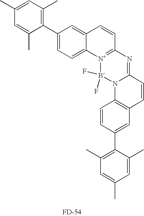
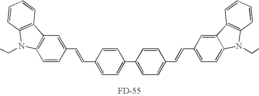


- Preferred fluorescent blue dopants may be found in Chen, Shi, and Tang, “Recent Developments in Molecular Organic Electroluminescent Materials,” Macromol. Symp. 125, 1 (1997) and the references cited therein; Hung and Chen, “Recent Progress of Molecular Organic Electroluminescent Materials and Devices,” Mat. Sci. and Eng. R39, 143 (2002) and the references cited therein. It should be noted that FD-46 and FD-49 are fluoranthene derivatives with annulated rings.
- A particularly preferred class of blue-emitting fluorescent dopants is represented by Formula (N), known as a bis(azinyl)amine borane complex, and is described in U.S. Pat. No. 6,661,023.
-

- wherein:
-
- A and A′ represent independent azine ring systems corresponding to 6-membered aromatic ring systems containing at least one nitrogen;
- each Xa and Xb is an independently selected substituent, two of which may join to form a fused ring to A or A′;
- m and n are independently 0 to 4;
- Za and Zb are independently selected substituents; and
- 1, 2, 3, 4, 1′, 2′, 3′, and 4′ are independently selected as either carbon or nitrogen atoms.
- Desirably, the azine rings are either quinolinyl or isoquinolinyl rings such that 1, 2, 3, 4, 1′, 2′, 3′, and 4′ are all carbon; m and n are equal to or greater than 2; and Xa and Xb represent at least two carbon substituents which join to form an aromatic ring. Desirably, Za and Zb are fluorine atoms.
- Preferred embodiments further include devices where the two fused ring systems are quinoline or isoquinoline systems; the aryl or heterocyclic substituent is a phenyl group; there are present at least two Xa groups and two Xb groups which join to form a 6-6 fused ring, the fused ring systems are fused at the 1-2, 3-4, 1′-2′, or 3′-4′ positions, respectively, one or both of the fused rings is substituted by a phenyl group; and where the dopant is depicted in Formulae (N-a), (N-b), or (N-c).
-

- wherein:
-
- each Xc, Xd, Xe, Xf, Xg, and Xh is hydrogen or an independently selected substituent, one of which must be an aryl or heterocyclic group.
- Desirably, the azine rings are either quinolinyl or isoquinolinyl rings such that 1, 2, 3, 4, 1′, 2′, 3′, and 4′ are all carbon; m and n are equal to or greater than 2; and Xa and Xb represent at least two carbon substituents which join to form an aromatic ring, and one is an aryl or substituted aryl group. Desirably, Za and Zb are fluorine atoms.
- Of these, compound FD-54 is particularly useful.
- Coumarins represent a useful class of green-emitting dopants as described by Tang et al. in U.S. Pat. Nos. 4,769,292 and 6,020,078. Green dopants or light-emitting materials can be coated as 0.01 to 50% by weight into the host material, but typically coated as 0.01 to 30% and more typically coated as 0.01 to 15% by weight into the host material. Examples of useful green-emitting coumarins include C545T and C545TB. Quinacridones represent another useful class of green-emitting dopants. Useful quinacridones are described in U.S. Pat. No. 5,593,788, publication JP 09-13026A, and commonly assigned U.S. patent application Ser. No. 10/184,356 filed Jun. 27, 2002 by Lelia Cosimbescu, entitled “Device Containing Green Organic Light-Emitting Diode” the disclosure of which is incorporated herein.
- Examples of particularly useful green-emitting quinacridones are FD-7 and FD-8.
- Formula (N-d) below represents another class of green-emitting dopants useful in the invention.
-

- wherein:
-
- A and A′ represent independent azine ring systems corresponding to 6-membered aromatic ring systems containing at least one nitrogen;
- each Xa and Xb is an independently selected substituent, two of which may join to form a fused ring to A or A′;
- m and n are independently 0 to 4;
- Y is H or a substituent;
- Za and Zb are independently selected substituents; and
- 1, 2, 3, 4, 1′, 2′, 3′, and 4′ are independently selected as either carbon or nitrogen atoms.
- In the device, 1, 2, 3, 4, 1′, 2′, 3′, and 4′ are conveniently all carbon atoms. The device may desirably contain at least one or both of ring A or A′ that contains substituents joined to form a fused ring. In one useful embodiment there is present at least one Xa or Xb group selected from the group consisting of halide and alkyl, aryl, alkoxy, and aryloxy groups. In another embodiment, there is present a Za and Zb group independently selected from the group consisting of fluorine and alkyl, aryl, alkoxy and aryloxy groups. A desirable embodiment is where Za and Zb are F. Y is suitably hydrogen or a substituent such as an alkyl, aryl, or heterocyclic group.
- The emission wavelength of these compounds may be adjusted to some extent by appropriate substitution around the central bis(azinyl)methene boron group to meet a color aim, namely green. Some examples of useful material are FD-50, FD-51 and FD-52.
- Naphthacenes and derivatives thereof also represent a useful class of emitting dopants, which can also be used as stabilizers. These dopant materials can be coated as 0.01 to 50% by weight into the host material, but typically coated as 0.01 to 30% and more typically coated as 0.01 to 15% by weight into the host material. Naphthacene derivative YD-1 (t-BuDPN) below, is an example of a dopant material used as a stabilizer.
-

- Some examples of this class of materials are also suitable as host materials as well as dopants. For example, see U.S. Pat. No. 6,773,832 or U.S. Pat. No. 6,720,092. A specific example of this would be rubrene (FD-5).
- Another class of useful dopants are perylene derivatives; for example see U.S. Pat. No. 6,689,493. A specific examples is FD-46.
- Metal complexes of 8-hydroxyquinoline and similar derivatives (Formula O) constitute one class of useful non-electroluminescent host compounds capable of supporting electroluminescence, and are particularly suitable for light emission of wavelengths longer than 500 nm, e.g., green, yellow, orange, and red.
-

- wherein:
-
- M represents a metal;
- n is an integer of from 1 to 4; and
- Z independently in each occurrence represents the atoms completing a nucleus having at least two fused aromatic rings.
- From the foregoing it is apparent that the metal can be monovalent, divalent, trivalent, or tetravalent metal. The metal can, for example, be an alkali metal, such as lithium, sodium, or potassium; an alkaline earth metal, such as magnesium or calcium; an earth metal, such as aluminum or gallium, or a transition metal such as zinc or zirconium. Generally any monovalent, divalent, trivalent, or tetravalent metal known to be a useful chelating metal can be employed.
- Z completes a heterocyclic nucleus containing at least two fused aromatic rings, at least one of which is an azole or azine ring. Additional rings, including both aliphatic and aromatic rings, can be fused with the two required rings, if required. To avoid adding molecular bulk without improving on function the number of ring atoms is usually maintained at 18 or less.
- Illustrative of useful chelated oxinoid compounds are the following:
-
- O-1: Aluminum trisoxine[alias, tris(8-quinolinolato)aluminum(III)]
- O-2: Magnesium bisoxine[alias, bis(8-quinolinolato)magnesium(II)]
- O-3: Bis[benzo{f}-8-quinolinolato]zinc (II)
- O-4: Bis(2-methyl-8-quinolinolato)aluminum(III)-μ-oxo-bis(2-methyl-8-quinolinolato)aluminum(III)
- O-5: Indium trisoxine[alias, tris(8-quinolinolato)indium]
- O-6: Aluminum tris(5-methyloxine)[alias, tris(5-methyl-8-quinolinolato)aluminum(III)]
- O-7: Lithium oxine[alias, (8-quinolinolato)lithium(I)]
- O-8: Gallium oxine[alias, tris(8-quinolinolato)gallium(III)]
- O-9: Zirconium oxine[alias, tetra(8-quinolinolato)zirconium(IV)]
- O-10: Bis(2-methyl-8-quinolinato)-4-phenylphenolatoaluminum(III)
- Anthracene derivatives according to formula (P) are also very useful host materials in the LEL:
-

- wherein:
-
- R1-R10 are independently chosen from hydrogen, alkyl groups from 1-24 carbon atoms or aromatic groups from 1-24 carbon atoms. Particularly preferred are compounds where R1 and R6 are phenyl, biphenyl or napthyl, R3 is phenyl, substituted phenyl or napthyl and R2, R4, R5, R7-R10 are all hydrogen. Such anthracene hosts are known to have excellent electron transporting properties.
- Particularly desirable are derivatives of 9,10-di-(2-naphthyl)anthracene. Illustrative examples include 9,10-di-(2-naphthyl)anthracene (ADN) and 2-t-butyl-9,10-di-(2-naphthyl)anthracene (TBADN). Other anthracene derivatives can be useful as a non-electroluminescent compound in the LEL, such as diphenylanthracene and its derivatives, as described in U.S. Pat. No. 5,927,247. Styrylarylene derivatives as described in U.S. Pat. No. 5,121,029 and JP 08333569 are also useful non-electroluminescent materials. For example, 9,10-bis[4-(2,2-diphenylethenyl)phenyl]anthracene, 4,4′-Bis(2,2-diphenylethenyl)-1,1′-biphenyl (DPVBi) and phenylanthracene derivatives as described in EP 681,019 are useful non-electroluminescent materials.
- Some illustrative examples of suitable anthracenes are:
-


- Spacer layers, when present, are located in direct contact to a LEL. They may be located on either the anode or cathode side, or even both sides of the LEL. They typically do not contain any light-emissive dopants. One or more materials may be used and could be either a hole-transporting material as defined above or an electron-transporting material as defined below. If located next to a phosphorescent LEL, the material in the spacer layer should have higher triplet energy than that of the phosphorescent dopant in the LEL. Most desirably, the material in the spacer layer will be the same as used as the host in the adjacent LEL. Thus, any of the host materials described as also suitable for use in a spacer layer. The spacer layer should be thin; at least 0.1 nm, but preferably in the range of from 1.0 nm to 20 nm.
- When a LEL containing a phosphorescent emitter is present, it is desirable to locate a hole-
blocking layer 135 between the electron-transportinglayer 136 and the light-emittinglayer 134 to help confine the excitons and recombination events to the LEL. In this case, there should be an energy barrier for hole migration from co-hosts into the hole-blocking layer, while electrons should pass readily from the hole-blocking layer into the light-emitting layer comprising co-host materials and a phosphorescent emitter. It is further desirable that the triplet energy of the hole-blocking material be greater than that of the phosphorescent material. Suitable hole-blocking materials are described in WO 00/70655A2, WO 01/41512 and WO 01/93642 A1. Two examples of useful hole-blocking materials are bathocuproine (BCP) and bis(2-methyl-8-quinolinolato)(4-phenylphenolato)aluminum(III) (BAlq). Metal complexes other than BAlq are also known to block holes and excitons as described in US 20030068528. When a hole-blocking layer is used, its thickness can be between 2 and 100 nm and suitably between 5 and 10 nm. - The purpose of an electron-transporting layer is to allow efficient movement of electrons from the cathode to the LEL. As such, it does not emit substantial amounts of light.
- In one embodiment, the electron-transporting
layer 136 may be composed only of the fluoranthene derivative or may be a mixture of the fluoranthene with other appropriate materials. The % volume ratio of fluoranthene to additional material can be anywhere from 1% to 99%, more suitably at least 10% and typically, at least 30%. The fluoranthene or any additional materials used may be the same or different than used as in the LEL. If an organic lithium EIM is present, it may be the same or different as used in the EIL. - The anthracene class of electron-transporting materials can also be used in the ETL with or without the fluoranthene of the invention. These anthracene electron transporting derivatives are represented by Formula (P) as described above in connection with host materials for a LEL. The anthracene in the ETL can be the same or different from that used in the LEL.
- In addition to any of the electron-transporting materials previously described, any other materials known to be suitable for use in the ETL may be used. Included are, but are not limited to, chelated oxinoid compounds, anthracene derivatives, pyridine-based materials, imidazoles, oxazoles, thiazoles and their derivatives, polybenzobisazoles, cyano-containing polymers and perfluorinated materials. Other electron-transporting materials include various butadiene derivatives as disclosed in U.S. Pat. No. 4,356,429 and various heterocyclic optical brighteners as described in U.S. Pat. No. 4,539,507.
- A preferred class of benzazoles is described by Shi et al. in U.S. Pat. Nos. 5,645,948 and 5,766,779. Such compounds are represented by structural formula (Q):
-

-
- In formula (Q), n is selected from 2 to 8 and i is selected from 1-5;
- Z is independently O, NR or S;
- R is individually hydrogen; alkyl of from 1 to 24 carbon atoms, for example, propyl, t-butyl, heptyl, and the like; aryl or hetero-atom substituted aryl of from 5 to 20 carbon atoms, for example, phenyl and naphthyl, furyl, thienyl, pyridyl, quinolinyl and other heterocyclic systems; or halo such as chloro, fluoro; or atoms necessary to complete a fused aromatic ring; and
- X is a linkage unit consisting of carbon, alkyl, aryl, substituted alkyl, or substituted aryl, which conjugately or unconjugately connects the multiple benzazoles together.
- An example of a useful benzazole is 2,2′,2″-(1,3,5-phenylene)tris[1-phenyl-1H-benzimidazole] (TPBI) represented by a formula (Q-1) shown below:
-

- Another suitable class of the electron-transporting materials includes various substituted phenanthrolines as represented by formula (R):
-

-
- In formula (R), R1-R8 are independently hydrogen, alkyl group, aryl or substituted aryl group, and at least one of R1-R8 is aryl group or substituted aryl group.
- Examples of suitable materials are 2,9-dimethyl-4,7-diphenylphenanthroline (BCP) (see formula (R-1)) and 4,7-diphenyl-1,10-phenanthroline (Bphen) (see formula (R-2)).
-

- Suitable triarylboranes that function as an electron-transporting material may be selected from compounds having the chemical formula (S):
-

- wherein:
-
- Ar1 to Ar3 are independently an aromatic hydrocarbocyclic group or an aromatic heterocyclic group which may have a substituent. It is preferable that compounds having the above structure are selected from formula (S-1):
-

- wherein:
-
- R1-R15 are independently hydrogen, fluoro, cyano, trifluoromethyl, sulfonyl, alkyl, aryl or substituted aryl group.
- Specific representative embodiments of the triarylboranes include:
-

- The electron-transporting material may also be selected from substituted 1,3,4-oxadiazoles of formula (T):
-

- wherein:
-
- R1 and R2 are individually hydrogen; alkyl of from 1 to 24 carbon atoms, for example, propyl, t-butyl, heptyl, and the like; aryl or hetero-atom substituted aryl of from 5 to 20 carbon atoms, for example, phenyl and naphthyl, furyl, thienyl, pyridyl, quinolinyl and other heterocyclic systems; or halo such as chloro, fluoro; or atoms necessary to complete a fused aromatic ring.
- Illustrative of the useful substituted oxadiazoles are the following:
-

- The electron-transporting material may also be selected from substituted 1,2,4-triazoles according to formula (U):
-

- wherein:
-
- R1, R2 and R3 are independently hydrogen, alkyl group, aryl or substituted aryl group, and at least one of R1-R3 is aryl group or substituted aryl group. An example of a useful triazole is 3-phenyl-4-(1-naphtyl)-5-phenyl-1,2,4-triazole represented by formula (U-1):
-

- The electron-transporting material may also be selected from substituted 1,3,5-triazines. Examples of suitable materials are:
-
- 2,4,6-tris(diphenylamino)-1,3,5-triazine;
- 2,4,6-tricarbazolo-1,3,5-triazine;
- 2,4,6-tris(N-phenyl-2-naphthylamino)-1,3,5-triazine;
- 2,4,6-tris(N-phenyl-1-naphthylamino)-1,3,5-triazine;
- 4,4′,6,6′-tetraphenyl-2,2′-bi-1,3,5-triazine;
- 2,4,6-tris([1,1′:3′,1″-terphenyl]-5′-yl)-1,3,5-triazine.
- In addition, any of the metal chelated oxinoid compounds including chelates of oxine itself (also commonly referred to as 8-quinolinol or 8-hydroxyquinoline) of Formula (O) useful as host materials in a LEL are also suitable for use in the ETL.
- Some metal chelated oxinoid compounds having high triplet energy can be particularly useful as an electron-transporting materials. Particularly useful aluminum or gallium complex host materials with high triplet energy levels are represented by Formula (V).
-

- In Formula (V), M1 represents Al or Ga. R2-R7 represent hydrogen or an independently selected substituent. Desirably, R2 represents an electron-donating group. Suitably, R3 and R4 each independently represent hydrogen or an electron donating substituent. A preferred electron-donating group is alkyl such as methyl. Preferably, R5, R6, and R7 each independently represent hydrogen or an electron-accepting group. Adjacent substituents, R2-R7, may combine to form a ring group. L is an aromatic moiety linked to the aluminum by oxygen, which may be substituted with substituent groups such that L has from 6 to 30 carbon atoms.
- IIlustrative of useful chelated oxinoid compounds for use in the ETL is Aluminum(III)bis(2-methyl-8-hydroxyquinoline)-4-phenylphenolate[alias, Balq].
- The same anthracene derivatives according to formula (P) useful as host materials in the LEL can also be used in the ETL.
- The thickness of the ETL is in the range of from 5 nm to 200 nm, preferably, in the range of from 10 nm to 150 nm.
- The organic lithium compound of the invention is typically located in the
EIL 138. The EIL may be composed only of the organic lithium compound, which is preferred, or there may be other materials present. For example, the EIL may be an n-type doped layer containing at least one electron-transporting material as a host and at least one n-type dopant. The dopant is capable of reducing the host by charge transfer. The term “n-type doped layer” means that this layer has semiconducting properties after doping, and the electrical current through this layer is substantially carried by the electrons. - The host in the EIL may be an electron-transporting material capable of supporting electron injection and electron transport. The electron-transporting material can be selected from the electron-transporting materials for use in the ETL region as defined above.
- The n-type dopant in the n-type doped EIL may be is selected from alkali metals, alkali metal compounds, alkaline earth metals, or alkaline earth metal compounds, or combinations thereof. The term “metal compounds” includes organometallic complexes, metal-organic salts, and inorganic salts, oxides and halides. Among the class of metal-containing n-type dopants, Li, Na, K, Rb, Cs, Mg, Ca, Sr, Ba, La, Ce, Sm, Eu, Tb, Dy, or Yb, and their compounds, are particularly useful. The materials used as the n-type dopants in the n-type doped EIL also include organic reducing agents with strong electron-donating properties. By “strong electron-donating properties” it is meant that the organic dopant should be able to donate at least some electronic charge to the host to form a charge-transfer complex with the host. Nonlimiting examples of organic molecules include bis(ethylenedithio)-tetrathiafulvalene (BEDT-TTF), tetrathiafulvalene (TTF), and their derivatives. In the case of polymeric hosts, the dopant is any of the above or also a material molecularly dispersed or copolymerized with the host as a minor component. Preferably, the n-type dopant in the n-type doped EIL includes Li, Na, K, Rb, Cs, Mg, Ca, Sr, Ba, La, Ce, Nd, Sm, Eu, Tb, Dy, or Yb, or combinations thereof The n-type doped concentration is preferably in the range of 0.01-20% by volume of this layer.
- When the EIL is composed only of the organic lithium compound of the invention, the thickness of the EIL is typically less than 20 nm, and preferably in the range of less than 5 nm. When an n-type doped EIL is employed, the thickness is typically less than 200 nm, and preferably in the range of less than 150 nm.
- When light emission is viewed solely through the anode, the
cathode 140 includes nearly any conductive material. Desirable materials have effective film-forming properties to ensure effective contact with the underlying organic layer, promote electron injection at low voltage, and have effective stability. Useful cathode materials often contain a low work function metal (<4.0 eV) or metal alloy. One preferred cathode material includes a Mg:Ag alloy as described in U.S. Pat. No. 4,885,221. Another suitable class of cathode materials includes bilayers including a thin inorganic EIL in contact with an organic layer (e.g., organic EIL or ETL), which is capped with a thicker layer of a conductive metal. Here, the inorganic EIL preferably includes a low work function metal or metal salt and, if so, the thicker capping layer does not need to have a low work function. One such cathode includes a thin layer of LiF followed by a thicker layer of A1 as described in U.S. Pat. No. 5,677,572. Other useful cathode material sets include, but are not limited to, those disclosed in U.S. Pat. Nos. 5,059,861, 5,059,862, and 6,140,763. - When light emission is viewed through the cathode,
cathode 140 should be transparent or nearly transparent. For such applications, metals should be thin or one should use transparent conductive oxides, or include these materials. Optically transparent cathodes have been described in more detail in U.S. Pat. Nos. 4,885,211, 5,247,190, 5,703,436, 5,608,287, 5,837,391, 5,677,572, 5,776,622, 5,776,623, 5,714,838, 5,969,474, 5,739,545, 5,981,306, 6,137,223, 6,140,763, 6,172,459, 6,278,236, 6,284,393, and EP 1 076 368. Cathode materials are typically deposited by thermal evaporation, electron beam evaporation, ion sputtering, or chemical vapor deposition. When needed, patterning is achieved through many well known methods including, but not limited to, through-mask deposition, integral shadow masking, for example as described in U.S. Pat. No. 5,276,380 and EP 0 732 868, laser ablation, and selective chemical vapor deposition. -
OLED 100 is typically provided over a supportingsubstrate 110 where either theanode 120 orcathode 140 can be in contact with the substrate. The electrode in contact with the substrate is conveniently referred to as the bottom electrode. Conventionally, the bottom electrode is theanode 120, but this invention is not limited to that configuration. The substrate can either be light transmissive or opaque, depending on the intended direction of light emission. The light transmissive property is desirable for viewing the EL emission through the substrate. Transparent glass or plastic is commonly employed in such cases. The substrate can be a complex structure comprising multiple layers of materials. This is typically the case for active matrix substrates wherein TFTs are provided below the OLED layers. It is still necessary that the substrate, at least in the emissive pixelated areas, be comprised of largely transparent materials such as glass or polymers. For applications where the EL emission is viewed through the top electrode, the transmissive characteristic of the bottom support is immaterial, and therefore the substrate can be light transmissive, light absorbing or light reflective. Substrates for use in this case include, but are not limited to, glass, plastic, semiconductor materials such as silicon, ceramics, and circuit board materials. Again, the substrate can be a complex structure comprising multiple layers of materials such as found in active matrix TFT designs. It is necessary to provide in these device configurations a light-transparent top electrode. - The organic materials mentioned above are suitably deposited through sublimation, but can be deposited from a solvent with an optional binder to improve film formation. If the material is a polymer, solvent deposition is usually preferred. The material to be deposited by sublimation can be vaporized from a sublimator “boat” often comprised of a tantalum material, e.g., as described in U.S. Pat. No. 6,237,529, or can be first coated onto a donor sheet and then sublimed in closer proximity to the substrate. Layers with a mixture of materials can utilize separate sublimator boats or the materials can be premixed and coated from a single boat or donor sheet. Patterned deposition can be achieved using shadow masks, integral shadow masks (U.S. Pat. No. 5,294,870), spatially-defined thermal dye transfer from a donor sheet (U.S. Pat. No. 5,851,709 and U.S. Pat. No. 6,066,357) and inkjet method (U.S. Pat. No. 6,066,357).
- Organic materials useful in making OLEDs, for example organic hole-transporting materials, organic light-emitting materials doped with an organic electroluminescent components have relatively complex molecular structures with relatively weak molecular bonding forces, so that care must be taken to avoid decomposition of the organic material(s) during physical vapor deposition. The aforementioned organic materials are synthesized to a relatively high degree of purity, and are provided in the form of powders, flakes, or granules. Such powders or flakes have been used heretofore for placement into a physical vapor deposition source wherein heat is applied for forming a vapor by sublimation or vaporization of the organic material, the vapor condensing on a substrate to provide an organic layer thereon.
- Several problems have been observed in using organic powders, flakes, or granules in physical vapor deposition: These powders, flakes, or granules are difficult to handle. These organic materials generally have a relatively low physical density and undesirably low thermal conductivity, particularly when placed in a physical vapor deposition source which is disposed in a chamber evacuated to a reduced pressure as low as 10−6 Torr. Consequently, powder particles, flakes, or granules are heated only by radiative heating from a heated source, and by conductive heating of particles or flakes directly in contact with heated surfaces of the source. Powder particles, flakes, or granules which are not in contact with heated surfaces of the source are not effectively heated by conductive heating due to a relatively low particle-to-particle contact area; This can lead to nonuniform heating of such organic materials in physical vapor deposition sources. Therefore, result in potentially nonuniform vapor-deposited organic layers formed on a substrate.
- These organic powders can be consolidated into a solid pellet. These solid pellets consolidating into a solid pellet from a mixture of a sublimable organic material powder are easier to handle. Consolidation of organic powder into a solid pellet can be accomplished with relatively simple tools. A solid pellet formed from mixture comprising one or more non-luminescent organic non-electroluminescent component materials or luminescent electroluminescent component materials or mixture of non-electroluminescent component and electroluminescent component materials can be placed into a physical vapor deposition source for making organic layer. Such consolidated pellets can be used in a physical vapor deposition apparatus.
- In one aspect, the present invention provides a method of making an organic layer from compacted pellets of organic materials on a substrate, which will form part of an OLED.
- One preferred method for depositing the materials of the present invention is described in US 2004/0255857 and U.S. Ser. No. 10/945,941 where different source evaporators are used to evaporate each of the materials of the present invention. A second preferred method involves the use of flash evaporation where materials are metered along a material feed path in which the material feed path is temperature controlled. Such a preferred method is described in the following co-assigned patent applications: U.S. Ser. No. 10/784,585; U.S. Ser. No. 10/805,980; U.S. Ser. No. 10/945,940; U.S. Ser. No. 10/945,941; U.S. Ser. No. 11/050,924; and U.S. Ser. No. 11/050,934. Using this second method, each material may be evaporated using different source evaporators or the solid materials may be mixed prior to evaporation using the same source evaporator.
- Most OLED devices are sensitive to moisture and/or oxygen so they are commonly sealed in an inert atmosphere such as nitrogen or argon, along with a desiccant such as alumina, bauxite, calcium sulfate, clays, silica gel, zeolites, alkaline metal oxides, alkaline earth metal oxides, sulfates, or metal halides and perchlorates. Methods for encapsulation and desiccation include, but are not limited to, those described in U.S. Pat. No. 6,226,890.
- For full color display, the pixelation of LELs can be needed. This pixelated deposition of LELs is achieved using shadow masks, integral shadow masks, U.S. Pat. No. 5,294,870, spatially defined thermal dye transfer from a donor sheet, U.S. Pat. Nos. 5,688,551, 5,851,709, and 6,066,357, and inkjet method, U.S. Pat. No. 6,066,357.
- OLED devices of this invention can employ various well-known optical effects in order to enhance its properties if desired. This includes optimizing layer thicknesses to yield maximum light transmission, providing dielectric mirror structures, providing reflective layers or microcavity structures, replacing reflective electrodes with light-absorbing electrodes, providing anti-glare or anti-reflection coatings over the display, providing a polarizing medium over the display, or providing colored, neutral density, or color-conversion filters over the display. Filters, polarizers, and anti-glare or anti-reflection coatings may be specifically provided over the cover or as part of the cover.
- Embodiments of the invention may provide EL devices that have good luminance efficiency, good operational stability, and reduced drive voltages. Embodiments of the invention may also give reduced voltage rises over the lifetime of the devices and can be produced with high reproducibility and consistently to provide good light efficiency. They may have lower power consumption requirements and, when used with a battery, provide longer battery lifetimes.
- It should be understood that in the synthesis of organic molecules, particular synthetic pathways can give rise to molecules, either exclusively or as mixtures of molecules, which have the same molecular formulae but differ only in having a particular substituent located at a different site somewhere in the molecule. In other words, the molecules or the molecules in the mixtures may differ from each other by the arrangement of their substituents or more generally, the arrangement of some of their atoms in space. When this occurs, the materials are referred to as isomers. A broader definition of an isomer can be found in Grant and Hackh's Chemical Dictionary, Fifth Edition, McGraw-Hill Book Company, page 313. The synthetic pathway outlined for Example 2 is an example of a pathway that can give rise to isomers by virtue of how the acetylene molecule reacts spatially with the unsymmetrical framework of the 8H-cyclopent[a]acenaphthylen-8-one entity of the second molecule. In this particular example, two isomers are possible, ETM2 and ETM7. It should be realized that the current invention includes not only examples of molecules represented by generic Formulae I, II and III and their specific molecular examples, but also includes all the isomers associated with these structures. In addition, examples of compounds of the invention and their isomers are not limited to those derived from a symmetrical or unsymmetrical 8H-cyclopent[a]acenaphthylen-8-one framework, but can also include other frameworks and methods of preparation that are useful in producing compounds of Formulae I, II and III.
- Inventive Compound, ETM1 was synthesized as outlined in the following scheme:
-

- 7,9-Diphenyl-8H-Cyclopent[a]acenaphthylen-8-one, (aka Acecyclone), (1) was prepared according to the procedure of W. Dilthey, I ter Horst and W. Schommer; Journal fuer Praktische Chemie (Leipzig), 143, (1935), 189-210, in satisfactory yield.
- Acecyclone (12 g, 33.6 mMole) and 4-biphenylacetylene (9.0 g, 50.5 mMole) were heated to gentle reflux in ortho-dichlorobenzene (100 mL) for 2 hours. The reaction was then cooled, treated with methanol (20 mL) and stirred at room temperature for 1 hour. The resulting yellow solid was filtered of, washed well with methanol and dried. Yield of product ETM1, 17.4 g. Before use in device fabrication, ETM1 was sublimed at 220° C./10−3 mm Hg.
- The inventive compound ETM2 was synthesized as outlined in the following scheme:
-

- 5-Bromoacenaphthenequinone (2) was prepared according to the procedure of Gordon H. Rule and Samuel B. Thompson; Journal of the Chemical Society, (1937), 1761-1763, in satisfactory yield.
- 1,3-Diphenylacetone (17.5 g, 83 mMole) was dissolved in methanol (240 mL) and heated to 65° C. To the solution was added 5-bromoacenaphthenequinone (2), (20 g, 75 mMole). The resulting well-stirred suspension was then treated with 1M-methanolic KOH (100 ML, 100 mMole) at a fast drip rate, whereupon the dark colored product precipitated immediately. The mixture was then stirred at 65° C. for 1 hour, cooled and filtered. The black solid was washed well with methanol, ether and dried. Yield of product (3), (31 g).
- A mixture of 3-bromo-7,9-diphenyl-8H-Cyclopent[a]acenaphthylen-8-one, (20 g, 46 mMole) and 4-biphenylacetylene (12.3 g, 69 mMole) in ortho-dichlorobenzene (200 mL) were heated to gentle reflux for 2 hours. The resulting solution was cooled and treated with methanol (150 mL). During the course of 1 hour the product crystallized as a bright yellow solid. Yield of product (4), 22 g.
- A mixture of 3-bromo-8-[1,1′-biphenyl]-4-yl-7,10-diphenylfluoranthene (7.2 g, 12 mMole), tetrakis(triphenylphosphine)palladium(0) (0.44 g, 3-mol-% based on the fluoranthene) and phenylboronic acid (1.8 g, 14 mMole), were suspended in toluene (100 mL) and stirred well with a mechanical stirrer. To this was then added 2M-Na2CO3 (14 mL) followed by ethanol (20 mL) and the mixture heated to gentle reflux for 1 hour. This mixture was then cooled to room temperature and treated with methanol (100 mL). The yellow solid was filtered off, washed well with water, methanol and ether, and then dried. Yield of product ETM2, 5.1 g. Before use in device fabrication, ETM2 was sublimed at 260° C/10−3 mm Hg.
- A series of EL devices (3.1 through 3.8) were constructed in the following manner:
- 1. A glass substrate coated with an 85 nm layer of indium-tin oxide (ITO), as the anode, was sequentially ultrasonicated in a commercial detergent, rinsed in deionized water, and exposed to oxygen plasma for about 1 min.
- 2. Over the ITO was deposited a 1 nm fluorocarbon (CFx) hole-injecting layer (HIL) by plasma-assisted deposition of CHF3 as described in U.S. Pat. No. 6,208,075.
- 3. Next a layer of hole-transporting material 4,4′-Bis[N-(1-naphthyl)-N-phenylamino]biphenyl (NPB) was deposited to a thickness of 95 nm.
- 4. A 20 nm light-emitting layer (LEL) composed of host material P-4, 1.5% of light emitting dopant FD-54, and the non-light emitting co-host ETM2, as recorded in Table 1, was then deposited.
- 5. A 35 nm electron-transporting layer (ETL) with ETM2, as shown in Table 1, was vacuum-deposited over the LEL.
- 6. An electron-injecting layer (EIL) as shown in Table 1, was vacuum deposited onto the ETL.
- 7. And finally, a 100 nm layer of aluminum was deposited onto the EIL, to form the cathode.
- The above sequence completes the deposition of the EL devices. The devices were then hermetically packaged in a dry glove box for protection against ambient environment. The devices thus formed were tested for luminous efficiency at an operating current of 20 mA/cm2 and the results are reported in Table 1.
-
TABLE 1 

Experimental Results Drive Example Volt. Efficiency (Type) LEL ETL EIL (Volts) (cd/A) 3.1 P-4 + Comp-1 EIM1 7.7 2.2 (Comparative) 1.5% FD-54 3.2 P-4 + Comp-1 EIM1 7.7 2.5 (Comparative) +2% Comp-1 +1.5% FD-54 3.3 P-4 + Comp-1 EIM1 7.6 2.4 (Comparative) +5% Comp-1 +1.5% FD-54 3.4 P-4 + Comp-1 EIM1 7.6 2.1 (Comparative) +10% Comp-1 +1.5% FD-54 3.5 P-4 + Comp-1 EIM1 6.7 1.8 (Comparative) +30% Comp-1 +1.5% FD-54 3.6 P-4 + ETM2 EIM1 5.1 5.6 (Comparative 1.5% FD-54 3.7 P-4 ETM2 EIM1 4.8 6.6 (Inventive) +2% ETM2 +1.5% FD-54 3.8 P-4 + ETM2 EIM1 5.3 7.5 (Inventive) +5% ETM2 +1.5% FD-54 3.9 P-4 + ETM2 EIM1 4.7 7.2 (Inventive) +10% ETM2 +1.5% FD-54 3.10 P-4 + ETM2 EIM1 4.3 7.4 (Inventive) +30% ETM2 +1.5% FD-54 - Devices 3.1 to 3.5 of Table 1 are for comparative purposes and contain Comp-1 in the ETL. Device 3.1 contains no co-host in the LEL but P-4 as the only host. In devices 3.2 to 3.5 there are various volume % measures of the non-light emitting co-host Comp-1 in the LEL. Comp-1 is a material that falls outside the scope of the current invention. Device 3.6 is also a comparative device. It contains ETM2 in the ETL and P-4 as the only host in the LEL. Devices 3.7 to 3.10 are inventive and have ETM2 as a co-host in the LEL. The levels of ETM2 in the LEL are the same as the levels in the comparison devices 3.2 to 3.5. The organolithium complex as required by the invention, is present in both the comparative and inventive devices. From the table it can be seen that the performance of the inventive devices in terms of desirably higher luminance and lower drive voltage, is far superior to the comparison devices, at all levels of ETM2. In fact, when there is no co-host present in the LEL but P-4 alone, as shown in comparative device 3.6, inferior performance compared to those devices with the co-host is observed.
- A series of EL devices (4.1 through 4.4) were constructed in the following manner:
- 1. A glass substrate coated with an 85 nm layer of indium-tin oxide (ITO), as the anode, was sequentially ultrasonicated in a commercial detergent, rinsed in deionized water, and exposed to oxygen plasma for about 1 min.
- 2. Over the ITO was deposited a 1 nm fluorocarbon (CFx) hole-injecting layer (HIL) by plasma-assisted deposition of CHF3 as described in U.S. Pat. No. 6,208,075.
- 3. Next a layer of hole-transporting material 4,4′-Bis[N-(1-naphthyl)-N-phenylamino]biphenyl (NPB) was deposited to a thickness of 144 nm.
- 4. A 40 nm light-emitting layer (LEL) composed of host material FD-5, 0.5% of light emitting dopant FD-46, and the non-light emitting co-host ETM2, as recorded in Table 2, was then deposited.
- 5. A 35 nm electron-transporting layer (ETL) of ETM2, was vacuum-deposited over the LEL.
- 6. A 35 nm electron-injecting layer (EIL) of EIM1, was vacuum deposited onto the ETL.
- 7. And finally, a 100 nm layer of aluminum was deposited onto the EIL, to form the cathode.
- The above sequence completes the deposition of the EL devices. The devices were then hermetically packaged in a dry glove box for protection against ambient environment. The devices thus formed were tested for luminous efficiency at an operating current of 20 mA/cm2 and the results are reported in Tables 2 and 3.
-
TABLE 2 Experimental Results Example Drive Volt. Efficiency (Type) LEL ETL EIL (Volts) (cd/A) CIEx,y 4.1 FD-5 + 0.5% ETM2 EIM1 5.5 10.4 0.65, 0.34 (Comparative) FD-46 4.2 FD-5 + 10% ETM2 EIM1 4.8 12.2 0.66, 0.34 (Inventive) ETM2 + 0.5% FD-46 4.3 FD-5 + 20% ETM2 EIM1 4.6 11.5 0.65, 0.35 (Inventive) ETM2 + 0.5% FD-46 4.4 FD-5 + 50% ETM2 EIM1 4.9 11.8 0.66, 0.34 (Inventive) ETM2 + 0.5% FD-46 - Device 4.1 is a comparative device that is the same in all aspects to the inventive devices 4.2 to 4.4, except that device 4.1 has no ETM2 in the LEL and as such falls outside the scope of the current invention. It is clear from Table 2 that when ETM2 is in both the LEL and ETL with an organolithium complex as the EIM, the devices give better performance in terms of higher luminance efficiency and lower drive voltage. In addition to improvements in luminance and voltage performances, addition of co-host materials in the LEL also leads to improvements in fade stability. Table 3 shows the time in hours, it takes to reach a luminance efficiency of 50% of the original value when the devices are subjected to a current density of 80 mA/cm2: the longer the device takes to reach the T50 value, the more desirable it is. As can be seen from Table 3, the inventive devices 4.2 to 4.4 give greatly improved fade performance over the comparative device with no ETM2 in the LEL. As can be readily seen in
FIG. 2 and the CIEx,y data, the addition of ETM2 causes no change in the emission spectra nor any emission in the blue region, thus indicating that ETM2 does not substantially emit light. -
TABLE 3 Experimental Fade Results Example T50 @ 80 mA/cm2 (Type) (hours) 4.1 190 (Comparative) 4.2 225 (Inventive) 4.3 490 (Inventive) 4.4 1506 (Inventive) - A series of EL devices (5.1 through 5.5) was constructed in a similar manner to Example 4, except that EIM2 was used in place of EIM1 in the EIL layer of step 6. The results are reported in Table 4.
-
TABLE 4 Experimental Results Example Drive Volt. Efficiency (Type) LEL ETL EIL (Volts) (cd/A) CIEx,y 5.1 FD-5 + 0.5% ETM2 EIM2 6.3 7.3 0.66, 0.34 (Comparative) FD-46 5.2 FD-5 + 10% ETM2 EIM2 6.6 9.2 0.66, 0.34 (Inventive) ETM2 + 0.5% FD-46 5.3 FD-5 + 20% ETM2 EIM2 6.5 10.6 0.66, 0.34 (Inventive) ETM2 + 0.5% FD-46 5.4 FD-5 + 50% ETM2 EIM2 6.4 11.6 0.66, 0.34 (Inventive) ETM2 + 0.5% FD-46 5.5 FD-5 + 70% ETM2 EIM2 6.7 8.4 0.66, 0.34 (Inventive) ETM2 + 0.5% FD-46 - Device 5.1, which has no ETM2 in the LEL, is a comparative example. Devices 5.2 through 5.5 are inventive devices and are identical to 5.1 except that ETM2 is incorporated into the LEL of the inventive devices. From Table 4 it can be seen that the inventive devices give better luminance efficiency than the comparative device. As can be readily seen in
FIG. 3 and the CIEx,y data, the addition of ETM2 causes no change in the emission spectra nor any emission in the blue region, thus indicating that ETM2 does not substantially emit light. - A series of EL devices (6.1 through 6.4) was constructed in a similar manner to Example 4, except that ETM1 was used in place of ETM2 in both the LEL and ETL of steps 4 and 5. The results are reported in Table 5.
-
TABLE 5 Experimental Results Example Drive Volt. Efficiency (Type) LEL ETL EIL (Volts) (cd/A) CIEx,y 6.1 FD-5 + 0.5% ETM21 EIM1 5.6 9.1 0.66, 0.34 (Comparative) FD-46 6.2 FD-5 + 10% ETM21 EIM1 5.4 10.6 0.66, 0.34 (Inventive) ETM21 + 0.5% FD-46 6.3 FD-5 + 20% ETM21 EIM1 5.4 11.4 0.66, 0.34 (Inventive) ETM21 + 0.5% FD-46 6.4 FD-5 + 50% ETM21 EIM1 5.6 10.5 0.66, 0.34 (Inventive) ETM21 + 0.5% FD-46 - Device 6.1 has no ETM21 in the LEL and is a comparative example. Devices 6.2 through 6.4 are inventive devices and are identical to 6.1 except that co-host ETM21 is incorporated into the LEL of the inventive devices. From Table 5 it can be seen that the inventive devices give better luminance efficiency than the comparative device. As can be readily seen in
FIG. 4 and the CIEx,y data, the addition of ETM2 causes no change in the emission spectra nor any emission in the blue region, thus indicating that ETM21 does not substantially emit light. - A series of EL devices (7.1 through 7.4) was constructed in a similar manner to Example 3, except that ETM21 was used in place of ETM2 in both the LEL and ETL of steps 4 and 5. The results are reported in Table 6.
-
TABLE 6 Experimental Results Example Drive Volt. Efficiency (Type) LEL ETL EIL (Volts) (cd/A) CIEx,y 7.1 P-4 + 1.5% ETM21 EIM1 5.1 6.7 0.14, 0.15 (Comparative) FD-54 7.2 P-4 + 5% ETM21 EIM1 5.1 6.9 0.14, 0.14 (Inventive) ETM21 + 1.5% FD-54 7.3 P-4 + 10% ETM21 EIM1 5.1 7.0 0.14, 0.14 (Inventive) ETM21 + 1.5% FD-54 7.4 P-4 + 30% ETM21 EIM1 4.9 7.3 0.14, 0.15 (Inventive) ETM21 + 1.5% FD-54 - Device 7.1 has no ETM21 in the LEL and is a comparative example. Devices 7.2 through 7.4 are inventive devices and are identical to 7.1 except that ETM21 is incorporated into the LEL of the inventive devices. From Table 6 it can be seen that the inventive devices give better luminance efficiency than the comparative device. As can be readily seen in
FIG. 5 and the CIEx,y data, the addition of ETM21 causes no change in the emission spectra, thus indicating that ETM2 does not substantially emit light. - A series of white EL devices (8.1 through 8.4) were constructed in the following manner:
- 1. A glass substrate coated with a 20 nm layer of indium-tin oxide (ITO), as the anode, was sequentially ultrasonicated in a commercial detergent, rinsed in deionized water and exposed to oxygen plasma for about 1 min.
- 2. Over the ITO was deposited a 10 nm hole-injecting layer (HIL) of dipyrazino[2,3-f:2′,3′-h]quinoxalinehexacarbonitrile.
- 3. Next a layer of hole-transporting material 4,4′-Bis[N-(1-naphthyl)-N-phenylamino]biphenyl (NPB) was deposited to a thickness of 65 nm.
- 4. A 20 nm yellow light-emitting layer (LEL1) of 69% NPB host, 30% P-2 host and 1% dopant FD-57 was then deposited.
- 5. A 20 nm blue light-emitting layer (LEL2) of 98.5% P-2 host and 1.5% FD-54 dopant was then deposited.
- 6. A 31.5 nm electron-transporting layer (ETL) of 75% P-1 and 25% EIM2 was vacuum-deposited over the LEL.
- 7. A 3.5 nm electron-injecting layer (EIL) of EIM1 was then vacuum deposited onto the ETL.
- 8. And finally, a 100 nm layer of aluminum was deposited onto the EIL, to form the cathode.
- The above sequence completes the deposition of the EL device 8.1. The device was then hermetically packaged in a dry glove box for protection against ambient environment.
- Device 8.2 was prepared as device 8.1 except LEL2 of step 5 was composed of 98.5% ETN as the host and 1.5% FD-54 as the dopant. Device 8.3 was the same as device 8.1 except that the ETL of step 6 was replaced with 100% ETM2. Device 8.4 was the same as device 8.1 except that the ETL of step 6 was replaced with 100% ETM2.
- The devices thus formed were tested for voltage and color at an operating current of 20 mA/cm2 and the results are reported in Table 10.
-
TABLE 10 Device Results Drive Example Volt. (Type) LEL2 ETL EIL (Volts) CIEx, y 8.1 P-2 + FD-54 P-1 + EIM2 EIM1 4.0 0.29, 0.28 (Comparative) 8.2 ETM2 + FD- P-1 + EIM2 EIM1 3.1 0.32, 0.35 (Inventive) 54 8.3 P-2 + FD-54 ETM2 EIM1 3.9 0.28, 0.27 (Comparative) 8.4 ETM2 + FD- ETM2 EIM1 3.3 0.34, 0.36 (Inventive) 54 - As seen in Table 10, the use of ETM-2 as a host in a blue light-emitting layer of a white OLED device lowers the voltage (device 8.2 versus 8.1). The additional use of ETM2 as the ETL layer (device 8.4 versus 8.3) further improves the voltage. The color emission of the devices with the inventive fluoranthenes are much closer to an ideal white (approximately 0.33, 0.33) than the check devices.
FIGS. 6 and 7 show the spectral response versus wavelength for these devices demonstrating the excellent white color due to an improved height ratio between the blue, green and red peaks. - The invention has been described in detail with particular reference to certain preferred embodiments thereof, but it will be understood that variations and modifications can be effected within the spirit and scope of the invention. The patents and other publications referred to are incorporated herein in their entirety.
-
- 100 OLED
- 110 Substrate
- 120 Anode
- 130 Hole-Injecting layer (HIL)
- 132 Hole-Transporting layer (HTL)
- 134 Light-Emitting layer (LEL)
- 135 Hole-Blocking Layer (HBL)
- 136 Electron-Transporting layer (ETL)
- 138 Electron-Injecting layer (EIL)
- 140 Cathode
- 150 Voltage/Current Source
- 160 Electrical Connectors
Claims (25)


(Li+)m(Q)n Formula (IV)


Priority Applications (1)
| Application Number | Priority Date | Filing Date | Title |
|---|---|---|---|
| US11/924,626 US8431242B2 (en) | 2007-10-26 | 2007-10-26 | OLED device with certain fluoranthene host |
Applications Claiming Priority (1)
| Application Number | Priority Date | Filing Date | Title |
|---|---|---|---|
| US11/924,626 US8431242B2 (en) | 2007-10-26 | 2007-10-26 | OLED device with certain fluoranthene host |
Publications (2)
| Publication Number | Publication Date |
|---|---|
| US20090110957A1 true US20090110957A1 (en) | 2009-04-30 |
| US8431242B2 US8431242B2 (en) | 2013-04-30 |
Family
ID=40583235
Family Applications (1)
| Application Number | Title | Priority Date | Filing Date |
|---|---|---|---|
| US11/924,626 Active 2031-02-12 US8431242B2 (en) | 2007-10-26 | 2007-10-26 | OLED device with certain fluoranthene host |
Country Status (1)
| Country | Link |
|---|---|
| US (1) | US8431242B2 (en) |
Cited By (8)
| Publication number | Priority date | Publication date | Assignee | Title |
|---|---|---|---|---|
| US20100176389A1 (en) * | 2009-01-13 | 2010-07-15 | Samsung Mobile Display Co., Ltd. | Organic light emitting diode and method of manufacturing the same |
| US20100253209A1 (en) * | 2009-04-03 | 2010-10-07 | Spindler Jeffrey P | Tandem white oled with efficient electron transfer |
| US8076009B2 (en) | 2007-10-26 | 2011-12-13 | Global Oled Technology, Llc. | OLED device with fluoranthene electron transport materials |
| US20120025225A1 (en) * | 2010-07-27 | 2012-02-02 | Seiko Epson Corporation | Light-emitting element, display device, and electronic apparatus |
| US8420229B2 (en) | 2007-10-26 | 2013-04-16 | Global OLED Technologies LLC | OLED device with certain fluoranthene light-emitting dopants |
| US20170186981A1 (en) * | 2015-12-28 | 2017-06-29 | Samsung Display Co., Ltd. | Organic light-emitting device |
| US20170194589A1 (en) * | 2015-08-28 | 2017-07-06 | Boe Technology Group Co., Ltd. | Organic light emitting device and method of fabricating the same, and display device |
| US20220158118A1 (en) * | 2020-11-17 | 2022-05-19 | Boe Technology Group Co., Ltd. | Light emitting device, display device and manufacturing method of light emitting device |
Citations (98)
| Publication number | Priority date | Publication date | Assignee | Title |
|---|---|---|---|---|
| US3173050A (en) * | 1962-09-19 | 1965-03-09 | Dow Chemical Co | Electroluminescent cell |
| US3172862A (en) * | 1960-09-29 | 1965-03-09 | Dow Chemical Co | Organic electroluminescent phosphors |
| US3180730A (en) * | 1959-04-09 | 1965-04-27 | Azoplate Corp | Material for electrophotographic purposes |
| US3567450A (en) * | 1968-02-20 | 1971-03-02 | Eastman Kodak Co | Photoconductive elements containing substituted triarylamine photoconductors |
| US3658520A (en) * | 1968-02-20 | 1972-04-25 | Eastman Kodak Co | Photoconductive elements containing as photoconductors triarylamines substituted by active hydrogen-containing groups |
| US3710167A (en) * | 1970-07-02 | 1973-01-09 | Rca Corp | Organic electroluminescent cells having a tunnel injection cathode |
| US4356429A (en) * | 1980-07-17 | 1982-10-26 | Eastman Kodak Company | Organic electroluminescent cell |
| US4539507A (en) * | 1983-03-25 | 1985-09-03 | Eastman Kodak Company | Organic electroluminescent devices having improved power conversion efficiencies |
| US4720432A (en) * | 1987-02-11 | 1988-01-19 | Eastman Kodak Company | Electroluminescent device with organic luminescent medium |
| US4768292A (en) * | 1985-05-22 | 1988-09-06 | Sevar Entsorgungsanlagen Gmbh | Method and apparatus for drying sewage sludge |
| US4769292A (en) * | 1987-03-02 | 1988-09-06 | Eastman Kodak Company | Electroluminescent device with modified thin film luminescent zone |
| US5059861A (en) * | 1990-07-26 | 1991-10-22 | Eastman Kodak Company | Organic electroluminescent device with stabilizing cathode capping layer |
| US5059862A (en) * | 1990-07-26 | 1991-10-22 | Eastman Kodak Company | Electroluminescent device with improved cathode |
| US5061569A (en) * | 1990-07-26 | 1991-10-29 | Eastman Kodak Company | Electroluminescent device with organic electroluminescent medium |
| US5121029A (en) * | 1987-12-11 | 1992-06-09 | Idemitsu Kosan Co., Ltd. | Electroluminescence device having an organic electroluminescent element |
| US5141671A (en) * | 1991-08-01 | 1992-08-25 | Eastman Kodak Company | Mixed ligand 8-quinolinolato aluminum chelate luminophors |
| US5150006A (en) * | 1991-08-01 | 1992-09-22 | Eastman Kodak Company | Blue emitting internal junction organic electroluminescent device (II) |
| US5151629A (en) * | 1991-08-01 | 1992-09-29 | Eastman Kodak Company | Blue emitting internal junction organic electroluminescent device (I) |
| US5247190A (en) * | 1989-04-20 | 1993-09-21 | Cambridge Research And Innovation Limited | Electroluminescent devices |
| US5276380A (en) * | 1991-12-30 | 1994-01-04 | Eastman Kodak Company | Organic electroluminescent image display device |
| US5294870A (en) * | 1991-12-30 | 1994-03-15 | Eastman Kodak Company | Organic electroluminescent multicolor image display device |
| US5405709A (en) * | 1993-09-13 | 1995-04-11 | Eastman Kodak Company | White light emitting internal junction organic electroluminescent device |
| US5406709A (en) * | 1992-05-08 | 1995-04-18 | Lawn Shark Inc. | Garden tool |
| US5409783A (en) * | 1994-02-24 | 1995-04-25 | Eastman Kodak Company | Red-emitting organic electroluminescent device |
| US5484922A (en) * | 1992-07-13 | 1996-01-16 | Eastman Kodak Company | Internal junction organic electroluminescent device with a novel composition |
| US5552678A (en) * | 1994-09-23 | 1996-09-03 | Eastman Kodak Company | AC drive scheme for organic led |
| US5554450A (en) * | 1995-03-08 | 1996-09-10 | Eastman Kodak Company | Organic electroluminescent devices with high thermal stability |
| US5593788A (en) * | 1996-04-25 | 1997-01-14 | Eastman Kodak Company | Organic electroluminescent devices with high operational stability |
| US5608287A (en) * | 1995-02-23 | 1997-03-04 | Eastman Kodak Company | Conductive electron injector for light-emitting diodes |
| US5645948A (en) * | 1996-08-20 | 1997-07-08 | Eastman Kodak Company | Blue organic electroluminescent devices |
| US5677572A (en) * | 1996-07-29 | 1997-10-14 | Eastman Kodak Company | Bilayer electrode on a n-type semiconductor |
| US5714838A (en) * | 1996-09-20 | 1998-02-03 | International Business Machines Corporation | Optically transparent diffusion barrier and top electrode in organic light emitting diode structures |
| US5739545A (en) * | 1997-02-04 | 1998-04-14 | International Business Machines Corporation | Organic light emitting diodes having transparent cathode structures |
| US5755999A (en) * | 1997-05-16 | 1998-05-26 | Eastman Kodak Company | Blue luminescent materials for organic electroluminescent devices |
| US5766779A (en) * | 1996-08-20 | 1998-06-16 | Eastman Kodak Company | Electron transporting materials for organic electroluminescent devices |
| US5776623A (en) * | 1996-07-29 | 1998-07-07 | Eastman Kodak Company | Transparent electron-injecting electrode for use in an electroluminescent device |
| US5776622A (en) * | 1996-07-29 | 1998-07-07 | Eastman Kodak Company | Bilayer eletron-injeting electrode for use in an electroluminescent device |
| US5908581A (en) * | 1997-04-07 | 1999-06-01 | Eastman Kodak Company | Red organic electroluminescent materials |
| US5927247A (en) * | 1996-09-26 | 1999-07-27 | Sanshin Kogyo Kabushiki Kaisha | Direct injected engine |
| US5928802A (en) * | 1997-05-16 | 1999-07-27 | Eastman Kodak Company | Efficient blue organic electroluminescent devices |
| US5935721A (en) * | 1998-03-20 | 1999-08-10 | Eastman Kodak Company | Organic electroluminescent elements for stable electroluminescent |
| US5935720A (en) * | 1997-04-07 | 1999-08-10 | Eastman Kodak Company | Red organic electroluminescent devices |
| US5969474A (en) * | 1996-10-24 | 1999-10-19 | Tdk Corporation | Organic light-emitting device with light transmissive anode and light transmissive cathode including zinc-doped indium oxide |
| US6020078A (en) * | 1998-12-18 | 2000-02-01 | Eastman Kodak Company | Green organic electroluminescent devices |
| US6066357A (en) * | 1998-12-21 | 2000-05-23 | Eastman Kodak Company | Methods of making a full-color organic light-emitting display |
| US6097147A (en) * | 1998-09-14 | 2000-08-01 | The Trustees Of Princeton University | Structure for high efficiency electroluminescent device |
| US6137223A (en) * | 1998-07-28 | 2000-10-24 | Eastman Kodak Company | Electron-injecting layer formed from a dopant layer for organic light-emitting structure |
| US6140763A (en) * | 1998-07-28 | 2000-10-31 | Eastman Kodak Company | Interfacial electron-injecting layer formed from a doped cathode for organic light-emitting structure |
| US6172459B1 (en) * | 1998-07-28 | 2001-01-09 | Eastman Kodak Company | Electron-injecting layer providing a modified interface between an organic light-emitting structure and a cathode buffer layer |
| US6208075B1 (en) * | 1998-11-05 | 2001-03-27 | Eastman Kodak Company | Conductive fluorocarbon polymer and method of making same |
| US6208077B1 (en) * | 1998-11-05 | 2001-03-27 | Eastman Kodak Company | Organic electroluminescent device with a non-conductive fluorocarbon polymer layer |
| US6226890B1 (en) * | 2000-04-07 | 2001-05-08 | Eastman Kodak Company | Desiccation of moisture-sensitive electronic devices |
| US6237529B1 (en) * | 2000-03-03 | 2001-05-29 | Eastman Kodak Company | Source for thermal physical vapor deposition of organic electroluminescent layers |
| US6278236B1 (en) * | 1999-09-02 | 2001-08-21 | Eastman Kodak Company | Organic electroluminescent devices with electron-injecting layer having aluminum and alkali halide |
| US6284393B1 (en) * | 1996-11-29 | 2001-09-04 | Idemitsu Kosan Co., Ltd. | Organic electroluminescent device |
| US6337492B1 (en) * | 1997-07-11 | 2002-01-08 | Emagin Corporation | Serially-connected organic light emitting diode stack having conductors sandwiching each light emitting layer |
| US20020022151A1 (en) * | 2000-07-25 | 2002-02-21 | Hitoshi Ishikawa | Organic electroluminescent device |
| US6361886B2 (en) * | 1998-12-09 | 2002-03-26 | Eastman Kodak Company | Electroluminescent device with improved hole transport layer |
| US6396209B1 (en) * | 1998-12-16 | 2002-05-28 | International Manufacturing And Engineering Services Co., Ltd. | Organic electroluminescent device |
| US20020086180A1 (en) * | 2000-12-28 | 2002-07-04 | Satoshi Seo | Luminescent device |
| US6423429B2 (en) * | 1998-03-02 | 2002-07-23 | Junji Kido | Organic electroluminescent devices |
| US6466676B2 (en) * | 2000-02-09 | 2002-10-15 | C. Ronald Coffin | Compound driver for acoustical applications |
| US6468676B1 (en) * | 1999-01-02 | 2002-10-22 | Minolta Co., Ltd. | Organic electroluminescent display element, finder screen display device, finder and optical device |
| US6509109B1 (en) * | 1998-04-08 | 2003-01-21 | Idemitsu Kosan Co., Ltd. | Organic electroluminescent device |
| US20030044643A1 (en) * | 2000-09-07 | 2003-03-06 | Takashi Arakane | Organic electroluminescent element |
| US20030068528A1 (en) * | 2001-08-29 | 2003-04-10 | Thompson Mark E. | Organic light emitting devices having carrier blocking layers comprising metal complexes |
| US6613454B2 (en) * | 2000-04-21 | 2003-09-02 | Tdk Corporation | Organic EL device |
| US6689493B2 (en) * | 2000-02-18 | 2004-02-10 | Nec Corporation | Organic electroluminescent element and organic electroluminescent display |
| US6720092B2 (en) * | 2002-07-08 | 2004-04-13 | Eastman Kodak Company | White organic light-emitting devices using rubrene layer |
| US6720573B2 (en) * | 1999-12-31 | 2004-04-13 | Lg Chemical Co., Ltd. | Electronic device comprising organic compound having p-type semiconducting characteristics |
| US20040113547A1 (en) * | 1999-12-31 | 2004-06-17 | Se-Hwan Son | Electroluminescent devices with low work function anode |
| US6773832B2 (en) * | 2001-06-27 | 2004-08-10 | Fujitsu Limited | Organic electroluminescent element and organic electroluminescence display using the same |
| US6803120B2 (en) * | 1999-12-28 | 2004-10-12 | Idemitsu Kosan Co., Ltd. | Organic electroluminescence device emitting white light |
| US20040207318A1 (en) * | 2003-04-17 | 2004-10-21 | Samsung Sdi Co., Ltd. | Organic electroluminescent display device |
| US6866947B1 (en) * | 1999-12-28 | 2005-03-15 | Idemitsu Kosan Co., Ltd. | Organic electroluminescence device emitting white light |
| US20050067955A1 (en) * | 2003-09-27 | 2005-03-31 | Korea Institute Of Science And Technology | Compound derived from cyclopentadienone, preparation method thereof and EL element using the same |
| US20050097955A1 (en) * | 1999-10-01 | 2005-05-12 | Arne Berg | Highly sensitive accelerometer |
| US6927537B2 (en) * | 2002-12-26 | 2005-08-09 | Optrex Corporation | Organic electroluminescence device |
| US6936961B2 (en) * | 2003-05-13 | 2005-08-30 | Eastman Kodak Company | Cascaded organic electroluminescent device having connecting units with N-type and P-type organic layers |
| US20060063030A1 (en) * | 2004-09-20 | 2006-03-23 | Deaton Joseph C | Organic electroluminescent devices and composition |
| US20060134460A1 (en) * | 2004-12-17 | 2006-06-22 | Kondakova Marina E | Phosphorescent oleds with exciton blocking layer |
| US20060141287A1 (en) * | 2004-08-19 | 2006-06-29 | Eastman Kodak Company | OLEDs with improved operational lifetime |
| US20060177576A1 (en) * | 2005-02-04 | 2006-08-10 | Eastman Kodak Company | Controllably feeding organic material in making OLEDs |
| US20060238110A1 (en) * | 2003-03-28 | 2006-10-26 | Tdk Corporation | Organic el device and organic el display |
| US7165340B2 (en) * | 2005-02-04 | 2007-01-23 | Eastman Kodak Company | Feeding organic material to a heated surface |
| US7175922B2 (en) * | 2003-10-22 | 2007-02-13 | Eastman Kodak Company | Aggregate organic light emitting diode devices with improved operational stability |
| US7183010B2 (en) * | 2002-04-24 | 2007-02-27 | Eastman Kodak Corporation | Organic light-emitting diode devices with improved operational stability |
| US7189989B2 (en) * | 2002-08-22 | 2007-03-13 | Fuji Photo Film Co., Ltd. | Light emitting element |
| US20070063189A1 (en) * | 2003-09-11 | 2007-03-22 | Basf Aktiengesellschaft | Compounds based on fluoranthene and use thereof |
| US20070069198A1 (en) * | 2003-09-29 | 2007-03-29 | Basf Aktiengessllschaft | Synthesis of phenyl-substituted fluoranthenes by a diesel-alder reaction and the use thereof |
| US20070092759A1 (en) * | 2005-10-26 | 2007-04-26 | Begley William J | Organic element for low voltage electroluminescent devices |
| US7221088B2 (en) * | 2000-11-29 | 2007-05-22 | The United States Of America As Represented By The Secretary Of The Navy | Universal host for RG or RGB emission in organic light emitting devices |
| US20070149815A1 (en) * | 2003-11-07 | 2007-06-28 | Ichinori Takada | Organic light-emitting material and method for producing an organic material |
| US7238389B2 (en) * | 2004-03-22 | 2007-07-03 | Eastman Kodak Company | Vaporizing fluidized organic materials |
| US20070164669A1 (en) * | 2005-04-08 | 2007-07-19 | Au Optronics Corporation | Silicon-contained anthracene compound for organic electroluminescent device |
| US7288286B2 (en) * | 2004-09-21 | 2007-10-30 | Eastman Kodak Company | Delivering organic powder to a vaporization zone |
| US20080007160A1 (en) * | 2006-02-28 | 2008-01-10 | Idemitsu Kosan Co., Ltd. | Organic electroluminescent device using fluoranthene derivative and indenoperylene derivative |
| US7767317B2 (en) * | 2005-10-26 | 2010-08-03 | Global Oled Technology Llc | Organic element for low voltage electroluminescent devices |
Family Cites Families (44)
| Publication number | Priority date | Publication date | Assignee | Title |
|---|---|---|---|---|
| DK149583C (en) | 1983-11-10 | 1987-01-12 | Anhydro As | DEVICE FOR FLUIDIZATION DRY, SPECIFICALLY FOR SIMILAR DRYING AND DISINTEGRATION OF A PASFUL MATERIAL |
| US4885221A (en) | 1986-12-06 | 1989-12-05 | Kabushiki Kaisha Toshiba | Electrophotography apparatus and electrophtographic process for developing positive image from positive or negative film |
| US4885211A (en) | 1987-02-11 | 1989-12-05 | Eastman Kodak Company | Electroluminescent device with improved cathode |
| JP3813217B2 (en) | 1995-03-13 | 2006-08-23 | パイオニア株式会社 | Method for manufacturing organic electroluminescence display panel |
| US5703436A (en) | 1994-12-13 | 1997-12-30 | The Trustees Of Princeton University | Transparent contacts for organic devices |
| US5688551A (en) | 1995-11-13 | 1997-11-18 | Eastman Kodak Company | Method of forming an organic electroluminescent display panel |
| JP4477150B2 (en) | 1996-01-17 | 2010-06-09 | 三星モバイルディスプレイ株式會社 | Organic thin film EL device |
| US5683823A (en) | 1996-01-26 | 1997-11-04 | Eastman Kodak Company | White light-emitting organic electroluminescent devices |
| US5981306A (en) | 1997-09-12 | 1999-11-09 | The Trustees Of Princeton University | Method for depositing indium tin oxide layers in organic light emitting devices |
| EP0891121B8 (en) | 1996-12-28 | 2013-01-02 | Futaba Corporation | Organic electroluminescent elements |
| US5851709A (en) | 1997-10-31 | 1998-12-22 | Eastman Kodak Company | Method for selective transfer of a color organic layer |
| WO2000014174A1 (en) | 1998-09-09 | 2000-03-16 | Idemitsu Kosan Co., Ltd. | Organic electroluminescence device and phenylenediamine derivative |
| EP1076368A2 (en) | 1999-08-11 | 2001-02-14 | Eastman Kodak Company | A surface-emitting organic light-emitting diode |
| JP2001131174A (en) | 1999-11-02 | 2001-05-15 | Sony Corp | Bathophenanthroline compound and its production method |
| JP4876311B2 (en) | 2000-01-14 | 2012-02-15 | 東レ株式会社 | Light emitting element |
| CN1325449C (en) | 2001-04-19 | 2007-07-11 | Tdk株式会社 | Compound for organic el element and organic el element |
| JP4871464B2 (en) | 2001-09-28 | 2012-02-08 | キヤノン株式会社 | Organic light emitting device |
| JP2003115387A (en) | 2001-10-04 | 2003-04-18 | Junji Kido | Organic light emitting element and its manufacturing method |
| JP4172172B2 (en) | 2001-10-10 | 2008-10-29 | コニカミノルタホールディングス株式会社 | Organic electroluminescence device |
| JP2003138251A (en) | 2001-10-30 | 2003-05-14 | Canon Inc | Organic luminescent device |
| US6661023B2 (en) | 2002-02-28 | 2003-12-09 | Eastman Kodak Company | Organic element for electroluminescent devices |
| JP4336483B2 (en) | 2002-09-04 | 2009-09-30 | キヤノン株式会社 | Diazafluorene compound and organic light-emitting device using the same |
| JP4261855B2 (en) | 2002-09-19 | 2009-04-30 | キヤノン株式会社 | Phenanthroline compound and organic light emitting device using the same |
| WO2004034751A1 (en) | 2002-10-09 | 2004-04-22 | Idemitsu Kosan Co., Ltd. | Organic electroluminescent device |
| JP4327443B2 (en) | 2002-11-25 | 2009-09-09 | ケミプロ化成株式会社 | Phenanthroline derivatives and uses thereof |
| US20040126617A1 (en) | 2002-12-31 | 2004-07-01 | Eastman Kodak Company | Efficient electroluminescent device |
| JP2004311184A (en) | 2003-04-04 | 2004-11-04 | Junji Kido | Electron transportation material formed of multinucleate phenanthroline derivative, charge control material, and organic luminescent element using them |
| JP2007500794A (en) | 2003-05-16 | 2007-01-18 | エスブイティー アソーシエイツ インコーポレイテッド | Thin film evaporation evaporator |
| US6824895B1 (en) | 2003-12-05 | 2004-11-30 | Eastman Kodak Company | Electroluminescent device containing organometallic compound with tridentate ligand |
| JP4674454B2 (en) | 2004-01-27 | 2011-04-20 | ソニー株式会社 | Organic light emitting material and organic electroluminescent device |
| US20070063638A1 (en) | 2004-02-19 | 2007-03-22 | Idemitsu Kosan Co., Ltd. | White color organic electroluminescence device |
| US7232588B2 (en) | 2004-02-23 | 2007-06-19 | Eastman Kodak Company | Device and method for vaporizing temperature sensitive materials |
| JP5143997B2 (en) | 2004-05-10 | 2013-02-13 | ケミプロ化成株式会社 | Imido group-containing fluoranthene-based luminescent material and organic electroluminescence device |
| US7410687B2 (en) | 2004-06-08 | 2008-08-12 | Trex Co Inc | Variegated composites and related methods of manufacture |
| US7288285B2 (en) | 2004-09-21 | 2007-10-30 | Eastman Kodak Company | Delivering organic powder to a vaporization zone |
| US20060204784A1 (en) | 2005-03-10 | 2006-09-14 | Begley William J | Organic light-emitting devices with mixed electron transport materials |
| US20060246315A1 (en) | 2005-04-27 | 2006-11-02 | Begley William J | Phosphorescent oled with mixed electron transport materials |
| US20060286405A1 (en) | 2005-06-17 | 2006-12-21 | Eastman Kodak Company | Organic element for low voltage electroluminescent devices |
| US20070252516A1 (en) * | 2006-04-27 | 2007-11-01 | Eastman Kodak Company | Electroluminescent devices including organic EIL layer |
| US20070122657A1 (en) | 2005-11-30 | 2007-05-31 | Eastman Kodak Company | Electroluminescent device containing a phenanthroline derivative |
| US8129039B2 (en) | 2007-10-26 | 2012-03-06 | Global Oled Technology, Llc | Phosphorescent OLED device with certain fluoranthene host |
| US20090110956A1 (en) | 2007-10-26 | 2009-04-30 | Begley William J | Oled device with electron transport material combination |
| US8076009B2 (en) | 2007-10-26 | 2011-12-13 | Global Oled Technology, Llc. | OLED device with fluoranthene electron transport materials |
| US8420229B2 (en) | 2007-10-26 | 2013-04-16 | Global OLED Technologies LLC | OLED device with certain fluoranthene light-emitting dopants |
-
2007
- 2007-10-26 US US11/924,626 patent/US8431242B2/en active Active
Patent Citations (99)
| Publication number | Priority date | Publication date | Assignee | Title |
|---|---|---|---|---|
| US3180730A (en) * | 1959-04-09 | 1965-04-27 | Azoplate Corp | Material for electrophotographic purposes |
| US3172862A (en) * | 1960-09-29 | 1965-03-09 | Dow Chemical Co | Organic electroluminescent phosphors |
| US3173050A (en) * | 1962-09-19 | 1965-03-09 | Dow Chemical Co | Electroluminescent cell |
| US3567450A (en) * | 1968-02-20 | 1971-03-02 | Eastman Kodak Co | Photoconductive elements containing substituted triarylamine photoconductors |
| US3658520A (en) * | 1968-02-20 | 1972-04-25 | Eastman Kodak Co | Photoconductive elements containing as photoconductors triarylamines substituted by active hydrogen-containing groups |
| US3710167A (en) * | 1970-07-02 | 1973-01-09 | Rca Corp | Organic electroluminescent cells having a tunnel injection cathode |
| US4356429A (en) * | 1980-07-17 | 1982-10-26 | Eastman Kodak Company | Organic electroluminescent cell |
| US4539507A (en) * | 1983-03-25 | 1985-09-03 | Eastman Kodak Company | Organic electroluminescent devices having improved power conversion efficiencies |
| US4768292A (en) * | 1985-05-22 | 1988-09-06 | Sevar Entsorgungsanlagen Gmbh | Method and apparatus for drying sewage sludge |
| US4720432A (en) * | 1987-02-11 | 1988-01-19 | Eastman Kodak Company | Electroluminescent device with organic luminescent medium |
| US4769292A (en) * | 1987-03-02 | 1988-09-06 | Eastman Kodak Company | Electroluminescent device with modified thin film luminescent zone |
| US5121029A (en) * | 1987-12-11 | 1992-06-09 | Idemitsu Kosan Co., Ltd. | Electroluminescence device having an organic electroluminescent element |
| US5247190A (en) * | 1989-04-20 | 1993-09-21 | Cambridge Research And Innovation Limited | Electroluminescent devices |
| US5059861A (en) * | 1990-07-26 | 1991-10-22 | Eastman Kodak Company | Organic electroluminescent device with stabilizing cathode capping layer |
| US5059862A (en) * | 1990-07-26 | 1991-10-22 | Eastman Kodak Company | Electroluminescent device with improved cathode |
| US5061569A (en) * | 1990-07-26 | 1991-10-29 | Eastman Kodak Company | Electroluminescent device with organic electroluminescent medium |
| US5141671A (en) * | 1991-08-01 | 1992-08-25 | Eastman Kodak Company | Mixed ligand 8-quinolinolato aluminum chelate luminophors |
| US5150006A (en) * | 1991-08-01 | 1992-09-22 | Eastman Kodak Company | Blue emitting internal junction organic electroluminescent device (II) |
| US5151629A (en) * | 1991-08-01 | 1992-09-29 | Eastman Kodak Company | Blue emitting internal junction organic electroluminescent device (I) |
| US5276380A (en) * | 1991-12-30 | 1994-01-04 | Eastman Kodak Company | Organic electroluminescent image display device |
| US5294870A (en) * | 1991-12-30 | 1994-03-15 | Eastman Kodak Company | Organic electroluminescent multicolor image display device |
| US5406709A (en) * | 1992-05-08 | 1995-04-18 | Lawn Shark Inc. | Garden tool |
| US5484922A (en) * | 1992-07-13 | 1996-01-16 | Eastman Kodak Company | Internal junction organic electroluminescent device with a novel composition |
| US5405709A (en) * | 1993-09-13 | 1995-04-11 | Eastman Kodak Company | White light emitting internal junction organic electroluminescent device |
| US5409783A (en) * | 1994-02-24 | 1995-04-25 | Eastman Kodak Company | Red-emitting organic electroluminescent device |
| US5552678A (en) * | 1994-09-23 | 1996-09-03 | Eastman Kodak Company | AC drive scheme for organic led |
| US5608287A (en) * | 1995-02-23 | 1997-03-04 | Eastman Kodak Company | Conductive electron injector for light-emitting diodes |
| US5554450A (en) * | 1995-03-08 | 1996-09-10 | Eastman Kodak Company | Organic electroluminescent devices with high thermal stability |
| US5593788A (en) * | 1996-04-25 | 1997-01-14 | Eastman Kodak Company | Organic electroluminescent devices with high operational stability |
| US5776622A (en) * | 1996-07-29 | 1998-07-07 | Eastman Kodak Company | Bilayer eletron-injeting electrode for use in an electroluminescent device |
| US5677572A (en) * | 1996-07-29 | 1997-10-14 | Eastman Kodak Company | Bilayer electrode on a n-type semiconductor |
| US5776623A (en) * | 1996-07-29 | 1998-07-07 | Eastman Kodak Company | Transparent electron-injecting electrode for use in an electroluminescent device |
| US5766779A (en) * | 1996-08-20 | 1998-06-16 | Eastman Kodak Company | Electron transporting materials for organic electroluminescent devices |
| US5645948A (en) * | 1996-08-20 | 1997-07-08 | Eastman Kodak Company | Blue organic electroluminescent devices |
| US5714838A (en) * | 1996-09-20 | 1998-02-03 | International Business Machines Corporation | Optically transparent diffusion barrier and top electrode in organic light emitting diode structures |
| US5927247A (en) * | 1996-09-26 | 1999-07-27 | Sanshin Kogyo Kabushiki Kaisha | Direct injected engine |
| US5969474A (en) * | 1996-10-24 | 1999-10-19 | Tdk Corporation | Organic light-emitting device with light transmissive anode and light transmissive cathode including zinc-doped indium oxide |
| US6284393B1 (en) * | 1996-11-29 | 2001-09-04 | Idemitsu Kosan Co., Ltd. | Organic electroluminescent device |
| US5739545A (en) * | 1997-02-04 | 1998-04-14 | International Business Machines Corporation | Organic light emitting diodes having transparent cathode structures |
| US5908581A (en) * | 1997-04-07 | 1999-06-01 | Eastman Kodak Company | Red organic electroluminescent materials |
| US5935720A (en) * | 1997-04-07 | 1999-08-10 | Eastman Kodak Company | Red organic electroluminescent devices |
| US5928802A (en) * | 1997-05-16 | 1999-07-27 | Eastman Kodak Company | Efficient blue organic electroluminescent devices |
| US5755999A (en) * | 1997-05-16 | 1998-05-26 | Eastman Kodak Company | Blue luminescent materials for organic electroluminescent devices |
| US6337492B1 (en) * | 1997-07-11 | 2002-01-08 | Emagin Corporation | Serially-connected organic light emitting diode stack having conductors sandwiching each light emitting layer |
| US6423429B2 (en) * | 1998-03-02 | 2002-07-23 | Junji Kido | Organic electroluminescent devices |
| US5935721A (en) * | 1998-03-20 | 1999-08-10 | Eastman Kodak Company | Organic electroluminescent elements for stable electroluminescent |
| US6509109B1 (en) * | 1998-04-08 | 2003-01-21 | Idemitsu Kosan Co., Ltd. | Organic electroluminescent device |
| US6172459B1 (en) * | 1998-07-28 | 2001-01-09 | Eastman Kodak Company | Electron-injecting layer providing a modified interface between an organic light-emitting structure and a cathode buffer layer |
| US6140763A (en) * | 1998-07-28 | 2000-10-31 | Eastman Kodak Company | Interfacial electron-injecting layer formed from a doped cathode for organic light-emitting structure |
| US6137223A (en) * | 1998-07-28 | 2000-10-24 | Eastman Kodak Company | Electron-injecting layer formed from a dopant layer for organic light-emitting structure |
| US6097147A (en) * | 1998-09-14 | 2000-08-01 | The Trustees Of Princeton University | Structure for high efficiency electroluminescent device |
| US6208075B1 (en) * | 1998-11-05 | 2001-03-27 | Eastman Kodak Company | Conductive fluorocarbon polymer and method of making same |
| US6208077B1 (en) * | 1998-11-05 | 2001-03-27 | Eastman Kodak Company | Organic electroluminescent device with a non-conductive fluorocarbon polymer layer |
| US6361886B2 (en) * | 1998-12-09 | 2002-03-26 | Eastman Kodak Company | Electroluminescent device with improved hole transport layer |
| US6396209B1 (en) * | 1998-12-16 | 2002-05-28 | International Manufacturing And Engineering Services Co., Ltd. | Organic electroluminescent device |
| US6020078A (en) * | 1998-12-18 | 2000-02-01 | Eastman Kodak Company | Green organic electroluminescent devices |
| US6066357A (en) * | 1998-12-21 | 2000-05-23 | Eastman Kodak Company | Methods of making a full-color organic light-emitting display |
| US6468676B1 (en) * | 1999-01-02 | 2002-10-22 | Minolta Co., Ltd. | Organic electroluminescent display element, finder screen display device, finder and optical device |
| US6278236B1 (en) * | 1999-09-02 | 2001-08-21 | Eastman Kodak Company | Organic electroluminescent devices with electron-injecting layer having aluminum and alkali halide |
| US20050097955A1 (en) * | 1999-10-01 | 2005-05-12 | Arne Berg | Highly sensitive accelerometer |
| US6803120B2 (en) * | 1999-12-28 | 2004-10-12 | Idemitsu Kosan Co., Ltd. | Organic electroluminescence device emitting white light |
| US6866947B1 (en) * | 1999-12-28 | 2005-03-15 | Idemitsu Kosan Co., Ltd. | Organic electroluminescence device emitting white light |
| US20040113547A1 (en) * | 1999-12-31 | 2004-06-17 | Se-Hwan Son | Electroluminescent devices with low work function anode |
| US6720573B2 (en) * | 1999-12-31 | 2004-04-13 | Lg Chemical Co., Ltd. | Electronic device comprising organic compound having p-type semiconducting characteristics |
| US6466676B2 (en) * | 2000-02-09 | 2002-10-15 | C. Ronald Coffin | Compound driver for acoustical applications |
| US6689493B2 (en) * | 2000-02-18 | 2004-02-10 | Nec Corporation | Organic electroluminescent element and organic electroluminescent display |
| US6237529B1 (en) * | 2000-03-03 | 2001-05-29 | Eastman Kodak Company | Source for thermal physical vapor deposition of organic electroluminescent layers |
| US6226890B1 (en) * | 2000-04-07 | 2001-05-08 | Eastman Kodak Company | Desiccation of moisture-sensitive electronic devices |
| US6613454B2 (en) * | 2000-04-21 | 2003-09-02 | Tdk Corporation | Organic EL device |
| US20020022151A1 (en) * | 2000-07-25 | 2002-02-21 | Hitoshi Ishikawa | Organic electroluminescent device |
| US20030044643A1 (en) * | 2000-09-07 | 2003-03-06 | Takashi Arakane | Organic electroluminescent element |
| US7221088B2 (en) * | 2000-11-29 | 2007-05-22 | The United States Of America As Represented By The Secretary Of The Navy | Universal host for RG or RGB emission in organic light emitting devices |
| US20020086180A1 (en) * | 2000-12-28 | 2002-07-04 | Satoshi Seo | Luminescent device |
| US6773832B2 (en) * | 2001-06-27 | 2004-08-10 | Fujitsu Limited | Organic electroluminescent element and organic electroluminescence display using the same |
| US20030068528A1 (en) * | 2001-08-29 | 2003-04-10 | Thompson Mark E. | Organic light emitting devices having carrier blocking layers comprising metal complexes |
| US7183010B2 (en) * | 2002-04-24 | 2007-02-27 | Eastman Kodak Corporation | Organic light-emitting diode devices with improved operational stability |
| US6720092B2 (en) * | 2002-07-08 | 2004-04-13 | Eastman Kodak Company | White organic light-emitting devices using rubrene layer |
| US7189989B2 (en) * | 2002-08-22 | 2007-03-13 | Fuji Photo Film Co., Ltd. | Light emitting element |
| US6927537B2 (en) * | 2002-12-26 | 2005-08-09 | Optrex Corporation | Organic electroluminescence device |
| US20060238110A1 (en) * | 2003-03-28 | 2006-10-26 | Tdk Corporation | Organic el device and organic el display |
| US20040207318A1 (en) * | 2003-04-17 | 2004-10-21 | Samsung Sdi Co., Ltd. | Organic electroluminescent display device |
| US6936961B2 (en) * | 2003-05-13 | 2005-08-30 | Eastman Kodak Company | Cascaded organic electroluminescent device having connecting units with N-type and P-type organic layers |
| US20070063189A1 (en) * | 2003-09-11 | 2007-03-22 | Basf Aktiengesellschaft | Compounds based on fluoranthene and use thereof |
| US20050067955A1 (en) * | 2003-09-27 | 2005-03-31 | Korea Institute Of Science And Technology | Compound derived from cyclopentadienone, preparation method thereof and EL element using the same |
| US20070069198A1 (en) * | 2003-09-29 | 2007-03-29 | Basf Aktiengessllschaft | Synthesis of phenyl-substituted fluoranthenes by a diesel-alder reaction and the use thereof |
| US7175922B2 (en) * | 2003-10-22 | 2007-02-13 | Eastman Kodak Company | Aggregate organic light emitting diode devices with improved operational stability |
| US20070149815A1 (en) * | 2003-11-07 | 2007-06-28 | Ichinori Takada | Organic light-emitting material and method for producing an organic material |
| US7238389B2 (en) * | 2004-03-22 | 2007-07-03 | Eastman Kodak Company | Vaporizing fluidized organic materials |
| US20060141287A1 (en) * | 2004-08-19 | 2006-06-29 | Eastman Kodak Company | OLEDs with improved operational lifetime |
| US20060063030A1 (en) * | 2004-09-20 | 2006-03-23 | Deaton Joseph C | Organic electroluminescent devices and composition |
| US7288286B2 (en) * | 2004-09-21 | 2007-10-30 | Eastman Kodak Company | Delivering organic powder to a vaporization zone |
| US20060134460A1 (en) * | 2004-12-17 | 2006-06-22 | Kondakova Marina E | Phosphorescent oleds with exciton blocking layer |
| US7165340B2 (en) * | 2005-02-04 | 2007-01-23 | Eastman Kodak Company | Feeding organic material to a heated surface |
| US20060177576A1 (en) * | 2005-02-04 | 2006-08-10 | Eastman Kodak Company | Controllably feeding organic material in making OLEDs |
| US20070164669A1 (en) * | 2005-04-08 | 2007-07-19 | Au Optronics Corporation | Silicon-contained anthracene compound for organic electroluminescent device |
| US20070092759A1 (en) * | 2005-10-26 | 2007-04-26 | Begley William J | Organic element for low voltage electroluminescent devices |
| US20070207347A1 (en) * | 2005-10-26 | 2007-09-06 | Eastman Kodak Company | Organic element for low voltage electroluminescent devices |
| US7767317B2 (en) * | 2005-10-26 | 2010-08-03 | Global Oled Technology Llc | Organic element for low voltage electroluminescent devices |
| US20080007160A1 (en) * | 2006-02-28 | 2008-01-10 | Idemitsu Kosan Co., Ltd. | Organic electroluminescent device using fluoranthene derivative and indenoperylene derivative |
Cited By (14)
| Publication number | Priority date | Publication date | Assignee | Title |
|---|---|---|---|---|
| US8076009B2 (en) | 2007-10-26 | 2011-12-13 | Global Oled Technology, Llc. | OLED device with fluoranthene electron transport materials |
| US8420229B2 (en) | 2007-10-26 | 2013-04-16 | Global OLED Technologies LLC | OLED device with certain fluoranthene light-emitting dopants |
| US8664016B2 (en) * | 2009-01-13 | 2014-03-04 | Samsung Display Co., Ltd. | Organic light emitting diode and method of manufacturing the same |
| US9196857B2 (en) * | 2009-01-13 | 2015-11-24 | Samsung Display Co., Ltd. | Organic light emitting diode and method of manufacturing the same |
| US20100176389A1 (en) * | 2009-01-13 | 2010-07-15 | Samsung Mobile Display Co., Ltd. | Organic light emitting diode and method of manufacturing the same |
| US20100253209A1 (en) * | 2009-04-03 | 2010-10-07 | Spindler Jeffrey P | Tandem white oled with efficient electron transfer |
| US8283054B2 (en) * | 2009-04-03 | 2012-10-09 | Global Oled Technology Llc | Tandem white OLED with efficient electron transfer |
| US8436374B2 (en) * | 2010-07-27 | 2013-05-07 | Seiko Epson Corporation | Light-emitting element, display device, and electronic apparatus |
| US20120025225A1 (en) * | 2010-07-27 | 2012-02-02 | Seiko Epson Corporation | Light-emitting element, display device, and electronic apparatus |
| US20170194589A1 (en) * | 2015-08-28 | 2017-07-06 | Boe Technology Group Co., Ltd. | Organic light emitting device and method of fabricating the same, and display device |
| US10566565B2 (en) * | 2015-08-28 | 2020-02-18 | Boe Technology Group Co., Ltd. | Organic light emitting device and method of fabricating the same, and display device |
| US20170186981A1 (en) * | 2015-12-28 | 2017-06-29 | Samsung Display Co., Ltd. | Organic light-emitting device |
| US10559765B2 (en) * | 2015-12-28 | 2020-02-11 | Samsung Display Co., Ltd. | Organic light-emitting device |
| US20220158118A1 (en) * | 2020-11-17 | 2022-05-19 | Boe Technology Group Co., Ltd. | Light emitting device, display device and manufacturing method of light emitting device |
Also Published As
| Publication number | Publication date |
|---|---|
| US8431242B2 (en) | 2013-04-30 |
Similar Documents
| Publication | Publication Date | Title |
|---|---|---|
| US8129039B2 (en) | Phosphorescent OLED device with certain fluoranthene host | |
| US8076009B2 (en) | OLED device with fluoranthene electron transport materials | |
| US20090001885A1 (en) | Tandem oled device | |
| US7947974B2 (en) | OLED device with hole-transport and electron-transport materials | |
| US8900722B2 (en) | OLED device employing alkali metal cluster compounds | |
| US7931975B2 (en) | Electroluminescent device containing a flouranthene compound | |
| US20100141122A1 (en) | Oled device with cyclobutene electron injection materials | |
| US8216697B2 (en) | OLED with fluoranthene-macrocyclic materials | |
| US8420229B2 (en) | OLED device with certain fluoranthene light-emitting dopants | |
| EP2417647B1 (en) | Organic element for electroluminescent devices | |
| US8431242B2 (en) | OLED device with certain fluoranthene host | |
| US20100244677A1 (en) | Oled device containing a silyl-fluoranthene derivative | |
| US7842406B2 (en) | OLED device with substituted acridone compounds | |
| US8147989B2 (en) | OLED device with stabilized green light-emitting layer | |
| US8088500B2 (en) | OLED device with fluoranthene electron injection materials | |
| US20090110956A1 (en) | Oled device with electron transport material combination |
Legal Events
| Date | Code | Title | Description |
|---|---|---|---|
| AS | Assignment |
Owner name: EASTMAN KODAK COMPANY, NEW YORK Free format text: ASSIGNMENT OF ASSIGNORS INTEREST;ASSIGNORS:BEGLEY, WILLIAM J.;HATWAR, TUKARAM K.;ANDRIEVSKY, NATASHA;REEL/FRAME:020019/0580 Effective date: 20071025 |
|
| AS | Assignment |
Owner name: GLOBAL OLED TECHNOLOGY LLC,DELAWARE Free format text: ASSIGNMENT OF ASSIGNORS INTEREST;ASSIGNOR:EASTMAN KODAK COMPANY;REEL/FRAME:024068/0468 Effective date: 20100304 Owner name: GLOBAL OLED TECHNOLOGY LLC, DELAWARE Free format text: ASSIGNMENT OF ASSIGNORS INTEREST;ASSIGNOR:EASTMAN KODAK COMPANY;REEL/FRAME:024068/0468 Effective date: 20100304 |
|
| STCF | Information on status: patent grant |
Free format text: PATENTED CASE |
|
| FPAY | Fee payment |
Year of fee payment: 4 |
|
| MAFP | Maintenance fee payment |
Free format text: PAYMENT OF MAINTENANCE FEE, 8TH YEAR, LARGE ENTITY (ORIGINAL EVENT CODE: M1552); ENTITY STATUS OF PATENT OWNER: LARGE ENTITY Year of fee payment: 8 |