US20120249100A1 - High boost ratio dc converter - Google Patents
High boost ratio dc converter Download PDFInfo
- Publication number
- US20120249100A1 US20120249100A1 US13/107,844 US201113107844A US2012249100A1 US 20120249100 A1 US20120249100 A1 US 20120249100A1 US 201113107844 A US201113107844 A US 201113107844A US 2012249100 A1 US2012249100 A1 US 2012249100A1
- Authority
- US
- United States
- Prior art keywords
- switch
- converter
- load
- circuit
- boost ratio
- Prior art date
- Legal status (The legal status is an assumption and is not a legal conclusion. Google has not performed a legal analysis and makes no representation as to the accuracy of the status listed.)
- Granted
Links
Images


Classifications
-
- H—ELECTRICITY
- H02—GENERATION; CONVERSION OR DISTRIBUTION OF ELECTRIC POWER
- H02M—APPARATUS FOR CONVERSION BETWEEN AC AND AC, BETWEEN AC AND DC, OR BETWEEN DC AND DC, AND FOR USE WITH MAINS OR SIMILAR POWER SUPPLY SYSTEMS; CONVERSION OF DC OR AC INPUT POWER INTO SURGE OUTPUT POWER; CONTROL OR REGULATION THEREOF
- H02M3/00—Conversion of dc power input into dc power output
- H02M3/02—Conversion of dc power input into dc power output without intermediate conversion into ac
- H02M3/04—Conversion of dc power input into dc power output without intermediate conversion into ac by static converters
- H02M3/10—Conversion of dc power input into dc power output without intermediate conversion into ac by static converters using discharge tubes with control electrode or semiconductor devices with control electrode
- H02M3/145—Conversion of dc power input into dc power output without intermediate conversion into ac by static converters using discharge tubes with control electrode or semiconductor devices with control electrode using devices of a triode or transistor type requiring continuous application of a control signal
- H02M3/155—Conversion of dc power input into dc power output without intermediate conversion into ac by static converters using discharge tubes with control electrode or semiconductor devices with control electrode using devices of a triode or transistor type requiring continuous application of a control signal using semiconductor devices only
- H02M3/156—Conversion of dc power input into dc power output without intermediate conversion into ac by static converters using discharge tubes with control electrode or semiconductor devices with control electrode using devices of a triode or transistor type requiring continuous application of a control signal using semiconductor devices only with automatic control of output voltage or current, e.g. switching regulators
- H02M3/158—Conversion of dc power input into dc power output without intermediate conversion into ac by static converters using discharge tubes with control electrode or semiconductor devices with control electrode using devices of a triode or transistor type requiring continuous application of a control signal using semiconductor devices only with automatic control of output voltage or current, e.g. switching regulators including plural semiconductor devices as final control devices for a single load
Definitions
- the present invention relates to a direct current (DC) converter with a high boost ratio, in particular, to a high boost ratio DC converter based on the integration of a multiple voltage converter and an auxiliary boost circuit, whereby changing the circuit topology not only has the advantage of initiating current flow, but also results in the circuit components not requiring a high voltage load carrying capability so as to decrease losses when switching the switch and when conducting so as to aid and increase the efficiency of the high boost ratio DC converter.
- solar power generation utilizes photoelectric conversion to convert the photoelectrons into a DC voltage, however this needs a high boost ratio converter to boost the voltage to a sufficiently high DC link voltage if supplying electric power to a general household, so as to enable the DC-AC converter to output alternating current (AC) voltage to power general household appliances.
- AC alternating current
- a traditional DC boost converter which discloses a zigzag device having N-legged cores, wherein N is the number of phases which is greater than or equal to 2; a plurality of diodes, each P side of the diodes connected to each leg of the cores of the device; and a plurality of transistors, and each drain terminal of the transistors connected to each leg of the cores of the device.
- the transformer of the conventional DC boost converter is non-isolated, which has cores able to work in a high-frequency environment.
- a conventional DC boost converter with a high frequency zigzag transformer is capable of reducing current ripple, simplifying current control, and achieving better transient response, the converter still has the following disadvantages: increasing the converter size and cost, the Core loss and Copper loss of the transformer reducing the overall efficiency of the converter, and the energy leakage increases the stresses on the switch.
- the purpose of the present invention is to provide a high boost ratio DC converter, which has a high conversion ratio without any transformers.
- Another purpose of the present invention is to provide a high boost ratio DC converter, which not only has the advantage of initiating current flow, but also has circuit components not requiring a high voltage load carrying capability, thus decreasing losses when switching the switch and when conducting as to aid and increase the efficiency of the high boost ratio DC converter.
- a high boost ratio DC converter including: a first switch circuit, a second switch circuit, a second storage circuit and a load circuit;
- the first switch circuit is connected to a DC power supply, the first switch circuit having at least one first inductor and at least one first switch; the second switch circuit connects to the first switch circuit, the second switch circuit having at least one second inductor and at least one second switch;
- the first storage circuit connecting to the second switch circuit, the first storage circuit having at least one set of diodes, at least one first clamp capacitor and at least one first output capacitor;
- the second storage circuit connecting to the second circuit, the second storage circuit having at least one set of diodes, at least one second clamp capacitor and at least one second output capacitor;
- the load carrying circuit connecting to the first output capacitor and the second output capacitor, the load carrying circuit having at least one load, making the first and second output capacitors discharge the load;
- the first and second switches are controlled by a control chip and the control chip controls the first and second switches in the following sequences: operating mode 1 : the first and second switches both conduct; operating mode 2 : the first switch conducts and the second switch is cut off; operating mode 3 : the first and second switches both conduct; operating mode 4 : the first switch is cut off and the second switch conducts thus making the first and second inductors charge to the first and second clamp capacitors, and making the first and second clamp capacitors discharge to the first and second output capacitors, and making the first and second output capacitors discharge the load, the load voltage output from the DC power supply will be boosted owing to the discharging of the first and second output capacitors.
- the boost ratio of the DC converter is 4/(1 ⁇ D), which is not only a high conversion ratio without any transformer but also decreases losses when switching the switch and when conducting as to aid and increase the efficiency of the high boost ratio DC converter.
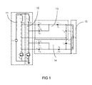
- FIG. 1 is a circuit schematic diagram showing the operating mode 1 of the invention.
- FIG. 2 is a circuit schematic diagram showing the operating mode 2 of the invention.
- FIG. 3 is a circuit schematic diagram showing the operating mode 3 of the invention.
- FIG. 4 is a circuit schematic diagram showing the operating mode 4 of the invention.
- FIG. 5 is a circuit schematic diagram showing another embodiment of the invention.
- the invention providing a “high boost ratio DC converter”, mainly including: a first switch circuit 11 , a second switch circuit 12 , a first storage circuit 13 , a second storage circuit 14 and a load circuit 15 .
- the first switch circuit 11 connects to a DC power supply Vin, which has at least one first inductor L 1 and at least one first switch S 1 .
- the second switch circuit 12 connects to the first switch circuit 11 , which has at least one second inductor L 2 and at least one second switch S 2 .
- the first storage circuit 13 connects to the second switch circuit 12 , which has at least one set of diodes, Db 1 and D 1 , at least one first clamp capacitor Cb 1 and at least one first output capacitor Co 1 .
- the second storage circuit 14 connects to the second switch circuit 12 , which has at least one second set of diodes Db 2 , and D 2 , at least one second clamp capacitor Cb 2 , and at least one second output capacitor Co 2 .
- the load circuit 15 connects to the first output capacitor Col and the second output capacitor Co 2 , which set at least one load R, so that the first output capacitor Col, and the second output capacitor Co 2 can discharge the load R.
- the first and second switches are controlled by a control chip (not shown in the figures) and the control chip controls the first and second switches in the following sequences: operating mode 1 : the first and second switches both conduct (as shown in FIG. 1 ); operating mode 2 : the first switch conducts and the second switch is cut off (as shown in FIG. 2 ); operating mode 3 : the first and second switches both conduct (as shown in FIG. 3 ); operating mode 4 : the first switch is cut off and the second switch conducts (as shown in FIG.
- the boost ratio of the DC converter is 4/(1 ⁇ D) (wherein D is the conductive cycle of the first switch and the second switch controlled by the controlling chip, simply referred to as the duty cycle), which is not only a high conversion ratio without any transformer but also decreases losses when switching the switch and when conducting as to aid and increase the efficiency of the high boost ratio DC converter.
- the load R can be for an electrical device (such as: household electrical appliances, computers, mobile phones, lighting devices. . . etc.).
- the DC power supply Vin can be a solar cell or a fuel cell.
- both the first switch S 1 and the second switch S 2 conduct, the voltage across the first inductor L 1 and the second inductor L 2 makes the current of the first inductor L 1 and the second inductor L 2 increase linearly so as to store the energy.
- the current of load-R is provided by the first output capacitor Co 1 and the second output capacitor Co 2 .
- the first switch S 1 when in operating mode 2 , the first switch S 1 conducts continuously, and the current of the inductor increases linearly to store the energy.
- the second switch S 2 is cut off, the second inductor L 2 will respectively charge the second clamp capacitor Cb 2 and discharge to the first output capacitor Co 1 with the first clamp capacitor Cb 1 .
- the potential of the first output capacitor Co 1 is shown as below, which utilizes the concept of charge and discharge, and this operation mode also meets the voltage law.
- both the first switch S 1 and the second switch S 2 conduct, the voltage across the first inductor L 1 and the second inductor L 2 makes the current of the first inductor L 1 and the second inductor L 2 increase linearly so as to store the energy.
- the current of load-R is provided by the first output capacitor Co 1 and the second output capacitor Co 2 .
- the second switch S 2 when in operating mode 4 , the second switch S 2 conducts continuously, and the current of the inductor increases linearly to store the energy.
- the first switch S 1 is cut off, the first inductor L 1 will respectively charge the first clamp capacitor Cb 1 and discharge to the second output capacitor Co 2 with the second clamp capacitor Cb 2 .
- the potential of the second output capacitor Co 2 is shown as below, which utilizes another auxiliary boost circuit set, but in the opposite direction. This kind of circuit connection can make the second output capacitor Co 2 charge normally and conform to voltage law.
- X 1 V i ⁇ ⁇ n ( 1 - D )
- X 2 - V i ⁇ ⁇ n ( 1 - D )
- X 3 V i ⁇ ⁇ n ( 1 - D )
- V Co ⁇ ⁇ 2 2 ⁇ V i ⁇ ⁇ n ( 1 - D )
- the high boost ratio DC converter of the present invention which has applications not only in renewable energy as shown in FIG. 5 , but also used in high-voltage pressure equipment for medical use. According to U.S. Safety requirements, when exceeding a certain wattage, an isolation transformer must be added, therefore an isolation transformer 16 is added in front of the present invention.
- the isolation transformer 16 is added, which can achieve electrical isolation between the load R and DC power supply Vin. And the overall gain of the circuit can be significantly improved and become 4N/(1 ⁇ D) after transformer 16 is added (wherein D is the conductive cycle of the first switch and the second switch controlled by the controlling chip, simply referred to as the duty cycle, and N refers to the number of turns on the coil of the transformer).
- the high boost ratio DC converter of the present invention can improve the circuit gain to 4/(1 ⁇ D) by using a high boost, low voltage cross switch and automatic current sharing structure when transformer 16 is not added (wherein D is the conductive cycle of the first switch and the second switch controlled by the controlling chip, simply referred to as the duty cycle).
- a transformer 16 is put in front of the invention circuit as the isolation transformer, which not only maintains the advantage of automatic current sharing and a low voltage cross switch, but also further increases the overall circuit gain as 4N/(1 ⁇ D) (wherein D is the conductive cycle of the first switch and the second switch controlled by the controlling chip, simply referred to as the duty cycle, and N refers to the number of coil turns of the transformer).
Abstract
Description
- 1. Field of the invention The present invention relates to a direct current (DC) converter with a high boost ratio, in particular, to a high boost ratio DC converter based on the integration of a multiple voltage converter and an auxiliary boost circuit, whereby changing the circuit topology not only has the advantage of initiating current flow, but also results in the circuit components not requiring a high voltage load carrying capability so as to decrease losses when switching the switch and when conducting so as to aid and increase the efficiency of the high boost ratio DC converter.
- 2. Description of Related Art
- The use of energy leads to the development of human civilization, and large enterprises around the world have gradually noted the seriousness of oil pollution, and gradually alternative energies such as solar and fuel cells have begun to be developed. For example, solar power generation utilizes photoelectric conversion to convert the photoelectrons into a DC voltage, however this needs a high boost ratio converter to boost the voltage to a sufficiently high DC link voltage if supplying electric power to a general household, so as to enable the DC-AC converter to output alternating current (AC) voltage to power general household appliances.
- According to a traditional DC boost converter which discloses a zigzag device having N-legged cores, wherein N is the number of phases which is greater than or equal to 2; a plurality of diodes, each P side of the diodes connected to each leg of the cores of the device; and a plurality of transistors, and each drain terminal of the transistors connected to each leg of the cores of the device.
- However, the transformer of the conventional DC boost converter is non-isolated, which has cores able to work in a high-frequency environment. Although a conventional DC boost converter with a high frequency zigzag transformer is capable of reducing current ripple, simplifying current control, and achieving better transient response, the converter still has the following disadvantages: increasing the converter size and cost, the Core loss and Copper loss of the transformer reducing the overall efficiency of the converter, and the energy leakage increases the stresses on the switch.
- Thus, there are still a lot of drawbacks in the above mentioned conventional goods, which are not of a good design and need to be amended.
- In view of the shortcomings derived from a conventional DC boost converter, the inventor is eager to modify and innovate, and after years of painstaking research requiring great concentration, has finally successfully developed the high boost ratio DC converter of the invention.
- The purpose of the present invention is to provide a high boost ratio DC converter, which has a high conversion ratio without any transformers.
- Another purpose of the present invention is to provide a high boost ratio DC converter, which not only has the advantage of initiating current flow, but also has circuit components not requiring a high voltage load carrying capability, thus decreasing losses when switching the switch and when conducting as to aid and increase the efficiency of the high boost ratio DC converter.
- The foregoing purpose of the invention can be achieved by a high boost ratio DC converter, including: a first switch circuit, a second switch circuit, a second storage circuit and a load circuit;
- Wherein, the first switch circuit is connected to a DC power supply, the first switch circuit having at least one first inductor and at least one first switch; the second switch circuit connects to the first switch circuit, the second switch circuit having at least one second inductor and at least one second switch;
- The first storage circuit connecting to the second switch circuit, the first storage circuit having at least one set of diodes, at least one first clamp capacitor and at least one first output capacitor; the second storage circuit connecting to the second circuit, the second storage circuit having at least one set of diodes, at least one second clamp capacitor and at least one second output capacitor;
- the load carrying circuit connecting to the first output capacitor and the second output capacitor, the load carrying circuit having at least one load, making the first and second output capacitors discharge the load;
- When using, the first and second switches are controlled by a control chip and the control chip controls the first and second switches in the following sequences: operating mode 1: the first and second switches both conduct; operating mode 2: the first switch conducts and the second switch is cut off; operating mode 3: the first and second switches both conduct; operating mode 4: the first switch is cut off and the second switch conducts thus making the first and second inductors charge to the first and second clamp capacitors, and making the first and second clamp capacitors discharge to the first and second output capacitors, and making the first and second output capacitors discharge the load, the load voltage output from the DC power supply will be boosted owing to the discharging of the first and second output capacitors. The boost ratio of the DC converter is 4/(1−D), which is not only a high conversion ratio without any transformer but also decreases losses when switching the switch and when conducting as to aid and increase the efficiency of the high boost ratio DC converter.
- The invention, as well as its many advantages, may be further understood by the following detailed description and drawings in which:
-
FIG. 1 is a circuit schematic diagram showing theoperating mode 1 of the invention. -
FIG. 2 is a circuit schematic diagram showing theoperating mode 2 of the invention. -
FIG. 3 is a circuit schematic diagram showing the operating mode 3 of the invention. -
FIG. 4 is a circuit schematic diagram showing the operating mode 4 of the invention. -
FIG. 5 is a circuit schematic diagram showing another embodiment of the invention. - Please refer to
FIG. 1 , the invention providing a “high boost ratio DC converter”, mainly including: afirst switch circuit 11, asecond switch circuit 12, afirst storage circuit 13, asecond storage circuit 14 and aload circuit 15. - Wherein, the
first switch circuit 11 connects to a DC power supply Vin, which has at least one first inductor L1 and at least one first switch S1. - The
second switch circuit 12 connects to thefirst switch circuit 11, which has at least one second inductor L2 and at least one second switch S2. - The
first storage circuit 13 connects to thesecond switch circuit 12, which has at least one set of diodes, Db1 and D1, at least one first clamp capacitor Cb1 and at least one first output capacitor Co1. - The
second storage circuit 14 connects to thesecond switch circuit 12, which has at least one second set of diodes Db2, and D2, at least one second clamp capacitor Cb2, and at least one second output capacitor Co2. - The
load circuit 15 connects to the first output capacitor Col and the second output capacitor Co2, which set at least one load R, so that the first output capacitor Col, and the second output capacitor Co2 can discharge the load R. - When in use, please refer to
FIG. 2 ,FIG. 3 andFIG. 4 , the first and second switches are controlled by a control chip (not shown in the figures) and the control chip controls the first and second switches in the following sequences: operating mode 1: the first and second switches both conduct (as shown inFIG. 1 ); operating mode 2: the first switch conducts and the second switch is cut off (as shown inFIG. 2 ); operating mode 3: the first and second switches both conduct (as shown inFIG. 3 ); operating mode 4: the first switch is cut off and the second switch conducts (as shown inFIG. 4 ) thus making the first and second inductors charge to the first and second clamp capacitors, and making the first and second clamp capacitors discharge to the first and second output capacitors, and making the first and second output capacitors discharge the load, the load voltage output from the DC power supply will be boosted owing to the discharging of the load by the first and second output capacitors. The boost ratio of the DC converter is 4/(1−D) (wherein D is the conductive cycle of the first switch and the second switch controlled by the controlling chip, simply referred to as the duty cycle), which is not only a high conversion ratio without any transformer but also decreases losses when switching the switch and when conducting as to aid and increase the efficiency of the high boost ratio DC converter. - Also, the load R can be for an electrical device (such as: household electrical appliances, computers, mobile phones, lighting devices. . . etc.). The DC power supply Vin can be a solar cell or a fuel cell.
- Please refer to
FIG. 1 , when inoperating mode 1, both the first switch S1 and the second switch S2 conduct, the voltage across the first inductor L1 and the second inductor L2 makes the current of the first inductor L1 and the second inductor L2 increase linearly so as to store the energy. The current of load-R is provided by the first output capacitor Co1 and the second output capacitor Co2. - Please refer to
FIG. 2 , when inoperating mode 2, the first switch S1 conducts continuously, and the current of the inductor increases linearly to store the energy. The second switch S2 is cut off, the second inductor L2 will respectively charge the second clamp capacitor Cb2 and discharge to the first output capacitor Co1 with the first clamp capacitor Cb1. - In this mode, the potential of the first output capacitor Co1 is shown as below, which utilizes the concept of charge and discharge, and this operation mode also meets the voltage law.
-
- Please refer to
FIG. 3 , when in operating mode 3, both the first switch S1 and the second switch S2 conduct, the voltage across the first inductor L1 and the second inductor L2 makes the current of the first inductor L1 and the second inductor L2 increase linearly so as to store the energy. The current of load-R is provided by the first output capacitor Co1 and the second output capacitor Co2. - Please refer to
FIG. 4 , when in operating mode 4, the second switch S2 conducts continuously, and the current of the inductor increases linearly to store the energy. The first switch S1 is cut off, the first inductor L1 will respectively charge the first clamp capacitor Cb1 and discharge to the second output capacitor Co2 with the second clamp capacitor Cb2. - In this mode, the potential of the second output capacitor Co2 is shown as below, which utilizes another auxiliary boost circuit set, but in the opposite direction. This kind of circuit connection can make the second output capacitor Co2 charge normally and conform to voltage law.
-
- In another embodiment of the invention, the high boost ratio DC converter of the present invention, which has applications not only in renewable energy as shown in
FIG. 5 , but also used in high-voltage pressure equipment for medical use. According to U.S. Safety requirements, when exceeding a certain wattage, an isolation transformer must be added, therefore anisolation transformer 16 is added in front of the present invention. - As shown in
FIG. 5 , theisolation transformer 16 is added, which can achieve electrical isolation between the load R and DC power supply Vin. And the overall gain of the circuit can be significantly improved and become 4N/(1−D) aftertransformer 16 is added (wherein D is the conductive cycle of the first switch and the second switch controlled by the controlling chip, simply referred to as the duty cycle, and N refers to the number of turns on the coil of the transformer). - Therefore, the high boost ratio DC converter of the present invention can improve the circuit gain to 4/(1−D) by using a high boost, low voltage cross switch and automatic current sharing structure when
transformer 16 is not added (wherein D is the conductive cycle of the first switch and the second switch controlled by the controlling chip, simply referred to as the duty cycle). - Meanwhile, in order to apply the high voltage and electrical isolation, a
transformer 16 is put in front of the invention circuit as the isolation transformer, which not only maintains the advantage of automatic current sharing and a low voltage cross switch, but also further increases the overall circuit gain as 4N/(1−D) (wherein D is the conductive cycle of the first switch and the second switch controlled by the controlling chip, simply referred to as the duty cycle, and N refers to the number of coil turns of the transformer). - Comparing the high boost ratio DC converter of the present invention with the foregoing cited case and other conventional technologies, the present invention has the following additional advantages:
-
- 1. a high conversion ratio;
- 2. it not only has a high conversion ratio without any transformer, but also decreases losses when switching the switch and when conducting as to aid and increase the efficiency of the high boost ratio DC converter.
- Many changes and modifications in the above described embodiment of the invention can, of course, be carried out without departing from the scope thereof Accordingly, to promote the progress in science and the useful arts, the invention is disclosed and is intended to be limited only by the scope of the appended claims.
Claims (6)
Applications Claiming Priority (3)
| Application Number | Priority Date | Filing Date | Title |
|---|---|---|---|
| TW100111203A | 2011-03-31 | ||
| TW100111203A TWI429176B (en) | 2011-03-31 | 2011-03-31 | High boost ratio dc converter |
| TW100111203 | 2011-03-31 |
Publications (2)
| Publication Number | Publication Date |
|---|---|
| US20120249100A1 true US20120249100A1 (en) | 2012-10-04 |
| US8503198B2 US8503198B2 (en) | 2013-08-06 |
Family
ID=46926341
Family Applications (1)
| Application Number | Title | Priority Date | Filing Date |
|---|---|---|---|
| US13/107,844 Expired - Fee Related US8503198B2 (en) | 2011-03-31 | 2011-05-13 | High boost ratio DC converter |
Country Status (2)
| Country | Link |
|---|---|
| US (1) | US8503198B2 (en) |
| TW (1) | TWI429176B (en) |
Cited By (6)
| Publication number | Priority date | Publication date | Assignee | Title |
|---|---|---|---|---|
| CN104104232A (en) * | 2014-07-02 | 2014-10-15 | 三峡大学 | Isolated high-gain DC/DC (Direct Current) converter |
| US20150131330A1 (en) * | 2013-11-14 | 2015-05-14 | National Tsing Hua University | Bidirectional dc-dc converter system and circuit thereof |
| CN108599591A (en) * | 2018-06-06 | 2018-09-28 | 三峡大学 | One kind is from the high boost rectifier of current-sharing module large capacity |
| CN110611425A (en) * | 2019-08-30 | 2019-12-24 | 电子科技大学 | Current sharing method based on series-parallel Boost converter |
| US10530162B2 (en) | 2014-06-20 | 2020-01-07 | Katholieke Universiteit Leuven | Methods and devices for increasing the voltage gain range of a DC-DC power converter |
| US11128222B2 (en) * | 2017-08-23 | 2021-09-21 | Mitsubishi Electric Corporation | DC/DC converter |
Families Citing this family (2)
| Publication number | Priority date | Publication date | Assignee | Title |
|---|---|---|---|---|
| TWI495242B (en) * | 2013-10-09 | 2015-08-01 | Nat Univ Tsing Hua | Bidirectional dc-dc converter |
| US9582016B2 (en) * | 2015-02-05 | 2017-02-28 | Silicon Laboratories Inc. | Boost converter with capacitive boost stages |
Citations (13)
| Publication number | Priority date | Publication date | Assignee | Title |
|---|---|---|---|---|
| US5598326A (en) * | 1994-02-10 | 1997-01-28 | Philips Electronics North America | High frequency AC/AC converter with PF correction |
| US5627737A (en) * | 1993-09-13 | 1997-05-06 | Sanyo Electric Co., Ltd. | Power inverter for use in system interconnection |
| US6239584B1 (en) * | 2000-06-20 | 2001-05-29 | Delta Electronics, Inc. | Two-inductor boost converter |
| US20030103362A1 (en) * | 2001-12-03 | 2003-06-05 | Hongjian Gan | Constant voltage reset circuit for forward converter |
| US20040027842A1 (en) * | 2002-06-05 | 2004-02-12 | Omron Corporation | Electric power conversion device with push-pull circuitry |
| US20040184289A1 (en) * | 2002-01-31 | 2004-09-23 | Vlt Corporation, A Texas Corporation | Output resistance modulation in power converters |
| US6989997B2 (en) * | 2003-06-25 | 2006-01-24 | Virginia Tech Intellectual Properties, Inc. | Quasi-resonant DC-DC converters with reduced body diode loss |
| US20060171181A1 (en) * | 2003-03-17 | 2006-08-03 | Robert Clavel | Sinewave inverter using hybrid regulator |
| US7480156B1 (en) * | 2006-01-07 | 2009-01-20 | Wittenbreder Jr Ernest Henry | Tapped inductor power conversion networks |
| US20090244944A1 (en) * | 2008-03-25 | 2009-10-01 | Delta Electronics, Inc. | Power converter system that operates efficiently over a range of load conditions |
| US20100085032A1 (en) * | 2008-10-07 | 2010-04-08 | Hungkuang University | Boost Device for Voltage Boosting |
| US20110205762A1 (en) * | 2010-02-24 | 2011-08-25 | Ching-Tsai Pan | Integrated-type high step-up ratio dc-ac conversion circuit with auxiliary step-up circuit |
| US20120025720A1 (en) * | 2010-07-27 | 2012-02-02 | Bcd Semiconductor Manufacturing Limited | Power supply apparatus and method for a backlight system |
-
2011
- 2011-03-31 TW TW100111203A patent/TWI429176B/en not_active IP Right Cessation
- 2011-05-13 US US13/107,844 patent/US8503198B2/en not_active Expired - Fee Related
Patent Citations (13)
| Publication number | Priority date | Publication date | Assignee | Title |
|---|---|---|---|---|
| US5627737A (en) * | 1993-09-13 | 1997-05-06 | Sanyo Electric Co., Ltd. | Power inverter for use in system interconnection |
| US5598326A (en) * | 1994-02-10 | 1997-01-28 | Philips Electronics North America | High frequency AC/AC converter with PF correction |
| US6239584B1 (en) * | 2000-06-20 | 2001-05-29 | Delta Electronics, Inc. | Two-inductor boost converter |
| US20030103362A1 (en) * | 2001-12-03 | 2003-06-05 | Hongjian Gan | Constant voltage reset circuit for forward converter |
| US20040184289A1 (en) * | 2002-01-31 | 2004-09-23 | Vlt Corporation, A Texas Corporation | Output resistance modulation in power converters |
| US20040027842A1 (en) * | 2002-06-05 | 2004-02-12 | Omron Corporation | Electric power conversion device with push-pull circuitry |
| US20060171181A1 (en) * | 2003-03-17 | 2006-08-03 | Robert Clavel | Sinewave inverter using hybrid regulator |
| US6989997B2 (en) * | 2003-06-25 | 2006-01-24 | Virginia Tech Intellectual Properties, Inc. | Quasi-resonant DC-DC converters with reduced body diode loss |
| US7480156B1 (en) * | 2006-01-07 | 2009-01-20 | Wittenbreder Jr Ernest Henry | Tapped inductor power conversion networks |
| US20090244944A1 (en) * | 2008-03-25 | 2009-10-01 | Delta Electronics, Inc. | Power converter system that operates efficiently over a range of load conditions |
| US20100085032A1 (en) * | 2008-10-07 | 2010-04-08 | Hungkuang University | Boost Device for Voltage Boosting |
| US20110205762A1 (en) * | 2010-02-24 | 2011-08-25 | Ching-Tsai Pan | Integrated-type high step-up ratio dc-ac conversion circuit with auxiliary step-up circuit |
| US20120025720A1 (en) * | 2010-07-27 | 2012-02-02 | Bcd Semiconductor Manufacturing Limited | Power supply apparatus and method for a backlight system |
Cited By (6)
| Publication number | Priority date | Publication date | Assignee | Title |
|---|---|---|---|---|
| US20150131330A1 (en) * | 2013-11-14 | 2015-05-14 | National Tsing Hua University | Bidirectional dc-dc converter system and circuit thereof |
| US10530162B2 (en) | 2014-06-20 | 2020-01-07 | Katholieke Universiteit Leuven | Methods and devices for increasing the voltage gain range of a DC-DC power converter |
| CN104104232A (en) * | 2014-07-02 | 2014-10-15 | 三峡大学 | Isolated high-gain DC/DC (Direct Current) converter |
| US11128222B2 (en) * | 2017-08-23 | 2021-09-21 | Mitsubishi Electric Corporation | DC/DC converter |
| CN108599591A (en) * | 2018-06-06 | 2018-09-28 | 三峡大学 | One kind is from the high boost rectifier of current-sharing module large capacity |
| CN110611425A (en) * | 2019-08-30 | 2019-12-24 | 电子科技大学 | Current sharing method based on series-parallel Boost converter |
Also Published As
| Publication number | Publication date |
|---|---|
| TWI429176B (en) | 2014-03-01 |
| US8503198B2 (en) | 2013-08-06 |
| TW201240302A (en) | 2012-10-01 |
Similar Documents
| Publication | Publication Date | Title |
|---|---|---|
| US8503198B2 (en) | High boost ratio DC converter | |
| Maheri et al. | High step-up DC–DC converter with minimum output voltage ripple | |
| Prabhala et al. | A DC–DC converter with high voltage gain and two input boost stages | |
| Hsieh et al. | High-conversion-ratio bidirectional DC–DC converter with coupled inductor | |
| Tseng et al. | High step-up high-efficiency interleaved converter with voltage multiplier module for renewable energy system | |
| Mohseni et al. | A new soft switching DC–DC converter with high voltage gain capability | |
| Tseng et al. | A single-switch converter with high step-up gain and low diode voltage stress suitable for green power-source conversion | |
| Schmitz et al. | High step-up nonisolated ZVS/ZCS DC–DC converter for photovoltaic thin-film module applications | |
| Liu et al. | Interleaved high step-up converter with coupled inductor and voltage multiplier for renewable energy system | |
| Tang et al. | Study of an improved dual-switch converter with passive lossless clamping | |
| CN102638164B (en) | High boost circuit, solar inverter and solar cell system | |
| Mira et al. | Review of high efficiency bidirectional dc-dc topologies with high voltage gain | |
| CN105978322B (en) | A kind of quasi- sources Z DC-DC converter of switching capacity type high-gain | |
| Barbi | A high step-up gain DC-DC converter based on the stacking of three conventional buck boost DC-DC converters | |
| Ghasemi et al. | A new isolated SEPIC converter with coupled inductors for photovoltaic applications | |
| Priya et al. | Comparison of n-stage cascade cockcroft-walton voltage multiplier applied to transformer-less dc-dc boost converter | |
| Tanca et al. | Nonisolated high step-up stacked dc-dc converter based on boost converter elements for high power application | |
| Mbobda et al. | A dual-switch cubic SEPIC converter with extra high voltage gain | |
| Sadaf et al. | A new type of boost converter with dual duty and high gain for dc microgrid applications | |
| Silveira et al. | Analysis and small-signal modeling of a nonisolated high voltage step-up dc-dc boost converter | |
| Salvador et al. | Nonisolated high step‐up DC‐DC interleaved SEPIC converter based on voltage multiplier cells | |
| Chen et al. | A isolated bidirectional interleaved flyback converter for battery backup system application | |
| Zamani et al. | Design and implementation of nonisolated high step-up DC-DC converter | |
| KR101155986B1 (en) | Multi-phase dc-dc converter using integrated y-y connection transformer for fuel-cell system | |
| TW201608810A (en) | Interlaced direct current converter |
Legal Events
| Date | Code | Title | Description |
|---|---|---|---|
| AS | Assignment |
Owner name: NATIONAL TSING HUA UNIVERSITY, TAIWAN Free format text: ASSIGNMENT OF ASSIGNORS INTEREST;ASSIGNORS:PAN, CHING-TSAI;LEE, CHAO-HAN;REEL/FRAME:026280/0187 Effective date: 20110418 |
|
| STCF | Information on status: patent grant |
Free format text: PATENTED CASE |
|
| FPAY | Fee payment |
Year of fee payment: 4 |
|
| FEPP | Fee payment procedure |
Free format text: MAINTENANCE FEE REMINDER MAILED (ORIGINAL EVENT CODE: REM.); ENTITY STATUS OF PATENT OWNER: SMALL ENTITY |
|
| LAPS | Lapse for failure to pay maintenance fees |
Free format text: PATENT EXPIRED FOR FAILURE TO PAY MAINTENANCE FEES (ORIGINAL EVENT CODE: EXP.); ENTITY STATUS OF PATENT OWNER: SMALL ENTITY |
|
| STCH | Information on status: patent discontinuation |
Free format text: PATENT EXPIRED DUE TO NONPAYMENT OF MAINTENANCE FEES UNDER 37 CFR 1.362 |
|
| FP | Lapsed due to failure to pay maintenance fee |
Effective date: 20210806 |