US20120249352A1 - Switched-capacitor input circuit and analog-to-digital converter including the same - Google Patents
Switched-capacitor input circuit and analog-to-digital converter including the same Download PDFInfo
- Publication number
- US20120249352A1 US20120249352A1 US13/526,405 US201213526405A US2012249352A1 US 20120249352 A1 US20120249352 A1 US 20120249352A1 US 201213526405 A US201213526405 A US 201213526405A US 2012249352 A1 US2012249352 A1 US 2012249352A1
- Authority
- US
- United States
- Prior art keywords
- capacitor
- terminal
- reference voltage
- capacitors
- differential amplifier
- Prior art date
- Legal status (The legal status is an assumption and is not a legal conclusion. Google has not performed a legal analysis and makes no representation as to the accuracy of the status listed.)
- Granted
Links
Images


Classifications
-
- H—ELECTRICITY
- H03—ELECTRONIC CIRCUITRY
- H03M—CODING; DECODING; CODE CONVERSION IN GENERAL
- H03M1/00—Analogue/digital conversion; Digital/analogue conversion
- H03M1/06—Continuously compensating for, or preventing, undesired influence of physical parameters
- H03M1/0602—Continuously compensating for, or preventing, undesired influence of physical parameters of deviations from the desired transfer characteristic
- H03M1/0604—Continuously compensating for, or preventing, undesired influence of physical parameters of deviations from the desired transfer characteristic at one point, i.e. by adjusting a single reference value, e.g. bias or gain error
- H03M1/0607—Offset or drift compensation
-
- H—ELECTRICITY
- H03—ELECTRONIC CIRCUITRY
- H03M—CODING; DECODING; CODE CONVERSION IN GENERAL
- H03M1/00—Analogue/digital conversion; Digital/analogue conversion
- H03M1/12—Analogue/digital converters
Definitions
- the present invention relates to a switched-capacitor input circuit and an analog-to-digital converter (ADC) including the same and, for example, a method and circuit for correcting an offset component of an input signal of an ADC and, more particularly, to offset correction of an input signal of a switched-capacitor ADC.
- ADC analog-to-digital converter
- capacitors having smaller capacitance values need to be added.
- a capacitor having a capacitance value 1 ⁇ 2 needs to be added.
- a capacitor having a capacitance value 1 ⁇ 2 and a capacitor having a capacitance value 1 ⁇ 4 need to be added.
- the capacitance value is decreased to obtain a higher accuracy, the parasitic capacitances of connected wiring lines, switches, and the like become normegligible, leading to difficulty in accurately binary weighting the capacitance ratio. This makes it harder to maintain the offset correction accuracy.
- the present invention provides an input circuit capable of advantageously controlling a potential change smaller than before without using any capacitor with a small capacitance value and an analog-to-digital converter including the same.
- the first aspect of the present invention provides a switched-capacitor input circuit which receives an analog input signal, and samples and holds the analog input signal, comprising a differential amplifier, a first capacitor, one terminal of the first capacitor being connected to a non-inverting input terminal of the differential amplifier, a second capacitor, one terminal of the second capacitor being connected to an inverting input terminal of the differential amplifier, a first switch configured to connect the other terminal of the first capacitor to one of a first reference voltage and a second reference voltage, a second switch configured to connect the other terminal of the second capacitor to one of the first reference voltage and the second reference voltage, and a third switch configured to connect the other terminal of the first capacitor to the other terminal of the second capacitor, wherein upon sampling, the first switch connects the other terminal of the first capacitor to the first reference voltage, and the second switch connects the other terminal of the second capacitor to the second reference voltage, and upon holding, the third switch connects the other terminal of the first capacitor to the other terminal of the second capacitor.
- the second aspect of the present invention provides a switched-capacitor input circuit which receives an analog input signal, and samples and holds the analog input signal, comprising a differential amplifier, a first capacitor, one terminal of the first capacitor being connected to a non-inverting input terminal of the differential amplifier, a second capacitor, one terminal of the second capacitor being connected to an inverting input terminal of the differential amplifier, a first switch configured to connect the other terminal of the first capacitor to one of a first reference voltage and a second reference voltage, a second switch configured to connect the other terminal of the second capacitor to one of the first reference voltage and the second reference voltage, and a third switch configured to connect the other terminal of the first capacitor to the other terminal of the second capacitor, wherein upon sampling, the third switch connects the other terminal of the first capacitor to the other terminal of the second capacitor, and upon holding, the first switch connects the other terminal of the first capacitor to the first reference voltage, and the second switch connects the other terminal of the second capacitor to the second reference voltage.
- the third aspect of the present invention provides an analog-to-digital converter comprising the input circuit as defined above, and an analog-to-digital conversion circuit configured to perform analog-to-digital conversion of an output signal from the input circuit.
- the input terminals of first and second offset correction capacitors are short-circuited so as to obtain a function of causing charge movement between the two capacitors and thus decreasing the potential change on the output terminal side of a differential amplifier.
- This allows control of a potential change smaller than before without using any capacitor with a small capacitance value. It is therefore possible to implement a more accurate, binary weighted offset correction amount and accurately perform offset correction in an analog-to-digital converter.
- FIG. 1A is a block diagram showing an example of the arrangement of an analog-to-digital converter according to the first embodiment
- FIG. 1B is a view showing an example of a switch control table according to the first embodiment
- FIG. 2A is a connection diagram showing the state of a sample and hold circuit according to the first embodiment upon sampling
- FIG. 2B is a connection diagram showing the state of the sample and hold circuit according to the first embodiment upon holding without offset correction
- FIGS. 3A and 3B are connection diagrams showing the states of the sample and hold circuit according to the first embodiment upon holding with offset correction;
- FIG. 4 is a flowchart illustrating an example of the processing procedure of a switch controller according to the embodiment
- FIG. 5A is a block diagram showing an example of the arrangement of an analog-to-digital converter according to the second embodiment
- FIG. 5B is a view showing an example of a switch control table according to the second embodiment
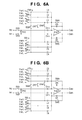
- FIG. 6A is a connection diagram showing the state of a sample and hold circuit according to the second embodiment upon sampling
- FIG. 6B is a connection diagram showing the state of the sample and hold circuit according to the second embodiment upon holding without offset correction.
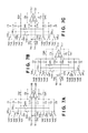
- FIGS. 7A to 7C are connection diagrams showing the states of the sample and hold circuit according to the second embodiment upon holding with offset correction.
- FIGS. 1A to 4 An arrangement and operation according to the first embodiment of the present invention will be described with reference to FIGS. 1A to 4 .
- a sample and hold circuit 101 serving as an input circuit receives differential analog input signals input to input terminals Inp and Inn, samples and holds the signals, and outputs them to output terminals Outp and Outn.
- An analog-to-digital conversion circuit 102 receives the output signals, converts them into digital data, and outputs it to an output terminal Dout.
- VrefL and VrefH are lower and higher reference voltages, respectively.
- the analog-to-digital conversion circuit 102 compares the two reference voltages with the voltages of the analog input signals, and converts the analog input signals into digital data. In the first embodiment, the two reference voltages are supplied to the sample and hold circuit 101 as well and used for input offset correction.
- a switch controller 103 outputs control signals to control switching in the sample and hold circuit 101 and the analog-to-digital conversion circuit 102 .
- the switch controller 103 has a switch control table 103 a that stores combinations of control signals to switches corresponding to the statuses of each circuit and offset correction values.
- the switch control table 103 a in FIG. 1B stores control signals to control the switches in correspondence with the statuses of the sample and hold circuit 101 and offset correction values.
- the control signals in detailed examples of the sample and hold circuit 101 shown in FIGS. 2A , 2 B, 3 A, and 3 B are represented by the states of switches.
- the offset correction in FIG. 1B is done by binary weighting of three bits, that is, lower, intermediate, and higher bits.
- FIG. 2A is a circuit diagram of the switched-capacitor sample and hold circuit 101 in FIG. 1A , which illustrates the connection state upon sampling.
- Amp 1 is a differential amplifier having a non-inverting input terminal and an inverting input terminal
- Cinp and Cinn are input capacitors
- Cfp and Cfn are feedback capacitors.
- C 1 to C 3 are first capacitors for offset correction
- C 4 to C 6 are second capacitors for offset correction.
- One terminal of each of the capacitors C 1 to C 6 is connected to the differential amplifier, and the other terminal is connected to the first or second reference voltage via a corresponding one of first switches SW C1 to SW C3 and second switches SW C4 to SW C6 .
- the capacitors C 1 to C 3 serve as a plurality of first capacitive elements of a first capacitor for offset correction
- the capacitors C 4 to C 6 serve as a plurality of second capacitive elements of a second capacitor for offset correction.
- the capacitors C 1 , C 2 , C 4 , and C 5 have the same capacitance value that is not binary weighted. However, since the connection destinations are different, binary weighting is implemented by an offset correction value that appears as an output voltage. Referring to FIG.
- the terminals of the capacitors Cfp and Cfn are short-circuited by switches SW 4 and SW 5 so as to reset the outputs Outp and Outn.
- the capacitors Cinp and Cinn are connected to the inputs Inp and Inn via switches SW 1 and SW 2 so as to store the input signals in the capacitors Cinp and Cinn.
- the capacitors C 1 to C 3 are connected to the reference voltage VrefH, and the capacitors C 4 to C 6 are connected to the reference voltage VrefL to accumulate charges.
- FIG. 2B is a circuit diagram showing the connection state of the sample and hold circuit 101 upon holding without offset component correction. This indicates the state upon holding with offset correction (000) in FIG. 1B .
- FIG. 3A is a circuit diagram showing the connection state of the sample and hold circuit 101 upon holding with correction of a first offset amount. Even in this case, the sampling state is the same as in FIG. 2A .
- the connection states of the capacitors C 1 and C 4 are different from those in the holding state without offset correction shown in FIG. 2B .
- the capacitor C 1 is connected to the reference voltage VrefH
- the capacitor C 4 is connected to the reference voltage VrefL.
- a third switch SW 6 short-circuits the capacitors C 1 and C 4 to set them at an equipotential. Charges accumulated in the capacitors C 1 and C 4 then move to the capacitors Cfp and Cfn, and affect the output voltage.
- FIG. 3B is a circuit diagram showing the connection state of the sample and hold circuit 101 upon holding with correction of a second offset amount. Even in this case, the sampling state is the same as in FIG. 2A .
- the connection states of the capacitors C 2 and C 5 are different from those in the holding state without offset correction shown in FIG. 2B .
- the capacitor C 2 is connected to the reference voltage VrefH, and the capacitor C 5 is connected to the reference voltage VrefL.
- the capacitor C 2 is connected to the reference voltage VrefL, and the capacitor C 5 is connected to the reference voltage VrefH.
- the switch controller 103 determines in step S 41 based on digital data output from the analog-to-digital conversion circuit 102 whether offset change is necessary. If necessary, in step S 42 , the switch controller 103 selects a combination of switch settings corresponding to the offset correction value from the table shown in FIG. 1B . In step S 43 , the switch controller 103 holds the selected switch setting combination for offset correction from then on. In step S 44 , the switch controller 103 outputs, to the sample and hold circuit 101 , switch control signals based on the new switch setting combination set in step S 43 or a previous switch setting combination (if NO in step S 41 ). This control procedure may be either executed as software under the CPU of the switch controller 103 or incorporated in the switch controller 103 as hardware.
- the capacitors C 1 , C 2 , C 4 , and C 5 have the same capacitance value.
- the offset correction amount can be 1 ⁇ 2.
- the analog-to-digital conversion circuit 102 requires two kinds of reference voltages, that is, lower and higher reference voltages. However, sharing VrefL and VrefH as these reference voltages obviates the necessity of preparing a new reference voltage.
- the differential positive- and negative-side offset correction capacitors are short-circuited. Using this method allows to change the potential change amount without newly preparing a third reference voltage.
- the method of the present invention makes it possible to perform offset correction in a small amount without providing any capacitive element having a small capacitance value.
- an offset correction amount binary weighted at 1:2:4 can be obtained. It is therefore possible to implement a 3-bit accuracy, that is, an offset correction accuracy in eight steps without making the minimum capacitance value (corresponding to the capacitors C 1 and C 4 in this circuit) smaller.
- the capacitor C 1 is connected to the reference voltage VrefH while the capacitor C 4 is connected to the reference voltage VrefL upon sampling, and the capacitors C 1 and C 4 are short-circuited upon holding, thereby implementing offset correction of 0.2 ⁇ (VrefH ⁇ VrefL).
- another connection method can also implement offset correction in the same amount. For example, even when the circuit operates so as to short-circuit the capacitors C 1 and C 4 upon sampling, and connect the capacitor C 1 to the reference voltage VrefL and the capacitor C 4 to the reference voltage VrefH upon holding, offset correction of 0.2 ⁇ (VrefH ⁇ VrefL) can be implemented.
- FIGS. 5A to 7C An arrangement and operation according to the second embodiment of the present invention will be described with reference to FIGS. 5A to 7C .
- a differential sample and hold circuit 201 samples differential analog signals input to input terminals Inp and Inn.
- the sample and hold circuit 201 holds the signals, and outputs them to output terminals Outp and Outn.
- a differential analog-to-digital conversion circuit 202 receives the output signals, converts them into digital data, and outputs it to an output terminal Dout.
- VrefL and VrefH are lower and higher reference voltages, respectively.
- the differential analog-to-digital conversion circuit 202 compares the two reference voltages with the voltages of the input analog signals, and converts the signals into digital data. In this embodiment, the two potentials are supplied to the differential sample and hold circuit 201 as well and used for input offset correction.
- a switch controller 203 outputs control signals to control switching in the sample and hold circuit 201 and the analog-to-digital conversion circuit 202 .
- the switch controller 203 has a switch control table 203 a that stores combinations of control signals to switches corresponding to the statuses of each circuit and offset correction values. Note that the outline of processing of the switch controller 203 is the same as in the flowchart of FIG. 4 according to the first embodiment.
- the switch control table 203 a in FIG. 5B stores control signals to control the switches in correspondence with the offset correction values of the sample and hold circuit 201 .
- the control signals in detailed examples of the sample and hold circuit 201 shown in FIGS. 6A , 6 B, and 7 A to 7 C are represented by the states of switches.
- the offset correction in FIG. 5B is done by ternary weighting of three bits, that is, lower, intermediate, and higher bits. Note that the states of switches SW 1 to SW 5 corresponding to the statuses of the sample and hold circuit 201 are the same as in the first embodiment in FIG. 1B , and a description thereof will not be repeated.
- FIG. 6A is a circuit diagram of the switched-capacitor sample and hold circuit 201 in FIG. 5A , which illustrates the connection state upon sampling.
- Amp 1 is a differential amplifier
- Cinp and Cinn are input capacitors
- Cfp and Cfn are feedback capacitors.
- C 1 to C 3 are first capacitors for offset correction
- C 4 to C 6 are second capacitors for offset correction.
- One terminal of each of the capacitors C 1 to C 6 is connected to the differential amplifier, and the other terminal is connected to the first or second reference voltage via a corresponding one of first switches SW C1 to SW C3 and second switches SW C4 to SW C6 .
- the capacitors C 1 to C 3 serve as a plurality of first capacitive elements of a first capacitor for offset correction
- the capacitors C 4 to C 6 serve as a plurality of second capacitive elements of a second capacitor for offset correction.
- the terminals of the capacitors Cfp and Cfn are short-circuited by switches SW 7 and SW 8 so as to reset the outputs Outp and Outn.
- the capacitors Cinp and Cinn are connected to the inputs Inp and Inn via switches SW 4 and SW 5 so as to store the input signals in the capacitors Cinp and Cinn.
- the capacitors C 1 to C 3 are connected to the reference voltage VrefH, and the capacitors C 4 to C 6 are connected to the reference voltage VrefL to accumulate charges.
- FIG. 6B is a circuit diagram showing the connection state of the sample and hold circuit 201 upon holding without offset correction.
- the switches SW 7 and SW 8 open to cancel reset.
- FIG. 7A is a circuit diagram showing the connection state of the sample and hold circuit 201 upon holding with correction of a first offset amount. Even in this case, the sampling state is the same as in FIG. 6A .
- the connection states of the capacitors C 1 and C 4 are different from those in the holding state without offset correction shown in FIG. 6B .
- the capacitor C 1 is connected to the reference voltage VrefH
- the capacitor C 4 is connected to the reference voltage VrefL.
- a switch SW 9 short-circuits the capacitors C 1 and C 4 to set them at an equipotential. Charges accumulated in the capacitors C 1 and C 4 then move to the capacitors Cfp and Cfn, and affect the output voltage.
- FIG. 7B is a circuit diagram showing the connection state of the sample and hold circuit 201 upon holding with correction of a second offset amount. Even in this case, the sampling state is the same as in FIG. 6A .
- the connection states of the capacitors C 1 and C 4 are different from those in the holding state without offset correction shown in FIG. 6B .
- the capacitor C 1 is connected to the reference voltage VrefH, and the capacitor C 4 is connected to the reference voltage VrefL.
- the capacitor C 1 is connected to the reference voltage VrefL, and the capacitor C 4 is connected to the reference voltage VrefH.
- FIG. 7C is a circuit diagram showing the connection state of the sample and hold circuit 201 upon holding with correction of a third offset amount. Even in this case, the sampling state is the same as in FIG. 6A .
- the connection states of the capacitors C 2 and C 5 are different from those in the holding state without offset correction shown in FIG. 6B .
- the capacitor C 2 is connected to the reference voltage VrefH
- the capacitor C 5 is connected to the reference voltage VrefL.
- a switch SW 10 short-circuits the capacitors C 2 and C 5 to set them at an equipotential. Charges accumulated in the capacitors C 2 and C 5 then move to the capacitors Cfp and Cfn, and affect the output voltage.
- the offset correction amount can be controlled using ternary weighted capacitors.
- ternary weighting is implemented using a method of short-circuiting the differential positive- and negative-side offset correction capacitors.
- the differential analog-to-digital conversion circuit 202 requires two kinds of reference voltages, that is, lower and higher reference voltages. However, sharing VrefL and VrefH as these reference voltages obviates the necessity of preparing a new reference voltage, and enables to further reduce the circuit scale.
- the capacitor C 1 is connected to the reference voltage VrefH while the capacitor C 4 is connected to the reference voltage VrefL upon sampling, and the capacitors C 1 and C 4 are short-circuited upon holding, thereby implementing offset correction of 0.02 ⁇ (VrefH ⁇ VrefL).
- another connection method can also implement offset correction in the same amount. For example, even when the circuit operates so as to short-circuit the capacitors C 1 and C 4 upon sampling, and connect the capacitor C 1 to the reference voltage VrefL and the capacitor C 4 to the reference voltage VrefH upon holding, offset correction of 0.02 ⁇ (VrefH ⁇ VrefL) can be implemented.
Abstract
Description
- 1. Field of the Invention
- The present invention relates to a switched-capacitor input circuit and an analog-to-digital converter (ADC) including the same and, for example, a method and circuit for correcting an offset component of an input signal of an ADC and, more particularly, to offset correction of an input signal of a switched-capacitor ADC.
- 2. Description of the Related Art
- As a circuit for removing an offset component of an input signal and extracting significant signal information in an ADC, a circuit having a capacitor for offset correction using a switched-capacitor circuit is known (Japanese Patent Laid-Open No. 2003-060505). This circuit performs offset correction at a desired accuracy using a necessary number of binary weighted capacitors.
- However, to increase the offset correction accuracy using the technique described in Japanese Patent Laid-Open No. 2003-060505, capacitors having smaller capacitance values need to be added. To double the accuracy, a capacitor having a capacitance value ½ needs to be added. To quadruple the accuracy, a capacitor having a capacitance value ½ and a capacitor having a capacitance value ¼ need to be added. When the capacitance value is decreased to obtain a higher accuracy, the parasitic capacitances of connected wiring lines, switches, and the like become normegligible, leading to difficulty in accurately binary weighting the capacitance ratio. This makes it harder to maintain the offset correction accuracy. Hence, there is actually a limit to adding capacitors with smaller capacitance values.
- The present invention provides an input circuit capable of advantageously controlling a potential change smaller than before without using any capacitor with a small capacitance value and an analog-to-digital converter including the same.
- The first aspect of the present invention provides a switched-capacitor input circuit which receives an analog input signal, and samples and holds the analog input signal, comprising a differential amplifier, a first capacitor, one terminal of the first capacitor being connected to a non-inverting input terminal of the differential amplifier, a second capacitor, one terminal of the second capacitor being connected to an inverting input terminal of the differential amplifier, a first switch configured to connect the other terminal of the first capacitor to one of a first reference voltage and a second reference voltage, a second switch configured to connect the other terminal of the second capacitor to one of the first reference voltage and the second reference voltage, and a third switch configured to connect the other terminal of the first capacitor to the other terminal of the second capacitor, wherein upon sampling, the first switch connects the other terminal of the first capacitor to the first reference voltage, and the second switch connects the other terminal of the second capacitor to the second reference voltage, and upon holding, the third switch connects the other terminal of the first capacitor to the other terminal of the second capacitor.
- The second aspect of the present invention provides a switched-capacitor input circuit which receives an analog input signal, and samples and holds the analog input signal, comprising a differential amplifier, a first capacitor, one terminal of the first capacitor being connected to a non-inverting input terminal of the differential amplifier, a second capacitor, one terminal of the second capacitor being connected to an inverting input terminal of the differential amplifier, a first switch configured to connect the other terminal of the first capacitor to one of a first reference voltage and a second reference voltage, a second switch configured to connect the other terminal of the second capacitor to one of the first reference voltage and the second reference voltage, and a third switch configured to connect the other terminal of the first capacitor to the other terminal of the second capacitor, wherein upon sampling, the third switch connects the other terminal of the first capacitor to the other terminal of the second capacitor, and upon holding, the first switch connects the other terminal of the first capacitor to the first reference voltage, and the second switch connects the other terminal of the second capacitor to the second reference voltage.
- The third aspect of the present invention provides an analog-to-digital converter comprising the input circuit as defined above, and an analog-to-digital conversion circuit configured to perform analog-to-digital conversion of an output signal from the input circuit.
- According to one aspect of the present invention, the input terminals of first and second offset correction capacitors are short-circuited so as to obtain a function of causing charge movement between the two capacitors and thus decreasing the potential change on the output terminal side of a differential amplifier. This allows control of a potential change smaller than before without using any capacitor with a small capacitance value. It is therefore possible to implement a more accurate, binary weighted offset correction amount and accurately perform offset correction in an analog-to-digital converter.
- Further features of the present invention will become apparent from the following description of exemplary embodiments with reference to the attached drawings.
-
FIG. 1A is a block diagram showing an example of the arrangement of an analog-to-digital converter according to the first embodiment; -
FIG. 1B is a view showing an example of a switch control table according to the first embodiment; -
FIG. 2A is a connection diagram showing the state of a sample and hold circuit according to the first embodiment upon sampling; -
FIG. 2B is a connection diagram showing the state of the sample and hold circuit according to the first embodiment upon holding without offset correction; -
FIGS. 3A and 3B are connection diagrams showing the states of the sample and hold circuit according to the first embodiment upon holding with offset correction; -
FIG. 4 is a flowchart illustrating an example of the processing procedure of a switch controller according to the embodiment; -
FIG. 5A is a block diagram showing an example of the arrangement of an analog-to-digital converter according to the second embodiment; -
FIG. 5B is a view showing an example of a switch control table according to the second embodiment; -
FIG. 6A is a connection diagram showing the state of a sample and hold circuit according to the second embodiment upon sampling; -
FIG. 6B is a connection diagram showing the state of the sample and hold circuit according to the second embodiment upon holding without offset correction; and -
FIGS. 7A to 7C are connection diagrams showing the states of the sample and hold circuit according to the second embodiment upon holding with offset correction. - An arrangement and operation according to the first embodiment of the present invention will be described with reference to
FIGS. 1A to 4 . - <Example of Arrangement of Analog-to-Digital Converter (ADC) of First Embodiment>
- In a differential ADC shown in
FIG. 1A , a sample andhold circuit 101 serving as an input circuit receives differential analog input signals input to input terminals Inp and Inn, samples and holds the signals, and outputs them to output terminals Outp and Outn. An analog-to-digital conversion circuit 102 receives the output signals, converts them into digital data, and outputs it to an output terminal Dout. VrefL and VrefH are lower and higher reference voltages, respectively. The analog-to-digital conversion circuit 102 compares the two reference voltages with the voltages of the analog input signals, and converts the analog input signals into digital data. In the first embodiment, the two reference voltages are supplied to the sample and holdcircuit 101 as well and used for input offset correction. Aswitch controller 103 outputs control signals to control switching in the sample and holdcircuit 101 and the analog-to-digital conversion circuit 102. Theswitch controller 103 has a switch control table 103 a that stores combinations of control signals to switches corresponding to the statuses of each circuit and offset correction values. - (Example of Arrangement of Switch Control Table 103 a)
- The switch control table 103 a in
FIG. 1B stores control signals to control the switches in correspondence with the statuses of the sample and holdcircuit 101 and offset correction values. In this example, the control signals in detailed examples of the sample and holdcircuit 101 shown inFIGS. 2A , 2B, 3A, and 3B are represented by the states of switches. The offset correction inFIG. 1B is done by binary weighting of three bits, that is, lower, intermediate, and higher bits. - <Examples of Circuit and Operation of Sample and Hold
Circuit 101> -
FIG. 2A is a circuit diagram of the switched-capacitor sample and holdcircuit 101 inFIG. 1A , which illustrates the connection state upon sampling. Amp1 is a differential amplifier having a non-inverting input terminal and an inverting input terminal, Cinp and Cinn are input capacitors, and Cfp and Cfn are feedback capacitors. C1 to C3 are first capacitors for offset correction, and C4 to C6 are second capacitors for offset correction. One terminal of each of the capacitors C1 to C6 is connected to the differential amplifier, and the other terminal is connected to the first or second reference voltage via a corresponding one of first switches SWC1 to SWC3 and second switches SWC4 to SWC6. The capacitors C1 to C3 serve as a plurality of first capacitive elements of a first capacitor for offset correction, and the capacitors C4 to C6 serve as a plurality of second capacitive elements of a second capacitor for offset correction. The capacitance ratio of the capacitors is Cinp:Cinn:Cfp:Cfn:C1:C2:C3:C4:C5:C6=10:10:5:5:1:1:2:1:1:2. The capacitors C1, C2, C4, and C5 have the same capacitance value that is not binary weighted. However, since the connection destinations are different, binary weighting is implemented by an offset correction value that appears as an output voltage. Referring toFIG. 1B , upon sampling, the terminals of the capacitors Cfp and Cfn are short-circuited by switches SW4 and SW5 so as to reset the outputs Outp and Outn. The capacitors Cinp and Cinn are connected to the inputs Inp and Inn via switches SW1 and SW2 so as to store the input signals in the capacitors Cinp and Cinn. The capacitors C1 to C3 are connected to the reference voltage VrefH, and the capacitors C4 to C6 are connected to the reference voltage VrefL to accumulate charges. - (Example of Holding without Offset Correction)
-
FIG. 2B is a circuit diagram showing the connection state of the sample and holdcircuit 101 upon holding without offset component correction. This indicates the state upon holding with offset correction (000) inFIG. 1B . A switch SW3 short-circuits the capacitors Cinp and Cinn to set them at an equipotential. Charges accumulated in the capacitors Cinp and Cinn then move to the capacitors Cfp and Cfn, and appear as an output voltage. Since Cinp:Cfp=Cinn:Cfn=10:5=2:1, (Outp−Outn)=2×(Inp−Inn) based on charge conservation and the relation Q=CV. Since the connection states of the capacitors C1 to C6 are the same as in sampling, no charge movement occurs, and the output voltage is not affected. - (Example of Holding with Correction of First Offset Amount)
-
FIG. 3A is a circuit diagram showing the connection state of the sample and holdcircuit 101 upon holding with correction of a first offset amount. Even in this case, the sampling state is the same as inFIG. 2A . The connection states of the capacitors C1 and C4 are different from those in the holding state without offset correction shown inFIG. 2B . Upon sampling, the capacitor C1 is connected to the reference voltage VrefH, and the capacitor C4 is connected to the reference voltage VrefL. Upon holding, a third switch SW6 short-circuits the capacitors C1 and C4 to set them at an equipotential. Charges accumulated in the capacitors C1 and C4 then move to the capacitors Cfp and Cfn, and affect the output voltage. Since C1:Cfp=C4:Cfn=1:5, the amount is given by 0.2×(VrefH−VrefL). This is the offset correction amount. As a result, considering charge movement from the capacitors Cinp and Cinn to the capacitors Cfp and Cfn, the output voltage is given by (Outp−Outn)=2×(Inp−Inn)+0.2×(VrefH−VrefL). - (Example of Holding with Correction of Second Offset Amount)
-
FIG. 3B is a circuit diagram showing the connection state of the sample and holdcircuit 101 upon holding with correction of a second offset amount. Even in this case, the sampling state is the same as inFIG. 2A . The connection states of the capacitors C2 and C5 are different from those in the holding state without offset correction shown inFIG. 2B . Upon sampling, the capacitor C2 is connected to the reference voltage VrefH, and the capacitor C5 is connected to the reference voltage VrefL. Upon holding, the capacitor C2 is connected to the reference voltage VrefL, and the capacitor C5 is connected to the reference voltage VrefH. In this case, the charges accumulated in the capacitors C2 and C5 move to the capacitors Cfp and Cfn, and the reference voltages VrefH and VrefL are switched so as to affect the output voltage. Since C2:Cfp=C5:Cfn=1:5, the amount is given by 0.4×(VrefH−VrefL). This is the offset correction amount. As a result, considering charge movement from the capacitors Cinp and Cinn to the capacitors Cfp and Cfn, the output voltage is given by (Outp−Outn)=2×(Inp−Inn)+0.4×(VrefH−VrefL). That is, offset correction in an amount twice that in the holding state inFIG. 3A is possible. Conversely, the state inFIG. 3A enables offset correction in an amount ½ that inFIG. 3B . - <Example of Control Procedure of
Switch Controller 103 of Embodiment> - According to the example of the control procedure of the
switch controller 103 shown inFIG. 4 , theswitch controller 103 determines in step S41 based on digital data output from the analog-to-digital conversion circuit 102 whether offset change is necessary. If necessary, in step S42, theswitch controller 103 selects a combination of switch settings corresponding to the offset correction value from the table shown inFIG. 1B . In step S43, theswitch controller 103 holds the selected switch setting combination for offset correction from then on. In step S44, theswitch controller 103 outputs, to the sample and holdcircuit 101, switch control signals based on the new switch setting combination set in step S43 or a previous switch setting combination (if NO in step S41). This control procedure may be either executed as software under the CPU of theswitch controller 103 or incorporated in theswitch controller 103 as hardware. - As described above, the capacitors C1, C2, C4, and C5 have the same capacitance value. However, when the switch connection states are switched to halve the potential change amount between sampling and holding, the offset correction amount can be ½. Generally, the analog-to-
digital conversion circuit 102 requires two kinds of reference voltages, that is, lower and higher reference voltages. However, sharing VrefL and VrefH as these reference voltages obviates the necessity of preparing a new reference voltage. In addition, to halve the potential change amount between sampling and holding, the differential positive- and negative-side offset correction capacitors are short-circuited. Using this method allows to change the potential change amount without newly preparing a third reference voltage. As described above, the method of the present invention makes it possible to perform offset correction in a small amount without providing any capacitive element having a small capacitance value. In this embodiment, although C1:C2:C3=C4:C5:C6=1:1:2, an offset correction amount binary weighted at 1:2:4 can be obtained. It is therefore possible to implement a 3-bit accuracy, that is, an offset correction accuracy in eight steps without making the minimum capacitance value (corresponding to the capacitors C1 and C4 in this circuit) smaller. - Note that in this embodiment, the capacitor C1 is connected to the reference voltage VrefH while the capacitor C4 is connected to the reference voltage VrefL upon sampling, and the capacitors C1 and C4 are short-circuited upon holding, thereby implementing offset correction of 0.2×(VrefH−VrefL). However, another connection method can also implement offset correction in the same amount. For example, even when the circuit operates so as to short-circuit the capacitors C1 and C4 upon sampling, and connect the capacitor C1 to the reference voltage VrefL and the capacitor C4 to the reference voltage VrefH upon holding, offset correction of 0.2×(VrefH−VrefL) can be implemented.
- An arrangement and operation according to the second embodiment of the present invention will be described with reference to
FIGS. 5A to 7C . - <Example of Arrangement of Analog-to-Digital Converter (ADC) of Second Embodiment>
- In an ADC according to the second embodiment shown in
FIG. 5A , a differential sample and holdcircuit 201 samples differential analog signals input to input terminals Inp and Inn. The sample and holdcircuit 201 holds the signals, and outputs them to output terminals Outp and Outn. A differential analog-to-digital conversion circuit 202 receives the output signals, converts them into digital data, and outputs it to an output terminal Dout. VrefL and VrefH are lower and higher reference voltages, respectively. The differential analog-to-digital conversion circuit 202 compares the two reference voltages with the voltages of the input analog signals, and converts the signals into digital data. In this embodiment, the two potentials are supplied to the differential sample and holdcircuit 201 as well and used for input offset correction. Aswitch controller 203 outputs control signals to control switching in the sample and holdcircuit 201 and the analog-to-digital conversion circuit 202. Theswitch controller 203 has a switch control table 203 a that stores combinations of control signals to switches corresponding to the statuses of each circuit and offset correction values. Note that the outline of processing of theswitch controller 203 is the same as in the flowchart ofFIG. 4 according to the first embodiment. - (Example of Arrangement of Switch Control Table 203 a)
- The switch control table 203 a in
FIG. 5B stores control signals to control the switches in correspondence with the offset correction values of the sample and holdcircuit 201. In this example, the control signals in detailed examples of the sample and holdcircuit 201 shown inFIGS. 6A , 6B, and 7A to 7C are represented by the states of switches. The offset correction inFIG. 5B is done by ternary weighting of three bits, that is, lower, intermediate, and higher bits. Note that the states of switches SW1 to SW5 corresponding to the statuses of the sample and holdcircuit 201 are the same as in the first embodiment inFIG. 1B , and a description thereof will not be repeated. - <Examples of Circuit and Operation of Sample and
Hold Circuit 201> -
FIG. 6A is a circuit diagram of the switched-capacitor sample and holdcircuit 201 inFIG. 5A , which illustrates the connection state upon sampling. Amp1 is a differential amplifier, Cinp and Cinn are input capacitors, and Cfp and Cfn are feedback capacitors. C1 to C3 are first capacitors for offset correction, and C4 to C6 are second capacitors for offset correction. One terminal of each of the capacitors C1 to C6 is connected to the differential amplifier, and the other terminal is connected to the first or second reference voltage via a corresponding one of first switches SWC1 to SWC3 and second switches SWC4 to SWC6. The capacitors C1 to C3 serve as a plurality of first capacitive elements of a first capacitor for offset correction, and the capacitors C4 to C6 serve as a plurality of second capacitive elements of a second capacitor for offset correction. The capacitance ratio of the capacitors is Cinp:Cinn:Cfp:Cfn:C1:C2:C3:C4:C5:C6=100:100:50:50:1:3:9:1:3:9. Upon sampling, the terminals of the capacitors Cfp and Cfn are short-circuited by switches SW7 and SW8 so as to reset the outputs Outp and Outn. The capacitors Cinp and Cinn are connected to the inputs Inp and Inn via switches SW4 and SW5 so as to store the input signals in the capacitors Cinp and Cinn. The capacitors C1 to C3 are connected to the reference voltage VrefH, and the capacitors C4 to C6 are connected to the reference voltage VrefL to accumulate charges. - (Example of Holding without Offset Correction)
-
FIG. 6B is a circuit diagram showing the connection state of the sample and holdcircuit 201 upon holding without offset correction. First, the switches SW7 and SW8 open to cancel reset. After that, a switch SW6 short-circuits the capacitors Cinp and Cinn to set them at an equipotential. Charges accumulated in the capacitors Cinp and Cinn then move to the capacitors Cfp and Cfn, and appear as an output voltage. Since Cinp:Cfp=Cinn:Cfn=2:1, (Outp−Outn)=2×(Inp−Inn) based on charge conservation and the relation Q=CV. Since the connection states of the capacitors C1 to C6 are the same as in sampling, no charge movement occurs, and the output voltage is not affected. - (Example of Holding with Correction of First Offset Amount)
-
FIG. 7A is a circuit diagram showing the connection state of the sample and holdcircuit 201 upon holding with correction of a first offset amount. Even in this case, the sampling state is the same as inFIG. 6A . The connection states of the capacitors C1 and C4 are different from those in the holding state without offset correction shown inFIG. 6B . Upon sampling, the capacitor C1 is connected to the reference voltage VrefH, and the capacitor C4 is connected to the reference voltage VrefL. Upon holding, a switch SW9 short-circuits the capacitors C1 and C4 to set them at an equipotential. Charges accumulated in the capacitors C1 and C4 then move to the capacitors Cfp and Cfn, and affect the output voltage. Since C1:Cfp=C4:Cfn=1:50, the amount is given by 0.02×(VrefH−VrefL). This is the offset correction amount. As a result, considering charge movement from the capacitors Cinp and Cinn to the capacitors Cfp and Cfn, the output voltage is given by (Outp−Outn)=2×(Inp−Inn)+0.02×(VrefH−VrefL). - (Example of Holding with Correction of Second Offset Amount)
-
FIG. 7B is a circuit diagram showing the connection state of the sample and holdcircuit 201 upon holding with correction of a second offset amount. Even in this case, the sampling state is the same as inFIG. 6A . The connection states of the capacitors C1 and C4 are different from those in the holding state without offset correction shown inFIG. 6B . Upon sampling, the capacitor C1 is connected to the reference voltage VrefH, and the capacitor C4 is connected to the reference voltage VrefL. Upon holding, the capacitor C1 is connected to the reference voltage VrefL, and the capacitor C4 is connected to the reference voltage VrefH. In this case, the charges accumulated in the capacitors C1 and C4 move to the capacitors Cfp and Cfn, and the reference voltages VrefH and VrefL are switched so as to affect the output voltage. Since C1:Cfp=C4:Cfn=1:50, the amount is given by 0.04×(VrefH−VrefL). This is the offset correction amount. As a result, considering charge movement from the capacitors Cinp and Cinn to the capacitors Cfp and Cfn, the output voltage is given by (Outp−Outn)=2×(Inp−Inn)+0.04×(VrefH−VrefL). That is, offset correction in an amount twice as large as that in the holding state inFIG. 7A is possible. - (Example of Holding with Correction of Third Offset Amount)
-
FIG. 7C is a circuit diagram showing the connection state of the sample and holdcircuit 201 upon holding with correction of a third offset amount. Even in this case, the sampling state is the same as inFIG. 6A . The connection states of the capacitors C2 and C5 are different from those in the holding state without offset correction shown inFIG. 6B . Upon sampling, the capacitor C2 is connected to the reference voltage VrefH, and the capacitor C5 is connected to the reference voltage VrefL. Upon holding, a switch SW10 short-circuits the capacitors C2 and C5 to set them at an equipotential. Charges accumulated in the capacitors C2 and C5 then move to the capacitors Cfp and Cfn, and affect the output voltage. Since C2:Cfp=C5:Cfn=3:50, the amount is given by 0.06×(VrefH−VrefL). This is the offset correction amount. As a result, considering charge movement from the capacitors Cinp and Cinn to the capacitors Cfp and Cfn, the output voltage is given by (Outp−Outn)=2×(Inp−Inn)+0.06×(VrefH−VrefL). That is, offset correction in an amount three times as large as that in the holding state inFIG. 7A is possible. - As described above, the offset correction amount can be controlled using ternary weighted capacitors. In the second embodiment, ternary weighting is implemented using a method of short-circuiting the differential positive- and negative-side offset correction capacitors. Generally, the differential analog-to-
digital conversion circuit 202 requires two kinds of reference voltages, that is, lower and higher reference voltages. However, sharing VrefL and VrefH as these reference voltages obviates the necessity of preparing a new reference voltage, and enables to further reduce the circuit scale. - Note that in the second embodiment, the capacitor C1 is connected to the reference voltage VrefH while the capacitor C4 is connected to the reference voltage VrefL upon sampling, and the capacitors C1 and C4 are short-circuited upon holding, thereby implementing offset correction of 0.02×(VrefH−VrefL). However, another connection method can also implement offset correction in the same amount. For example, even when the circuit operates so as to short-circuit the capacitors C1 and C4 upon sampling, and connect the capacitor C1 to the reference voltage VrefL and the capacitor C4 to the reference voltage VrefH upon holding, offset correction of 0.02×(VrefH−VrefL) can be implemented.
- While the present invention has been described with reference to exemplary embodiments, it is to be understood that the invention is not limited to the disclosed exemplary embodiments. The scope of the following claims is to be accorded the broadest interpretation so as to encompass all such modifications and equivalent structures and functions.
- This application claims the benefit of Japanese Patent Application No. 2009-279813, filed Dec. 9, 2009, which is hereby incorporated by reference herein in its entirety.
Claims (8)
Priority Applications (1)
| Application Number | Priority Date | Filing Date | Title |
|---|---|---|---|
| US13/526,405 US8907836B2 (en) | 2009-12-09 | 2012-06-18 | Switched-capacitor input circuit and analog-to-digital converter including the same |
Applications Claiming Priority (4)
| Application Number | Priority Date | Filing Date | Title |
|---|---|---|---|
| JP2009279813A JP5503271B2 (en) | 2009-12-09 | 2009-12-09 | Input circuit and analog / digital converter having the same |
| JP2009-279813 | 2009-12-09 | ||
| US12/943,772 US8223059B2 (en) | 2009-12-09 | 2010-11-10 | Switched-capacitor input circuit and analog-to-digital converter including the same |
| US13/526,405 US8907836B2 (en) | 2009-12-09 | 2012-06-18 | Switched-capacitor input circuit and analog-to-digital converter including the same |
Related Parent Applications (1)
| Application Number | Title | Priority Date | Filing Date |
|---|---|---|---|
| US12/943,772 Continuation US8223059B2 (en) | 2009-12-09 | 2010-11-10 | Switched-capacitor input circuit and analog-to-digital converter including the same |
Publications (2)
| Publication Number | Publication Date |
|---|---|
| US20120249352A1 true US20120249352A1 (en) | 2012-10-04 |
| US8907836B2 US8907836B2 (en) | 2014-12-09 |
Family
ID=44081509
Family Applications (2)
| Application Number | Title | Priority Date | Filing Date |
|---|---|---|---|
| US12/943,772 Expired - Fee Related US8223059B2 (en) | 2009-12-09 | 2010-11-10 | Switched-capacitor input circuit and analog-to-digital converter including the same |
| US13/526,405 Expired - Fee Related US8907836B2 (en) | 2009-12-09 | 2012-06-18 | Switched-capacitor input circuit and analog-to-digital converter including the same |
Family Applications Before (1)
| Application Number | Title | Priority Date | Filing Date |
|---|---|---|---|
| US12/943,772 Expired - Fee Related US8223059B2 (en) | 2009-12-09 | 2010-11-10 | Switched-capacitor input circuit and analog-to-digital converter including the same |
Country Status (3)
| Country | Link |
|---|---|
| US (2) | US8223059B2 (en) |
| JP (1) | JP5503271B2 (en) |
| CN (1) | CN102098048B (en) |
Cited By (3)
| Publication number | Priority date | Publication date | Assignee | Title |
|---|---|---|---|---|
| US20170047939A1 (en) * | 2015-08-14 | 2017-02-16 | Cirrus Logic International Semiconductor Ltd. | Phase shorting switch |
| US20200243152A1 (en) * | 2019-01-29 | 2020-07-30 | Infineon Technologies Ag | Circuit with capacitors and corresponding method |
| CN111614333A (en) * | 2020-01-03 | 2020-09-01 | 东南大学 | High-speed sampling amplifier with offset cancellation function |
Families Citing this family (8)
| Publication number | Priority date | Publication date | Assignee | Title |
|---|---|---|---|---|
| CN105790722A (en) * | 2014-12-25 | 2016-07-20 | 深圳市中兴微电子技术有限公司 | Operational amplification circuit and method, and temperature sensor |
| JP6503198B2 (en) * | 2015-03-05 | 2019-04-17 | エイブリック株式会社 | Comparison circuit and sensor device |
| JP6675882B2 (en) * | 2016-02-29 | 2020-04-08 | エイブリック株式会社 | Switched capacitor input circuit, switched capacitor amplifier, and switched capacitor voltage comparator |
| US10122392B2 (en) * | 2016-08-18 | 2018-11-06 | Advanced Micro Devices, Inc. | Active equalizing negative resistance amplifier for bi-directional bandwidth extension |
| KR102484142B1 (en) * | 2017-12-01 | 2023-01-05 | 삼성전자주식회사 | Switched capacitor circuit to make amount of change in reference voltage even regardless of input level |
| US10218268B1 (en) * | 2018-03-26 | 2019-02-26 | Analog Devices Global Unlimited Company | Voltage reference circuit and method of providing a voltage reference |
| JP7331480B2 (en) * | 2019-06-17 | 2023-08-23 | 株式会社デンソー | signal detection circuit |
| TWI778317B (en) * | 2019-12-30 | 2022-09-21 | 新唐科技股份有限公司 | Micro-controller and control method thereof |
Citations (5)
| Publication number | Priority date | Publication date | Assignee | Title |
|---|---|---|---|---|
| US6097326A (en) * | 1998-05-26 | 2000-08-01 | National Semiconductor Corporation | Algorithmic analog-to-digital converter with reduced differential non-linearity and method |
| US6445331B1 (en) * | 2001-08-14 | 2002-09-03 | National Semiconductor Corporation | Apparatus and method for common-mode regulation in a switched capacitor circuit |
| US7102558B2 (en) * | 2004-08-20 | 2006-09-05 | Microchip Technology Incorporated | Five-level feed-back digital-to-analog converter for a switched capacitor sigma-delta analog-to-digital converter |
| US7733168B2 (en) * | 2005-11-21 | 2010-06-08 | Panasonic Corporation | Fully differential comparator and fully differential amplifier |
| US7812753B1 (en) * | 2009-03-30 | 2010-10-12 | Dialog Semiconductor Gmbh | Tri-level dynamic element matcher allowing reduced reference loading and DAC element reduction |
Family Cites Families (9)
| Publication number | Priority date | Publication date | Assignee | Title |
|---|---|---|---|---|
| JPH10163875A (en) * | 1996-11-19 | 1998-06-19 | Texas Instr Inc <Ti> | Pipeline analog-to-digital converter |
| US6169427B1 (en) * | 1998-12-10 | 2001-01-02 | National Semiconductor Corporation | Sample and hold circuit having single-ended input and differential output and method |
| US6433712B1 (en) * | 2001-07-25 | 2002-08-13 | Texas Instruments Incorporated | Offset error compensation of input signals in analog-to-digital converter |
| US6642751B1 (en) * | 2002-09-06 | 2003-11-04 | Xilinx, Inc. | Configurable track-and-hold circuit |
| JP2006115003A (en) * | 2004-10-12 | 2006-04-27 | Sony Corp | Sample-hold circuit and pipeline a-d converter using the same |
| JP4853186B2 (en) * | 2006-08-31 | 2012-01-11 | ミツミ電機株式会社 | Analog-digital converter |
| JP4879773B2 (en) * | 2007-02-19 | 2012-02-22 | ルネサスエレクトロニクス株式会社 | Analog to digital converter |
| JP5503272B2 (en) | 2009-12-09 | 2014-05-28 | キヤノン株式会社 | Input circuit and analog / digital converter having the same |
| US8026760B1 (en) * | 2010-07-29 | 2011-09-27 | Freescale Semiconductor, Inc. | Gain enhanced switched capacitor circuit and method of operation |
-
2009
- 2009-12-09 JP JP2009279813A patent/JP5503271B2/en not_active Expired - Fee Related
-
2010
- 2010-11-10 US US12/943,772 patent/US8223059B2/en not_active Expired - Fee Related
- 2010-12-06 CN CN2010105734696A patent/CN102098048B/en not_active Expired - Fee Related
-
2012
- 2012-06-18 US US13/526,405 patent/US8907836B2/en not_active Expired - Fee Related
Patent Citations (5)
| Publication number | Priority date | Publication date | Assignee | Title |
|---|---|---|---|---|
| US6097326A (en) * | 1998-05-26 | 2000-08-01 | National Semiconductor Corporation | Algorithmic analog-to-digital converter with reduced differential non-linearity and method |
| US6445331B1 (en) * | 2001-08-14 | 2002-09-03 | National Semiconductor Corporation | Apparatus and method for common-mode regulation in a switched capacitor circuit |
| US7102558B2 (en) * | 2004-08-20 | 2006-09-05 | Microchip Technology Incorporated | Five-level feed-back digital-to-analog converter for a switched capacitor sigma-delta analog-to-digital converter |
| US7733168B2 (en) * | 2005-11-21 | 2010-06-08 | Panasonic Corporation | Fully differential comparator and fully differential amplifier |
| US7812753B1 (en) * | 2009-03-30 | 2010-10-12 | Dialog Semiconductor Gmbh | Tri-level dynamic element matcher allowing reduced reference loading and DAC element reduction |
Cited By (7)
| Publication number | Priority date | Publication date | Assignee | Title |
|---|---|---|---|---|
| US20170047939A1 (en) * | 2015-08-14 | 2017-02-16 | Cirrus Logic International Semiconductor Ltd. | Phase shorting switch |
| US9762257B2 (en) * | 2015-08-14 | 2017-09-12 | Cirrus Logic, Inc. | Phase shorting switch |
| KR20180041171A (en) * | 2015-08-14 | 2018-04-23 | 시러스 로직 인터내셔널 세미컨덕터 리미티드 | Phase shorting switch |
| KR102048439B1 (en) | 2015-08-14 | 2019-11-25 | 시러스 로직 인터내셔널 세미컨덕터 리미티드 | Phase short circuit switch |
| US20200243152A1 (en) * | 2019-01-29 | 2020-07-30 | Infineon Technologies Ag | Circuit with capacitors and corresponding method |
| US10916321B2 (en) * | 2019-01-29 | 2021-02-09 | Infineon Technologies Ag | Circuit with capacitors and corresponding method |
| CN111614333A (en) * | 2020-01-03 | 2020-09-01 | 东南大学 | High-speed sampling amplifier with offset cancellation function |
Also Published As
| Publication number | Publication date |
|---|---|
| CN102098048A (en) | 2011-06-15 |
| US20110133974A1 (en) | 2011-06-09 |
| JP2011124726A (en) | 2011-06-23 |
| US8907836B2 (en) | 2014-12-09 |
| CN102098048B (en) | 2013-12-11 |
| US8223059B2 (en) | 2012-07-17 |
| JP5503271B2 (en) | 2014-05-28 |
Similar Documents
| Publication | Publication Date | Title |
|---|---|---|
| US8907836B2 (en) | Switched-capacitor input circuit and analog-to-digital converter including the same | |
| US8203473B2 (en) | Switched-capacitor input circuit and analog-to-digital converter including the same | |
| KR101477853B1 (en) | Differential amplifying apparatus | |
| US20120032722A1 (en) | Offset Calibration for Amplifiers | |
| JP4811339B2 (en) | A / D converter | |
| US8624765B2 (en) | Sample and hold circuit and A/D converter | |
| KR20060042006A (en) | Comparator and ad conversion circuit having hysteresis circuit | |
| CN105811984B (en) | Input sampling and converting circuit | |
| CN111034052B (en) | Method and apparatus for enabling a wide input common mode range in a SAR ADC without additional active circuitry | |
| EP2974008A2 (en) | Buffer amplifier circuit | |
| US8674869B2 (en) | A/D conversion circuit | |
| JP3709640B2 (en) | Voltage comparison circuit and analog / digital conversion circuit using the same | |
| US20140000364A1 (en) | Hybrid analog to digital converter and sensing apparatus using the same | |
| US9742384B2 (en) | Comparator circuit having a calibration circuit | |
| JP5811069B2 (en) | Cyclic A / D converter | |
| CN108512550B (en) | Differential sampling circuit | |
| US11283461B2 (en) | Successive approximation AD converter | |
| CN110324043B (en) | Pseudo-differential analog-to-digital converter | |
| JP2019149762A (en) | Successive approximation a-d converter and sensor device | |
| JP5538465B2 (en) | Sample and hold circuit | |
| WO2021205939A1 (en) | Signal processing circuit | |
| JP2017201751A (en) | A/d converter | |
| CN112217513A (en) | Implementation method for improving working stability of comparator circuit of image sensor | |
| JP2021168432A (en) | Integrated circuit | |
| JP5154683B1 (en) | Amplifier circuit and A / D converter |
Legal Events
| Date | Code | Title | Description |
|---|---|---|---|
| STCF | Information on status: patent grant |
Free format text: PATENTED CASE |
|
| MAFP | Maintenance fee payment |
Free format text: PAYMENT OF MAINTENANCE FEE, 4TH YEAR, LARGE ENTITY (ORIGINAL EVENT CODE: M1551) Year of fee payment: 4 |
|
| FEPP | Fee payment procedure |
Free format text: MAINTENANCE FEE REMINDER MAILED (ORIGINAL EVENT CODE: REM.); ENTITY STATUS OF PATENT OWNER: LARGE ENTITY |
|
| LAPS | Lapse for failure to pay maintenance fees |
Free format text: PATENT EXPIRED FOR FAILURE TO PAY MAINTENANCE FEES (ORIGINAL EVENT CODE: EXP.); ENTITY STATUS OF PATENT OWNER: LARGE ENTITY |
|
| STCH | Information on status: patent discontinuation |
Free format text: PATENT EXPIRED DUE TO NONPAYMENT OF MAINTENANCE FEES UNDER 37 CFR 1.362 |
|
| FP | Lapsed due to failure to pay maintenance fee |
Effective date: 20221209 |