US20140077379A1 - Semiconductor structure and method for making same - Google Patents
Semiconductor structure and method for making same Download PDFInfo
- Publication number
- US20140077379A1 US20140077379A1 US14/060,641 US201314060641A US2014077379A1 US 20140077379 A1 US20140077379 A1 US 20140077379A1 US 201314060641 A US201314060641 A US 201314060641A US 2014077379 A1 US2014077379 A1 US 2014077379A1
- Authority
- US
- United States
- Prior art keywords
- layer
- opening
- fill
- workpiece
- forming
- Prior art date
- Legal status (The legal status is an assumption and is not a legal conclusion. Google has not performed a legal analysis and makes no representation as to the accuracy of the status listed.)
- Granted
Links
Images


Classifications
-
- H—ELECTRICITY
- H01—ELECTRIC ELEMENTS
- H01L—SEMICONDUCTOR DEVICES NOT COVERED BY CLASS H10
- H01L23/00—Details of semiconductor or other solid state devices
- H01L23/48—Arrangements for conducting electric current to or from the solid state body in operation, e.g. leads, terminal arrangements ; Selection of materials therefor
-
- H—ELECTRICITY
- H01—ELECTRIC ELEMENTS
- H01L—SEMICONDUCTOR DEVICES NOT COVERED BY CLASS H10
- H01L21/00—Processes or apparatus adapted for the manufacture or treatment of semiconductor or solid state devices or of parts thereof
- H01L21/70—Manufacture or treatment of devices consisting of a plurality of solid state components formed in or on a common substrate or of parts thereof; Manufacture of integrated circuit devices or of parts thereof
- H01L21/71—Manufacture of specific parts of devices defined in group H01L21/70
- H01L21/768—Applying interconnections to be used for carrying current between separate components within a device comprising conductors and dielectrics
- H01L21/76801—Applying interconnections to be used for carrying current between separate components within a device comprising conductors and dielectrics characterised by the formation and the after-treatment of the dielectrics, e.g. smoothing
- H01L21/76829—Applying interconnections to be used for carrying current between separate components within a device comprising conductors and dielectrics characterised by the formation and the after-treatment of the dielectrics, e.g. smoothing characterised by the formation of thin functional dielectric layers, e.g. dielectric etch-stop, barrier, capping or liner layers
- H01L21/76831—Applying interconnections to be used for carrying current between separate components within a device comprising conductors and dielectrics characterised by the formation and the after-treatment of the dielectrics, e.g. smoothing characterised by the formation of thin functional dielectric layers, e.g. dielectric etch-stop, barrier, capping or liner layers in via holes or trenches, e.g. non-conductive sidewall liners
-
- H—ELECTRICITY
- H01—ELECTRIC ELEMENTS
- H01L—SEMICONDUCTOR DEVICES NOT COVERED BY CLASS H10
- H01L21/00—Processes or apparatus adapted for the manufacture or treatment of semiconductor or solid state devices or of parts thereof
- H01L21/70—Manufacture or treatment of devices consisting of a plurality of solid state components formed in or on a common substrate or of parts thereof; Manufacture of integrated circuit devices or of parts thereof
- H01L21/71—Manufacture of specific parts of devices defined in group H01L21/70
- H01L21/768—Applying interconnections to be used for carrying current between separate components within a device comprising conductors and dielectrics
- H01L21/76838—Applying interconnections to be used for carrying current between separate components within a device comprising conductors and dielectrics characterised by the formation and the after-treatment of the conductors
- H01L21/76885—By forming conductive members before deposition of protective insulating material, e.g. pillars, studs
-
- H—ELECTRICITY
- H01—ELECTRIC ELEMENTS
- H01L—SEMICONDUCTOR DEVICES NOT COVERED BY CLASS H10
- H01L23/00—Details of semiconductor or other solid state devices
- H01L23/52—Arrangements for conducting electric current within the device in operation from one component to another, i.e. interconnections, e.g. wires, lead frames
- H01L23/522—Arrangements for conducting electric current within the device in operation from one component to another, i.e. interconnections, e.g. wires, lead frames including external interconnections consisting of a multilayer structure of conductive and insulating layers inseparably formed on the semiconductor body
- H01L23/532—Arrangements for conducting electric current within the device in operation from one component to another, i.e. interconnections, e.g. wires, lead frames including external interconnections consisting of a multilayer structure of conductive and insulating layers inseparably formed on the semiconductor body characterised by the materials
- H01L23/53204—Conductive materials
- H01L23/53209—Conductive materials based on metals, e.g. alloys, metal silicides
- H01L23/53228—Conductive materials based on metals, e.g. alloys, metal silicides the principal metal being copper
- H01L23/53238—Additional layers associated with copper layers, e.g. adhesion, barrier, cladding layers
-
- H—ELECTRICITY
- H01—ELECTRIC ELEMENTS
- H01L—SEMICONDUCTOR DEVICES NOT COVERED BY CLASS H10
- H01L23/00—Details of semiconductor or other solid state devices
- H01L23/52—Arrangements for conducting electric current within the device in operation from one component to another, i.e. interconnections, e.g. wires, lead frames
- H01L23/522—Arrangements for conducting electric current within the device in operation from one component to another, i.e. interconnections, e.g. wires, lead frames including external interconnections consisting of a multilayer structure of conductive and insulating layers inseparably formed on the semiconductor body
- H01L23/532—Arrangements for conducting electric current within the device in operation from one component to another, i.e. interconnections, e.g. wires, lead frames including external interconnections consisting of a multilayer structure of conductive and insulating layers inseparably formed on the semiconductor body characterised by the materials
- H01L23/5329—Insulating materials
- H01L23/53295—Stacked insulating layers
-
- H—ELECTRICITY
- H01—ELECTRIC ELEMENTS
- H01L—SEMICONDUCTOR DEVICES NOT COVERED BY CLASS H10
- H01L23/00—Details of semiconductor or other solid state devices
- H01L23/52—Arrangements for conducting electric current within the device in operation from one component to another, i.e. interconnections, e.g. wires, lead frames
- H01L23/522—Arrangements for conducting electric current within the device in operation from one component to another, i.e. interconnections, e.g. wires, lead frames including external interconnections consisting of a multilayer structure of conductive and insulating layers inseparably formed on the semiconductor body
- H01L23/532—Arrangements for conducting electric current within the device in operation from one component to another, i.e. interconnections, e.g. wires, lead frames including external interconnections consisting of a multilayer structure of conductive and insulating layers inseparably formed on the semiconductor body characterised by the materials
- H01L23/53204—Conductive materials
- H01L23/53209—Conductive materials based on metals, e.g. alloys, metal silicides
- H01L23/53214—Conductive materials based on metals, e.g. alloys, metal silicides the principal metal being aluminium
- H01L23/53223—Additional layers associated with aluminium layers, e.g. adhesion, barrier, cladding layers
-
- H—ELECTRICITY
- H01—ELECTRIC ELEMENTS
- H01L—SEMICONDUCTOR DEVICES NOT COVERED BY CLASS H10
- H01L23/00—Details of semiconductor or other solid state devices
- H01L23/52—Arrangements for conducting electric current within the device in operation from one component to another, i.e. interconnections, e.g. wires, lead frames
- H01L23/522—Arrangements for conducting electric current within the device in operation from one component to another, i.e. interconnections, e.g. wires, lead frames including external interconnections consisting of a multilayer structure of conductive and insulating layers inseparably formed on the semiconductor body
- H01L23/532—Arrangements for conducting electric current within the device in operation from one component to another, i.e. interconnections, e.g. wires, lead frames including external interconnections consisting of a multilayer structure of conductive and insulating layers inseparably formed on the semiconductor body characterised by the materials
- H01L23/53204—Conductive materials
- H01L23/53209—Conductive materials based on metals, e.g. alloys, metal silicides
- H01L23/53242—Conductive materials based on metals, e.g. alloys, metal silicides the principal metal being a noble metal, e.g. gold
- H01L23/53252—Additional layers associated with noble-metal layers, e.g. adhesion, barrier, cladding layers
-
- H—ELECTRICITY
- H01—ELECTRIC ELEMENTS
- H01L—SEMICONDUCTOR DEVICES NOT COVERED BY CLASS H10
- H01L23/00—Details of semiconductor or other solid state devices
- H01L23/52—Arrangements for conducting electric current within the device in operation from one component to another, i.e. interconnections, e.g. wires, lead frames
- H01L23/522—Arrangements for conducting electric current within the device in operation from one component to another, i.e. interconnections, e.g. wires, lead frames including external interconnections consisting of a multilayer structure of conductive and insulating layers inseparably formed on the semiconductor body
- H01L23/532—Arrangements for conducting electric current within the device in operation from one component to another, i.e. interconnections, e.g. wires, lead frames including external interconnections consisting of a multilayer structure of conductive and insulating layers inseparably formed on the semiconductor body characterised by the materials
- H01L23/53204—Conductive materials
- H01L23/53209—Conductive materials based on metals, e.g. alloys, metal silicides
- H01L23/53257—Conductive materials based on metals, e.g. alloys, metal silicides the principal metal being a refractory metal
- H01L23/53266—Additional layers associated with refractory-metal layers, e.g. adhesion, barrier, cladding layers
-
- H—ELECTRICITY
- H01—ELECTRIC ELEMENTS
- H01L—SEMICONDUCTOR DEVICES NOT COVERED BY CLASS H10
- H01L2924/00—Indexing scheme for arrangements or methods for connecting or disconnecting semiconductor or solid-state bodies as covered by H01L24/00
- H01L2924/0001—Technical content checked by a classifier
- H01L2924/0002—Not covered by any one of groups H01L24/00, H01L24/00 and H01L2224/00
Definitions
- One or more embodiments relates to semiconductor structure and methods for making semiconductor structures.
- Chips in certain technologies may include electronic devices and circuits that may require metallization having various thickness and/or widths. New ways of making metallization are needed.
- FIGS. 1 through 20 show a method for making a semiconductor structure in accordance with an embodiment of the present invention
- FIGS. 21 through 24 show a method for making a semiconductor structure in accordance with an embodiment of the present invention
- FIG. 25 shows a semiconductor structure in accordance with an embodiment of the present invention.
- FIGS. 26A through 26F show a method for making a semiconductor structure in accordance with an embodiment of the present invention
- FIG. 26G shows a semiconductor structure in accordance with an embodiment of the present invention.
- FIG. 26H shows a semiconductor structure in accordance with an embodiment of the present invention.
- FIG. 1 shows a workpiece 205 .
- the workpiece 205 may be a homogeneous layer.
- the workpiece 205 may include or may be a dielectric layer.
- the workpiece 205 may comprise a dielectric material.
- the workpiece 205 may include two or more sub-layers of different materials.
- the workpiece 205 may include a substrate such as a semiconductor substrate.
- openings 222 and 224 are each formed within the workpiece 205 so that the workpiece 205 includes the openings 222 and 224 .
- the openings 222 and 224 may each have any lateral cross sectional shape and may be in the form of holes or trenches.
- the workpiece 205 may include one or more openings.
- the workpiece 205 may comprise a layer 210 and a layer 220 overlying the layer 210 .
- the layer 210 may include conductive regions 212 .
- the layer 220 may be a dielectric layer.
- the dielectric layer 220 may comprise one or more dielectric materials selected from the group consisting of oxide, nitride, oxynitride.
- the dielectric layer may include mixtures and combinations of materials.
- the openings 222 , 224 may be formed within the layer 220 .
- the openings 222 and 224 may be formed within the layer 220 (for example, through the layer 220 ) so as expose the layer 210 .
- the opening 222 may include a bottom surface 222 B and at least one sidewall surface 222 S.
- the opening 224 may include a bottom surface 224 S and at least one sidewall surface 224 S.
- the openings 222 , 224 may be holes.
- the openings 222 , 224 may be trenches.
- the openings 222 , 224 may expose the conductive regions 212 .
- a barrier layer 230 may be formed over the layer 220 and within openings 222 , 224 .
- the barrier layer 230 may be formed over the sidewall and bottom surfaces of each of the openings 222 and 224 .
- the barrier layer 230 may be formed directly on the layer 220 and directly on the sidewall and bottom surfaces of openings 222 , 224 .
- the barrier layer 230 may be formed by a deposition process such as by a substantially conformal deposition process.
- the barrier layer 230 may be a dielectric barrier layer.
- the barrier layer 230 may comprise an oxide, a nitride and/or an oxynitride.
- the barrier layer 230 may, for example, comprise one or more material selected from the group consisting of silicon dioxide, silicon nitride, a silicon oxynitride, and combinations thereof. In one or more embodiments, the barrier layer 230 may comprise one or more materials selected from the group consisting of SiN, SiON, SiC, SiO, SiO 2 , and combinations thereof. In one or more embodiments, the dielectric barrier layer 230 may include a silicon nitride material such as an HDP-silicon nitride or a UV-silicon nitride. In one or more embodiments, the barrier layer 230 may be a homogeneous layer. In one or more embodiments, the barrier layer 230 may comprise a combination or mixture of two or more dielectric materials. In one or more embodiments, the barrier layer 230 may comprise two or more sub-layers of different materials.
- a masking layer 240 may be formed over the barrier layer 230 .
- the masking layer layer 240 may be formed within the openings 222 and 224 .
- the masking layer 240 may be patterned so as to form openings 242 and 244 through the masking layer 240 so as to expose the barrier layer 230 . Opening 242 is formed within opening 222 while the opening 244 is formed within opening 224 . In one or more embodiments, the openings 242 , 244 may be trenches. In one or more embodiments, the openings 242 , 244 may be holes. In one or more embodiments, the masking layer 240 may be a photoresist layer. In one or more embodiments, the photoresist may comprise a galvanic photoresist.
- the patterned masking layer 240 is used as a mask to etch the barrier layer 230 and form openings 232 and 234 through the barrier layer 230 .
- the opening 232 and 234 may expose the bottoms surfaces 222 B, 224 B (as shown in FIG. 2 ) of openings 222 , 224 , respectively.
- the openings 232 , 234 may expose the layer 210 (for example, conductive regions 212 of layer 210 ).
- the masking layer 240 from FIG. 7 may then be removed. This leaves the structure shown in FIG. 8 .
- a seed layer 250 may then be formed over the barrier layer 230 .
- the seed layer 250 may be a conductive layer such as a metallic layer.
- the seed layer 250 may formed within the openings 222 and 224 .
- the seed layer 250 may be formed within the openings 232 , 234 of the barrier layer 230 .
- the seed layer 250 may make electrical contact with the layer 210 .
- the seed layer 250 may make direct contact with the layer 210 .
- the seed layer 250 may be formed by a deposition process.
- the deposition process may be a substantially conformal deposition process.
- the seed layer may be formed by a chemical vapor deposition process or a physical vapor deposition process.
- a masking layer 260 may then be deposited over the seed layer 250 .
- the masking layer 260 may be formed within the openings 222 and 224 .
- the masking layer 260 may be a photoresist layer.
- the photoresist layer may comprise a galvanic photoresist.
- the masking layer 260 may then be patterned by removing one or more portions of the masking layer 260 .
- the patterning of the masking layer 260 creates openings 262 and 264 .
- Each of the openings 262 and 264 may be multi-tiered structures. Each of the openings may include an upper portion and a lower portion.
- the opening 262 includes an upper portion 262 B and a lower portion 262 A.
- the opening 264 includes an upper portion 264 B and a lower portion 264 A.
- the lower portions 262 A, 264 A may be formed within openings 222 , 224 , respectively.
- the lower portions 262 A, 264 A may be trenches or holes.
- the upper portions 262 B, 264 B may be formed as trenches or holes. In one or more embodiments, the upper portions 262 B, 264 B may be formed as trenches while the lower portions 262 A, 264 A may be formed as holes (for example, via holes). In one or more embodiments, the upper portions 262 B, 264 B may be formed as holes while the lower portions 262 A, 264 A may be formed as trenches. In one or more embodiments, the upper portions 262 B, 264 B may be formed as holes while the lower portions 262 A, 264 A may be formed as holes. In one or more embodiments, the upper portions 262 B, 264 B may be formed as trenches while the lower portions 262 A, 264 A may be formed as trenches.
- first fill layers 272 , 274 are formed within openings 262 , 264 respectively.
- the first fill layers 272 , 274 may be formed by a deposition process.
- the deposition process may be an electroplating process.
- the first fill layers 272 , 274 may be formed by an electroplating process.
- the first fill layers 272 , 274 may be formed at or below the top of the openings 262 , 264 . However, it may also be possible that, in some embodiments, the first fill layers 272 , 274 go above the top of the openings 262 , 264 .
- the first fill layers 272 , 274 may be conductive layer such as metallic layers.
- the first fill layers 272 , 274 may electroplate onto the seed layer 230 .
- each of the first fill layers 272 , 274 may include a lower portion 272 A and an upper portion 272 B.
- the first fill layer 272 includes a lower portion 272 A formed within the lower portion 262 A of opening 262 and an upper portion 272 B formed within the upper portion 262 B of opening 262 .
- the first fill layer 274 includes a lower portion 274 A formed within the lower portion 264 A of opening 264 and an upper portion 274 B formed within the upper portion 264 B of opening 264 .
- a masking layer 280 may be deposited over the structure shown in FIG. 12 to form the structure shown in FIG. 13 .
- the masking layer 280 may be formed over the remaining portions of masking layer 260 as well as the first fill layers 272 , 274 .
- the masking layer 260 is removed prior to the deposition of the masking layer 280 .
- the masking layer 280 may be a photoresist layer.
- the photoresist layer may include a galvanic photoresist.
- the masking layer 280 may be patterned such that an opening 282 may be formed over the first fill layer 272 .
- the opening 282 may be formed so as to expose the first fill layer 272 .
- the opening 282 may be a trench or a hole. In the embodiment shown, an opening is not formed over the first fill layer 274 . However, in another embodiment, another opening may be formed over the first fill layer 274 .
- the masking layer 280 and/or the masking layer 260 and/or the masking layer 240 may comprise a galvanic resist.
- a second fill layer 292 may be formed within the opening 282 and over the first fill layer 272 .
- the second fill layer 292 may be a conductive layer such as a metallic layer.
- the second fill layer 292 may be in electrical contact with the first fill layer 272 .
- the second fill layer 292 may be in direct contact with the first fill layer 272 .
- the second fill layer 292 may be formed by a deposition process.
- the deposition process may be an electroplating process.
- the second fill layer 292 may be deposited by an electroplating process such that the second fill layer 292 is electroplated onto the first fill layer 272 .
- the masking layer 280 and the masking layer 260 may both be removed. Removal may be accomplished by an etching process.
- the etching process may comprise a wet etching process.
- the removal process may include a plasma strip or plasma etching process.
- the exposed portions of the seed layer 250 may be removed.
- the exposed portions may include those portions not underlying the first fill layers 272 , 274 or the second fill layer 292 . Removing the exposed portions of the seed layer 250 may serve to electrically isolate the layers 272 , 292 from the layer 274 . In other embodiments, it may be possible that the seed layer is allowed to remain as shown in FIG. 16 .
- a layer (A, B, C) refers to the combination of layer A, layer B and layer C.
- layer ( 292 , 272 B, 272 A) refers to the combination of layer 292 , layer 272 B and layer 272 A.
- each portion 272 A and 272 B of layer 272 may be referred to as a layer 272 A and a layer 272 B.
- Feature ( 292 , 272 B) refers to the combination of layer 292 and layer 272 B.
- the layer ( 274 B, 274 A) refers to the combination of layer 274 B and layer 274 A.
- a semiconductor structure such as a semiconductor chip or integrated circuit may include one or more metallization levels.
- a metallization level may, for example, be metal-1, metal-2, metal-3, etc. Likewise, the metallization level may be the final or top metallization level.
- a metallization level may include one or more spacedly disposed conductive portions.
- a metallization level may include two or more spacedly disposed portions.
- one conductive portion may be electrical isolated from another conductive portion.
- a metallization level may include one or more metal lines.
- a metal line may have any shape.
- a metallization level may include at least one metal line.
- a metallization level may include two or more spaced apart metal lines. Two or more metal lines of a metallization level may be electrically isolated from each other. In some embodiments, metal line may be useful for directing electrical signals primarily in a horizontal direction.
- a metal line may include a pad structure.
- the pad structure may be referred to as a bond pad, a contact pad and/or a landing pad.
- the layers 272 A, 272 B, 292 , 274 A, 274 B either alone or combination represent a variety of features.
- the layer ( 292 , 272 B) may represent a first metal line of a metallization level.
- layer 274 B may represent a second metal line belonging to the same metallization level.
- the layer ( 292 , 272 B) may have a thickness T1 and a width W1.
- the layer 274 B may have a thickness T2 and a width W2.
- the thickness T1 may be greater than the thickness T2.
- the width W1 may be greater than the width W2.
- a metallization level may be formed (such as a final metallization level) that includes at least two metal lines having different thicknesses and/or different widths.
- layer 272 B may represent a metal line while layer 292 may represent a bond pad that overlies a metal line 272 B. In some embodiments, it is possible that layer 272 B represents a metal line while layer 292 represents an under-bump metallization.
- layer 272 A and layer 274 A may, for example, represent conductive vias.
- a conductive via may couple one metallization level to another metallization level.
- a conductive via may couple a metallization level (such as metal-1) to a substrate.
- a conductive via that electrically couples a metallization level to a substrate may be referred to as a conductive contact.
- conductive vias (or conductive contacts) may be useful for directing electrically signals in a substantially vertical direction.
- a dielectric layer 320 may be formed over the structure shown in FIG. 17 to form the structure shown in FIG. 18 .
- the dielectric layer 320 may be formed over the layer ( 292 , 272 B) and layer 274 B.
- the dielectric layer 320 may serve as a passivation layer.
- the dielectric layer 320 may comprise an imide such as a polyimide. In other embodiments, the dielectric layer 320 may comprise an oxide, a nitride or an oxynitride. The dielectric layer 320 may, for example, be formed of silicon dioxide, silicon nitride, a silicon oxynitride or combinations thereof. In one or more embodiments, the dielectric layer 320 may comprise one or more materials selected from the group consisting of SiN, SiON, SiC, SiO, SiO 2 , and combinations thereof.
- an opening 322 may, optionally, be formed in the dielectric layer 320 .
- the openings 322 may expose top surface of layer 292 .
- a layer 330 may then be disposed within the opening 322 and on top of the exposed metallic material of layer 292 .
- the layer 330 may comprise a metallic material.
- the layer 330 may be a homogeneous layer of a metallic material.
- the layer 330 may be a stack including two or more sub-layers of different materials.
- the material may include two layers such as NiP/Pd (a Pd layer over a NiP layer) or NiMoP/Pd (a Pd layer over a NiMoP layer).
- the material may include three layers such as NiP/Pd/Au (an Au layer over a Pd layer over a NiP layer) or NiMoP/Pd/Au (an Au layer over a NiMoP layer over a NiMoP layer). It is possible that more than three layers be used.
- the layer 330 may serve as a pad structure when, for example, the layer ( 292 , 272 B) may serve as a final metal line.
- the layer 330 may serve as an additional pad structure when, for example, the layer 272 B represents a final metal line and the layer 292 serves as a bond pad overlying the final metal line 272 B.
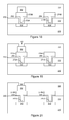
- FIG. 24 shows another embodiment. Referring to FIG. 24 , the second fill layer 292 overlies the layer 272 . Likewise, the second fill layer 292 overlies layer 272 B.
- a portion of the layer 292 covers a portion of the layer 272 .
- a portion of layer 292 may cover all of layer 272 .
- all of layer 292 may cover a portion of layer 272 .
- all of layer 292 may cover all of layer 272 .
- at least a portion of layer 292 may cover at least a portion of layer 272 .
- the opening 282 may be formed within the masking layer 280 so that it exposes a portion of the layer 272 (or a portion of layer 272 B) and a portion of the seed layer 250 ).
- FIG. 22 shows that the second fill layer 292 may be formed within the opening 282 .
- FIG. 23 shows that the masking layer 280 may be removed.
- FIG. 24 shows that a portion of the seed layer 250 may be removed so that layer ( 292 , 272 ) is electrically isolated from layer 274 .
- the layer 210 may represent a substrate (such as a semiconductor substrate).
- the substrate may include conductive regions 212 .
- FIG. 25 shows that, in or more embodiments, the layer 210 may comprise a layer 216 overlying a layer 214 .
- Layer 214 may represent a substrate such as a semiconductor substrate.
- the layer 210 may represent a layer 216 over a substrate 214 .
- the layer 216 may itself include one or more metallization levels.
- the conductive regions 212 may, for example, represent metal lines of a metallization level.
- a substrate may be a semiconductor substrate such as a bulk-semiconductor substrate or an SOI substrate (e.g. a semiconductor on insulator substrate).
- the bulk-semiconductor substrate may be a bulk-silicon substrate.
- the SOI substrate may be a silicon on insulator substrate.
- first fill layers 272 , 274 without using first masking layer 260 (and without openings 262 , 264 ).
- second fill layer 292 without using second masking layer 280 (and without opening 282 ).
- FIGS. 26A through 26F show a process for making a semiconductor structure in accordance with embodiments of the invention.
- the openings 222 , 224 as shown in FIG. 2 need not be formed.
- FIG. 26A shows a workpiece 1215 .
- Workpiece 1215 may correspond to any workpiece. In one or more embodiments, the workpiece 1215 may be different from workpiece 205 shown in FIG. 1 . In one or more embodiments, the workpiece 1215 may correspond to workpiece 205 . In one or more embodiments, the workpiece 1215 may correspond to layer 210 . In one or more embodiments, the workpiece 1215 may correspond to some other workpiece.
- the workpiece 1215 includes a top surface 1215 T.
- a barrier layer 230 may be disposed over the workpiece 1205 (e.g. over the top surface 205 T of the workpiece 1205 ).
- the barrier layer 230 may be a dielectric barrier layer.
- the barrier layer 230 may be disposed directly on the workpiece 1215 .
- An opening 232 may be formed through the dielectric barrier layer 230 . This may be done through by using masking layer (for example, a photoresist layer) and a dry etch process (similar to that shown in FIG. 6 ).
- FIG. 26B shows a seed layer 250 formed over the barrier layer 230 and within the opening 232 .
- the seed layer 250 may be is direct contact with the workpiece 1215 .
- FIG. 26C shows that a masking layer 260 (for example, a photoresist layer) may be formed over the seed layer 230 and may be patterned to from openings 262 , 264 .
- FIG. 26C also shows that first fill layers 272 , 274 may be electroplated onto the seed layer 250 within the patterned openings 262 , 264 .
- FIG. 26D shows that a masking layer 280 (for example, a photoresist layer) may be formed over the structure shown in FIG. 26C .
- the masking layer 280 may be patterned to form openings 282 , 284 .
- 26D also shows that second fill layers 292 , 294 may be electroplated onto the first fill layers 272 , 274 , respectively.
- FIG. 26E shows the removal of the masking layers 260 , 280 .
- FIG. 26F shows the removal of portions of the seed layer 250 . This electrically isolates the layer ( 292 , 272 ) from the layer ( 294 , 274 ).
- the masking layer 260 may be removed prior to the deposition of masking layer 280 .
- first fill layers 272 , 274 without using first masking layer 260 (and without openings 262 , 264 ).
- second fill layers 292 , 294 without using second masking layer 280 (and without openings 282 , 284 ).
- the workpiece 1215 may represent a substrate (such as a semiconductor substrate).
- the substrate may include conductive regions 212 .
- the workpiece 1215 may comprise a layer 216 overlying a layer 214 .
- Layer 214 may represent a substrate such as a semiconductor substrate.
- the workpiece 1215 may represent a layer 216 over a substrate 214 .
- the layer 216 may itself include one or more metallization levels.
- the conductive regions 212 may, for example, represent metal lines of a metallization level.
- all of the concepts described above may be useful for the formation of a final or top metallization level and for the formation of final or top metal lines of a semiconductor chip or integrated circuit.
- the discussion is applicable to the metallization layer of any metallization level of a semiconductor structure.
- the semiconductor structure may represent semiconductor chip and/or integrated circuit and/or a semiconductor device.
- metallization levels may, for example, be referred to as Metal-1, Metal-2, and so on.
- the seed layer 250 , the first fill layers 272 , 274 , the second fill layers 292 , 294 , the layer 212 may each be conductive layers. One or more of these layers may be metallic layers.
- the seed layer 250 , the first fill layers 272 , 274 , the second fill layers 292 , 294 , the layer 212 may include one or more conductive materials.
- a conductive material may be a metallic material.
- the metallic material may, for example, be a metal, alloy or compound.
- the metallic material may comprise one or more periodic table chemical elements from the group consisting of Cu (copper), Au (gold), Ag (silver), Al (aluminum), and W (tungsten).
- the seed layer 250 , the first fill layers 272 , 274 , the second fill layers 292 , 294 , conductive layers 212 may include one or more materials from the group consisting of copper metal, gold metal, silver metal, aluminum metal, tungsten metal, titanium metal, tantalum metal, copper alloy, gold alloy, silver alloy, aluminum alloy, tungsten alloy, titanium alloy, tantalum alloy, titanium nitride, tantalum nitride, and tungsten nitride. Combinations or mixtures of materials may also be used.
- one or more of the layers may be formed as a homogeneous layer.
- One or more of the layers may itself be formed as a stack of layer including two or more sub-layers. Two or more of the sub-layers may include different materials.
- one or more of the conductive layers described above may include non-metallic conductive materials such as doped silicon.
- the doped silicon may, for example, be doped polysilicon or doped monocrystalline silicon.
- the first fill layers 272 , 274 as well as the second fill layers 292 , 294 may include copper metal and/or copper alloy.
- the seed layer 250 may include copper metal and/or copper alloy.
- the first fill layers 272 , 274 as well as the second fill layers 292 , 294 may comprise any electroplatable material.
- a semiconductor structure e.g. a semiconductor chip and/or integrated circuit and/or semiconductor device
- a metallization layer comprising a plurality of metal lines having a plurality of thicknesses.
- the metal lines may all be spacedly disposed from each other.
- the metal lines may all be electrically isolated from each other.
- the final metal layer may include a plurality of metal lines having the same thickness.
- the metallization layer may be a final or top metal layer.
- the metal lines may be final or top metal lines.
- the metal lines (such as final metal lines) as described herein may have any widths.
- the thicker metal lines may have a wider width than a thinner line. However, this does not have to be the case. It may also be possible that a thicker line be narrower than a thinner line.
- the metallization level (such as final or top metallization level) may have at least one thicker metal line and at least one thinner metal line. In one or more embodiments, there may be at least two thicker metal lines. In one or more embodiments, there may be at least one thin metal line. The thicker and thinner metals may all be spacedly disposed from each other. The thicker and thinner metal lines may all be electrically isolated from each other.
- a semiconductor device and/or a semiconductor chip and/or a semiconductor structure having a metallization layer (such as a final or top metallization level) with a plurality of metal lines (such as final or top metal lines) with a plurality of thicknesses (for example, with both thicker and thinner metal lines) may have many applications.
- semiconductor devices and chips in Smart Power technologies may include DMOS transistors which require relatively thick metal lines (such as final metal lines). Such lines may require a relatively wide pitch (distance between lines).
- the same semiconductor devices and chips may include logic applications which require a metallization system with a relatively fine or narrow pitch. For the logic applications, thinner metal lines (such as thinner final metal lines) may be better suited so as to accommodate a finer pitch.
- One or more embodiments relate to a method for forming a semiconductor structure, comprising: providing a workpiece; forming a dielectric barrier layer over the workpiece; forming an opening through the dielectric barrier layer; forming a seed layer over the dielectric barrier layer and within the dielectric barrier layer opening; and electroplating a first fill layer on the seed layer.
- the workpiece may include an opening.
- the dielectric barrier layer may be formed within the workpiece opening.
- One or more embodiments relate to a method for forming a semiconductor structure, comprising: providing a workpiece; forming a dielectric barrier layer over the workpiece; forming an opening through the dielectric barrier layer; forming a seed layer over the dielectric barrier layer and within the dielectric barrier layer opening; and electroplating a first fill layer on the seed layer.
- One or more embodiments relate to a method for forming a semiconductor structure, comprising: providing a workpiece; forming a dielectric barrier layer over the workpiece; forming an opening through the dielectric barrier layer; forming a seed layer over the dielectric barrier layer and within the dielectric barrier layer opening; forming a first masking layer over the seed layer and forming an opening through the first masking layer to expose the seed layer; electroplating a first fill layer on the seed layer within the first masking layer opening; forming a second masking layer over the first fill layer and forming an opening through the second masking layer to expose the first fill layer; and electroplating a second fill layer on the first fill layer within the second masking layer opening.
- One or more embodiments relate to a semiconductor structure, comprising: a workpiece; a dielectric barrier layer overlying the workpiece, the dielectric barrier layer including a opening therethrough; a seed layer overlying the dielectric barrier layer and disposed within the dielectric barrier layer opening; and a first fill layer overlying the seed layer.
Abstract
One or more embodiments relate to a method for forming a semiconductor structure, comprising: providing a workpiece; forming a dielectric barrier layer over the workpiece; forming an opening through the dielectric barrier layer; forming a seed layer over the dielectric barrier layer and within the dielectric barrier layer opening; and electroplating a first fill layer on the seed layer.
Description
- This patent application is a continuation of U.S. patent application Ser. No. 12/894,189. U.S. patent application Ser. No. 12/894,189 is hereby incorporated by reference herein.
- One or more embodiments relates to semiconductor structure and methods for making semiconductor structures.
- Chips in certain technologies may include electronic devices and circuits that may require metallization having various thickness and/or widths. New ways of making metallization are needed.
-
FIGS. 1 through 20 show a method for making a semiconductor structure in accordance with an embodiment of the present invention; -
FIGS. 21 through 24 show a method for making a semiconductor structure in accordance with an embodiment of the present invention; -
FIG. 25 shows a semiconductor structure in accordance with an embodiment of the present invention; and -
FIGS. 26A through 26F show a method for making a semiconductor structure in accordance with an embodiment of the present invention; -
FIG. 26G shows a semiconductor structure in accordance with an embodiment of the present invention; and -
FIG. 26H shows a semiconductor structure in accordance with an embodiment of the present invention. - The following detailed description refers to the accompanying drawings that show, by way of illustration, specific details and embodiments in which the invention may be practiced. These embodiments are described in sufficient detail to enable those skilled in the art to practice the invention. Other embodiments may be utilized and structural, logical, and electrical changes may be made without departing from the scope of the invention. The various embodiments are not necessarily mutually exclusive, as some embodiments can be combined with one or more other embodiments to form new embodiments.
-
FIG. 1 shows aworkpiece 205. In one or more embodiments, theworkpiece 205 may be a homogeneous layer. In one or more embodiments, theworkpiece 205 may include or may be a dielectric layer. In one or more embodiments, theworkpiece 205 may comprise a dielectric material. In one or more embodiments, theworkpiece 205 may include two or more sub-layers of different materials. In one or more embodiments, theworkpiece 205 may include a substrate such as a semiconductor substrate. - Referring to
FIG. 2 ,openings workpiece 205 so that theworkpiece 205 includes theopenings openings workpiece 205 may include one or more openings. - Referring to
FIG. 3 , in one or more embodiments, theworkpiece 205 may comprise alayer 210 and alayer 220 overlying thelayer 210. - In one or more embodiments, the
layer 210 may includeconductive regions 212. In one or more embodiments, thelayer 220 may be a dielectric layer. Thedielectric layer 220 may comprise one or more dielectric materials selected from the group consisting of oxide, nitride, oxynitride. The dielectric layer may include mixtures and combinations of materials. - In one or more embodiments, the
openings layer 220. Referring toFIG. 3 , in one or more embodiments, theopenings layer 210. Theopening 222 may include abottom surface 222B and at least onesidewall surface 222S. The opening 224 may include abottom surface 224S and at least onesidewall surface 224S. In one or more embodiments, theopenings openings openings conductive regions 212. - Referring to
FIG. 4 , abarrier layer 230 may be formed over thelayer 220 and withinopenings barrier layer 230 may be formed over the sidewall and bottom surfaces of each of theopenings barrier layer 230 may be formed directly on thelayer 220 and directly on the sidewall and bottom surfaces ofopenings barrier layer 230 may be formed by a deposition process such as by a substantially conformal deposition process. Thebarrier layer 230 may be a dielectric barrier layer. In one or more embodiments, thebarrier layer 230 may comprise an oxide, a nitride and/or an oxynitride. Thebarrier layer 230 may, for example, comprise one or more material selected from the group consisting of silicon dioxide, silicon nitride, a silicon oxynitride, and combinations thereof. In one or more embodiments, thebarrier layer 230 may comprise one or more materials selected from the group consisting of SiN, SiON, SiC, SiO, SiO2, and combinations thereof. In one or more embodiments, thedielectric barrier layer 230 may include a silicon nitride material such as an HDP-silicon nitride or a UV-silicon nitride. In one or more embodiments, thebarrier layer 230 may be a homogeneous layer. In one or more embodiments, thebarrier layer 230 may comprise a combination or mixture of two or more dielectric materials. In one or more embodiments, thebarrier layer 230 may comprise two or more sub-layers of different materials. - Referring to
FIG. 5 , amasking layer 240 may be formed over thebarrier layer 230. Themasking layer layer 240 may be formed within theopenings - Referring to
FIG. 6 , themasking layer 240 may be patterned so as to formopenings masking layer 240 so as to expose thebarrier layer 230.Opening 242 is formed within opening 222 while the opening 244 is formed within opening 224. In one or more embodiments, theopenings openings masking layer 240 may be a photoresist layer. In one or more embodiments, the photoresist may comprise a galvanic photoresist. - Referring to
FIG. 7 , the patternedmasking layer 240 is used as a mask to etch thebarrier layer 230 andform openings barrier layer 230. Theopening FIG. 2 ) ofopenings layer 210, theopenings conductive regions 212 of layer 210). - Referring to
FIG. 8 , themasking layer 240 fromFIG. 7 may then be removed. This leaves the structure shown inFIG. 8 . - Referring to
FIG. 9 , aseed layer 250 may then be formed over thebarrier layer 230. In one or more embodiments, theseed layer 250 may be a conductive layer such as a metallic layer. Theseed layer 250 may formed within theopenings seed layer 250 may be formed within theopenings barrier layer 230. Theseed layer 250 may make electrical contact with thelayer 210. In one or more embodiments, theseed layer 250 may make direct contact with thelayer 210. Theseed layer 250 may be formed by a deposition process. The deposition process may be a substantially conformal deposition process. The seed layer may be formed by a chemical vapor deposition process or a physical vapor deposition process. - Referring to
FIG. 10 , amasking layer 260 may then be deposited over theseed layer 250. Themasking layer 260 may be formed within theopenings masking layer 260 may be a photoresist layer. The photoresist layer may comprise a galvanic photoresist. - Referring to
FIG. 11 , themasking layer 260 may then be patterned by removing one or more portions of themasking layer 260. The patterning of themasking layer 260 createsopenings openings opening 262 includes anupper portion 262B and alower portion 262A. Likewise, theopening 264 includes anupper portion 264B and alower portion 264A. Thelower portions openings lower portions upper portions upper portions lower portions upper portions lower portions upper portions lower portions upper portions lower portions - Referring to
FIG. 12 , first fill layers 272, 274 are formed withinopenings openings openings seed layer 230. - Referring to
FIG. 12 , each of the first fill layers 272, 274 may include alower portion 272A and anupper portion 272B. For example, thefirst fill layer 272 includes alower portion 272A formed within thelower portion 262A ofopening 262 and anupper portion 272B formed within theupper portion 262B ofopening 262. Likewise, thefirst fill layer 274 includes alower portion 274A formed within thelower portion 264A ofopening 264 and anupper portion 274B formed within theupper portion 264B ofopening 264. - Referring to
FIG. 13 , amasking layer 280 may be deposited over the structure shown inFIG. 12 to form the structure shown inFIG. 13 . Themasking layer 280 may be formed over the remaining portions of maskinglayer 260 as well as the first fill layers 272,274. In another embodiment, it is possible that themasking layer 260 is removed prior to the deposition of themasking layer 280. In one or more embodiments, themasking layer 280 may be a photoresist layer. In one or more embodiments, the photoresist layer may include a galvanic photoresist. - Referring to
FIG. 14 , themasking layer 280 may be patterned such that anopening 282 may be formed over thefirst fill layer 272. Theopening 282 may be formed so as to expose thefirst fill layer 272. Theopening 282 may be a trench or a hole. In the embodiment shown, an opening is not formed over thefirst fill layer 274. However, in another embodiment, another opening may be formed over thefirst fill layer 274. - In one or more embodiments, the
masking layer 280 and/or themasking layer 260 and/or themasking layer 240 may comprise a galvanic resist. - Referring to
FIG. 15 , asecond fill layer 292 may be formed within theopening 282 and over thefirst fill layer 272. Thesecond fill layer 292 may be a conductive layer such as a metallic layer. Thesecond fill layer 292 may be in electrical contact with thefirst fill layer 272. In one or more embodiments, thesecond fill layer 292 may be in direct contact with thefirst fill layer 272. Thesecond fill layer 292 may be formed by a deposition process. The deposition process may be an electroplating process. Hence, in one or more embodiments, thesecond fill layer 292 may be deposited by an electroplating process such that thesecond fill layer 292 is electroplated onto thefirst fill layer 272. - Referring to
FIG. 16 , themasking layer 280 and themasking layer 260 may both be removed. Removal may be accomplished by an etching process. The etching process may comprise a wet etching process. In one or more embodiments, the removal process may include a plasma strip or plasma etching process. - Referring to
FIG. 17 , the exposed portions of theseed layer 250 may be removed. The exposed portions may include those portions not underlying the first fill layers 272, 274 or thesecond fill layer 292. Removing the exposed portions of theseed layer 250 may serve to electrically isolate thelayers layer 274. In other embodiments, it may be possible that the seed layer is allowed to remain as shown inFIG. 16 . - As described herein, a layer (A, B, C) refers to the combination of layer A, layer B and layer C. For example, referring to
FIG. 17 , layer (292, 272B, 272A) refers to the combination oflayer 292,layer 272B andlayer 272A. It is noted that eachportion layer 272 may be referred to as alayer 272A and alayer 272B. Feature (292, 272B) refers to the combination oflayer 292 andlayer 272B. The layer (274B, 274A) refers to the combination oflayer 274B andlayer 274A. - A semiconductor structure, such as a semiconductor chip or integrated circuit may include one or more metallization levels. A metallization level may, for example, be metal-1, metal-2, metal-3, etc. Likewise, the metallization level may be the final or top metallization level.
- A metallization level may include one or more spacedly disposed conductive portions. For example, a metallization level may include two or more spacedly disposed portions. In some embodiments, one conductive portion may be electrical isolated from another conductive portion.
- A metallization level may include one or more metal lines. A metal line may have any shape. A metallization level may include at least one metal line. A metallization level may include two or more spaced apart metal lines. Two or more metal lines of a metallization level may be electrically isolated from each other. In some embodiments, metal line may be useful for directing electrical signals primarily in a horizontal direction.
- A metal line may include a pad structure. The pad structure may be referred to as a bond pad, a contact pad and/or a landing pad.
- Referring to
FIG. 17 , it is possible that thelayers FIG. 17 , the layer (292, 272B) may represent a first metal line of a metallization level. Likewise,layer 274B may represent a second metal line belonging to the same metallization level. The layer (292, 272B) may have a thickness T1 and a width W1. Thelayer 274B may have a thickness T2 and a width W2. In one or more embodiments, the thickness T1 may be greater than the thickness T2. In one or more embodiments, the width W1 may be greater than the width W2. Hence, in one or more embodiments, a metallization level may be formed (such as a final metallization level) that includes at least two metal lines having different thicknesses and/or different widths. - In some embodiments, it is possible that
layer 272B may represent a metal line whilelayer 292 may represent a bond pad that overlies ametal line 272B. In some embodiments, it is possible thatlayer 272B represents a metal line whilelayer 292 represents an under-bump metallization. - In some embodiments,
layer 272A andlayer 274A may, for example, represent conductive vias. A conductive via may couple one metallization level to another metallization level. A conductive via may couple a metallization level (such as metal-1) to a substrate. A conductive via that electrically couples a metallization level to a substrate may be referred to as a conductive contact. In some embodiments, conductive vias (or conductive contacts) may be useful for directing electrically signals in a substantially vertical direction. - Referring to
FIG. 18 , adielectric layer 320 may be formed over the structure shown inFIG. 17 to form the structure shown inFIG. 18 . Thedielectric layer 320 may be formed over the layer (292, 272B) andlayer 274B. In some embodiments, thedielectric layer 320 may serve as a passivation layer. - In one embodiment, the
dielectric layer 320 may comprise an imide such as a polyimide. In other embodiments, thedielectric layer 320 may comprise an oxide, a nitride or an oxynitride. Thedielectric layer 320 may, for example, be formed of silicon dioxide, silicon nitride, a silicon oxynitride or combinations thereof. In one or more embodiments, thedielectric layer 320 may comprise one or more materials selected from the group consisting of SiN, SiON, SiC, SiO, SiO2, and combinations thereof. - Referring to
FIG. 19 , anopening 322 may, optionally, be formed in thedielectric layer 320. Theopenings 322 may expose top surface oflayer 292. - Referring to
FIG. 20 , alayer 330 may then be disposed within theopening 322 and on top of the exposed metallic material oflayer 292. Thelayer 330 may comprise a metallic material. In some embodiments, thelayer 330 may be a homogeneous layer of a metallic material. Thelayer 330 may be a stack including two or more sub-layers of different materials. For example, the material may include two layers such as NiP/Pd (a Pd layer over a NiP layer) or NiMoP/Pd (a Pd layer over a NiMoP layer). As another example, the material may include three layers such as NiP/Pd/Au (an Au layer over a Pd layer over a NiP layer) or NiMoP/Pd/Au (an Au layer over a NiMoP layer over a NiMoP layer). It is possible that more than three layers be used. Thelayer 330 may serve as a pad structure when, for example, the layer (292, 272B) may serve as a final metal line. Thelayer 330 may serve as an additional pad structure when, for example, thelayer 272B represents a final metal line and thelayer 292 serves as a bond pad overlying thefinal metal line 272B. -
FIG. 24 shows another embodiment. Referring toFIG. 24 , thesecond fill layer 292 overlies thelayer 272. Likewise, thesecond fill layer 292 overlieslayer 272B. - In the embodiment shown in
FIG. 24 , a portion of thelayer 292 covers a portion of thelayer 272. In one or more embodiments, a portion oflayer 292 may cover all oflayer 272. In one or more embodiments, all oflayer 292 may cover a portion oflayer 272. In one or more embodiments, all oflayer 292 may cover all oflayer 272. Hence, in one or more embodiments, at least a portion oflayer 292 may cover at least a portion oflayer 272. - Referring to
FIG. 21 , it is seen that, in one or more embodiments, theopening 282 may be formed within themasking layer 280 so that it exposes a portion of the layer 272 (or a portion oflayer 272B) and a portion of the seed layer 250). -
FIG. 22 shows that thesecond fill layer 292 may be formed within theopening 282. -
FIG. 23 shows that themasking layer 280 may be removed. -
FIG. 24 shows that a portion of theseed layer 250 may be removed so that layer (292, 272) is electrically isolated fromlayer 274. - Referring to
FIG. 24 , in one or more embodiments, it is possible that thelayer 210 may represent a substrate (such as a semiconductor substrate). The substrate may includeconductive regions 212. -
FIG. 25 shows that, in or more embodiments, thelayer 210 may comprise alayer 216 overlying alayer 214.Layer 214 may represent a substrate such as a semiconductor substrate. Hence, thelayer 210 may represent alayer 216 over asubstrate 214. Thelayer 216 may itself include one or more metallization levels. Theconductive regions 212 may, for example, represent metal lines of a metallization level. - It is noted that a substrate may be a semiconductor substrate such as a bulk-semiconductor substrate or an SOI substrate (e.g. a semiconductor on insulator substrate). The bulk-semiconductor substrate may be a bulk-silicon substrate. The SOI substrate may be a silicon on insulator substrate.
- Referring again to
FIGS. 1 through 15 , additional embodiments of the invention may be described. For example, in some embodiments, it may be possible to electroplate first fill layers 272, 274 without using first masking layer 260 (and withoutopenings 262, 264). Likewise, in some embodiments, it may be possible to electroplatesecond fill layer 292 without using second masking layer 280 (and without opening 282). - Referring to
FIG. 15 , in another embodiment, it may be possible to removemasking layer 260 before forming themasking layer 280. -
FIGS. 26A through 26F show a process for making a semiconductor structure in accordance with embodiments of the invention. In this embodiment, theopenings FIG. 2 need not be formed.FIG. 26A shows aworkpiece 1215.Workpiece 1215 may correspond to any workpiece. In one or more embodiments, theworkpiece 1215 may be different fromworkpiece 205 shown inFIG. 1 . In one or more embodiments, theworkpiece 1215 may correspond toworkpiece 205. In one or more embodiments, theworkpiece 1215 may correspond tolayer 210. In one or more embodiments, theworkpiece 1215 may correspond to some other workpiece. - The
workpiece 1215 includes a top surface 1215T. Abarrier layer 230 may be disposed over the workpiece 1205 (e.g. over the top surface 205T of the workpiece 1205). In one or more embodiments, thebarrier layer 230 may be a dielectric barrier layer. In one or more embodiments, thebarrier layer 230 may be disposed directly on theworkpiece 1215. Anopening 232 may be formed through thedielectric barrier layer 230. This may be done through by using masking layer (for example, a photoresist layer) and a dry etch process (similar to that shown inFIG. 6 ).FIG. 26B shows aseed layer 250 formed over thebarrier layer 230 and within theopening 232. Theseed layer 250 may be is direct contact with theworkpiece 1215.FIG. 26C shows that a masking layer 260 (for example, a photoresist layer) may be formed over theseed layer 230 and may be patterned to fromopenings FIG. 26C also shows that first fill layers 272, 274 may be electroplated onto theseed layer 250 within the patternedopenings FIG. 26D shows that a masking layer 280 (for example, a photoresist layer) may be formed over the structure shown inFIG. 26C . Themasking layer 280 may be patterned to formopenings FIG. 26D also shows that second fill layers 292, 294 may be electroplated onto the first fill layers 272, 274, respectively.FIG. 26E shows the removal of the masking layers 260, 280.FIG. 26F shows the removal of portions of theseed layer 250. This electrically isolates the layer (292, 272) from the layer (294, 274). In another embodiment, it is possible that themasking layer 260 may be removed prior to the deposition ofmasking layer 280. - Referring again to
FIGS. 26A through 26F , additional embodiments of the invention may be described. For example, in some embodiments, it may be possible to electroplate first fill layers 272, 274 without using first masking layer 260 (and withoutopenings 262, 264). Likewise, in some embodiments, it may be possible to electroplate second fill layers 292, 294 without using second masking layer 280 (and withoutopenings 282, 284). - Referring to
FIG. 26G , in one or more embodiments, it is possible that theworkpiece 1215 may represent a substrate (such as a semiconductor substrate). The substrate may includeconductive regions 212. - Referring to
FIG. 26H , in or more embodiments, theworkpiece 1215 may comprise alayer 216 overlying alayer 214.Layer 214 may represent a substrate such as a semiconductor substrate. Hence, theworkpiece 1215 may represent alayer 216 over asubstrate 214. Thelayer 216 may itself include one or more metallization levels. Theconductive regions 212 may, for example, represent metal lines of a metallization level. - In one or more embodiments, all of the concepts described above may be useful for the formation of a final or top metallization level and for the formation of final or top metal lines of a semiconductor chip or integrated circuit. However, it is understood that the discussion is applicable to the metallization layer of any metallization level of a semiconductor structure. The semiconductor structure may represent semiconductor chip and/or integrated circuit and/or a semiconductor device. In one or more embodiments, metallization levels may, for example, be referred to as Metal-1, Metal-2, and so on.
- The
seed layer 250, the first fill layers 272, 274, the second fill layers 292, 294, thelayer 212 may each be conductive layers. One or more of these layers may be metallic layers. Theseed layer 250, the first fill layers 272, 274, the second fill layers 292, 294, thelayer 212 may include one or more conductive materials. A conductive material may be a metallic material. The metallic material may, for example, be a metal, alloy or compound. In one or more embodiments, the metallic material may comprise one or more periodic table chemical elements from the group consisting of Cu (copper), Au (gold), Ag (silver), Al (aluminum), and W (tungsten). - The
seed layer 250, the first fill layers 272, 274, the second fill layers 292, 294, conductive layers 212 (as well as any other conductive layer) may include one or more materials from the group consisting of copper metal, gold metal, silver metal, aluminum metal, tungsten metal, titanium metal, tantalum metal, copper alloy, gold alloy, silver alloy, aluminum alloy, tungsten alloy, titanium alloy, tantalum alloy, titanium nitride, tantalum nitride, and tungsten nitride. Combinations or mixtures of materials may also be used. In some embodiments, one or more of the layers may be formed as a homogeneous layer. One or more of the layers may itself be formed as a stack of layer including two or more sub-layers. Two or more of the sub-layers may include different materials. - In one or more embodiments, it is possible that one or more of the conductive layers described above may include non-metallic conductive materials such as doped silicon. The doped silicon may, for example, be doped polysilicon or doped monocrystalline silicon.
- In one or more embodiments, the first fill layers 272, 274 as well as the second fill layers 292, 294 may include copper metal and/or copper alloy. In one or more embodiments, the
seed layer 250 may include copper metal and/or copper alloy. In one or more embodiments, the first fill layers 272, 274 as well as the second fill layers 292, 294 may comprise any electroplatable material. - In one or more embodiments may be a semiconductor structure (e.g. a semiconductor chip and/or integrated circuit and/or semiconductor device) having a metallization layer comprising a plurality of metal lines having a plurality of thicknesses. The metal lines may all be spacedly disposed from each other. The metal lines may all be electrically isolated from each other. In one or more embodiments, the final metal layer may include a plurality of metal lines having the same thickness. The metallization layer may be a final or top metal layer. The metal lines may be final or top metal lines.
- It is noted that the metal lines (such as final metal lines) as described herein may have any widths. In one or more embodiments, the thicker metal lines may have a wider width than a thinner line. However, this does not have to be the case. It may also be possible that a thicker line be narrower than a thinner line.
- As an example, the metallization level (such as final or top metallization level) may have at least one thicker metal line and at least one thinner metal line. In one or more embodiments, there may be at least two thicker metal lines. In one or more embodiments, there may be at least one thin metal line. The thicker and thinner metals may all be spacedly disposed from each other. The thicker and thinner metal lines may all be electrically isolated from each other.
- A semiconductor device and/or a semiconductor chip and/or a semiconductor structure having a metallization layer (such as a final or top metallization level) with a plurality of metal lines (such as final or top metal lines) with a plurality of thicknesses (for example, with both thicker and thinner metal lines) may have many applications. For example, semiconductor devices and chips in Smart Power technologies may include DMOS transistors which require relatively thick metal lines (such as final metal lines). Such lines may require a relatively wide pitch (distance between lines). On the other hand, the same semiconductor devices and chips may include logic applications which require a metallization system with a relatively fine or narrow pitch. For the logic applications, thinner metal lines (such as thinner final metal lines) may be better suited so as to accommodate a finer pitch.
- One or more embodiments relate to a method for forming a semiconductor structure, comprising: providing a workpiece; forming a dielectric barrier layer over the workpiece; forming an opening through the dielectric barrier layer; forming a seed layer over the dielectric barrier layer and within the dielectric barrier layer opening; and electroplating a first fill layer on the seed layer. In one or more embodiments, the workpiece may include an opening. The dielectric barrier layer may be formed within the workpiece opening.
- One or more embodiments relate to a method for forming a semiconductor structure, comprising: providing a workpiece; forming a dielectric barrier layer over the workpiece; forming an opening through the dielectric barrier layer; forming a seed layer over the dielectric barrier layer and within the dielectric barrier layer opening; and electroplating a first fill layer on the seed layer.
- One or more embodiments relate to a method for forming a semiconductor structure, comprising: providing a workpiece; forming a dielectric barrier layer over the workpiece; forming an opening through the dielectric barrier layer; forming a seed layer over the dielectric barrier layer and within the dielectric barrier layer opening; forming a first masking layer over the seed layer and forming an opening through the first masking layer to expose the seed layer; electroplating a first fill layer on the seed layer within the first masking layer opening; forming a second masking layer over the first fill layer and forming an opening through the second masking layer to expose the first fill layer; and electroplating a second fill layer on the first fill layer within the second masking layer opening.
- One or more embodiments relate to a semiconductor structure, comprising: a workpiece; a dielectric barrier layer overlying the workpiece, the dielectric barrier layer including a opening therethrough; a seed layer overlying the dielectric barrier layer and disposed within the dielectric barrier layer opening; and a first fill layer overlying the seed layer.
- It is to be understood that the disclosure set forth herein is presented in the form of detailed embodiments described for the purpose of making a full and complete disclosure of the present invention, and that such details are not to be interpreted as limiting the true scope of this invention as set forth and defined in the appended claims.
Claims (20)
1. A method for forming a semiconductor structure, comprising:
providing a workpiece;
forming a dielectric barrier layer over said workpiece;
forming an opening through said dielectric barrier layer;
forming a seed layer over said dielectric barrier layer and within said dielectric barrier layer opening; and
electroplating a first fill layer on said seed layer.
2. The method of claim 1 , further comprising electroplating a second fill layer on said first fill layer.
3. The method of claim 1 , further comprising, after forming said seed layer and before said electroplating said first fill layer, forming a first masking layer over said seed layer and forming an opening through said first masking layer to expose said seed layer, said first fill layer being electroplated on said seed layer within said first masking layer opening.
4. The method of claim 1 , further comprising, after electroplating said first fill layer and before said electroplating said second fill layer, forming a second masking layer over said first fill layer and forming an opening through said second masking layer to expose said first fill layer, said second fill layer being electroplated on said first fill layer within said second masking layer opening.
5. The method of claim 3 , further comprising, after electroplating said first fill layer and before said electroplating said second fill layer, forming a second masking layer over said first fill layer and forming an opening through said second masking layer to expose said first fill layer, said second fill layer being electroplated on said first fill layer within said second masking layer opening.
6. The method of claim 1 , wherein said first fill layer and/or said seed layer comprises Cu (copper).
7. The method of claim 1 , wherein said dielectric barrier layer comprises an oxide, a nitride and/or an oxynitride.
8. The method of claim 2 , wherein said second fill layer comprises Cu (copper).
9. The method of claim 1 , wherein said workpiece includes an opening, said barrier layer formed within said workpiece opening, said barrier layer opening formed within said workpiece opening.
10. A method for forming a semiconductor structure, comprising:
providing a workpiece;
forming a dielectric barrier layer over said workpiece;
forming an opening through said dielectric barrier layer;
forming a seed layer over said dielectric barrier layer and within said dielectric barrier layer opening;
forming a first masking layer over said seed layer and forming an opening through said first masking layer to expose said seed layer;
electroplating a first fill layer on said seed layer within said first masking layer opening;
forming a second masking layer over said first fill layer and forming an opening through said second masking layer to expose said first fill layer; and
electroplating a second fill layer on said first fill layer within said second masking layer opening.
11. The method of claim 10 , wherein said seed layer and/or said first fill layer and/or said second fill layer comprise Cu (copper).
12. The method of claim 11 , wherein said Cu (copper) is copper metal and/or copper alloy.
13. The method of claim 10 , wherein said dielectric barrier layer comprises at least one of oxide, nitride and oxynitride.
14. The method of claim 10 , wherein said workpiece includes an opening, said barrier layer formed within said workpiece opening, said barrier layer opening formed within said workpiece opening.
15. A semiconductor structure, comprising:
a workpiece;
a dielectric barrier layer overlying said workpiece, said dielectric barrier layer including an opening therethrough;
a seed layer overlying said dielectric barrier layer and disposed within said dielectric barrier layer opening; and
a first fill layer overlying said seed layer.
16. The structure of claim 1 , further comprising a second fill layer overlying said first fill layer.
17. The structure of claim 15 , wherein said seed layer and/or said first fill layer comprises Cu (copper).
18. The structure of claim 15 , wherein said dielectric barrier layer comprises at least one of oxide, nitride and oxynitride.
19. The structure of claim 15 , wherein said workpiece includes an opening, said dielectric barrier layer disposed within said workpiece opening, said dielectric barrier layer opening disposed within said workpiece opening.
20. The structure of claim 19 , wherein said dielectric barrier layer overlies a bottom and sidewall surface of said workpiece opening.
Priority Applications (1)
| Application Number | Priority Date | Filing Date | Title |
|---|---|---|---|
| US14/060,641 US9230885B2 (en) | 2010-09-30 | 2013-10-23 | Semiconductor structure and method for making same |
Applications Claiming Priority (2)
| Application Number | Priority Date | Filing Date | Title |
|---|---|---|---|
| US12/894,189 US8580687B2 (en) | 2010-09-30 | 2010-09-30 | Semiconductor structure and method for making same |
| US14/060,641 US9230885B2 (en) | 2010-09-30 | 2013-10-23 | Semiconductor structure and method for making same |
Related Parent Applications (1)
| Application Number | Title | Priority Date | Filing Date |
|---|---|---|---|
| US12/894,189 Continuation US8580687B2 (en) | 2010-09-30 | 2010-09-30 | Semiconductor structure and method for making same |
Publications (2)
| Publication Number | Publication Date |
|---|---|
| US20140077379A1 true US20140077379A1 (en) | 2014-03-20 |
| US9230885B2 US9230885B2 (en) | 2016-01-05 |
Family
ID=45832650
Family Applications (2)
| Application Number | Title | Priority Date | Filing Date |
|---|---|---|---|
| US12/894,189 Active US8580687B2 (en) | 2010-09-30 | 2010-09-30 | Semiconductor structure and method for making same |
| US14/060,641 Active US9230885B2 (en) | 2010-09-30 | 2013-10-23 | Semiconductor structure and method for making same |
Family Applications Before (1)
| Application Number | Title | Priority Date | Filing Date |
|---|---|---|---|
| US12/894,189 Active US8580687B2 (en) | 2010-09-30 | 2010-09-30 | Semiconductor structure and method for making same |
Country Status (2)
| Country | Link |
|---|---|
| US (2) | US8580687B2 (en) |
| DE (1) | DE102011053356A1 (en) |
Cited By (3)
| Publication number | Priority date | Publication date | Assignee | Title |
|---|---|---|---|---|
| US10002789B2 (en) | 2016-03-24 | 2018-06-19 | International Business Machines Corporation | High performance middle of line interconnects |
| US20200126926A1 (en) * | 2018-10-19 | 2020-04-23 | International Business Machines Corporation | Middle-of-line interconnect having low metal-to-metal interface resistance |
| US10903111B2 (en) | 2019-03-20 | 2021-01-26 | International Business Machines Corporation | Semiconductor device with linerless contacts |
Families Citing this family (8)
| Publication number | Priority date | Publication date | Assignee | Title |
|---|---|---|---|---|
| US20090079080A1 (en) * | 2007-09-24 | 2009-03-26 | Infineon Technologies Ag | Semiconductor Device with Multi-Layer Metallization |
| CN103000515B (en) * | 2011-09-14 | 2015-07-08 | 中芯国际集成电路制造(北京)有限公司 | Semiconductor device and manufacturing method thereof |
| US10083893B2 (en) * | 2014-01-30 | 2018-09-25 | Toshiba Memory Corporation | Semiconductor device and semiconductor device manufacturing method |
| TW201545215A (en) * | 2014-05-28 | 2015-12-01 | Touch Crporation J | Method of manufacturing microstructures of metal lines |
| US9368436B2 (en) * | 2014-08-04 | 2016-06-14 | Infineon Technologies Ag | Source down semiconductor devices and methods of formation thereof |
| US9761548B1 (en) * | 2016-05-19 | 2017-09-12 | Infineon Technologies Ag | Bond pad structure |
| US10340206B2 (en) | 2016-08-05 | 2019-07-02 | Taiwan Semiconductor Manufacturing Company, Ltd. | Dense redistribution layers in semiconductor packages and methods of forming the same |
| US20220157655A1 (en) * | 2020-11-19 | 2022-05-19 | Applied Materials, Inc. | Electroplating with temporary features |
Citations (7)
| Publication number | Priority date | Publication date | Assignee | Title |
|---|---|---|---|---|
| US5674787A (en) * | 1996-01-16 | 1997-10-07 | Sematech, Inc. | Selective electroless copper deposited interconnect plugs for ULSI applications |
| US6150723A (en) * | 1997-09-30 | 2000-11-21 | International Business Machines Corporation | Copper stud structure with refractory metal liner |
| US6153521A (en) * | 1998-06-04 | 2000-11-28 | Advanced Micro Devices, Inc. | Metallized interconnection structure and method of making the same |
| US20010027019A1 (en) * | 2000-04-04 | 2001-10-04 | Hiromu Ishii | Pattern forming method |
| US6624066B2 (en) * | 2001-02-14 | 2003-09-23 | Texas Instruments Incorporated | Reliable interconnects with low via/contact resistance |
| US20060194430A1 (en) * | 2005-02-28 | 2006-08-31 | Michael Beck | Metal interconnect structure and method |
| US20100078825A1 (en) * | 2008-09-29 | 2010-04-01 | Ryan James Patz | Method for fabricating interconnect structures for semiconductor devices |
Family Cites Families (6)
| Publication number | Priority date | Publication date | Assignee | Title |
|---|---|---|---|---|
| US6555461B1 (en) | 2001-06-20 | 2003-04-29 | Advanced Micro Devices, Inc. | Method of forming low resistance barrier on low k interconnect |
| US6784096B2 (en) * | 2002-09-11 | 2004-08-31 | Applied Materials, Inc. | Methods and apparatus for forming barrier layers in high aspect ratio vias |
| JP2006032864A (en) * | 2004-07-21 | 2006-02-02 | Sony Corp | Multilayer wiring structure, semiconductor device having the same, and manufacturing method thereof |
| CN100356545C (en) | 2004-09-21 | 2007-12-19 | 中芯国际集成电路制造(上海)有限公司 | Method and structure for lowering contact electric resistance in double inlay structure of semiconductor device |
| US8399989B2 (en) | 2005-07-29 | 2013-03-19 | Megica Corporation | Metal pad or metal bump over pad exposed by passivation layer |
| US20090079080A1 (en) | 2007-09-24 | 2009-03-26 | Infineon Technologies Ag | Semiconductor Device with Multi-Layer Metallization |
-
2010
- 2010-09-30 US US12/894,189 patent/US8580687B2/en active Active
-
2011
- 2011-09-07 DE DE102011053356A patent/DE102011053356A1/en not_active Ceased
-
2013
- 2013-10-23 US US14/060,641 patent/US9230885B2/en active Active
Patent Citations (7)
| Publication number | Priority date | Publication date | Assignee | Title |
|---|---|---|---|---|
| US5674787A (en) * | 1996-01-16 | 1997-10-07 | Sematech, Inc. | Selective electroless copper deposited interconnect plugs for ULSI applications |
| US6150723A (en) * | 1997-09-30 | 2000-11-21 | International Business Machines Corporation | Copper stud structure with refractory metal liner |
| US6153521A (en) * | 1998-06-04 | 2000-11-28 | Advanced Micro Devices, Inc. | Metallized interconnection structure and method of making the same |
| US20010027019A1 (en) * | 2000-04-04 | 2001-10-04 | Hiromu Ishii | Pattern forming method |
| US6624066B2 (en) * | 2001-02-14 | 2003-09-23 | Texas Instruments Incorporated | Reliable interconnects with low via/contact resistance |
| US20060194430A1 (en) * | 2005-02-28 | 2006-08-31 | Michael Beck | Metal interconnect structure and method |
| US20100078825A1 (en) * | 2008-09-29 | 2010-04-01 | Ryan James Patz | Method for fabricating interconnect structures for semiconductor devices |
Cited By (6)
| Publication number | Priority date | Publication date | Assignee | Title |
|---|---|---|---|---|
| US10002789B2 (en) | 2016-03-24 | 2018-06-19 | International Business Machines Corporation | High performance middle of line interconnects |
| US10211095B2 (en) | 2016-03-24 | 2019-02-19 | International Business Machines Corporation | High performance middle of line interconnects |
| US20200126926A1 (en) * | 2018-10-19 | 2020-04-23 | International Business Machines Corporation | Middle-of-line interconnect having low metal-to-metal interface resistance |
| US11114382B2 (en) * | 2018-10-19 | 2021-09-07 | International Business Machines Corporation | Middle-of-line interconnect having low metal-to-metal interface resistance |
| US10903111B2 (en) | 2019-03-20 | 2021-01-26 | International Business Machines Corporation | Semiconductor device with linerless contacts |
| US11688632B2 (en) | 2019-03-20 | 2023-06-27 | International Business Machines Corporation | Semiconductor device with linerless contacts |
Also Published As
| Publication number | Publication date |
|---|---|
| US8580687B2 (en) | 2013-11-12 |
| US9230885B2 (en) | 2016-01-05 |
| DE102011053356A1 (en) | 2012-04-05 |
| US20120080795A1 (en) | 2012-04-05 |
Similar Documents
| Publication | Publication Date | Title |
|---|---|---|
| US9230885B2 (en) | Semiconductor structure and method for making same | |
| US11923338B2 (en) | Stacked integrated circuits with redistribution lines | |
| US10074584B2 (en) | Method of forming a semiconductor component comprising a second passivation layer having a first opening exposing a bond pad and a plurality of second openings exposing a top surface of an underlying first passivation layer | |
| US8319343B2 (en) | Routing under bond pad for the replacement of an interconnect layer | |
| US9490205B2 (en) | Integrated circuit interconnects and methods of making same | |
| US8865585B2 (en) | Method of forming post passivation interconnects | |
| US7598616B2 (en) | Interconnect structure | |
| CN101465332B (en) | Semiconductor chip, method of fabricating the same and semiconductor chip stack package | |
| KR100659801B1 (en) | Wire bonding to copper | |
| US20110254159A1 (en) | Conductive feature for semiconductor substrate and method of manufacture | |
| US7816792B2 (en) | Semiconductor device with conductive interconnect | |
| US8102051B2 (en) | Semiconductor device having an electrode and method for manufacturing the same | |
| US9627256B2 (en) | Integrated circuit interconnects and methods of making same | |
| US10290576B2 (en) | Stress reduction apparatus with an inverted cup-shaped layer | |
| US7245025B2 (en) | Low cost bonding pad and method of fabricating same | |
| US9281234B2 (en) | WLCSP interconnect apparatus and method | |
| KR100691051B1 (en) | Dual damascene bond pad structure for lowering stress and allowing circuitry under pads and a process to form the same | |
| US6974770B2 (en) | Self-aligned mask to reduce cell layout area | |
| US11355464B2 (en) | Semiconductor device structure with bottle-shaped through silicon via and method for forming the same | |
| US20230352433A1 (en) | Semiconductor device structure with composite bottle-shaped through silicon via and method for prepriang the same | |
| US10818625B1 (en) | Electronic device | |
| KR20090034613A (en) | Method for forming bond pad on fabricating a semiconductor device |
Legal Events
| Date | Code | Title | Description |
|---|---|---|---|
| FEPP | Fee payment procedure |
Free format text: PAYOR NUMBER ASSIGNED (ORIGINAL EVENT CODE: ASPN); ENTITY STATUS OF PATENT OWNER: LARGE ENTITY |
|
| STCF | Information on status: patent grant |
Free format text: PATENTED CASE |
|
| MAFP | Maintenance fee payment |
Free format text: PAYMENT OF MAINTENANCE FEE, 4TH YEAR, LARGE ENTITY (ORIGINAL EVENT CODE: M1551); ENTITY STATUS OF PATENT OWNER: LARGE ENTITY Year of fee payment: 4 |
|
| MAFP | Maintenance fee payment |
Free format text: PAYMENT OF MAINTENANCE FEE, 8TH YEAR, LARGE ENTITY (ORIGINAL EVENT CODE: M1552); ENTITY STATUS OF PATENT OWNER: LARGE ENTITY Year of fee payment: 8 |