US3810025A - Field emission type electron gun - Google Patents
Field emission type electron gun Download PDFInfo
- Publication number
- US3810025A US3810025A US00245232A US24523272A US3810025A US 3810025 A US3810025 A US 3810025A US 00245232 A US00245232 A US 00245232A US 24523272 A US24523272 A US 24523272A US 3810025 A US3810025 A US 3810025A
- Authority
- US
- United States
- Prior art keywords
- emitter
- electrode
- transformer
- voltage
- circuit
- Prior art date
- Legal status (The legal status is an assumption and is not a legal conclusion. Google has not performed a legal analysis and makes no representation as to the accuracy of the status listed.)
- Expired - Lifetime
Links
Images


Classifications
-
- H—ELECTRICITY
- H01—ELECTRIC ELEMENTS
- H01J—ELECTRIC DISCHARGE TUBES OR DISCHARGE LAMPS
- H01J37/00—Discharge tubes with provision for introducing objects or material to be exposed to the discharge, e.g. for the purpose of examination or processing thereof
- H01J37/02—Details
- H01J37/24—Circuit arrangements not adapted to a particular application of the tube and not otherwise provided for
- H01J37/241—High voltage power supply or regulation circuits
-
- H—ELECTRICITY
- H01—ELECTRIC ELEMENTS
- H01J—ELECTRIC DISCHARGE TUBES OR DISCHARGE LAMPS
- H01J3/00—Details of electron-optical or ion-optical arrangements or of ion traps common to two or more basic types of discharge tubes or lamps
- H01J3/02—Electron guns
- H01J3/021—Electron guns using a field emission, photo emission, or secondary emission electron source
-
- H—ELECTRICITY
- H01—ELECTRIC ELEMENTS
- H01J—ELECTRIC DISCHARGE TUBES OR DISCHARGE LAMPS
- H01J37/00—Discharge tubes with provision for introducing objects or material to be exposed to the discharge, e.g. for the purpose of examination or processing thereof
- H01J37/02—Details
- H01J37/04—Arrangements of electrodes and associated parts for generating or controlling the discharge, e.g. electron-optical arrangement, ion-optical arrangement
- H01J37/06—Electron sources; Electron guns
- H01J37/073—Electron guns using field emission, photo emission, or secondary emission electron sources
-
- H—ELECTRICITY
- H02—GENERATION; CONVERSION OR DISTRIBUTION OF ELECTRIC POWER
- H02H—EMERGENCY PROTECTIVE CIRCUIT ARRANGEMENTS
- H02H7/00—Emergency protective circuit arrangements specially adapted for specific types of electric machines or apparatus or for sectionalised protection of cable or line systems, and effecting automatic switching in the event of an undesired change from normal working conditions
- H02H7/20—Emergency protective circuit arrangements specially adapted for specific types of electric machines or apparatus or for sectionalised protection of cable or line systems, and effecting automatic switching in the event of an undesired change from normal working conditions for electronic equipment
Definitions
- Patent 11 1 FIELD EMISSION TYPE ELECTRON GUN Inventors: Ryuzo Aihara; Susumu Ota;
- ABSTRACT This invention relates to a field emission type electron gun capable of protecting the emitter tip from damage when electrical breakdown occurs in the gun chamber.
- the preferred embodiments incorporate circuitry for decreasing the impedance between the emitter and its associated electrode when electrical breakdown occurs.
- This invention relates to a field emission type electron gun capable of protecting the emitter tip from damage when electrical breakdown occurs in the gun chamber.
- the advantage of a field emission type electron gun in electron microscopes and the like as compared with the ordinary thermionic emission'type electron gun, is that it is possible to obtain a high current electron beam forming a microspot.
- the emitter is very easily damaged due to electrical breakdown caused by a deterioration in the gun chamber vacuum or other phenomena, resulting in the generation of an unusually strong electric field in the vicinity of the emitter tip. As a result the tip is overheated due to large current during vacuum arc discharge. This inevitably results in a change in shape in the emitter tip which then becomes useless.
- a field emission electron gun comprises a circuit for preventing an unusually high potential difference between the emitter and an electrode spaced near the emitter resulting from an electrical breakdown between that electrode and the grounded anode.
- the preferred means of preventing the unusually high potential difference is to provide a circuit between the emitter and electrode which has a reduced impedance at the time of breakdown and preferably a circuit to increase impedance between the high voltage source and the emitter when breakdown occurs.
- FIGS. 1(a) and (b) are schematic diagrams of a con- ,ventional field emission type electron gun.
- FIG. 2 is a diagrammatic circuit of one embodiment according to the invention.
- a gun chamber 1 contains a filament 2 heated by an A.C. current source 3 through an insulating'transformer 4, an emitter 5 attached to the filament 2, first electrode '6 for producing a strong electric field (for example, about lO' volt/cm) in the vicinity of the emitter tip and an anode 7 maintained at ground potentiaLA voltage source 8 supplies a voltage so as to create a constant orpulsed potential difference between the emitter 5 and the first electrode 6, in order a to draw electrons from said emitter tip.
- Another volt age source 9 maintains the emitter at a high negative DC. potential in order to accelerate the emitted electrons.
- Z10 and Z11 represent the impedances of sources 8 and 9 (FIG. 1(a)) respectively, and Z12 the impedance between the two sources.
- the protection circuit 13 is arranged in parallel with voltage supply source 8, said circuit comprising a thyratron 14, a variable DC. voltage source 15 for adjusting the firing voltage of the thyratron 14, and a coupling condenser 16.
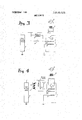
- FIG. 3 illustrates another embodiment according to this invention in which an on-off switch 17 is provided in place of protection circuit 13.
- This particular embodiment is very effective when electrical breakdown is predetermined as, for example, when applying the so-called conditioning technique whereby electrical breakdown between the first electrode and the anode is caused by setting the output voltage of voltage source 9 slightly higher than the regular working output voltage, in order to improve the withstand voltage in the gun chambenln this case, switch 17 is switched on during the conditioning" operation, and switched off during regular operation;
- FIG. 4 illustrates yet another embodiment of the invention in which an additional electrode 18, hereinafter referred to as the second electrode, is provided between the first electrode 6 andthe anode 7.
- the potential applied to the second electrode 18 is determined by a DC. voltage source 19 and the voltage source 9.
- the output voltage of the voltage source 19 is almost the same as that of source 8 if the output of source 8 is DC, and is almost the same as. the pulse height of the output of source 8 if the output of source 8 is pulse.
- the output voltage of source 19 is much smaller than the output voltage of source 9. Accordingly, electrical breakdown between the second electrode 18 and the anode 7 almost always occurs before the occurrence of breakdown between the second electrode 18 and the first electrode 6.
- protection circuit 13 comprising a silicon symmetric switch (8.8.8.) 20, thereby decreasing the impedance between the two electrodes and, in so doing, prevents the reoccurrence of electrical breakdown since the potential fluctuation of said electrodes and the emitter 5 are about the same.
- An additional advantage of this embodiment is the fact that the range of the protection circuit firing voltage is much wider than that of the protection-circuit decause, in the case of the embodiment shown in FIG. 2, it is necessary to adjust the firing voltage in accordance with the output voltage of voltage source 8 which has to be varied every time the emitter is exchanged. In the case of this embodiment, however, the relevant voltage source is source 19 which is seldom varied. Hence, in the case of this embodiment, there is almost no necessity to adjust the firing voltage of protection circuit 13. For this reason, it is possible to utilize a simple S.S.S. 20 switching device in place of the more complicated thyratron and its associated circuit.
- FIG. The embodiment illustrated in FIG. is substantially the same as that illustrated in FIG. 4.
- an insulation column 21 containing an insulating transformer 4, a high voltage source 22 and a filter circuit consisting of a resistor 23 and capacitors 24 is connected to gun chamber circuit 25 by high voltage cable 26.
- the potential at the junction of balancing resistors 27 and 28 is used instead of the potential of the emitter 5, and protection circuit 13 which, in this case, incorporates a surge voltage protection tube 29 is connected between said junction and the second electrode 18.
- this particular embodiment is very effective when electrical breakdown is predetermined as mentioned in the explanation of the embodiment shown in FIG. 3.
- FIG. 6 illustrates an embodiment designed to further reduce E by increasing the impedance Z31 during discharge in addition to decreasing the impedance Z30.
- circuit 32 consisting of a transformer 33, balancing resistors 34, 35, 36 and 37 and a high order resistor 38 capable of withstanding the high voltage output of source 22.
- the two ends of the resistor 38 are connected to the junction of resistors 36 and 37 and the junction of resistors 34 and 35, respectively.
- the embodiment When there is no discharge, the embodiment functions the same way as the embodiment shown in FIG. 5. If electrical breakdown occurs between the second electrode 18 and the anode 7, the amount. of discharge current flowing through high order resistor 38 is very much reduced, and the potential difference between the emitter 5 and the first electrode 6 is not so large.
- Voltage source 8 consisting of an A.C. voltage source 40, insulating transformer 41, a pulse generator 39, a transformer 42 and a high order resistor 43 generates a pulse voltage which is applied to electrode 6 through transformer 42.
- the discharge current due to the stray capacity of transformer 41 flows through resistor 43.
- FIG. 7 illustrates a practical embodiment of the present invention in which function and operation is substantially the same as the embodiments shown in FIGS. 5 and 6.
- pulse generator 39, insu lating transformer 41, and D.C. voltage source 19 etc. are all housed in insulation column 21.
- the potential at the center tap of the output winding of transformer-4 is used instead of the potential at center tap of the input winding of transformer 33.
- the function of resistor 44 is the same as that of resistor 43 in FIG. 6.
- FIG. 8 illustrates an embodiment for D.C. field emission operation corresponding to the embodiment shown in FIG. 7.
- the function of resistor '45 is the same as that of resistors 44 and 38.
- FIG. 9 illustrates an embodiment designed to increase the impedance 231 inductively instead of resistively as in the case of the embodiments shown in FIGS.
- circuit 32 which has a fairly high inductance; whereas, under normal operat ing conditions, the inductance of circuit 32 is cancelled out by the coils and is, therefore, zero.
- the pulse signals generated by pulse generator 39 are transmitted to the input winding of the transformer 42 and capacitor CN+1 via the transmission line consisting ofcoils L21 L2N, L31 L3N and capacitors C1 CN without loss.
- resistor 51 connected across the output winding of transformer 42 compensates for the sag in the pulse voltage applied between the emitter 5 and the first electrode 6.
- the filament heating current is D.C. rectified by rectification circuit 52. Even if A.C. current is used for heating the filament, there is practically no loss in circuit 32, because coils L11, LIN and coils L31, L3N have the same inductance and are unidirectionally wound.
- a field emission type electron gun device comprising:
- a high voltage source for supplying negative high potential to said emitter in order to accelerate said electron beam
- a voltage source for generating a potential difference between said electrode and said emitter in order to generate a strong electric field in the vicinity of said emitter tip
- a protection means for preventing the generation of an unusually high potential difference between said emitter and said electrode comprising a switching circuit for rapidly decreasing the impedance of said protection means in the event that the voltage between said emitter and said electrode increases beyond the firing voltage of the switching circuit, and
- means for heating the emitter comprising a first and second isolation transformer, the secondary of the first transformer being in series with the primaryof the second transformer, the primary of the first transformer being connected to an AC voltage supply, the secondary of the second transformer being in series with the emitter of the electron gun,
- a field emission type electron gun device comprismg:
- a high voltage source for supplying negative high potential to said emitter in order to accelerate said electron beam
- a voltage source for generating a potential diffen ence between said first electrode and said emitter in order to generate a strong electric field in the vicinity of said emitter tip
- a DC voltage source for supplying a potential to said secondary electrode
- a protection means for preventing the generation of an unusually high potential difference between said second electrode and said emitter comprising a switching circuit for rapidly decreasing the impedance of said protection means in the event that the voltage between said emitter and said second electrode increases beyond the firing voltage of the switching circuit, and
- means for heating the emitter comprising a first and second isolation transformer, the secondary of the first transformer being in series with the primary of the second transformer, the primary of the first transformer being connected to an AC. voltage supply, the secondary of the, second transformer being in series with the emitter of the electron gun, the high voltage supply being connected to the circuit between the said first and second transformers and the emitter being connected through a high value resistor to the circuit between said first and second transformers.
Abstract
This invention relates to a field emission type electron gun capable of protecting the emitter tip from damage when electrical breakdown occurs in the gun chamber. The preferred embodiments incorporate circuitry for decreasing the impedance between the emitter and its associated electrode when electrical breakdown occurs.
Description
United States Aihara et a1.
Patent 11 1 FIELD EMISSION TYPE ELECTRON GUN Inventors: Ryuzo Aihara; Susumu Ota;
Nobuyuki Kobayashi, all of Tokyo, Japan Nihon Denshi Kabushiki Kaisha, Tokyo, Japan Filed: Apr. 18, 1972 Appl. No.: 245,232
Assignee:
Foreign Application Priority Data Apr. 20, 1971 Japan 46-30876 May 11, 1971 Japan.... 46-31405 Sept. 7, 1971 Japan 46 69070 U..S. CL; 328/10, 313/336, 315/307, 7 315/310, 328/8 Int. Cl. H02h 7/20 Field of Search 315/106, 107, 175, 176, 315/307, 310, 311; 328/8-10 Refere nces Cited UNITED STATES PATENTS 8/1966 Gessford 328/10 X May 7, 1974 2,083,205 6/1937 Schlesinger 328 10'x 3,461,391 8/1969 Clerc 328/168 x 2,829,282 4/1958 Hughes et a1. 1 307/237 X 2,428,616 10/1947 Clapp 328/9 2,828,417 3/1958 Flemming et a1. 307/237 x 3,502,933 3/1970 Leimontas et a]. 328/8 x OTHER PUBLICATIONS Smith, CRT Arcing, Electra-Optical Systems Design, Nov. 1971, cover and pp. 14-18.
Primary Examiner-Rudolph V. Rolinec Assistant Examiner-Wi1liam D. 'Larkins Attorney, Agent, or Firm--W ebb, Burden, Robinson & Webb [57] ABSTRACT This invention relates to a field emission type electron gun capable of protecting the emitter tip from damage when electrical breakdown occurs in the gun chamber. The preferred embodiments incorporate circuitry for decreasing the impedance between the emitter and its associated electrode when electrical breakdown occurs.
2 Claims, 11 Drawing Figures PATENTEUIAY 7 m4 sum 1 0r 5 ACTE T SWRCE HIGH VOLTAGE SOURCE VOL van/we SOURCE PATENTEDMAY 7 m4 SHE] Z 5 VOLT/1 GE SOURCE HIGH VOL AGE SOURCE PAIENTEDMY 1 m4 3.810.025
SHEET 30$ 5 6 70 a 25 ZVQL 2 J v I 28mg: 5
Iain.
This invention relates to a field emission type electron gun capable of protecting the emitter tip from damage when electrical breakdown occurs in the gun chamber. The advantage of a field emission type electron gun in electron microscopes and the like as compared with the ordinary thermionic emission'type electron gun, is that it is possible to obtain a high current electron beam forming a microspot. Unfortunately, however, in the case of the field emission type gun, the emitter is very easily damaged due to electrical breakdown caused by a deterioration in the gun chamber vacuum or other phenomena, resulting in the generation of an unusually strong electric field in the vicinity of the emitter tip. As a result the tip is overheated due to large current during vacuum arc discharge. This inevitably results in a change in shape in the emitter tip which then becomes useless.
It is a principal object of this invention to prevent electrical breakdown from damaging the emitter tip.
Briefly, according to this invention, a field emission electron gun comprises a circuit for preventing an unusually high potential difference between the emitter and an electrode spaced near the emitter resulting from an electrical breakdown between that electrode and the grounded anode. The preferred means of preventing the unusually high potential difference is to provide a circuit between the emitter and electrode which has a reduced impedance at the time of breakdown and preferably a circuit to increase impedance between the high voltage source and the emitter when breakdown occurs.
Further features of this invention will become apparent by reading the following detailed description in conjunction with the accompanying drawings, in which:
FIGS. 1(a) and (b) are schematic diagrams ofa con- ,ventional field emission type electron gun.
FIG. 2 is a diagrammatic circuit of one embodiment according to the invention.
FIGS. 3 to show other embodiments according to this invention. a
Referring to FIG. 1(a), a gun chamber 1 contains a filament 2 heated by an A.C. current source 3 through an insulating'transformer 4, an emitter 5 attached to the filament 2, first electrode '6 for producing a strong electric field (for example, about lO' volt/cm) in the vicinity of the emitter tip and an anode 7 maintained at ground potentiaLA voltage source 8 supplies a voltage so as to create a constant orpulsed potential difference between the emitter 5 and the first electrode 6, in order a to draw electrons from said emitter tip. Another volt age source 9 maintains the emitter at a high negative DC. potential in order to accelerate the emitted electrons.
In this electron gun, electrical breakdown occurs mostly between the first electrode 6 and the anode 7, due to the high potential difference existing there compared with that existing between the first electrode 6 and the emitter 5. I
In FIG. 1(b), Z10 and Z11 represent the impedances of sources 8 and 9 (FIG. 1(a)) respectively, and Z12 the impedance between the two sources.
When electrical breakdown occurs between the first V electrode 6 and the anode 7, the potential of the first electrode 6 becomes zero (ground) and discharge cur- Referring to FIG. 2, the protection circuit 13 is arranged in parallel with voltage supply source 8, said circuit comprising a thyratron 14, a variable DC. voltage source 15 for adjusting the firing voltage of the thyratron 14, and a coupling condenser 16.
When surge voltage, resulting from electrical breakdown, is applied to circuit 13; that is to say, across source 8, the impedance of the circuit decreases, thereby protecting the emitter tip from damage due to said surge voltage.
FIG. 3 illustrates another embodiment according to this invention in which an on-off switch 17 is provided in place of protection circuit 13.
This particular embodiment is very effective when electrical breakdown is predetermined as, for example, when applying the so-called conditioning technique whereby electrical breakdown between the first electrode and the anode is caused by setting the output voltage of voltage source 9 slightly higher than the regular working output voltage, in order to improve the withstand voltage in the gun chambenln this case, switch 17 is switched on during the conditioning" operation, and switched off during regular operation;
FIG. 4 illustrates yet another embodiment of the invention in which an additional electrode 18, hereinafter referred to as the second electrode, is provided between the first electrode 6 andthe anode 7. The potential applied to the second electrode 18 is determined by a DC. voltage source 19 and the voltage source 9. In this case, the output voltage of the voltage source 19 is almost the same as that of source 8 if the output of source 8 is DC, and is almost the same as. the pulse height of the output of source 8 if the output of source 8 is pulse. Moreover, the output voltage of source 19 is much smaller than the output voltage of source 9. Accordingly, electrical breakdown between the second electrode 18 and the anode 7 almost always occurs before the occurrence of breakdown between the second electrode 18 and the first electrode 6.
The moment breakdown occurs between the second electrode 18 and the anode 7, the potential of the second electrode 18 changes from negative high potential to ground potential. As a result, the potential difference between the'second electrode 18 and the first electrode 6 increases drastically due to the sudden outflow of discharge current through the impedance of DC. voltage source 19. This, in turn, activates protection circuit 13, comprising a silicon symmetric switch (8.8.8.) 20, thereby decreasing the impedance between the two electrodes and, in so doing, prevents the reoccurrence of electrical breakdown since the potential fluctuation of said electrodes and the emitter 5 are about the same. I
An additional advantage of this embodiment is the fact that the range of the protection circuit firing voltage is much wider than that of the protection-circuit decause, in the case of the embodiment shown in FIG. 2, it is necessary to adjust the firing voltage in accordance with the output voltage of voltage source 8 which has to be varied every time the emitter is exchanged. In the case of this embodiment, however, the relevant voltage source is source 19 which is seldom varied. Hence, in the case of this embodiment, there is almost no necessity to adjust the firing voltage of protection circuit 13. For this reason, it is possible to utilize a simple S.S.S. 20 switching device in place of the more complicated thyratron and its associated circuit.
The embodiment illustrated in FIG. is substantially the same as that illustrated in FIG. 4. In this embodiment, however, an insulation column 21 containing an insulating transformer 4, a high voltage source 22 and a filter circuit consisting of a resistor 23 and capacitors 24 is connected to gun chamber circuit 25 by high voltage cable 26. Further, the potential at the junction of balancing resistors 27 and 28 is used instead of the potential of the emitter 5, and protection circuit 13 which, in this case, incorporates a surge voltage protection tube 29 is connected between said junction and the second electrode 18.
In an on-off switch is provided in place .of the protection circuit 13, this particular embodiment is very effective when electrical breakdown is predetermined as mentioned in the explanation of the embodiment shown in FIG. 3. Y
In the embodiment. shown in FIG. 5, theoretically speaking, when electrical breakdown occurs between the second electrode 18 and the anode 7, vacuum arc discharge between the emitter and the first electrode 6 does not occur. In practice, however, if the residual impedance in the protection circuit is fairly large, the potential difference between electrode 6 and electrode 18 will be correspondingly large due to the outflow of discharge current.
The peak voltage E of the potential difference is given by the following equation:
FIG. 6 illustrates an embodiment designed to further reduce E by increasing the impedance Z31 during discharge in addition to decreasing the impedance Z30.
This is made possible by incorporating a circuit 32 consisting of a transformer 33, balancing resistors 34, 35, 36 and 37 and a high order resistor 38 capable of withstanding the high voltage output of source 22. The two ends of the resistor 38 are connected to the junction of resistors 36 and 37 and the junction of resistors 34 and 35, respectively. When there is no discharge, the embodiment functions the same way as the embodiment shown in FIG. 5. If electrical breakdown occurs between the second electrode 18 and the anode 7, the amount. of discharge current flowing through high order resistor 38 is very much reduced, and the potential difference between the emitter 5 and the first electrode 6 is not so large.
FIG. 7 illustrates a practical embodiment of the present invention in which function and operation is substantially the same as the embodiments shown in FIGS. 5 and 6. In this embodiment, pulse generator 39, insu lating transformer 41, and D.C. voltage source 19 etc. are all housed in insulation column 21. Also, the potential at the center tap of the output winding of transformer-4 is used instead of the potential at center tap of the input winding of transformer 33. The function of resistor 44 is the same as that of resistor 43 in FIG. 6.
FIG. 8 illustrates an embodiment for D.C. field emission operation corresponding to the embodiment shown in FIG. 7. In this embodiment, the function of resistor '45 is the same as that of resistors 44 and 38. FIG. 9 illustrates an embodiment designed to increase the impedance 231 inductively instead of resistively as in the case of the embodiments shown in FIGS.
5, 6, 7 and 8. For this purpose, the embodiment incorcuit 32 shown in FIG. 9 in which conducting wires 46,
47, 48 and 49 leading from the high voltage cable 26 are wound on a core 50. By so doing, it is possible to eliminate capacitors C1, C2, etc, 'so long as the stray capacity between the conducting wires is adequate.
Accordingly, in the embodiment shown in FIG. 9,
discharge current flows through circuit 32 which has a fairly high inductance; whereas, under normal operat ing conditions, the inductance of circuit 32 is cancelled out by the coils and is, therefore, zero. For example, the pulse signals generated by pulse generator 39 are transmitted to the input winding of the transformer 42 and capacitor CN+1 via the transmission line consisting ofcoils L21 L2N, L31 L3N and capacitors C1 CN without loss. Moreover, resistor 51 connected across the output winding of transformer 42 compensates for the sag in the pulse voltage applied between the emitter 5 and the first electrode 6. The filament heating current is D.C. rectified by rectification circuit 52. Even if A.C. current is used for heating the filament, there is practically no loss in circuit 32, because coils L11, LIN and coils L31, L3N have the same inductance and are unidirectionally wound.
It is possible, of course, to incorporate coils of circuit 32 between the high voltage source 9 and the junction of the emitter and voltage source 8 in the embodiment shown in FIG. 2.
We claim:
l. A field emission type electron gun device comprising:
I i. an emitter for emitting an electron beam,
ii. an anode for accelerating the electron beam,
iii. a high voltage source for supplying negative high potential to said emitter in order to accelerate said electron beam,
iv. an electrode located between said emitter and said anode. v
v. a voltage source for generating a potential difference between said electrode and said emitter in order to generate a strong electric field in the vicinity of said emitter tip, and
vi. a protection means for preventing the generation of an unusually high potential difference between said emitter and said electrode comprising a switching circuit for rapidly decreasing the impedance of said protection means in the event that the voltage between said emitter and said electrode increases beyond the firing voltage of the switching circuit, and
vii. means for heating the emitter comprising a first and second isolation transformer, the secondary of the first transformer being in series with the primaryof the second transformer, the primary of the first transformer being connected to an AC voltage supply, the secondary of the second transformer being in series with the emitter of the electron gun,
the high voltage supply being connected to the circuit between the said first and second transformers and the emitter being connected through a high value resistor to the circuit between said first and second transformers, 2. A field emission type electron gun device comprismg:
i. an emitter for emitting electron beam,
ii. an anode for accelerating the electron beam,
iii. a high voltage source for supplying negative high potential to said emitter in order to accelerate said electron beam,
iv. a first electrode located between said emitter and said anode,
v. a voltage source for generating a potential diffen ence between said first electrode and said emitter in order to generate a strong electric field in the vicinity of said emitter tip,
vi. a second electrode located between said first electrode and said anode,
vii. a DC voltage source for supplying a potential to said secondary electrode, and
viii. a protection means for preventing the generation of an unusually high potential difference between said second electrode and said emitter comprising a switching circuit for rapidly decreasing the impedance of said protection means in the event that the voltage between said emitter and said second electrode increases beyond the firing voltage of the switching circuit, and
ix. means for heating the emitter comprising a first and second isolation transformer, the secondary of the first transformer being in series with the primary of the second transformer, the primary of the first transformer being connected to an AC. voltage supply, the secondary of the, second transformer being in series with the emitter of the electron gun, the high voltage supply being connected to the circuit between the said first and second transformers and the emitter being connected through a high value resistor to the circuit between said first and second transformers.
STATES PATENT OFFICE CERTIFICATE OF CORRECTION Pa ten t No. i j 3- "W Dafied Mav v n torw It is certified. that er rqz appggg i th a a g patent a hatsaid Lette Patent are he eby cprrec d a h wn below:
(SEAL) Atgqsg:
McCOY M4 l N QIBQ DAN Attesting oifiger j Commissioner of Patents uscoM -Dc wan-pee GO E NMENT PRINTING OFFICE: I!!! O-Jihlfl,
FORM PO-1050 (10-69)
Claims (2)
1. A field emission type electron gun device comprising: i. an emitter for emitting an electron beam, ii. an anode for accelerating the electron beam, iii. a high voltage source for supplying negative high potential to said emitter in order to accelerate said electron beam, iv. an electrode located between said emitter and said anode. v. a voltage source for generating a potential difference between said electrode and said emitter in order to generate a strong electric field in the vicinity of said emitter tip, and vi. a protection means for preventing the generation of an unusually high potential difference between said emitter and said electrode comprising a switching circuit for rapidly decreasing the impedance of said protection means in the event that the voltage between said emitter and said electrode increases beyond the firing voltage of The switching circuit, and vii. means for heating the emitter comprising a first and second isolation transformer, the secondary of the first transformer being in series with the primary of the second transformer, the primary of the first transformer being connected to an AC voltage supply, the secondary of the second transformer being in series with the emitter of the electron gun, the high voltage supply being connected to the circuit between the said first and second transformers and the emitter being connected through a high value resistor to the circuit between said first and second transformers.
2. A field emission type electron gun device comprising: i. an emitter for emitting electron beam, ii. an anode for accelerating the electron beam, iii. a high voltage source for supplying negative high potential to said emitter in order to accelerate said electron beam, iv. a first electrode located between said emitter and said anode, v. a voltage source for generating a potential difference between said first electrode and said emitter in order to generate a strong electric field in the vicinity of said emitter tip, vi. a second electrode located between said first electrode and said anode, vii. a D.C. voltage source for supplying a potential to said secondary electrode, and viii. a protection means for preventing the generation of an unusually high potential difference between said second electrode and said emitter comprising a switching circuit for rapidly decreasing the impedance of said protection means in the event that the voltage between said emitter and said second electrode increases beyond the firing voltage of the switching circuit, and ix. means for heating the emitter comprising a first and second isolation transformer, the secondary of the first transformer being in series with the primary of the second transformer, the primary of the first transformer being connected to an A.C. voltage supply, the secondary of the second transformer being in series with the emitter of the electron gun, the high voltage supply being connected to the circuit between the said first and second transformers and the emitter being connected through a high value resistor to the circuit between said first and second transformers.
Priority Applications (1)
| Application Number | Priority Date | Filing Date | Title |
|---|---|---|---|
| US409918A US3921078A (en) | 1971-04-20 | 1973-10-26 | Breakdown protection for field emission electron gun |
Applications Claiming Priority (3)
| Application Number | Priority Date | Filing Date | Title |
|---|---|---|---|
| JP3087671 | 1971-04-20 | ||
| JP3140571A JPS5334708B1 (en) | 1971-05-11 | 1971-05-11 | |
| JP6907071A JPS5227992B2 (en) | 1971-09-07 | 1971-09-07 |
Publications (1)
| Publication Number | Publication Date |
|---|---|
| US3810025A true US3810025A (en) | 1974-05-07 |
Family
ID=27287125
Family Applications (1)
| Application Number | Title | Priority Date | Filing Date |
|---|---|---|---|
| US00245232A Expired - Lifetime US3810025A (en) | 1971-04-20 | 1972-04-18 | Field emission type electron gun |
Country Status (2)
| Country | Link |
|---|---|
| US (1) | US3810025A (en) |
| FR (1) | FR2133915B1 (en) |
Cited By (7)
| Publication number | Priority date | Publication date | Assignee | Title |
|---|---|---|---|---|
| US3921078A (en) * | 1971-04-20 | 1975-11-18 | Jeol Ltd | Breakdown protection for field emission electron gun |
| US4134032A (en) * | 1976-05-12 | 1979-01-09 | Pioneer Electronic Corporation | Audio signal discriminator circuit |
| US4740705A (en) * | 1986-08-11 | 1988-04-26 | Electron Beam Memories | Axially compact field emission cathode assembly |
| US5070282A (en) * | 1988-12-30 | 1991-12-03 | Thomson Tubes Electroniques | An electron source of the field emission type |
| US5173635A (en) * | 1990-11-30 | 1992-12-22 | Motorola, Inc. | Bi-directional field emission device |
| US5173634A (en) * | 1990-11-30 | 1992-12-22 | Motorola, Inc. | Current regulated field-emission device |
| EP0703595A1 (en) * | 1994-09-22 | 1996-03-27 | Motorola, Inc. | Field emission device arc-suppressor |
Families Citing this family (1)
| Publication number | Priority date | Publication date | Assignee | Title |
|---|---|---|---|---|
| DE2928301C2 (en) * | 1979-07-13 | 1983-12-29 | Leybold-Heraeus GmbH, 5000 Köln | Arrangement for power control of a high-voltage electron gun |
Citations (7)
| Publication number | Priority date | Publication date | Assignee | Title |
|---|---|---|---|---|
| US2083205A (en) * | 1933-10-11 | 1937-06-08 | Schlesinger Kurt | Safety means for television tubes |
| US2428616A (en) * | 1943-11-02 | 1947-10-07 | Philco Corp | Electrical protective device |
| US2828417A (en) * | 1954-11-12 | 1958-03-25 | Monroe Calculating Machine | Clamping circuit means |
| US2829282A (en) * | 1956-05-17 | 1958-04-01 | Itt | Pulse generator |
| US3267321A (en) * | 1962-03-28 | 1966-08-16 | Sylvania Electric Prod | Electron discharge device having cathode protective means within the envelope |
| US3461391A (en) * | 1965-08-02 | 1969-08-12 | Industrial Nucleonics Corp | Electronic signal amplitude limiter |
| US3502933A (en) * | 1968-07-29 | 1970-03-24 | Connector Corp | Kinescope socket with spark gap |
-
1972
- 1972-04-18 US US00245232A patent/US3810025A/en not_active Expired - Lifetime
- 1972-04-19 FR FR7213861A patent/FR2133915B1/fr not_active Expired
Patent Citations (7)
| Publication number | Priority date | Publication date | Assignee | Title |
|---|---|---|---|---|
| US2083205A (en) * | 1933-10-11 | 1937-06-08 | Schlesinger Kurt | Safety means for television tubes |
| US2428616A (en) * | 1943-11-02 | 1947-10-07 | Philco Corp | Electrical protective device |
| US2828417A (en) * | 1954-11-12 | 1958-03-25 | Monroe Calculating Machine | Clamping circuit means |
| US2829282A (en) * | 1956-05-17 | 1958-04-01 | Itt | Pulse generator |
| US3267321A (en) * | 1962-03-28 | 1966-08-16 | Sylvania Electric Prod | Electron discharge device having cathode protective means within the envelope |
| US3461391A (en) * | 1965-08-02 | 1969-08-12 | Industrial Nucleonics Corp | Electronic signal amplitude limiter |
| US3502933A (en) * | 1968-07-29 | 1970-03-24 | Connector Corp | Kinescope socket with spark gap |
Non-Patent Citations (1)
| Title |
|---|
| Smith, CRT Arcing, Electro Optical Systems Design, Nov. 1971, cover and pp. 14 18. * |
Cited By (7)
| Publication number | Priority date | Publication date | Assignee | Title |
|---|---|---|---|---|
| US3921078A (en) * | 1971-04-20 | 1975-11-18 | Jeol Ltd | Breakdown protection for field emission electron gun |
| US4134032A (en) * | 1976-05-12 | 1979-01-09 | Pioneer Electronic Corporation | Audio signal discriminator circuit |
| US4740705A (en) * | 1986-08-11 | 1988-04-26 | Electron Beam Memories | Axially compact field emission cathode assembly |
| US5070282A (en) * | 1988-12-30 | 1991-12-03 | Thomson Tubes Electroniques | An electron source of the field emission type |
| US5173635A (en) * | 1990-11-30 | 1992-12-22 | Motorola, Inc. | Bi-directional field emission device |
| US5173634A (en) * | 1990-11-30 | 1992-12-22 | Motorola, Inc. | Current regulated field-emission device |
| EP0703595A1 (en) * | 1994-09-22 | 1996-03-27 | Motorola, Inc. | Field emission device arc-suppressor |
Also Published As
| Publication number | Publication date |
|---|---|
| FR2133915A1 (en) | 1972-12-01 |
| FR2133915B1 (en) | 1976-08-06 |
| DE2219393A1 (en) | 1972-11-02 |
| DE2219393B2 (en) | 1975-11-20 |
Similar Documents
| Publication | Publication Date | Title |
|---|---|---|
| US2299571A (en) | Harmonic transmission system | |
| US3810025A (en) | Field emission type electron gun | |
| US2419428A (en) | Power supply fob electron | |
| US2465406A (en) | Circuit arrangement for cathode-ray tubes | |
| US2447804A (en) | Electron beam focusing circuit | |
| US3921078A (en) | Breakdown protection for field emission electron gun | |
| US2059219A (en) | Slope wave generator | |
| US2219194A (en) | Magnetic focusing of cathode ray tubes | |
| US2230558A (en) | Electron discharge apparatus | |
| US2462903A (en) | Oscillator generator | |
| US2052413A (en) | Power supply system | |
| US1654097A (en) | Alternating-current supply means | |
| US2023453A (en) | Circuit for discharge tubes | |
| US1896534A (en) | Electrical system | |
| US3054962A (en) | Arrangement for the pulse modulation of a beam of charged particles accelerated by high potentials | |
| US1696177A (en) | System of distribution | |
| US2130441A (en) | Power supply system | |
| US2226996A (en) | Television receiver | |
| US2168924A (en) | Oscillator system | |
| US1872293A (en) | Transformer | |
| US1873952A (en) | Method and apparatus for suppressing harmonics in direct current systems | |
| US2644917A (en) | Regulated high-voltage power supply system | |
| US3119931A (en) | Circuit means for coupling an x-ray device to a control supply apparatus | |
| US2076368A (en) | High frequency power supply system | |
| US2404624A (en) | Voltage regulator for electron discharge devices |