US4172158A - Method of forming a phosphorus-nitrogen-oxygen film on a substrate - Google Patents
Method of forming a phosphorus-nitrogen-oxygen film on a substrate Download PDFInfo
- Publication number
- US4172158A US4172158A US05/772,804 US77280477A US4172158A US 4172158 A US4172158 A US 4172158A US 77280477 A US77280477 A US 77280477A US 4172158 A US4172158 A US 4172158A
- Authority
- US
- United States
- Prior art keywords
- oxygen
- nitrogen
- phosphorus
- deposition
- gas
- Prior art date
- Legal status (The legal status is an assumption and is not a legal conclusion. Google has not performed a legal analysis and makes no representation as to the accuracy of the status listed.)
- Expired - Lifetime
Links
- 239000000758 substrate Substances 0.000 title claims abstract description 24
- 238000000034 method Methods 0.000 title claims abstract description 22
- SJWUULVPYAMRCJ-UHFFFAOYSA-N [N].[O].[P] Chemical compound [N].[O].[P] SJWUULVPYAMRCJ-UHFFFAOYSA-N 0.000 title claims abstract description 21
- 229910052760 oxygen Inorganic materials 0.000 claims abstract description 27
- QVGXLLKOCUKJST-UHFFFAOYSA-N atomic oxygen Chemical compound [O] QVGXLLKOCUKJST-UHFFFAOYSA-N 0.000 claims abstract description 24
- 239000001301 oxygen Substances 0.000 claims abstract description 24
- 239000007789 gas Substances 0.000 claims abstract description 16
- 238000006243 chemical reaction Methods 0.000 claims abstract description 15
- 239000000203 mixture Substances 0.000 claims description 18
- 239000012159 carrier gas Substances 0.000 claims description 9
- ZOXJGFHDIHLPTG-UHFFFAOYSA-N Boron Chemical compound [B] ZOXJGFHDIHLPTG-UHFFFAOYSA-N 0.000 claims description 7
- 229910052796 boron Inorganic materials 0.000 claims description 7
- 239000011261 inert gas Substances 0.000 claims description 2
- 239000012495 reaction gas Substances 0.000 claims 1
- 239000000463 material Substances 0.000 abstract description 30
- 150000001875 compounds Chemical class 0.000 abstract description 5
- 239000000126 substance Substances 0.000 abstract description 5
- YUWBVKYVJWNVLE-UHFFFAOYSA-N [N].[P] Chemical group [N].[P] YUWBVKYVJWNVLE-UHFFFAOYSA-N 0.000 abstract description 4
- 238000005229 chemical vapour deposition Methods 0.000 abstract description 3
- 230000009257 reactivity Effects 0.000 abstract 1
- 238000000151 deposition Methods 0.000 description 42
- 230000008021 deposition Effects 0.000 description 41
- 238000000576 coating method Methods 0.000 description 30
- XYFCBTPGUUZFHI-UHFFFAOYSA-N Phosphine Chemical compound P XYFCBTPGUUZFHI-UHFFFAOYSA-N 0.000 description 22
- 239000011248 coating agent Substances 0.000 description 22
- VYPSYNLAJGMNEJ-UHFFFAOYSA-N silicon dioxide Inorganic materials O=[Si]=O VYPSYNLAJGMNEJ-UHFFFAOYSA-N 0.000 description 22
- XUIMIQQOPSSXEZ-UHFFFAOYSA-N Silicon Chemical compound [Si] XUIMIQQOPSSXEZ-UHFFFAOYSA-N 0.000 description 21
- 229910052710 silicon Inorganic materials 0.000 description 21
- 239000010703 silicon Substances 0.000 description 21
- IJGRMHOSHXDMSA-UHFFFAOYSA-N Atomic nitrogen Chemical compound N#N IJGRMHOSHXDMSA-UHFFFAOYSA-N 0.000 description 18
- QGZKDVFQNNGYKY-UHFFFAOYSA-N Ammonia Chemical compound N QGZKDVFQNNGYKY-UHFFFAOYSA-N 0.000 description 17
- 229910052698 phosphorus Inorganic materials 0.000 description 12
- 229910052757 nitrogen Inorganic materials 0.000 description 11
- 229910000073 phosphorus hydride Inorganic materials 0.000 description 11
- 239000000377 silicon dioxide Substances 0.000 description 11
- 239000011574 phosphorus Substances 0.000 description 10
- 235000012431 wafers Nutrition 0.000 description 10
- 229910021529 ammonia Inorganic materials 0.000 description 8
- 229910003556 H2 SO4 Inorganic materials 0.000 description 7
- OAICVXFJPJFONN-UHFFFAOYSA-N Phosphorus Chemical compound [P] OAICVXFJPJFONN-UHFFFAOYSA-N 0.000 description 7
- KRHYYFGTRYWZRS-UHFFFAOYSA-N Fluorane Chemical compound F KRHYYFGTRYWZRS-UHFFFAOYSA-N 0.000 description 6
- MHAJPDPJQMAIIY-UHFFFAOYSA-N Hydrogen peroxide Chemical compound OO MHAJPDPJQMAIIY-UHFFFAOYSA-N 0.000 description 6
- 229910052581 Si3N4 Inorganic materials 0.000 description 6
- 230000015556 catabolic process Effects 0.000 description 6
- 238000009792 diffusion process Methods 0.000 description 6
- HQVNEWCFYHHQES-UHFFFAOYSA-N silicon nitride Chemical compound N12[Si]34N5[Si]62N3[Si]51N64 HQVNEWCFYHHQES-UHFFFAOYSA-N 0.000 description 6
- 229910052681 coesite Inorganic materials 0.000 description 5
- 229910052906 cristobalite Inorganic materials 0.000 description 5
- 239000004065 semiconductor Substances 0.000 description 5
- 235000012239 silicon dioxide Nutrition 0.000 description 5
- 229910052682 stishovite Inorganic materials 0.000 description 5
- 229910052905 tridymite Inorganic materials 0.000 description 5
- XLYOFNOQVPJJNP-UHFFFAOYSA-N water Substances O XLYOFNOQVPJJNP-UHFFFAOYSA-N 0.000 description 5
- VEXZGXHMUGYJMC-UHFFFAOYSA-N Hydrochloric acid Chemical compound Cl VEXZGXHMUGYJMC-UHFFFAOYSA-N 0.000 description 4
- 229910007277 Si3 N4 Inorganic materials 0.000 description 4
- 238000010438 heat treatment Methods 0.000 description 4
- 238000004519 manufacturing process Methods 0.000 description 4
- VZGDMQKNWNREIO-UHFFFAOYSA-N tetrachloromethane Chemical compound ClC(Cl)(Cl)Cl VZGDMQKNWNREIO-UHFFFAOYSA-N 0.000 description 4
- OKTJSMMVPCPJKN-UHFFFAOYSA-N Carbon Chemical group [C] OKTJSMMVPCPJKN-UHFFFAOYSA-N 0.000 description 3
- HEMHJVSKTPXQMS-UHFFFAOYSA-M Sodium hydroxide Chemical compound [OH-].[Na+] HEMHJVSKTPXQMS-UHFFFAOYSA-M 0.000 description 3
- 230000015572 biosynthetic process Effects 0.000 description 3
- 238000009835 boiling Methods 0.000 description 3
- 230000001419 dependent effect Effects 0.000 description 3
- 238000005530 etching Methods 0.000 description 3
- 239000008246 gaseous mixture Substances 0.000 description 3
- 229910002804 graphite Inorganic materials 0.000 description 3
- 239000010439 graphite Substances 0.000 description 3
- 230000006698 induction Effects 0.000 description 3
- 229910052751 metal Inorganic materials 0.000 description 3
- 239000002184 metal Substances 0.000 description 3
- -1 phosphorus nitride Chemical class 0.000 description 3
- VHUUQVKOLVNVRT-UHFFFAOYSA-N Ammonium hydroxide Chemical compound [NH4+].[OH-] VHUUQVKOLVNVRT-UHFFFAOYSA-N 0.000 description 2
- 229910017917 NH4 Cl Inorganic materials 0.000 description 2
- GRYLNZFGIOXLOG-UHFFFAOYSA-N Nitric acid Chemical compound O[N+]([O-])=O GRYLNZFGIOXLOG-UHFFFAOYSA-N 0.000 description 2
- NBIIXXVUZAFLBC-UHFFFAOYSA-N Phosphoric acid Chemical compound OP(O)(O)=O NBIIXXVUZAFLBC-UHFFFAOYSA-N 0.000 description 2
- QAOWNCQODCNURD-UHFFFAOYSA-N Sulfuric acid Chemical compound OS(O)(=O)=O QAOWNCQODCNURD-UHFFFAOYSA-N 0.000 description 2
- 239000000908 ammonium hydroxide Substances 0.000 description 2
- 238000000137 annealing Methods 0.000 description 2
- 239000005350 fused silica glass Substances 0.000 description 2
- 229910017604 nitric acid Inorganic materials 0.000 description 2
- 238000001020 plasma etching Methods 0.000 description 2
- 239000000047 product Substances 0.000 description 2
- MYMOFIZGZYHOMD-UHFFFAOYSA-N Dioxygen Chemical compound O=O MYMOFIZGZYHOMD-UHFFFAOYSA-N 0.000 description 1
- 101100400378 Mus musculus Marveld2 gene Proteins 0.000 description 1
- 238000010521 absorption reaction Methods 0.000 description 1
- 238000009825 accumulation Methods 0.000 description 1
- 229910052782 aluminium Inorganic materials 0.000 description 1
- XAGFODPZIPBFFR-UHFFFAOYSA-N aluminium Chemical compound [Al] XAGFODPZIPBFFR-UHFFFAOYSA-N 0.000 description 1
- 229910000147 aluminium phosphate Inorganic materials 0.000 description 1
- XKMRRTOUMJRJIA-UHFFFAOYSA-N ammonia nh3 Chemical compound N.N XKMRRTOUMJRJIA-UHFFFAOYSA-N 0.000 description 1
- 238000013459 approach Methods 0.000 description 1
- QZPSXPBJTPJTSZ-UHFFFAOYSA-N aqua regia Chemical compound Cl.O[N+]([O-])=O QZPSXPBJTPJTSZ-UHFFFAOYSA-N 0.000 description 1
- 239000006227 byproduct Substances 0.000 description 1
- 239000003990 capacitor Substances 0.000 description 1
- 238000003486 chemical etching Methods 0.000 description 1
- 239000008199 coating composition Substances 0.000 description 1
- 230000001427 coherent effect Effects 0.000 description 1
- 238000005336 cracking Methods 0.000 description 1
- 238000001514 detection method Methods 0.000 description 1
- 238000010586 diagram Methods 0.000 description 1
- 229910001882 dioxygen Inorganic materials 0.000 description 1
- 230000000694 effects Effects 0.000 description 1
- 238000002474 experimental method Methods 0.000 description 1
- 230000002349 favourable effect Effects 0.000 description 1
- 239000003337 fertilizer Substances 0.000 description 1
- 235000013305 food Nutrition 0.000 description 1
- 239000012535 impurity Substances 0.000 description 1
- 238000009413 insulation Methods 0.000 description 1
- 238000005468 ion implantation Methods 0.000 description 1
- 230000000873 masking effect Effects 0.000 description 1
- 150000004767 nitrides Chemical class 0.000 description 1
- 229910017464 nitrogen compound Inorganic materials 0.000 description 1
- 150000002830 nitrogen compounds Chemical class 0.000 description 1
- 229910000069 nitrogen hydride Inorganic materials 0.000 description 1
- 238000000206 photolithography Methods 0.000 description 1
- 230000000704 physical effect Effects 0.000 description 1
- 238000004886 process control Methods 0.000 description 1
- 230000002035 prolonged effect Effects 0.000 description 1
- 239000011253 protective coating Substances 0.000 description 1
- 239000000523 sample Substances 0.000 description 1
- 238000007086 side reaction Methods 0.000 description 1
- 239000001117 sulphuric acid Substances 0.000 description 1
- 235000011149 sulphuric acid Nutrition 0.000 description 1
- 238000012360 testing method Methods 0.000 description 1
Images
Classifications
-
- H—ELECTRICITY
- H01—ELECTRIC ELEMENTS
- H01L—SEMICONDUCTOR DEVICES NOT COVERED BY CLASS H10
- H01L21/00—Processes or apparatus adapted for the manufacture or treatment of semiconductor or solid state devices or of parts thereof
- H01L21/02—Manufacture or treatment of semiconductor devices or of parts thereof
- H01L21/02104—Forming layers
- H01L21/02107—Forming insulating materials on a substrate
- H01L21/02109—Forming insulating materials on a substrate characterised by the type of layer, e.g. type of material, porous/non-porous, pre-cursors, mixtures or laminates
- H01L21/02112—Forming insulating materials on a substrate characterised by the type of layer, e.g. type of material, porous/non-porous, pre-cursors, mixtures or laminates characterised by the material of the layer
-
- C—CHEMISTRY; METALLURGY
- C23—COATING METALLIC MATERIAL; COATING MATERIAL WITH METALLIC MATERIAL; CHEMICAL SURFACE TREATMENT; DIFFUSION TREATMENT OF METALLIC MATERIAL; COATING BY VACUUM EVAPORATION, BY SPUTTERING, BY ION IMPLANTATION OR BY CHEMICAL VAPOUR DEPOSITION, IN GENERAL; INHIBITING CORROSION OF METALLIC MATERIAL OR INCRUSTATION IN GENERAL
- C23C—COATING METALLIC MATERIAL; COATING MATERIAL WITH METALLIC MATERIAL; SURFACE TREATMENT OF METALLIC MATERIAL BY DIFFUSION INTO THE SURFACE, BY CHEMICAL CONVERSION OR SUBSTITUTION; COATING BY VACUUM EVAPORATION, BY SPUTTERING, BY ION IMPLANTATION OR BY CHEMICAL VAPOUR DEPOSITION, IN GENERAL
- C23C16/00—Chemical coating by decomposition of gaseous compounds, without leaving reaction products of surface material in the coating, i.e. chemical vapour deposition [CVD] processes
- C23C16/22—Chemical coating by decomposition of gaseous compounds, without leaving reaction products of surface material in the coating, i.e. chemical vapour deposition [CVD] processes characterised by the deposition of inorganic material, other than metallic material
- C23C16/30—Deposition of compounds, mixtures or solid solutions, e.g. borides, carbides, nitrides
- C23C16/308—Oxynitrides
-
- H—ELECTRICITY
- H01—ELECTRIC ELEMENTS
- H01L—SEMICONDUCTOR DEVICES NOT COVERED BY CLASS H10
- H01L21/00—Processes or apparatus adapted for the manufacture or treatment of semiconductor or solid state devices or of parts thereof
- H01L21/02—Manufacture or treatment of semiconductor devices or of parts thereof
- H01L21/02104—Forming layers
- H01L21/02107—Forming insulating materials on a substrate
- H01L21/02109—Forming insulating materials on a substrate characterised by the type of layer, e.g. type of material, porous/non-porous, pre-cursors, mixtures or laminates
- H01L21/02205—Forming insulating materials on a substrate characterised by the type of layer, e.g. type of material, porous/non-porous, pre-cursors, mixtures or laminates the layer being characterised by the precursor material for deposition
-
- H—ELECTRICITY
- H01—ELECTRIC ELEMENTS
- H01L—SEMICONDUCTOR DEVICES NOT COVERED BY CLASS H10
- H01L21/00—Processes or apparatus adapted for the manufacture or treatment of semiconductor or solid state devices or of parts thereof
- H01L21/02—Manufacture or treatment of semiconductor devices or of parts thereof
- H01L21/02104—Forming layers
- H01L21/02107—Forming insulating materials on a substrate
- H01L21/02225—Forming insulating materials on a substrate characterised by the process for the formation of the insulating layer
- H01L21/0226—Forming insulating materials on a substrate characterised by the process for the formation of the insulating layer formation by a deposition process
- H01L21/02263—Forming insulating materials on a substrate characterised by the process for the formation of the insulating layer formation by a deposition process deposition from the gas or vapour phase
- H01L21/02271—Forming insulating materials on a substrate characterised by the process for the formation of the insulating layer formation by a deposition process deposition from the gas or vapour phase deposition by decomposition or reaction of gaseous or vapour phase compounds, i.e. chemical vapour deposition
-
- H—ELECTRICITY
- H01—ELECTRIC ELEMENTS
- H01L—SEMICONDUCTOR DEVICES NOT COVERED BY CLASS H10
- H01L21/00—Processes or apparatus adapted for the manufacture or treatment of semiconductor or solid state devices or of parts thereof
- H01L21/02—Manufacture or treatment of semiconductor devices or of parts thereof
- H01L21/04—Manufacture or treatment of semiconductor devices or of parts thereof the devices having at least one potential-jump barrier or surface barrier, e.g. PN junction, depletion layer or carrier concentration layer
- H01L21/18—Manufacture or treatment of semiconductor devices or of parts thereof the devices having at least one potential-jump barrier or surface barrier, e.g. PN junction, depletion layer or carrier concentration layer the devices having semiconductor bodies comprising elements of Group IV of the Periodic System or AIIIBV compounds with or without impurities, e.g. doping materials
- H01L21/28—Manufacture of electrodes on semiconductor bodies using processes or apparatus not provided for in groups H01L21/20 - H01L21/268
- H01L21/28008—Making conductor-insulator-semiconductor electrodes
- H01L21/28017—Making conductor-insulator-semiconductor electrodes the insulator being formed after the semiconductor body, the semiconductor being silicon
- H01L21/28158—Making the insulator
- H01L21/28167—Making the insulator on single crystalline silicon, e.g. using a liquid, i.e. chemical oxidation
- H01L21/28202—Making the insulator on single crystalline silicon, e.g. using a liquid, i.e. chemical oxidation in a nitrogen-containing ambient, e.g. nitride deposition, growth, oxynitridation, NH3 nitridation, N2O oxidation, thermal nitridation, RTN, plasma nitridation, RPN
-
- H—ELECTRICITY
- H01—ELECTRIC ELEMENTS
- H01L—SEMICONDUCTOR DEVICES NOT COVERED BY CLASS H10
- H01L21/00—Processes or apparatus adapted for the manufacture or treatment of semiconductor or solid state devices or of parts thereof
- H01L21/02—Manufacture or treatment of semiconductor devices or of parts thereof
- H01L21/04—Manufacture or treatment of semiconductor devices or of parts thereof the devices having at least one potential-jump barrier or surface barrier, e.g. PN junction, depletion layer or carrier concentration layer
- H01L21/18—Manufacture or treatment of semiconductor devices or of parts thereof the devices having at least one potential-jump barrier or surface barrier, e.g. PN junction, depletion layer or carrier concentration layer the devices having semiconductor bodies comprising elements of Group IV of the Periodic System or AIIIBV compounds with or without impurities, e.g. doping materials
- H01L21/30—Treatment of semiconductor bodies using processes or apparatus not provided for in groups H01L21/20 - H01L21/26
- H01L21/31—Treatment of semiconductor bodies using processes or apparatus not provided for in groups H01L21/20 - H01L21/26 to form insulating layers thereon, e.g. for masking or by using photolithographic techniques; After treatment of these layers; Selection of materials for these layers
- H01L21/3105—After-treatment
- H01L21/311—Etching the insulating layers by chemical or physical means
- H01L21/31105—Etching inorganic layers
- H01L21/31111—Etching inorganic layers by chemical means
- H01L21/31116—Etching inorganic layers by chemical means by dry-etching
-
- H—ELECTRICITY
- H01—ELECTRIC ELEMENTS
- H01L—SEMICONDUCTOR DEVICES NOT COVERED BY CLASS H10
- H01L21/00—Processes or apparatus adapted for the manufacture or treatment of semiconductor or solid state devices or of parts thereof
- H01L21/02—Manufacture or treatment of semiconductor devices or of parts thereof
- H01L21/04—Manufacture or treatment of semiconductor devices or of parts thereof the devices having at least one potential-jump barrier or surface barrier, e.g. PN junction, depletion layer or carrier concentration layer
- H01L21/18—Manufacture or treatment of semiconductor devices or of parts thereof the devices having at least one potential-jump barrier or surface barrier, e.g. PN junction, depletion layer or carrier concentration layer the devices having semiconductor bodies comprising elements of Group IV of the Periodic System or AIIIBV compounds with or without impurities, e.g. doping materials
- H01L21/30—Treatment of semiconductor bodies using processes or apparatus not provided for in groups H01L21/20 - H01L21/26
- H01L21/31—Treatment of semiconductor bodies using processes or apparatus not provided for in groups H01L21/20 - H01L21/26 to form insulating layers thereon, e.g. for masking or by using photolithographic techniques; After treatment of these layers; Selection of materials for these layers
- H01L21/314—Inorganic layers
- H01L21/3143—Inorganic layers composed of alternated layers or of mixtures of nitrides and oxides or of oxinitrides, e.g. formation of oxinitride by oxidation of nitride layers
- H01L21/3145—Inorganic layers composed of alternated layers or of mixtures of nitrides and oxides or of oxinitrides, e.g. formation of oxinitride by oxidation of nitride layers formed by deposition from a gas or vapour
-
- H—ELECTRICITY
- H01—ELECTRIC ELEMENTS
- H01L—SEMICONDUCTOR DEVICES NOT COVERED BY CLASS H10
- H01L29/00—Semiconductor devices adapted for rectifying, amplifying, oscillating or switching, or capacitors or resistors with at least one potential-jump barrier or surface barrier, e.g. PN junction depletion layer or carrier concentration layer; Details of semiconductor bodies or of electrodes thereof ; Multistep manufacturing processes therefor
- H01L29/40—Electrodes ; Multistep manufacturing processes therefor
- H01L29/43—Electrodes ; Multistep manufacturing processes therefor characterised by the materials of which they are formed
- H01L29/49—Metal-insulator-semiconductor electrodes, e.g. gates of MOSFET
- H01L29/51—Insulating materials associated therewith
- H01L29/511—Insulating materials associated therewith with a compositional variation, e.g. multilayer structures
- H01L29/513—Insulating materials associated therewith with a compositional variation, e.g. multilayer structures the variation being perpendicular to the channel plane
-
- H—ELECTRICITY
- H01—ELECTRIC ELEMENTS
- H01L—SEMICONDUCTOR DEVICES NOT COVERED BY CLASS H10
- H01L29/00—Semiconductor devices adapted for rectifying, amplifying, oscillating or switching, or capacitors or resistors with at least one potential-jump barrier or surface barrier, e.g. PN junction depletion layer or carrier concentration layer; Details of semiconductor bodies or of electrodes thereof ; Multistep manufacturing processes therefor
- H01L29/40—Electrodes ; Multistep manufacturing processes therefor
- H01L29/43—Electrodes ; Multistep manufacturing processes therefor characterised by the materials of which they are formed
- H01L29/49—Metal-insulator-semiconductor electrodes, e.g. gates of MOSFET
- H01L29/51—Insulating materials associated therewith
- H01L29/518—Insulating materials associated therewith the insulating material containing nitrogen, e.g. nitride, oxynitride, nitrogen-doped material
-
- Y—GENERAL TAGGING OF NEW TECHNOLOGICAL DEVELOPMENTS; GENERAL TAGGING OF CROSS-SECTIONAL TECHNOLOGIES SPANNING OVER SEVERAL SECTIONS OF THE IPC; TECHNICAL SUBJECTS COVERED BY FORMER USPC CROSS-REFERENCE ART COLLECTIONS [XRACs] AND DIGESTS
- Y10—TECHNICAL SUBJECTS COVERED BY FORMER USPC
- Y10S—TECHNICAL SUBJECTS COVERED BY FORMER USPC CROSS-REFERENCE ART COLLECTIONS [XRACs] AND DIGESTS
- Y10S252/00—Compositions
- Y10S252/95—Doping agent source material
-
- Y—GENERAL TAGGING OF NEW TECHNOLOGICAL DEVELOPMENTS; GENERAL TAGGING OF CROSS-SECTIONAL TECHNOLOGIES SPANNING OVER SEVERAL SECTIONS OF THE IPC; TECHNICAL SUBJECTS COVERED BY FORMER USPC CROSS-REFERENCE ART COLLECTIONS [XRACs] AND DIGESTS
- Y10—TECHNICAL SUBJECTS COVERED BY FORMER USPC
- Y10S—TECHNICAL SUBJECTS COVERED BY FORMER USPC CROSS-REFERENCE ART COLLECTIONS [XRACs] AND DIGESTS
- Y10S438/00—Semiconductor device manufacturing: process
- Y10S438/958—Passivation layer
Definitions
- the invention relates to a new composition of matter which is an amorphous-phosphorus-nitrogen-oxygen material which has excellent physical characteristics and a method for manufacturing the material as well as applications.
- Phosphorus and nitrogen compositions have been known and are described, for example, in the C. G. Miner U.S. Pat. No. 1,634,795, C. G. Christian U.S. Pat. No. 2,884,318, H. Ulrich U.S. Pat. No. 3,859,418 and M. Yamashita et al U.S. Pat. No. 3,931,039.
- the principal use of these nitride materials have been in fertilizers or plant foods.
- Another proposed use was as a diffusing source for phosphorus into silicon wafers to produce N-type regions in the production of semiconductor devices such as transistors and integrated circuits. It has been in this context that the Yamashita et al U.S. Pat. No.
- 3,931,039 describes in its prior art a method for forming a phosphorus nitride coating in column 1 of the patent. It is pointed out in this patent that the phosphorus nitride coating is thermally unstable and readily decomposes. The patent goes on to describe a method for forming a thermally stable phosphorus nitride-silicon dioxide composition which is usable as a diffusion source of N-type impurities for the formation of semiconductor devices.
- an amorphous phosphorus-nitrogen-oxygen coating which is thermally stable and unattacked by a wide variety of normally very reactive chemicals.
- the coating composition is manufactured by chemically reacting vapor phosphorus and nitrogen compounds to form a phosphorus nitrogen coating at temperatures between about 400°-900° C.
- An excellent physical property coating is formed by the addition of a gaseous oxygen source in the reaction gases to bring a oxygen component to the phosphorus nitrogen composition.
- FIG. 1 illustrates one form of reaction chamber for manufacturing the composition of the present invention
- FIGS. 2 and 3 illustrate structures in using the composition of the present invention in electronic semiconductor structures
- FIG. 4 is a graphical representation of the formation region of the composition as it is dependent upon the oxygen source concentration in the feed gaseous mixture versus the deposition temperature;
- FIG. 5 illustrates the effect of deposition temperature upon deposition rate
- FIG. 6 shows compositions of P-N-O and boron doped P-N-O coatings fabricated at 650° C.
- FIG. 7 compares the dielectric constant versus deposition temperature of the composition of the present invention with that of silicon nitride
- FIG. 8 shows the relationship between the deposition temperature of the material of the present invention versus the refractive index of the resulting coating.
- FIG. 9 illustrates the etch rate of coatings with H 2 SO 4 at temperatures from 100° C. to 230° C.
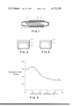
- FIG. 1 illustrates the apparatus for forming the amorphous phosphorus-nitrogen-oxygen material of the present invention.
- the apparatus includes a fused quartz (silicon dioxide) reactor tube 10. Surrounding the reactor wall is an induction heating coil 12 for heating the reactor and anything therein. Within the reactor is a graphite susceptor 14 which is enclosed in a fused quartz (silicon dioxide) envelope 16. Substrates 18 such as silicon semiconductor wafers are positioned over the graphite susceptor. The temperature of the substrates 18 are raised by RF induction heating process until the substrate temperature is between about 400°-900° C.
- reaction gases containing phosphorus, nitrogen and oxygen source are then passed through the chamber where the deposition of the amorphous phosphorus-nitrogen-oxygen material occurs onto the substrates 18.
- the preferred gases are phosphine (PH 3 ), ammonia (NH 3 ) and oxygen (O 2 ) with nitrogen carrier gas.
- FIGS. 2 and 3 Examples of the resulting structures are shown in FIGS. 2 and 3.
- FIG. 2 illustrates a silicon wafer 20 having a silicon dioxide coating 22 thereon and a phosphorus nitrogen oxygen coating of the present invention 24 over the silicon dioxide coating 22.
- FIG. 3 illustrates a silicon substrate 20 having the phosphorus nitrogen oxygen coating 24 of the present invention directly on the silicon substrate.
- Semiconductor devices may be formed within the silicon substrate 20 and the coating 24 can act either as a passivating coating or a masking coating for diffusion or ion implantation steps.
- oxygen in the resulting phosphorus nitrogen product is critical so that the coating will adhere properly to substrates and will be stable and not be decomposed as would oxygen free coatings of phosphorus nitride at ordinary temperatures.
- Oxygen is preferably brought into the compound by the addition of oxygen gas to the reaction gases. The addition of oxygen also rapidly promotes the deposition rate.
- FIG. 4 illustrates the formation region of the phosphorus nitrogen oxygen amorphous composition over the deposition temperature range of about 400°-900° C.
- the oxygen concentration in the feed gaseous mixture is from 0.01 to about 98% excluding the ammonia and phosphine.
- the crosses indicate data points where good adhering and stable coatings were formed.
- the squares indicate points of no deposition of the material of the present invention.
- the preferred gaseous materials for deposition of the coating of phosphorus-nitrogen-oxygen is ammonia, phosphine and oxygen. This is because such gases are available in high purity and in simple molecular form. Consequently, undesirable side reactions can be minimized. Furthermore, source materials in gaseous state provide the great easiness for CVD process control.
- P, P 2 O 5 and NH 4 Cl gases which could be used in place of phosphine, ammonia and oxygen are P, P 2 O 5 , NH 4 Cl, N 2 O, NO, etc.
- P, P 2 O 5 and NH 4 Cl are used, they have to be preheated to suitable temperature, and their vapor can be swept into the reaction chamber by inert carrier gas.
- Suitable carrier gases in addition to nitrogen are He, Ar, and other inert gases or mixtures thereof.
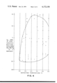
- FIG. 5 there is shown the deposition rate in Angstroms/minute versus the deposition temperature for the chemical vapor deposition using phosphine, ammonia, oxygen and nitrogen carrier gas at a given feed rate of phosphine, 2.12 cc/min. It is seen that the deposition rate peaks at about 500° C. deposition temperature. The deposition rate then drops down to the level of somewhat less than 200 Angstroms/min. around 800° C. This deposition rate with respect to deposition temperature can be higher or lower depending on the feed rates of source materials, particularly the phosphine concentration.
- the chemical vapor deposited (CVD) phosphorus-nitrogen-oxygen film is a coherent, homogeneous, amorphous material.
- the processes take place in the deposition. These include, simultaneously, chemical reactions, mass and energy transfers.
- the overall reaction is as follows:
- (P x N y O z ) n is CVD formed dense material, free of any crystallinity.
- P 2 O 5 and H 2 O appear to be the essential reaction by-products along with unidentified trace products in the existing gaseous stream.
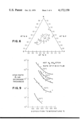
- Microprobe analysis of the film (5000 to 7000 A thickness) with chemical formula shown above, (P x N y O z ) n indicates X value varying from 30 to 32 atomic percent, y value from 36 to 48 atomic percent and z value from 21 to 33 atomic percent depending on the oxygen concentration in the feed gases mixture as well as deposition temperature.
- Wt.% ranges may vary somewhat when deposition temperatures are above or below 650° C.
- FIG. 8 illustrates the preferred composition region of (P x N y O z ) n at 650° C.
- FIG. 8 gives O, N and P in atomic percent.
- the TABLE I gives for Points 4-10 the deposition conditions and O, N and P in the resultant film in weight percent.
- Points 1 and 2 represent the compounds PN and P 3 N 5 , respectively, and Point 3 the simple PON compound. All of these known compounds are prepared by methods other than the CVD process.
- Points 8 and 9 of FIG. 6 represent boron doped (P x N y O z ) n films at 650° C. and 800° C. Compositions of the doped films shown in this P-N-O diagram are arrived at by neglecting the boron content because the light boron element is beyond the test probe detection capability.
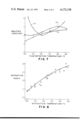
- the dielectric constant of the phosphorus-nitrogen-oxygen film varies from 8 to about 6 depending upon the film deposition temperature as shown from this graph.
- the highest dielectric constant is obtainable at the lower film deposition temperatures.
- the dielectric constant does increase at the higher deposition temperatures of the order of 800°-900° C. wherein it approaches the higher dielectric constant obtained at the low approximately 400° C. film deposition.
- the minimum film dielectric constant of the material is obtained in the order of 600° C.
- the graph compares the present material, curve 30, to silicon nitride as deposited 32 and silicon nitride after a 20 hour 1000° C. nitrogen annealing 34.
- Prolonged annealing of Si 3 N 4 generally increases the dielectric constant due to an extensive increase of crystallinity of silicon nitride. With the exception of the present material deposited at temperatures below 550° C., this truly amorphous material has comparable dielectric constant to silicon nitride with or without post-deposition anneal.
- the refractive index is also dependent upon the deposition temperature as shown by FIG. 8.
- the data points on this graph show experimental points where coatings of the phosphorus-nitrogen-oxygen material were deposited at the various deposition temperatures using the CVD chemical vapor deposition process of phosphine, ammonia, and nitrogen carrier gas.
- the results show that a steady increase in the refractive index is obtained when moving from the 400° C. deposition temperature to the 900° C. deposition temperature in the refractive index from about 1.6 to 2.0 as determined at wavelength 5461 A.
- the dielectric constant of the present material is also dependent on oxygen concentration as well as the deposition temperature. TABLE II illustrates examples of such property dependence.
- the TABLE III indicates the dielectric breakdown strength (accumulation mode) for the phosphorus-nitrogen-oxygen coatings deposited on the bare silicon substrates using phosphine, ammonia, oxygen and nitrogen carrier gas.
- the dielectric breakdown strength of TABLE III was measured by the ramp method on 20 mil diameter aluminum dot over the P-N-O film of approximately 1000 A on N type (100) Si substrates. For comparison purpose, all the breakdown strength was calculated based on equivalent silicon dioxide thickness. As compared to Si 3 N 4 films deposited on Si substrates in the same temperature range, the breakdown strength of P-N-O film is two to three times better than that of silicon nitride. In comparison with Si 3 N 4 , P-N-O coating not only shows higher dielectric breakdown strength, but also exhibits better compatibility to silicon substrate. Films of the P-N-O coating up to 2 microns in thickness on silicon do not cause any stress cracking or substrate warpage. Si 3 N 4 on silicon substrate generally shows cracks and warpage when its thickness reaches 0.8 microns.
- the phosphorus-nitrogen-oxygen material is very stable and does not decompose at normal temperatures in the range of 900° C.
- the material is not attacked by water, sulphuric acid, hydrochloric acid, hydrofluoric acid, phosphoric acid, ammonium hydroxide, hydrogen peroxide, ammonium hydroxide plus hydrogen peroxide, hydrogen peroxide plus hydrochloric acid, nitric acid, hydrofluoric acid plus nitric acid, aqua regia, sodium hydroxide solution (about 50%), pyrocatechol-ethylemediamine-water system. It is not even wetted by hydrofluoric acid solution.
- Reactive ion etching may be satisfactorily accomplished using a carbon tetrachloride system. For example, in carbon tetrachloride reactive ion etching at a temperature of 225° C. will etch the phosphorus-nitrogen-oxygen material at about 30 Angstroms per second.
- the P-N-O material is virtually not attacked by concentrated sulfuric acid (H 2 SO 4 ) at temperatures below 100° C.
- the material can be chemically etched only with concentrated H 2 SO 4 at elevated temperatures.
- FIG. 9 shows the etch rate of the material using 96% H 2 SO 4 at temperatures from 100° C. to 230° C.
- the P-N-O film is CVD coated with approximately 1000 A SiO 2 , then processed with conventional photolithography etching off unwanted oxide area.
- High temperature concentrated H 2 SO 4 etch will remove the P-N-O film through the opened oxide window.
- the preferred etching temperature using H 2 SO 4 is above about 190° C. and below the boiling or fuming point of H 2 SO 4 .
- this phosphorus-nitrogen-oxygen amorphous material because of its excellent stability and ability to withstand chemical attack.
- One important application would be as a diffusion source for phosphorus into silicon wafers. This diffusion would produce an N type region in silicon which is important in the manufacture of transistors and integrated circuits.
- High levels of phosphorus concentration in the diffused region can be produced from the present coating of in the order of 10 20 to 10 21 atoms per cc. and the junction depth of 1.2 to 1.4 microns. Diffusion was carried out at 1000° C. or higher in O 2 ambient.
- P-N-O film deposited on Si wafers of 0.5 to 1 microns in thickness was positioned in about 0.030" away from the device to be diffused. The time at temp. is about 1/2 to 1 hour with O 2 at 1 liter/min. flowing through the reaction tube.
- P-N-O film in FET memory devices in the gate region.
- the structure would be, for example:
- MFS Metal/P-N-O film/silicon device
- MPOS Metal/P-N-O film/SiO 2 silicon device
- Silicon substrates were placed on the graphite susceptor of the horizontal reactor shown in FIG. 1.
- the reactor was 31/4" by 21/4" and 30" long.
- the induction heating was turned on and the temperature of the silicon substrates was raised to between 400° and 900° C. depending upon the particular experiment within this example.
- Constant gaseous feed rates of phosphine PH 3 was 2.1 cc/min. and ammonia NH 3 was 200 cc/min.
- the oxygen content in the nitrogen carrier gas was varied.
- the oxygen was varying from 1 to 5000 cc/min. and N 2 from 0.1 liters/min. to 20.5 liters/min. depending on the deposition temperature. In FIG. 4, the lowest amount of O 2 in the feed is one cc/min.
- the maximum N 2 in the feed mixture is 20.5 liters/min.
- the total flow rate generally increases with deposition temperature.
- Films in FIG. 4 have thickness varying from approximately 1000 A to a few microns.
- the crosses and squares on FIG. 4 are actual data points of deposition temperature in °C. versus oxygen concentration in feed gaseous mixture excluding ammonia and phosphine. It is seen from the FIG. 4 that the phosphorus-nitrogen-oxygen material is only successfully formed within the dashed line. Outside of this dashed line either no deposition occurred or unstable coating occured.
- a silicon wafer having a phosphorous-nitrogen-oxygen coating thereon was subjected to boiling water at the deposition temperatures of 470°, 500° and 700° C.
- the coating was not affected after 7 days of continuous subjection to boiling water.
- Phosphorus-nitrogen-oxygen coating at temperatures above 450° C. was not affected after 12 days of continuous subjection to room temperature water.
- Silicon wafers having phosphorous-nitrogen-oxygen coatings thereon were formed at the film deposition temperatures specified in the TABLE V.
- the wafers were subjected to a temperature of 1000° C. in O 2 for one hour. The coatings disappeared.
- the wafers were then cleaned with HF and rinsed in H 2 O.
- the diffusion results showed a shallow junction of 0.18 to 0.29 microns, surface concentration in the order of 10 19 atoms/cm 3 and sheet resistance from 300 to 1000 ohm/square.
- the data showed no dependence of film deposition temperature.
Abstract
A method is described which forms amorphous phosphorus-nitrogen-oxygen material having excellent thermal stability and low reactivity to a wide variety of chemicals. The material is manufactured using a chemical vapor deposition process. The reaction chamber is maintained at a temperature between about 400°-900° C. with a suitable substrate placed therein. Reaction gases containing phosphorus-nitrogen-bearing compounds and a source of oxygen are passed through the chamber to deposit the phosphorus-nitrogen-oxygen film onto the substrate.
Description
The invention relates to a new composition of matter which is an amorphous-phosphorus-nitrogen-oxygen material which has excellent physical characteristics and a method for manufacturing the material as well as applications.
Phosphorus and nitrogen compositions have been known and are described, for example, in the C. G. Miner U.S. Pat. No. 1,634,795, C. G. Christian U.S. Pat. No. 2,884,318, H. Ulrich U.S. Pat. No. 3,859,418 and M. Yamashita et al U.S. Pat. No. 3,931,039. The principal use of these nitride materials have been in fertilizers or plant foods. Another proposed use was as a diffusing source for phosphorus into silicon wafers to produce N-type regions in the production of semiconductor devices such as transistors and integrated circuits. It has been in this context that the Yamashita et al U.S. Pat. No. 3,931,039 describes in its prior art a method for forming a phosphorus nitride coating in column 1 of the patent. It is pointed out in this patent that the phosphorus nitride coating is thermally unstable and readily decomposes. The patent goes on to describe a method for forming a thermally stable phosphorus nitride-silicon dioxide composition which is usable as a diffusion source of N-type impurities for the formation of semiconductor devices.
In accordance with the present invention, an amorphous phosphorus-nitrogen-oxygen coating is described which is thermally stable and unattacked by a wide variety of normally very reactive chemicals. The coating composition is manufactured by chemically reacting vapor phosphorus and nitrogen compounds to form a phosphorus nitrogen coating at temperatures between about 400°-900° C. An excellent physical property coating is formed by the addition of a gaseous oxygen source in the reaction gases to bring a oxygen component to the phosphorus nitrogen composition.
FIG. 1 illustrates one form of reaction chamber for manufacturing the composition of the present invention;
FIGS. 2 and 3 illustrate structures in using the composition of the present invention in electronic semiconductor structures;
FIG. 4 is a graphical representation of the formation region of the composition as it is dependent upon the oxygen source concentration in the feed gaseous mixture versus the deposition temperature;
FIG. 5 illustrates the effect of deposition temperature upon deposition rate;
FIG. 6 shows compositions of P-N-O and boron doped P-N-O coatings fabricated at 650° C.
FIG. 7 compares the dielectric constant versus deposition temperature of the composition of the present invention with that of silicon nitride;
FIG. 8 shows the relationship between the deposition temperature of the material of the present invention versus the refractive index of the resulting coating; and
FIG. 9 illustrates the etch rate of coatings with H2 SO4 at temperatures from 100° C. to 230° C.
FIG. 1 illustrates the apparatus for forming the amorphous phosphorus-nitrogen-oxygen material of the present invention. The apparatus includes a fused quartz (silicon dioxide) reactor tube 10. Surrounding the reactor wall is an induction heating coil 12 for heating the reactor and anything therein. Within the reactor is a graphite susceptor 14 which is enclosed in a fused quartz (silicon dioxide) envelope 16. Substrates 18 such as silicon semiconductor wafers are positioned over the graphite susceptor. The temperature of the substrates 18 are raised by RF induction heating process until the substrate temperature is between about 400°-900° C. The reaction gases containing phosphorus, nitrogen and oxygen source are then passed through the chamber where the deposition of the amorphous phosphorus-nitrogen-oxygen material occurs onto the substrates 18. The preferred gases are phosphine (PH3), ammonia (NH3) and oxygen (O2) with nitrogen carrier gas.
Examples of the resulting structures are shown in FIGS. 2 and 3. FIG. 2 illustrates a silicon wafer 20 having a silicon dioxide coating 22 thereon and a phosphorus nitrogen oxygen coating of the present invention 24 over the silicon dioxide coating 22. FIG. 3 illustrates a silicon substrate 20 having the phosphorus nitrogen oxygen coating 24 of the present invention directly on the silicon substrate. Semiconductor devices may be formed within the silicon substrate 20 and the coating 24 can act either as a passivating coating or a masking coating for diffusion or ion implantation steps.
The presence of oxygen in the resulting phosphorus nitrogen product is critical so that the coating will adhere properly to substrates and will be stable and not be decomposed as would oxygen free coatings of phosphorus nitride at ordinary temperatures. Oxygen is preferably brought into the compound by the addition of oxygen gas to the reaction gases. The addition of oxygen also rapidly promotes the deposition rate.
FIG. 4 illustrates the formation region of the phosphorus nitrogen oxygen amorphous composition over the deposition temperature range of about 400°-900° C. The oxygen concentration in the feed gaseous mixture is from 0.01 to about 98% excluding the ammonia and phosphine. The crosses indicate data points where good adhering and stable coatings were formed. The squares indicate points of no deposition of the material of the present invention. The preferred gaseous materials for deposition of the coating of phosphorus-nitrogen-oxygen is ammonia, phosphine and oxygen. This is because such gases are available in high purity and in simple molecular form. Consequently, undesirable side reactions can be minimized. Furthermore, source materials in gaseous state provide the great easiness for CVD process control. Other gaseous materials which could be used in place of phosphine, ammonia and oxygen are P, P2 O5, NH4 Cl, N2 O, NO, etc. When P, P2 O5 and NH4 Cl are used, they have to be preheated to suitable temperature, and their vapor can be swept into the reaction chamber by inert carrier gas. Suitable carrier gases in addition to nitrogen are He, Ar, and other inert gases or mixtures thereof.
Referring to FIG. 5, there is shown the deposition rate in Angstroms/minute versus the deposition temperature for the chemical vapor deposition using phosphine, ammonia, oxygen and nitrogen carrier gas at a given feed rate of phosphine, 2.12 cc/min. It is seen that the deposition rate peaks at about 500° C. deposition temperature. The deposition rate then drops down to the level of somewhat less than 200 Angstroms/min. around 800° C. This deposition rate with respect to deposition temperature can be higher or lower depending on the feed rates of source materials, particularly the phosphine concentration.
The chemical vapor deposited (CVD) phosphorus-nitrogen-oxygen film is a coherent, homogeneous, amorphous material. The processes take place in the deposition. These include, simultaneously, chemical reactions, mass and energy transfers. The overall reaction is as follows:
N.sub.2 +PH.sub.3 +NH.sub.3 +O.sub.2 →(P.sub.x N.sub.y O.sub.z).sub.n +P.sub.2 O.sub.5 +H.sub.2 O+N.sub.2
in which (Px Ny Oz)n is CVD formed dense material, free of any crystallinity. P2 O5 and H2 O appear to be the essential reaction by-products along with unidentified trace products in the existing gaseous stream. Microprobe analysis of the film (5000 to 7000 A thickness) with chemical formula shown above, (Px Ny Oz)n, indicates X value varying from 30 to 32 atomic percent, y value from 36 to 48 atomic percent and z value from 21 to 33 atomic percent depending on the oxygen concentration in the feed gases mixture as well as deposition temperature.
Preferred composition in terms of wt.% of P--N--O film in the formula (Px Ny Oz)n is:
P--48-50 Wt.%
N--29-36 Wt.%
O--10-27 Wt.%
These Wt.% ranges may vary somewhat when deposition temperatures are above or below 650° C.
FIG. 8 illustrates the preferred composition region of (Px Ny Oz)n at 650° C. FIG. 8 gives O, N and P in atomic percent. The TABLE I gives for Points 4-10 the deposition conditions and O, N and P in the resultant film in weight percent.
              TABLE I
______________________________________
           O.sub.2 % in Gas-
           eous Feed
                    Wt. % -
Point #
       Temp. ° C.
                 Mixture    O     N     P
______________________________________
4      650        0.015     16.24±
                                  33.86±
                                        49.89±
                            0.49  0.37  0.30
5      650        0.35      20.93±
                                  30.52±
                                        48.54±
                            1.92  0.76  1.28
6      650       24         21.32±
                                  29.58±
                                        49.09±
                            0.75  0.54  0.79
7      650       47.6       21.51±
                                  29.71±
                                        48.76±
                            1.77  1.24  0.72
8      650       91         26.44±
                                  25.77±
                                        47.78±
                            0.57  0.41  0.77
9      650        0.35(100  10.06±
                                  35.50±
                                        50.42±
                 cc/min.)   1.48  0.51  1.19
                 (B.sub.2 H.sub.6)
10     800       24 (300    16.57±
                                  35.74±
                                        47.67±
                 cc/min.    0.94  0.60  0.63
                 (B.sub.2 H.sub.6)
______________________________________
Points 1 and 2 represent the compounds PN and P3 N5, respectively, and Point 3 the simple PON compound. All of these known compounds are prepared by methods other than the CVD process. Points 8 and 9 of FIG. 6 represent boron doped (Px Ny Oz)n films at 650° C. and 800° C. Compositions of the doped films shown in this P-N-O diagram are arrived at by neglecting the boron content because the light boron element is beyond the test probe detection capability. The (Px Ny Oz)n film when deposited on a thick silicon wafer with thickness of about 1 micron, exhibits three broad, strong characteristic absorption bands centered at 1230, 910 and 480 cm-1. These bands show very feeble shift with variation of oxygen concentration during deposition.
Referring now to FIG. 7, the dielectric constant of the phosphorus-nitrogen-oxygen film varies from 8 to about 6 depending upon the film deposition temperature as shown from this graph. The highest dielectric constant is obtainable at the lower film deposition temperatures. However, the dielectric constant does increase at the higher deposition temperatures of the order of 800°-900° C. wherein it approaches the higher dielectric constant obtained at the low approximately 400° C. film deposition. The minimum film dielectric constant of the material is obtained in the order of 600° C. The graph compares the present material, curve 30, to silicon nitride as deposited 32 and silicon nitride after a 20 hour 1000° C. nitrogen annealing 34. Prolonged annealing of Si3 N4 generally increases the dielectric constant due to an extensive increase of crystallinity of silicon nitride. With the exception of the present material deposited at temperatures below 550° C., this truly amorphous material has comparable dielectric constant to silicon nitride with or without post-deposition anneal.
The refractive index is also dependent upon the deposition temperature as shown by FIG. 8. The data points on this graph show experimental points where coatings of the phosphorus-nitrogen-oxygen material were deposited at the various deposition temperatures using the CVD chemical vapor deposition process of phosphine, ammonia, and nitrogen carrier gas. The results show that a steady increase in the refractive index is obtained when moving from the 400° C. deposition temperature to the 900° C. deposition temperature in the refractive index from about 1.6 to 2.0 as determined at wavelength 5461 A.
The dielectric constant of the present material is also dependent on oxygen concentration as well as the deposition temperature. TABLE II illustrates examples of such property dependence.
              TABLE II
______________________________________
       Refrac-
       tive    Film                        Dielec-
Deposi-
       Index   Thick-                      tric
tion   n at    ness    O.sub.2
                             N.sub.2 liter
                                    O.sub.2 %
                                           Con-
Temp. ° C.
       5461A   in A    cc/min
                             per min.
                                    in Feed
                                           stant
______________________________________
860    1.89    1046    5000  15.5   24.4   6.95
800    1.942    960    10    20.5   0.05   7.49
800    1.931    813    8     20.5   0.039  6.8
550    1.711   1130    4     10.5   0.038  6.3
550    1.722   1151    2     10.5   0.019  6.3
500    1.717   1169    2     8.8    0.0235 6.2
450    1.682   1189    2     7.5    0.0266 6.74
655    1.876   1000    2     12.5   0.016  6.8
850    1.961    882    8     20.5   0.039  7.08
610    1.772    863    2     12.5   0.016  6.58
800    1.857   1229    5000  15.5   24.4   6.54
650    1.747   1299    5000  5.5    47.6   6.7
700    1.931    922.7  2     16.5   0.012  6.75
______________________________________
The TABLE III indicates the dielectric breakdown strength (accumulation mode) for the phosphorus-nitrogen-oxygen coatings deposited on the bare silicon substrates using phosphine, ammonia, oxygen and nitrogen carrier gas.
              TABLE III
______________________________________
Deposition Temp. ° C.
               Breakdown Strength, × 10.sup.6 V /cm
______________________________________
500            13.8
600            14.7
700            12.8
800            84
860            10
______________________________________
The dielectric breakdown strength of TABLE III was measured by the ramp method on 20 mil diameter aluminum dot over the P-N-O film of approximately 1000 A on N type (100) Si substrates. For comparison purpose, all the breakdown strength was calculated based on equivalent silicon dioxide thickness. As compared to Si3 N4 films deposited on Si substrates in the same temperature range, the breakdown strength of P-N-O film is two to three times better than that of silicon nitride. In comparison with Si3 N4, P-N-O coating not only shows higher dielectric breakdown strength, but also exhibits better compatibility to silicon substrate. Films of the P-N-O coating up to 2 microns in thickness on silicon do not cause any stress cracking or substrate warpage. Si3 N4 on silicon substrate generally shows cracks and warpage when its thickness reaches 0.8 microns.
The phosphorus-nitrogen-oxygen material is very stable and does not decompose at normal temperatures in the range of 900° C. The material is not attacked by water, sulphuric acid, hydrochloric acid, hydrofluoric acid, phosphoric acid, ammonium hydroxide, hydrogen peroxide, ammonium hydroxide plus hydrogen peroxide, hydrogen peroxide plus hydrochloric acid, nitric acid, hydrofluoric acid plus nitric acid, aqua regia, sodium hydroxide solution (about 50%), pyrocatechol-ethylemediamine-water system. It is not even wetted by hydrofluoric acid solution.
The stability of the material is such it is difficult to etch using normal chemical etching techniques. Reactive ion etching may be satisfactorily accomplished using a carbon tetrachloride system. For example, in carbon tetrachloride reactive ion etching at a temperature of 225° C. will etch the phosphorus-nitrogen-oxygen material at about 30 Angstroms per second.
The P-N-O material is virtually not attacked by concentrated sulfuric acid (H2 SO4) at temperatures below 100° C. The material, however, can be chemically etched only with concentrated H2 SO4 at elevated temperatures. FIG. 9 shows the etch rate of the material using 96% H2 SO4 at temperatures from 100° C. to 230° C. For pattern definition, the P-N-O film is CVD coated with approximately 1000 A SiO2, then processed with conventional photolithography etching off unwanted oxide area. High temperature concentrated H2 SO4 etch will remove the P-N-O film through the opened oxide window. The preferred etching temperature using H2 SO4 is above about 190° C. and below the boiling or fuming point of H2 SO4.
There are many applications where this phosphorus-nitrogen-oxygen amorphous material because of its excellent stability and ability to withstand chemical attack. One important application would be as a diffusion source for phosphorus into silicon wafers. This diffusion would produce an N type region in silicon which is important in the manufacture of transistors and integrated circuits. High levels of phosphorus concentration in the diffused region can be produced from the present coating of in the order of 1020 to 1021 atoms per cc. and the junction depth of 1.2 to 1.4 microns. Diffusion was carried out at 1000° C. or higher in O2 ambient. P-N-O film deposited on Si wafers of 0.5 to 1 microns in thickness was positioned in about 0.030" away from the device to be diffused. The time at temp. is about 1/2 to 1 hour with O2 at 1 liter/min. flowing through the reaction tube.
Another important application is the use of the P-N-O film in FET memory devices in the gate region. The structure would be, for example:
(1) Metal/P-N-O film/silicon device (MPS).
(2) Metal/P-N-O film/SiO2 silicon device (MPOS).
(3) Silicon/P-N-O film/SiO2 /silicon device (SPOS).
TABLE IV gives experimental data on MPOS [Al metal(Px Ny Oz)n -SiO2 -Si] device where a 20 mil diameter Al dot on (Px Ny Oz)n over 200 A SiO2 on P(100) Si substrate.
              TABLE IV
______________________________________
                  Equivalent        Net Charge
Temp. ° C.
         O.sub.2 %
                  Oxide A   V.sub.FB
                                    per cm.sup.2
______________________________________
800      0.034    289       -1.20V  2.87 × 10.sup.11
850      0.034    268       -1.10V  2.32 × 10.sup.11
700      0.014    291       -1.20V  2.85 × 10.sup.11
600      0.016    323       -1.12V  2.06 × 10.sup.11
500      0.024    320       -0.99V  1.23 × 10.sup.11
450      0.026    310       -0.96V  1.07 × 10.sup.11
______________________________________
Other applications include wire insulation, capacitor, protective coating for integrated circuits or other uses, such as etching mask.
The following examples are included merely to aid in the understanding of the invention and variations may be made by one skilled in the art without departing from the spirit and scope of the invention.
Silicon substrates were placed on the graphite susceptor of the horizontal reactor shown in FIG. 1. The reactor was 31/4" by 21/4" and 30" long. The induction heating was turned on and the temperature of the silicon substrates was raised to between 400° and 900° C. depending upon the particular experiment within this example. Constant gaseous feed rates of phosphine PH3 was 2.1 cc/min. and ammonia NH3 was 200 cc/min. The oxygen content in the nitrogen carrier gas was varied. The oxygen was varying from 1 to 5000 cc/min. and N2 from 0.1 liters/min. to 20.5 liters/min. depending on the deposition temperature. In FIG. 4, the lowest amount of O2 in the feed is one cc/min. and the highest 5000 cc/min. The maximum N2 in the feed mixture is 20.5 liters/min. At each deposition temperature there is a favorable total feed rate so that the most uniform film thickness can be produced. The total flow rate generally increases with deposition temperature. Films in FIG. 4 have thickness varying from approximately 1000 A to a few microns. The crosses and squares on FIG. 4 are actual data points of deposition temperature in °C. versus oxygen concentration in feed gaseous mixture excluding ammonia and phosphine. It is seen from the FIG. 4 that the phosphorus-nitrogen-oxygen material is only successfully formed within the dashed line. Outside of this dashed line either no deposition occurred or unstable coating occured.
A silicon wafer having a phosphorous-nitrogen-oxygen coating thereon was subjected to boiling water at the deposition temperatures of 470°, 500° and 700° C. The coating was not affected after 7 days of continuous subjection to boiling water.
Phosphorus-nitrogen-oxygen coating at temperatures above 450° C. was not affected after 12 days of continuous subjection to room temperature water.
Silicon wafers having phosphorous-nitrogen-oxygen coatings thereon were formed at the film deposition temperatures specified in the TABLE V. The wafers were subjected to a temperature of 1000° C. in O2 for one hour. The coatings disappeared. The wafers were then cleaned with HF and rinsed in H2 O. The diffusion results showed a shallow junction of 0.18 to 0.29 microns, surface concentration in the order of 1019 atoms/cm3 and sheet resistance from 300 to 1000 ohm/square. The data showed no dependence of film deposition temperature.
              TABLE V
______________________________________
Film                   Surface     Sheet
Deposition
          Junction     Concentration
                                   Resistance
Temp. ° C.
          Depth,Microns
                       in atoms/cm.sup.3
                                   ohm/square
______________________________________
4A  400       0.29         10.sup.19.2
                                     240
4B  450       0.19         10.sup.18.7
                                     1003
4C  650       0.18         10.sup.18.5
                                     951
4D  750       0.21         10.sup.19.2
                                     418
4E  900       0.25         10.sup.19.2
                                     309
______________________________________
While the invention has been particularly shown and described with reference to preferred embodiments thereof, it will be understood by those skilled in the art that the foregoing and other changes in form and details may be made without departing from the spirit and scope of the invention.
Claims (10)
1. A method for forming phosphorus-nitrogen-oxygen film comprising:
providing a reaction chamber having a substrate temperature of about 400° to 900° C. with a suitable substrate; and
passing the reaction gases PH3, NH3 and a gas which is a source of oxygen through the chamber to deposit said phosphorus-nitrogen-oxygen film onto said substrate.
2. The method of claim 1 wherein the said gas which is a source of oxygen is O2.
3. The method of claim 1 wherein the reaction chamber has a substrate temperature of about 450° to 850° C.
4. The method of claim 2 wherein the said O2 gas is greater than about 0.01% of the reaction gas mixture.
5. The method of claim 1 wherein gas feed rates are between about 0.5 and 2.5 cc/min. for PH3 and between about 100 cc/min. and 300 cc/min. for NH3.
6. The method of claim 5 wherein the said gas which is a source of oxygen is O2 and its content in O2 -inert gas portion of the feed gases between about 0.01% to 98%.
7. The method of claim 1 wherein an inert carrier gas is used and its feed rate is between about 3 liters/min. and 20.5 liters/min.
8. The method of claim 7 wherein the said inert carrier gas is N2.
9. The method of claim 1 wherein a source of boron is included in the reaction gases to dope the said deposit with boron.
10. The method of claim 9 wherein the source of boron is B2 H6 gas.
Priority Applications (16)
| Application Number | Priority Date | Filing Date | Title |
|---|---|---|---|
| US05/772,804 US4172158A (en) | 1977-02-28 | 1977-02-28 | Method of forming a phosphorus-nitrogen-oxygen film on a substrate |
| AU32529/78A AU515993B2 (en) | 1977-02-28 | 1978-01-18 | Preparation and applications of phosphorus nitrogen oxygen compositions |
| FR7802445A FR2381563A1 (en) | 1977-02-28 | 1978-01-20 | FORMULATION COMPOUND (PXNYOZ) N, METHOD OF MANUFACTURING A FILM FROM THE SAID COMPOUND, AND APPLICATION OF THE SAID COMPOUND TO INTEGRATED CIRCUIT TECHNOLOGY |
| JP628478A JPS53107273A (en) | 1977-02-28 | 1978-01-25 | Film composition of phosphorus* nitrogen and oxygen amorphous material |
| BE184699A BE863405A (en) | 1977-02-28 | 1978-01-27 | FORMULATION COMPOUND (PXNYOZ) N, METHOD OF MANUFACTURING A FILM FROM THE SAID COMPOUND, AND ITS APPLICATION TO INTEGRATED CIRCUITS |
| GB3626/78A GB1592022A (en) | 1977-02-28 | 1978-01-30 | Phosphorus-nitrogen-oxygen film and method for making such film |
| IT20141/78A IT1110455B (en) | 1977-02-28 | 1978-02-10 | PROCESS FOR THE MANUFACTURE OF PHOSPHORUS NITROGEN COMPOUNDS |
| ES466902A ES466902A1 (en) | 1977-02-28 | 1978-02-11 | Method of forming a phosphorus-nitrogen-oxygen film on a substrate |
| NL7802009A NL7802009A (en) | 1977-02-28 | 1978-02-22 | CHEMICAL VAPOR DEPOSITION OF A LAYER OF AMORPH PHOSPHORUS-NITROGEN-OXYGEN COMPOSITION, ETCHING OF SUCH LAYER, MATERIAL OF SUCH COMPOSITION AND SEMICONDUCTOR PROVIDED WITH SUCH LAYER. |
| DE19782807475 DE2807475A1 (en) | 1977-02-28 | 1978-02-22 | MATERIAL CONTAINING PHOSPHORUS AND NITROGEN, ITS PRODUCTION AND USE |
| BR7801098A BR7801098A (en) | 1977-02-28 | 1978-02-23 | PHOSPHORUS-NITROGEN-OXYGEN COMPOSITION, METHOD FOR THE MANUFACTURE OF SUCH COMPOSITION AND APPLICATIONS OF THE SAME |
| CA297,675A CA1096136A (en) | 1977-02-28 | 1978-02-24 | Phosphorus-nitrogen-oxygen composition and method for making such composition and applications of the same |
| SE7802183A SE427399B (en) | 1977-02-28 | 1978-02-27 | COATING COMPOSITION PREFERRED INTENDED FOR SEMICONDUCTORS AS WELL AS PREPARING THE COMPOSITION |
| US06/042,400 US4275409A (en) | 1977-02-28 | 1979-05-25 | Phosphorus-nitrogen-oxygen composition and method for making such composition and applications of the same |
| US06/042,642 US4289539A (en) | 1977-02-28 | 1979-05-25 | Phosphorus-nitrogen-oxygen composition and method for making such composition and applications of the same |
| US06/042,488 US4243475A (en) | 1977-02-28 | 1979-05-25 | Method for etching a phosphorus-nitrogen-oxygen coating |
Applications Claiming Priority (1)
| Application Number | Priority Date | Filing Date | Title |
|---|---|---|---|
| US05/772,804 US4172158A (en) | 1977-02-28 | 1977-02-28 | Method of forming a phosphorus-nitrogen-oxygen film on a substrate |
Related Child Applications (3)
| Application Number | Title | Priority Date | Filing Date |
|---|---|---|---|
| US06/042,488 Division US4243475A (en) | 1977-02-28 | 1979-05-25 | Method for etching a phosphorus-nitrogen-oxygen coating |
| US06/042,642 Division US4289539A (en) | 1977-02-28 | 1979-05-25 | Phosphorus-nitrogen-oxygen composition and method for making such composition and applications of the same |
| US06/042,400 Division US4275409A (en) | 1977-02-28 | 1979-05-25 | Phosphorus-nitrogen-oxygen composition and method for making such composition and applications of the same |
Publications (1)
| Publication Number | Publication Date |
|---|---|
| US4172158A true US4172158A (en) | 1979-10-23 |
Family
ID=25096283
Family Applications (1)
| Application Number | Title | Priority Date | Filing Date |
|---|---|---|---|
| US05/772,804 Expired - Lifetime US4172158A (en) | 1977-02-28 | 1977-02-28 | Method of forming a phosphorus-nitrogen-oxygen film on a substrate |
Country Status (13)
| Country | Link |
|---|---|
| US (1) | US4172158A (en) |
| JP (1) | JPS53107273A (en) |
| AU (1) | AU515993B2 (en) |
| BE (1) | BE863405A (en) |
| BR (1) | BR7801098A (en) |
| CA (1) | CA1096136A (en) |
| DE (1) | DE2807475A1 (en) |
| ES (1) | ES466902A1 (en) |
| FR (1) | FR2381563A1 (en) |
| GB (1) | GB1592022A (en) |
| IT (1) | IT1110455B (en) |
| NL (1) | NL7802009A (en) |
| SE (1) | SE427399B (en) |
Cited By (5)
| Publication number | Priority date | Publication date | Assignee | Title |
|---|---|---|---|---|
| US4275409A (en) * | 1977-02-28 | 1981-06-23 | International Business Machines Corporation | Phosphorus-nitrogen-oxygen composition and method for making such composition and applications of the same |
| US4485393A (en) * | 1978-05-16 | 1984-11-27 | Tokyo Shibaura Denki Kabushiki Kaisha | Semiconductor device with selective nitride layer over channel stop |
| US5070035A (en) * | 1988-01-25 | 1991-12-03 | Nippon Mining Co., Ltd. | Method for producing a iii-v compound semiconductor device with a phosphoric oxide insulating layer |
| DE4333160A1 (en) * | 1993-09-29 | 1995-03-30 | Siemens Ag | Production method for a nitrided silicon oxide layer with reduced thermal loading |
| US7148157B2 (en) | 2002-10-22 | 2006-12-12 | Chartered Semiconductor Manufacturing Ltd. | Use of phoslon (PNO) for borderless contact fabrication, etch stop/barrier layer for dual damascene fabrication and method of forming phoslon |
Citations (5)
| Publication number | Priority date | Publication date | Assignee | Title |
|---|---|---|---|---|
| US3486951A (en) * | 1967-06-16 | 1969-12-30 | Corning Glass Works | Method of manufacturing semiconductor devices |
| US3524776A (en) * | 1967-01-30 | 1970-08-18 | Corning Glass Works | Process for coating silicon wafers |
| US3660179A (en) * | 1970-08-17 | 1972-05-02 | Westinghouse Electric Corp | Gaseous diffusion technique |
| US3666574A (en) * | 1968-09-06 | 1972-05-30 | Westinghouse Electric Corp | Phosphorus diffusion technique |
| US3931039A (en) * | 1973-11-01 | 1976-01-06 | Denki Kagaku Kogyo Kabushiki Kaisha | Composition for diffusing phosphorus |
-
1977
- 1977-02-28 US US05/772,804 patent/US4172158A/en not_active Expired - Lifetime
-
1978
- 1978-01-18 AU AU32529/78A patent/AU515993B2/en not_active Expired
- 1978-01-20 FR FR7802445A patent/FR2381563A1/en active Granted
- 1978-01-25 JP JP628478A patent/JPS53107273A/en active Granted
- 1978-01-27 BE BE184699A patent/BE863405A/en not_active IP Right Cessation
- 1978-01-30 GB GB3626/78A patent/GB1592022A/en not_active Expired
- 1978-02-10 IT IT20141/78A patent/IT1110455B/en active
- 1978-02-11 ES ES466902A patent/ES466902A1/en not_active Expired
- 1978-02-22 DE DE19782807475 patent/DE2807475A1/en not_active Withdrawn
- 1978-02-22 NL NL7802009A patent/NL7802009A/en not_active Application Discontinuation
- 1978-02-23 BR BR7801098A patent/BR7801098A/en unknown
- 1978-02-24 CA CA297,675A patent/CA1096136A/en not_active Expired
- 1978-02-27 SE SE7802183A patent/SE427399B/en unknown
Patent Citations (5)
| Publication number | Priority date | Publication date | Assignee | Title |
|---|---|---|---|---|
| US3524776A (en) * | 1967-01-30 | 1970-08-18 | Corning Glass Works | Process for coating silicon wafers |
| US3486951A (en) * | 1967-06-16 | 1969-12-30 | Corning Glass Works | Method of manufacturing semiconductor devices |
| US3666574A (en) * | 1968-09-06 | 1972-05-30 | Westinghouse Electric Corp | Phosphorus diffusion technique |
| US3660179A (en) * | 1970-08-17 | 1972-05-02 | Westinghouse Electric Corp | Gaseous diffusion technique |
| US3931039A (en) * | 1973-11-01 | 1976-01-06 | Denki Kagaku Kogyo Kabushiki Kaisha | Composition for diffusing phosphorus |
Cited By (5)
| Publication number | Priority date | Publication date | Assignee | Title |
|---|---|---|---|---|
| US4275409A (en) * | 1977-02-28 | 1981-06-23 | International Business Machines Corporation | Phosphorus-nitrogen-oxygen composition and method for making such composition and applications of the same |
| US4485393A (en) * | 1978-05-16 | 1984-11-27 | Tokyo Shibaura Denki Kabushiki Kaisha | Semiconductor device with selective nitride layer over channel stop |
| US5070035A (en) * | 1988-01-25 | 1991-12-03 | Nippon Mining Co., Ltd. | Method for producing a iii-v compound semiconductor device with a phosphoric oxide insulating layer |
| DE4333160A1 (en) * | 1993-09-29 | 1995-03-30 | Siemens Ag | Production method for a nitrided silicon oxide layer with reduced thermal loading |
| US7148157B2 (en) | 2002-10-22 | 2006-12-12 | Chartered Semiconductor Manufacturing Ltd. | Use of phoslon (PNO) for borderless contact fabrication, etch stop/barrier layer for dual damascene fabrication and method of forming phoslon |
Also Published As
| Publication number | Publication date |
|---|---|
| FR2381563A1 (en) | 1978-09-22 |
| DE2807475A1 (en) | 1978-09-07 |
| JPS6155768B2 (en) | 1986-11-29 |
| GB1592022A (en) | 1981-07-01 |
| SE427399B (en) | 1983-03-28 |
| IT1110455B (en) | 1985-12-23 |
| AU3252978A (en) | 1979-07-26 |
| CA1096136A (en) | 1981-02-24 |
| BR7801098A (en) | 1978-11-28 |
| JPS53107273A (en) | 1978-09-19 |
| BE863405A (en) | 1978-05-16 |
| AU515993B2 (en) | 1981-05-14 |
| NL7802009A (en) | 1978-08-30 |
| ES466902A1 (en) | 1978-10-01 |
| IT7820141A0 (en) | 1978-02-10 |
| SE7802183L (en) | 1978-08-29 |
| FR2381563B1 (en) | 1982-05-14 |
Similar Documents
| Publication | Publication Date | Title |
|---|---|---|
| US3479237A (en) | Etch masks on semiconductor surfaces | |
| Eversteyn et al. | Influence of AsH3, PH 3, and B 2 H 6 on the Growth Rate and Resistivity of Polycrystalline Silicon Films Deposited from a SiH4‐H 2 Mixture | |
| US4349408A (en) | Method of depositing a refractory metal on a semiconductor substrate | |
| KR960011015B1 (en) | DEPOSITION OF SILICON DIOXIDE FILMS AT TEMPERATURE AS LOW AS 100í• BY LPCVD USING ORGANODISILANE SOURCES | |
| US3511703A (en) | Method for depositing mixed oxide films containing aluminum oxide | |
| EP0010910B1 (en) | Method for forming an insulating film layer on a semiconductor substrate surface | |
| Kooi | Formation and composition of surface layers and solubility limits of phosphorus during diffusion in silicon | |
| US4217375A (en) | Deposition of doped silicon oxide films | |
| JPH057872B2 (en) | ||
| JP3110857B2 (en) | Method for producing product including TiN x layer | |
| EP0470661B1 (en) | Method of providing a silicion dioxide layer on a substrate by means of chemical reaction from the vapour phase at a low pressure (LPCVD) | |
| JPH03120365A (en) | Sio2-adhering process | |
| Duffy et al. | Chemical vapor deposition of aluminum oxide films from organo-aluminum compounds | |
| US3558348A (en) | Dielectric films for semiconductor devices | |
| JPH05279838A (en) | Formation of silicon nitride film and semiconductor device | |
| US4172158A (en) | Method of forming a phosphorus-nitrogen-oxygen film on a substrate | |
| US3573096A (en) | Silane method for making silicon nitride | |
| Lee et al. | The preparation, characterization and application of plasma-enhanced chemically vapour deposited silicon nitride films deposited at low temperatures | |
| US4289539A (en) | Phosphorus-nitrogen-oxygen composition and method for making such composition and applications of the same | |
| Osenbach et al. | Behavior of a‐SiN: H and a‐SiON: H films in condensed water | |
| US5690737A (en) | Process for forming epitaxial BaF2 on GaAs | |
| US4243475A (en) | Method for etching a phosphorus-nitrogen-oxygen coating | |
| US4275409A (en) | Phosphorus-nitrogen-oxygen composition and method for making such composition and applications of the same | |
| Ahmed et al. | Borophosphosilicate glass crystal induction and suppression | |
| US4401691A (en) | Oxidation of silicon wafers to eliminate white ribbon |