US4242149A - Method of making photodetectors using ion implantation and laser annealing - Google Patents
Method of making photodetectors using ion implantation and laser annealing Download PDFInfo
- Publication number
- US4242149A US4242149A US06/062,593 US6259379A US4242149A US 4242149 A US4242149 A US 4242149A US 6259379 A US6259379 A US 6259379A US 4242149 A US4242149 A US 4242149A
- Authority
- US
- United States
- Prior art keywords
- substrate
- ions
- compound
- elements
- predetermined depth
- Prior art date
- Legal status (The legal status is an assumption and is not a legal conclusion. Google has not performed a legal analysis and makes no representation as to the accuracy of the status listed.)
- Expired - Lifetime
Links
- 238000004519 manufacturing process Methods 0.000 title claims 2
- 238000005468 ion implantation Methods 0.000 title description 3
- 238000005224 laser annealing Methods 0.000 title 1
- 239000000758 substrate Substances 0.000 claims abstract description 36
- 150000002500 ions Chemical class 0.000 claims abstract description 32
- 238000000034 method Methods 0.000 claims abstract description 20
- 150000001875 compounds Chemical class 0.000 claims abstract description 12
- 239000004065 semiconductor Substances 0.000 claims abstract description 6
- 238000010849 ion bombardment Methods 0.000 claims abstract description 3
- 238000004093 laser heating Methods 0.000 claims description 3
- 230000000737 periodic effect Effects 0.000 claims description 3
- 239000007943 implant Substances 0.000 claims description 2
- MARUHZGHZWCEQU-UHFFFAOYSA-N 5-phenyl-2h-tetrazole Chemical compound C1=CC=CC=C1C1=NNN=N1 MARUHZGHZWCEQU-UHFFFAOYSA-N 0.000 abstract description 10
- 238000001704 evaporation Methods 0.000 abstract description 4
- 230000008020 evaporation Effects 0.000 abstract description 3
- QSHDDOUJBYECFT-UHFFFAOYSA-N mercury Chemical compound [Hg] QSHDDOUJBYECFT-UHFFFAOYSA-N 0.000 abstract description 2
- 229910052753 mercury Inorganic materials 0.000 abstract description 2
- 238000000137 annealing Methods 0.000 description 7
- 229910000661 Mercury cadmium telluride Inorganic materials 0.000 description 5
- 229910001218 Gallium arsenide Inorganic materials 0.000 description 3
- 239000004020 conductor Substances 0.000 description 3
- 238000010438 heat treatment Methods 0.000 description 3
- MCMSPRNYOJJPIZ-UHFFFAOYSA-N cadmium;mercury;tellurium Chemical compound [Cd]=[Te]=[Hg] MCMSPRNYOJJPIZ-UHFFFAOYSA-N 0.000 description 2
- 239000002019 doping agent Substances 0.000 description 2
- 239000000463 material Substances 0.000 description 2
- 238000006424 Flood reaction Methods 0.000 description 1
- 229910000673 Indium arsenide Inorganic materials 0.000 description 1
- XUIMIQQOPSSXEZ-UHFFFAOYSA-N Silicon Chemical compound [Si] XUIMIQQOPSSXEZ-UHFFFAOYSA-N 0.000 description 1
- XAGFODPZIPBFFR-UHFFFAOYSA-N aluminium Chemical compound [Al] XAGFODPZIPBFFR-UHFFFAOYSA-N 0.000 description 1
- 229910052782 aluminium Inorganic materials 0.000 description 1
- 238000003491 array Methods 0.000 description 1
- 238000000151 deposition Methods 0.000 description 1
- RPQDHPTXJYYUPQ-UHFFFAOYSA-N indium arsenide Chemical compound [In]#[As] RPQDHPTXJYYUPQ-UHFFFAOYSA-N 0.000 description 1
- 239000000155 melt Substances 0.000 description 1
- 230000035515 penetration Effects 0.000 description 1
- 238000000206 photolithography Methods 0.000 description 1
- 230000002265 prevention Effects 0.000 description 1
- 239000000376 reactant Substances 0.000 description 1
- 229910052710 silicon Inorganic materials 0.000 description 1
- 239000010703 silicon Substances 0.000 description 1
Images
Classifications
-
- H—ELECTRICITY
- H01—ELECTRIC ELEMENTS
- H01L—SEMICONDUCTOR DEVICES NOT COVERED BY CLASS H10
- H01L31/00—Semiconductor devices sensitive to infrared radiation, light, electromagnetic radiation of shorter wavelength or corpuscular radiation and specially adapted either for the conversion of the energy of such radiation into electrical energy or for the control of electrical energy by such radiation; Processes or apparatus specially adapted for the manufacture or treatment thereof or of parts thereof; Details thereof
- H01L31/18—Processes or apparatus specially adapted for the manufacture or treatment of these devices or of parts thereof
- H01L31/184—Processes or apparatus specially adapted for the manufacture or treatment of these devices or of parts thereof the active layers comprising only AIIIBV compounds, e.g. GaAs, InP
-
- H—ELECTRICITY
- H01—ELECTRIC ELEMENTS
- H01L—SEMICONDUCTOR DEVICES NOT COVERED BY CLASS H10
- H01L21/00—Processes or apparatus adapted for the manufacture or treatment of semiconductor or solid state devices or of parts thereof
- H01L21/02—Manufacture or treatment of semiconductor devices or of parts thereof
- H01L21/04—Manufacture or treatment of semiconductor devices or of parts thereof the devices having at least one potential-jump barrier or surface barrier, e.g. PN junction, depletion layer or carrier concentration layer
- H01L21/18—Manufacture or treatment of semiconductor devices or of parts thereof the devices having at least one potential-jump barrier or surface barrier, e.g. PN junction, depletion layer or carrier concentration layer the devices having semiconductor bodies comprising elements of Group IV of the Periodic System or AIIIBV compounds with or without impurities, e.g. doping materials
- H01L21/26—Bombardment with radiation
- H01L21/263—Bombardment with radiation with high-energy radiation
- H01L21/268—Bombardment with radiation with high-energy radiation using electromagnetic radiation, e.g. laser radiation
-
- H—ELECTRICITY
- H01—ELECTRIC ELEMENTS
- H01L—SEMICONDUCTOR DEVICES NOT COVERED BY CLASS H10
- H01L21/00—Processes or apparatus adapted for the manufacture or treatment of semiconductor or solid state devices or of parts thereof
- H01L21/02—Manufacture or treatment of semiconductor devices or of parts thereof
- H01L21/04—Manufacture or treatment of semiconductor devices or of parts thereof the devices having at least one potential-jump barrier or surface barrier, e.g. PN junction, depletion layer or carrier concentration layer
- H01L21/34—Manufacture or treatment of semiconductor devices or of parts thereof the devices having at least one potential-jump barrier or surface barrier, e.g. PN junction, depletion layer or carrier concentration layer the devices having semiconductor bodies not provided for in groups H01L21/0405, H01L21/0445, H01L21/06, H01L21/16 and H01L21/18 with or without impurities, e.g. doping materials
- H01L21/42—Bombardment with radiation
- H01L21/423—Bombardment with radiation with high-energy radiation
- H01L21/428—Bombardment with radiation with high-energy radiation using electromagnetic radiation, e.g. laser radiation
-
- H—ELECTRICITY
- H01—ELECTRIC ELEMENTS
- H01L—SEMICONDUCTOR DEVICES NOT COVERED BY CLASS H10
- H01L31/00—Semiconductor devices sensitive to infrared radiation, light, electromagnetic radiation of shorter wavelength or corpuscular radiation and specially adapted either for the conversion of the energy of such radiation into electrical energy or for the control of electrical energy by such radiation; Processes or apparatus specially adapted for the manufacture or treatment thereof or of parts thereof; Details thereof
- H01L31/18—Processes or apparatus specially adapted for the manufacture or treatment of these devices or of parts thereof
- H01L31/1828—Processes or apparatus specially adapted for the manufacture or treatment of these devices or of parts thereof the active layers comprising only AIIBVI compounds, e.g. CdS, ZnS, CdTe
- H01L31/1832—Processes or apparatus specially adapted for the manufacture or treatment of these devices or of parts thereof the active layers comprising only AIIBVI compounds, e.g. CdS, ZnS, CdTe comprising ternary compounds, e.g. Hg Cd Te
-
- H—ELECTRICITY
- H01—ELECTRIC ELEMENTS
- H01L—SEMICONDUCTOR DEVICES NOT COVERED BY CLASS H10
- H01L31/00—Semiconductor devices sensitive to infrared radiation, light, electromagnetic radiation of shorter wavelength or corpuscular radiation and specially adapted either for the conversion of the energy of such radiation into electrical energy or for the control of electrical energy by such radiation; Processes or apparatus specially adapted for the manufacture or treatment thereof or of parts thereof; Details thereof
- H01L31/18—Processes or apparatus specially adapted for the manufacture or treatment of these devices or of parts thereof
- H01L31/184—Processes or apparatus specially adapted for the manufacture or treatment of these devices or of parts thereof the active layers comprising only AIIIBV compounds, e.g. GaAs, InP
- H01L31/1844—Processes or apparatus specially adapted for the manufacture or treatment of these devices or of parts thereof the active layers comprising only AIIIBV compounds, e.g. GaAs, InP comprising ternary or quaternary compounds, e.g. Ga Al As, In Ga As P
-
- Y—GENERAL TAGGING OF NEW TECHNOLOGICAL DEVELOPMENTS; GENERAL TAGGING OF CROSS-SECTIONAL TECHNOLOGIES SPANNING OVER SEVERAL SECTIONS OF THE IPC; TECHNICAL SUBJECTS COVERED BY FORMER USPC CROSS-REFERENCE ART COLLECTIONS [XRACs] AND DIGESTS
- Y02—TECHNOLOGIES OR APPLICATIONS FOR MITIGATION OR ADAPTATION AGAINST CLIMATE CHANGE
- Y02E—REDUCTION OF GREENHOUSE GAS [GHG] EMISSIONS, RELATED TO ENERGY GENERATION, TRANSMISSION OR DISTRIBUTION
- Y02E10/00—Energy generation through renewable energy sources
- Y02E10/50—Photovoltaic [PV] energy
- Y02E10/543—Solar cells from Group II-VI materials
-
- Y—GENERAL TAGGING OF NEW TECHNOLOGICAL DEVELOPMENTS; GENERAL TAGGING OF CROSS-SECTIONAL TECHNOLOGIES SPANNING OVER SEVERAL SECTIONS OF THE IPC; TECHNICAL SUBJECTS COVERED BY FORMER USPC CROSS-REFERENCE ART COLLECTIONS [XRACs] AND DIGESTS
- Y02—TECHNOLOGIES OR APPLICATIONS FOR MITIGATION OR ADAPTATION AGAINST CLIMATE CHANGE
- Y02E—REDUCTION OF GREENHOUSE GAS [GHG] EMISSIONS, RELATED TO ENERGY GENERATION, TRANSMISSION OR DISTRIBUTION
- Y02E10/00—Energy generation through renewable energy sources
- Y02E10/50—Photovoltaic [PV] energy
- Y02E10/544—Solar cells from Group III-V materials
-
- Y—GENERAL TAGGING OF NEW TECHNOLOGICAL DEVELOPMENTS; GENERAL TAGGING OF CROSS-SECTIONAL TECHNOLOGIES SPANNING OVER SEVERAL SECTIONS OF THE IPC; TECHNICAL SUBJECTS COVERED BY FORMER USPC CROSS-REFERENCE ART COLLECTIONS [XRACs] AND DIGESTS
- Y02—TECHNOLOGIES OR APPLICATIONS FOR MITIGATION OR ADAPTATION AGAINST CLIMATE CHANGE
- Y02P—CLIMATE CHANGE MITIGATION TECHNOLOGIES IN THE PRODUCTION OR PROCESSING OF GOODS
- Y02P70/00—Climate change mitigation technologies in the production process for final industrial or consumer products
- Y02P70/50—Manufacturing or production processes characterised by the final manufactured product
-
- Y—GENERAL TAGGING OF NEW TECHNOLOGICAL DEVELOPMENTS; GENERAL TAGGING OF CROSS-SECTIONAL TECHNOLOGIES SPANNING OVER SEVERAL SECTIONS OF THE IPC; TECHNICAL SUBJECTS COVERED BY FORMER USPC CROSS-REFERENCE ART COLLECTIONS [XRACs] AND DIGESTS
- Y10—TECHNICAL SUBJECTS COVERED BY FORMER USPC
- Y10S—TECHNICAL SUBJECTS COVERED BY FORMER USPC CROSS-REFERENCE ART COLLECTIONS [XRACs] AND DIGESTS
- Y10S117/00—Single-crystal, oriented-crystal, and epitaxy growth processes; non-coating apparatus therefor
- Y10S117/903—Dendrite or web or cage technique
- Y10S117/904—Laser beam
-
- Y—GENERAL TAGGING OF NEW TECHNOLOGICAL DEVELOPMENTS; GENERAL TAGGING OF CROSS-SECTIONAL TECHNOLOGIES SPANNING OVER SEVERAL SECTIONS OF THE IPC; TECHNICAL SUBJECTS COVERED BY FORMER USPC CROSS-REFERENCE ART COLLECTIONS [XRACs] AND DIGESTS
- Y10—TECHNICAL SUBJECTS COVERED BY FORMER USPC
- Y10S—TECHNICAL SUBJECTS COVERED BY FORMER USPC CROSS-REFERENCE ART COLLECTIONS [XRACs] AND DIGESTS
- Y10S148/00—Metal treatment
- Y10S148/003—Anneal
-
- Y—GENERAL TAGGING OF NEW TECHNOLOGICAL DEVELOPMENTS; GENERAL TAGGING OF CROSS-SECTIONAL TECHNOLOGIES SPANNING OVER SEVERAL SECTIONS OF THE IPC; TECHNICAL SUBJECTS COVERED BY FORMER USPC CROSS-REFERENCE ART COLLECTIONS [XRACs] AND DIGESTS
- Y10—TECHNICAL SUBJECTS COVERED BY FORMER USPC
- Y10S—TECHNICAL SUBJECTS COVERED BY FORMER USPC CROSS-REFERENCE ART COLLECTIONS [XRACs] AND DIGESTS
- Y10S148/00—Metal treatment
- Y10S148/006—Apparatus
-
- Y—GENERAL TAGGING OF NEW TECHNOLOGICAL DEVELOPMENTS; GENERAL TAGGING OF CROSS-SECTIONAL TECHNOLOGIES SPANNING OVER SEVERAL SECTIONS OF THE IPC; TECHNICAL SUBJECTS COVERED BY FORMER USPC CROSS-REFERENCE ART COLLECTIONS [XRACs] AND DIGESTS
- Y10—TECHNICAL SUBJECTS COVERED BY FORMER USPC
- Y10S—TECHNICAL SUBJECTS COVERED BY FORMER USPC CROSS-REFERENCE ART COLLECTIONS [XRACs] AND DIGESTS
- Y10S148/00—Metal treatment
- Y10S148/084—Ion implantation of compound devices
-
- Y—GENERAL TAGGING OF NEW TECHNOLOGICAL DEVELOPMENTS; GENERAL TAGGING OF CROSS-SECTIONAL TECHNOLOGIES SPANNING OVER SEVERAL SECTIONS OF THE IPC; TECHNICAL SUBJECTS COVERED BY FORMER USPC CROSS-REFERENCE ART COLLECTIONS [XRACs] AND DIGESTS
- Y10—TECHNICAL SUBJECTS COVERED BY FORMER USPC
- Y10S—TECHNICAL SUBJECTS COVERED BY FORMER USPC CROSS-REFERENCE ART COLLECTIONS [XRACs] AND DIGESTS
- Y10S148/00—Metal treatment
- Y10S148/093—Laser beam treatment in general
Definitions
- This invention is in the field of focal-plane image detectors.
- Such detectors usually consist of a two-dimensional array of small conductor photodetectors and are made by two major methods.
- HgCdTe mercury cadmium telluride
- one method consists of bonding discrete photodetectors to a silicon substrate.
- the other major method consists of growing an epilayer of mercury cadmium telluride on a cadmium telluride substrate.
- the one method is difficult to perform with large, high-density arrays, and the other method requires steps to delineate individual detectors for crosstalk prevention.
- similar methods, or other methods may be used.
- the invention is two major embodiments of a method for making a semiconductor focal plane image detector.
- a detector when completed, includes a two-dimensional array of small photodetectors.
- the photodetectors are formed by implanting a pattern of high energy ions of a dopant into a substrate. Surface damage to the substrate from the ions is eliminated by annealing with a high-energy laser. The laser energy and wavelength are chosen such that only the ion implanted region in the substrate is heated appreciably, and not the deeper regions of the substrate.
- ions are implanted with or without a pattern into a substrate. A laser beam then evaporates the substrate to delineate individual photodetectors, and to anneal out ion damage.
- the heat used for annealing ion damage also allows the implanted ions to combine with at least one element of the substrate to form a photodetecting compounds.
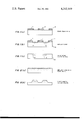
- FIG. 1 shows a partial flow chart of one embodiment of the invention.
- FIG. 2 shows a partial flow chart for another embodiment of the invention.
- the methods of the invention are similar in that they each employ ion implantation of a reactant dopant into a semiconductor substrate and use laser heating for annealing of surface ion damage of the substrate and for forming a photodetecting compound of the implanted ions and the substrate. They are different in the manner by which they delineate individual photodetectors.
- a semiconductor substrate 10 of a material such as cadmium telluride (CdTe) is bombarded through an ion-opaque mask 11 by either a flood or scanned pencil beam of mercury (Hg) ions. If a scanned beam is used, the beam may be amplitude modulated to implant ions only in desired regions and no mask will be necessary.
- CdTe cadmium telluride
- FIG. 2 shows some steps uses no mask for ion implantation but floods the entire CdTe substrate surface with ions. Those regions not desired as detectors may then be evaporated from the substrate by a high-power laser beam.
- the substrate may then be laser heated to anneal and combine as described above. Alternately, the entire surface may be laser heated to anneal and combine, then undesired portions may be evaporated by locally heating the surface.
- the evaporation and annealing-combining may be done with two different lasers, or a single laser may be varied in output power for the two operations. Moreover, evaporation and annealing-combining may be performed in a single scan of a laser beam, by varying the output power.
- This method may also use a mask on the substrate, with either a flood or pencil beam of ions.
- the same mask may be left in place while laser annealing-combining is performed, then stripped before the photodetectors are laser delineated.
- the final steps include depositing signal or readout conductors.
- the mask may be deposited by the usual techniques, such as photolithography. Moreover, the laser beam(s) of the remainder of the methods may be used to expose such masks. These same laser beams may be used (at high power) to evaporate the mask(s) after use.
- IIIA-VA compounds taken from the periodic table of elements
- GaAs in combination with other ions of the IIIA-VA class.
- the table below gives some of the possible combinations.
- a second class of compounds for which the invention is useful is the IIB-VIA compounds in combination with other ions of the IIB-VIA class.
- a typical example given in the table is CdTe(IIIB-VIA) with Hg bombardment to form Hg x Cd 1-x Te.
- the invention has thus far been limited to a single ion bombardment and annealing, more than one of each may be done. Specifically, if one wishes to make diodes, one would bombard with ions of a different conductivity type in any one of the manners described above, but with less ion energy to give less penetration. Obviously, laser annealing-combining could also be done to a shallower depth than the initial annealing. For more complex devices than diodes, more steps of ion bombarding and annealing may be performed.
Abstract
A semiconductor substrate is bombarded by ions of sufficient energy to perate the surface of the substrate to some average predetermined depth. The substrate is then scanned by a laser beam having a small diameter compared to the substrate thickness and having sufficient energy to heat the substrate to the predetermined depth. The heat allows surface damage on the substrate from the ion bombardment to heal, and allows the ions and substrate to form a compound to the predetermined depth with controllable redistribution. This compound is the photodetector of the method. The ions may be implanted through a mask to produce isolated detector regions, or the entire substrate surface may be bombarded, and those regions not desired for detector regions may be removed by a laser beam of sufficient energy to cause evaporation of a layer of the substrate. Exemplary substrate and ions are respectively cadmium telluride and mercury.
Description
The invention described herein may be manufactured, used, and licensed by the U.S. Government for governmental purposes without the payment of any royalties thereon.
This invention is in the field of focal-plane image detectors. Such detectors usually consist of a two-dimensional array of small conductor photodetectors and are made by two major methods. In the case of mercury cadmium telluride (HgCdTe) photodetectors, one method consists of bonding discrete photodetectors to a silicon substrate. The other major method consists of growing an epilayer of mercury cadmium telluride on a cadmium telluride substrate. The one method is difficult to perform with large, high-density arrays, and the other method requires steps to delineate individual detectors for crosstalk prevention. For detectors other than HgCdTe, similar methods, or other methods, may be used.
The invention is two major embodiments of a method for making a semiconductor focal plane image detector. Such a detector, when completed, includes a two-dimensional array of small photodetectors. In one embodiment the photodetectors are formed by implanting a pattern of high energy ions of a dopant into a substrate. Surface damage to the substrate from the ions is eliminated by annealing with a high-energy laser. The laser energy and wavelength are chosen such that only the ion implanted region in the substrate is heated appreciably, and not the deeper regions of the substrate. In an alternate embodiment, ions are implanted with or without a pattern into a substrate. A laser beam then evaporates the substrate to delineate individual photodetectors, and to anneal out ion damage. In both embodiments, the heat used for annealing ion damage also allows the implanted ions to combine with at least one element of the substrate to form a photodetecting compounds.
FIG. 1 shows a partial flow chart of one embodiment of the invention.
FIG. 2 shows a partial flow chart for another embodiment of the invention.
The methods of the invention are similar in that they each employ ion implantation of a reactant dopant into a semiconductor substrate and use laser heating for annealing of surface ion damage of the substrate and for forming a photodetecting compound of the implanted ions and the substrate. They are different in the manner by which they delineate individual photodetectors. In the embodiment for which FIG. 1 shows some steps, a semiconductor substrate 10, of a material such as cadmium telluride (CdTe) is bombarded through an ion-opaque mask 11 by either a flood or scanned pencil beam of mercury (Hg) ions. If a scanned beam is used, the beam may be amplitude modulated to implant ions only in desired regions and no mask will be necessary. In any event, one obtains a Gaussian distribution of Hg ions in thin regions near the surface of the CdTe. If a mask is used, one strips or otherwise removes the mask after implanting. A laser beam is then focussed into a small (with respect to desired photodetector lateral dimensions) beam and scanned over the surface of the CdTe to cause local heating. This heating melts the surface and the thin regions and induces both annealing of the surface and combination of the Hg with the CdTe to form the HgCdTe photodetectors. The usual signal or readout conductors may then be deposited on the substrate in the usual manner, such as by evaporating aluminum through a mask.
The method for which FIG. 2 shows some steps uses no mask for ion implantation but floods the entire CdTe substrate surface with ions. Those regions not desired as detectors may then be evaporated from the substrate by a high-power laser beam. The substrate may then be laser heated to anneal and combine as described above. Alternately, the entire surface may be laser heated to anneal and combine, then undesired portions may be evaporated by locally heating the surface. The evaporation and annealing-combining may be done with two different lasers, or a single laser may be varied in output power for the two operations. Moreover, evaporation and annealing-combining may be performed in a single scan of a laser beam, by varying the output power. This method may also use a mask on the substrate, with either a flood or pencil beam of ions. The same mask may be left in place while laser annealing-combining is performed, then stripped before the photodetectors are laser delineated. Whichever variation of this method is used, the final steps include depositing signal or readout conductors.
The mask, as mentioned in the methods above, may be deposited by the usual techniques, such as photolithography. Moreover, the laser beam(s) of the remainder of the methods may be used to expose such masks. These same laser beams may be used (at high power) to evaporate the mask(s) after use.
The materials for which this invention is useful comprise the IIIA-VA compounds (as taken from the periodic table of elements) such as GaAs in combination with other ions of the IIIA-VA class. The table below gives some of the possible combinations. A second class of compounds for which the invention is useful is the IIB-VIA compounds in combination with other ions of the IIB-VIA class. A typical example given in the table is CdTe(IIIB-VIA) with Hg bombardment to form Hgx Cd1-x Te.
              TABLE
______________________________________
Ion          Substrate    Detector
______________________________________
In           GaAs         Ga.sub.x In.sub.1-x
Ga           InAs         Ga.sub.x In.sub.1-x
Al           GaAsP        Ga.sub.x Al.sub.1-x AsP
Al           GaAs         Ga.sub.x Al.sub.1-x As
Ga           AlAs         Ga.sub.x Al.sub.1-x As
Hg           CdTe         Hg.sub.x Cd.sub.1-x Te
______________________________________
Although the invention has thus far been limited to a single ion bombardment and annealing, more than one of each may be done. Specifically, if one wishes to make diodes, one would bombard with ions of a different conductivity type in any one of the manners described above, but with less ion energy to give less penetration. Obviously, laser annealing-combining could also be done to a shallower depth than the initial annealing. For more complex devices than diodes, more steps of ion bombarding and annealing may be performed.
Claims (5)
1. A method of making at least one semiconductor photodetector including the steps of:
preparing a binary compound semiconductor substrate;
ion bombarding a side of said substrate in at least one predetermined area to implant ions to a predetermined depth; and
locally laser heating at least said predetermined area to said predetermined depth, whereby ion bombardment damage is healed, and whereby the implanted ions combine with at least one element of said compound to form a photodetector compound.
2. The method as recited in claim 1 wherein an entire surface of said substrate is ion bombarded, and including an additional step of:
locally laser heating said surface to evaporate said surface in a predetermined pattern to a predetermined depth.
3. Products as produced by the methods of either claim 1 or 2.
4. The method as set forth in either of claims 1 or 2 wherein the substrate is a compound of elements with at least one element taken from Group IIIA and at least one element taken from Group VA of the periodic table of elements, and the ion bombarding is performed with ions of an element chosen from the two said groups, but different from the elements of the substrate.
5. The methods as set forth in either of claims 1 or 2 wherein the substrate is a compound of elements with at least one element taken from Group IIB and at least one element taken from Group VIA of the periodic table of elements, and the ion bombarding is performed with ions of an element chosen from the two said groups, but different from the elements of the substrate.
Priority Applications (1)
| Application Number | Priority Date | Filing Date | Title |
|---|---|---|---|
| US06/062,593 US4242149A (en) | 1979-07-31 | 1979-07-31 | Method of making photodetectors using ion implantation and laser annealing |
Applications Claiming Priority (1)
| Application Number | Priority Date | Filing Date | Title |
|---|---|---|---|
| US06/062,593 US4242149A (en) | 1979-07-31 | 1979-07-31 | Method of making photodetectors using ion implantation and laser annealing |
Publications (1)
| Publication Number | Publication Date |
|---|---|
| US4242149A true US4242149A (en) | 1980-12-30 |
Family
ID=22043501
Family Applications (1)
| Application Number | Title | Priority Date | Filing Date |
|---|---|---|---|
| US06/062,593 Expired - Lifetime US4242149A (en) | 1979-07-31 | 1979-07-31 | Method of making photodetectors using ion implantation and laser annealing |
Country Status (1)
| Country | Link |
|---|---|
| US (1) | US4242149A (en) |
Cited By (20)
| Publication number | Priority date | Publication date | Assignee | Title |
|---|---|---|---|---|
| US4470192A (en) * | 1983-08-22 | 1984-09-11 | Rockwell International Corporation | Method of selected area doping of compound semiconductors |
| US4742017A (en) * | 1986-06-20 | 1988-05-03 | Ford Aerospace Corporation | Implantation method for forming Schottky barrier photodiodes |
| US4910154A (en) * | 1988-12-23 | 1990-03-20 | Ford Aerospace Corporation | Manufacture of monolithic infrared focal plane arrays |
| EP1213744A2 (en) * | 2000-12-06 | 2002-06-12 | Ulvac, Inc. | Ion implantation systems and methods |
| US20090218606A1 (en) * | 2008-02-29 | 2009-09-03 | Mccaffrey Nathaniel J | Vertically integrated light sensor and arrays |
| US20090218493A1 (en) * | 2008-02-29 | 2009-09-03 | Mccaffrey Nathaniel J | Wide spectral range hybrid image detector |
| US8680591B2 (en) | 2009-09-17 | 2014-03-25 | Sionyx, Inc. | Photosensitive imaging devices and associated methods |
| US9496308B2 (en) | 2011-06-09 | 2016-11-15 | Sionyx, Llc | Process module for increasing the response of backside illuminated photosensitive imagers and associated methods |
| US9673250B2 (en) | 2013-06-29 | 2017-06-06 | Sionyx, Llc | Shallow trench textured regions and associated methods |
| US9741761B2 (en) | 2010-04-21 | 2017-08-22 | Sionyx, Llc | Photosensitive imaging devices and associated methods |
| US9761739B2 (en) | 2010-06-18 | 2017-09-12 | Sionyx, Llc | High speed photosensitive devices and associated methods |
| US9762830B2 (en) | 2013-02-15 | 2017-09-12 | Sionyx, Llc | High dynamic range CMOS image sensor having anti-blooming properties and associated methods |
| US9905599B2 (en) | 2012-03-22 | 2018-02-27 | Sionyx, Llc | Pixel isolation elements, devices and associated methods |
| US9911781B2 (en) | 2009-09-17 | 2018-03-06 | Sionyx, Llc | Photosensitive imaging devices and associated methods |
| US9939251B2 (en) | 2013-03-15 | 2018-04-10 | Sionyx, Llc | Three dimensional imaging utilizing stacked imager devices and associated methods |
| US10244188B2 (en) | 2011-07-13 | 2019-03-26 | Sionyx, Llc | Biometric imaging devices and associated methods |
| US10361083B2 (en) | 2004-09-24 | 2019-07-23 | President And Fellows Of Harvard College | Femtosecond laser-induced formation of submicrometer spikes on a semiconductor substrate |
| US10361232B2 (en) | 2009-09-17 | 2019-07-23 | Sionyx, Llc | Photosensitive imaging devices and associated methods |
| US10374109B2 (en) | 2001-05-25 | 2019-08-06 | President And Fellows Of Harvard College | Silicon-based visible and near-infrared optoelectric devices |
| CN111987191A (en) * | 2020-09-09 | 2020-11-24 | 苏州腾晖光伏技术有限公司 | Method for repairing PERC battery laser membrane opening damage |
Citations (5)
| Publication number | Priority date | Publication date | Assignee | Title |
|---|---|---|---|---|
| DE2208271A1 (en) * | 1972-02-22 | 1973-08-30 | Anvar | METHOD AND DEVICE FOR PRODUCING SEMICONDUCTOR CONNECTIONS |
| US4081653A (en) * | 1976-12-27 | 1978-03-28 | Western Electric Co., Inc. | Removal of thin films from substrates by laser induced explosion |
| US4147563A (en) * | 1978-08-09 | 1979-04-03 | The United States Of America As Represented By The United States Department Of Energy | Method for forming p-n junctions and solar-cells by laser-beam processing |
| US4154625A (en) * | 1977-11-16 | 1979-05-15 | Bell Telephone Laboratories, Incorporated | Annealing of uncapped compound semiconductor materials by pulsed energy deposition |
| US4155779A (en) * | 1978-08-21 | 1979-05-22 | Bell Telephone Laboratories, Incorporated | Control techniques for annealing semiconductors |
-
1979
- 1979-07-31 US US06/062,593 patent/US4242149A/en not_active Expired - Lifetime
Patent Citations (5)
| Publication number | Priority date | Publication date | Assignee | Title |
|---|---|---|---|---|
| DE2208271A1 (en) * | 1972-02-22 | 1973-08-30 | Anvar | METHOD AND DEVICE FOR PRODUCING SEMICONDUCTOR CONNECTIONS |
| US4081653A (en) * | 1976-12-27 | 1978-03-28 | Western Electric Co., Inc. | Removal of thin films from substrates by laser induced explosion |
| US4154625A (en) * | 1977-11-16 | 1979-05-15 | Bell Telephone Laboratories, Incorporated | Annealing of uncapped compound semiconductor materials by pulsed energy deposition |
| US4147563A (en) * | 1978-08-09 | 1979-04-03 | The United States Of America As Represented By The United States Department Of Energy | Method for forming p-n junctions and solar-cells by laser-beam processing |
| US4155779A (en) * | 1978-08-21 | 1979-05-22 | Bell Telephone Laboratories, Incorporated | Control techniques for annealing semiconductors |
Non-Patent Citations (7)
| Title |
|---|
| Campisano et al., Solid St. Electronics, 21 (1978) 485. * |
| Donnelly et al., Appl. Phys. Letts. 20 (1972) 279. * |
| Fan et al., Appl. Phys. Letts. 34 (Jun. 1979) 780. * |
| Fiorito et al., Appl. Phys. Letts. 23 (1973) 448. * |
| Kachurin et al., Sov. Phys. Semicond. 9 (1976) 946. * |
| Marine et al., Appl. Phys. Letts. 23 (1973) 450. * |
| Martin, Nuclear Inst. & Methods, 72 (1969) 223. * |
Cited By (30)
| Publication number | Priority date | Publication date | Assignee | Title |
|---|---|---|---|---|
| US4470192A (en) * | 1983-08-22 | 1984-09-11 | Rockwell International Corporation | Method of selected area doping of compound semiconductors |
| US4742017A (en) * | 1986-06-20 | 1988-05-03 | Ford Aerospace Corporation | Implantation method for forming Schottky barrier photodiodes |
| US4910154A (en) * | 1988-12-23 | 1990-03-20 | Ford Aerospace Corporation | Manufacture of monolithic infrared focal plane arrays |
| EP1213744A2 (en) * | 2000-12-06 | 2002-06-12 | Ulvac, Inc. | Ion implantation systems and methods |
| EP1213744A3 (en) * | 2000-12-06 | 2005-12-28 | Ulvac, Inc. | Ion implantation systems and methods |
| US10374109B2 (en) | 2001-05-25 | 2019-08-06 | President And Fellows Of Harvard College | Silicon-based visible and near-infrared optoelectric devices |
| US10741399B2 (en) | 2004-09-24 | 2020-08-11 | President And Fellows Of Harvard College | Femtosecond laser-induced formation of submicrometer spikes on a semiconductor substrate |
| US10361083B2 (en) | 2004-09-24 | 2019-07-23 | President And Fellows Of Harvard College | Femtosecond laser-induced formation of submicrometer spikes on a semiconductor substrate |
| US20090218606A1 (en) * | 2008-02-29 | 2009-09-03 | Mccaffrey Nathaniel J | Vertically integrated light sensor and arrays |
| US20090218493A1 (en) * | 2008-02-29 | 2009-09-03 | Mccaffrey Nathaniel J | Wide spectral range hybrid image detector |
| US8058615B2 (en) | 2008-02-29 | 2011-11-15 | Sionyx, Inc. | Wide spectral range hybrid image detector |
| US8680591B2 (en) | 2009-09-17 | 2014-03-25 | Sionyx, Inc. | Photosensitive imaging devices and associated methods |
| US10361232B2 (en) | 2009-09-17 | 2019-07-23 | Sionyx, Llc | Photosensitive imaging devices and associated methods |
| US9911781B2 (en) | 2009-09-17 | 2018-03-06 | Sionyx, Llc | Photosensitive imaging devices and associated methods |
| US9741761B2 (en) | 2010-04-21 | 2017-08-22 | Sionyx, Llc | Photosensitive imaging devices and associated methods |
| US10229951B2 (en) | 2010-04-21 | 2019-03-12 | Sionyx, Llc | Photosensitive imaging devices and associated methods |
| US9761739B2 (en) | 2010-06-18 | 2017-09-12 | Sionyx, Llc | High speed photosensitive devices and associated methods |
| US10505054B2 (en) | 2010-06-18 | 2019-12-10 | Sionyx, Llc | High speed photosensitive devices and associated methods |
| US10269861B2 (en) | 2011-06-09 | 2019-04-23 | Sionyx, Llc | Process module for increasing the response of backside illuminated photosensitive imagers and associated methods |
| US9666636B2 (en) | 2011-06-09 | 2017-05-30 | Sionyx, Llc | Process module for increasing the response of backside illuminated photosensitive imagers and associated methods |
| US9496308B2 (en) | 2011-06-09 | 2016-11-15 | Sionyx, Llc | Process module for increasing the response of backside illuminated photosensitive imagers and associated methods |
| US10244188B2 (en) | 2011-07-13 | 2019-03-26 | Sionyx, Llc | Biometric imaging devices and associated methods |
| US10224359B2 (en) | 2012-03-22 | 2019-03-05 | Sionyx, Llc | Pixel isolation elements, devices and associated methods |
| US9905599B2 (en) | 2012-03-22 | 2018-02-27 | Sionyx, Llc | Pixel isolation elements, devices and associated methods |
| US9762830B2 (en) | 2013-02-15 | 2017-09-12 | Sionyx, Llc | High dynamic range CMOS image sensor having anti-blooming properties and associated methods |
| US9939251B2 (en) | 2013-03-15 | 2018-04-10 | Sionyx, Llc | Three dimensional imaging utilizing stacked imager devices and associated methods |
| US10347682B2 (en) | 2013-06-29 | 2019-07-09 | Sionyx, Llc | Shallow trench textured regions and associated methods |
| US9673250B2 (en) | 2013-06-29 | 2017-06-06 | Sionyx, Llc | Shallow trench textured regions and associated methods |
| US11069737B2 (en) | 2013-06-29 | 2021-07-20 | Sionyx, Llc | Shallow trench textured regions and associated methods |
| CN111987191A (en) * | 2020-09-09 | 2020-11-24 | 苏州腾晖光伏技术有限公司 | Method for repairing PERC battery laser membrane opening damage |
Similar Documents
| Publication | Publication Date | Title |
|---|---|---|
| US4242149A (en) | Method of making photodetectors using ion implantation and laser annealing | |
| US4452644A (en) | Process for doping semiconductors | |
| US4281030A (en) | Implantation of vaporized material on melted substrates | |
| US4142925A (en) | Method of making silicon-insulator-polysilicon infrared image device utilizing epitaxial deposition and selective etching | |
| US6580095B2 (en) | Circuit-containing photodetector, method of manufacturing the same, and optical device using circuit-containing photodetector | |
| US4434318A (en) | Solar cells and method | |
| US4956304A (en) | Buried junction infrared photodetector process | |
| US4270018A (en) | Amorphous solar cells | |
| US4868622A (en) | Semiconductor light-detecting device with alloyed isolating region | |
| US9397244B2 (en) | CdHgTe photodiodes array | |
| US3959038A (en) | Electron emitter and method of fabrication | |
| US4661168A (en) | Method of integrating infrared sensitive image recording element with CCD on same substrate | |
| US4319119A (en) | Process for gettering semiconductor components and integrated semiconductor circuits | |
| US3959026A (en) | Method of preparation of a semiconducting ternary alloy from the semiconducting compound ZnTe by ion | |
| US3956025A (en) | Semiconductor devices having surface state control and method of manufacture | |
| US4055443A (en) | Method for producing semiconductor matrix of light-emitting elements utilizing ion implantation and diffusion heating | |
| US4003759A (en) | Ion implantation of gold in mercury cadmium telluride | |
| JPS6259903B2 (en) | ||
| Burke et al. | High-performance visible-UV CCD imagers for space-based applications | |
| JPH05343727A (en) | Infrared detector and its manufacture | |
| USH894H (en) | IR detector structure and method of making | |
| JPS582449B2 (en) | Control method for minority carrier diffusion length | |
| US3979629A (en) | Semiconductor with surface insulator having immobile charges | |
| JPH10163517A (en) | Semiconductor device and its manufacture | |
| JP2613074B2 (en) | Method for manufacturing semiconductor device |