US4364039A - Stacked electro-optic display - Google Patents
Stacked electro-optic display Download PDFInfo
- Publication number
- US4364039A US4364039A US06/172,108 US17210880A US4364039A US 4364039 A US4364039 A US 4364039A US 17210880 A US17210880 A US 17210880A US 4364039 A US4364039 A US 4364039A
- Authority
- US
- United States
- Prior art keywords
- substrate
- cells
- liquid crystal
- electrodes
- matrix
- Prior art date
- Legal status (The legal status is an assumption and is not a legal conclusion. Google has not performed a legal analysis and makes no representation as to the accuracy of the status listed.)
- Expired - Lifetime
Links
Images

Classifications
-
- G—PHYSICS
- G09—EDUCATION; CRYPTOGRAPHY; DISPLAY; ADVERTISING; SEALS
- G09G—ARRANGEMENTS OR CIRCUITS FOR CONTROL OF INDICATING DEVICES USING STATIC MEANS TO PRESENT VARIABLE INFORMATION
- G09G3/00—Control arrangements or circuits, of interest only in connection with visual indicators other than cathode-ray tubes
- G09G3/20—Control arrangements or circuits, of interest only in connection with visual indicators other than cathode-ray tubes for presentation of an assembly of a number of characters, e.g. a page, by composing the assembly by combination of individual elements arranged in a matrix no fixed position being assigned to or needed to be assigned to the individual characters or partial characters
- G09G3/34—Control arrangements or circuits, of interest only in connection with visual indicators other than cathode-ray tubes for presentation of an assembly of a number of characters, e.g. a page, by composing the assembly by combination of individual elements arranged in a matrix no fixed position being assigned to or needed to be assigned to the individual characters or partial characters by control of light from an independent source
- G09G3/36—Control arrangements or circuits, of interest only in connection with visual indicators other than cathode-ray tubes for presentation of an assembly of a number of characters, e.g. a page, by composing the assembly by combination of individual elements arranged in a matrix no fixed position being assigned to or needed to be assigned to the individual characters or partial characters by control of light from an independent source using liquid crystals
-
- G—PHYSICS
- G02—OPTICS
- G02F—OPTICAL DEVICES OR ARRANGEMENTS FOR THE CONTROL OF LIGHT BY MODIFICATION OF THE OPTICAL PROPERTIES OF THE MEDIA OF THE ELEMENTS INVOLVED THEREIN; NON-LINEAR OPTICS; FREQUENCY-CHANGING OF LIGHT; OPTICAL LOGIC ELEMENTS; OPTICAL ANALOGUE/DIGITAL CONVERTERS
- G02F1/00—Devices or arrangements for the control of the intensity, colour, phase, polarisation or direction of light arriving from an independent light source, e.g. switching, gating or modulating; Non-linear optics
- G02F1/01—Devices or arrangements for the control of the intensity, colour, phase, polarisation or direction of light arriving from an independent light source, e.g. switching, gating or modulating; Non-linear optics for the control of the intensity, phase, polarisation or colour
- G02F1/13—Devices or arrangements for the control of the intensity, colour, phase, polarisation or direction of light arriving from an independent light source, e.g. switching, gating or modulating; Non-linear optics for the control of the intensity, phase, polarisation or colour based on liquid crystals, e.g. single liquid crystal display cells
- G02F1/133—Constructional arrangements; Operation of liquid crystal cells; Circuit arrangements
- G02F1/1333—Constructional arrangements; Manufacturing methods
- G02F1/1347—Arrangement of liquid crystal layers or cells in which the final condition of one light beam is achieved by the addition of the effects of two or more layers or cells
-
- G—PHYSICS
- G09—EDUCATION; CRYPTOGRAPHY; DISPLAY; ADVERTISING; SEALS
- G09G—ARRANGEMENTS OR CIRCUITS FOR CONTROL OF INDICATING DEVICES USING STATIC MEANS TO PRESENT VARIABLE INFORMATION
- G09G2300/00—Aspects of the constitution of display devices
- G09G2300/02—Composition of display devices
- G09G2300/023—Display panel composed of stacked panels
Definitions
- This invention relates to methods and apparatus for a visual output device which uses electro-optic cells, such as liquid crystal cells.
- electro-optic cells such as liquid crystal cells.
- Such output devices are commonly used in calculators, watches, electronic thermometers, or the like.
- an electro-optic cell e.g., a liquid crystal cell
- An electro-optic cell may be characterized as a device which will allow light or a patterned image to pass through the cell, depending on the electrical energy received. Commonly these cells use a liquid crystal material.
- multiplexing the display is essential to avoid excessive chip/display interconnections. Multiplexing involves exciting one pixel and moving quickly to another operation. Given the X-Y matrix used in multiplexing, a given pixel receives exitation signals during the whole addressing cycle, not just at the time it is specifically addressed. In order for the drive technique to work, the pixel in question must not respond to the extra signals. This means that the electro-optic response, transmission function, of the device must have a threshold characteristic. The extent to which the display turns on in a multiplex drive scheme is related to the steepness or slope of the contrast ratio vs. voltage curve above threshold.
- the contrast ratio of a liquid crystal cell as a function of voltage, past the threshold voltage is a nonlinear concave down function, as exemplified in L. A. Goodman's article, "Liquid Crystal Displays", Journal of Vacuum Science Technology, Vol. 10, No. 5, September/October 1973, page 804-8923 at 817.
- This function exemplifies the need for a disproportinate amount of voltage to achieve a given degree of darkening or opaqueing in a liquid crystal cell at a higher level of opaqueness.
- a second relevant phenomena is that a device which has a transmission function T, when put in series with a similar device will result in an overall system having a transmission function of T 2 .
- This relationship may be carried on ad infininum.
- the principle, it turns out, is applicable to the transmission function of an electro-optic cell as well.
- the transmission function is determinative of the contrast ratio.
- the present invention involves positioning two or more independent electro-optic cells in an optical series and giving each of the cells approximately simultaneous identical signals. As the light entering the optical series passes from one cell to the next, the contrast ratio is then squared, cubed, etc., until the light exits from the last cell.
- the need for approximately simultaneous signals is important for the invention.
- the optical series of cells must react identically; that is, identically within the ability of the observor to differentiate in time.
- the electrodes which define the image areas in each liquid crystal cell must be aligned so that the display will be "crisp". As they become nonaligned, the resulting display will be fuzzy or blurred since the dark part of each cell would not lie in optical series.
- optical series and associated mirrors or polarizers constitute an optical channel.
- the construction of this optical channel requires that the distance between pixels must be much less than the pixel's width. Light entering the first pixel must effectively enter the next pixel at the same relative point to achieve the optical series requirements discussed earlier.
- the invention as described is particularly applicable to multiplexing.
- the multiplex capability of a display depends on the sharpness of the transmission function.
- the transmission function is raised to a power depending on the number of displays in the stack. Anytime a nonlinear function is raised to a power algebraically, the sharpness of the function is increased. In this context then, sharpness is generalized when referring to the "slope" of the transmission function within a selected area.
- This invention allows for a much quicker rise of contrast ratio with voltage.
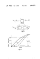
- FIGS. 1a and 1b illustrate the squaring relationship of two black boxes having identical transfer functions.
- FIG. 2 graphically shows the advantage gained through squaring and quadrupling transfer function.
- FIG. 3 is a cross section of the conceptual optical path considerations for the invention.
- FIG. 4 is a pictorial representation of a preferred embodiment of the invention.
- FIG. 5 is a pictorial representation of the invention in operation.
- I out TI in
- T 2 transformation function
- Light entering a first independent cell will be modulated by T; similarly the second cell will modulate by T as well.
- T Light entering a first independent cell
- the second cell will modulate by T as well.
- L the light entering the first cell.
- FIG. 2 graphically illustrates the advantage gained by the series relationship.
- a sine function is used only as illustrative of the degree of diffraction as a function of voltage.
- the sine function is a fair approximation to the transfer function of light past the threshold voltage.
- the function T is concave down, whereas the T 2 and T 4 functions are concave up. This means that a little increase in voltage within this zone will have more distinctive darkening for the T 2 or T 4 functions than in the T function. This change in curve structure permits added multiplexing opportunity.
- the number of cells in series is discretionary and may be carried on ad infininum, as is indicated by liquid crystal cell 34, but is practically bounded by the number of cells in series which still have a practical "on” and "off” state.
- FIG. 4 illustrates the preferred embodiment of the invention which will accomplish the above tasks.
- outer substrates 41 and 42 each have parallel electrodes embodied on them. These electrodes will form the "X" axis.
- Inner substrate 43 has embodied parallel electrodes forming the "Y” axis.
- the "Y" axis electrodes are on both sides of the inner substrate 43.
- the "X" axis electrodes are then coupled to their associated mate on the other outer substrate allowing for a signal to X 1 on the outer substrate 41 to be approximately simultaneously communicated to X 1 on the outer substrate 42.
- the Y 1 electrical lead on one surface of the inner substrate 43 is connected to the Y 1 electrode on the opposite surface.
- the X 1 electrodes of each outer substrate must be as close to being in registered alignment as possible to maximize the crispness of the display.
- the Y leads must also be in the same aligned relationship. As noted before, as the associated electrodes become nonaligned, the required optical series is diminished resulting in a blurred or fuzzy display.
- a total of XY cells may be addressed using only X+Y leads.
- a 10 ⁇ 10 matrix needs only 10+10 or 20 leads, but may address 100 electro-optic cells.
- FIG. 5 illustrates the completed invention as described in FIG. 4 in operation.
- three substrates are used, outer substrate 52, outer substrate 51 and inner substrate 53.
- the electrodes on these three substrates form the matrix having X 1 , X 2 , and X 3 as one axis while Y 1 , and Y 2 form the second axis.
- Means for multiplexing 55 may be coupled to these electrodes to provide sigals to them using multiplexing techniques known in the art.
- Observor 54, through this invention, is provided a higher contrast ratio and improved visual display.
Abstract
A visual display and method for producing the same. A plurality of electro-optic cells, such as liquid crystal cells, are placed in an optical series. Each of the cells receives approximately simultaneous identical signals. Due to the series relationship, the resulting contrast ratio will be significantly improved. The transmission function acting on the entering light will be squared after the second electro-optic cell, cubed after the third cell, etc. The enhanced transmission function has a vastly improved rise after the threshold voltage allowing for greater multiplexing capability.
Description
This invention relates to methods and apparatus for a visual output device which uses electro-optic cells, such as liquid crystal cells. Such output devices are commonly used in calculators, watches, electronic thermometers, or the like.
With the advent of hand-held devices came the need for effective visual output means which could be powered using a lower voltage than the associated desk top devices had access to utilize. The use of an electro-optic cell, e.g., a liquid crystal cell, has been widely accepted in the industry due to its ability to be constantly visible to the user, its low cost, and its relatively low power demand. An electro-optic cell may be characterized as a device which will allow light or a patterned image to pass through the cell, depending on the electrical energy received. Commonly these cells use a liquid crystal material.
For information content higher than the 23 segments in a standard digital watch display, multiplexing the display is essential to avoid excessive chip/display interconnections. Multiplexing involves exciting one pixel and moving quickly to another operation. Given the X-Y matrix used in multiplexing, a given pixel receives exitation signals during the whole addressing cycle, not just at the time it is specifically addressed. In order for the drive technique to work, the pixel in question must not respond to the extra signals. This means that the electro-optic response, transmission function, of the device must have a threshold characteristic. The extent to which the display turns on in a multiplex drive scheme is related to the steepness or slope of the contrast ratio vs. voltage curve above threshold. The sharper this transition, the more lines which can be addressed and consequently the more data that can be presented. For many nonemissive type displays, e.g., liquid crystals, the sharpness of this transfer function is poor, leading to a limited level of multiplexing and a limited information content.
Although this application addresses liquid crystal cells, the theory and applicability may be made to all electro-optic cells, a device which will permit light or an image to pass through it in relation to the externally supplied voltage.
Note initially that the contrast ratio of a liquid crystal cell as a function of voltage, past the threshold voltage, is a nonlinear concave down function, as exemplified in L. A. Goodman's article, "Liquid Crystal Displays", Journal of Vacuum Science Technology, Vol. 10, No. 5, September/October 1973, page 804-8923 at 817. This function exemplifies the need for a disproportinate amount of voltage to achieve a given degree of darkening or opaqueing in a liquid crystal cell at a higher level of opaqueness.
A second relevant phenomena is that a device which has a transmission function T, when put in series with a similar device will result in an overall system having a transmission function of T2. Hence, input of Iin will have, after the first device, output Iout =Iin T; the output after the second device in series is Iout =Iin T2. This relationship may be carried on ad infininum. The principle, it turns out, is applicable to the transmission function of an electro-optic cell as well. The transmission function is determinative of the contrast ratio.
The present invention involves positioning two or more independent electro-optic cells in an optical series and giving each of the cells approximately simultaneous identical signals. As the light entering the optical series passes from one cell to the next, the contrast ratio is then squared, cubed, etc., until the light exits from the last cell.
The need for approximately simultaneous signals is important for the invention. The optical series of cells must react identically; that is, identically within the ability of the observor to differentiate in time.
Obviously, there is some practical limit on the number of cells which can be put in optical series and still have a device with a discernable "off" and "on" state. This practical limit is controlled by the amount of absorption or scattering generated by the cell in its inactive or "off" stage. Every electro-optic cell diffuses some light, even in its "clear" state.
As those in the art will realize, to achieve the desired results, the electrodes which define the image areas in each liquid crystal cell must be aligned so that the display will be "crisp". As they become nonaligned, the resulting display will be fuzzy or blurred since the dark part of each cell would not lie in optical series.
Various modifications to the above invention are obvious to those in the art. Some of these modifications include using a means for reflection, such as a mirror, placed at the end of the optical series of cells to reflect the light back through the cells before exiting the system to some observor. Another variation involves interposing a polarizing means between the cells or using a polarizing sheet as part of the enclosure for the cell.
The above optical series and associated mirrors or polarizers constitute an optical channel. In practice, the construction of this optical channel requires that the distance between pixels must be much less than the pixel's width. Light entering the first pixel must effectively enter the next pixel at the same relative point to achieve the optical series requirements discussed earlier.
The invention as described is particularly applicable to multiplexing. As discussed above, the multiplex capability of a display depends on the sharpness of the transmission function. For a stacked display, the displays being optically independent, the transmission function is raised to a power depending on the number of displays in the stack. Anytime a nonlinear function is raised to a power algebraically, the sharpness of the function is increased. In this context then, sharpness is generalized when referring to the "slope" of the transmission function within a selected area. This invention allows for a much quicker rise of contrast ratio with voltage. For a more in-depth discussion on multiplexing techniques, refer to Jacques Robert and Bruno Dargent's article "Multiplexing Techniques for Liquid-Crystal Displays", IEEE Transactions on Electron Devices, Vol. Ed-24, No. 6, June 1977, Pages 694-697.
The invention, together with the beforementioned principles will be more fully explained by the following figures and their accompanying descriptions.
FIGS. 1a and 1b illustrate the squaring relationship of two black boxes having identical transfer functions.
FIG. 2 graphically shows the advantage gained through squaring and quadrupling transfer function.
FIG. 3 is a cross section of the conceptual optical path considerations for the invention.
FIG. 4 is a pictorial representation of a preferred embodiment of the invention.
FIG. 5 is a pictorial representation of the invention in operation.
Specifically in FIG. 1a, black box 11 has a transfer function, T. That is to say, input 12, Iin, will be transformed to give an output 13, Iout, defined by the function Iout =TIin. By then placing two black boxes 11 in series, as illustrated in FIG. 1b, the output will be defined in the function Iout =T2 Iin. These two black boxes 11 then form a system 14 which has a transformation function T2. This general principle is true for an optical transfer function in series as well as electrical functions set in series.
Light entering a first independent cell will be modulated by T; similarly the second cell will modulate by T as well. As example: suppose each cell has an 80% transmission, light exiting the first cell is (0.80)L where L is the light entering the first cell. This (0.80)L enters the second cell which modulates the light again by 80% resulting in (0.80) (0.80)L=(0.80)2 L exiting the series.
FIG. 2 graphically illustrates the advantage gained by the series relationship. A sine function is used only as illustrative of the degree of diffraction as a function of voltage. The sine function is a fair approximation to the transfer function of light past the threshold voltage.
Within the practical "On" zone 21, the function T is concave down, whereas the T2 and T4 functions are concave up. This means that a little increase in voltage within this zone will have more distinctive darkening for the T2 or T4 functions than in the T function. This change in curve structure permits added multiplexing opportunity.
In FIG. 3, light ray 33 enters the top electro-optic display cell 31 and then passes through to a second electro-optic cell 32. To keep the beam of light passing through the same relative points, the pixel to pixel distance, d, must be much less than the pixel width, D. It has been determined that values of d=10 mils and D=25 mils will produce acceptable results. These two results are given only as examples of values for which the invention will work and are not to be restricting or limiting upon the invention.
The number of cells in series is discretionary and may be carried on ad infininum, as is indicated by liquid crystal cell 34, but is practically bounded by the number of cells in series which still have a practical "on" and "off" state.
Intrinsic to the invention is that each of the cells in the optical channel receives approximately simultaneous identical signals. FIG. 4 illustrates the preferred embodiment of the invention which will accomplish the above tasks.
In FIG. 4, outer substrates 41 and 42 each have parallel electrodes embodied on them. These electrodes will form the "X" axis. Inner substrate 43 has embodied parallel electrodes forming the "Y" axis. The "Y" axis electrodes are on both sides of the inner substrate 43. Through cavity regions or other methods known to those in the art, a quantity of liquid crystal material is maintained between the outer substrates and the inner substrate while the three substrates are sealed to each other. The direction of sealing is indicated by arrows 44. The liquid crystal material is not illustrated in this drawing, nor is the means for sealing.
The "X" axis electrodes are then coupled to their associated mate on the other outer substrate allowing for a signal to X1 on the outer substrate 41 to be approximately simultaneously communicated to X1 on the outer substrate 42. Similarly, the Y1 electrical lead on one surface of the inner substrate 43 is connected to the Y1 electrode on the opposite surface. The X1 electrodes of each outer substrate must be as close to being in registered alignment as possible to maximize the crispness of the display. Similarly the Y leads must also be in the same aligned relationship. As noted before, as the associated electrodes become nonaligned, the required optical series is diminished resulting in a blurred or fuzzy display.
By having a matrix of X by Y leads, a total of XY cells may be addressed using only X+Y leads. By way of example then, a 10×10 matrix needs only 10+10 or 20 leads, but may address 100 electro-optic cells.
The use of three substrates, as discussed above, may be optimum but it is not controlling upon the invention. Two independent cells may be connected to each other to produce the identical result. In this method then, four substrates are used, two for each cell. Apparent from this is that the actual number of substrates used in the invention is open to selection by the designer.
FIG. 5 illustrates the completed invention as described in FIG. 4 in operation. Again, three substrates are used, outer substrate 52, outer substrate 51 and inner substrate 53. Note again that the use of three substrates is not critical to the invention which may have multiple substrates including four. The electrodes on these three substrates form the matrix having X1, X2, and X3 as one axis while Y1, and Y2 form the second axis. Means for multiplexing 55 may be coupled to these electrodes to provide sigals to them using multiplexing techniques known in the art. Observor 54, through this invention, is provided a higher contrast ratio and improved visual display.
Claims (4)
1. A matrix of liquid crystal cells comprising:
(a) A center substrate having a first and opposite second surface, said first surface having a plurality of first surface electrodes connected to a plurality of second surface electrodes contained on said second surface and aligned to the first surface electrodes, said center substrate comprising polarizing material;
(b) a quantity of first liquid crystal material maintained on said first surface of said center substrate;
(c) a first substrate having a first surface containing a plurality of electrodes, said first surface of said first substrate disposed to enclose the first liquid crystal material between the center substrate and the first substrate;
(d) a quantity of second liquid crystal material maintained on said second surface of said center substrate;
(e) a second substrate having a first surface and opposite second surface, said first surface containing a plurality of electrodes, said first surface of said second substrate disposed to enclose the second liquid crystal material between the center substrate and the second substrate, and disposed so that each of the electrodes on the first substrate is aligned to an aligned electrode in the plurality of electrodes on the second substrate;
(f) means for sealing applied around the perimeter of said center substrate applied so that the first substrate is sealed to the center substrate and the second substrate is sealed to the center substrate; and,
(g) means for electrically connecting each electrode on said first substrate to the aligned electrode on said second substrate.
2. A matrix of liquid crystal cells as claimed in claim 1 further comprised of a means for multiplexing connected to each of the electrodes on said first substrate and to each of the electrodes on the first surface of said center substrate.
3. A matrix of liquid crystal cells as claimed in claim 1 or 2 further comprised of a means for reflection disposed to said second surface of the second substrate so that light impinging on said means for reflection is reflected back through the second substrate.
4. A graphic display comprising:
first and second matrices of LCD cells; each said matrix of LCD cells comprising:
a plurality of liquid crystal cells, said cells being arranged in rows and columns;
a plurality of row conductors, each of said row conductors being connected to all of said cells in a corresponding one of said rows of said respective matrix;
a plurality of column conductors, each of said column conductors being connected to all of said cells in a corresponding one of said columns of said respective matrix;
said first and second matrices being parallel and closely adjacent, and respective rows and columns of said cells of said first one of said matrices being parallel to and adjacent to corresponding ones of said rows and columns of said second matrix;
polarizing means interposed between said respective first and second matrices;
means for driving corresponding row conductors of said first and second matrices in mutual synchrony; and
means for driving corresponding column conductors of said first and second matrices in mutual synchrony.
Priority Applications (2)
| Application Number | Priority Date | Filing Date | Title |
|---|---|---|---|
| US06/172,108 US4364039A (en) | 1980-07-25 | 1980-07-25 | Stacked electro-optic display |
| US06/341,976 US4547043A (en) | 1980-07-25 | 1982-01-22 | Stacked LCD graphics display |
Applications Claiming Priority (1)
| Application Number | Priority Date | Filing Date | Title |
|---|---|---|---|
| US06/172,108 US4364039A (en) | 1980-07-25 | 1980-07-25 | Stacked electro-optic display |
Related Child Applications (1)
| Application Number | Title | Priority Date | Filing Date |
|---|---|---|---|
| US06/341,976 Continuation-In-Part US4547043A (en) | 1980-07-25 | 1982-01-22 | Stacked LCD graphics display |
Publications (1)
| Publication Number | Publication Date |
|---|---|
| US4364039A true US4364039A (en) | 1982-12-14 |
Family
ID=22626393
Family Applications (1)
| Application Number | Title | Priority Date | Filing Date |
|---|---|---|---|
| US06/172,108 Expired - Lifetime US4364039A (en) | 1980-07-25 | 1980-07-25 | Stacked electro-optic display |
Country Status (1)
| Country | Link |
|---|---|
| US (1) | US4364039A (en) |
Cited By (36)
| Publication number | Priority date | Publication date | Assignee | Title |
|---|---|---|---|---|
| US4495492A (en) * | 1982-05-05 | 1985-01-22 | Litton Systems, Inc. | Magneto-optic chip with gray-scale capability |
| US4508427A (en) * | 1982-10-22 | 1985-04-02 | International Standard Electric Corporation | Liquid crystal display device |
| US4516834A (en) * | 1983-04-08 | 1985-05-14 | Rockwell International Corporation | Contrast enhanced liquid crystal display |
| US4547043A (en) * | 1980-07-25 | 1985-10-15 | Penz Perry A | Stacked LCD graphics display |
| US4601537A (en) * | 1984-01-06 | 1986-07-22 | Ohio State University Research Foundation | Apparatus and methods for forming images and for optical demultiplexing |
| FR2584521A1 (en) * | 1985-07-02 | 1987-01-09 | Renault | ELECTRO-OPTICAL DISPLAY DEVICE WITH LIQUID CRYSTAL |
| US4661809A (en) * | 1982-05-05 | 1987-04-28 | Litton Systems, Inc. | Magneto-optic chip with gray-scale capability |
| US4693560A (en) * | 1986-09-25 | 1987-09-15 | Taliq Corporation | Double layer display |
| US4698668A (en) * | 1982-08-30 | 1987-10-06 | Canadian Industrial Innovation Centre/Waterloo | Apparatus for influencing the presentation of visual information |
| WO1987007395A1 (en) * | 1986-05-20 | 1987-12-03 | Battelle Development Corporation | Method and device for enhancing the visual contrast in matrix liquid crystal displays |
| US4902105A (en) * | 1984-09-19 | 1990-02-20 | U.S. Philips Corporation | Liquid crystal display device |
| US4927240A (en) * | 1983-11-02 | 1990-05-22 | Michael Stolov | Multiple liquid crystal display |
| US5920298A (en) * | 1996-12-19 | 1999-07-06 | Colorado Microdisplay, Inc. | Display system having common electrode modulation |
| US6046716A (en) * | 1996-12-19 | 2000-04-04 | Colorado Microdisplay, Inc. | Display system having electrode modulation to alter a state of an electro-optic layer |
| US6078303A (en) * | 1996-12-19 | 2000-06-20 | Colorado Microdisplay, Inc. | Display system having electrode modulation to alter a state of an electro-optic layer |
| US20020090184A1 (en) * | 2000-12-20 | 2002-07-11 | Michel Sayag | Light stimulating and collecting methods and apparatus for storage-phosphor image plates |
| US20030025869A1 (en) * | 2001-05-11 | 2003-02-06 | Deary Randall J. | Liquid crystal assembly and method of making |
| WO2003016998A1 (en) * | 2001-08-17 | 2003-02-27 | Michel Sayag | Dual-stage high-contrast electronic image display |
| WO2004051994A1 (en) | 2002-12-04 | 2004-06-17 | Thomson Licensing S. A. | High contrast stereoscopic projection system |
| US20050162737A1 (en) * | 2002-03-13 | 2005-07-28 | Whitehead Lorne A. | High dynamic range display devices |
| US20050206582A1 (en) * | 2001-11-09 | 2005-09-22 | Bell Gareth P | Depth fused display |
| JP2005531796A (en) * | 2002-06-25 | 2005-10-20 | ピュアー デプス リミテッド | Display highlighting technology through local dynamic control of background illumination level |
| US20070132956A1 (en) * | 2001-02-27 | 2007-06-14 | The University Of British Columbia | High dynamic range display devices |
| US20080284792A1 (en) * | 2007-05-18 | 2008-11-20 | Gareth Paul Bell | Method and system for improving display quality of a multi-component display |
| US20090213141A1 (en) * | 2005-10-05 | 2009-08-27 | Puredepth Limited | Method of manipulating visibility of images on a volumetric display |
| US20100002026A1 (en) * | 2007-02-01 | 2010-01-07 | Dolby Laboratories Licensing Corporation | Calibration of displays having spatially-variable backlight |
| US20100214282A1 (en) * | 2009-02-24 | 2010-08-26 | Dolby Laboratories Licensing Corporation | Apparatus for providing light source modulation in dual modulator displays |
| US20100289819A1 (en) * | 2009-05-14 | 2010-11-18 | Pure Depth Limited | Image manipulation |
| US20110007089A1 (en) * | 2009-07-07 | 2011-01-13 | Pure Depth Limited | Method and system of processing images for improved display |
| US20110267279A1 (en) * | 2010-04-29 | 2011-11-03 | Apple Inc. | Power efficient organic light emitting diode display |
| US8146277B2 (en) | 2002-09-20 | 2012-04-03 | Puredepth Limited | Multi-view display |
| US8154473B2 (en) | 2003-05-16 | 2012-04-10 | Pure Depth Limited | Display control system |
| US8482698B2 (en) | 2008-06-25 | 2013-07-09 | Dolby Laboratories Licensing Corporation | High dynamic range display using LED backlighting, stacked optical films, and LCD drive signals based on a low resolution light field simulation |
| US8687271B2 (en) | 2002-03-13 | 2014-04-01 | Dolby Laboratories Licensing Corporation | N-modulation displays and related methods |
| US20140267203A1 (en) * | 2013-03-18 | 2014-09-18 | Venkataraman Ramanathan | Glare reduction system |
| US9448449B2 (en) | 2013-01-31 | 2016-09-20 | Venkataraman Ramanathan | Glare reduction system |
Citations (11)
| Publication number | Priority date | Publication date | Assignee | Title |
|---|---|---|---|---|
| US3655269A (en) * | 1971-01-25 | 1972-04-11 | Rca Corp | Liquid crystal display assembly having independent contrast and speed of response controls |
| US3661444A (en) * | 1969-12-02 | 1972-05-09 | Rca Corp | Compounded liquid crystal cells |
| US3873186A (en) * | 1973-09-18 | 1975-03-25 | Motorola Inc | Liquid crystal display |
| US3977767A (en) * | 1974-07-23 | 1976-08-31 | Dai Nippon Insatsu Kabushiki Kaisha | Electro-optical cell |
| US3982239A (en) * | 1973-02-07 | 1976-09-21 | North Hills Electronics, Inc. | Saturation drive arrangements for optically bistable displays |
| US3992082A (en) * | 1974-01-29 | 1976-11-16 | Siemens Aktiengesellschaft | Compound liquid crystal indicator screen |
| US4039254A (en) * | 1976-05-27 | 1977-08-02 | Mack Gordon | Electro-optic welding lens assembly using multiple liquid crystal light shutters and polarizers |
| US4099855A (en) * | 1975-10-04 | 1978-07-11 | The Marconi Company Limited | Liquid crystal display arrangements |
| US4231640A (en) * | 1977-07-07 | 1980-11-04 | Sharp Kabushiki Kaisha | Matrix type liquid crystal display panel |
| US4232948A (en) * | 1973-07-18 | 1980-11-11 | Secretary Of State For Defence | Liquid crystal display device |
| US4241339A (en) * | 1977-02-16 | 1980-12-23 | Kabushiki Kaisha Suwa Seikosha | Multi-colored display device |
-
1980
- 1980-07-25 US US06/172,108 patent/US4364039A/en not_active Expired - Lifetime
Patent Citations (11)
| Publication number | Priority date | Publication date | Assignee | Title |
|---|---|---|---|---|
| US3661444A (en) * | 1969-12-02 | 1972-05-09 | Rca Corp | Compounded liquid crystal cells |
| US3655269A (en) * | 1971-01-25 | 1972-04-11 | Rca Corp | Liquid crystal display assembly having independent contrast and speed of response controls |
| US3982239A (en) * | 1973-02-07 | 1976-09-21 | North Hills Electronics, Inc. | Saturation drive arrangements for optically bistable displays |
| US4232948A (en) * | 1973-07-18 | 1980-11-11 | Secretary Of State For Defence | Liquid crystal display device |
| US3873186A (en) * | 1973-09-18 | 1975-03-25 | Motorola Inc | Liquid crystal display |
| US3992082A (en) * | 1974-01-29 | 1976-11-16 | Siemens Aktiengesellschaft | Compound liquid crystal indicator screen |
| US3977767A (en) * | 1974-07-23 | 1976-08-31 | Dai Nippon Insatsu Kabushiki Kaisha | Electro-optical cell |
| US4099855A (en) * | 1975-10-04 | 1978-07-11 | The Marconi Company Limited | Liquid crystal display arrangements |
| US4039254A (en) * | 1976-05-27 | 1977-08-02 | Mack Gordon | Electro-optic welding lens assembly using multiple liquid crystal light shutters and polarizers |
| US4241339A (en) * | 1977-02-16 | 1980-12-23 | Kabushiki Kaisha Suwa Seikosha | Multi-colored display device |
| US4231640A (en) * | 1977-07-07 | 1980-11-04 | Sharp Kabushiki Kaisha | Matrix type liquid crystal display panel |
Non-Patent Citations (1)
| Title |
|---|
| Alt and Pleshko, "Scanning Limitations of Liquid-Crystal Displays", IEEE Transactions on Electron Devices, vol. ED-21, No. 2, Feb. 1974, pp. 146-155. * |
Cited By (110)
| Publication number | Priority date | Publication date | Assignee | Title |
|---|---|---|---|---|
| US4547043A (en) * | 1980-07-25 | 1985-10-15 | Penz Perry A | Stacked LCD graphics display |
| US4495492A (en) * | 1982-05-05 | 1985-01-22 | Litton Systems, Inc. | Magneto-optic chip with gray-scale capability |
| US4661809A (en) * | 1982-05-05 | 1987-04-28 | Litton Systems, Inc. | Magneto-optic chip with gray-scale capability |
| US4698668A (en) * | 1982-08-30 | 1987-10-06 | Canadian Industrial Innovation Centre/Waterloo | Apparatus for influencing the presentation of visual information |
| US4508427A (en) * | 1982-10-22 | 1985-04-02 | International Standard Electric Corporation | Liquid crystal display device |
| US4516834A (en) * | 1983-04-08 | 1985-05-14 | Rockwell International Corporation | Contrast enhanced liquid crystal display |
| US4927240A (en) * | 1983-11-02 | 1990-05-22 | Michael Stolov | Multiple liquid crystal display |
| US4601537A (en) * | 1984-01-06 | 1986-07-22 | Ohio State University Research Foundation | Apparatus and methods for forming images and for optical demultiplexing |
| US4902105A (en) * | 1984-09-19 | 1990-02-20 | U.S. Philips Corporation | Liquid crystal display device |
| FR2584521A1 (en) * | 1985-07-02 | 1987-01-09 | Renault | ELECTRO-OPTICAL DISPLAY DEVICE WITH LIQUID CRYSTAL |
| EP0209439A1 (en) * | 1985-07-02 | 1987-01-21 | Regie Nationale Des Usines Renault | Electro-optical display device with liquid crystals |
| WO1987007395A1 (en) * | 1986-05-20 | 1987-12-03 | Battelle Development Corporation | Method and device for enhancing the visual contrast in matrix liquid crystal displays |
| US4693560A (en) * | 1986-09-25 | 1987-09-15 | Taliq Corporation | Double layer display |
| WO1988002499A1 (en) * | 1986-09-25 | 1988-04-07 | Taliq Corporation | Double layer display |
| US5920298A (en) * | 1996-12-19 | 1999-07-06 | Colorado Microdisplay, Inc. | Display system having common electrode modulation |
| US6046716A (en) * | 1996-12-19 | 2000-04-04 | Colorado Microdisplay, Inc. | Display system having electrode modulation to alter a state of an electro-optic layer |
| US6078303A (en) * | 1996-12-19 | 2000-06-20 | Colorado Microdisplay, Inc. | Display system having electrode modulation to alter a state of an electro-optic layer |
| US6104367A (en) * | 1996-12-19 | 2000-08-15 | Colorado Microdisplay, Inc. | Display system having electrode modulation to alter a state of an electro-optic layer |
| US6144353A (en) * | 1996-12-19 | 2000-11-07 | Colorado Microdisplay, Inc. | Display system having electrode modulation to alter a state of an electro-optic layer |
| US6304239B1 (en) | 1996-12-19 | 2001-10-16 | Zight Corporation | Display system having electrode modulation to alter a state of an electro-optic layer |
| US6329971B2 (en) | 1996-12-19 | 2001-12-11 | Zight Corporation | Display system having electrode modulation to alter a state of an electro-optic layer |
| US20020090184A1 (en) * | 2000-12-20 | 2002-07-11 | Michel Sayag | Light stimulating and collecting methods and apparatus for storage-phosphor image plates |
| US20060273262A1 (en) * | 2000-12-20 | 2006-12-07 | Michel Sayag | Light stimulating and collecting methods and apparatus for storage-phosphor image plates |
| US7825394B2 (en) | 2000-12-20 | 2010-11-02 | Michel Sayag | Light stimulating and collecting methods and apparatus for storage-phosphor image plates |
| US7589341B2 (en) | 2000-12-20 | 2009-09-15 | Michel Sayag | Light stimulating and collecting methods and apparatus for storage-phosphor image plates |
| US20040164257A1 (en) * | 2000-12-20 | 2004-08-26 | Michel Sayag | Light stimulating and collecting methods and apparatus for storage-phosphor image plates |
| US6800870B2 (en) | 2000-12-20 | 2004-10-05 | Michel Sayag | Light stimulating and collecting methods and apparatus for storage-phosphor image plates |
| US20090173899A1 (en) * | 2000-12-20 | 2009-07-09 | Michel Sayag | Light stimulating and collecting methods and apparatus for storage-phosphor image plates |
| US8419194B2 (en) | 2001-02-27 | 2013-04-16 | Dolby Laboratories Licensing Corporation | Locally dimmed display |
| US20110216387A1 (en) * | 2001-02-27 | 2011-09-08 | Dolby Laboratories Licensing Corporation | Edge lit locally dimmed display |
| US10261405B2 (en) | 2001-02-27 | 2019-04-16 | Dolby Laboratories Licensing Corporation | Projection displays |
| US9804487B2 (en) | 2001-02-27 | 2017-10-31 | Dolby Laboratories Licensing Corporation | Projection displays |
| US9412337B2 (en) | 2001-02-27 | 2016-08-09 | Dolby Laboratories Licensing Corporation | Projection displays |
| US8684533B2 (en) | 2001-02-27 | 2014-04-01 | Dolby Laboratories Licensing Corporation | Projection displays |
| US8408718B2 (en) | 2001-02-27 | 2013-04-02 | Dolby Laboratories Licensing Corporation | Locally dimmed display |
| US8277056B2 (en) * | 2001-02-27 | 2012-10-02 | Dolby Laboratories Licensing Corporation | Locally dimmed display |
| US20120188296A1 (en) * | 2001-02-27 | 2012-07-26 | Dolby Laboratories Licensing Corporation | Locally dimmed display |
| US8172401B2 (en) | 2001-02-27 | 2012-05-08 | Dolby Laboratories Licensing Corporation | Edge lit locally dimmed display |
| US7942531B2 (en) | 2001-02-27 | 2011-05-17 | Dolby Laboratories Licensing Corporation | Edge lit locally dimmed display |
| US20070132956A1 (en) * | 2001-02-27 | 2007-06-14 | The University Of British Columbia | High dynamic range display devices |
| US20070268577A1 (en) * | 2001-02-27 | 2007-11-22 | Dolby Canada Corporation | Hdr displays having location specific modulation |
| US20100302480A1 (en) * | 2001-02-27 | 2010-12-02 | Lorne Whitehead | Edge lit locally dimmed display |
| US7801426B2 (en) | 2001-02-27 | 2010-09-21 | Dolby Laboratories Licensing Corporation | High dynamic range display devices having color light sources |
| US7753530B2 (en) | 2001-02-27 | 2010-07-13 | Dolby Laboratories Licensing Corporation | HDR displays and control systems therefor |
| US7377652B2 (en) | 2001-02-27 | 2008-05-27 | Dolby Laboratories Licensing Corporation | HDR displays having location specific modulation |
| US7581837B2 (en) | 2001-02-27 | 2009-09-01 | Dolby Laboratories Licensing Corporation | HDR displays and control systems therefor |
| US20080174614A1 (en) * | 2001-02-27 | 2008-07-24 | Dolby Laboratories Licensing Corporation | High dynamic range display devices |
| US7413307B2 (en) | 2001-02-27 | 2008-08-19 | Dolby Laboratories Licensing Corporation | High dynamic range display devices |
| US7413309B2 (en) | 2001-02-27 | 2008-08-19 | Dolby Laboratories Licensing Corporation | High dynamic range display devices |
| US7419267B2 (en) | 2001-02-27 | 2008-09-02 | Dolby Laboratories Licensing Corporation | HDR displays with overlapping dual modulation |
| US20090180078A1 (en) * | 2001-02-27 | 2009-07-16 | Lorne Whitehead | High dynamic range display devices having color light sources |
| US20030025869A1 (en) * | 2001-05-11 | 2003-02-06 | Deary Randall J. | Liquid crystal assembly and method of making |
| US7136136B2 (en) | 2001-05-11 | 2006-11-14 | Cambridge Research And Instrumentation, Inc. | Liquid crystal assembly and method of making |
| US6927834B2 (en) | 2001-05-11 | 2005-08-09 | Cambridge Research And Instrumentation, Inc. | Liquid crystal assembly and method of making |
| US20050134792A1 (en) * | 2001-05-11 | 2005-06-23 | Deary Randall J. | Liquid crystal assembly and method of making |
| US7002533B2 (en) | 2001-08-17 | 2006-02-21 | Michel Sayag | Dual-stage high-contrast electronic image display |
| WO2003016998A1 (en) * | 2001-08-17 | 2003-02-27 | Michel Sayag | Dual-stage high-contrast electronic image display |
| US20050206582A1 (en) * | 2001-11-09 | 2005-09-22 | Bell Gareth P | Depth fused display |
| US7619585B2 (en) | 2001-11-09 | 2009-11-17 | Puredepth Limited | Depth fused display |
| US7370979B2 (en) | 2002-03-13 | 2008-05-13 | Dolby Laboratories Licensing Corporation | Calibration of displays having spatially-variable backlight |
| US8199401B2 (en) | 2002-03-13 | 2012-06-12 | Dolby Laboratories Licensing Corporation | N-modulation displays and related methods |
| US9270956B2 (en) | 2002-03-13 | 2016-02-23 | Dolby Laboratories Licensing Corporation | Image display |
| US7800822B2 (en) | 2002-03-13 | 2010-09-21 | Dolby Laboratories Licensing Corporation | HDR displays with individually-controllable color backlights |
| US7777945B2 (en) | 2002-03-13 | 2010-08-17 | Dolby Laboratories Licensing Corporation | HDR displays having light estimating controllers |
| US20050162737A1 (en) * | 2002-03-13 | 2005-07-28 | Whitehead Lorne A. | High dynamic range display devices |
| US8446351B2 (en) | 2002-03-13 | 2013-05-21 | Dolby Laboratories Licensing Corporation | Edge lit LED based locally dimmed display |
| US20100007577A1 (en) * | 2002-03-13 | 2010-01-14 | Ajit Ninan | N-modulation displays and related methods |
| US8890799B2 (en) | 2002-03-13 | 2014-11-18 | Dolby Laboratories Licensing Corporation | Display with red, green, and blue light sources |
| US20080018985A1 (en) * | 2002-03-13 | 2008-01-24 | Dolby Canada Corporation | Hdr displays having light estimating controllers |
| US7403332B2 (en) | 2002-03-13 | 2008-07-22 | Dolby Laboratories Licensing Corporation | High dynamic range display devices |
| US10416480B2 (en) | 2002-03-13 | 2019-09-17 | Dolby Laboratories Licensing Corporation | Image display |
| US11378840B2 (en) | 2002-03-13 | 2022-07-05 | Dolby Laboratories Licensing Corporation | Image display |
| US8059110B2 (en) | 2002-03-13 | 2011-11-15 | Dolby Laboratories Licensing Corporation | Motion-blur compensation in backlit displays |
| US8125425B2 (en) | 2002-03-13 | 2012-02-28 | Dolby Laboratories Licensing Corporation | HDR displays with dual modulators having different resolutions |
| US8687271B2 (en) | 2002-03-13 | 2014-04-01 | Dolby Laboratories Licensing Corporation | N-modulation displays and related methods |
| US20060125745A1 (en) * | 2002-06-25 | 2006-06-15 | Evanicky Daniel E | Enhanced viewing experience of a display through localised dynamic control of background lighting level |
| US8416149B2 (en) * | 2002-06-25 | 2013-04-09 | Pure Depth Limited | Enhanced viewing experience of a display through localised dynamic control of background lighting level |
| JP2005531796A (en) * | 2002-06-25 | 2005-10-20 | ピュアー デプス リミテッド | Display highlighting technology through local dynamic control of background illumination level |
| US8146277B2 (en) | 2002-09-20 | 2012-04-03 | Puredepth Limited | Multi-view display |
| JP2006509242A (en) * | 2002-12-04 | 2006-03-16 | トムソン ライセンシング | High contrast stereo projection system |
| US7192139B2 (en) | 2002-12-04 | 2007-03-20 | Thomson Licensing | High contrast stereoscopic projection system |
| US20060082731A1 (en) * | 2002-12-04 | 2006-04-20 | Valter Drazic | High contrast stereoscopic projection system |
| KR101019378B1 (en) * | 2002-12-04 | 2011-03-07 | 톰슨 라이센싱 | High contrast stereoscopic projection system |
| WO2004051994A1 (en) | 2002-12-04 | 2004-06-17 | Thomson Licensing S. A. | High contrast stereoscopic projection system |
| CN100384239C (en) * | 2002-12-04 | 2008-04-23 | 汤姆森许可贸易公司 | High contrast stereoscopic projection system |
| US8154473B2 (en) | 2003-05-16 | 2012-04-10 | Pure Depth Limited | Display control system |
| US9292150B2 (en) | 2003-05-16 | 2016-03-22 | Pure Depth Limited | Display control system |
| US20090213141A1 (en) * | 2005-10-05 | 2009-08-27 | Puredepth Limited | Method of manipulating visibility of images on a volumetric display |
| US8436873B2 (en) | 2005-10-05 | 2013-05-07 | Pure Depth Limited | Method of manipulating visibility of images on a volumetric display |
| US20100002026A1 (en) * | 2007-02-01 | 2010-01-07 | Dolby Laboratories Licensing Corporation | Calibration of displays having spatially-variable backlight |
| US8471807B2 (en) | 2007-02-01 | 2013-06-25 | Dolby Laboratories Licensing Corporation | Calibration of displays having spatially-variable backlight |
| US8432411B2 (en) | 2007-05-18 | 2013-04-30 | Pure Depth Limited | Method and system for improving display quality of a multi-component display |
| US20080284792A1 (en) * | 2007-05-18 | 2008-11-20 | Gareth Paul Bell | Method and system for improving display quality of a multi-component display |
| US10607569B2 (en) | 2008-06-25 | 2020-03-31 | Dolby Laboratories Licensing Corporation | High dynamic range display using LED backlighting, stacked optical films, and LCD drive signals based on a low resolution light field simulation |
| US8482698B2 (en) | 2008-06-25 | 2013-07-09 | Dolby Laboratories Licensing Corporation | High dynamic range display using LED backlighting, stacked optical films, and LCD drive signals based on a low resolution light field simulation |
| US9711111B2 (en) | 2008-06-25 | 2017-07-18 | Dolby Laboratories Licensing Corporation | High dynamic range display using LED backlighting, stacked optical films, and LCD drive signals based on a low resolution light field simulation |
| US10373574B2 (en) | 2009-02-24 | 2019-08-06 | Dolby Laboratories Licensing Corporation | Locally dimmed quantum dot display |
| US9911389B2 (en) | 2009-02-24 | 2018-03-06 | Dolby Laboratories Licensing Corporation | Locally dimmed quantum dot display |
| US9099046B2 (en) | 2009-02-24 | 2015-08-04 | Dolby Laboratories Licensing Corporation | Apparatus for providing light source modulation in dual modulator displays |
| US20100214282A1 (en) * | 2009-02-24 | 2010-08-26 | Dolby Laboratories Licensing Corporation | Apparatus for providing light source modulation in dual modulator displays |
| US9478182B2 (en) | 2009-02-24 | 2016-10-25 | Dolby Laboratories Licensing Corporation | Locally dimmed quantum dots (nano-crystal) based display |
| US9524700B2 (en) | 2009-05-14 | 2016-12-20 | Pure Depth Limited | Method and system for displaying images of various formats on a single display |
| US20100289819A1 (en) * | 2009-05-14 | 2010-11-18 | Pure Depth Limited | Image manipulation |
| US8928682B2 (en) | 2009-07-07 | 2015-01-06 | Pure Depth Limited | Method and system of processing images for improved display |
| US20110007089A1 (en) * | 2009-07-07 | 2011-01-13 | Pure Depth Limited | Method and system of processing images for improved display |
| US9087801B2 (en) * | 2010-04-29 | 2015-07-21 | Apple Inc. | Power efficient organic light emitting diode display |
| US20110267279A1 (en) * | 2010-04-29 | 2011-11-03 | Apple Inc. | Power efficient organic light emitting diode display |
| US9448449B2 (en) | 2013-01-31 | 2016-09-20 | Venkataraman Ramanathan | Glare reduction system |
| US9601083B2 (en) * | 2013-03-18 | 2017-03-21 | Venkataraman Ramanathan | Glare reduction system |
| US20140267203A1 (en) * | 2013-03-18 | 2014-09-18 | Venkataraman Ramanathan | Glare reduction system |
Similar Documents
| Publication | Publication Date | Title |
|---|---|---|
| US4364039A (en) | Stacked electro-optic display | |
| US4547043A (en) | Stacked LCD graphics display | |
| US5488498A (en) | Liquid crystal display with particular contacts for supplying counter electrode potential | |
| US4549174A (en) | Electrode terminal assembly on a multi-layer type liquid crystal panel | |
| US5404236A (en) | Display device with crossing electrodes with specific ratio for gray scale | |
| DE69928621T2 (en) | Drive circuit for transflective liquid crystal display and liquid crystal display | |
| TW354379B (en) | Liquid crystal display | |
| EP0372821A3 (en) | Liquid crystal display panel with reduced pixel defects | |
| EP0369621A3 (en) | Liquid crystal display device | |
| JP2959509B2 (en) | Liquid crystal display | |
| JPH052969B2 (en) | ||
| JP3022646B2 (en) | Display device | |
| EP1407318B1 (en) | Colour liquid crystal display device with electrically switchable colour filters | |
| US4904057A (en) | Liquid crystal device with a smectic chiral liquid crystal and with a rectifier in series with each pixel | |
| JP2689518B2 (en) | Electro-optical device and driving method thereof | |
| US20100014038A1 (en) | Black and White Color Cholesteric Liquid Crystal Display | |
| US4759609A (en) | Process for the sequential control of a liquid crystal matrix display means having different optical responses in alternating and steady fields | |
| CA1217586A (en) | Matrix display control process | |
| EP0089378B1 (en) | Colored liquid crystal display unit | |
| US4097121A (en) | Liquid-crystal display with bistable cholesteric liquid-crystal layer and method of making the same | |
| JPS59129892A (en) | Multifunctional display unit | |
| US3794405A (en) | Liquid crystal cell and method for its manufacture | |
| CN1047146A (en) | The improvement of electrooptical display cells | |
| US4737777A (en) | Polychrome matrix screen without coupling between the rows and columns | |
| CA2058902A1 (en) | Liquid crystal display |
Legal Events
| Date | Code | Title | Description |
|---|---|---|---|
| STCF | Information on status: patent grant |
Free format text: PATENTED CASE |