US4406004A - Ring scheduling apparatus for a digital multiplexed telecommunication system - Google Patents
Ring scheduling apparatus for a digital multiplexed telecommunication system Download PDFInfo
- Publication number
- US4406004A US4406004A US06/204,298 US20429880A US4406004A US 4406004 A US4406004 A US 4406004A US 20429880 A US20429880 A US 20429880A US 4406004 A US4406004 A US 4406004A
- Authority
- US
- United States
- Prior art keywords
- data
- input
- coupled
- signal
- line
- Prior art date
- Legal status (The legal status is an assumption and is not a legal conclusion. Google has not performed a legal analysis and makes no representation as to the accuracy of the status listed.)
- Expired - Lifetime
Links
Images


Classifications
-
- H—ELECTRICITY
- H04—ELECTRIC COMMUNICATION TECHNIQUE
- H04Q—SELECTING
- H04Q5/00—Selecting arrangements wherein two or more subscriber stations are connected by the same line to the exchange
- H04Q5/02—Selecting arrangements wherein two or more subscriber stations are connected by the same line to the exchange with direct connection for all subscribers, i.e. party-line systems
-
- H—ELECTRICITY
- H04—ELECTRIC COMMUNICATION TECHNIQUE
- H04M—TELEPHONIC COMMUNICATION
- H04M19/00—Current supply arrangements for telephone systems
- H04M19/02—Current supply arrangements for telephone systems providing ringing current or supervisory tones, e.g. dialling tone or busy tone
- H04M19/023—Current supply arrangements for telephone systems providing ringing current or supervisory tones, e.g. dialling tone or busy tone by reversing the polarity of the current at the exchange
-
- H—ELECTRICITY
- H04—ELECTRIC COMMUNICATION TECHNIQUE
- H04Q—SELECTING
- H04Q11/00—Selecting arrangements for multiplex systems
- H04Q11/04—Selecting arrangements for multiplex systems for time-division multiplexing
Definitions
- Frequency division multiplexing involves transmitting the outgoing speech signals of a telephone line on one frequency and receiving the incoming speech signals for that line on a different frequency.
- Each telephone line then operates independently on its own pair of carrier frequencies, which pair of frequencies is different from all the other pairs of frequencies assigned to the other telephones sharing the common link. All the frequencies then are transmitted over the common link with frequency selective filters associated with each telephone such that no interference between the individual conversations occurs.
- the digital multiplexing system disclosed herein uses time division multiplexing whereby each conversation is assigned a particular time slot on a common circuit in a cable, which time slot is different from the time slots assigned to all the other conversations traveling down the common circuit "simultaneously".
- the analog or varying amplitude speech signals comprising the transmit and receive portions of each telephone conversation are converted to digital signals comprised of binary words or bytes. Each byte is a predetermined number of bits in length. Each combination of logic ones and zeroes in each byte represents a different amplitude level of the speech signal during a particular sample period. That is, each varying amplitude speech signal is chopped into a number of pieces of the same duration, which duration is called the sampling period.
- An analog-to-digital converter then converts the amplitude of the speech signal during each sampling period to a digital word in a code which represents that amplitude. For example, if an eight-bit word is used with each bit either a one or a zero, there are 256 distinct combinations whch can be made. Each combination represents a specific amplitude level of the speech signal.
- These data words are then transmitted to the other party over the common circuit during the assigned time slot whereupon circuitry at the other end reconverts the digital words back to analog signals and transmits them to the earpiece of the second telephone.
- a similar circuit transmits the speech signals from this second telephone back to the earpiece of the first telephone during the same time slot.
- Each common link circuit is called a span line, and each span line is comprised of two pairs of wires, one pair for each direction of transmission.
- Each span line in the disclosed system normally handles sixty-four telephone lines, and there are two span lines in the system, such that one-hundred and twenty-eight users can be coupled to the central office over only four pairs of wires. When one span line breaks down, all 128 users are coupled to the remaining span line.
- span lines cover large distances and causes losses such that signals become weaker as they travel down the line, it is necessary to insert repeater amplifiers in the line to periodically boost the signal levels.
- digital multiplexing because it is easier for the repeaters to detect binary ones and zeroes than analog signals. As long as the repeaters can distinguish between a one and a zero, the distance of transmission has no effect on received signal quality.
- identical circuitry is used as opposed to frequency multiplexing where different frequencies require different frequency selective filters.
- the present invention pertains generally to the field of digital multiplexed telecommunication systems and, more particularly, to apparatus for scheduling ringing telephones on party lines into frequency and voltage compatible groups and for generating the proper ring signal for each group.
- the present invention provides an apparatus for use in a digital multiplexed telephone communication system for generating a ring signal for use on party lines used by the Bell Telephone System or as used by the independent telephone companies.
- the Bell Telephone System's party line uses ring signals which are all of the same frequency but vary in the polarity of the DC signal upon which the frequency is imposed. These party lines also vary in that the individual subscriber telephones connected to them respond to these ring signals only if applied to a selected one of the tip or ring lines comprising the party line.
- the independent telephone companies use subscriber telephones on each party line, each of which responds to a different frequency ring signal.
- the ring scheduling circuitry disclosed herein includes a controller which sorts messages indicating which telephones are ringing and what frequency and polarity of ring signal is required. These messages are sorted into groups of telephones which are voltage and/or frequency compatible. The controller then causes a ring signal generator to generate a periodic waveform ring signal of the proper characteristics, i.e., the proper frequency and superimposed upon the proper polarity DC voltage level during different clock periods of a duty cycle for the generator means. The controller then causes this signal to be coupled to the telephone line which is to be rung. Line termination circuitry under the control of the controller couples the ring signal to the proper lines coupled to telephones which are to be rung. The controller establishes duty cycles comprised of ringing periods interrupted by quiet periods. The line termination circuitry under controller direction couples the frequency and/or voltage compatible groups of lines to the ring signal generator during the portions of the duty cycle in which the ring signal generator is generating the proper frequency ring signal superimposed on the proper polarity DC voltage level.
- a transformer is used to superimpose the ring signal upon a DC voltage level of the proper polarity.
- Amplifiers are used to drive the primary windings of this transformer with the ring signal generated by the signal generator.
- a signal generator is used to generate a periodic waveform to be coupled to the amplifiers, the frequency of which is controlled by a control word from the controller.
- a latch is used for storing the digital data from a controller which indicates what frequency of ring signal is to be generated by the signal generator and what polarity of DC signal upon which the ring signal is to be superimposed. This digital data is fed to the signal generator to control the frequency and to relay circuitry for causing the proper DC voltage to be applied to the secondary of the transformer.
- FIG. 1 is a block diagram of the digital multiplexing communication system
- FIG. 2 is a block diagram of the line circuitry for one line of a typical line card in the central office terminal;
- FIG. 3 illustrates the difference between the line interface circuitry for a line circuit in the remote terminal and a line circuit in the central office terminal;
- FIG. 4 is a block diagram of portions of the controller
- FIG. 5 is a block diagram of the multiplexer
- FIG. 6 is a block diagram of the self-test circuitry of the maintenance card
- FIG. 7 is a block diagram of the one-kilohertz detector circuitry of the maintenance card
- FIGS. 8a and 8b are a circuit diagram of the one-kilohertz detector 218 of FIG. 6 and the one-kilohertz tone generator;
- FIG. 9 is a circuit diagram of the one-kilohertz LBU detector circuit forming part of the one-kilohertz detector
- FIG. 10 is a block diagram of the ring generator card
- FIGS. 11 and 12 are a logic diagram of the circuitry of the ring generator.
- FIGS. 13a and 13b together comprise a logic diagram of the re-frame buffer.
- FIG. 1 shows a block diagram of the major functional components in either the remote terminal or the central office terminal of the digital time division multiplexing system which incorporates the circuitry of the present invention.
- the audio signals to and from the telephones 21 of the subscribers enter and leave the system on tip and ring pair groups 20 and 22.
- Each group of four telephone lines, i.e., eight wires, is coupled to one line card of which cards 24 and 26 are illustrative.
- line cards serve to interface the tip and ring telephone lines to the digital multiplexer system by performing several functions. First, they provide a stratus indication on whether any of the telephones connected to the line card are off-hook or dialing.
- the line card also amplifies the audio signals, converts outgoing audio to digital data and converts incoming digital data to audio signals, filters out high frequency components and other undesirable elements caused by these conversions and stores or buffers the signals for use by the rest of the system.
- the line cards are coupled to the eight-bit parallel PCM main bus 28 and a PCM alternate bus 30. These buses carry the pulse code modulated digital signals to and from the multiplexers 42 and 44.
- the alternate bus is for reliability purposes, i.e., should one side of the system fail, its other side can then service the lines coupled to the failed side.
- the line cards are also coupled to the eight-bit parallel data main bus 32 and data alternate bus 34. These data buses carry digital status and control information to a pair of controllers 36 and 38 which control the two halves of the system, as will be more fully discussed below.
- Controller A 36 and controller B 38 each contain a programmed microprocessor in the preferred embodiment. These controllers independently and asynchronously control the A and B halves of the terminal and each has two principal functions: call processing and maintenance supervision.
- the arrangement shown in FIG. 1 is used both at the remote terminal which interfaces with the actual telephone lines being serviced, and at the central office terminal which multiplexes the calls on the lines from the central office onto the span line coupled to the remote terminal.
- the controllers at both ends of the system have the same structure, but there is a difference in controller operation between the two ends of the system.
- the controllers at the remote terminal end have a call processing function which includes checking the status of all the line cards via data buses 32 and 34 to determine which telephones are off-hook and which telephones are not in use.
- the remote terminal (RT) controller's call processing function also includes detecting pulse dialing on a dial-type telephone and transmitting a code indicating the number dialed to the central office (CO) controller which then causes a dial pulse relay connected to the proper line going to the central office switching apparatus to recreate the number dialed by suitably shorting together the tip and ring lines of the line to the central office.
- CO central office
- the CO controller call processing functions are to allocate a time slot to a particular telephone user who is receiving a call or who is making a call.
- the CO controller also cancels time slots for terminated calls.
- the CO controller detects what lines from the central office are ringing and what frequency and DC polarity ring signal is present and sends a message to RT controllers indicating what lines are ringing and containing ring codes designating the frequency and polarity of the ring signal to be applied to the line being called.
- Both controllers at both ends engage in their maintenance supervision functions when not busy doing call processing operations. Basically, this maintenance supervision involves the automatic self-testing of the operational status of the line cards including alarm and display functions indicating when and where failures have been found.
- Controller A 36 is coupled to all the line cards by control and address bus A 46 and data main bus 32.
- Controller B 38 is coupled to all the line cards by control and address bus B 48 and data alternate bus 34.
- Other individual control lines from both controller A 36 and controller B 38 are coupled to various circuits in the system to coordinate functions as needed.
- Multiplexer A 42 serves to do the digital switching function under the control of controller A 36.
- controller A 36 assuming it is a CO controller, wants to connct a particular line for a telephone being called to the central office line which it finds ringing, it will scan for a free time slot and assign the time slot to the subscriber being called.
- the twenty-fourth time slot is used for supervisory message transmission between the CO and RT controllers.
- the CO controller assigns a time slot, it signals the RT controller during the twenty-fourth time slot to indicate which telephone is being called and which time slot has been assigned.
- Controller A 36 and will then send a control word over bus 51 to MUX A 42 telling it what exchange to make and during which time slot to make it.
- Bus 51 includes data, address, and control lines of controller A 36.
- MUX A 42 is fundamentally a limited-scope, high-speed computer which uses the control word from controller A 36 as its program.
- the eight-bit, parallel digital data coming from and going to the particular telephones in use pass back and forth from the line cards involved via PCM main bus 28 with each transfer to and from a particular line card buffer occurring during the assigned time slot for that conversation.
- Multiplexer 42 contains a clock oscillator and counter which counts out the multiplexer's internal time slots. There are two multiplexer internal time slots for each span line time slot. Each multiplexer internal time slot has a read cycle and a write cycle.
- the control word received on bus 51 is stored in a memory which stores the control words for each internal time slot.
- the control word for each time slot is decoded in the multiplexer to tell it what source and what destination are involved in the transfer for that particular time slot.
- the multiplexer 42 will move the data to be sent to the telephone assigned that time slot from a source register, such as the span line receiver, to the line card buffer.
- a source register such as the span line receiver
- the binary data stored in the line card buffer coupled to the telephone line assigned that time slot is loaded onto the PCM main bus 28 and read into an input buffer in MUX A 42 coupled to the PCM main bus 28.
- the data in the input data buffer will be loaded in a destination register, such as the transmitter inside MUX A 42.
- the data in the output buffer of the MUX will be loaded onto PCM main bus 28 and loaded into the buffer of the line card coupled to the telephone to which the data is being sent.
- the timing/control signals to be sent to the line cards to control these transfers are generated in internal control timing circuitry coupled to the clock oscillator in MUX A 42.
- the address signals which are needed to select the line cards and individual line buffers involved in these transfers are generated in internal source/destination decoder circuitry coupled to the control word memory holding the control words for each time slot.
- timing/control signals and address signals are sent to all the line cards via PCM address bus A 50 and clock and timing bus 146. Similar functions are performed by MUX B 44, PCM address bus B 52, and clock and timing bus 196.
- Both multiplexers 42 and 44 convert the eight-bit, parallel digital data received on the PCM main and alternate data buses to a serial bit stream in NRZ, i.e., non-return-to-zero, code.
- This serial bit stream is transmitted to span terminating cards A and B, 54 and 56 respectively, on lines 58 and 60 respectively.
- multiplexers 42 and 48 receive serial NRZ code from span terminating cards A and B and convert this serial data to parallel PCM data in NRZ code for transmission on PCM main and alternate buses 28 and 30.
- Multiplexers 42 and 44 also supply clock signals on lines 62 and 64 respectively, to span terminating cards 54 and 56, respectively, for use by those circuits if these multiplexers are functioning in the central office terminal, as will be described more fully below.
- Span terminating cards A and B, 54 and 56 serve to interface between the multiplexers 42 and 44 and the T1-type repeatered span line, as described in Bell System and At&T specifications available to the public. Since this type of repeatered line is not designed to transmit digital signals in NRZ code, i.e., unipolar code, the span terminating cards 54 and 56 combine the NRZ code and the clock signal from the multiplexers into a bipolar code suitable for transmission out on a T1-type repeatered line. In the other direction, the span terminating cards 54 and 56 convert received bipolar data into unipolar NRZ code. Each span terminating card 54 and 56 has an output for coupling to a transmit pair of a T1 line and an input terminal for coupling to a receive pair of a T1 line. The span line cards of the central office terminal also provide current feed to the repeaters.
- Interconnect card 66 serves to help the system during heavy traffic conditions. Each of the A and B halves of the system can only accommodate twenty-three conversations at any particular time because that is all the time slots that are available on a T1 line with twenty-four time slots. When all twenty-three time slots in either half of the system are filled, the twenty-fourth user on that half of the system who is calling or being called will be shut out by an equipment busy signal.
- the interconnect card 66 serves to provide an overflow path for these shut out users to the other half of the system if there are unused time slots on that side. Likewise, when one side of the system fails, all the users connected to that half of the circuit are coupled to the other half. The interconnect circuit 66 aids in this transfer.
- Interconnect circuit 66 is coupled to PCM main and alternate buses 28 and 30, the data main and alternate buses 32 and 34, CPU control and address buses A and B, 46 and 48, PCM address buses A and B 50 and 52, and clock and timing buses 146 and 196.
- the transfer function of interconnect circuit 66 is under the control of controllers 36 and 38.
- circuitry of the line cards, multiplexers A and B, 42 and 44, controllers A and B, 36 and 38, span terminating cards A and B, 54 and 56, and interconnect circuit 66 is not critical to the invention and any circuitry which accomplishes the functions described herein will be adequate.
- the design and construction of these circuits is well within the capability of any designer of digital telecommunication systems in the exercise of ordinary engineering skill given a knowledge of the functions of these circuits as described herein. Detailed description of some of the circuitry will be omitted for the sake of brevity so that the true gist of the invention will not be lost in excessive detail.
- Maintenance card 40 is shared by both halves of the system and is coupled to both the PCM data buses 28 and 30, both CPU data buses 32 and 34, both control and address buses 46 and 48, and both PCM address buses 50 and 52 and both PCM clock and timing buses 146 and 196.
- the maintenance card 40 has circuitry to generate a one-kilohertz test tone in parallel, digital, eight-bit word format with eight digital words comprising the digital amplitude description of a single cycle of a one-kilohertz sinusoid. This digital data can be addressed by the multiplexers 42 and 44 under the control of controllers 36 and 38 as a source of digital data to be sent to a particular line.
- the maintenance card 40 also includes circuitry to detect the presence of a one-kilohertz tone or, more accurately, the digital representation thereof, and to indicate the presence or absence of such a signal.
- controllers 36 and 38 each half of the system works in similar fashion so only the A side will be discussed.
- Controller A 36 constantly scans the line cards for their status by sequentially addressing the status registers of each line card via control and address bus 46.
- the status word in each register indicates the on-hook or off-hook condition of each line coupled to the line card, which status word is read into memory in controller 36 via data main bus 32.
- Controller 36 by virtue of this call processing function, also knows which lines are idle.
- a self-test program for the CPU in controller A sequentially tests the audio link circuitry of each idle line by sending the proper control words to the multiplexer 42.
- This control word causes multiplexer 42 to obtain a byte of the one-kilohertz test tone from maintenance card 40 and send it to the proper line card and the proper input buffer thereof for the idle line to be tested. These control words also direct the multiplexer to send the data received from the line card back to the one-kilohertz detection circuitry on maintenance card 40.
- Maintenance card 40 also includes controller addressable alarm and display circuitry for indicating when and on what line a failure has occurred.
- FIG. 2 there is shown a typical line circuit for one of the four telephone lines coming from the central office to a line card of the central office terminal.
- the circuitry of FIG. 2 is found on each line card 24 or 26 in FIG. 1.
- Each line card interfaces with four telephone lines, and the circuitry shown in FIG. 2 is the circuitry necessary to interface with one line.
- 128 telephone lines are coupled to the line card group 24 and 26 shown in FIG. 1.
- a ring detector circuit 72 senses the electrical condition of node 74. Node 74 is coupled to tip line 68 by resistor 76 and capacitor 78, and to ring line 70 by capacitor 80 and resistor 82.
- Line status register 84 is continuously and periodically scanned by controller 36 or 38 (in FIG. 1) in the central office terminal. The controllers continuously scan all the status registers for all the line cards by selecting them through control and address buses A or B, 46 or 48. The data in the status register is then read over data main or alternate buses 32 or 34 and the status of all the lines connected to the line cards is determined.
- the controller 36 or 38 of the central office terminal sends a message over the twenty-fourth supervisory time slot on the span line to the controller in the remote terminal telling it which line is ringing.
- the RT controller (not shown, but similar to that shown in FIG. 1) receives this message, it addresses the proper line card (containing the circuitry of FIG. 2 with the line interface circuitry shown in FIG. 3) and the proper status register for the selected line via its address and control bus 46 or 48 and sets, with its data bus 32 or 34, a ring code in the status register for that line.
- This ring code tells the line card which line to connect to the ring generator and whether to connect the tip or ring line to the ring signal from ring generator 88 (in FIG. 1) so that ringing of the proper telephone will start.
- the RT controller has enabled the ring generating card, 88 in FIG. 1, to cause it to generate a ringing waveform and has sent the proper control word to establish the frequency of ring signal to be generated and the proper polarity of DC voltage upon which the periodic portion of the ring signal is to be superimposed. This aspect will be discussed more fully in connection with FIGS. 10, 11, and 12.
- Ring generator card 88 is coupled to both the data main and alternate buses 32 and 34, respectively, and to control and address buses 46 and 48, respectively, and is also coupled to all line cards by its ring signal line 90.
- FIG. 3 shows the different circuitry used to couple the telephone lines coupled to the remote terminal to the D/A and A/D circuitry of the remote terminal line cards.
- This latter circuitry is the same as shown in FIG. 2.
- the addressed line card when it detects a ring code in its status register, will signal ring relay circuit 92 to connect the ring signal to the proper line via contacts 94 or 95.
- Ring relay circuit 92 also opens contacts 96 and 97 during ringing so that the ring signal is not fed into transformer 108. The action of the ring relay will be inhibited if loop current detector 88 signals the line status and supervisory circuitry 84 via line 100 that the telephone is off-hook.
- Ringing will also be inhibited immediately when the telephone user picks up the ringing telephone.
- Ring trip detector 102 detects this condition and signals the supervisory circuitry 84 via line 104 to inhibit ringing. The controllers can also inhibit ringing when both controllers in a terminal have failed.
- Ring trip detector 102 couples the ring signal to the ring line 118 through relay contact 94 and provides a fast inhibit action via line 104 to the supervisory circuitry until loop current detector 88 takes over and indicates an off-hook condition to inhibit ringing.
- the circuitry of the ring trip detector 102 and the loop current detector 88 is not critical to the invention.
- the remote terminal line cards also indicate to the RT controllers that the user is off-hook and pulse dialing. This is done by loop current detector 88 which is coupled between terminal 106 of primary winding 112 of transformer 108 and ground. Tip line 110 is coupled to terminal 106 through transformer winding 112. Loop current detector 88 senses the DC component of the total loop current flowing through the tip and ring circuit from current source 114. This current source 114 supplies "talk battery" current through transformer winding 116, ring line 118, the user's telephone, and back through tip line 110, winding 112, and loop current detector 88 to ground.
- Capacitor 118 provides an AC path for the audio signals between windings 112 and 116 while blocking DC current.
- Current source 114 is turned on by the controller 36 (in FIG. 1) when the user goes off-hook by a connection not shown.
- the loop current detector signals the controller through line 100 and the status and supervisory circuitry 84 when pulse dialing is occurring as follows.
- the loop current detector 88 senses when current is flowing in the tip and ring lines during the "make" portion of the pulse and sets line 100 to one binary state. During the "break" portion, line 100 is set to the opposite binary state.
- the controller reads line 100 via its data bus and determines what numbers are being dialed. It then sends this information, i.e., the line being dialed and the number dialed, to the controller in the central office terminal so that the line to the central office may be pulse dialed to recreate the number dialed.
- the circuitry of the line status and supervisory circuitry 84 is not critical and will be apparent to those skilled in the art.
- the CO terminal controller when the CO terminal controller receives this dialing message, it addresses the line status register and supervisory circuitry 84 of the proper line card and the proper line and begins operating the dial pulse relay 118.
- a "dial pulse” code is sent by the RT controller during the make portion of the dial pulse and an “idle” code is sent by the RT controller during the "break” portion of the pulse dialing.
- the CO terminal controller receives the dial pulse code, it causes relay 118 to close contact 120 and cause DC continuity between tip and ring lines 68 and 70 through transformer windings 122 and 124.
- relay 118 is caused to open contact 120.
- Touch tone dialing audio tones are transmittted through the regular audio circuitry of the line cards, as described more fully below.
- the audio signals being transmitted between the central office and the telephone are coupled from tip and ring lines 68 and 70 through two-wire to four-wire conversion transformer 126. Signals coming from the CO are coupled through windings 122 and 128 to the input of amplifier 130.
- the output of amplifier 130 is passed through a fifth-order elliptical configuration transmit filter 132 of the sampled data type to remove frequencies that are higher than one-half the sampling rate of eight kilohertz. Signals higher than four kilohertz would cause in-band components in the sampling process and cause speech distortion. Low frequency rejection is also provided by transmit filter 132 to avoid low frequency return signals.
- the output of transmit filter 132 is coupled to the A/D input of a PCM encoder 134.
- This encoder converts analog voice or test tone signals into standard eight-bit encoded PCM digital data with MU-255 companding.
- Encoder 134 is a standard PCM encoder utilizing an internal structure of a low pass filter on the input line, and a sample and hold circuit with its output going to the positive input of a comparator.
- the output of the comparator goes to a successive approximation register with an eight-bit parallel output coupled to a digital-to-analog converter.
- the D/A converter has its analog output coupled to the negative input of the comparator.
- the eight-bit parallel bus is then also fed through a parallel-to-serial converter.
- the sample and hold circuit provides the analog value of the input signal as it was at sampling time and holds it for the conversion cycle. Successive approximations are made with the output of the sample and hold circuit. The approximations are made by first turning on the most-significant bit at the input of the D/A converter causing it to output its highest voltage. The output is compared and if it exceeds the output voltage of the sample and hold circuit, the bit is turned off. If not, the bit is left on and the next bit is turned on. The process is continued until the least-significant bit is determined. The bits are then converted to serial format.
- the PCM decoder 136 on the receive side of the circuit consists of the same circuits in reverse order.
- the output analog voltage is sampled and held then filtered to remove any quantization noise by filter 138.
- the output of filter 138 is amplified in amplifier 140 and transmitted through winding 142 of transformer 126 to tip and ring lines 68 and 70 via inductively coupled winding 124.
- the sampling occurs 8,000 times per second and eight bits are used to quantize.
- the twenty-four voice band channels are received and transmitted simultaneously over a single two-wire pair in serial format at a rate of 1.544 megabits per second.
- the MU-255 companded pulse code modulation for T-carrier transmission means that low level analog amplitudes are encoded with small steps and high level signals with larger steps. This results in instantaneous companding following a logarithmic curve. Thus, each digital number represents the logarithm rather than the linear value of the sampled amplitude. This gives the voice quality transmission capability of twelve-bit linear PCM conversion.
- amplifiers 130 and 140 The circuitry of amplifiers 130 and 140, filters 132 and 138, PCM encoder 134, and PCM decoder 136 are not critical to the invention and will be apparent to those skilled in the art given their functions as described herein.
- the serial digital data is loaded on line 147 into registers in PCM digital I/O buffer 144 under control of the timing and control signals received on main PCM clock and timing bus 146 from multiplexer A 42 in FIG. 1. These timing and control signals indicate when the time slot assigned to a particular transfer of data is occurring and control the transfers during that time slot. There is one eight-bit register in buffer 144 for each telephone line coupled to a particular line card.
- the PCM data is transferred to the selected multiplexer on the appropriate PCM main or alternate bus 28 or 30 when the register for the particular line involved is selected by signals on the PCM address bus A or B, 50 or 52.
- Conventional selection circuitry under the control of the controllers 36 and 38 determines whether the line card is coupled to the main or alternate PCM data bus 28 or 30 and to CPU data bus 32 or 34 and to PCM address bus A 50 or B 52 and to CPU address and control bus 46 or 48.
- FIG. 4 shows a block diagram of a structure for controllers 36 or 38 in FIG. 1 which would be satisfactory. There is nothing critical to the invention about this particular structure.
- the status words from the A side line cards are loaded from the line status registers and supervisory circuitry 84 in FIG. 2 by controller A 36 into RAM 146 via data main bus 32.
- This scanning and loading is accomplished by CPU 148 under control of a program stored in ROM 150, relevant portions of which program are disclosed below in more detail.
- CPU 148 is a Z80TM microprocessor as it existed as of the filing date of this disclosure, manufactured by ZilogTM Incorporated or any second source of ZilogTM.
- CPU 148 The operation of CPU 148 is conventional in that the program instructions and data transfers are accomplished by transfers on data main bus 32 to and from the address written on address bus 152 under the control of various conventional input and output control signals on control bus 154.
- RAM address decoder 156 and ROM address decoder 158 decode addresses on address bus 152 and control the locations accessed in RAM 146 and ROM 150 via lines 160 and 162, respectively.
- I/O address decoder 164 decodes addresses on address bus 152 and combines the various control signals on control bus 154 into control and address bus A 46.
- This bus is coupled to various other circuits in the system, as described herein, and serves to allow the various other circuits to be enabled when controller A 36 needs to write data to or read data from the selected circuit via data main bus 32.
- Control and address bus 46 also serves to control the timing of the transfers. There is nothing critical to the invention about the particular arrangement of the controller or the particular coding of the program disclosed herein.
- FIG. 5 shows one possible structure for the multiplexers in the system, the operation of these multiplexers will be described.
- the specific circuitry used to accomplish the multiplexing function in the system is not critical to the invention.
- the description of the structure and functional relationship between the various internal portions of the multiplexer given here is intended only for the purpose of disclosing the best mode for combining the functional elements known at the time of filing. Any other equivalent combination of subcomponents that will accomplish the purpose and functions, as described herein, is intended to be included within the scope of this disclosure.
- Multiplexer A 42 counts out the time slots for digital data transfers between various telephone lines in the system and either the line transmitter or receiver connected to the span line terminating circuit, or the maintenance card 40 in FIG. 1.
- Another multiplexer at the central office terminal takes the data received from multiplexer A 42 during a time slot on the span line and transfers it to the proper line coming from the central office main distribution frame equipment.
- the transfers of data to and from the maintenance card and the line cards are for self-test purposes of some of the audio circuits on the line cards coupled to idle telephone lines.
- Multiplexer A 42 establishes an eight-bit, parallel, high-speed digital data link during each assigned time slot between the telephone lines in use or being tested and the proper source and destination registers. These links are established under the control of controller A 36 in FIG. 1 by way of control words written into four registers in channel link controller 166. These transfers occur over data main bus 32 and are controlled by control and address bus A 46. These two buses are combined into bus 51. Each control word controls the transfer during a single internal time slot.
- Multiplexer A 42 has a 1.544 megahertz clock oscillator 172 if it is in the central office terminal. If the MUX is in the remote terminal, the clock signals are received on the incoming clock line 62. These clock signals are derived from the RT incoming data on the span line by span terminating card A 54 in FIG. 1.
- the A side MUX at the central office terminal generates the master timing clock and the B side central office MUX is slaved to it so that they run synchronously until the master fails, at which time the slave runs on its own clock.
- the remote terminal MUX circuits are slaved to the incoming clock signals on line 62.
- Line receiver 174 receives serial data in NRZ code on line 58 from span terminating card A 54 in FIG. 1 at a 1.544 megabits per second rate. It converts this data to parallel format digital output data and a time slot count for each eight bits and sends this data to re-frame buffer 178 via internal PCM bus 176. In the case that the line receiver 174 detects a loss of frame sync by way of detecting a frame bit error within three to five frames of the previous frame bit error, it signals the controller in FIG. 1 by writing an error status word into status register 175 via bus 177.
- Data format in the preferred embodiment consists of twenty-four eight-bit words and one frame bit for a total of one-hundred-and-ninety-three bits per frame.
- the frame rate is eight kilohertz, i.e., eight thousand frames occur in the span line data every second.
- the frame bits alternate every other frame, and frame synchronization is accomplished by finding these frame bits.
- the re-frame buffer 178 serves to establish synchronization between the received data and the data on the internal PCM data bus 180. This synchronization is necessary because delay in propagation of the data over the span line results in a phase difference between the received and transmitted data.
- the re-frame buffer receives the time slot count on bus 210 from control timing 184, and stores the eight-bit parallel data and time slot count received on bus 176 at the top of a thirty-two word First-In-First-Out buffer.
- Data is loaded from the FIFO buffer onto internal PCM data bus 180 when the time slot count for the word at the output of the buffer equals the time slot that is presently being transferred on the PCM bus as indicated on line 210. This comparison is done by a comparator in re-frame buffer 178.
- Control timing circuit 184 is coupled to clock oscillator 172 by bit timing line 186. Eight pulses occur on line 186 for each time slot on the span line.
- Clock oscillator 172 is coupled to line receiver 172 by bit timing line 190 and frame timing line 192 and to line transmitter 188 by bit timing line 194. The purpose of these connections is to keep clock oscillator 172, line receiver 174, line transmitter 188, and control timing 184 in synchronization with the master clock.
- the control timing circuit 184 also receives a frame reset signal on line 185 from line transmitter 188 to reset its time slot counter after twenty-four time slots.
- the frame timing reset signal on line 185 is generated by arbitrarily starting a count at any bit time and occurs after every one-hundred-and-ninety-third bit. It serves as the framing pulse at the end of the span line to which the multiplexer is coupled. This line to which the multiplexer is coupled. This frame timing pulse is independent of the frame timing pulse at the central office terminal multiplexer and is independent of and asynchronous to the frame timing pulse from line receiver 174. This frame timing pulse is used to slave the re-frame buffer 178 so as to cause it to release incoming data for a time slot on the span line during the corresponding time slot for line transmitter 188. This insures that bidirectional transfers to and from the line cards are synchronized.
- the re-frame buffer 178 permits the incoming and outgoing data transfers to be synchronized within the terminal regardless of time delays caused by the length of the span line.
- the control timing circuitry 184 generates the main timing signals for the MUX circuitry. It also generates PCM bus clock and timing signals on bus 146 to control PCM data transfers to and from the line cards and maintenance card.
- Control word RAM 198 has eight bits of its data bus coupled to source/destination register 165 and status register 175 in channel link controller 166 by bus 204. These same eight bits are also coupled to source/destination decoder 200 and temporary RAM 202. Link address register 201 and link time slot register 203 in channel link controller 166 and card address decoder 206 are coupled to the other eight bits of the data port of control word RAM 198 by operation register address bus 208. The output of card address decoder 206 is buffered and sent out over PCM address bus A 50 to the line cards and maintenance card 40 in FIG. 1.
- control word RAM 198 There is one sixteen-bit word in control word RAM 198 for each of the forty-eight internal time slots used by MUX 42.
- control words are written into control word RAM 198 over source/destination bus 204 and operation register address bus 208 from the four, four-bit registers in channel link controller 166 during the write cycle of the time slot corresponding to a particular address in the RAM 198 to be updated.
- the address port of RAM 198 is coupled by line 210 to the time slot count from control timing 184.
- Control RAM 198 is constantly being read using the time slot count on line 210 from control timing 184 as the read address during every time slot. Its contents are decoded to determine which operation register and which source and destination registers are involved in the transfers to be made during each time slot. The decoded outputs enable the proper registers for reading and writing.
- the CPU in the controller 36 can address any one of four registers in the channel link controller 166 individually to change a control word.
- One register, 203 in FIG. 5, contains data on the time slot assigned to a particular exchange; another pair, 201 and 165, contain information as to the link address and the source and destination registers for a particular transfer; and the last is a status register 175 which may be read or updated by the controller at any time.
- the channel link controller can only update a word in the control word RAM 198 during the write cycle of a particular time slot.
- the CPU must write to the link address register 201 or source/destination register 165 before writing to the link time slot register 203.
- a busy flag in the status register 175 will be raised when the time slot register is updated by the CPU. This flag will not be cleared until the channel link controller 166 has had an opportunity to update the word in the control word RAM 198 during the write cycle of the time slot corresponding to the new control word.
- the internal PCM data bus 180 from re-frame buffer 178 is coupled to line transmitter 188, temporary RAM 202, and input and output buffers 168 and 170.
- the re-frame buffer is also coupled to line transmitter 188 by a loop data bus 181 which merely transfers data from the line receiver 174 back out through line transmitter 188 in the eventuality that no transfer is made by multiplexer 42 during a particular time slot for testing purposes.
- Input and output buffers 168 and 170 are also coupled to PCM main bus 28 from the rest of the system.
- Operation of the multiplexer during a typical time slot assigned to a telephone conversation is as follows.
- the central office terminal controller will detect ringing on a line and send a message to the remote terminal controller via the twenty-fourth supervisory time slot indicating that a line is ringing, which line it is and what time slot is assigned to it.
- the remote terminal controller will then start ringing on the designated line and send a control word to the MUX 42.
- the control word would put the code for the designated line in link address register 201 and the code for the line receiver 174 as the source and the line transmitter 188 as the destination in source/destination register 165.
- the controller would then write the code for the designated time slot into link time slot register 203.
- This control word would be written into the address in control word RAM 198 corresponding to that time slot via source/destination bus 204 and operation register address bus 208.
- the new control word would appear on source/destination bus 204 and operation register address bus 208.
- the eight bits on the source/destination bus 204 would be decoded and would enable line receiver 174 via select receiver line 205 and would enable line transmitter 188 via select transmitter line 207.
- the other eight bits on operation register address bus 208 would be decoded by card address decoder 206 into the address of the correct buffer on the line card coupled to the telephone line being called and would enable that buffer.
- the contents of the line receiver 174 will be loaded via internal PCM data bus 180 into output buffer 170.
- the buffer of the line being called will be loaded via PCM main bus 28 into input buffer 168, all under the control of PCM clock and timing bus 146.
- the input buffer 168 will be loaded into the line transmitter 188 via internal PCM data bus 180, and the output buffer 170 will be loaded into the buffer for the line being called via PCM main bus 28.
- FIG. 6 shows the structure of maintenance card 40 in FIG. 1.
- Control and address bus A 46 from controller A 36 (in FIG. 1) is coupled to address decoder 212 and to one-kilohertz detector 218.
- Address decoder 212 is coupled to display and alarm circuit 214 via enable line 216 and enables these circuits when the address of the alarm and display circuits is detected on control and address bus 46.
- Decoder 212 enables one-kilohertz detector 218 via enable line 220 when the address of the detector appears on control and address bus 46.
- Data main bus 32 (in FIG. 1) is coupled to display and alarm circuits 214 and to detector 218.
- PCM main bus 28 is coupled to both the detector 218 and the tone generator 222.
- Main PCM clock and timing bus 146 is also coupled to tone generator 222 and to detector 218.
- Display A 226 is coupled to display and alarm circuit 214 by line 228, and PCM address bus 50 (in FIG. 1) is coupled to tone generator 222.
- a self-test routine is entered.
- the program for this self-test routine is disclosed more fully below.
- the controller sends a control word to multiplexer 42 (in FIG. 1) telling it to set up a link between the maintenance card and the idle line during time slots assigned for this purpose.
- the controller 36 will then enable the tone generator 222 via PCM address bus 50 (in FIG. 1) and clock and timing bus 146 (in FIG. 1).
- the tone generator generates the digital representation of a periodic test tone, one kilohertz in the preferred embodiment, by placing one of eight, eight-bit words on PCM main bus 28.
- These eight words represent the logarithmically compressed amplitude at eight sampling points of a one-kilohertz sinusoidal waveform.
- One eight-bit word is placed on PCM main bus 28 during each frame during the assigned time slot as determined by a control signal on main PCM bus clock and timing bus 146.
- the eight bit is a sign bit and is derived from the most-significant bit of a counter which functions in the circuitry used to generate the eight digital words for the self-test feature.
- Two internal MUX time slots are dedicated to the self-test function.
- One slot is for transfers between the MUX 42 (in FIG. 1) and maintenance card 40.
- the other time slot is for transfers between the line card being tested (in FIG. 1) and the MUX.
- the first word of the one-kilohertz test tone will be loaded into the input buffer, 168 in FIG. 5, of MUX 42.
- source/destination decoder 200 will have decoded the bits of the control word on source/destination bus 204 so as to enable temporary RAM 202 and will cause it to load its contents into output buffer 170.
- the input buffer 168 will load its data via internal PCM data bus 180 into temporary RAM 202. Simultaneously, the contents of the output buffer 170 are placed on the system PCM main bus 28 and loaded into the detector 218 in FIG. 6. This completes the first transfer.
- the self-test feature tests the operability of the PCM digital I/O buffer 144, PCM decoder 136, receive filter 138, amplifier 140, winding 142, winding 128, amplifier 130, transmit filter 132, and PCM encoder 134. Because there is a very large impedance seen looking out from the tip and ring line when the subscriber is on-hook or the central office equipment is not ringing the line, the audio energy leaving PCM decoder 136 on line 137 cannot go out of transformer 126.
- Controller 36 decides if the line is functioning properly by addressing detector circuit 218 via control and address bus A 46 (in FIG. 1) and reads the detector output via data main bus 32 (in FIG. 1). If a one-kilohertz tone is present, the line has passed. If no positive indication is received, the controller checks to see if the tone generator 222 is working by enabling detector 218 so that it is loading data from the PCM main bus 28 (in FIG. 1) when data is being transferred from the tone generator 222 to temporary RAM 202 in FIG. 5. If the tone generator is working properly, then the controller enables the detector when data is being transferred from the temporary RAM 202 to the line card.
- the detector 218 is enabled when data is being transferred from the line card to the temporary RAM. If this transfer fails, the controller sets an alarm by addressing and writing to display and alarm circuits 214 in FIG. 6 via data main bus 32. Display and alarm circuits 214 set an alarm relay 230 by line 232 and displays the location of the malfunctioning line on display A 226 via line 228.
- FIG. 7 shows the structure of detector 218 in FIG. 6.
- FIGS. 8a and 8b show the detailed logic of the detector 218 and tone generator 222 in FIG. 6 when placed side by side. Turning now to FIGS. 7, 8b and 8b, the operation of detector 218 and tone generator 222 in FIG. 6 will be more fully explained.
- the details of decoder 212, display and alarm circuit 214, display A 226, and alarm relays 230 are omitted for clarity since they are not critical to the invention and should be apparent to those skilled in the art.
- Time slot counter 236 in FIG. 7 serves to count out the number of the time slot whose control word is presently controlling the MUX. It increments once for every time slot by sensing the conditions on PCM clock and timing bus 146. Its output is coupled to one input of comparator 238 via bus 242.
- Comparator 238 in FIG. 7 has its other input coupled via bus 242 to the output of time slot register 244.
- This register has it data input coupled to data main bus 32 and it is addressed and controlled by signals on control and address bus A and decoded address line 220 from address decoder 212 in FIG. 6.
- This register serves to store the number of the time slot assigned for a particular self-test transfer to be detected so that this time slot number can be compared by comparator 238 to the time slot the MUX is in currently.
- Bit seven from time slot register 244 on line 246 is coupled to the from/to CODEC control circuit 248.
- This circuit is also coupled to the output of comparator 238 via line 292, and receives control input signals from the PCM clock and timing bus A 146 from MUX 42 (in FIG. 1).
- From/to CODEC control circuit 248, under the control of bit seven from the controller, controls whether the detector is loading data from the PCM main bus 28 during the read cycle or the write cycle of the time slot stored in time slot register 244. This control is asserted through output line 252 which controls the time when flip-flop 254 is loaded from the PCM bus.
- Flip-flop 254 loads only the sign bit of the PCM bus 28.
- the sign bit is the most-significant bit (MSB) of the eight-bit word which describes the amplitude of the test sinusoid at any particular time. As seen generally at 234 in FIG. 6, it is zero for the first half of the cycle, i.e., the first four words, and one for the last four words. Thus, the sign bit is a logic one exactly once during every cycle and will be high one-thousand times per second.
- the output of flip-flop 254 is coupled to the input of detector circuit 256 by line 258.
- the detector 256 senses whether there is a one-thousand hertz cycle of pulses on line 258 and indicates yes or no to the controller via line 260.
- the time slot register 244 is comprised of octal flip-flop 262 having its data inputs coupled to the eight bits of data main bus 32.
- octal flip-flop 262 is a MotorolaTM MM 74C 374.
- the low-order six bits at the output of time slot register chip 262 on bus 240 are applied to one compare input of comparator 238 which is comprised of comparator chips 262 and 264. In the preferred embodiment, these chips are MotorolaTM MC 14585 B. Bit seven of the output from time slot counter 236 is applied via line 246 to FROM/TO CODEC control circuit 248.
- comparator 238 is coupled via line 242 to the output of time slot counter 236.
- This counter has its count and reset inputs coupled to the main PCM clock and timing bus 146. Specifically, the count input which advances the counter on a high to low transition is coupled to the output of NAND gate 264.
- This gate has its inputs coupled to the PCM load I/O signal and the PCM R/W signal which are both signals in the PCM bus clock and timing bus 146.
- the PCM load I/O and PCM R/W signals are such that they are both high at the inputs of NAND gate 264 only once during each internal MUX time slot. This causes a high to low transition at the output of NAND gate 264.
- the A MSI signal from the PCM bus clock and timing lines 146 is normally low, and it resets the counter when it goes high at the end of every frame.
- the counter output is latched on bus 266 into hex flip-flop 268.
- the six outputs from latch 268 are the outputs of the counter on bus 242.
- Latch 268 is reset by the A MSI signal on line 270 rippling through inverter 272 and line 274 coupled ti its reset input.
- Latch 268 is loaded once per internal MUX time slot by the PCM R/W signal of the PCM bus clock and timing lines 146 through line 276, inverter 278, and line 280 coupled to its clock input.
- counter chip 282 is a MotorolaTM MC 14024 B seven-stage, ripple counter
- latch 268 is a MotorolaTM MC 14174 B.
- FROM/TO CODEC control 248 incluces exclusive-OR gate 284, inverter 286, and NAND gate 288.
- the output of NAND gate 288 is coupled to the C input of flip-flop 254.
- Another input is coupled to the output of inverter 286 by line 294.
- a third input is coupled to the PCM load I/O signal by line 295.
- the input of inverter 286 is coupled to the output of exclusive-OR gate 284 by line 298.
- This gate has a first input coupled to bit seven on line 246 and a second input coupled to the PCM R/W signal via line 300.
- the output on line 298 of exclusive-OR gate 284 will be high whenever line 246 or line 300 is high but not when both are high.
- PCM R/W is generated by control timing 184 in FIG. 5 to be high during the write cycle half of each internal MUX time slot.
- Line 246 is high whenever controller A 36 sets it high.
- line 298 will go high and line 294 will go low during the write cycle of each MUX time slot unless controller 36 makes line 298 go high during the read cycle of the time slot. If the latter occurs, detector 218 will be caused to load the sign bits from PCM main bus 28 during the read cycle instead of the write cycle.
- the output of comparator 238 on line 250 goes high when the output of time slot counter 236 equals the time slot stored in time slot register 244.
- Flip-flop 254 only loads the sign bits on PCM bus 28 when its clock input coupled to line 252 is high.
- flip-flop 254 is a MotorolaTM MC 14013 B.
- the output of NAND gate 288 is high at all times except when all its inputs are high.
- Time slot register 244 is loaded from data main bus 32 when the signal on line 304 from the output of NAND gate 306 goes high.
- One input of NAND gate 306 is coupled to the signal CPU I/O WRITE on line 308. Another input is coupled to the signal 1-kHz DETECT ENABLE on line 220.
- the signal on line 304 is high when either of lines 308 or 220 are low.
- the signal on line 220 is high whenever the detector 218 is enabled by address decoder 212 in FIG. 6.
- CPU I/O WRITE is active low, i.e., the controller asserts this signal low when it wants to write on data main bus 32.
- line 304 goes high and the time slot data on the data bus 32 is latched into octal flip-flop 262.
- flip-flop 254 Because flip-flop 254 is latching sign bits at a one-kilohertz rate, its Q output coupled to line 258 will be changing at a one-kilohertz rate also.
- Level changing voltage divider resistors 314 and 316 condition the signal on line 312 for input to detector chip 256.
- the output node 320 of the divider is coupled to two 0.01-microfarad capacitors 332 and 334. The output of one of these capacitors is coupled to pin 1 of the detector chip 256, and the output of the other is coupled to pin 6 of the detector.
- a 316-kilohm resistor 336 is coupled from pin 1 to pin 6.
- Pin 8 of the detector circuit 256 is coupled to ground through a one-microfarad capacitor 338 and pin 4 is coupled to line 260 which is the detector status bit which indicates whether a tone was detected or not.
- FIG. 9 shows the structure of detector chip 256 in FIGS. 7 and 8. Turning to FIG. 9, the detector chip 256 will be described in more detail. This is a custom designed chip, but the circuitry other than as described here is not critical to the invention.
- Pin 1 is the input and is coupled to the negative input of differential amplifier 322.
- the positive input of this amplifier is coupled to a fixed voltage reference soujce 324 by line 326. This voltage is fixed at -3.8 volts above the supply voltage V- on pin 2.
- the output of differential amplifier 322, line 328, is coupled to pin 6 and to the input of unity gain amplifier 330.
- Capacitors 332 and 334 and resistor 336 in FIG. 8a coupling pin 6 to pin 1 of chip 318 form an active filter.
- Unity gain amplifier 330 is a buffer and has its output coupled to pin 8 which is coupled to ground by capacitor 338 in FIG. 8a.
- Capacitor 338 serves as a holding capacitor to form a peak detector.
- the voltage level at pin 8 is coupled to the positive input of comparator 340 which tests it against the fixed reference voltage 324 which is coupled to its negative input by line 326.
- the output of comparator 340 is coupled to pin 4 and line 260 in FIG. 8a.
- counter 342 is a MotorolaTM MC 14520 dual, BCD, up-counter with its clock input and its reset input grounded.
- the enable input is coupled to the A MSI signal by line 270.
- the counter will increment on every downward transition of the A MSI signal, which occurs every frame, i.e., every one-hundred-and-twenty-five microseconds.
- Bits Q0 and Q1 are coupled to two inputs of exclusive-OR gate 344 which has its output on line 346 coupled to the input of latch 348.
- this latch is a MotorolaTM TM 74C 374.
- the Q2 bit of counter 342 is coupled by line 349 to another input of latch 348.
- the L1 and L2 signals on lines 346 and 349 comprise the only bits which are changing of the bits in the eight digital words depicted in FIG. 6 at 234. That is, a close study of this pattern reveals that bits two and four are always high or logic one and bits six and seven are always low or logic zero. Bit eight is the sign bit and is not involved. Bit five is the inverse of bit one which meansonly bit five and bit three need be generated.
- This generation of bits five and three is done by counter 342 and exclusive-OR gate 344.
- word one at 264 in FIG. 6 will be generated.
- the outputs of counter 342 will be such that exclusive-OR gate 344 generates one of the two bits necessary on line 356 which is applied to pin three of latch 348 and the inverse to pins thirteen and seven.
- Bit Q2 of the counter will be the other bit on line 348 and is applied to pin eighteen of latch 348. All the other necessary bits are generated by connecting pins four and eight of latch 348 to a positive voltage source and pins fourteen and seventeen to ground.
- the next A MSI signal on line 270 to the counter 342 and to the latch clock input 348 will increment the counter and load the latch for the next frame.
- the outputs of the latch are coupled to the PCM main bus 28.
- Latch 348 is enabled by the signal on line 350 from the output of NAND gate 352.
- This gate has one of its inputs coupled via line 280 to the output of inverter 278 in FIG. 8A which is inverting the PCM R/W signal.
- Two other inputs of NAND gate 352 are coupled to the Q output of flip-flop 354.
- This flip-flop has its C input coupled to line 280 and its D input coupled to the output of inverter 356.
- This inverter has it input coupled to the output of NAND gate 358.
- This gate has three of its inputs coupled to two bits of the PCM address bus 60 and a third coupled to the PCM maintenance card select signal on line 360 forming part of the PCM clock and timing bus 146.
- Flip-flop 354 also has its set and reset inputs grounded. In this configuration, the output of NAND gate 352 will go low enabling latch 348 during the read cycle of any time slot when the maintenance card is selected by a high on line 360 and when the tone generator 222 is addressed by MUX 42 by highs on PCM AD 1 and AD 2 lines. This would cause a low on line 362 and a high at the D input of flip-flop 354 which sees a high at its C input during the read cycle of the assigned time slot. Thus, the Q output is set and latch 348 is enabled.
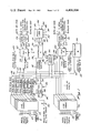
- FIG. 10 shows the structure of ring scheduling card 88 in FIG. 1.
- Ring scheduling circuitry is necessary both to accommodate the different ringing systems employed by the Bell Telephone System versus independent telephone companies, and to accommodate the fairly limited amount of power available in remote terminals for ringing telephones by limiting peak ringing signal power consumption.
- a ringing telephone requires about one watt to ring the bell. If a large number of telephones are all ringing simultaneously, the power supply may be inadequate, leading to system failure.
- the Bell System ringing scheme for party lines differs from the ringing scheme used by independent telephone companies. That is, on the Bell System party line up to four subscribers may be simultaneously attached to one line. Each telephone line is comprised of a tip line and a ring line.
- the ringing signals on any one party line can thus be directed to the proper phone being called by making the four individual telephones on the line each responsive to a different type ringing signal. That is, one phone may be made responsive to a ring signal having a first characteristic such as a 20-hertz ringing signal superimposed upon a positive 48-volt DC level on the tip line.
- a second phone may be made responsive to a ring signal having a second characteristic such as a twenty-hertz tone superimposed upon a negative 48-volt DC signal on the tip line.
- a third phone may be made responsive to a twenty-hertz ringing signal superimposed on a positive 48-volt DC signal on the ring line.
- the fourth phone may be made responsive to a twenty-hertz ringing signal superimposed on a negative 48-volt DC signal imposed upon the ring line.
- a different ringing scheme is utilized by the independent telephone companies for party lines in that the independents use different frequencies. That is, up to five phones may be simultaneously connected to a particular party line. Each phone on the line may be made responsive to a ringing signal of a different frequency, such as by band pass filtering.
- a duty cycle of one second on and four seconds off is imposed by the software on the ring generator shown in FIG. 10 for independent ringing. That is, all five telephones on a particular party line may be rung during a five-second inteval, by imposing a different frequency ringing signal on the line during each one-second interval of the five total seconds in the duty cycle. This can be understood more clearly by imagining that all five telephones connected to a particular party line were in a particular house.
- the ringer scheduling circuitry disclosed herein would generate a different frequency ringing signal during each second of the five total seconds of the duty cycle. Thus, the phones would all be ringing, but the actual ring portion of the familiar on-off ringing would not occur in more than one phone at any particular instance in time. If all five phones were lined up in a row, phone 1 would ring during the first second, phone 2 would ring during the second second, phone 3 would ring during the third second, and so on, until all five phones had rung their first ring.
- the Bell System requirements impose a different duty cycle on the ring generator for Bell System party lines.
- the software employed by the digital multiplexing system disclosed herein establishes a two-second on and a four-second off duty cycle when a switch on the CO controller card indicates the system is installed in a Bell System link.
- only one of the aforementioned four combinations of DC polarity and tip or ring selection will exist on the tip and ring pair of the party line.
- the digital multiplexed telephone system disclosed herein is not designed to ring more than one phone on a party line at any one time since as soon as that phone is picked up, the other phones on the line cannot be used because the tip and ring pair can carry only one conversation at a time.
- the ring generator serves all the line cards which are coupled to all the telephone lines in the system, during any two-second portion of the Bell System duty cycle, or during any one-second portion of the independent telephone company duty cycle, the ring generator can put out only one type of ringing signal. That is, for the Bell System-type ringing, the ring signal can only be superimposed on a +48 volt DC level or a -48 volt DC level. For independent ringing, the ring generator can generate only one frequency at a time. Because power is limited in the remote terminals, only a predetermined number of subscribers, three in the preferred embodiment, can be rung during any particular 2-second portion of the Bell System duty cycle.
- the remote terminal is programmed to determine all the subscribers who are supposed to be ringing at any particular moment in time and schedule them into groups of up to three subscribers for each two-second portion of the six-second duty cycle.
- the controller is programmed to arrange these groups such that all three subscribers' lines assigned to a particular two-second portion of the duty cycle have similar ringing conditions, i.e., each of the three telephones assigned to a particular two-second group must be voltage compatible with the other two such that all respond to a +48 volt DC on either the tip or ring line or all respond to a -48 volt DC on either the tip or ring line. Only the polarity need be compatible since the line cards receive ring codes which deterine whether the ring signal is applied to the tip or ring line.
- the remote terminal controller is programmed to organize a schedule of all the telephone lines which are ringing at the central office at a particular time.
- the RT controller then assembles groups of up to three frequency compatible subscribers on separate party lines for each one-second portion of the five-second duty cycle.
- the screening for compatibility and scheduling of individual subscriber lines for which ringing is desired into groups is done by the controller under software control.
- the central office terminal controller When the central office terminal controller detects ringing on a particular line, it sends a supervisory message to the remote terminal controller over the supervisory time slot which indicates which subscriber is being called and the particular ring code assigned to that subscriber's telephone.
- the messages are accumulated by the remote terminal controller in memory and organized into a table from which the ring scheduling is done by the ring scheduling subroutine of the program stored in the ROM in the controller.
- the controller 36 in the remote terminal after sorting, the controller 36 in the remote terminal generates address and control signals for the ring generator on its control and address bus 46. These signals include the card select signal on line 364 and the WRITE I/O signal on line 390 which enable decoder 374.
- the controller 36 then will take the results from its sort and determine for the first group and first portion of the duty cycle what frequency of ring signal is required and the polarity of D.C. voltage upon which the A.C. component is to be superimposed. The result of this decision, of course, depends upon whether the switch on the central office terminal controller indicates that Bell System ringing or independent telephone company ringing is desired.
- the controller 36 After enabling decoder 374, the controller 36 writes the proper data on its data bus to select either the positive or negative polarity for the DC voltage to be applied to the DC input of the secondary winding of the transformer. In the preferred embodiment, this code is written on bit D2 of data main bus 32. Bit D2 is coupled through buffer 366 and line 368 to the D input of flip-flop 370. Flip-flop 370 stores the polarity data from the CPU to control relay K1 372.
- Controller A, 36 in FIG. 1 loads flip-flop 370 in FIG. 10 by generating the proper address signal on address line ADR 1 and ADR 2 of address and controls bus 46 in FIG. 10.
- this address code appears at the input to decoder 374
- the output on line 376 coupled to the clock input of flip-flop 370 causes that flip-flop to be loaded.
- This causes the Q output of flip-flop 370 coupled to line 376 and inverter 378 to place relay K1 in the proper state via line 380 such that contacts 382 assume the desired polarity position.
- Contacts 382 serve to couple the negative 48-volt DC or positive 48-volt DC outputs of a DC voltage source (not shown in FIG. 10) to the DC input 384 of secondary winding 386 of transformer 388.
- Decoder 374 is enabled to set this chain of events in action when the WRITE I/O signal on line 390 goes low.
- This signal is a control signal generated by the controller which indicates, when it goes low, that data is being written onto data main bus 32.
- the card select signal on line 364 is a high level signal when the ring generation card is selected.
- inverter 392 presents a high level signal via line 394 to the input of NAND gate 396 to which it is coupled.
- NAND gate 396 drives its output line 398 low thereby enabling decoder 374 to decode the address bits on address lines ADR 1 and ADR 2.
- Buffer 366 buffers data lines 1-4 so that only one load is seen on these lines by the data outputs of the controller 36 in FIG. 1. If buffer 366 was not present, two of these four data lines would be loaded by two loads instead of one, i.e., latch 400 and flip-flops 370 and 422.
- the controller after loading the polarity data, must load data into latch 400 which will determine the proper frequency of ring signals to be generated. This loading is accomplished by enabling decoder 374 and placing the proper address code on address lines ADR 1 and ADR 2 so as to drive line 402 coupled to the clock input of latch 400 to the proper state to cause latch 400 to load the data from data main bus 32 and latch it on its output bus 404.
- the digital data latched on bus 404 causes divider 406 to divide the incoming clock signal on line 408 by a factor N, which factor is determined by the digital data comprising the control word on bus 404. For example, if the control word indicates that factor N is to be eight, the output signal from divider 406 on line 410 will be a pulse train having a frequency of 1,000 hertz where the incoming clock signal on line 408 is 8,000 hertz.
- the output signal on line 410 is coupled to the input of square wave generator 412 which converts the irregularly-shaped pulses on line 410 to a square wave on output line 414.
- Power down circuit 416 couples the output of square wave generator 412 to optical couplers 418 by line 420. Power down circuit 416 will disable the ring generator if the CPU valid signals on bus 421 indicate that both controllers 36 and 38 in the remote terminal have failed. The power down circuit can also disable the ring generator upon command of the controller 36. This is accomplished by the controller by enabling decoder 374 and writing the proper address code on address lines ADR 1 and ADR 2 so as to drive line 420 coupled to the clock input of flip-flop 422 to a state such as to cause loading of the flip-flop. The data input of this flip-flop is coupled to data bit D3 of data main bus 32 by line 482. Thus, the controller 36 can enable or disable the ring generator by setting bit D3 of the data main bus 32 either to one or zero and addressing flip-flop 422.
- Optical couplers 418 couple the square wave ring signal on line 420 to the input of push-pull drivers 424 and 426 by lines 429 and 430, respectively.
- Optical coupler 418 isolates the logic on its input side from the telephone line driving circuitry on its output side. Thus, if lightning strikes a particular telephone line and a voltage surge is coupled back along the line to optical coupler 418, there will be no direct electrical connection for this voltage surge into the CMOS logic circuitry on the input side of optical coupler 418.
- Drivers 424 and 426 are darlington pair amplifiers having outputs coupled via lines 600 and 624 to primary windings 432 and 434 of transformer 388.
- Secondary winding 386 has one end coupled to line 384 which end is designated the DC input.
- the other end is coupled to line 90 through the relay contacts of relay K2 579 and is designated the ring signal output.
- Line 384 can be coupled by relay contact 382 of relay K1 to either the -48 volt DC output or the +48 volt DC output of the DC supply (not shown).
- the ring signal on line 90 may be coupled to either the line cards coupled to the A side ring generator or the line cards coupled to the B side ring generator by K2 relay contact 579.
- cross-over relay circuit K2 578 which receives its input from bus 421.
- the cross-over relay circuit causes the ring signal for one side of the ring generator card to be crossed over and utilized by the other side of the system if the ring generator on that side fails, as indicated by the A and B CPU valid signals on bus 422.
- the ring generator also includes an alarm sense circuit 428 which senses when the ring voltage generated by the ring generator circuitry is too low and also senses when there has been a failure to generate any ring voltage at all, such as where an open circuit in the transformer 388 occurs. Sensing of an open circuit or other failure to produce a ring signal voltage is accomplished by testing the voltage level on line 90 via line 431 coupling line 90 to an input of alarm sense circuit 428. A low voltage ring signal condition is sensed by line 433 which couples alarm sense winding 435 to an input of alarm sense circuit 428. The other end of winding 434 is coupled to a negative 48-volt DC voltage source (not shown).
- Tri-state gate 436 When the controller desires to test the status of the alarm sense circuit 428, it enables tri-state gate 436 via line 438.
- Tri-state gate 436 has its input coupled via line 440 to the output of alarm sense circuit 428. The output of tri-state gate 436 is coupled to bit D1 of data main bus 32. The signals on line 440 are not coupled to the output on line 442 unless the enabling signal on line 438 is present.
- Line 438 is coupled to the output of NAND gate 444 which has its inputs coupled to the card select signal on line 364 and the READ I/O signal on line 446 through inverter 448 and line 450.
- tri-state gate 436 is enabled whenever the ring generator card is selected by line 364 and the READ I/O signal goes low, indicating that the data main bus 32 is being read by the controller.
- FIGS. 11 and 12 show a logic diagram of the ring generator card 88 in FIG. 1 when placed side by side.
- Decoder 374 will be found in the lower middle of FIG. 11.
- this chip is a MotorolaTM MC 14556 B CMOS dual, binary, one-of-four decoder/demultiplexers. Its enable input is coupled via line 398 to the output of NAND gate 396.
- This NAND gate has its input coupled via line 394 to the output of inverter 392.
- the other input of NAND gate 396 is coupled via line 452 to 1K resistor 454.
- this 1K resistor is coupled to the card select line 364.
- Line 364 is also coupled to ground through 1-meg resistor 456.
- the purpose of the network formed by resistors 456 and 454 is to hold card select line 354 firmly at ground potential during periods of inactivity on that line.
- the inputs of NAND gate 392 are coupled to 1K resistor 458.
- the other end of this resistor is coupled to the signal WRITE I/O on line 390.
- Line 390 is also coupled by resistor 460 to a positive 12-volt DC voltage source.
- the purpose of the network formed by resistors 460 and 458 is to hold line 390 firmly at a logic one state when the signal WRITE I/O is not being asserted low.
- the A input of decoder 374 is coupled by line 460 to 1-kilohm resistor 462. The other end of this resistor is coupled by line 464 to the ADR 1 address line generated by controller 36 in FIG. 1. Line 464 is also coupled to a ground potential by one-megohm resistor 466.
- the B input of decoder 374 is coupled via line 468 to one-kilohm resistor 470.
- the other end of resistor 470 is coupled to the ADR 2 line from controller 36 in FIG. 1. This line, 472, is coupled to ground potential by one-megohm resistor 474.
- the Q 0 is coupled via line 402 to the clock input of latch chips 476 and 478 of latch 400.
- these chips are MotorolaTM MC 14175 B quad-type D flip-flops.
- the D0 input of latch chip 476 is coupled to the output of buffer amplifier 486 by line 478.
- the D1 input of latch chip 476 is coupled to the output of buffer amplifier 488 by line 368.
- the D2 and D3 inputs of this latch are coupled to buffer amplifiers 490 and 492 by lines 482 and 484, respectively.
- the inputs of buffer amplifiers 486 through 492 are coupled to 1-kilohm resistors 494 through 500, respectively.
- the other sides of these 1-kilohm resistors are coupled to data bits D1 through D4 of data bus 32 from controller 36.
- Data lines D1 through D4 are respectively coupled to a +12 volt DC potential by 1-megohm resistors 502 through 508.
- 1-megohm resistors 502-508 and 1-kilohm resistors 494-500 The purpose of 1-megohm resistors 502-508 and 1-kilohm resistors 494-500 is to form individual networks on each of data lines 1-4 to hold them firmly at a logic one level when there is no activity on the data lines.
- buffer amplifiers 486-492 The purpose of buffer amplifiers 486-492 is to prevent excessive capacitive loading on data lines D2 and D3 which, if buffer amplifiers 488 and 490 were not present, would be coupled to two inputs, each representing one logic load.
- the structure of the data bus and controller is such that excessive capacitive loading on the data lines can result in slowness in data transfers or failures of the system to function properly.
- Data lines D5 through D8 are similarly connected to data inputs D0-D3 of latch chip 478 utilizing identical 1-megohm and 1-kilohm resistor networks to hold these data lines at a logic one level during periods of inactivity. No buffer amplifiers are present between these resistive networks and chip 478 because none of the data lines D5-D8 is connected to any other load other than inputs of latch chip 478.
- the Q0 through Q3 outputs of both latch chips 476 and 478 are coupled to the digital data input of divide-by-N counter 510 by bus 404.
- divide-by-N counter 510 is a MotorolaTM MC 14569 BCP CMOS high-speed programmable divide-by-N, dual, 4-bit BCD/binary counter.
- the data bits for programming the counter enter the control word input of the chip on bus 404.
- the clock signal enters the chip on line 512 from the output of buffer 514.
- the input of buffer 514 is coupled to 1-kilohm resistor 516 by line 518.
- the other end of 1-kilohm resistor 516 is coupled to an 8-kilohertz clock signal on line 520.
- Line 520 is also coupled to ground through 1-megohm resistor 522 forming a network with resistor 516 to condition the clock signal for buffer 514.
- buffer 514 The purpose of buffer 514 is to give the clock signal on line 520 better definition and amplitude with less noise and to prevent capacitive loading of the clock line 520.
- divide-by-N counter 510 is coupled via line 410 to the clock input of flip-flop 412.
- This flip-flop serves as a square wave generator to transform the pulses on line 410 into a square wave pattern of one-half the frequency line line 414.
- Line 414 couples the Q output of flip-flop 412 to one input of NOR gate 528.
- the Q output of flip-flop 412 is coupled by line 530 to the D input of the same flip-flop, thereby forming a divide-by-two circuit.
- the set and reset inputs of flip-flop 412 are coupled to ground.
- flip-flop 412 is a MotorolaTM MC 14013 BCP CMOS, dual, D-type flip-flop.
- the other input of NOR gate 528 is coupled via line 532 to the output of inverter 534. It is also coupled to one input of NOR gate 536.
- the other input of this NOR gate is coupled via line 530 to the D input and Q output of flip-flop 412.
- NOR gates 528 and 536 form power down circuit 416, shown in FIG. 10.
- the inputs of inverter 534 are coupled to the output of NOR gate 538.
- This gate has one input coupled to the Q output of latch 422 via line 540, and the other input coupled to the output of NOR gate 542 by line 544.
- Latch chip 422 serves as the on/off bit store allowing the controller 36 to power down the ring generator circuit of FIGS. 11 and 12 on command, as explained in the earlier discussion of FIG. 10.
- the D input of flip-flop 422 is coupled via line 482 to the output of amplifier buffer 490 which has its input coupled to data bit D3 of the controller data bus.
- the clock input of flip-flop 422 is coupled via line 420 to the Q1 output of decoder 374.
- the reset input of the latch chip 422 is grounded.
- flip-flop 422 is a MotorolaTM MC 14013 B CMOS dual D flip-flop. Controller 36 loads flip-flop 422 via the ADR 1 and 2 lines, the card select line 364 and the WRITE I/O signal on line 390.
- the controller can load a logic 1 or 0 via bit D3 of its data bus thereby setting or resetting the Q output on line 540.
- This signal ripples through NOR gate 538, inverter 534, and power down NOR gate 536 to ultimately emerge on line 546 coupled to the input of inverter 548.
- inverter 548 is a MotorolaTM MC 1416 P open collector-type inverter.
- open collector inverter 548 is coupled via line 554 to the negative end of the light emitting diode in optical coupler 558.
- the positive end of the light emitting diode is coupled through resistor 560 to a positive 12-volt DC supply.
- An identical circuit is coupled to the output of open collector inverter 552 for driving the LED of optical coupler 568 in FIG. 12.
- the controller can control these signals at the input of open collector inverters 548 and 552. In one input condition, these inverters will sink current to ground through their outputs. In the other condition, they will refuse to sink current.
- the controller has complete control over the current flowing through the light emitting diodes in optical couplers 558 and 568 and thus it has control over the base current of the input transistors of drivers 424 and 426.
- the lowered light emission from the LEDs causes the transistors in the optical couplers to have a lower emitter current. The controller can therefore shut down current flowing in drivers 424 and 426 to save power.
- This shut-down feature is also actuated automatically in the eventuality that both controllers fail.
- the A CPU VALID and B CPU VALID signals on bus 421 in FIG. 12 will assume a logic state which causes the output signal of NOR gate 542 on line 544 to ripple through NOR gate 538, inverter 534, and NOR gates 536 and 528 so as to cause open collector inverters 548 and 552 to shut down the light emitting diodes in the optical couplers.
- the inputs of NOR gate 542 are coupled to the A CPU VALID and B CPU VALID signals through 10K resistors 570 and 572. Both the A CPU and the B CPU VALID signals are coupled to ground through two megohm resistors 574 and 576. These resistors insure that the A CPU and B CPU VALID lines are firmly held at ground potential during periods of inactivity on these lines.
- the digital multiplex system disclosed herein utilizes dual ring generators for reliability purposes. Should one ring generator fail, a cross-over circuit will detect the signal indicating that a controller has detected a failure in one of the ring generating cards. This cross-over circuit will cause the still-operating ring generator to switch over to supply a ring signal to the side which has failed.
- This cross-over circuitry is comprised of inverter 574, open collector inverter 576, and relay K2 578. The inputs of inverter 574 are coupled to the A CPU VALID signal, but, on the other side, the inputs would be coupled to the B CPU VALID signal.
- inverter 574 is coupled to the input of open collector inverter 576 which has its output coupled to the coil of relay K2 578.
- the other end of the coil of K2 is coupled to the positive 12-volt DC supply.
- the inverter output goes to logic zero and sinks current through the relay coil of K2, thereby energizing the relay. This causes relay contacts 428 in the upper-center portion of FIG. 12 to operate so as to connect the ring signal on line 90 to the cross-over line 582 coupled to the other ring generator as opposed to the normal ring signal line 90.
- Flip-flop 370 in FIG. 11 is the plus or minus polarity bit memory. Its data input is coupled by line 368 to the output of buffer amplifier 488 which in turn is coupled to the D2 bit of data main bus 32. The clock input of this chip is coupled via line 376 to the Q2 output of decoder 374. The set and reset inputs of flip-flop 370 are grounded. In the preferred embodiment, this flip-flop is a MotorolaTM MC 14013 BCP. Controller 36 in FIG. 1 can control the polarity of the DC voltage applied to the DC input 384 of secondary winding 386 of the transformer 388 in FIG. 12.
- Controller 36 exercises this control by setting or resetting bit D2 of its data bus after addressing latch 370 via the ADR 1 and 2 lines and the ring generator card select line 364 in address and control bus 46.
- the Q output of flip-flop 370 is coupled to the input of open circuit inverter 378 by line 376.
- the output of this inverter is coupled by line 380 to the coil of relay K1 372.
- the other end of this coil is connected to a positive 12-volt DC supply.
- controller 36 can control the energization state of relay K1 through bit D2 of its data bus, flip-flop 370, and inverter 378.
- Darlington pair 424 is conventional and apparent to those skilled in the art. Likewise, for darlington pair 426.
- Capacitors 584 and 586 function in a noise suppression capacity.
- the transistor in optical coupler 568 has its base coupled to a 1-megohm resistor 588, the other end of which is coupled to a -48 volt DC supply.
- the collector of this transistor is grounded, and the emitter is coupled to an 8.2-kilohm resistor 590.
- the other end of this resistor is coupled to the base of transistor 592.
- the base of transistor 592 is also coupled by a 10-kilohm resistor 594 to the emitter of transistor 592.
- the emitter of transistor 592 is coupled to the base of transistor 596.
- the collector of transistor 592 is coupled to the collector of transistor 596 and to the negative end of diode 598 and to one end of primary winding 432 by line 600.
- the base of transistor 596 is coupled by 150-ohm resistor 602 to the emitter of transistor 596.
- the emitter of transistor 596 is coupled to the positive end of diode 598 and to the ungrounded end of capacitor 584 by line 604.
- Line 604 is also coupled to the emitter of transistor 606.
- the emitter of transistor 606 is coupled to the base of transistor 606 by 10K resistor 610.
- the base of transistor 606 is also coupled through 8.2K resistor 612 to the emitter of the transistor in optical coupler 558 by line 614.
- the base of the transistor in optical coupler 558 is coupled through 1-megohm resistor 616 to a -48 volt DC supply.
- the collector of the transistor in optical coupler 558 is grounded.
- the emitter of transmitter 606 is also coupled to the emitter of transistor 608 by 150-ohm resistor 618.
- the emitter of transistor 606 is also coupled to the base of transistor 608 by line 620.
- the collector of transistor 608 is coupled to the collector of transistor 606 and to the negative end of diode 622 and to one end of primary winding 434 by line 624.
- the emitter of transistor 608 is also coupled via 10-ohm resistor 626 to the ungrounded end of capacitor 586.
- the two ends of primary windings 432 and 434, not already mentioned, are coupled to ground by line 628.
- the ends of capacitors 584 and 586 not already mentioned are coupled to ground via line 628.
- the -48 volt DC supply on line 582 is coupled by 10-ohm resistor 628 to 0.047-microfarad capacitor 630. Relay contacts 382 are bypassed by 0.047-microfarad capacitor 630 and 20-ohm resistor 632 for spark suppression purposes.
- the positive 48-volt DC supply coupled to line 584 is also coupled to 0.047-microfarad capacitor 634 and 20-ohm resistor 636 which bypass the second set of ganged contacts 382 for spark suppression purposes.
- Line 431 coupling the output of secondary winding 386 to the input of alarm sensor 428 provides the information necessary for the alarm sensor 428 to determine whether there has been an open circuit in the transformer or a failure to generate any ring signal voltage on line 90.
- Line 431 is coupled to a 47K resistor 642 which has its opposite end coupled to the negative end of a light emitting diode in optical coupler 644. The positive end of the light emitting diode is grounded. Diode 646 bypasses the LED for protection purposes having its positive end coupled to the negative end of the LED and vice versa.
- the base of the transistor in optical coupler 644 is left open. The collector of this transistor is coupled to the 12-volt supply by 51K resistor 650.
- the collector is also coupled to the collector of transistor 652 and the input of tri-state gate 654 by line 656.
- the emitter of the transistor in optical coupler 644 is coupled to the base of transistor 652 by line 658.
- the emitter of transistor 652 is coupled to ground through line 662.
- the output of tri-state gate 654 is coupled to bit D2 of data main bus 32 by line 664.
- Line 433 couples secondary winding 435 of transformer 388 to the positive end of diode 666.
- the other end of secondary winding 435 is coupled to the -48 volt DC supply.
- the negative end of diode 666 is coupled through 10K resistor 668 to the positive end of electrolitic 10-microfarad capacitor 670. The other end of this capacitor is coupled to the negative 48-volt supply.
- Diode 666, resistor 668, and capacitor 670 form a detector circuit which detects the signal voltage appearing on secondary winding 435.
- the output voltage at node 672 is indicative of the amplitude of the ring signal waveform generated by drivers 424 and 426. This signal voltage is coupled by line 674 to the negative input of comparator 676.
- Node 672 is also coupled to the 48-volt negative DC supply by 100K resistor 678.
- the positive input of comparator 676 is coupled via line 680 to 330K resistor 682.
- Line 680 is also coupled to the negative 48-volt supply through 9.53K resistor 684.
- Line 680 is also coupled to 16.9K resistor 686, the other end of which is coupled to one end of 0.1-microfarad capacitor 688. The other end of this capacitor is coupled to the negative 48-volt DC supply.
- Line 690 couples the node between resistor 686 and the first end of capacitor 688, and the positive end of zener diode 692 to ground through 2.7K resistor 694. The other end of zener diode 692 is coupled to the -48 volt supply.
- Line 690 is also coupled to one end of a 0.1-microfarad capacitor 696 and to pin 7 of comparator 676.
- comparator 676 is a generic 741 type manufactured by several sources.
- the other end of capacitor 696 is coupled to the -48 volt DC supply and to pin 4 of comparator 676.
- the output of comparator 676 is coupled to 2.7K resistor 698 and to the other end of 330K resistor 682 via line 700.
- the other end of resistor 698 is coupled to the positive end of the light emitting diode in optical coupler 702.
- the negative end of this light emitting diode is coupled to the negative 48-volt DC supply.
- the transistor of this optical coupler 702 has its collector coupled to the positive 12-volt DC supply and its emitter coupled via line 440 to the input of tri-state gate 436.
- the emitter of the transistor is also coupled through a 100K resistor 706 to ground.
- the controller When the controller wishes to read alarm bit A, it selects the ring generator and card using the CARD SELECT signal on line 364 and enters a read cycle. This causes the READ I/O on line 446 to go low. This in turn causes inverter 448 to raise its output on line 450 which causes NAND gate 444 to lower its output line 438 thereby enabling tri-state gate 436 and coupling line 440 to bit D1 of the controller data bus via line 442.
- the voltage on node 672 is compared by comparator 676 against a reference voltage established on line 680 by the resistor network coupled thereto. If the voltage peaks on node 672 are reaching above the reference voltage, comparator 676 outputs signals on line 700 which are optically coupled by coupler 702 to the input of tri-state gate 436.
- optical coupler 644 in FIG. 12 and transistor 652 in conjunction with alarm bit B will be apparent to those skilled in the art.
- FIGS. 13a and 13b show a logic diagram of the re-frame buffer 178.
- Line receiver chip 800 in FIG. 13b receives the NRZ, i.e., unipolar, data on line 58, from span line terminating card 54 in FIG. 1.
- Line receiver chip 800 also receives a clock input signal on line 62 also from span terminating card 54 in FIG. 1. This clock signal has a frequency of 1.544 megahertz, and is synchronized with the occurrence of each bit in the serial bit stream on line 58.
- line receiver chip 800 is a RockwellTM R8060.
- the line receiver chip converts the serial data at its input to parallel output data on lines CDB 1-8. It also generates a channel clock signal on line 802 which marks each time slot. That is, the channel clock signal on line 802 goes high once for each time slot.
- Line 802 is coupled to the input of inverter 804 which has its output coupled via line 182 to the CP or count input of counter chip 806.
- the signals on line 182 serve to increment counter 806 such that the output data on bus 176 indicate the binary number representing the number of the time slot which is currently being received by line receiver 800.
- Line receiver 800 also generates a frame alarm signal on line 812 which goes high when there is a loss of frame synchronization with the input data. That is, when line receiver 800 fails a predetermined number of times to detect the frame bit in the input data at the end of all twenty-four time slots in a frame, it will set the frame alarm signal on line 812.
- Line receiver 800 also generates a channel synchronization signal on line 814 and a write inhibit signal on line 816.
- the channel synchronization signal is a low-going pulse which occurs at the end of each frame.
- the write inhibit signal indicates when it is impermissible to write new data to the input of line receiver 800. This signal goes high for a portion of each time slot.
- the write inhibit signal on line 816 is coupled to the input of AND gate 818, the other input of which is coupled via line 820 to the output of inverter 822.
- This inverter has its input coupled to the channel synchronization signal on line 814.
- the output of AND gate 818 is coupled to the reset input of counter 806 by line 824.
- the output of AND gate 818 on line 824 goes high at the end of every frame for a portion of a time slot. This resets time slot counter 806 so that it may begin counting the time slots of the next frame.
- Line receiver chip 800 also generates a carrier loss alarm on line 177 which is coupled to controller 36 in FIG. 1 through the status register in the multiplexer, as shown in FIG. 5, to indicate that no serial data is being received from the span line.
- time slot counter 806 on bus 176 are coupled to the data inputs of FIFO buffer chips 828 and 830.
- the data outputs of line receiver chip 800 are coupled to the data inputs of FIFO buffer chips 832 and 834 by bus 176.
- Another layer of FIFO buffer memory is provided by FIFO buffer chips 836, 838, 840 and 842.
- FIFO buffer chips 828 through 842 are RCATM 40105B chips in the preferred embodiment. These chips work as follows. Data presented at data inputs D0-D3 is loaded into the first level of the stack when the shift input signal, marked SI, goes high. Each time the shift input signal goes high, the data present at a D0, D1, D2, and D3 input is loaded into the next level down in the stack. The DIR output signal indicates by one binary state that the FIFO memory chip is ready to accept new data. The other binary state indicates that the FIFO memory chip is not ready to store new data. The master reset input, marked MR, clears the entire stack when it is driven to a high level.
- Each of FIFO memory chips 828-842 contains a stack of sixteen 4-bit words.
- the outputs of the first level of the stack from FIFO chips 828, 830, 832, and 834 on bus 844 are coupled to the input bits D0, D1, D2, and D3 of the second level of the FIFO stack comprised of chips 836, 838, 840, and 842. Therefore, the overall re-frame FIFO buffer is thirty-two levels deep and sixteen bits wide. This comprises approximately a frame-and-a-half of serial input data.
- the shift-out input, marked SO causes, when it is driven high, the next level down in the stack to be moved to the output bits Q0-Q3.
- the purpose of the FIFO stack is to hold the 8-bit parallel digital data for each time slot together with its time slot count until this time slot count comes up again on the internal data bus of the multiplexer.
- the re-frame buffer then releases it to the internal PCM data bus 180 for transfer to various locations in the multiplexer. This is accomplished as follows. During time slot zero, the serial data coming into line receiver chip 800 is converted to parallel data on lines CDB1 through CDB8 and coupled to the data inputs of FIFO chips 832 and 834 by bus 176. At the same time, the binary information on output bits Q1-Q5 of time slot counter 806 representing time slot zero is coupled via bus 176 to the data input of FIFO buffers 828 and 830.
- This data is loaded into the first level of the stack and appears on data outputs Q0 through Q3 of FIFO buffer chips 828, 830, 832, and 834.
- the appearance of this data at the outputs is marked by the transition of the DOR signal of FIFO buffers 828-834 from a low to a high level. These transitions are coupled to the shift in input pins of FIFO buffers 836, 838, 840, and 842 by lines 845, 846, 848, and 850, respectively.
- This causes the data at the outputs of buffer chips 828, 830, 832, and 834 to be loaded into the first level of the stack comprised of buffers 836-842 via bus 844.
- This data is then presented at outputs Q0-Q3 of buffer chips 836, 838, 840, and 842 which appearance is marked by a low to high transition of the DOR outputs of these buffer chips.
- buffer chips 836-842 are ready to receive another data word, the DIR signal output goes high. These transitions are coupled to the shift out inputs of buffers 828-834 via lines 852, 854, 856, and 858, respectively. This low to high transition causes buffers 828 through 834 to shift the next level down in the stack to their outputs. Prior to that time, the next level down in the stack comprised of buffers 828-834 had been filled by the parallel data of time slot one. This data was loaded at the end of time slot one when the channel clock signal on line 802 from line receiver 800 changed state so as to indicate that the data on lines CDB 1-8 was then the data for time slot one.
- This change of state of the channel clock signal was coupled through inverter 804 to time slot counter 806 incrementing it to indicate that time slot one was then being received.
- This change of state on line 182 was also coupled to the shift-in input, SI, of buffer chips 828-834. This caused these chips to load the data at their inputs into the next empty level of the stack. This data was then transferred to the outputs of buffers 836-842 in a similar fashion as was the data for time slot zero.
- the FIFO stack acts as an elastic buffer to temporarily store incoming data until its time slot, as determined by the internal time slot counter in control timing 184 in FIG. 5, comes up whereupon it is transferred via the internal PCM data bus to wherever it happens to be going as determined by controller 36. In this fashion, any variable delays in transmission over the span line will not cause multiplexer 42 to get out of synchronization with the multiplexer in the terminal at the other end of the span line.
- loading of the data from FIFO buffers 840 and 842 onto internal PCM data bus 180 is accomplished by comparing the stored time slot count at the top of the FIFO stack in chips 836 and 838 with the time slot count as determined by control timing 184 in FIG. 5. This comparison is done by comparator 860.
- the B side of this comparator, inputs B0, B1, B2, and B3, are coupled via bus 210 to the outputs of the time slot counter in control timing 184, i.e., bits TC4, TC8, TC16, and TC32.
- Resistors 862, 864, 866, and 868 are all 10K resistors and couple these bits to a positive level supply to hold them affirmatively at a logic one level unless they are being asserted at a logic zero level by the time slot counter.
- comparator 860 is a MotorolaTM MC 14585 BCP.
- the four outputs from FIFO buffer 838 are coupled to the A side inputs of comparator 860, bits A0-A3, by bus 870.
- the A Greater Than B and VDD inputs are coupled to the positive 5-volt supply by line 872.
- the A Less Than B and VSS inputs are coupled to ground by line 874.
- the A Equals B input is coupled to the output of AND gate 876 by line 878. In this configuration, when line 878 is a logic one, the A Equals B output on line 880 will be a logic one if A0 equals B0, A1 equals B1, A2 equals B2, and A3 equals B3.
- Line 880 is coupled to one input of exclusive-OR gate 882 which has its other input coupled by line 884 to the +5 volts supply.
- exclusive-OR gate 882 is functioning as an inverter and, indeed, a simple inverter would serve the purpose.
- the output of inverter 882 is coupled via line 884 to the tri-state inputs, TS, of FIFO buffers 840 and 842.
- Comparator 860 is enabled through the following network.
- One input of AND gate 876 is coupled by line 886 to the output of exclusive-OR gate 888.
- One input of this exclusive-OR gate is coupled by line 890 to the TC2 bit from the time slot counter in control timing 184 of FIG. 5.
- Line 890 is also coupled via 10K resistor 892 to the +5 volts supply to hold this line firmly at a logic one when TC2 is not being affirmatively asserted low.
- the other input of exclusive-OR gate 888 is coupled via line 894 to the output of inverter 896. This inverter has its input coupled via line 898 to the Q3 output of FIFO buffer 836.
- the other input of AND gate 876 is coupled via line 900 to the output of AND gate 902.
- This AND gate has its inputs coupled to the data output ready outputs, DOR, of FIFO buffers 836, 838, 840, and 842 via bus 904. Therefore, if any of buffers 836-842 do not have data ready on their outputs, one of the lines in bus 904 will be at a logic zero level. This will cause line 900 to be at a logic zero level. Thus, line 900 will be a logic one only if all four FIFO buffers 836-842 have data ready at their output.
- Exclusive-OR gate 888 in the configuration shown in FIG. 13A acts as a two-bit comparator comparing the Q3 output bit of FIFO buffer 836 to the TC2 output bit from the time slot counter in control timing 184 of FIG. 5.
- the Q3 bit if FIFO buffer 836 holds the data which was loaded into the D3 input of FIFO buffer 828 from the Q1 output of time slot counter 806 via bus 176.
- exclusive-OR gate 888 By inverting the Q3 bit in inverter 896, exclusive-OR gate 888 generates a logic one on its output line 886 when the signals on line 890 and Q3 from FIFO buffer 836 are at the same logic level.
- line 878 is raised to a logic one level, thereby enabling comparator 860 which makes the comparison. If the time slot counter bits TC4, TC8, TC16, and TC32 are the same as the output bits Q0-Q3 of FIFO buffer 838, a logic one appears at the A Equals B output on line 880. This is inverted in inverter 882 and coupled via line 884 to the tri-state inputs of FIFO buffers 840 and 842. The logic zero on line 884 enables FIFO buffers 840 and 842 to drive the internal PCM data bus 180.
- the shift-out inputs of FIFO buffers 836 through 842 are coupled via line 902 to the output of inverter 904.
- This inverter has its input coupled to the output of AND gate 906 by line 908.
- This AND gate has one input coupled to the dump FIFO signal on line 910 and the other input coupled via line 912 to the Q output of latch 914.
- Line 910 is also coupled via 10K resistor 916 to the positive five-volt supply such that line 910 will be affirmatively held at logic one when the dump FIFO signal is not being asserted low.
- latch 914 The reset input of latch 914 is grounded and the clock input is coupled to the LOAD RB signal on line 918.
- the D input of latch 914 is coupled via line 880 to the A Equals B output of comparator 860.
- Latch 914 also has its set input and pin 7 coupled to ground. In the preferred embodiment, this latch is a generic type 4013B flip-flop. Likewise, time slot counter 806 is a generic 4024B.
- the signal LOAD RB is a positive going pulse that occurs during every other write cycle of the signal R/W generated by control timing 184 in FIG. 5. It should be noted at this point that control timing 184 is coupled as needed to all the blocks shown in FIG. 5 with various signals from the PCM bus clock and timing bus 146.
- the signal R/W controls the read and write cycle for each MUX internal time slot on internal PCM data bus 180.
- the signal DMP FIFO is a positive going pulse during every other read cycle of the signal R/W from control timimg 184.
- the signal on line 910 is a logic one during every other read cycle of the multiplexer and the signal on line 918 is a logic one during every other write cycle of the multiplexer.
- the circuitry for generating the signals dump FIFO and load RB is not shown in FIG. 13 but will be apparent to those skilled in the art.
- multiplexers 42 and 44 each have two internal time slots for every one time slot on the span line, and because each internal multiplexer time slot is comprised of one read cycle and one write cycle, the signal LOAD RB on line 918 will load latch 914 only once during ever time slot of the span line. Because its data input is coupled via line 880 to the A Equals B output of comparator 860, latch 914 will load a logic one only when the time slot of the span currently being processed by the multiplexers, as indicated by the TC2, 4, 8, 16, and 32 bits on the B input of comparator 860 equals the time slot count indicated at the output of FIFO buffers 836 and 838. When latch 914 loads a logic one, its Q output on line 912 will go to a logic one level.
- line 908 at the output of AND gate 906 will go to a logic one level only when the time slot counts are equal and the read cycle of an internal MUX time slot is occurring.
- the signal on line 908 is inverted in inverter 904 and applied via line 902 to the shift-out inputs of buffers 836 through 842. This will cause the next words down in the stack to be shifted to the outputs and held there.
- the data previously on these outputs will have been read from the internal PCM data bus 180 during the previous internal MUX read cycle with the same time slot on the span line.
- the master reset of FIFO buffer 828 through 842 are all coupled via line 922 to the Q output of latch 924.
- the clock input of latch 924 is coupled via line 182 to the output of inverter 804 which has its input coupled to the channel clock signal, CHCLK, on line 802.
- the data input of latch 924 is coupled via line 926 to the output of AND gate 928.
- This AND gate has one input coupled to the signal CARR. LOSS, and the other input coupled via line 930 to the output of AND gate 932.
- the inputs of AND gate 932 are coupled to the data input ready outputs of FIFO buffers 828 through 834 via bus 934.
- the output of AND gate 932 on line 930 thus will be a one only when all of FIFO buffers 828-834 are ready to receive additional data on their data inputs D0-D3. Assuming that no loss of carrier is indicated by the signal CALRM on line 177 from line receiver 800, the signal CARR. LOSS on line 936 will always be a logic one. Therefore, as long as the signals on bus 934 all indicate readiness to receive additional data at the end of each time slot, as marked by the signal on line 182, latch 824 will continue to load logic ones via line 926.
- any one of FIFO buffer chips 928-834 fills up all sixteen of its 4-bit words, one of the signals on bus 934 will go to a logic zero level and be in that state at the end of a time slot.
- line 930 goes to a logic zero level causing line 926 to go to a logic zero level, thereby loading a zero into latch 924 at the end of one time slot.
- This sets the Q output on line 922 at a logic one level which signals the master resets of FIFO buffer chips 828-842 to clear the entire contents of the FIFO buffer.
- the logic one level on line 922 also constitutes the signal FRAME LOSS which is coupled to the controllers indicating that a frame of data has been lost due to overflow of the FIFO buffer.
Abstract
Description
APPENDIX I __________________________________________________________________________ RTController __________________________________________________________________________ C3 64 D4 98 1B B2 4.0. 64 4.0. 7F 7F 53 E7E7 D2 A9 24BF EA 84 .0.8 D.0. 51 F6 E5 F4 E1 F4 F6 3F .0.D 9D B7 .0.2 .0.C 1A 55 D.0. 1E AC 3F FA FB 37 7E F7FF 2D C3 44D4 48 9D 75 41 79 3B 87 2D 1A A8 8E ED E6 AF 1.0. 4B .0.D 79 .0.D CB 1F AF 53 FE CB FB 65 AD 37 51 18 D2 11 DA DF CB 73 E6 AA 6B 61 .0.D 57 AF A3 5.0. 91 23 8.0. .0.A C6 C3 .0.B D4 8E 7F A4 43 1E 4B FD 2.0. 76E9 48 21E8 32FA 54 24 .0.5 67 D4 EF C6 89F3 31 .0..0. 48 3E .0.1D3 C8 32 .0.D 4.0. 21 FF FF .0.1 FF FF CD .0.9 .0.5DD 21 .0..0. .0..0. .0.1 .0..0. 28D9 21 FF FF D3 D8 11 21 1.0.DD 46 .0..0.DD 23 .0.E .0.8 29 1F A8 E6 8.0. 28 .0.6 7C AA 677D AB 6F 78 .0.7 47 .0.D 2.0. ED D9 .0.B 78 B1 D9 2.0. DA 7D B4 CA D7 .0..0. 21 .0.7 .0..0. .0.6 .0.2 .0.E .0.1 CD .0.9 .0.5 C3 D4 .0..0. 21 .0..0. 4.0. .0.6 .0.3 D3 D8 7.0. .0.4 2.0. .0.2 .0.6 .0.3 237C FE 48 2.0.F2 26 4.0. .0.6 .0.3 D3 D8 7E B8 C2 27 .0.1 .0.4 2.0. .0.2 .0.6 .0.3 237C FE 48 2.0.EE 26 4.0. D3 D8 7E 2F 77 237C FE 48 2.0.F5 26 4.0. .0.6 .0.3 D3 D8 7E 2F B8 C2 27 .0.1 .0.4 2.0. .0. 2 .0.6 .0.3 237C FE 48 2.0.ED C3 34 .0.1 21 .0.7 .0..0. .0.6 .0.2 .0.E .0..0. CD .0.9 .0.5C3 31 .0.1 CD A8 .0.1 CD 49 .0.1 CD D3 .0.2 CD 87 .0.3 CD 35 .0.4 CD BD .0.3C3 26 .0.5DB E1 32 .0.B 4.0. DB E.0. 32 .0.A 4.0. CB .0.7 CB .0.7 E6 .0.3 32 .0..0. 4.0. 3A .0.A 4.0. 1F 1F 1F 1F E6 .0.3 32 BF 4.0. 3A .0.B 4.0. CB 4F 2.0. .0.4 3E .0.2 18 .0.2 3E .0.8 32 .0.E 4.0. 3A .0.A 4.0. 21 .0.9 .0..0. .0.1 34 .0..0.CB 4F 28 .0.6 21 34 .0..0. .0.1 .0.8 .0.2 22 5D 45 ED 43 5F 45 ED 43 55 45 ED 43 57 45 3E .0..0. 32 59 45 32 5B 45 3E .0.A 32 .0.9 4.0.C9 16 .0..0. 21 .0..0. 4.0. .0.1 FC .0.7 72 23 .0.B 78 B1 2.0. F9 3E .0.4 32 .0.6 4.0.3E 14 32 66 45 D3 D8 .0.1 32 .0..0. 21 21 4.0. CD FE .0.4 21 23 4.0. 22 21 4.0. .0.1 26 .0..0. 21 53 4.0. CD FE .0.4 21 55 4.0. 22 53 4.0. .0.1 32 .0..0. 21 79 4.0. CD FE .0.43E 42 32 81 4.0. 32 8B 4.0. 32 95 4.0. 32 9F 4.0. 32 A9 4.0. 3E .0..0. 32 82 4.0. 32 8C 4.0. 32 96 4.0. 32 A.0. 4.0. 32 AA 4.0. .0.1 12 .0..0. 21 AB 4.0. CD FE .0.4 21 .0..0. .0..0. 22 BD 4.0. 3E .0.1 32 C.0. 4.0. 32 C5 4.0. 3E .0..0. 32 C6 4.0. 3E .0.2 32 C7 4.0. 21 79 4.0. 22 C3 4.0. 3E FF .0.E .0.F .0.6 8.0. 21 C9 4.0. 11 .0.4 .0..0. 71 23 77 19 1.0. FA D3 D8 .0.1 BC .0..0. 21 49 43 CD FE .0.4 21 4D 43 22 4B 43 21 .0..0. .0..0. 22 49 43 21 .0.5 44 22 43 44 21 24 44 22 45 44 .0.1 B7 .0..0. 21 94 44 3E .0.5 77 23 .0.B 79 B.0. C2 6E .0.2 21 96 44 22 94 44 3EFA 32 4F 45 3E .0.1 32 4E 45 21 .0.1 .0.1 22 2C 45 22 2E 45 3E .0.52F 32 3.0. 45 21 31 45 .0.6 19 AF 57 15 72 82 23 1.0. FA 2F 77 DB F8 E6 1.0. .0.F 32 4B 45 D3 D8 3E .0.1 32 18 4.0.3E 14 32 17 4.0. 21 .0.F 4.0. 22 1B 4.0. 21 431D 22 1D 4.0. 214A 44 22 48 44 .0.1 36 .0..0. CD FE .0.4 C9 D3 D8 3E .0..0.2F D3 883E 18 32 .0.7 4.0.2F D3 88 3E .0..0. 2F D3 8B CD .0.5 14 3E BC 2F D3 8A 3E BF 2F D3 89 .0.62E CD 13 .0.3 CD .0.5 14 3E BF 2F D3 8A 3E 7F 2F D3 89 .0.62F CD 13 .0.3 21 .0.2 4.0.CB E6 C3 24 .0.3 D3 D8 C5 CD .0.5 14C1 78 2F D3 8B .0.5 .0.5F2 13 .0.3 C9 3E FE 2F D3 8.0. CD .0.5 14 3E BC 2F D3 8A 3E C.0. 2F D3 89 3E .0..0. 2F D3 8B 3E .0.1 32 .0.8 4.0. 2F D3 8.0. D3 8.0. D3 D8 3E .0..0. 2F D3 9E 3E .0.4 2F D3 91 3E .0..0.2F D3 923E 31 D3 C8 3E 35 32 .0.D 4.0. D3 C8 DB C.0. CB 47 28 18 214A 44 .0.6 .0.F .0.E C.0. ED B3 DB C.0. CB 47 28 .0.E 7E ED 79 DB C.0. CB 47 28 .0.5 21 11 4.0. CB F6 DB E8 C9 ED 5E 3E .0..0. ED 47 3E 4.0. .0.E D.0. ED 79 3E C7 ED 79 3E .0.1 ED 79 .0.E D1 3E A7 ED 79 3E 4E ED 79 .0.E D2 3E A7 ED 79 3E C3 ED 79 .0.E D3 3E C7 ED 79 3E .0.1 ED 79 FBD3 D8 C9 21 12 4.0. CB C6 DB F8 CB 67 28 .0.8 CD 57 .0.7 CB CE C3 DD .0.3 3A .0.A 4.0. CB 47 CA DD .0.3 CB D6 CD 5B .0.7 3A 67 45 CB 5F CA 19 .0.4 .0.6 .0.5CD 421F 21 12 4.0. CB C6 CD 57 .0.7 CD 57 .0.7 CD 57 .0.7 21 8.0. 44CB 46 C2 19 .0.4CB 4E C2 12 .0.4 21 .0.2 .0..0. .0.6 .0.2 .0.E .0..0. CD .0.9 .0.5 C3 .0.F .0.4 21 .0.2 4.0.CB FE 18 11 F3 3E .0.4 32 .0.D 4.0. D3 C8 CD EE .0.4 21 12 4.0.CB 86 FB 3E .0.32F D3 9E 21 .0.1 4.0.CB C6 C9 21 15 4.0.CB FE 16 .0.2 3A .0.8 4.0. CB D7 2F D3 8.0.2F CB 97 2F D3 8.0. D3 8.0. DB 8.0.2F CB 4F 28 .0.5 .0.E .0.1 C3 E1 .0.4 21 2C 45 .0.6 2.0. .0.E 82 ED B3 DB 8.0. 2F CB 4F 2.0. .0.8 15 2.0. D1 .0.E .0.2 C3 E1 .0.4 CD .0.5 14 3E BD 2F D3 8A 3E 4.0. F6 2F 2F D3 89 3E 2E 2F D3 8B CD 5B .0.7 21 .0.1 4.0. CB D6 CD .0.5 14 3E BE 2F D3 8A 3E C.0. F6 2F 2F D3 89 3E 2F 2F D3 8B .0.1 .0..0. .0.13A 15 4.0.CB 7F 28 .0.A .0.B 78 B1 2.0. F4 .0.E .0.3 C3 E1 .0.4 21 .0.1 4.0.CB 96 DC .0.5 14 3E BD 2F D3 8A 3E C.0. F6 2E 2F D3 89 3E 2E 2F D3 8B 3A .0.F 4.0. CB 57 2.0. .0.1C9 F3 21 .0.2 .0..0. .0.1 .0..0. .0.5 CD .0.9 .0.5 18F4 F3 21 .0.2 .0..0. .0.6 .0.3 CD .0.9 .0.5 C3 E1 .0.4 C9 D3 D8 .0.E 7F 3E .0..0. 2F ED 79 .0.D F2 F5 .0.4 D3 D8 C9 3E FF 77 23 .0.B A.0. B1 C2 FE .0.4 C9 3A .0.D 4.0. CB F7 D3 C8 7C 2F D3 9A 7D2F D3 9B 78 2F D3 9C 79 2F D3 9D 3A .0.D 4.0. D3 C8 C9 CD 57 .0.7 21 .0.2 4.0. CB DE CD .0.4 .0.7CD 62 .0.6 CD D7 .0.6 CD 4B .0.5 CD 7B .0.F CD 1A .0.F CD 19 1D CD B.0.1D CD 24 .0.7 18 E3 3A .0.3 4.0. CD 3.0. .0.B DB 99 CB 7F C8 FD CB .0..0. 46 CA 49 .0.6 FD CB .0.1 6E C2 49 .0.6 FD CB .0.4 7E C2 49 .0.6 21 15 4.0.CB 9E 21 14 4.0.CB 86 FD CB .0.4 EE F3 CD .0.5 143A 13 4.0. CB 57 C2 A.0. .0.5 3A .0.3 4.0. 2F D3 8A 3E .0..0. 2F D3 89 3E .0.3 2F D3 8B CD .0.5 143A 13 4.0. CB 57 CA A4 .0.5 FB C3 4.0. .0.6 3E FF 2F D3 8A 3E .0..0. 2F D3 89 3E .0.1 2F D3 8B FB 3A .0.3 4.0. 4F 3E .0.2 2F ED 79 3E .0.3 2F D3 9F CD 57 .0.7 DB 99 2F CB 47 CA E6 .0.5 FD CB .0.4 76 CA 4.0. .0.6 .0.6 1.0. 3E .0.8CD 44 14 FD CB .0.4B6 21 19 4.0. 35 C3 4.0. .0.6 3E .0.1 2F D3 9F CD 5B .0.7 DB 99 2F CB 47 C2 FE .0.5 21 14 4.0. CB C6 C3 4.0. .0.6 3E 43 2F D3 9F CD 5B .0.7 DB 99 2F CB 47C2 16 .0.6 21 15 4.0. CB DE C3 4.0. .0.6 FD CB .0..0. 46 CA 4.0. .0.6 FD CB .0.1 6E C2 4.0. .0.6 FD CB .0.4 7E C2 49 .0.6 FD CB .0.4 76 2.0. .0.F .0.6 2.0. 3E .0.8CD 44 14 FD CB .0.4F6 21 19 4.0. 34 3A .0.3 4.0. 4F 3E .0..0. 2F ED 79 FD CB .0.4 AE 3E .0..0. 32 .0.4 4.0. 3A .0.3 4.0.3C 32 .0.3 4.0. FE 8.0. C.0. 3E .0..0. 32 .0. 3 4.0.C9 21 .0.2 4.0. CB 6E C8 CB AE F3 3E 8.0. 21 C8 4.0. 36 .0..0. 23 36 .0.F 23 36FF 23 36 .0..0. 23 36 .0..0. 23 3D C2 7.0. .0.6 FB F3 .0.1 BC .0..0. 21 49 43 CD FE .0.4 21 4D 43 22 4B 43 21 .0..0. .0..0. 22 49 43FB 21 .0.1 4.0.CB FE 21 13 4.0.CB BE 21 .0.1 4.0.CB A6 21 .0.F 4.0. 16 .0..0. 3E .0.8CD 9C 1D 21 1.0. 4.0. 16 .0.1 3E .0.8CD 9C 1D 21 11 4.0. 16 .0.2 3E .0.8 CD 9C 1D .0.6 .0.6 3A .0.1 4.0.4F CD 421F 3E FA 32 .0.9 4.0. C9 3A .0.D 4.0. CB 47 28 .0.A 3A 67 45 CB 5F 2.0. .0.3 C3 8.0. .0..0. 21 .0.5 4.0.CB 46 C2 8.0. .0..0. 21 8.0. 44CB 46 28 .0.C 3A .0.D 4.0. CB 87D3 C8 32 .0.D 4.0.CB 86 C9 3A 8.0. 44 CB 4F C8 E5 3A 1A 4.0. A7 2.0. 113E 14 32 1A 4.0. 21 13 4.0. CB 7E 2.0. .0.5 .0.6 .0.2CD 42 1F E1 C9 3A .0.1 4.0. CB 6F C.0. 21 13 4.0.CB 5E 28 .0.B 3A .0.A 4.0. E6 .0.9 FE .0.8 C.0.CB 66 C.0. 3A .0.7 4.0.CB EF 32 .0.7 4.0.2F D3 88 21 .0.1 4.0. CB EE 3E .0..0. 32 69 45 21 13 4.0. CB AE C9 3E 29 18 .0.6 3E .0.6 18 .0.2 3E .0.2 32 6B 45 3A 6B 45 A7 2.0.FA C9 DD 21 C8 4.0. .0.E .0..0. 21 .0..0. 46A7 ED 72 FA 8.0. .0.7 21 47 44CB CF C9 21 47 44 CB 8E 3A 47 44 A7 C.0. DD 35 .0.3 2.0. .0.4 DD CB .0..0. F6 DD CB .0..0. 6E CA B7 .0.7 DD CB .0..0. 76 CA E3 .0.A DD CB .0.4 5E 2.0. 1.0. 3E .0..0. 2F ED 79 DD CB .0.1 B6 DD CB .0.4 DE C3 E3 .0.A C3 1.0. .0.8 DD CB .0.1 66 CA 1.0. .0.8 DD CB .0.4 46 C2 E9 .0.7 DD CB .0..0. 76 CA E3 .0.A DD 7E .0.4 E6 .0.3 CA .0.9 .0.8 3D DD B6 .0.4 DD 77 .0.4 DD CB .0.4 C6 3E .0..0. ED 79 C3 E3 .0.A DD CB .0.4 9E DD CB .0..0. B6 3E .0.2 DD 77 .0.3 DD CB .0.1 76 CA .0.1 .0.8 3E .0.7 18 .0.2 3E .0.6 2F ED 79 C3 E3 .0.A DD CB .0.1 A6 C3 E3 .0.A DD CB .0..0. 56CA 22 .0.8 79 CD 1B .0.D FD CB .0.7 6E C2 E3 .0.AED 78 2F E6 .0.F 5F DD 7E .0.2 CB 2F CB 2F CB 2F CB 2F E6 .0.F 57 32 48 43 DD 7E .0.2 E6 .0.F BA CA 7A .0.8 7B BA C2 53 .0.8 DD 7E .0.2 E6 F.0. B3 DD 77 .0.2 C3 7A .0.8 53 DD CB .0..0. AE DD CB .0.1 BE DD CB .0.4 9E 3E .0..0. 2F ED 79 DD CB .0..0.A6 3A 48 43 E6 .0.F FE .0.F CC A3 .0.AFD 21 1.0. .0.B C3 7E .0.8FD 21 F.0. .0.A DD 7E .0.2 CB 27 CB 27 CB 27 CB 27 B3 DD 77 .0.2 C5 4A .0.6 .0..0.CB 21 CB 1.0. FD .0.9FD 66 .0..0. FD 6E .0.1 C1 E9 DD CB .0..0. 6E C2 B7 .0.8 DD CB .0..0. 66 CA E5 .0.8 DD CB .0..0. 76 C2 C9 .0.8 C3 E3 .0.A DD CB .0.1 7E C2 C5 .0.8 DD CB .0.1 FE C3 E3 .0.A DD CB .0.4 9E 3E .0.1 2F ED 79DD 36 .0.3 .0.A DD CB .0..0. EE DD CB .0..0. A6 DD CB .0..0. B6 DD CB .0.1 BE C3 E3 .0.A DD 7E .0..0.E6 48 FE 4.0. C2 E3 .0.A DD CB .0..0. 4E C2 .0.C .0.9 DD CB .0..0. E6 3E .0.3 2F ED 79DD 36 .0.3 FA DD CB .0..0. B6 3E .0.7CD 3E 14 79 CD 1B .0.D FE .0..0. 28 .0.7 CD C2 .0.C DD CB .0..0. 96 C3 E3 .0.A DD CB .0..0. 7E CA 61 .0.9 DD CB .0..0. 76 CA 61 .0.9 79 CD 1B .0.D FE .0..0. CA 4C .0.9 3A .0.2 4.0. CB 77 28 .0.9 3A .0. E 4.0. DD 77 .0.3 C3 61 .0.9 CD C2 .0.C DD CB .0..0. 96 3E .0.1CD 3E 14DD 36 .0..0. .0.1DD 36 .0.4 1.0. DD 7E .0.1 E6 .0.F DD 77 .0.1 C3 E3 .0.A 3E .0.C 47 3E .0.3CD 3E 14 DD CB .0.1 F6 C3 D7 .0.A 3E .0.A 47 3E .0.3CD 3E 14 C3 D7 .0.A DD C8 .0.1 EE DD CB .0..0. 7E CA EB .0.9 79 CD 1B .0.D FE .0..0. CA 9A .0.9 3A .0.2 4.0. CB 77 C2 E3 .0.A 3A .0.B 4.0. CB 4F CA E3 .0.A 3A .0.9 4.0. DD 77 .0.3 DD CB .0..0. BE DD CB .0..0. B6 DD CB .0..0. 66 CA BF .0.9 3E .0.3 2F ED 79 C3 E3 .0.A 3E .0.9CD 3E 14 79 CD 1B .0.D A7 C2 DA .0.9CD 44 .0.B A7 2.0. .0.8 DD CB .0..0. D6 FD CB .0.7 F6 DD CB .0.1 CE 3A .0.9 4.0. DD 77 .0.3 DD CB .0..0. B6 C3 E3 .0.A DD CB .0.1 EE F3 2A 53 4.0. 71 23 22 53 4.0. FB DD 7E .0.2 E6 .0.F 2F 47 3E .0..0.CD 3E 14 3A .0.9 4.0. DD 77 .0.3 DD CB .0..0. B6 79 CD 1B .0.D A7 2.0. .0.B CD 44 .0.B A7 C2 2D .0.A DD CB .0..0.D6 3A 48 43 FE .0.F C2 D7 .0.A FD CB .0.7 F6 DD CB .0..0. CE C3 D7 .0.A DD CB .0.1 EE DD 7E .0.1 E6 .0.F FE .0.A CA 47 .0.A FE .0.B C2 D7 .0.A 2F 47 3E .0.3CD 3E 14 C3 7E .0.9 DD CB .0..0. FE 3A .0.E 4.0. DD 77 .0.3 DD CB .0..0. B6 C3 D7 .0.A 3E .0.1 47 3E .0.6CD 3E 14 79 CD 1B .0.D A7 28 .0.7 CD C2 .0.C DD CB .0..0. 96 DD CB .0..0.5E 28 .0.8 2A 53 4.0. 71 23 22 53 4.0. DD CB .0.4 76 28 .0.4 21 19 4.0. 35DD 36 .0..0. .0..0.DD 36 .0.1 .0.F DD 36 .0.2FF DD 36 .0.4 1.0. C3 D7 .0.A DD 7E .0.4 CB 4F 2.0. 15 3E .0..0. 47 3E .0.6CD 3E 14 D1 3E FF DD 77 .0.2 DD CB .0.4 CE C3 E3 .0.A 3E .0..0. DD 77 .0..0. DD CB .0..0.C6 DD 36 .0.1 .0.F DD 77 .0.2 DD 77 .0.3DD 36 .0.4 1.0. C9 DD 7E .0.1 E6 F.0. 21 48 43 B6 DD 77 .0.1 11 .0.5 .0..0. DD 19 .0.C 79 FE 8.0.C2 71 .0.7 C9 .0.9 1E .0. A E3 .0.A E3 .0.A E3 .0.A E3 .0.A E3 .0.A E3 .0.A E3 .0.8 9F .0.8 9F .0.8 9F .0.8 9F .0.8 9F .0.A E3 .0.A E3 .0.A E3 .0.A 51 .0.A E3 .0.A E3 .0.A E3 .0.A E3 .0.A E3 .0.A E3 .0.A E3 .0.9 7E .0.9 7E .0.9 7E .0.9 7E .0.9 7E .0.A E3 .0.A E3 .0.A 62D5 5F 16 .0..0.FD 21 CB 4.0. FD 19CB 23CB 23CB 12 FD 19D1 C9 C5 21 4D 43 .0.6 .0.A 7E FE FF CA 5A .0.B .0.5 CA A6 .0.B 11 .0.8 .0..0. 19 18 F.0. C1 E5FD E1 FD 71 .0..0.FD 36 .0.1FF FD 36 .0.2 .0..0.FD 36 .0.3 .0..0.FD 36 .0.4FF FD 36 .0.5 .0..0.FD 36 .0.6 .0..0.FD 36 .0.7 .0..0. 2A 49 43 7C B5 2.0. .0.B FD 22 4B 43FD 22 49 43 C3 AA .0.B DD E5 DD 2A 4B 43 FD E5 E1 DD 75 .0.5DD 74 .0.6DD E1 FD 22 4B 43 18 .0.4 C1 3E FF C9 3E .0..0. C9 C5 47 F6 .0.1 78 C1 C9 3A 47 44 CB 4F C.0. 2A 49 43 7C B5 CA C1 .0.C DD 2A 49 43 DD 4E .0..0.ED 78 2F 57 DD CB .0.1 26 CB 5A CA DA .0.B DD CB .0.1 C6 DD 35 .0.3 DD CB .0.7 76C2 21 .0.C DD 7E .0.4FE FF CA 21 .0.C 2F D3 98 DB 99 2F 57 DD 7E .0.7 CB 27 CB 4A CA FF .0.B CB C7 E6 1FFE 1F C2 17 .0.C DD 7E .0..0. CD 3.0. .0.B FD CB .0..0. CE DD CB .0.7F6 C3 21 .0.C 57 DD 7E .0.7 E6 E.0. B2 DD 77 .0.7 DD 7E .0.1 E6 .0.7 FE .0.3 CA 6D .0.C FA 98 .0.C FE .0.4 CA 8C .0.C DD CB .0.7 6E CA A9 .0.C DD 7E .0.3 FE .0..0. C2 A9 .0.C DD 7E .0.2 47 DD 7E .0..0. 4F 3E .0.2CD 44 14 DD CB .0.7 AE 3E .0..0. DD 77 .0.2 DD 7E .0..0. CD 3.0. .0.B FD CB .0..0. CE DD CB .0.7 F6 3E FA FD 77 .0.3 18 3C DD CB .0.7 6E CA A9 .0.C DD 7E .0.3 FE .0.4F2 84 .0.C FE .0..0.FA 84 .0.C DD 34 .0.2 3E .0.A DD 77 .0.3 C3 A9 .0.C 3E .0.8 DD 77 .0.3 DD CB .0.7 EE C3 A9 .0.C DD 7E .0.3 FE .0..0. F2 A9 .0.C 3E .0..0. DD 77 .0.2 DD CB .0.7 AE DD 6E .0.5DD 66 .0.6 11 .0..0. .0..0.A7 ED 52 DD 6E .0.5DD 66 .0.6 E5 DD E1 C2 C6 .0.B C9 3E FF FD 77 .0..0.FD 36 .0.4 FF E5 FD E5 E1 ED 5B 49 43A7 ED 52 E1 CA FD .0.C E5 FD E5 E1 ED 5B 4B 43A7 ED 52 E1 CA .0.A .0.D DD E5 E5 DD E1 FD 7E .0.5 DD 77 .0.5 FD 7E .0.6 DD 77 .0.6 DD E1 C9 FD 7E .0.5 32 49 43 FD 7E .0.6 32 4A 43 C9 3E .0..0. E5 FD E3 FD 77 .0.5 FD 77 .0.6 33 33 22 4B 43 C9 2A 49 43FD 21 .0..0. .0..0. 11 .0..0. .0..0.A7 ED 52CA 44 .0.D FD E5 E5 FD E1 FD BE .0..0. CA 4.0. .0.D E1 FD 6E .0.5FD 66 .0.6C3 22 .0.D E1 3E FF C9 3E .0..0.C9 42 43 .0.1 .0.2 F5 C5 D5 DD E5 FD E5 E5 D3D8 D8 E8 32 67 45CD 84 .0.8 CD DA .0.D CD A4 .0.E 3A 6B 45 A7 CA 6E .0.D 3D 32 6B 45 E1 FD E1 DD E1 D1 C1 F1 FB ED 4D F5 C5 D5 DD E5FD E5 E5 21 .0.6 4.0. 35 C2 CF .0.D FB 36 .0.4DB F8 32 68 45CD E1 14 CD 1.0. 18CD 54 19 CD E6 .0.F CD 5A 1F 3E .0..0. 32 .0.C 4.0. 3A 1A 4.0. A7 CA AF .0.D 3D 32 1A 4.0. 21 .0.1 4.0.CB 46 CA CF .0.D CD 351D CD 12 1.0. CD 6B .0.7 CD C5 .0.E CD .0.4 .0.F E1 FD E1 DD E1 D1 C1 F1 C9 E1 FD E1 DD E1 D1 C1 F1 FB ED 4D 2A 59 45 22 61 45 2A 55 45 22 63 45 3A 67 45 CD 6.0. .0.E FE .0.2 28 .0.B 21 13 4.0. CB 9E FE .0..0. 28 .0.2 CB DE 2A 61 45 22 59 45 2A 63 45 22 55 453A 68 45 CB 5F CA 2.0. .0.E 3A .0.D 4.0.CB DF 32 .0.D 4.0.D3 C8 21 13 4.0.CB DE 18 .0.A 3A .0.D 4.0.CB 9F 32 .0.D 4.0. D3 C8 3A .0.A 4.0. CB 5F C8 2A 5B 45 22 61 45 2A 57 45 22 63 45 3A 67 45 CB 3F CD 6.0. .0.E FE .0.2 28 .0.B 21 13 4.0. CB A6 FE .0..0. 28 .0.2 CB E6 2A 61 45 22 5B 45 2A 63 45 22 57 45 C9 CB 47 28 .0.7 2A 61 45 23 22 61 45 2A 63 452B 22 63 45 7C B5 C2 A1 .0.E 2A 61 45 .0.1 .0.9 .0..0.A7 ED 42F2 92 .0.E 2A 5D 45 22 63 45 21 .0..0. .0..0. 22 61 45 3E .0..0. C9 2A 5F 45 22 63 45 21 .0..0. .0..0. 22 61 45 3E .0.1 C9 3E .0.2 C9 3A .0.3 4.0.4F ED 78 2F E6 .0.F FE .0.8 C.0. F3 CD .0.5 14 3E 7F 2F D3 89 3E BF 2F D3 8A 3E .0.3 2F D3 8B FB C9 3A .0.C 4.0. A7 C.0.3C 32 .0.C 4.0.DB 88 2F CB 4F CA F1 .0.E 3A .0.7 4.0.2F D3 88 3A 69 45 A7 C2 EA .0.E 3E .0.5 32 69 45 18 19 21 13 4.0.CB EE 18 F2 3A 69 45 A7 CA FE .0.E 3D 32 69 45 18 .0.5 21 13 4.0.CB AE C9 21 13 4.0.CB B6 DB 88 2F CB 57CA 13 .0.F CB F6 3A .0.7 4.0.2F D3 88 C9 3A 67 45 CB 57 CA 2D .0.F 21 14 4.0.CB FE 21 .0.1 4.0.CB F6 C9 21 14 4.0. CB 8E 3A .0.A 4.0. CB 47CA 44 .0.F 3A 67 45CB 5F C2 44 .0.F CB CE 3A .0.A 4.0. CB 47 28 15 21 1F 4.0.CB 26 DB 8.0. 2F CB 5F CA 6.0. .0.F CB C6 3A .0.8 4.0. 2F D3 8.0. 7E E6 .0.7 FE .0.7 21 14 4.0. C2 73 .0.F CB D6 21 .0.1 4.0. CBDE C9 CB 96 21 .0.1 4.0. CB 9E C9 3A .0.B 4.0. CB 47 CA A6 .0.F 21 14 4.0.CB AE 21 2.0. 4.0.CB 26 DB 9.0. 2F CB 57 28 .0.2 CB C6 7E E6 .0.7 FE .0.7 C2 A6 .0.F 21 14 4.0. CB EECD 8C 1D 21 15 4.0.CB 863A 68 45 CB 47 CA B5 .0.F CB C6CB 8E 3A 68 45 CB 4F CA C1 .0.F CB CE 3A .0.A 4.0. CB 57 2.0. .0.E 21 15 4.0. 7E E6 .0.3 FE .0.3 28 .0.4CB 8E CB 86 21 14 4.0.CB B6 3A 68 45 CB 57 CA E5 .0.FCB F6 C9 21 4E 45 35 C2 F7 .0.F 3E .0.1 77 21 13 4.0.CB FE 18 .0.5 21 13 4.0. CB BE 21 4F 45 35 C2 .0.C 1.0. 3E .0.1 77 21 .0.1 4.0.CB E6 C9 21 .0.1 4.0. CB A6 C9 3A .0.1 4.0. CB 67 2.0. 2F 3A .0.2 4.0. CB5F C8 3A 13 4.0. 21 .0.1 4.0. CB 77 2.0. 18 CB 6F 2.0. 14CB 4E 28 .0.1 1F CB 5F 2.0. .0.B CB B6 3E .0..0. 32 66 45 32 54 45 C9 3A .0.2 4.0.CB 4F 28 11 CD 9F 1.0. A7 2.0.4B 3A 54 45 FE .0.2 CA 99 1.0. C3 6.0. 1.0. CB B6 CD 9F 1.0. A7 C.0.3A 66 45A7 28 .0.53D 32 66 45C9 3E 14 32 66 45 CB 4E 2.0. .0.9 CB CE 3A .0.7 4.0.CB 9F 18 .0.7 C8 8E 3A .0.7 4.0.CB DF 32 .0.7 4.0.2F D3 88D3 883A 54 453C 32 54 45 21 .0.F 4.0. CB EE C9 3E .0.1 32 .0.5 4.0. C9 3A .0.A 4.0. CB 47 C.0. CB 5F 2F C8 3E .0..0. C9 29 .0.1 .0.2 .0.8 D9 DD E5 FD E5 2A 45 44 ED 5B 43 44 ED 53 45 44 22 43 44 11 19 .0..0. 19 22 4C 45 .0.E 81 .0.6 1F 2A 43 44 EDB2 CD A6 14 .0.6 18 2A 43 447E 23 86 1.0. FC 2F E6 .0.F 23 96C2 7B 123A 15 4.0.CB BF 32 15 4.0. 3A .0.1 4.0. CB 57C2 7B 12 3E .0.A 32 4E 45 23 3A 4B 45BE C2 7B 12 3E .0.A 32 4F 45 21 .0.1 4.0.CB A6 21 .0.2 4.0.CB 66 CA 1D 11CD B7 14C3 7B 12 2A 43 44 7E E6 .0.F FE .0.4CA 32 11 FE .0.B CA 32 11 FE .0.C C2 53 11 E5 FD E1 3A .0..0. 4.0. FD BE .0.4C2 7B 12 FD 7E .0..0. FE .0.4C2 86 11 FD 7E .0.3 E6 .0.F FE .0..0.CA 86 11 C3 FE 11 2A 43 44CD F4 13 7B CD 3.0. .0.B FD CB .0.4 66CA 7B 123A 1E 44 213D 44 96C2 86 11 21 .0.5 44 .0.1 1A .0..0. 11 24 44 1AED A1 C2 86 11 E2 83 11 13 18 F4 C3 FE 11 2A 43 44 22 5.0. 454E CD F4 13 21 84 12 .0.9 .0.94B 425E 23 56 EB E9 2A 5.0. 45 .0.1 .0.5 .0..0. .0.9 22 5.0. 45 EB 2A 4C 45A7 ED 52 EB 2.0.DC 21 96 44 11 31 45 .0.1 19 .0..0. 3E .0..0. 86 ED A.0. E2 C3 11 18 F8 2F E6 .0.F 32 4A 45 11 96 44 21AF 44 7E FE .0.5 CA DD 11 .0.1 .0.5 .0..0. ED B.0. C3 CF 11 ED 53 94 44 3A 47 44 CB 87 32 47 44E5 E5 21DC 14 .0.1 .0.5 .0..0. ED B.0.E1 A7 ED 52 E1 C2 E9 11 C3 .0.C 12 2A 45 44 E5 2A 43 44 22 45 44E1 22 43 44 3A .0.8 4.0. 2F D3 8.0. DB 8.0. 2F CB 4F CA 35 12 3A .0.8 4.0. CB D7 2F D3 8.0.2F CB 97 2F D3 8.0. D3 8.0. 21 13 4.0. CB C6 CD 831D C3 7B 12 21 13 4.0.CB 86 CD .0.5 14 3E BF 2F D3 8A 3E 7F 2F D3 89 3E 2F 2F D3 8B CD .0.5 14 21 2C 45 .0.6 2.0. .0.E 82 ED B3 DB 8.0. 2F CB 4F 2.0. .0.B 15 2.0.D3 21 13 4.0. CB CE CD 83 1D 3E BE 2F D3 8A 3E C.0. F6 2F 2F D3 89 3E 2F 2F D3 8B D9 FD E1 DD E1 .0.8 FBED 4D A4 12D9 12 17 13 35 137D 13 A.0. 13 51 13 71 13A3 13B1 13A6 13D5 13E9 13F1 13 9C 11 9C 11 79 CD 3.0. .0.B FD CB .0.4 FE FD CB .0..0. 56 28 .0.9 CD 1B .0.D A7 28 .0.3 FD 7.0. .0.4 CD .0.5 14 79 2F D3 8A CB 4.0.C2 CC 12 3E C.0.C3 CE 12 3E 8.0. B.0. 2F D3 89 782F D3 88 C3 9C 112A 21 4.0. 11 51 4.0.A7 ED 52 CA .0.C 13 79 CD 3.0. .0.B FD CB .0..0. 66 C2 .0.F 13 FD CB .0..0. 6E C2 .0.F 132A 21 4.0. 71 23 7.0. 23 22 21 4.0. FD CB .0.4 FE FD CB .0..0. DE C3 9C 11 C3 9C 11 3E .0.7CD 44 14 C3 9C 11 2A 53 4.0. 11 78 4.0.A7 ED 52CA 32 13 2A 53 4.0. 71 23 22 53 4.0. CD 3.0. .0.B FD CB .0..0. 9E C3 9C 11 79 CD 3.0. .0.B FD CB .0.4 BE CD .0.5 14 3E BF 2F D3 8A 3E 7F 2F D3 89 78 2F D3 8B C3 9C 11 CD 3.0. .0.B FD CB .0.1 B6 3E .0.6 ED 79 FD CB .0.1 E6 3A .0.2 .0..0. FD 77 .0.3 FD 7E .0.4 F6 .0.2 FD 77 .0.4 C3 9C 11 CD 3.0. .0.B FD CB .0.1 F6 3E .0.7C3 5A 13 3A .0.2 4.0. CB4F C2 9D 13CB CF 32 .0.2 4.0. DB F8 .0.E .0..0. CB 67 28 .0.2 .0.E 1.0. 3A .0..0. 4.0. B1 3E .0.B CD 52 14 C3 9C 11 C3 9C 11 C3 9C 11 79 CD 3.0. .0.B FD CB .0.4 A6 C3 9C 11 3E .0.3 2F ED 79 FD CB .0..0. E6 FD CB .0..0.B6 FD 36 .0.3 FA FD CB .0..0. 96 79 CD 1B .0.D FE .0..0. CA 9C 11 CD C2 .0.C C3 9C 11 C5 .0.6 .0.4CD 42 1F C1 CB 4.0. CA 9C 11 21 .0.5 4.0. CB C6 C3 9C 11 21 .0.2 4.0. CB EE C3 9C 11 C3 9C 11 .0.6 .0.2 23 56 23 7E .0.7 17 17 17 B2 57 .0.5C8 5F 18F1 C5 21 13 4.0.CB 96 .0.6 .0.D 2E .0.2DB 88 2F CB 47CA 3C 14 1.0. F6 3E FF 2F D3 8B 3E BD 2F D3 8A 3E C.0. F6 2E 2F D3 89 3E 2E 2F D3 8B .0.6 .0.D 2D 2.0.DB 21 13 4.0. CB D6 CD 83 1D C1C9 F3 CD 44 14 FBC9 C5 E5 21 .0.1 4.0. CB 7E E1E5 CA A3 14 18 .0.2 C5 E5 2A 94 44 11 2C 45A7 ED 52FA 68 14 21 15 4.0. CBEE C3 A3 14 2A 94 44 77 79 E6 .0.F 23 77 CB 39 CB 39 CB 39 CB 39 23 71 78 E6 .0.F 23 77CB 38CB 38CB 38CB 38 23 7.0. 23 22 94 44 11 13 45A7 ED 52FA 9B 14 3E .0.1 18 .0.5 3A 47 44 CB 87 32 47 44 E1 C1 C9 3A .0.8 4.0. CB EF 2F D3 8.0. 3A .0.8 4.0. 2F D3 8.0. D3 8.0.C9 21 .0.2 4.0. CB A6 CD .0.5 14 3E BF 2F D3 8A 3E 7F 2F D3 89 .0.62C CD 13 .0.3 3A .0.8 4.0. CB 87 32 .0.8 4.0. 2F D3 8.0. D3 8.0. C9 .0.5 .0.1 .0.2 .0.3 .0.4F3 2A 21 4.0. 11 23 4.0.A7 ED 52 CA B.0. 17DD 21 21 4.0.DD 23DD 23 DD 7E .0.1 FE FF CA B.0. 17 DD 7E .0..0. CD 3.0. .0.B FD CB .0.16E 28 .0.7 FD CB .0..0.DE C3 9D 16 DD 7E .0.1 CB6F C2 A8 16 DD 7E .0..0.FD 21 79 4.0. FD BE .0..0.CA 9D 16 FD BE .0.2CA 9D 16 FD BE .0.4CA 9D 16 21 A1 4.0. FD E5D1 A7 ED 52CA 46 15 11 .0.A .0..0. FD 19 C3 2.0. 15 21 AB 4.0. DD 7E .0..0. .0.1 12 .0..0. EDB1 CA 9D 16 .0.6 .0.1FD 21 79 4.0. 3A BE 4.0. CB 4F 2.0. .0.B 3A BD 4.0. CB 47 2.0. .0.4 FD 2A C3 4.0. FD 7E .0.8 CB 4F CA 89 15 DD 7E .0..0. FD 77 .0..0. DD 7E .0.1 E6 .0.F FD 77 .0.1 FD CB .0.88E C3 E7 15 FD 7E .0.1 FE FF 2.0. 19 3E .0.1CD B8 17CA 1C 16 DD 7E .0.1 E6 .0.F FD 77 .0.1 DD 7E .0..0. FD 77 .0..0.C3 E7 15 FD 7E .0.3 FE FF 2.0. 19 3E .0.2CD B8 17CA 1C 16 DD 7E .0.1 E6 .0.F FD 77 .0.3 DD 7E .0..0. FD 77 .0.2C3 E7 15 FD 7E .0.5 FEFF C2 1C 16 3E .0.4CD B8 17CA 1C 16 DD 7E .0.1 E6 .0.F FD 77 .0.5 DD 7E .0..0. FD 77 .0.4 78 FE .0.1C2 86 16 DD 7E .0..0. 4F 3A BF 4.0. FE .0..0. 3E .0..0.C2 FE 15 DD 7E .0.1 C6 .0.5 2F ED 79 FD CB .0.84E C2 86 16 DD 7E .0.1 CD D9 1C 3E .0..0. 2F D3 91 FD CB .0.88E C3 86 16 3A BF 4.0. FE .0..0. 3E .0.5 2.0. .0..0. 3E .0.3 B8 CA 53 16 3A BF 4.0. FE .0..0. 28 .0.5 21 A1 4.0. 18 .0.3 21 8D 4.0. FD E5D1 A7 ED 52CA 4B 16 11 .0.A .0..0. FD 19C3 4F 16FD 21 79 4.0. .0.4C3 6C 15 DD CB .0.1 66 CA 93 16 21 AB 4.0. 3E FF .0.1 12 .0..0. EDB1 C2 9D 16 2B DD 7E .0..0. 77 C5 E1 .0.6 4.0. 11 .0.3 .0..0.A7 ED 52FA 7D 16CB 38 18 F6 3A BD 4.0. B.0.CB C7 32 BD 4.0. DD 7E .0..0. CD 3.0. .0.B FD CB .0..0.DE C3 9D 16 3E .0.7 DD 4E .0..0. .0.6 .0..0.CD 44 14DD 36 .0..0.FF DD 36 .0.1FF C3 F2 14 21 79 4.0. .0.1 .0.9 .0..0. 3A BF 4.0. FE .0..0. 28 .0.3 .0.1 .0.F .0..0. DD 7E .0..0. EDA1 CA D5 16 23 EDA1 CA DD 16 23 EDA1 CA E7 16 11 .0.5 .0..0. 19E2 9D 16 18 E6 2B E5 FD E1 1E .0.1 18 15 2B 2B 2B E5 FD E1 1E .0.2 18 .0.B 11 .0.5 .0..0.A7 ED 52 E5 FD E1 1E .0.4 16 .0.4 ED 4B C3 4.0.A7 ED 42 C2 .0..0. 17 16 8.0. CB 7A 2.0. 12 FD E5 FD 2A C3 4.0. FD 7E .0.6 FD E1 FEFF C2 9D 16 18 .0.8 FD 7E .0.6 FEFF C2 9D 16 CB 43CA 38 17 FD CB .0.9 46 C2 67 17 FD 7E .0.8 B2 FD 77 .0.8 FD CB .0.8DE C3 9F 17CB 4B CA 52 17 FD CB .0.9 4E C2 67 17 FD 7E .0.8 B2 FD 77 .0.8 FD CB .0.8E6 C3 9F 17 FD CB .0.9 56 C2 67 17 FD 7E .0.8 B2 FD 77 .0.8 FD CB .0.8EE C3 9F 17 CB 7A C2 82 17 FD 2A C3 4.0. 2A 53 4.0. DD 7E .0..0. 77 23 22 53 4.0. FD CB .0.8C6 C3 9F 17 FD CB .0.8 C6 CB 43 28 .0.6 FD CB .0.8DE 18 .0.F CB4B CA 9B 17 FD CB .0.8E6 18 .0.4 FD CB .0.8 EE DD 7E .0..0. FD 77 .0.6 DD 7E .0.1 E6 .0.F FD 77 .0.7C3 9D 16 21 23 4.0. 22 21 4.0. FB C9 57 CB 47C2 C6 17 FD 7E .0.1 FEFF C2 E5 17 7A CB4F C2 D4 17 FD 7E .0.3 FEFF C2 E5 17 7A CB 57C2 E2 17 FD 7E .0.5 FEFF C2 E5 17 C3 .0.C 18 5F DD 7E .0.1 E6 .0.F BB CA .0.8 18 3A BF 4.0. FE .0..0. C2 .0.C 18 21 .0.51D 16 .0..0.ED 5A 56 DD 7E .0.1 E6 .0.F BA C2 .0.C 183E FF 18 .0.2 3E .0..0. A7 C9 F3 2A 53 4.0. 11 55 4.0.A7 ED 52 CA 39 19DD 21 54 4.0.DD 23 DD 7E .0..0. FE FF CA 39 19 CD 3.0. .0.B FD CB .0.4BE FD 21 79 4.0. 11 .0..0. .0..0. FD 7E .0..0. DD BE .0..0. 2.0. .0.4CB C3 18 35 FD 7E .0.2 DD BE .0..0. 2.0. .0.4CB CB 18 29 FD 7E .0.4 DD BE .0..0. 2.0. .0.4CB D3 181D 21 8D 4.0. 3A BF 4.0. FE .0..0. 28 .0.3 21 A1 4.0. FD E5C1 A7 ED 42CA DD 18 .0.1 .0.A .0..0. FD .0.9 18 BC FD E5 C1 2A C3 4.0.A7 ED 42 2.0. 12 7B E6 .0.7 CB 27 CB 27 CB 27 FD B6 .0.8 FD 77 .0.8C3 32 19 CB 43CA A7 18 3E FF FD 77 .0..0. FD 77 .0.1C3 BF 18 CB4B CA B7 18 3E FF FD 77 .0.2 FD 77 .0.3C3 BF 18 3E FF FD 77 .0.4 FD 77 .0.5 FD 7E .0.9 AB FD 77 .0.9FD 46 .0..0. FD 4E .0.2 FD 7E .0.4 A.0. A1FE FF C2 32 19 FD CB .0.8CE C3 32 19 3A BD 4.0. CB 47CA 32 19 .0.1 12 .0..0. DD 7E .0..0. 21 AB 4.0.ED B1 C2 32 192B 36 FFC5 E1 FD 21 BA 4.0. .0.6 4.0. 11 .0.3 .0..0.A7 ED 52 FA 11 19CB 38 FD 2B FD2B FD 2B 18 F.0. FD 7E .0..0.FD 56 .0.1 FD 5E .0.2 A2 A3 FE FF C2 2F 19 3A BD 4.0. A8 FE .0.1 C2 2C 19 3E .0..0. 32 BD 4.0. CD 41 19DD 36 .0..0.FF C3 21 18 21 55 4.0. 22 53 4.0. FB C9 D5 3E .0..0. CD AD .0.B C2 4C 19 3E .0.8 DD 4E .0..0. 2F ED 79 D1 C9 3A BE 4.0. CB 47 C2 11 1BCB 4F CA 22 1A 3A BD 4.0. CB 47CA 12 1A DD 2A C3 4.0. 16 C8 3A BF 4.0. FE .0.2 2.0. .0.2 16 F.0. 7A 2F D3 9.0. CD 7.0. 1C 3A C7 4.0. 47 3A BD 4.0. A.0. 285A 16 .0.3 21 BE 4.0.CB 96 DD 7E .0..0. FE FF CA AA 19 3E .0.5 DD 4E .0..0. CD AD .0.B C2 A5 19 3E .0.7 2F ED 79CB D6 DD 23 15 C2 9.0. 19 3A BE 4.0. CB 57 C2 CA 19 3A BD 4.0. .0.6 C7 A8 FE .0.1 2.0. .0.2 3E .0..0. 32 BD 4.0.C3 12 1A 3E .0.9 32 C5 4.0. 3E .0..0. .0.E 91 2F ED 79 3A BE 4.0. CBC7 CB 8F 32 BE 4.0. C3 6F 1C 3A C7 4.0. 57 FE 4.0.CA 12 1A 2A C3 4.0. 23 23 23 22 C3 4.0. 3A C7 4.0. CB 27 32 C7 4.0. 3A BD 4.0. A2 C2 6F 1C DD 2A C3 4.0. C3 7F 19 3E .0.2 32 BE 4.0. 18 D1 3E .0.2 32 C7 4.0. 21 79 4.0. 22 C3 4.0. 3E .0..0. 32 BE 4.0. DD 2A C3 4.0. DD CB .0.8 76 CA 11 1B 3A C.0. 4.0. CB 47 CA 3F 1C DD CB .0.8 46 CA 5D 1A DD CB .0.8 86 DD CB .0.9 DE 3E .0.4 32 C5 4.0. DD 7E .0.7 CD D9 1C DD 4E .0.6 DD 7E .0.7 C6 .0.5 2F ED 79 C3 E5 1A 3A BF 4.0. FE .0..0. CA 69 1A 3E .0.9 18 .0.23E 13 32 C5 4.0. DD CB .0.8 4EC2 EF 1A 16 .0..0. .0.6 .0.3 DD E5 DD 7E .0.1FE FF C2 921A DD 23DD 23 1.0. F2 DD E1 DD CB .0.8 CE C3 .0.6 1B DD E1CD D9 1C 16 .0.3 .0.6 .0.1 FD E5 DD E5 DD E5 FD E1 DD 7E .0..0.FE FF 282D 78 FD B6 .0.9 FD 77 .0.9 DD 4E .0..0. 3A BF 4.0. FE .0..0. 2.0. .0.8 DD 7E .0.1CD 9A 1C 18 .0.4 3E .0..0. 18 .0.B DD 7E .0.1 CD AD .0.B C2 D2 1A 3E .0.2 C6 .0.5 2F ED 79DD 23DD 23 CB 2.0. 15 C2 A3 1A DD E1 FD E1 3E .0..0. .0.E 91 2F ED 79 C3 .0.6 1B 2A C1 4.0.7C B5 28 .0.72B 22 C1 4.0. C2 .0.6 1BCD AA 1C 21 .0.5 .0..0. 22 C1 4.0. DD 7E .0.8 CB B7 DD 77 .0.8 C3 6F 1C 3A C5 4.0.3D 32 C5 4.0. FE .0..0. C2 6F 1C DD 2A C3 4.0. 3A BE 4.0. CB 47 C2 37 1B DD CB .0.8 4E CA 37 1B DD CB .0.9 5E CA 73 1B 3E .0.4 .0.E 91 2F ED 79DD E5 16 .0.3 DD 7E .0..0. FE FF CA 59 1B 3E .0..0. CD AD .0.B 2.0. .0.2 3E .0.8 DD 4E .0..0. 2F ED 79DD 23 3A BE 4.0. CB 47 C2 651B DD 23 15C2 42 1B DD E1 3A BE 4.0. CB 47 C2 .0.B 1A 21 C.0. 4.0.CB 56 C4 B7 1C DD CB .0.9 5E CA 8E 1B DD CB .0.9 9E 3E FF DD 77 .0.6 DD 77 .0.7 DD CB .0.8 7E CA A.0. 1B DD CB .0.8 BE DD CB .0.8 D6 C3 EF 1B DD 7E .0.8 CB 57 28 .0.B DD CB .0.8 96 DD CB .0.8 C6 C3 27 1C CB 5F CA BD 1B DD 7E .0..0. CD DB 1B CB 67 CA C8 1B DD 7E .0.2 CD DB 1B CB 6F CA D3 1B DD 7E .0.4 CD DB 1B E6 C7 DD 77 .0.8 C3 E7 1B 2A 53 4.0. 77 23 22 53 4.0. DD 7E .0.8 C9 DD 7E .0.8 CB 47 C2 27 1C 2A C3 4.0. 11 .0.A .0..0. A7 ED 5A E5 3A BF 4.0. FE .0..0. 28 .0.5 11 AB 4.0. 18 .0.3 11 97 4.0.A7 ED 52 2.0. 16E1 21 AB 4.0. 3A BE 4.0.CB CF 32 BE 4.0. 22 C3 4.0.DD 21 79 4.0. C32B 1C E1 22 C3 4.0. DD 2A C3 4.0. DD CB .0.8 F6 3E .0..0. 32 C6 4.0. 3A C.0. 4.0. CB 87 32 C.0. 4.0.C3 6F 1C 21 14 4.0. CB A6 CD 7.0. 1C .0.E 9.0.ED 78 2FCB 4F CA 64 1C 3A C6 4.0.3C 32 C6 4.0. FE .0.5 2.0. 13 21 14 4.0. CB E6CD 8C 1D 21 C.0. 4.0. CB C6 3A C.0. 4.0. C3 35 1A C9 F5 3A C.0. 4.0. CB 4F CA 831C CB 8F 32 C.0. 4.0. 3E .0..0.2F D3 92 F1 C9 F5 3A C.0. 4.0. CB 4F C2 981C CB CF 32 C.0. 4.0. 3E .0.22F D3 92 F1 C9 F5 FE .0.2 FA A5 1C CD 851C 18 .0.3 CD 7.0. 1C F1 C9 3E .0..0. .0.E 91 2F ED 79 21 C.0. 4.0. CBD6 C9 CB 96 21 14 4.0. CB 9E .0.E 9.0.ED 78 2F CB 47 C2 D.0. 1C 3E .0.4 .0.E 91 2F ED 79C9 21 14 4.0. CB DE CD 8C 1D C9 F5 3A BF 4.0. A7 C2 E9 1C F1 CD 9A1C 3E C8 18 18 CD 7.0. 1C 11 .0.5 .0..0. 3D 47 21 .0.5 1D A7 ED 5A 1.0. FB F1 A7 1E .0..0. 57 ED 5A 7E 2F D3 9.0. C9 .0.1 .0..0. .0.3 .0.2 .0.8 C8 85 64 5.0. 43 F.0. A.0. 78 5.0. 3C C8 85 5F 4A 3D CD1D 1D C9 16 .0..0. .0.1 .0.F 4.0. 21 13 4.0. .0.A BE C4 9C 1D 7E .0.2 3E .0.2BA C8 14 23 .0.3 18 F.0.3A 17 4.0. A7 CA 4.0.1D 3D 32 17 4.0. FB ED 4D .0.2 .0.3 .0.2 .0.6 .0.2 .0.7 .0.2 .0.5 .0.2 .0.4 .0.2 5.0. .0.2 32 .0.2 5.0. .0.3 .0.4 .0.3 13 .0.3 72 .0.4 71 .0.4 .0..0. .0.5 32 .0.5 .0..0. .0.5 41 .0.2 3.0. .0.2 2.0. .0.7 .0..0. .0.5 42 .0. 2 51 .0.3 .0.5 .0.3 61 .0.3 6.0. 88 88 88 88 88 88 88 88 88 88 .0.8 .0.B .0.8 .0.A .0.8 .0..0. 3A .0.1 4.0. CB 7F C8 C3 8.0. .0..0. 3A .0.A 4.0. CB 47 C8 DB 9.0. 2F CB 5F C.0. CD 83 1D C9 D5 C5 4E 3A .0..0. 4.0. CB 27 CB 27 B2 47 3E .0.8CD 3E 14 C1 D1 C9 3A .0.1 4.0. CB 7F 2.0. .0.C 3A .0.2 4.0. CB 7F 2.0. .0.5 3E .0.3 C3 DB 1D 3A 19 4.0. CB 47 C2 E.0. 1D 3A .0.F 4.0. 21 1.0. 4.0.B6 21 11 4.0. B6 C2 E.0. 1D 3E .0..0.2F D3 9E 18 .0.5 3E .0.2 2FD3 9E 3A 17 4.0. A7 C.0.3A 16 4.0. A7 F2 591E 3A 18 4.0. FE 81 CC .0.A 1F DD 2A 1B 4.0. DD CB .0.4 76 C2 .0.9 1ECD F5 1E 18 E8 F5 DB F8 CB 67 28 .0.7 F1 3DEE 3C 3C 18 .0.1 F1 1E .0..0. 47 16 64 92FA 23 1E 47 1C F3 3A .0.D 4.0. CB F7 D3 C8 7B 2F D3 9B 1E .0..0. 16 .0.A 781C 92F2 34 1E 1D 82 2F D3 9D 7B 2F D3 9C 3A .0..0. 4.0. C6 .0.A 2F D3 9A 3A .0.D 4.0. D3C8 FB 3E 14 32 17 4.0. CD F5 1E C9 2A 1B 4.0.5E 3A 18 4.0. CB 3B 3D 2.0. FB DA 6E 1E CD B4 1E C3EA 1D 3A 18 4.0. 57 3E .0.8 92 CB 27 16 .0..0. 5F 2A 1D 4.0. 19 F3 3A .0.D 4.0. CB F7 D3 C8 7E 2F D3 9B 3A .0..0. 4.0. C6 .0.A2F D3 9A 23 7E E6 .0.F 2F D3 9D 7E CB 2F CB 2F CB 2F CB 2F 2F D3 9C 3A .0.D 4.0. D3C8 FB 3E 14 32 17 4.0. CD B4 1E C9 2A1B 4.0. 3A 18 4.0. FE .0.8 2.0. .0.7 3E .0.1 32 18 4.0. 18 .0.53C 32 18 4.0. C9 11 12 4.0.A7 ED 52 2.0. 11 3E .0.1 32 18 4.0.3E FF 32 16 4.0. 21 C8 4.0. 22 1B 4.0. C9 2A 1B 4.0. 23 22 1B 4.0. 2A 1D 4.0. 11 1.0. .0..0. 19 22 1D 4.0. C9 DD 2A 1B 4.0. 11 .0.5 .0..0. DD 193A 18 4.0.3C 32 18 4.0.DD 22 1B 4.0.C9 21 .0.F 4.0. 22 1B 4.0. 21 431D 22 1D 4.0. 3E .0.1 32 18 4.0. 32 16 4.0. F3 3A .0.D 4.0. CB F7 D3 C8 3E .0..0. 2F D3 9A D3 9B D3 9C D3 9D 3A .0.D 4.0. D3C8 FB 3E 14 32 17 4.0. 33 33C9 22 C3FD D5 2A 48 44 11 8.0. 44EB A7 ED 52 EB D1 C8 7.0. 23 73 23 71 23 22 48 44 C9 DB C.0. CB 47 28 59 21 15 4.0.CB B6 2A 48 44 114A 44A7 ED 52C8 214A 44 .0.6 .0.F 3E .0..0. 86 23 1.0. FC 57 .0.E C.0. 214A 44 .0.6 .0.FED B3 ED 51 DB C.0. CB 47 2.0. 39 3A .0.D 4.0. CB CF D3 C8 CB 8F D3C8 EB 2A 48 44A7 ED 524D 44 EB 114A 44 FA AC 1F CA AC 1F ED B.0.EB 22 48 44 3E FF .0.6 .0.F 77 23 1.0. FC C9 3A .0.D 4.0. CB CF D3 C8 CB 8FD3 C8 C9 21 15 4.0. CB F6 C9 F5 C5 D5E5 DD E5 21 11 4.0. CB BE DB C.0.CB 4F 28 55 .0.E A.0. .0.6 1.0. 21 83 44ED B2 21 83 44 .0. 6 .0.F 3E .0..0. 86 23 1.0.FC 96 2.0. 433E FF 32 92 44 21 83 44 22 81 44 7E FE __________________________________________________________________________
APPENDIX II
__________________________________________________________________________
COT Controller
__________________________________________________________________________
C3 8.0.
.0..0.
FF FF FF FF FF FF FF FF FF FF FF FF FF FF FF FF FF FF
FF FF FF FF FF FF FF FF FF FF FF FF FF FF FF FF FF FF FF FF
FF
FF FF FF FF FF FF FF FF FF FF FF FF FF FF FF FF FF FF FF FF
FF
FF D1 .0.8
1.0.
.0.C
2A .0.E
.0..0.
13 64 F4 .0.1
32 FA .0..0.
21 A5 .0..0.
19 7D
.0..0.
FF FF FF FF FF FF FF FF FF FF FF FF FF FF FF FF FF FF FF FF
FF
FF FF FF FF FF FF FF FF FF FF FF FF FF FF FF FF FF FF FF FF
FF
FF FF F3 31 .0..0.
48 DB F8 E6 .0.8
47 3E .0.1
B.0.
32 5E 41 F6 4.0. D3
C8
3E .0. F
2F D3 9A D3 9B D3 9C D3 9D 3A 5E 41 D3 C8 21 .0..0.
.0..0. .0.1
.0..0.
2.0.
C5 11 FF FF D5 D3 D8 11 21 1.0.
46 23 .0.E
.0.8
E3 29 1F A8 E6
8.0.
28 .0.6
7C AA 67 7D AB 6F 78 .0.7
47 .0.D
2.0.
ED D1 C1 .0.B
78 B1 C5
E5
EB 2.0.
D9 E1 C1 7D B4 CA FF .0..0.
3A 5E 41 F6 4.0.
D3 C8 3E .0.E 2F
D3
9A 3E .0.7
2F D3 9B 3E .0.2
2F D3 9C 3E .0.1
2F D3 9D 3A 5E 41 D3
C8
C3 FF .0..0.
21 .0..0.
4.0.
.0.6
.0.3
D3 D8 7.0.
.0.4
2.0.
.0.2
.0.6
.0.3
23 7C FE 48
2.0.
F2 26 4.0.
.0.6
.0.3
D3 D8 7E B8 C2 4F .0.1
.0.4
2.0.
.0.2
.0.6
.0.3
23 7C FE
48
2.0.
EE 26 4.0.
D3 D8 7E 2F 77 23 7C FE 48 2.0.
F5 26 4.0.
.0.6
.0.3 D3
D8
7E 2F B8 C2 4F .0.1
.0.4
2.0.
.0.2
.0.6
.0.3
23 7C FE 48 2.0.
ED C3 71 .0.1
3A
5E 41 F6 4.0.
D3 C8 3E .0.E
2F D3 9A 3E .0.7
2F D3 9B 3E .0.2
2F D3
9C
3E .0..0.
2F D3 9D 3A 5E 41 D3 C8 18 DE CD 83 .0.1
CD 9.0.
.0.2
CD C6
.0.2
CD 82 .0.4
CD D7 14 C3 DB .0.4
16 .0..0.
21 .0..0.
4.0.
.0.1
FE .0.7
72 23 .0.B
78
B1 2.0.
F9 D3 D8 3E FF 21 E.0.
46 .0.6
2E CD 8B .0.2
21 1C 41 .0.6 4.0.
CD
8B .0.2
21 45 46 22 43 46 3E 19 47 .0.7
8.0.
47 3E FF CD 8B .0.2 .0.E
18
16 .0.F
21 63 41 .0.6
8.0.
71 23 77 23 72 23 72 23 77 23 1.0.
F4 3E
.0.1
32 1B 41 32 DB 46 32 14 4.0.
32 17 4.0.
32 6.0.
41 3E .0.A
32 94 47
DB
F8 E6 1.0.
.0.F
32 AF 47 21 .0.1
.0.1
22 9.0.
47 22 92 47 3E 8.0.
32 5C
41
3E F8 32 D8 46 3E .0.5
32 EC 43 DB E.0.
32 FE 4.0.
CB .0.7
CB .0.7 E6
.0.3
32 9F 46 3A FE 4.0.
21 .0.9
.0..0.
.0.1
34 .0..0.
CB 4F 28 .0.6
21 34 .0..0. .0.1
.0.8
.0.2
22 BB 46 ED 43 BD 46 ED 43 A7 46 ED 43 A9 46 3A 9F 46 4F
.0.6
.0..0.
21 48 .0..0.
CB 21 81 4F .0.9
7E 32 E4 43 23 5E 23 56 ED 53 EA
43
21 47 44 11 49 44 .0.E
.0..0.
D3 D8 73 23 72 23 3A E4 43 47 1E .0.4
73
23 36 .0.1
23 36 .0.1
23 36 .0..0.
23 71 23 1.0.
F1 5D 54 13 13 .0.C 3A
9F
46 3C B9 2.0.
D9 21 95 47 .0.6
19 AF 57 15 72 82 23 1.0.
FA 2F 77
C9
77 23 1.0.
FC C9 ED 5E 3E .0..0.
ED 47 3E 4.0.
.0.E
D.0.
ED 79 3E C7 ED
79
3E .0.1
ED 79 .0.E
D1 3E A7 ED 79 3E 4E ED 79 .0.E
D2 3E A7 ED 79
3E
C3 ED 79 .0.E
D3 3E C7 ED 79 3E .0.1
ED 79 FB D3 D8 C9 3E FF 2F
D3
8.0.
3A 6.0.
41 2F D3 8.0.
D3 8.0.
3E .0..0.
2F D3 88 3E 38 32 E5 43 2F
D3
88 3E .0..0.
2F D3 8B CD 9E 14 21 BF 7F 7D 2F D3 8A 7C 2F D3 89
.0.6
2F CD 4B .0.3
3E .0..0.
2F D3 9F CD 9E 14 3E FF 2F D3 8A 3E 4.0. 2F
D3
89 .0.6
2E CD 4B .0.3
CD DB 14 CD DB 14 DB 99 2F CB 47 2.0.
19 .0.6
2E
.0.E
98 21 DA 46 CB E6 78 2F ED 79 DB 99 2F CB 4F 28 .0.5
.0.5 1.0.
F2
CB A6 CD 9E 14 21 BC BF 7D 2F D3 8A 7C 2F D3 89 .0.6
2E CD 4B
.0.3
C3 5A .0.3
C5 CD 9E 14 C1 78 2F D3 8B .0.5
.0.5
F2 4B .0.3
C9 3E 31
D3
C8 3E 35 32 5E 41 D3 C8 DB C.0.
CB 47 28 18 21 45 46 .0.6
.0.F .0.E
C.0.
ED B3 DB C.0.
CB 47 28 .0.E
7E ED 79 DB C.0.
CB 47 28 .0.5
21 DA 46
CB
F6 DB E8 CD 9E 14 3E BC 2F D3 8A 3E C.0.
2F D3 89 3E .0..0.
2F D3
8B
16 .0.2
3A 6.0.
41 CB D7 2F D3 8.0.
2F CB 97 2F D3 8.0.
D3 8.0.
DB 8.0.
2F
CB 4F 28 .0.5
.0.6
.0.1
C3 5F .0.4
21 9.0.
47 .0.6
2.0.
.0.E
82 ED B3 DB 8.0.
2F
CB 4F 2.0.
.0.8
15 2.0.
D1 .0.6
.0.2
C3 5F .0.4
CD 9E 14 3E BD 2F D3 8A
3E
4.0.
F6 2F 2F D3 89 3E 2E 2F D3 8B CD DB 14 21 DC 46 CB CE CD
9E
14 3E BE 2F D3 8A 3E C.0.
F6 2F 2F D3 89 3E 2F 2F D3 8B .0.1 .0..0.
.0.1
3A DC 46 CB 7F 2.0.
.0.A
.0.B
78 B1 2.0.
F4 .0.6
.0.3
C3 5F .0.4
3E .0.A 32
94
47 3E .0..0.
32 DC 46 CD 9E 14 3E BD 2F D3 8A 3E C.0.
F6 2E 2F D3
89
3E 2E 2F D3 8B 3A D8 46 CB 57 2.0.
.0.1
C9 F3 3A 5E 41 F6 4.0. D3
C8
3E .0.E
2F D3 9A 3E .0.2
2F D3 9B 3E .0.5
2F D3 9C 3E .0..0.
2F D3 9D
3A
5E 41 D3 C8 18 DD F3 3A 5E 41 F6 4.0.
D3 C8 3E .0.E
2F D3 9A 3E
.0.2
2F D3 9B 3E .0.3
2F D3 9C 78 2F D3 9D 3A 5E 41 D3 C8 C3 5F .0.4
CD
DB 14 DB E8 CB 5F C.0.
3A FE 4.0.
CB 47 28 11 DB F8 CB 67 .0.6 .0.4
28
.0.2
.0.6
.0.2
3A DB 46 B.0.
32 DB 46 .0.6
.0.3
3E 34 32 5E 41 D3 C8 78
2F
D3 9E CD 6E 15 DB F8 CB 67 .0.E
.0.2
28 .0.2
CB 21 3A 9F 46 3C 47
21
CB 46 11 .0.4
.0..0.
7E B1 77 19 1.0.
FA 3A DB 46 CB 87 32 DB 46 21
DC
46 CB C6 C9 3E .0..0.
32 DE 46 DD 21 63 41 FD 21 1.0.
47 DB 99 2F
CB
7F C2 3D .0.6
DD 7E .0..0.
2F E6 1C C2 3D .0.6
FD 7E .0..0.
E6 1F CA .0.7
.0.5
2F E6 .0.F
C2 3D .0.6
3A E.0.
46 3C C2 3D .0.6
3A DE 46 32 DF 46 F3
CD
9E 14 3A D8 46 CB 57 C2 3D .0.6
3A DF 46 2F D3 8A 3E 4.0.
2F D3
89
3E .0..0.
2F D3 8B CD 9E 14 3A D8 46 CB 57 C2 3D .0.6
3E FF 2F D3
8A
3E 4.0.
2F D3 89 3E .0.3
2F D3 8B FB 3E .0..0.
2F D3 9F 3A DF 46 4F
3E
.0.2
2F ED 79 CD D7 14 DB 99 2F CB 47 CA 74 .0.5
FD 7E .0..0.
E6 .0.F
EE
.0.F
C2 C7 .0.5
FD 77 .0..0.
C3 C7 .0.5
DD 7E .0.3
E6 .0.F
C2 3D .0.6
FD 7E
.0..0.
E6 1F C2 3D .0.6
3E .0..0.
CB F7 2F D3 9F CD DB 14 DB 99 2F CB 47
C2
B8 .0.5
3E .0.3
2F D3 9F CD DB 14 DB 99 2F CB 47 28 .0.B
21 D9 46
CB
86 23 CB DE C3 3D .0.6
21 D9 46 CB C6 C3 3D .0.6
21 D9 46 CB 86
23
CB 9E FD 36 .0..0.
.0.F
C3 3D .0.6
21 D9 46 CB 86 23 CB 9E CB 66 28
6A
F3 3E .0..0.
2F D3 98 DB 99 2F CB 4F FB 28 D7 3A DF 46 4F 3E .0.4
2F
ED 79 F3 CD 9E 14 21 BF 7F 7D 2F D3 8A 7C 2F D3 89 3E .0.3 2F
D3
8B FB CD DF 14 DB 99 2F CB 4F CA 3D .0.6
CD DF 14 2F CB 4F CA
3D
.0.6
DD CB .0..0.
7E 28 24 C3 3D .0.6
DD 7E .0..0.
E6 .0.3
57 3A DF 46 5F
CD
17 16 F2 3D .0.6
.0.6
.0..0.
CD CC 15 .0.6
.0.D
CD CC 15 .0.6
.0..0.
21 .0.2 41
.0.9
73 3A FF 4.0.
A7 2.0.
1D CD BB .0.6
3A DC 46 CB 47 CC 82 .0.6
3A DC
46
E6 81 FE .0.1
CC .0.2
15 3E 14 32 FF 4.0.
CD 32 .0.8
F3 3A DE 46 4F
FD
7E .0..0.
E6 .0.F
2.0.
.0.1
2F ED 79 FB .0.C
FA DB .0.4
79 32 DE 46 FD 23
11
.0.5
.0..0.
DD 19 C3 E8 .0.4
.0.6
.0.5
3A D8 46 CB 7F 2.0.
.0.2
.0.6
.0.2
CD 71
12
CD D7 14 3A DB 46 E6 .0.6
C8 3A 5E 41 F6 4.0.
D3 C8 3E .0.E
2F D3
9A
3E .0.2
2F D3 9B 3E .0.2
2F D3 9C 3E .0..0.
2F D3 9D 3A 5E 41 D3 C8
18
DE 3A .0..0.
41 A7 2.0.
1C 3A 5E 41 F6 4.0.
D3 C8 AF 2F 32 .0..0.
41 D3
9A
D3 9B D3 9C D3 9D 3A 5E 41 D3 C8 C3 31 .0.8
3C C2 81 .0.7
3A 19
41
21 C8 46 16 .0..0.
5F 19 3A 1B 41 A6 C2 2.0.
.0.7
21 .0.1
41 34 34 34
3A
1B 41 .0.7
32 1B 41 D2 E1 .0.6
1C 7B 32 19 41 E6 .0.3
2.0.
.0.3
32 .0.1
41
7B FE 14 C2 E1 .0.6
3E .0..0.
32 19 41 3C 32 .0..0.
41 C3 81 .0.7
3A 5E
41
F6 4.0.
D3 C8 3A 19 41 CB 2F CB 2F C6 .0.A
2F D3 9A 3A .0.1
41 21
71
.0.8
16 .0..0.
5F 19 7E 2F D3 9B 23 7E 2F D3 9C 23 7E 2F D3 9D 3A
5E
41 D3 C8 21 .0.1
41 34 34 34 3A 1B 41 .0.7
32 1B 41 D2 31 .0.8 3A
19
41 3C 5F 32 19 41 E6 .0.3
2.0.
.0.3
32 .0.1
41 7B FE 14 C2 31 .0.8 3E
.0..0.
32 19 41 3C 32 .0..0.
41 C3 31 .0.8
3A 1A 41 A7 4F FA 9E .0.7
.0.6 .0..0.
21
1.0.
47 .0.9
7E E6 .0.F
EE .0.F
28 32 .0.C
79 32 1A 41 C3 81 .0.7
CB B9
21
.0.9
44 CB 29 CB 29 CB 29 .0.6
.0..0.
.0.9
E6 .0.7
3C 47 3E 8.0.
.0.7
1.0. FD
A6
2.0.
1.0.
3A 1A 41 3C 32 1A 41 C2 81 .0.7
32 .0..0.
41 C3 BB .0.6
3A 1A
41
4F A7 1E .0.E
F2 E6 .0.7
E6 7F 4F .0.6
.0..0.
DD E5 CD 89 14 DD 7E .0..0.
DD
E1 E6 .0.3
C6 .0.A
5F 3A 5E 41 F6 4.0.
D3 C8 7B 2F D3 9A DB F8 CB
67
28 .0.4
3E 3C A9 4F 79 3C 1E .0..0.
47 16 64 92 FA .0.8
.0.8
47 1C 7B
2F
D3 9B 1E .0..0.
16 .0.A
78 1C 92 F2 11 .0.8
1D 82 2F D3 9D 7B 2F D3
9C
3A 5E 41 D3 C8 3A 1A 41 3C 32 1A 41 C2 31 .0.8
32 .0..0.
41 C9 16
.0..0.
21 1.0.
47 .0.6
8.0.
7E E6 .0.F
EE .0.F
2.0.
.0.2
CB CA 23 1.0.
F4 21 .0.9 44
.0.6
1.0.
AF B6 23 1.0.
FC A7 28 .0.2
CB CA 3A DC 46 E6 6.0.
2.0.
.0.2
CB C2
21
C8 46 .0.6
14 AF B6 23 1.0.
FC A7 28 .0.2
CB CA 7A 2F D3 9E C9 .0.2
.0.3
.0.1
.0.2
.0.3
.0.2
.0.2
.0.5
.0..0.
.0.2
.0..0.
.0.4
.0.2
.0..0.
.0.5
.0.2
.0..0.
.0.7
.0.2
.0..0.
.0.6 .0.2
.0..0.
.0.3
.0.5
.0.4
.0.1
.0.5
.0..0.
.0..0.
.0.5
.0.3
.0.2
.0.4
.0..0.
.0..0.
.0.4
.0.7
.0.1
.0.3
.0.7
.0.2 .0.3
.0.1
.0.3
.0.3
.0..0.
.0.4
.0.3
.0.6
.0..0.
.0.3
.0.6
.0.1
.0.3
.0..0.
.0.5
.0.2
.0.5
.0.1
.0.5
.0.4
.0.2 .0.7
.0..0.
.0..0.
.0.2
.0.2
.0..0.
.0.2
.0.3
.0..0.
.0.8
.0..0.
.0..0.
.0.8
.0..0.
.0.A
.0.8
.0..0.
.0.B
.0.2
.0..0.
.0..0. .0.2
.0.2
.0.1
.0..0.
.0..0.
.0..0.
.0..0.
.0..0.
.0..0.
.0..0.
.0..0.
.0..0.
.0.8
D9 DD E5 3A DC 46 E6 .0.7 CA
6.0.
.0.9
.0.E
81 .0.6
1B 21 EE 43 ED B2 .0.6
18 21 EE 43 7E 23 86 1.0. FC
2F
E6 .0.F
23 96 2.0.
69 3A .0.8
44 47 DB F8 E6 1.0.
.0.F
A8 2.0.
58 3A DC
46
CB 4F 2.0.
.0.7
3A D8 46 E6 6.0.
2.0.
4F 3A DC 46 CB 7F 2.0.
.0.E
3A EE
43
FE .0.F
2.0.
41 3A EF 43 FE .0.E
2.0.
3A AF 32 ED 43 21 EE 43 22 E8
43
4E CD 7A 15 21 75 .0.9
.0.9
.0.9
4B CD 89 14 42 5E 23 56 EB 11 47
.0.9
D5 E9 2A E8 43 .0.1
.0.5
.0..0.
.0.9
22 E8 43 EB 21 .0.7
44 A7 ED 52 EB
2.0.
D5 21 D8 46 CB BE 3A 6.0.
41 CB EF 2F D3 8.0.
2F CB AF 2F D3 8.0.
D9
DD E1 .0.8
FB ED 4D 95 .0.9
.0.1
.0.A
53 .0.A
76 .0.A
16 .0.B
8E .0.A
8F .0.A
17
.0.B
6B .0.B
4A .0.B
.0.3
.0.C
9B .0.B
8E .0.A
8E .0.A
8E .0.A
F4 .0.B
DD CB .0..0.
7E
28 .0.5
CD CF 14 2.0.
.0.E
.0.6
.0.9
59 DD 7E .0..0.
E6 .0. 3
57 CD CC 15 18
52
21 1.0.
47 78 E6 .0.F
5F .0.6
.0..0.
.0.9
7E E6 1.0.
B3 77 2F E6 .0.6
28 .0.A
.0.7
.0.7
.0.7
.0.7
DD B6 .0..0.
DD 77 .0..0.
DD 7E .0..0.
E6 1C 2.0.
1F ED 59 53 59
4F
21 19 44 .0.9
36 .0..0.
DD 7E .0..0.
F6 .0.4
DD 77 .0..0.
DD 36 .0.1
FF 4A .0.6
.0.8
CD 71 12 18 .0.E
DD 7E .0..0.
E6 E3 F6 .0.C
DD 77 .0..0.
DD 36 .0.1
.0.1 C9
CD
CF 14 C8 58 .0.6
.0..0.
21 1.0.
47 .0.9
7E E6 3.0.
77 DD 7E .0.4
FE FF 28
2D
59 4F CB 66 2.0.
.0.B
DD 7E .0..0.
E6 .0.3
57 CD 8C 15 .0.6
.0..0.
21 D.0. 4.0.
.0.9
36 .0..0.
21 18 4.0.
CB 21 CB 21 .0.9
.0.6
.0.4
36 .0..0.
23 1.0.
FB .0.E
.0..0. .0.6
.0.8
CD 71 12 DD 7E .0..0.
F6 1C DD 77 .0..0.
4B 3E .0..0.
2F ED 79 C9 CD CF
14
C8 58 .0.6
.0..0.
DD 4E .0.4
CB 79 C2 75 .0.A
CB 21 CB 21 21 18 4.0. .0.9
3E
.0..0.
.0.1
.0.4
.0..0.
ED B1 2.0.
.0.2
2B 73 C9 CD CF 14 C8 78 .0.6
.0..0.
21 1.0.
47
.0.9
77 ED 79 FE .0.C
2.0.
.0.6
CB E6 59 CD 49 12 C9 78 A7 CA .0.6 .0.B
DD
7E .0..0.
E6 .0.3
57 59 .0.6
.0..0.
CB 29 CB 29 CB 29 21 .0.9
44 .0.9
7B E6
.0.7
3C 47 3E 8.0.
.0.7
1.0.
FD 2F A6 77 4B .0.6
.0..0.
DD 7E .0.4
FE FF 28 3C
3E
.0.8
2F ED 79 21 1.0.
47 .0.9
36 .0..0.
DD 4E .0.4
21 19 44 .0.9
36 .0..0. 21
D.0.
4.0.
.0.9
36 .0..0.
CD 8C 15 .0.6
.0..0.
21 18 4.0.
CB 21 CB 21 .0.9
.0.6
.0.4 36
.0..0.
23 1.0.
FB DD 7E .0..0.
E6 E3 F6 14 DD 77 .0..0.
DD 36 .0.1
.0.2
.0.6
.0.A CD
CC
15 DD 7E .0..0.
E6 7C 18 .0.C
3A A.0.
46 F6 8.0.
4F DD 7E .0..0.
E6 FC B1
DD
77 .0..0.
C9 C9 CD CF 14 C8 DD 7E .0..0.
E6 E3 F6 14 DD 77 .0..0.
3E .0.8
2F
ED 79 DD 36 .0.1
.0.2
DD 7E .0.4
FE FF CA 49 .0.B
59 4F .0.6
.0..0.
21 19
44
.0.9
36 .0..0.
DD 7E .0..0.
E6 .0.3
57 CD 8C 15 C9 CD CF 14 C8 DD 7E .0..0.
E6
E3 F6 1.0.
DD 77 .0..0.
DD 36 .0.1
.0.3
21 1.0.
47 .0.6
.0..0.
.0.9
7E E6 F3 F6
.0.8
77 ED 79 C9 78 E6 F.0.
2.0.
.0.9
58 16 .0..0.
21 C8 46 19 71 C9 58 79
21
.0.9
44 CB 29 CB 29 CB 29 .0.6
.0..0.
.0.9
E6 .0.7
3C 47 3E 8.0.
.0.7
1.0. FD
CB
63 2.0.
.0.3
B6 18 .0.2
2F A6 77 C9 59 79 E6 .0.3
4F 21 A2 46 .0.9 3E
.0.1
CB 63 28 .0.2
3E .0.2
77 .0.7
2F CB 21 CB 21 21 CB 46 .0.9
A6 77 21
A2
46 3A 9F 46 57 3C 47 21 A2 46 DB F8 CB 67 3E .0.1
28 .0.2
3E .0.2
A6
23 1.0.
FC A7 C8 .0.6
.0.6
CD 71 12 21 DC 46 CB F6 1E .0..0.
.0.6
.0.C 4A
CB
21 CB 21 CB 21 CB 21 CD CC 15 15 F2 E3 .0.B
C9 3E .0.A
2F 32 94
47
21 DC 46 CB FE E1 C3 6.0.
.0.9
3A A.0.
46 4F .0.6
.0..0.
21 A2 46 .0.9 CB
D6
C9 F5 C5 D5 E5 DD E5 D3 D8 3A .0.F
47 A7 28 .0.4
3D 32 .0.F
47 CD
14
17 CD 4D 18 3A DC 46 CB 47 CA 92 .0.D
CB 4F C2 92 .0.D
CB 7F 2.0.
1D
2A 15 4.0.
2B 22 15 4.0.
7C B5 CA 8.0.
.0..0.
DB F8 CB 5F C2 8.0.
.0..0. 21
B.0.
47 35 C2 92 .0.D
C3 24 .0.D
21 B.0.
47 35 C2 92 .0.D
3A ED 43 A7 CA
AA
.0.C
21 A1 46 35 28 .0.F
3A 95 47 FE .0.4
C2 24 .0.D
21 98 47 34 C3
17
.0.D
3A C3 46 CB 5F C2 A7 .0.C
21 D8 46 3A E5 43 E6 .0.8
2.0.
.0.
1.0.E
A6 2.0.
.0.C
3E 6.0.
A6 28 12 3A C7 46 FE .0.2
28 .0.B
CD .0.2
15 3E .0.A
32
A1 46 C2 92 .0.D
C3 8.0.
.0..0.
AF 32 C7 46 3A A.0.
46 4F 3A 9F 46 91
28
.0.2
.0.C
79 32 A.0.
46 21 47 44 ED 5B EA 43 3C A7 ED 52 19 3D 2.0.
FC
5E 23 56 23 22 C4 46 ED 53 E6 43 11 95 47 .0.1
19 .0..0.
ED B.0. EB
2A
E6 43 A7 ED 52 4D 44 EB ED 5B C4 46 FA F4 .0.C
28 .0.2
ED B.0. 2A
C4
46 2B 72 2B 73 EB 3A A.0.
46 1E .0.4
.0.6
.0.5
73 23 36 .0.1
23 36 .0.1
23
36 .0..0.
23 77 23 1.0.
F1 3E .0.6
32 A1 46 21 95 47 7E .0.6
18 23 86
1.0.
FC 2F 23 77 CD 9E 14 21 BF 7F 7D 2F D3 8A 7C 2F D3 89 3E 2F
2F
D3 8B CD 9E 14 21 D8 46 CB 86 CB 8E 16 .0.2
3A 6.0.
41 CB D7 2F
D3
8.0.
2F CB 97 2F D3 8.0.
D3 8.0.
DB 8.0.
2F CB 4F 28 .0.7
21 D8 46 CB
C6
18 18 21 9.0.
47 .0.6
2.0.
.0.E
82 ED B3 DB 8.0.
2F CB 4F 2.0.
.0.8
15 2.0.
CF
21 D8 46 CB CE 3E BE 2F D3 8A 3E C.0.
F6 2F 2F D3 89 3E 2F 2F
D3
8B 3E .0.5
32 B.0.
47 32 ED 43 CD 9E .0.D
DD E1 E1 D1 C1 F1 FB ED
4D
21 17 4.0.
35 C2 29 .0.E
3A .0.1
4.0.
A7 36 .0.4
28 .0.2
36 .0.6
2F 32 .0.1
4.0.
11 .0.D
47 DD 21 FD 4.0.
21 A6 46 36 3E DD 7E .0..0.
A7 28 5B 4E .0.D
CD
9E 14 21 BC BF CB 41 28 .0.3
21 BF 7F 7D 2F D3 8A 7C 2F D3 89
79
2F D3 8B 1A E6 7F 4F 21 1.0.
47 .0.6
.0..0.
.0.9
7E EE .0.C
77 ED 79 DD
35
.0..0.
2.0.
2B CD 9E 14 3A A6 46 3D 6F 26 C.0.
CB 45 28 .0.2
26 8.0. 79
2F
D3 8A 7C B5 2F D3 89 7D 2F D3 8B .0.6
.0..0.
6.0.
69 29 29 .0.9
.0.1 63
41
.0.9
23 36 .0.6
DD 2B 1B 21 A6 46 35 2.0.
96 C9 F5 C5 D5 E5 DD E5
FD
E5 CD F.0.
11 21 14 4.0.
35 C2 98 .0.E
36 .0.4
3A FF 4.0.
3D FA 48 .0.E
32
FF 4.0.
CD D4 17 CD .0.3
18 CD 37 18 CD EB 14 CD 8F 12 FD 21 1.0.
47
DD 21 63 41 3E .0..0.
32 62 41 DD 7E .0.1
3C CA C6 .0.F
DD 35 .0.1 C2
C6
.0.F
DD 7E .0..0.
.0. F
E6 .0.E
4F .0.6
.0..0.
F3 21 C6 .0.F
E5 21 A3 .0.E
.0.9 5E
23
56 EB E9 FB FD 23 11 .0.5
.0..0.
DD 19 3A 62 41 3C FE 8.0.
38 C9 FD
E1
DD E1 E1 D1 C1 F1 FB ED 4D B3 .0.E
DB .0.E
.0.F
.0.F
25 .0.F
82 .0.F A1
.0.F
C.0.
.0.F
C1 .0.F
DD 7E .0..0.
F6 1C DD 77 .0..0.
CD 7E 14 DD 4E .0.4
.0.6 .0..0.
21
19 44 .0.9
36 .0..0.
CD 8C 15 .0.6
.0.2
CD CC 15 79 1F 3.0.
.0.5
16 .0.4 CD
CC
15 C9 3A .0.1
4.0.
A7 28 29 DD 6E .0.4
26 .0..0.
4D 44 29 29 11 18 4.0.
19
7E A7 CA .0.A
.0.F
.0.7
EB 21 D.0.
4.0.
.0.9
77 6B 62 23 .0.1
.0.3
.0..0.
ED B.0.
EB
36 .0..0.
DD 36 .0.1
12 C9 DD 36 .0.1
.0.1
C9 3A 62 41 4F 3E .0..0.
2F ED
79
DD 7E .0..0.
F6 1C DD 77 .0..0.
FD 36 .0..0.
.0..0.
C9 CD 7E 14 CD 17 16 CA
34
.0.F
3D C8 CB 79 28 23 FD CB .0..0.
5E C2 45 11 .0.6
.0.9
CD CC 15 FD
7E
.0..0.
E6 .0.F
4B ED 79 DD 7E .0..0.
E6 E3 F6 14 DD 77 .0..0.
DD 36 .0.1 .0.2
C9
FD 7E .0..0.
CB 5F C2 BE 1.0.
.0.6
.0..0.
CD CC 15 FD 7E .0..0.
E6 .0.F
4F .0.6
.0.8
CD 71 12 79 4B ED 79 DD 7E .0..0.
E6 E3 F6 .0.4
DD 77 .0..0.
DD 36 .0.1
.0.1
C9 3A 62 41 4F FD 7E .0..0.
E6 F3 F6 .0.4
FD 77 .0..0.
ED 79 DD 7E .0..0.
E6
E3 F6 .0.4
DD 77 .0..0.
DD 36 .0.1
.0.1
C9 3A 62 41 4F FD 7E .0..0.
E6 F.0.
F6
.0.E
FD 77 .0..0.
ED 79 DD 7E .0..0.
E6 E3 F6 .0.8
DD 77 .0..0.
DD 36 .0.1 3C
C9
C9 FD CB .0..0.
AE C9 CD 56 14 CA 88 .0.E
DD 4E .0.3
CB 21 .0.6
.0..0. 21
E.0.
.0.F
.0.9
5E 23 56 21 88 .0.E
E5 EB E9 .0..0.
1.0.
56 1.0.
74 1.0.
55 1.0. 55
1.0.
55 1.0.
55 1.0.
55 1.0.
BE 1.0.
93 1.0.
93 1.0.
BE 1.0.
BE 1.0.
BE 1.0.
BE 1.0.
6F
11 FD CB .0..0.
66 28 32 FD 36 .0..0.
.0..0.
DD 4E .0.4
CD 7E 14 CD 8C 15
.0.6
.0.8
CD CC 15 21 19 41 7B .0.1
1.0.
.0..0.
23 23 23 ED A1 2.0.
F9 2B 36
FF
DD 7E .0..0.
F6 1C DD 77 .0..0.
4B 3E .0..0.
2F ED 79 C9 DD 7E .0..0.
4F E6
1C
FE 18 C.0.
3E 1C B1 DD 77 .0..0.
3A 62 41 4F FD 7E .0..0.
E6 .0.F
2.0. .0.1
2F
ED 79 C9 DD CB .0..0.
7E C8 FD CB .0..0.
66 C.0.
FD CB .0..0.
E6 DD CB .0..0.
EE
CD 7E 14 .0.6
.0.5
CD CC 15 CD 49 12 C9 DD CB .0..0.
EE CD 7E 14 CD
17
16 DD 36 .0.1
FF 3E .0..0.
4B 2F ED 79 DD 7E .0..0.
E6 E3 F6 18 DD 77
.0..0.
C9 DD CB .0..0.
7E C8 FD CB .0..0.
66 28 .0.8
DD CB .0.3
46 C.0.
C3 BE 1.0.
DD
CB .0..0.
76 CA BE 1.0.
CD 7E 14 .0.6
.0.6
DD CB .0.3
4E 28 .0.2
.0.6
.0.7 CD
CC
15 C9 DD CB .0..0.
7E CA 4A 11 FD CB .0..0.
6E CA 62 11 DD 7E .0..0. E6
1C
28 4A EE 1C C.0.
DD 7E .0.3
FE .0.6
2.0.
.0.4
DD CB .0..0.
EE CD 7E 14 CD
17
16 F2 44 11 .0.6
.0..0.
CD CC 15 DD 7E .0.3
.0.6
.0..0.
21 19 44 .0.9
77 E6
.0.7
FE .0.5
2.0.
.0.5
DD CB .0..0.
F6 AF FE .0.6
2.0.
.0.2
3E 1.0.
.0.6
.0.1
4F CD CC
15
DD 7E .0..0.
E6 E3 DD 77 .0..0.
DD 36 .0.1
46 C9 DD 36 .0.1
46 DD 4E .0.4
.0.6
.0..0.
21 19 44 .0.9
7E DD 56 .0.3
BA C8 DD 36 .0.1
FF 72 CD 7E 14 .0.6
.0.1
7A E6 .0.7
F6 2.0.
4F CD CC 15 C9 C.0.
DB E.0.
CB 57 C.0.
3A 62 41 4F
3E
.0.8
2F ED 79 DD 7E .0..0.
E6 E3 F6 14 DD 77 .0..0.
DD 36 .0.1
.0.2
C9 DD
36
.0.2
.0..0.
FD CB .0..0.
EE DD 36 .0.1
.0.3
C9 CD 7E 14 DD 4E .0.4
.0.C
28 65
.0.D
.0.6
.0..0.
DD 7E .0..0.
E6 1C 2.0.
13 21 19 44 .0.9
36 .0..0.
DD CB .0..0.
7E 28
48
.0.6
.0.2
CD CC 15 18 41 FE .0.4
2.0.
1B 21 D.0.
4.0.
.0.9
36 .0..0.
21 18 4.0.
CB
21 CB 21 .0.9
.0.6
.0.4
36 .0..0.
23 1.0.
FB CB 39 CB 39 18 17 FD CB .0..0.
66
2.0.
11 21 19 41 7B .0.1
1.0.
.0..0.
23 23 23 ED A1 2.0.
F9 2B 36 FF DD
CB
.0..0.
7E 28 .0.5
.0.6
.0.9
CD CC 15 DD CB .0..0.
AE CD 8C 15 FD 36 .0..0. .0..0.
DD
36 .0.1
FF DD 7E .0..0.
E6 83 F6 18 DD 77 .0..0.
C9 DD 21 1C 41 DD 7E
.0..0.
FE FF 28 12 CD 5A 14 28 .0.D
DD 7E .0.3
FE .0.1
CC 1E 12 FE .0.9 CC
3D
12 DD 23 DD 23 DD 23 DD 23 DD 7E .0..0.
FE 8.0.
2.0.
DB ED 4D 3A DD
46
A7 28 .0.5
FE .0.9
28 .0.9
C9 DD 4E .0..0.
3E .0.8
2F ED 79 DD 56 .0.1 DD
5E
.0..0.
.0.6
.0.5
CD CC 15 C9 DD 56 .0.1
DD 5E .0..0.
.0.6
.0.6
CD CC 15 C9 21
1C
41 3E FF .0.1
1.0.
.0..0.
ED A1 28 .0.8
E2 8A 18 23 23 23 18 F4 2B 73
23
DD 7E .0..0.
E6 .0.3
77 23 DD 7E .0.2
77 23 DD 7E .0.3
77 C9 3A C3 46
CB
5F C8 D5 2A 43 46 11 9F 46 EB A7 ED 52 EB D1 C8 7.0.
23 73 23
71
23 22 43 46 C9 DB C.0.
CB 47 28 59 21 DA 46 CB B6 2A 43 46 11
45
46 A7 ED 52 C8 21 45 46 .0.6
.0.F
3E .0..0.
86 23 1.0.
FC 57 .0.E
C.0. 21
45
46 .0.6
.0.F
ED B3 ED 51 DB C.0.
CB 47 2.0.
39 3A 5E 41 CB CF D3 C8
CB
8F D3 C8 EB 2A 43 46 A7 ED 52 4D 44 EB 11 45 46 FA E1 12 CA
E1
12 ED B.0.
EB 22 43 46 3E FF .0.6
.0.F
77 23 1.0.
FC C9 3A 5E 41 CB
CF
D3 C8 CB 8F D3 C8 C9 21 DA 46 CB F6 C9 F5 C5 D5 E5 DD E5 21
DB
46 CB A6 DB C.0.
CB 4F 28 6C .0.E
A.0.
.0.6
1.0.
21 .0.2
4.0.
ED B2 21 .0.2
4.0.
.0.6
.0. F
3E .0..0.
86 23 1.0.
FC 96 2.0.
5A 3A DB 46 E6 F9 32 DB 46 3E
FF
32 11 4.0.
21 .0.2
4.0.
22 12 4.0.
7E FE FF 28 42 11 72 13 D5 FE .0.8
CA
45 14 FE .0..0.
CA 8B 13 FE .0.1
CA 8C 13 FE .0.2
CA C5 13 FE 8.0. CA
3F
14 FE .0.4
CA B4 13 FE .0.7
CA 8D 13 FE .0.6
CA 93 13 FE .0.5
CA 9C
13
E1 2A 12 4.0.
23 23 23 22 12 4.0.
18 BE 21 DB 46 CB E6 DD E1 E1
D1
C1 F1 FB ED 4D C9 C9 21 DC 46 CB D6 C9 3A DC 46 CB 77 CA 8.0.
.0..0.
C9 3A DC 46 CB 77 CA AA 13 .0.6
.0.7
CD 77 12 C9 .0.6
.0.4
3A DC 46
4F
CD 77 12 C9 23 23 CB 76 28 .0.5
21 DC 46 CB EE .0.6
.0.2
CD A4 .0.4
C9
3A DC 46 CB 77 C8 3A 9F 46 3C 47 4F 21 C9 46 3E .0.2
11 .0.4 .0..0.
A6
19 1.0.
FC C8 41 21 A2 46 3E .0.4
A6 23 1.0.
FC C8 21 D8 46 7E 21
C8
46 41 11 .0.4
.0..0.
B6 19 1.0.
FC E6 18 C.0.
21 A2 46 41 CB 96 23 1.0.
FB
.0.D
51 1E .0..0.
.0.6
.0.B
4A CB 21 CB 21 CB 21 CB 21 CD CC 15 15 F2
.0.A
14 21 8F 47 1E 7F .0.6
.0.8
7E E6 .0.F
4F 28 .0.9
E6 .0.8
2.0.
.0.5
E5 CD
77
12 E1 2B 1D F2 21 14 .0.6
.0.4
3A DC 46 4F CD 77 12 C9 21 DB 46
CB
DE C9 23 7E EE 3C 4F 23 7E E6 .0.F
21 1.0.
47 .0.6
.0..0.
.0.9
77 C9 3A
62
41 4F DD 7E .0.2
32 DD 46 DD 46 .0.3
DD 7.0.
.0.2
9.0.
57 ED 78 2F E6
.0.F
DD 77 .0.3
5F 9.0.
28 .0.8
7A A7 C8 DD 73 .0.2
AF C9 B2 C9 DD 7E .0..0.
E6
.0.3
57 3A 62 41 5F C9 DD 21 63 41 DD .0.9
CB 21 CB 21 CB 1.0. DD
.0.9
CB 38 CB 19 CB 39 C9 21 D8 46 CB 96 .0.6
.0.D
2E .0.2
DB 88 CB 47
C.0.
1.0.
F9 3E FF 2F D3 8B 3E BD 2F D3 8A 3E C.0.
F6 2E 2F D3 89 3E
2E
2F D3 8B .0.6
.0.E
2D 2.0.
DE 21 D8 46 CB D6 C9 DD 7E .0..0.
E6 1C D6
18
C9 3E 29 18 .0.6
3E .0.6
18 .0.2
3E .0.2
32 .0.F
47 3A .0.F
47 A7 2.0. FA
C9
3A E5 43 47 E6 .0.8
2.0.
.0.2
3E 1.0.
4F 3A D8 46 A1 C8 78 CB AF 2F
D3
88 C9 21 C7 46 34 .0.6
1.0.
3A FE 4.0.
EE .0.8
E6 .0.9
2.0.
.0.2
.0.6
.0..0. 3A
E5
43 E6 .0.8
2.0.
.0.2
3E 1.0.
4F 3A D8 46 B.0.
47 A1 2.0.
.0.B
78 E6 6.0. 2.0.
.0.6
3A E5 43 C3 43 15 78 E6 18 2.0.
.0.9
3A E5 43 E6 .0.8
EE .0.8
18 .0.5
EE
18 C8 E6 .0.8
F6 3.0.
32 E5 43 2F D3 88 D3 88 E6 .0.8
47 3A FE 4.0.
CB
47 28 .0.5
DB F8 E6 .0.8
47 3A 5E 41 E6 F7 B.0.
32 5E 41 D3 C8 3E
.0.5
32 B.0.
47 A7 C9 .0.E
7F 21 8F 47 ED AB .0.D
F2 73 15 C9 .0.6
.0.2 23
7E
57 23 7E .0.7
17 17 17 B2 57 .0.5
C8 5F 18 F.0.
DD CB .0..0.
6E 2.0. 2C
DD
36 .0.4
FF 21 E.0.
46 .0.6
.0..0.
.0.9
36 FF 21 BC BF 79 1F 3.0.
.0.8
.0.6 .0.3
CD
71 12 21 BF 7F E5 CD 9E 14 E1 7D 2F D3 8A 7C 2F D3 89 79 2F
D3
8B DD CB .0..0.
7E 28 .0.5
.0.6
.0.3
CD CC 15 .0.6
.0..0.
C9 7A D5 21 47 44
ED
5B EA 43 A7 ED 52 3C 19 3D 2.0.
FC 5E 23 56 2B ED 53 E6 43 22
C4
46 ED 5B EA 43 19 ED 5B E6 43 A7 ED 52 CA 15 16 EB D1 D5 7.0.
23
73 23 7B 1F 1F 1F 1F 77 23 71 23 79 1F 1F 1F 1F 77 23 EB 2A
C4
46 73 23 72 D1 C9 21 .0.C
47 3E FF DD BE .0.4
28 .0.6
DD 4E .0.4 C3
12
17 CD CF 14 CA 12 17 3E FF .0.6
17 BE 28 37 2B 2B 1.0.
F9 DD CB
.0..0.
6E 2.0.
3B 3A 61 41 A7 CA 12 17 3A C3 46 CB 5F 3E .0..0.
CA 12 17
DD
36 .0.4
8.0.
DD 7E .0..0.
E6 E3 F6 .0.C
DD 77 .0..0.
DD 36 .0.1
.0.4
.0.6
.0.1 CD
71
12 3E .0.1
C3 12 17 .0.5
48 CB 21 DD CB .0..0.
6E 28 69 CB FB 18 65
21
F6 46 .0.6
17 CB 7E 28 .0.6
2B 1.0.
F9 C3 8A 18 48 .0.6
.0..0.
D5 E5 5E
21
19 44 .0.9
36 .0..0.
21 D.0.
4.0.
.0.9
36 .0..0.
51 CB 21 CB 21 21 18 4.0. .0.9
.0.6
.0.4
36 .0..0.
23 1.0.
FB 4A 43 16 .0..0.
21 1.0.
47 19 36 .0..0.
21 63 41 19
CB
23 CB 23 CB 12 19 7E E6 .0.3
57 7E E6 E3 F6 14 77 23 36 .0.2 23
23
23 36 FF 58 .0.6
.0.9
CD CC 15 .0.6
.0.3
CD CC 15 E1 D1 3A DF 46 BB
2.0.
15 E5 CD 9E 14 21 BC BF 7D 2F D3 8A 7C 2F D3 89 3E .0..0.
2F D3
8B
E1 73 CB BB DD 71 .0.4
CD 9E 14 7B 2F D3 8A 3E C.0.
B1 2F D3 89
79
2F D3 8B 3E FF A7 C9 2A AB 46 22 BF 46 2A A7 46 22 C1 46 DB
F8
E6 .0.8
21 D8 46 DB E8 32 C3 46 28 .0.C
3A 5E 41 CB DF 32 5E 41
D3
C8 18 1.0.
CD 9.0.
17 FE .0.2
28 .0.B
21 D8 46 CB 9E FE .0..0.
28 .0.2 CB
DE
2A BF 46 22 AB 46 2A C1 46 22 A7 46 2A B3 46 22 BF 46 2A A9
46
22 C1 46 3A FE 4.0.
E6 .0.8
28 .0.C
3A C3 46 CB 3F CD 9.0.
17 FE .0.2
28
.0.B
21 D8 46 CB A6 FE .0..0.
28 .0.2
CB E6 2A BF 46 22 B3 46 2A C1
46
22 A9 46 ED 4D CB 47 28 .0.7
2A BF 46 23 22 BF 46 2A C1 46 2B
22
C1 46 7C B5 C2 D1 17 2A BF 46 .0.1
.0.9
.0..0.
A7 ED 42 F2 C2 17 2A
BB
46 22 C1 46 21 .0..0.
.0..0.
22 BF 46 3E .0..0.
C9 2A BD 46 22 C1 46 21
.0..0.
.0..0.
22 BF 46 3E .0.1
C9 3E .0.2
C9 21 DA 46 CB 86 DB F8 CB 47 CA
E2
17 CB C6 CB 8E DB F8 CB 4F CA ED 17 CB CE 3A FE 4.0.
CB 57 2.0.
.0.E
21 DA 46 7E E6 .0.3
FE .0.3
28 .0.4
CB 8E CB 86 C9 DB 88 2F CB 4F
CA
24 18 3A E5 43 2F D3 88 3A 5D 41 A7 CA 1D 18 21 D8 46 CB EE
3E
.0.7
32 5D 41 18 12 3A 5D 41 A7 CA 31 18 3D 32 5D 41 18 .0.5 21
D8
46 CB AE C9 21 D8 46 CB B6 DB 88 2F CB 57 CA 46 18 CB F6 3A
E5
43 2F D3 88 C9 21 D9 46 CB 8E DB E.0.
CB 47 CA 63 18 3A C3 46
CB
5F C2 63 18 CB CE 21 5F 41 CB 26 3A FE 4.0.
CB 47 28 .0.A
DB 8.0.
2F
CB 5F CA 79 18 CB C6 7E E6 .0.7
FE .0.7
21 D9 46 C2 87 18 CB D6
C9
CB 96 C9 C3 8A 18 FF FF FF FF FF FF FF FF FF FF FF FF FF FF
FF
FF FF FF FF FF FF FF FF FF FF FF FF FF FF FF FF FF FF FF FF
FF
FF FF FF FF FF FF FF FF FF FF FF FF FF FF FF FF FF FF FF FF
FF
FF FF FF FF FF FF FF FF FF FF FF FF FF FF FF FF FF FF FF FF
FF
FF FF FF FF FF FF FF FF FF FF FF FF FF FF FF FF FF FF FF FF
FF
FF FF FF FF FF FF FF FF FF FF FF FF FF FF FF FF FF FF FF FF
FF
FF FF FF FF FF FF FF FF FF FF FF FF FF FF FF FF FF FF FF FF
FF
FF FF FF FF FF FF FF FF FF FF FF FF FF FF FF FF FF FF FF FF
FF
FF FF FF FF FF FF FF FF FF FF FF FF FF FF FF FF FF FF FF FF
FF
FF FF FF FF FF FF FF FF FF FF FF FF FF FF FF FF FF FF FF FF
FF
FF FF FF FF FF FF FF FF FF FF FF FF FF FF FF FF FF FF FF FF
FF
FF FF FF FF FF FF FF FF FF FF FF FF FF FF FF FF FF FF FF FF
FF
FF FF FF FF FF FF FF FF FF FF FF FF FF FF FF FF FF FF FF FF
FF
FF FF FF FF FF FF FF FF FF FF FF FF FF FF FF FF FF FF FF FF
FF
FF FF FF FF FF FF FF FF FF FF FF FF FF FF FF FF FF FF FF FF
FF
FF FF FF FF FF FF FF FF FF FF FF FF FF FF FF FF FF FF FF FF
FF
FF FF FF FF FF FF FF FF FF FF FF FF FF FF FF FF FF FF FF FF
FF
FF FF FF FF FF FF FF FF FF FF FF FF FF FF FF FF FF FF FF FF
FF
FF FF FF FF FF FF FF FF FF FF FF FF FF FF FF FF FF FF FF FF
FF
FF FF FF FF FF FF FF FF FF FF FF FF FF FF FF FF FF FF FF FF
FF
FF FF FF FF FF FF FF FF FF FF FF FF FF FF FF FF FF FF FF FF
FF
FF FF FF FF FF FF FF FF FF FF FF FF FF FF FF FF FF FF FF FF
FF
FF FF FF FF FF FF FF FF FF FF FF FF FF FF FF FF FF FF FF FF
FF
FF FF FF FF FF FF FF FF FF FF FF FF FF FF FF FF FF FF FF FF
FF
FF FF FF FF FF FF FF FF FF FF FF FF FF FF FF FF FF FF FF FF
FF
FF FF FF FF FF FF FF FF FF FF FF FF FF FF FF FF FF FF FF FF
FF
FF FF FF FF FF FF FF FF FF FF FF FF FF FF FF FF FF FF FF FF
FF
FF FF FF FF FF FF FF FF FF FF FF FF FF FF FF FF FF FF FF FF
FF
FF FF FF FF FF FF FF FF FF FF FF FF FF FF FF FF FF FF FF FF
FF
FF FF FF FF FF FF FF FF FF FF FF FF FF FF FF FF FF FF FF FF
FF
FF FF FF FF FF FF FF FF FF FF FF FF FF FF FF FF FF FF FF FF
FF
FF FF FF FF FF FF FF FF FF FF FF FF FF FF FF FF FF FF FF FF
FF
FF FF FF FF FF FF FF FF FF FF FF FF FF FF FF FF FF FF FF FF
FF
FF FF FF FF FF FF FF FF FF FF FF FF FF FF FF FF FF FF FF FF
FF
FF FF FF FF FF FF FF FF FF FF FF FF FF FF FF FF FF FF FF FF
FF
FF FF FF FF FF FF FF FF FF FF FF FF FF FF FF FF FF FF FF FF
FF
FF FF FF FF FF FF FF FF FF FF FF FF FF FF FF FF FF FF FF FF
FF
FF FF FF FF FF FF FF FF FF FF FF FF FF FF FF FF FF FF FF FF
FF
FF FF FF FF FF FF FF FF FF FF FF FF FF FF FF FF FF FF FF FF
FF
FF FF FF FF FF FF FF FF FF FF FF FF FF FF FF FF FF FF FF FF
FF
FF FF FF FF FF FF FF FF FF FF FF FF FF FF FF FF FF FF FF FF
FF
FF FF FF FF FF FF FF FF FF FF FF FF FF FF FF FF FF FF FF FF
FF
FF FF FF FF FF FF FF FF FF FF FF FF FF FF FF FF FF FF FF FF
FF
FF FF FF FF FF FF FF FF FF FF FF FF FF FF FF FF FF FF FF FF
FF
FF FF FF FF FF FF FF FF FF FF FF FF FF FF FF FF FF FF FF FF
FF
FF FF FF FF FF FF FF FF FF FF FF FF FF FF FF FF FF FF FF FF
FF
FF FF FF FF FF FF FF FF FF FF FF FF FF FF FF FF FF FF FF FF
FF
FF FF FF FF FF FF FF FF FF FF FF FF FF FF FF FF FF FF FF FF
FF
FF FF FF FF FF FF FF FF FF FF FF FF FF FF FF FF FF FF FF FF
FF
FF FF FF FF FF FF FF FF FF FF FF FF FF FF FF FF FF FF FF FF
FF
FF FF FF FF FF FF FF FF FF FF FF FF FF FF FF FF FF FF FF FF
FF
FF FF FF FF FF FF FF FF FF FF FF FF FF FF FF FF FF FF FF FF
FF
FF FF FF FF FF FF FF FF FF FF FF FF FF FF FF FF FF FF FF FF
FF
FF FF FF FF FF FF FF FF FF FF FF FF FF FF FF FF FF FF FF FF
FF
FF FF FF FF FF FF FF FF FF FF FF FF FF FF FF FF FF FF FF FF
FF
FF FF FF FF FF FF FF FF FF FF FF FF FF FF FF FF FF FF FF FF
FF
FF FF FF FF FF FF FF FF FF FF FF FF FF FF FF FF FF FF FF FF
FF
FF FF FF FF FF FF FF FF FF FF FF FF FF FF FF FF FF FF FF FF
FF
FF FF FF FF FF FF FF FF FF FF FF FF FF FF FF FF FF FF FF FF
FF
FF FF FF FF FF FF FF FF FF FF FF FF FF FF FF FF FF FF FF FF
FF
FF FF FF FF FF FF FF FF FF FF FF FF FF FF FF FF FF FF FF FF
FF
FF FF FF FF FF FF FF FF FF FF FF FF FF FF FF FF FF FF FF FF
FF
FF FF FF FF FF FF FF FF FF FF FF FF FF FF FF FF FF FF FF FF
FF
FF FF FF FF FF FF FF FF FF FF FF FF FF FF FF FF FF FF FF FF
FF
FF FF FF FF FF FF FF FF FF FF FF FF FF FF FF FF FF FF FF FF
FF
FF FF FF FF FF FF FF FF FF FF FF FF FF FF FF FF FF FF FF FF
FF
FF FF FF FF FF FF FF FF FF FF FF FF FF FF FF FF FF FF FF FF
FF
FF FF FF FF FF FF FF FF FF FF FF FF FF FF FF FF FF FF FF FF
FF
FF FF FF FF FF FF FF FF FF FF FF FF FF FF FF FF FF FF FF FF
FF
FF FF FF FF FF FF FF FF FF FF FF FF FF FF FF FF FF FF FF FF
FF
FF FF FF FF FF FF FF FF FF FF FF FF FF FF FF FF FF FF FF FF
FF
FF FF FF FF FF FF FF FF FF FF FF FF FF FF FF FF FF FF FF FF
FF
FF FF FF FF FF FF FF FF FF FF FF FF FF FF FF FF FF FF FF FF
FF
FF FF FF FF FF FF FF FF FF FF FF FF FF FF FF FF FF FF FF FF
FF
FF FF FF FF FF FF FF FF FF FF FF FF FF FF FF FF FF FF FF FF
FF
FF FF FF FF FF FF FF FF FF FF FF FF FF FF FF FF FF FF FF FF
FF
FF FF FF FF FF FF FF FF FF FF FF FF FF FF FF FF FF FF FF FF
FF
FF FF FF FF FF FF FF FF FF FF FF FF FF FF FF FF FF FF FF FF
FF
FF FF FF FF FF FF FF FF FF FF FF FF FF FF FF FF FF FF FF FF
FF
FF FF FF FF FF FF FF FF FF FF FF FF FF FF FF FF FF FF FF FF
FF
FF FF FF FF FF FF FF FF FF FF FF FF FF FF FF FF FF FF FF FF
FF
FF FF FF FF FF FF FF FF FF FF FF FF FF FF FF FF FF FF FF FF
FF
FF FF FF FF FF FF FF FF FF FF FF FF FF FF FF FF FF FF FF FF
FF
FF FF FF FF FF FF FF FF FF FF FF FF FF FF FF FF FF FF FF FF
FF
FF FF FF FF FF FF FF FF FF FF FF FF FF FF FF FF FF FF FF FF
FF
FF FF FF FF FF FF FF FF FF FF FF FF FF FF FF FF FF FF FF FF
FF
FF FF FF FF FF FF FF FF FF FF FF FF FF FF FF FF FF FF FF FF
FF
FF FF FF FF FF FF FF FF FF FF FF FF FF FF FF FF FF FF FF FF
FF
FF FF FF FF FF FF FF FF FF FF FF FF FF FF FF FF FF FF FF FF
FF
FF FF FF FF FF FF FF FF FF FF FF FF FF FF FF FF FF FF FF FF
FF
FF FF FF FF FF FF FF FF FF FF FF FF FF FF FF FF FF FF FF FF
FF
AF E3
__________________________________________________________________________
Claims (34)
Priority Applications (3)
| Application Number | Priority Date | Filing Date | Title |
|---|---|---|---|
| US06/204,298 US4406004A (en) | 1980-11-05 | 1980-11-05 | Ring scheduling apparatus for a digital multiplexed telecommunication system |
| JP56178227A JPS57129060A (en) | 1980-11-05 | 1981-11-04 | Telephone system calling signal scheduler |
| EP81305230A EP0051495A1 (en) | 1980-11-05 | 1981-11-04 | Ring scheduling apparatus for a digital multiplexed telecommunication system |
Applications Claiming Priority (1)
| Application Number | Priority Date | Filing Date | Title |
|---|---|---|---|
| US06/204,298 US4406004A (en) | 1980-11-05 | 1980-11-05 | Ring scheduling apparatus for a digital multiplexed telecommunication system |
Publications (1)
| Publication Number | Publication Date |
|---|---|
| US4406004A true US4406004A (en) | 1983-09-20 |
Family
ID=22757357
Family Applications (1)
| Application Number | Title | Priority Date | Filing Date |
|---|---|---|---|
| US06/204,298 Expired - Lifetime US4406004A (en) | 1980-11-05 | 1980-11-05 | Ring scheduling apparatus for a digital multiplexed telecommunication system |
Country Status (3)
| Country | Link |
|---|---|
| US (1) | US4406004A (en) |
| EP (1) | EP0051495A1 (en) |
| JP (1) | JPS57129060A (en) |
Cited By (17)
| Publication number | Priority date | Publication date | Assignee | Title |
|---|---|---|---|---|
| US4567330A (en) * | 1984-06-14 | 1986-01-28 | Harris Corporation | Interface for connecting standard telephones to party lines |
| US4584576A (en) * | 1982-10-27 | 1986-04-22 | Telecommunications Radioelectriques Et Telephoniques T.R.T. | Ringing signal generator |
| US4587380A (en) * | 1984-06-14 | 1986-05-06 | Harris Corporation | Interface for connecting standard telephones to party lines |
| US4645877A (en) * | 1984-06-14 | 1987-02-24 | Harris Corporation | Interface for connecting standard telephones to party lines |
| US4748659A (en) * | 1984-05-30 | 1988-05-31 | Fujitsu Limited | Calling signal transmission apparatus |
| US4991169A (en) * | 1988-08-02 | 1991-02-05 | International Business Machines Corporation | Real-time digital signal processing relative to multiple digital communication channels |
| US5034944A (en) * | 1988-10-31 | 1991-07-23 | At&T Bell Laboratories | Optical fiber bus controller |
| US5355365A (en) * | 1993-03-31 | 1994-10-11 | Multi-Tech Systems, Inc. | Intelligent local area network modem node |
| US5724356A (en) * | 1995-04-28 | 1998-03-03 | Multi-Tech Systems, Inc. | Advanced bridge/router local area network modem node |
| US6456705B1 (en) * | 1996-02-13 | 2002-09-24 | Kabushiki Kaisha Toshiba | Digital key telephone system and extension terminal device thereof |
| US6590973B1 (en) * | 1999-11-12 | 2003-07-08 | Catena Networks, Inc. | System and method for detecting an off-hook condition |
| US20030235242A1 (en) * | 2002-06-20 | 2003-12-25 | Adc Dsl Systems, Inc. | Testing a digital loop carrier |
| US6714644B1 (en) * | 2000-12-13 | 2004-03-30 | Cisco Technology, Inc. | Ringing scheduling for FXS ports on platforms with limited power supply |
| US20060031593A1 (en) * | 2004-08-09 | 2006-02-09 | Sinclair Alan W | Ring bus structure and its use in flash memory systems |
| US7013007B1 (en) * | 1999-01-11 | 2006-03-14 | Altigen Communications, Inc. | Computer telephony power supply method and apparatus |
| US7230953B1 (en) * | 2002-03-28 | 2007-06-12 | Cisco Technology, Inc. | Method and system for controlling UTOPIA buses |
| US20110085652A1 (en) * | 2009-10-09 | 2011-04-14 | Jonathan Jones | Method and apparatus for dynamically scheduling ringing signals |
Families Citing this family (2)
| Publication number | Priority date | Publication date | Assignee | Title |
|---|---|---|---|---|
| DE3617830A1 (en) * | 1986-05-26 | 1987-12-03 | Siemens Ag | CIRCUIT ARRANGEMENT FOR A SOCIAL MANAGEMENT SYSTEM |
| JP2775002B2 (en) * | 1990-07-09 | 1998-07-09 | 松下電器産業株式会社 | Ring signal control device |
Citations (11)
| Publication number | Priority date | Publication date | Assignee | Title |
|---|---|---|---|---|
| US3767857A (en) * | 1971-03-11 | 1973-10-23 | Ibm | Distributive immediate ringing circuits for a telephone system |
| US3978292A (en) * | 1974-11-07 | 1976-08-31 | Bell Telephone Laboratories, Incorporated | Ringing control circuitry with shared ringing loop current detector |
| US4048448A (en) * | 1976-02-19 | 1977-09-13 | Bell Telephone Laboratories, Incorporated | Multiparty telephone ringing |
| US4079210A (en) * | 1977-05-11 | 1978-03-14 | Bell Telephone Laboratories, Incorporated | Ringing and testing control circuitry for communication systems |
| US4081613A (en) * | 1976-05-14 | 1978-03-28 | International Telephone And Telegraph Corporation | Bi-directional signalling arrangement for telecommunications systems |
| US4140877A (en) * | 1977-04-19 | 1979-02-20 | Tie/Communications, Inc. | Muliple highway time division multiplexed PABX communication system |
| US4161633A (en) * | 1977-03-02 | 1979-07-17 | International Telephone & Telegraph Corp. | Subscriber line/trunk circuit |
| US4192007A (en) * | 1978-05-30 | 1980-03-04 | Lorain Products Corporation | Programmable ringing generator |
| US4270028A (en) * | 1979-09-24 | 1981-05-26 | Gte Automatic Electric Laboratories Incorporated | Digitally activated ringing circuit for generation of AC voltages |
| US4273964A (en) * | 1978-09-21 | 1981-06-16 | Motek Szpindel | Ring and tone plant |
| US4282410A (en) * | 1979-04-09 | 1981-08-04 | Gte Automatic Electric Labs Inc. | Ringing signal generator |
-
1980
- 1980-11-05 US US06/204,298 patent/US4406004A/en not_active Expired - Lifetime
-
1981
- 1981-11-04 EP EP81305230A patent/EP0051495A1/en not_active Withdrawn
- 1981-11-04 JP JP56178227A patent/JPS57129060A/en active Pending
Patent Citations (11)
| Publication number | Priority date | Publication date | Assignee | Title |
|---|---|---|---|---|
| US3767857A (en) * | 1971-03-11 | 1973-10-23 | Ibm | Distributive immediate ringing circuits for a telephone system |
| US3978292A (en) * | 1974-11-07 | 1976-08-31 | Bell Telephone Laboratories, Incorporated | Ringing control circuitry with shared ringing loop current detector |
| US4048448A (en) * | 1976-02-19 | 1977-09-13 | Bell Telephone Laboratories, Incorporated | Multiparty telephone ringing |
| US4081613A (en) * | 1976-05-14 | 1978-03-28 | International Telephone And Telegraph Corporation | Bi-directional signalling arrangement for telecommunications systems |
| US4161633A (en) * | 1977-03-02 | 1979-07-17 | International Telephone & Telegraph Corp. | Subscriber line/trunk circuit |
| US4140877A (en) * | 1977-04-19 | 1979-02-20 | Tie/Communications, Inc. | Muliple highway time division multiplexed PABX communication system |
| US4079210A (en) * | 1977-05-11 | 1978-03-14 | Bell Telephone Laboratories, Incorporated | Ringing and testing control circuitry for communication systems |
| US4192007A (en) * | 1978-05-30 | 1980-03-04 | Lorain Products Corporation | Programmable ringing generator |
| US4273964A (en) * | 1978-09-21 | 1981-06-16 | Motek Szpindel | Ring and tone plant |
| US4282410A (en) * | 1979-04-09 | 1981-08-04 | Gte Automatic Electric Labs Inc. | Ringing signal generator |
| US4270028A (en) * | 1979-09-24 | 1981-05-26 | Gte Automatic Electric Laboratories Incorporated | Digitally activated ringing circuit for generation of AC voltages |
Non-Patent Citations (2)
| Title |
|---|
| "Applications for Programmable Ringing Generators", by D. J. Becker, INTELEC 78, International Telephone Energy Conference (Washington, D.C.), Oct. 25-27, 1978, Conf. Record, pp. 292-298. * |
| "Study of a Rural Digital End Office", M. J. Kelly, GTE Automatic Electric Journal, May 1977, pp. 294-302. * |
Cited By (19)
| Publication number | Priority date | Publication date | Assignee | Title |
|---|---|---|---|---|
| US4584576A (en) * | 1982-10-27 | 1986-04-22 | Telecommunications Radioelectriques Et Telephoniques T.R.T. | Ringing signal generator |
| US4748659A (en) * | 1984-05-30 | 1988-05-31 | Fujitsu Limited | Calling signal transmission apparatus |
| US4567330A (en) * | 1984-06-14 | 1986-01-28 | Harris Corporation | Interface for connecting standard telephones to party lines |
| US4587380A (en) * | 1984-06-14 | 1986-05-06 | Harris Corporation | Interface for connecting standard telephones to party lines |
| US4645877A (en) * | 1984-06-14 | 1987-02-24 | Harris Corporation | Interface for connecting standard telephones to party lines |
| US4991169A (en) * | 1988-08-02 | 1991-02-05 | International Business Machines Corporation | Real-time digital signal processing relative to multiple digital communication channels |
| US5034944A (en) * | 1988-10-31 | 1991-07-23 | At&T Bell Laboratories | Optical fiber bus controller |
| US5355365A (en) * | 1993-03-31 | 1994-10-11 | Multi-Tech Systems, Inc. | Intelligent local area network modem node |
| US5724356A (en) * | 1995-04-28 | 1998-03-03 | Multi-Tech Systems, Inc. | Advanced bridge/router local area network modem node |
| US6456705B1 (en) * | 1996-02-13 | 2002-09-24 | Kabushiki Kaisha Toshiba | Digital key telephone system and extension terminal device thereof |
| US7013007B1 (en) * | 1999-01-11 | 2006-03-14 | Altigen Communications, Inc. | Computer telephony power supply method and apparatus |
| US6590973B1 (en) * | 1999-11-12 | 2003-07-08 | Catena Networks, Inc. | System and method for detecting an off-hook condition |
| US6714644B1 (en) * | 2000-12-13 | 2004-03-30 | Cisco Technology, Inc. | Ringing scheduling for FXS ports on platforms with limited power supply |
| US7230953B1 (en) * | 2002-03-28 | 2007-06-12 | Cisco Technology, Inc. | Method and system for controlling UTOPIA buses |
| US20030235242A1 (en) * | 2002-06-20 | 2003-12-25 | Adc Dsl Systems, Inc. | Testing a digital loop carrier |
| US20060031593A1 (en) * | 2004-08-09 | 2006-02-09 | Sinclair Alan W | Ring bus structure and its use in flash memory systems |
| US8375146B2 (en) * | 2004-08-09 | 2013-02-12 | SanDisk Technologies, Inc. | Ring bus structure and its use in flash memory systems |
| US20110085652A1 (en) * | 2009-10-09 | 2011-04-14 | Jonathan Jones | Method and apparatus for dynamically scheduling ringing signals |
| US8406414B2 (en) * | 2009-10-09 | 2013-03-26 | Microsemi Semiconductor (U.S.) Inc. | Method and apparatus for dynamically scheduling ringing signals |
Also Published As
| Publication number | Publication date |
|---|---|
| EP0051495A1 (en) | 1982-05-12 |
| JPS57129060A (en) | 1982-08-10 |
Similar Documents
| Publication | Publication Date | Title |
|---|---|---|
| US4393491A (en) | Automatic self-test system for a digital multiplexed telecommunication system | |
| US4406004A (en) | Ring scheduling apparatus for a digital multiplexed telecommunication system | |
| US3924077A (en) | Pulse code modulation time division multiplex telephone system | |
| US4740955A (en) | Communications system having voice and digital data capability and employing a plurality of voice and data buses in main service unit and serial packetized transmission to and from telephones | |
| US4061880A (en) | Time-multiplex programmable switching apparatus | |
| US4007334A (en) | Time division digital local telephone office with telemetering line unit | |
| JPS5915598B2 (en) | button telephone exchange system | |
| US4001514A (en) | Subscriber digital multiplexing system with time division concentration | |
| US4071704A (en) | Service generator checking apparatus | |
| US4071703A (en) | Time slot interchanger | |
| US4901344A (en) | Telephone system digital channel bank interface | |
| US4133979A (en) | Multifrequency sender/receiver in a multi-time slot digital data stream | |
| US4110562A (en) | Service generator for generating a plurality of tones | |
| US3899642A (en) | Method of distributing tone and alerting signals in a TDM communication system | |
| US4739205A (en) | Telephone signal multiplexing system | |
| US4195206A (en) | Path test apparatus and method | |
| US3940561A (en) | Simplex intercommunication system and a two-way intercommunication system having an electronic trunking scheme | |
| US4112261A (en) | Key telephone system and method | |
| SU1547671A1 (en) | Digital commutating systems | |
| US3030448A (en) | Pcm telephone signaling | |
| US4172214A (en) | Integrated message accounting system | |
| US4495618A (en) | Digital switching network | |
| US4027110A (en) | Key telephone system | |
| US4277647A (en) | Coin signaling system | |
| KR100208253B1 (en) | Announcement service apparatus in a switching system |
Legal Events
| Date | Code | Title | Description |
|---|---|---|---|
| STCF | Information on status: patent grant |
Free format text: PATENTED CASE |
|
| AS | Assignment |
Owner name: OPTILINK CORPORATION, 1310C REDWOOD WAY, PETALUMA, Free format text: ASSIGNMENT OF ASSIGNORS INTEREST.;ASSIGNOR:ERICSSON, INC.;REEL/FRAME:004851/0965 Effective date: 19880411 Owner name: OPTILINK CORPORATION, CALIFORNIA Free format text: ASSIGNMENT OF ASSIGNORS INTEREST;ASSIGNOR:ERICSSON, INC.;REEL/FRAME:004851/0965 Effective date: 19880411 |
|
| AS | Assignment |
Owner name: DSC COMMUNICATIONS CORPORATION, A CORPORATION OF D Free format text: ASSIGNMENT OF ASSIGNORS INTEREST.;ASSIGNOR:OPTLINK CORPORATION, A CORPORATION OF CA;REEL/FRAME:005782/0406 Effective date: 19910712 |
|
| AS | Assignment |
Owner name: ALCATEL USA, INC., TEXAS Free format text: ASSIGNMENT OF ASSIGNORS INTEREST;ASSIGNOR:DSC COMMUNICATIONS CORPORATION;REEL/FRAME:009648/0168 Effective date: 19980908 |
|
| AS | Assignment |
Owner name: ALCATEL USA, INC., TEXAS Free format text: CHANGE OF NAME;ASSIGNOR:DSC COMMUNICATIONS CORPORATION;REEL/FRAME:010103/0873 Effective date: 19980908 |