US4495434A - Pressure-sensitive transducer using piezo ceramic material - Google Patents
Pressure-sensitive transducer using piezo ceramic material Download PDFInfo
- Publication number
- US4495434A US4495434A US06/536,408 US53640883A US4495434A US 4495434 A US4495434 A US 4495434A US 53640883 A US53640883 A US 53640883A US 4495434 A US4495434 A US 4495434A
- Authority
- US
- United States
- Prior art keywords
- conductors
- row
- column
- pressure
- column conductors
- Prior art date
- Legal status (The legal status is an assumption and is not a legal conclusion. Google has not performed a legal analysis and makes no representation as to the accuracy of the status listed.)
- Expired - Fee Related
Links
Images
Classifications
-
- G—PHYSICS
- G01—MEASURING; TESTING
- G01L—MEASURING FORCE, STRESS, TORQUE, WORK, MECHANICAL POWER, MECHANICAL EFFICIENCY, OR FLUID PRESSURE
- G01L1/00—Measuring force or stress, in general
- G01L1/14—Measuring force or stress, in general by measuring variations in capacitance or inductance of electrical elements, e.g. by measuring variations of frequency of electrical oscillators
- G01L1/142—Measuring force or stress, in general by measuring variations in capacitance or inductance of electrical elements, e.g. by measuring variations of frequency of electrical oscillators using capacitors
- G01L1/146—Measuring force or stress, in general by measuring variations in capacitance or inductance of electrical elements, e.g. by measuring variations of frequency of electrical oscillators using capacitors for measuring force distributions, e.g. using force arrays
-
- G—PHYSICS
- G01—MEASURING; TESTING
- G01L—MEASURING FORCE, STRESS, TORQUE, WORK, MECHANICAL POWER, MECHANICAL EFFICIENCY, OR FLUID PRESSURE
- G01L5/00—Apparatus for, or methods of, measuring force, work, mechanical power, or torque, specially adapted for specific purposes
- G01L5/22—Apparatus for, or methods of, measuring force, work, mechanical power, or torque, specially adapted for specific purposes for measuring the force applied to control members, e.g. control members of vehicles, triggers
- G01L5/226—Apparatus for, or methods of, measuring force, work, mechanical power, or torque, specially adapted for specific purposes for measuring the force applied to control members, e.g. control members of vehicles, triggers to manipulators, e.g. the force due to gripping
- G01L5/228—Apparatus for, or methods of, measuring force, work, mechanical power, or torque, specially adapted for specific purposes for measuring the force applied to control members, e.g. control members of vehicles, triggers to manipulators, e.g. the force due to gripping using tactile array force sensors
-
- Y—GENERAL TAGGING OF NEW TECHNOLOGICAL DEVELOPMENTS; GENERAL TAGGING OF CROSS-SECTIONAL TECHNOLOGIES SPANNING OVER SEVERAL SECTIONS OF THE IPC; TECHNICAL SUBJECTS COVERED BY FORMER USPC CROSS-REFERENCE ART COLLECTIONS [XRACs] AND DIGESTS
- Y10—TECHNICAL SUBJECTS COVERED BY FORMER USPC
- Y10T—TECHNICAL SUBJECTS COVERED BY FORMER US CLASSIFICATION
- Y10T156/00—Adhesive bonding and miscellaneous chemical manufacture
- Y10T156/10—Methods of surface bonding and/or assembly therefor
- Y10T156/1052—Methods of surface bonding and/or assembly therefor with cutting, punching, tearing or severing
- Y10T156/1082—Partial cutting bonded sandwich [e.g., grooving or incising]
-
- Y—GENERAL TAGGING OF NEW TECHNOLOGICAL DEVELOPMENTS; GENERAL TAGGING OF CROSS-SECTIONAL TECHNOLOGIES SPANNING OVER SEVERAL SECTIONS OF THE IPC; TECHNICAL SUBJECTS COVERED BY FORMER USPC CROSS-REFERENCE ART COLLECTIONS [XRACs] AND DIGESTS
- Y10—TECHNICAL SUBJECTS COVERED BY FORMER USPC
- Y10T—TECHNICAL SUBJECTS COVERED BY FORMER US CLASSIFICATION
- Y10T29/00—Metal working
- Y10T29/42—Piezoelectric device making
-
- Y—GENERAL TAGGING OF NEW TECHNOLOGICAL DEVELOPMENTS; GENERAL TAGGING OF CROSS-SECTIONAL TECHNOLOGIES SPANNING OVER SEVERAL SECTIONS OF THE IPC; TECHNICAL SUBJECTS COVERED BY FORMER USPC CROSS-REFERENCE ART COLLECTIONS [XRACs] AND DIGESTS
- Y10—TECHNICAL SUBJECTS COVERED BY FORMER USPC
- Y10T—TECHNICAL SUBJECTS COVERED BY FORMER US CLASSIFICATION
- Y10T29/00—Metal working
- Y10T29/43—Electric condenser making
- Y10T29/435—Solid dielectric type
Definitions
- the present invention concerns a pressure-sensitive transducer arrangement having a matrix of transducer elements formed at the points of intersection of rows and columns of conductors.
- This transducer arrangement is intended particularly for use with industrial robots.
- the PCT International Patent Publication No. WO 81/02223 discloses a pressure-sensitive transducer which has a matrix of transducer elements formed at the crosspoints of rows and columns of conductors (electrodes).
- This transducer arrangement comprises two piezoelectric polymer film layers made of polyvinylidene fluoride (PVDF), one provided with rows of conductors and the other with columns of conductors, and an electrically insulated intermediate layer sandwiched between them.
- PVDF polyvinylidene fluoride
- This sandwich configuration is covered on each of the two flat, outer sides by an electrically conductive layer.
- perforated sheets may be placed over the two outer sides. The signal is generated by piezoelectric effect as a result of strain due pressure on and bending of the piezoelectric layers.
- capacitance-based pushbuttons keyboard switches
- capacitance-based pushbuttons keyboard switches
- This change in capacitance is converted into pulses by means of appropriate circuitry. Since such keys have no mechanical contacts, they have a long useful life.
- tactile sensors are known that contain conductive elastomers, conductive synthetic (plastic) materials, pressure-sensitive switching diodes, or piezo-resistive elements, as well as pneumatic switches. Such sensors, which have applications in industrial robots, are disclosed in the article "Sensors For Computer Controlled Mechanical Assembly" by S.
- An object of the present invention is to provide a tactile surface-sensor matrix which is useful, particularly, for industrial robots.
- a surface sensor can be inserted in the gripping device of a robot making it possible to detect and determine the position of the robot's workpieces.
- a further object of the invention is to provide a tactile sensor--that is, a pressure-sensitive transducer--having a sensor grid or matrix that may be manufactured with an extremely small grid line spacing.
- the invention is based on the knowledge that the high dielectric constant of certain piezoceramics--and in particular, of lead-zirconate-titanate (PZT)--makes it possible to produce a capacitive sensor matrix with very small grid line spacing.
- PZT lead-zirconate-titanate
- a pressure-sensitive transducer is formed by providing a substrate; a set of strip-shaped column conductors disposed on the substrate surface and electrically insulated from each other; a set of strip-shaped dielectric elements formed of a piezoceramic material, with each dielectric element located over a corresponding one of the column conductors; and a set of strip-shaped row conductors located above the dielectric elements and separated from these dielectric elements by small empty spaces.
- a sensitive surface sensor With a grid size formed by row and column conductors of a few hundred micrometers and the air space above the dielectric medium, a sensitive surface sensor is attained which can be manufactured in a simple manner.
- the row or column conductors not covered by the dielectric medium can can be embedded in a so-called "interconnector”.
- a thin base plate (substrate) is metallized and covered with the dielectric medium.
- Either the row or column conductors are produced from this double layer by etching parallel grooves in the metal and dielectric layers down to the base plate. Next, these grooves are filled with electrically insulating material such as a self-hardening plastic.
- the exposed surface is then smoothed--by grinding it down, for example--and provided with clearance spacers.
- these clearance spacers are produced photolithographically from a photo-sensitive layer.
- the row or column conductors are then arranged on these clearance spacers and can be attached, for example, to a plastic layer serving as a cover.
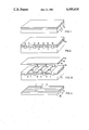
- FIGS. 1 and 2 are perspective views illustrating successive steps for manufacturing a pressure-sensitive transducer according the invention.
- FIG. 3 is a perspective view of one preferred embodiment of a pressure-sensitive transducer according to the invention.
- FIG. 4 is a perspective view of a special, alternative design of the row or column conductors in the pressure-sensitive transducer according to the invention.
- FIGS. 1-4 of the drawings The preferred embodiments of the present invention will now be described with reference to FIGS. 1-4 of the drawings. Identical elements in the various figures are designated with the same reference numerals.
- FIG. 1 shows a base plate or substrate 2.
- the thickness of this substrate will not substantially exceed 1000 micrometers and typically can be about 300 micrometers.
- the substrate can be formed of ceramic, aluminum oxide, lead-zirconate-titanate, a synthetic (plastic) material, or some other appropriate, non-conductive, support material.
- the substrate is provided with a metallization 4 suitable as an electrode.
- the metallization can consist of indium-tin (InSn), gold, or copper, for example, with a thickness not substantially exceeding 100 micrometers. Typically, the thickness is at most 10 micrometers.
- This metalization 4 is, in turn, provided with a coating layer 14 of a material having a high dielectric constant which is used as a dielectric medium.
- the layer 14 may consist of piezo-ceramic material or synthetic (plastic) material with embedded ceramic particles, preferably of lead-zirconate-titanate (PZT), with a relative dielectric constant of approximately 4000.
- PZT lead-zirconate-titanate
- the thickness of this layer does not much exceed 100 micrometers and is preferably between approximately 10 to 100 micrometers.
- a thickness of between approximately 5 to 100 micrometers is preferred.
- this double layer consisting of the metallization 4 and the dielectric medium 14 is divided into strip-shaped regions by cutting parallel grooves extending down to the substrate 2.
- the metallic portions of these regions each form a column conductor or electrode, identified in FIG. 2 by numbers 5 to 7, and are each covered by a similarly-structured dielectric layer 15 to 17.
- the grooves 12 are then filled with an electrically insulating material, preferably a self-hardening synthetic (plastic) material (e.g., Araldite), and the exposed surface is smoothed (e.g., ground down).
- plastic plastic
- the exposed surface is provided with a photo-sensitive layer 22, the thickness of which is at least 10 micrometers but which generally does not substantially exceed 100 micrometers.
- empty spaces 24, 25 and 26 are produced in this photo-sensitive layer 22 by photolithography in the customary manner.
- the remaining bar-shaped portions of the layer 22 form clearance spacers 28, 29, 30 and 31 for row conductors (electrodes) 35 and 36.
- These row conductors are preferably arranged at right angles to the column conductors 5, 6 and 7 above the clearance spacers 28-31 and can be attached to a cover 38, for example.
- the row conductors 35 and 36 consist generally of metal--gold or copper, for example--and can be appropriately applied by vapor deposition or sputtering to the flat underside of the cover 38, which can consist of a synthetic (plastic) layer (e.g., Kapton).
- the application of pressure on the cover 38 reduces the spacing at the crosspoint between the respective row conductor 35 or 36 and one of the column conductors 5-7 until contact is made with the associated dielectric layer strip 15-17 by the row conductor 35 or 36.
- This change in spacing and making contact effects a corresponding increase in the capacitance which, for example if lead-zirconate-titanate (PZT) with a relative dielectric constant of approximately 4000 is used as the dielectric medium, is at least one order of magnitude greater than the series capacitance formed by the air space and the dielectric layer when the device is in its quiescent state without the application of pressure.
- PZT lead-zirconate-titanate
- This change in capacitance is converted into a location-dependent electric signal by selecting the column and row electrodes.
- the row or column electrodes 35 and 36 can also consist of a so-called "interconnector" 40 which incorporates electrically insulating regions 41, 42 and 43, arranged parallel to each other in an elastomer. Each two adjacent ones of these regions confine between them a strip-shaped, electrically conductive region thus forming row electrodes 45 and 46.
- This interconnector is then applied to the clearance spacers 28-31 and can also be appropriately equipped with a cover.
Abstract
A pressure-sensitive transducer arrangement comprises a matrix of transducer elements which are formed at the points of intersection of row conductors (35, 36) and column conductors (5 to 7). A flat substrate (2) is provided with column conductors (5 to 7), each of which is covered with a similarly-structured piezoceramic material as a dielectric medium (15 to 17). This piezoceramic material is separated from the row electrode (35, 36) by empty spaces (24 to 26). Due to bilateral spacing of less than 100 micrometers for the row conductors and column conductors, a sensor matrix is produced with a dense packing of pressure-sensors functioning as capacitors which are formed at the cross-points of the row and column conductors. These sensors are particularly adapted for use in the gripping device of an industrial robot and make it possible to detect and determine the position of robot workpieces.
Description
The present invention concerns a pressure-sensitive transducer arrangement having a matrix of transducer elements formed at the points of intersection of rows and columns of conductors. This transducer arrangement is intended particularly for use with industrial robots.
The PCT International Patent Publication No. WO 81/02223 discloses a pressure-sensitive transducer which has a matrix of transducer elements formed at the crosspoints of rows and columns of conductors (electrodes). This transducer arrangement comprises two piezoelectric polymer film layers made of polyvinylidene fluoride (PVDF), one provided with rows of conductors and the other with columns of conductors, and an electrically insulated intermediate layer sandwiched between them. This sandwich configuration is covered on each of the two flat, outer sides by an electrically conductive layer. In addition, perforated sheets may be placed over the two outer sides. The signal is generated by piezoelectric effect as a result of strain due pressure on and bending of the piezoelectric layers.
In addition, capacitance-based pushbuttons (key) switches are known in which the compression of a dielectric medium causes a sudden change in capacitance. See, e.g., Elektronikschau, Vol. 9 (1980), p. 27. This change in capacitance is converted into pulses by means of appropriate circuitry. Since such keys have no mechanical contacts, they have a long useful life. Finally, tactile sensors are known that contain conductive elastomers, conductive synthetic (plastic) materials, pressure-sensitive switching diodes, or piezo-resistive elements, as well as pneumatic switches. Such sensors, which have applications in industrial robots, are disclosed in the article "Sensors For Computer Controlled Mechanical Assembly" by S. Wang et al., The Industrial Robot (March, 1978), pp. 9-18. In the case of these sensors, however, it is difficult to reduce the individual sensor elements to the required dimensions in a cost-effective manner in order to realize a matrix with a smaller grid line spacing and, thus, a higher resolution as to location.
An object of the present invention is to provide a tactile surface-sensor matrix which is useful, particularly, for industrial robots. Such a surface sensor can be inserted in the gripping device of a robot making it possible to detect and determine the position of the robot's workpieces.
A further object of the invention is to provide a tactile sensor--that is, a pressure-sensitive transducer--having a sensor grid or matrix that may be manufactured with an extremely small grid line spacing.
The invention is based on the knowledge that the high dielectric constant of certain piezoceramics--and in particular, of lead-zirconate-titanate (PZT)--makes it possible to produce a capacitive sensor matrix with very small grid line spacing.
According to the invention, a pressure-sensitive transducer is formed by providing a substrate; a set of strip-shaped column conductors disposed on the substrate surface and electrically insulated from each other; a set of strip-shaped dielectric elements formed of a piezoceramic material, with each dielectric element located over a corresponding one of the column conductors; and a set of strip-shaped row conductors located above the dielectric elements and separated from these dielectric elements by small empty spaces.
With a grid size formed by row and column conductors of a few hundred micrometers and the air space above the dielectric medium, a sensitive surface sensor is attained which can be manufactured in a simple manner.
In a special design of the pressure-sensitive transducer according to the invention, the row or column conductors not covered by the dielectric medium can can be embedded in a so-called "interconnector".
To produce the pressure-sensitive transducer just described, a thin base plate (substrate) is metallized and covered with the dielectric medium. Either the row or column conductors are produced from this double layer by etching parallel grooves in the metal and dielectric layers down to the base plate. Next, these grooves are filled with electrically insulating material such as a self-hardening plastic. The exposed surface is then smoothed--by grinding it down, for example--and provided with clearance spacers. Preferably, these clearance spacers are produced photolithographically from a photo-sensitive layer. The row or column conductors are then arranged on these clearance spacers and can be attached, for example, to a plastic layer serving as a cover.
The foregoing and other objects, features and advantages of the invention will be apparent from the following more particular description of the preferred embodiments of the invention, as illustrated in the accompanying drawing.
FIGS. 1 and 2 are perspective views illustrating successive steps for manufacturing a pressure-sensitive transducer according the invention.
FIG. 3 is a perspective view of one preferred embodiment of a pressure-sensitive transducer according to the invention.
FIG. 4 is a perspective view of a special, alternative design of the row or column conductors in the pressure-sensitive transducer according to the invention.
The preferred embodiments of the present invention will now be described with reference to FIGS. 1-4 of the drawings. Identical elements in the various figures are designated with the same reference numerals.
FIG. 1 shows a base plate or substrate 2. The thickness of this substrate will not substantially exceed 1000 micrometers and typically can be about 300 micrometers. The substrate can be formed of ceramic, aluminum oxide, lead-zirconate-titanate, a synthetic (plastic) material, or some other appropriate, non-conductive, support material. The substrate is provided with a metallization 4 suitable as an electrode. The metallization can consist of indium-tin (InSn), gold, or copper, for example, with a thickness not substantially exceeding 100 micrometers. Typically, the thickness is at most 10 micrometers. This metalization 4 is, in turn, provided with a coating layer 14 of a material having a high dielectric constant which is used as a dielectric medium.
In particular, the layer 14 may consist of piezo-ceramic material or synthetic (plastic) material with embedded ceramic particles, preferably of lead-zirconate-titanate (PZT), with a relative dielectric constant of approximately 4000. Generally, the thickness of this layer does not much exceed 100 micrometers and is preferably between approximately 10 to 100 micrometers. In the case of a synthetic (plastic) layer, a thickness of between approximately 5 to 100 micrometers is preferred.
As shown in FIG. 2, this double layer consisting of the metallization 4 and the dielectric medium 14 is divided into strip-shaped regions by cutting parallel grooves extending down to the substrate 2. The metallic portions of these regions each form a column conductor or electrode, identified in FIG. 2 by numbers 5 to 7, and are each covered by a similarly-structured dielectric layer 15 to 17. The grooves 12 are then filled with an electrically insulating material, preferably a self-hardening synthetic (plastic) material (e.g., Araldite), and the exposed surface is smoothed (e.g., ground down).
Finally, the exposed surface is provided with a photo-sensitive layer 22, the thickness of which is at least 10 micrometers but which generally does not substantially exceed 100 micrometers.
As shown in FIG. 3, empty spaces 24, 25 and 26 are produced in this photo-sensitive layer 22 by photolithography in the customary manner. The remaining bar-shaped portions of the layer 22 form clearance spacers 28, 29, 30 and 31 for row conductors (electrodes) 35 and 36. These row conductors are preferably arranged at right angles to the column conductors 5, 6 and 7 above the clearance spacers 28-31 and can be attached to a cover 38, for example. The row conductors 35 and 36 consist generally of metal--gold or copper, for example--and can be appropriately applied by vapor deposition or sputtering to the flat underside of the cover 38, which can consist of a synthetic (plastic) layer (e.g., Kapton).
The application of pressure on the cover 38 reduces the spacing at the crosspoint between the respective row conductor 35 or 36 and one of the column conductors 5-7 until contact is made with the associated dielectric layer strip 15-17 by the row conductor 35 or 36. This change in spacing and making contact effects a corresponding increase in the capacitance which, for example if lead-zirconate-titanate (PZT) with a relative dielectric constant of approximately 4000 is used as the dielectric medium, is at least one order of magnitude greater than the series capacitance formed by the air space and the dielectric layer when the device is in its quiescent state without the application of pressure. This change in capacitance is converted into a location-dependent electric signal by selecting the column and row electrodes.
According to the design shown in FIG. 4, the row or column electrodes 35 and 36 can also consist of a so-called "interconnector" 40 which incorporates electrically insulating regions 41, 42 and 43, arranged parallel to each other in an elastomer. Each two adjacent ones of these regions confine between them a strip-shaped, electrically conductive region thus forming row electrodes 45 and 46. This interconnector is then applied to the clearance spacers 28-31 and can also be appropriately equipped with a cover.
There has thus been shown and described a novel pressuresensitive transducer which fulfills all the objects and advantages sought therefor. Many changes, modifications, variations and other uses and applications of the subject invention will, however, become apparent to those skilled in the art after considering this specification and the accompanying drawing which discloses preferred embodiments thereof. All such changes, modifications, variations and other uses and applications which do not depart from the spirit and scope of the invention are deemed to be covered by the invention which is limited only by the claims which follow.
Claims (5)
1. A pressure-sensitive transducer arrangement comprising, in combination:
(a) a substrate having a substrate surface;
(b) a plurality of strip-shaped column conductors disposed on said substrate surface and electrically insulated from each other (;), succesive ones of said column conductors being spaced apart a maximum distance of a few hundred micrometers,
(c) a plurality strip-shaped dielectric elements formed of a piezoceramic material, each dielectric element being disposed over a corresponding one of said column conductors; and
(d) a plurality of strip-shaped row conductors disposed above said dielectric elements and separated therefrom at each crosspoint by an empty space, succesive ones of said row conductors being spaced apart a maximum distance of a few hundred micrometers;
whereby a matrix of transducer elements are formed at the crosspoints of said column and row conductors with a maximum grid size of a few hundred micrometers.
2. The transducer arrangement defined in claim 1, wherein said row conductors extend in a substantially perpendicular direction to said column conductors and said dielectric elements.
3. The transducer arrangement defined in claim 1, wherein said dielectric elements are made of lead-zirconate-titanate (PZT).
4. The transducer arrangement defined in any one of claims 1-3, wherein one of said sets of row or column electrodes are embedded in an interconnector.
5. The transducer arrangement defined in claim 1, wherein said dielectric elements are made of a plastic layer containing embedded piezoceramic particles.
Applications Claiming Priority (2)
| Application Number | Priority Date | Filing Date | Title |
|---|---|---|---|
| DE3236098 | 1982-09-29 | ||
| DE19823236098 DE3236098A1 (en) | 1982-09-29 | 1982-09-29 | PRESSURE CONVERTER ARRANGEMENT, ESPECIALLY FOR INDUSTRIAL ROBOTS |
Related Child Applications (1)
| Application Number | Title | Priority Date | Filing Date |
|---|---|---|---|
| US06/680,420 Division US4574438A (en) | 1982-09-29 | 1984-12-11 | Method of making pressure-sensitive transducer |
Publications (1)
| Publication Number | Publication Date |
|---|---|
| US4495434A true US4495434A (en) | 1985-01-22 |
Family
ID=6174484
Family Applications (2)
| Application Number | Title | Priority Date | Filing Date |
|---|---|---|---|
| US06/536,408 Expired - Fee Related US4495434A (en) | 1982-09-29 | 1983-09-27 | Pressure-sensitive transducer using piezo ceramic material |
| US06/680,420 Expired - Fee Related US4574438A (en) | 1982-09-29 | 1984-12-11 | Method of making pressure-sensitive transducer |
Family Applications After (1)
| Application Number | Title | Priority Date | Filing Date |
|---|---|---|---|
| US06/680,420 Expired - Fee Related US4574438A (en) | 1982-09-29 | 1984-12-11 | Method of making pressure-sensitive transducer |
Country Status (4)
| Country | Link |
|---|---|
| US (2) | US4495434A (en) |
| EP (1) | EP0104575B1 (en) |
| JP (1) | JPS5983024A (en) |
| DE (2) | DE3236098A1 (en) |
Cited By (30)
| Publication number | Priority date | Publication date | Assignee | Title |
|---|---|---|---|---|
| US4539554A (en) * | 1982-10-18 | 1985-09-03 | At&T Bell Laboratories | Analog integrated circuit pressure sensor |
| US4634917A (en) * | 1984-12-26 | 1987-01-06 | Battelle Memorial Institute | Active multi-layer piezoelectric tactile sensor apparatus and method |
| US4857916A (en) * | 1987-02-26 | 1989-08-15 | Bellin Robert W | System and method for identifying an individual utilizing grasping pressures |
| US5105650A (en) * | 1990-03-08 | 1992-04-21 | Gas Research Institute | Monitoring compaction of backfill |
| US5426972A (en) * | 1993-04-20 | 1995-06-27 | Gas Research Institute | Monitoring soil compaction |
| US5481246A (en) * | 1992-03-12 | 1996-01-02 | Verres Industries Sa | Alarm device having a pick-up formed as a condenser with piezoelectric dielectric |
| US5536990A (en) * | 1991-03-27 | 1996-07-16 | Thiokol Corporation | Piezoelectric igniter |
| US5808562A (en) * | 1991-09-25 | 1998-09-15 | U.S. Philips Corporation | Vehicle detector for installation on the surface of a multi-lane road |
| US6178246B1 (en) * | 1998-05-20 | 2001-01-23 | Daimlerchrysler Ag | Apparatus for the active suppression of noise radiated by a surface |
| US20020149571A1 (en) * | 2001-04-13 | 2002-10-17 | Roberts Jerry B. | Method and apparatus for force-based touch input |
| US20020175836A1 (en) * | 2001-04-13 | 2002-11-28 | Roberts Jerry B. | Tangential force control in a touch location device |
| US20030206162A1 (en) * | 2002-05-06 | 2003-11-06 | Roberts Jerry B. | Method for improving positioned accuracy for a determined touch input |
| US20030210235A1 (en) * | 2002-05-08 | 2003-11-13 | Roberts Jerry B. | Baselining techniques in force-based touch panel systems |
| US20030214485A1 (en) * | 2002-05-17 | 2003-11-20 | Roberts Jerry B. | Calibration of force based touch panel systems |
| US20030214486A1 (en) * | 2002-05-17 | 2003-11-20 | Roberts Jerry B. | Correction of memory effect errors in force-based touch panel systems |
| US20110048139A1 (en) * | 2009-08-31 | 2011-03-03 | Industrial Technology Research Institute | Micro-deformable piezoresistive material and manufacturing method thereof and pressure sensor using the same |
| US20140083196A1 (en) * | 2012-09-26 | 2014-03-27 | Haidou WANG | Smart coating and method for manufacturing the same |
| US20140311833A1 (en) * | 2013-04-17 | 2014-10-23 | Itt Italia S.R.L. | Method for manufacturing a braking element with integrated sensor, in particular a brake pad, brake pad with integrated sensor, vehicle braking system and associated method |
| US9381653B2 (en) | 2014-03-10 | 2016-07-05 | Samsung Electronics Co., Ltd. | Robot and substrate handling apparatus including the same |
| US20160197609A1 (en) * | 2013-08-09 | 2016-07-07 | Aito B.V. | Mounting arrangement for piezoelectric sensor device |
| US20170075467A1 (en) * | 2015-09-11 | 2017-03-16 | Korea Institute Of Science And Technology | Capacitive force sensor and method for preparing the same |
| US20170082167A1 (en) * | 2015-05-28 | 2017-03-23 | Itt Italia S.R.L. | Signal transducer devices, systems, and methods |
| WO2018081061A1 (en) * | 2016-10-25 | 2018-05-03 | Wal-Mart Stores, Inc. | Systems and methods of tracking products during transport |
| US10113598B2 (en) * | 2014-09-08 | 2018-10-30 | Itt Italia S.R.L. | Method for manufacturing a sensorized braking element, in particular a brake pad and a sensorized brake pad obtained thereby |
| US10227064B2 (en) | 2016-03-03 | 2019-03-12 | Itt Italia S.R.L. | Antilock braking systems, devices, and methods using sensorized brake pads |
| US10295006B2 (en) | 2015-09-17 | 2019-05-21 | Itt Italia S.R.L. | Hot runner detection and response systems, devices, and methods |
| US10495168B2 (en) | 2015-09-17 | 2019-12-03 | Itt Italia S.R.L. | Sensor-equipped vehicle braking systems, devices, and methods |
| US11441629B2 (en) | 2016-07-25 | 2022-09-13 | Itt Italia S.R.L. | Residual braking torque indication devices, systems, and methods |
| US11519475B2 (en) | 2019-09-06 | 2022-12-06 | Itt Italia S.R.L. | Vehicle brake pad and a production process thereof |
| US11740145B2 (en) | 2021-05-25 | 2023-08-29 | Itt Italia S.R.L. | Methods and devices for estimating residual torque between the braked and braking elements of a vehicle |
Families Citing this family (22)
| Publication number | Priority date | Publication date | Assignee | Title |
|---|---|---|---|---|
| DE3429607A1 (en) * | 1984-08-09 | 1986-02-20 | Klaus 1000 Berlin Oppermann | MEASURING VALUE FOR ELECTRICAL MEASUREMENT OF FORCES, PRESSURES AND TENSIONS |
| US4627533A (en) * | 1984-10-29 | 1986-12-09 | Hughes Aircraft Company | Ceramic package for compensated crystal oscillator |
| US5062198A (en) * | 1990-05-08 | 1991-11-05 | Keytec, Inc. | Method of making a transparent touch screen switch assembly |
| US5357399A (en) * | 1992-09-25 | 1994-10-18 | Avx Corporation | Mass production method for the manufacture of surface mount solid state capacitor and resulting capacitor |
| FR2700220B1 (en) * | 1993-01-06 | 1995-02-17 | Saint Louis Inst | Method for polarizing at least one zone of a sheet of ferroelectric material, and method for producing a polarized element for piezoelectric or pyroelectric sensor. |
| US5552923A (en) * | 1993-10-20 | 1996-09-03 | Daewoo Electronics Co., Ltd. | Array of electrodisplacive actuated mirrors and method for the manufacture thereof |
| US6337609B1 (en) * | 1997-07-17 | 2002-01-08 | Tdk Corporation | Delay compensation device, delay line component and manufacturing method of the delay line component |
| DE19806365A1 (en) * | 1998-02-09 | 1999-08-12 | Matthias Wapler | Pressure detection and localization system with special surface area |
| DE19826485A1 (en) * | 1998-06-13 | 2000-01-20 | Volkswagen Ag | Method and device for detecting pressure or force effects on a surface layer of an object |
| KR100608927B1 (en) * | 2005-05-26 | 2006-08-08 | 한국과학기술원 | Electrode layer for capacitor, method of manufacturing the electrode layer, unit sensor using the electrode layer and tactile sensor using the unit sensor |
| US7639237B2 (en) * | 2006-03-03 | 2009-12-29 | Perkins Michael T | Roll-out touch screen support system (ROTS3) |
| EP2010868B1 (en) * | 2006-03-28 | 2017-01-18 | University of Southern California | Biomimetic tactile sensor |
| US8181540B2 (en) * | 2006-03-28 | 2012-05-22 | University Of Southern California | Measurement of sliding friction-induced vibrations for biomimetic tactile sensing |
| US8272278B2 (en) * | 2007-03-28 | 2012-09-25 | University Of Southern California | Enhancements to improve the function of a biomimetic tactile sensor |
| US8169772B2 (en) | 2007-05-01 | 2012-05-01 | Avx Corporation | Precision laser adjustable thin film capacitors |
| JP2010528267A (en) | 2007-05-18 | 2010-08-19 | ユニバーシティ オブ サザン カリフォルニア | Biomimetic tactile sensor for grip control |
| US8006565B2 (en) * | 2009-04-30 | 2011-08-30 | Hewlett-Packard Development Company, L.P. | Pressure sensor grid |
| US9625333B2 (en) | 2013-03-15 | 2017-04-18 | President And Fellows Of Harvard College | Tactile sensor |
| EP3469323A4 (en) | 2016-06-08 | 2020-03-18 | The University of British Columbia | Surface sensor arrays using ionically conducting material |
| US10831319B2 (en) | 2017-02-09 | 2020-11-10 | The University Of British Columbia | Cluster sensor |
| US10670429B2 (en) | 2017-02-09 | 2020-06-02 | The University Of British Columbia | Capacitive bending sensors |
| JP7281630B2 (en) * | 2018-10-18 | 2023-05-26 | パナソニックIpマネジメント株式会社 | pressure sensitive devices and electronics |
Citations (10)
| Publication number | Priority date | Publication date | Assignee | Title |
|---|---|---|---|---|
| US3308253A (en) * | 1965-03-25 | 1967-03-07 | Ibm | Diaphragm switch having a diaphragm supported on an incompressible layer and an elastomer overlaying the diaphragm |
| US3350608A (en) * | 1963-09-21 | 1967-10-31 | Maltner Heinrich Gmbh | Piezo-electric igniter |
| US3653038A (en) * | 1970-02-20 | 1972-03-28 | United Bank Of Denver National | Capacitive electric signal device and keyboard using said device |
| US3750149A (en) * | 1972-01-18 | 1973-07-31 | Bell Telephone Labor Inc | Multi-unit electret touch selector |
| US3935485A (en) * | 1973-09-17 | 1976-01-27 | Kureha Kagaku Kogyo Kabushiki Kaisha | Piezoelectric key board switch |
| US3951250A (en) * | 1973-04-06 | 1976-04-20 | Alphameric Keyboards Limited | Capacitive key for electronic circuit |
| US4234813A (en) * | 1978-04-10 | 1980-11-18 | Toray Industries, Inc. | Piezoelectric or pyroelectric polymer input element for use as a transducer in keyboards |
| WO1981002223A1 (en) * | 1980-01-31 | 1981-08-06 | Minnesota Mining & Mfg | Pressure sensitive piezoelectric polymer signal generator |
| GB2070342A (en) * | 1979-12-27 | 1981-09-03 | Kureha Chemical Ind Co Ltd | Piezoelectric key-board units |
| US4412209A (en) * | 1981-11-20 | 1983-10-25 | W. H. Brady Co. | RC Array |
Family Cites Families (5)
| Publication number | Priority date | Publication date | Assignee | Title |
|---|---|---|---|---|
| US3118133A (en) * | 1960-04-05 | 1964-01-14 | Bell Telephone Labor Inc | Information storage matrix utilizing a dielectric of pressure changeable permittivity |
| JPS5410214B2 (en) * | 1973-10-15 | 1979-05-02 | ||
| DE2529475C3 (en) * | 1975-07-02 | 1981-10-08 | Ewald Max Christian Dipl.-Phys. 6000 Frankfurt Hennig | Electrical circuit arrangement for time-dependent measurement of physical quantities |
| AT355836B (en) * | 1977-02-10 | 1980-03-25 | Semperit Ag | CAPACITOR FOR MEASURING FORCES |
| GB1562766A (en) * | 1977-03-25 | 1980-03-19 | Electric Power Res Inst | Biaxial capacitance strain transducer |
-
1982
- 1982-09-29 DE DE19823236098 patent/DE3236098A1/en not_active Withdrawn
-
1983
- 1983-09-19 DE DE8383109266T patent/DE3377525D1/en not_active Expired
- 1983-09-19 EP EP83109266A patent/EP0104575B1/en not_active Expired
- 1983-09-27 US US06/536,408 patent/US4495434A/en not_active Expired - Fee Related
- 1983-09-28 JP JP58180071A patent/JPS5983024A/en active Pending
-
1984
- 1984-12-11 US US06/680,420 patent/US4574438A/en not_active Expired - Fee Related
Patent Citations (11)
| Publication number | Priority date | Publication date | Assignee | Title |
|---|---|---|---|---|
| US3350608A (en) * | 1963-09-21 | 1967-10-31 | Maltner Heinrich Gmbh | Piezo-electric igniter |
| US3308253A (en) * | 1965-03-25 | 1967-03-07 | Ibm | Diaphragm switch having a diaphragm supported on an incompressible layer and an elastomer overlaying the diaphragm |
| US3653038A (en) * | 1970-02-20 | 1972-03-28 | United Bank Of Denver National | Capacitive electric signal device and keyboard using said device |
| US3750149A (en) * | 1972-01-18 | 1973-07-31 | Bell Telephone Labor Inc | Multi-unit electret touch selector |
| US3951250A (en) * | 1973-04-06 | 1976-04-20 | Alphameric Keyboards Limited | Capacitive key for electronic circuit |
| US3935485A (en) * | 1973-09-17 | 1976-01-27 | Kureha Kagaku Kogyo Kabushiki Kaisha | Piezoelectric key board switch |
| US4234813A (en) * | 1978-04-10 | 1980-11-18 | Toray Industries, Inc. | Piezoelectric or pyroelectric polymer input element for use as a transducer in keyboards |
| GB2070342A (en) * | 1979-12-27 | 1981-09-03 | Kureha Chemical Ind Co Ltd | Piezoelectric key-board units |
| WO1981002223A1 (en) * | 1980-01-31 | 1981-08-06 | Minnesota Mining & Mfg | Pressure sensitive piezoelectric polymer signal generator |
| US4328441A (en) * | 1980-01-31 | 1982-05-04 | Minnesota Mining And Manufacturing Company | Output circuit for piezoelectric polymer pressure sensor |
| US4412209A (en) * | 1981-11-20 | 1983-10-25 | W. H. Brady Co. | RC Array |
Non-Patent Citations (3)
| Title |
|---|
| Elektronikschau, vol. 9, 1980, p. 27. * |
| The Industrial Robot, Mar. 1978, pp. 9 18. * |
| The Industrial Robot, Mar. 1978, pp. 9-18. |
Cited By (67)
| Publication number | Priority date | Publication date | Assignee | Title |
|---|---|---|---|---|
| US4539554A (en) * | 1982-10-18 | 1985-09-03 | At&T Bell Laboratories | Analog integrated circuit pressure sensor |
| US4634917A (en) * | 1984-12-26 | 1987-01-06 | Battelle Memorial Institute | Active multi-layer piezoelectric tactile sensor apparatus and method |
| US4857916A (en) * | 1987-02-26 | 1989-08-15 | Bellin Robert W | System and method for identifying an individual utilizing grasping pressures |
| US5105650A (en) * | 1990-03-08 | 1992-04-21 | Gas Research Institute | Monitoring compaction of backfill |
| US5402667A (en) * | 1990-03-08 | 1995-04-04 | Gas Research Institute | Monitoring of soil |
| US5536990A (en) * | 1991-03-27 | 1996-07-16 | Thiokol Corporation | Piezoelectric igniter |
| US5808562A (en) * | 1991-09-25 | 1998-09-15 | U.S. Philips Corporation | Vehicle detector for installation on the surface of a multi-lane road |
| US5481246A (en) * | 1992-03-12 | 1996-01-02 | Verres Industries Sa | Alarm device having a pick-up formed as a condenser with piezoelectric dielectric |
| US5426972A (en) * | 1993-04-20 | 1995-06-27 | Gas Research Institute | Monitoring soil compaction |
| US6178246B1 (en) * | 1998-05-20 | 2001-01-23 | Daimlerchrysler Ag | Apparatus for the active suppression of noise radiated by a surface |
| US7196694B2 (en) | 2001-04-13 | 2007-03-27 | 3M Innovative Properties Company | Force sensors and touch panels using same |
| US7190350B2 (en) | 2001-04-13 | 2007-03-13 | 3M Innovative Properties Company | Touch screen with rotationally isolated force sensor |
| US20020149571A1 (en) * | 2001-04-13 | 2002-10-17 | Roberts Jerry B. | Method and apparatus for force-based touch input |
| US20020175836A1 (en) * | 2001-04-13 | 2002-11-28 | Roberts Jerry B. | Tangential force control in a touch location device |
| US7183948B2 (en) | 2001-04-13 | 2007-02-27 | 3M Innovative Properties Company | Tangential force control in a touch location device |
| US20030206162A1 (en) * | 2002-05-06 | 2003-11-06 | Roberts Jerry B. | Method for improving positioned accuracy for a determined touch input |
| US7746325B2 (en) | 2002-05-06 | 2010-06-29 | 3M Innovative Properties Company | Method for improving positioned accuracy for a determined touch input |
| US20030210235A1 (en) * | 2002-05-08 | 2003-11-13 | Roberts Jerry B. | Baselining techniques in force-based touch panel systems |
| US7532202B2 (en) | 2002-05-08 | 2009-05-12 | 3M Innovative Properties Company | Baselining techniques in force-based touch panel systems |
| US20030214486A1 (en) * | 2002-05-17 | 2003-11-20 | Roberts Jerry B. | Correction of memory effect errors in force-based touch panel systems |
| US20070052690A1 (en) * | 2002-05-17 | 2007-03-08 | 3M Innovative Properties Company | Calibration of force based touch panel systems |
| US7176897B2 (en) | 2002-05-17 | 2007-02-13 | 3M Innovative Properties Company | Correction of memory effect errors in force-based touch panel systems |
| US7158122B2 (en) | 2002-05-17 | 2007-01-02 | 3M Innovative Properties Company | Calibration of force based touch panel systems |
| US20030214485A1 (en) * | 2002-05-17 | 2003-11-20 | Roberts Jerry B. | Calibration of force based touch panel systems |
| US20110048139A1 (en) * | 2009-08-31 | 2011-03-03 | Industrial Technology Research Institute | Micro-deformable piezoresistive material and manufacturing method thereof and pressure sensor using the same |
| US8371174B2 (en) * | 2009-08-31 | 2013-02-12 | Universal Cement Corporation | Micro-deformable piezoresistive material and manufacturing method thereof and pressure sensor using the same |
| US9046468B2 (en) * | 2012-09-26 | 2015-06-02 | Academy Of Armored Forces Engineering | Smart coating and method for manufacturing the same |
| US20140083196A1 (en) * | 2012-09-26 | 2014-03-27 | Haidou WANG | Smart coating and method for manufacturing the same |
| US20170030424A1 (en) * | 2013-04-17 | 2017-02-02 | Itt Italia S.R.L. | Vehicle braking systems and methods |
| US9964167B2 (en) * | 2013-04-17 | 2018-05-08 | Itt Italia S.R.L. | Vehicle braking systems and methods |
| US9415757B2 (en) * | 2013-04-17 | 2016-08-16 | Itt Italia S.R.L. | Method for manufacturing a braking element with integrated sensor, in particular a brake pad, brake pad with integrated sensor, vehicle braking system and associated method |
| US20140311833A1 (en) * | 2013-04-17 | 2014-10-23 | Itt Italia S.R.L. | Method for manufacturing a braking element with integrated sensor, in particular a brake pad, brake pad with integrated sensor, vehicle braking system and associated method |
| US11767896B2 (en) | 2013-04-17 | 2023-09-26 | Itt Italia S.R.L. | Vehicle braking systems and methods |
| US10598239B2 (en) * | 2013-04-17 | 2020-03-24 | Itt Italia S.R.L. | Vehicle braking systems and methods |
| US20180306262A1 (en) * | 2013-04-17 | 2018-10-25 | Itt Italia S.R.L. | Vehicle braking systems and methods |
| US20160197609A1 (en) * | 2013-08-09 | 2016-07-07 | Aito B.V. | Mounting arrangement for piezoelectric sensor device |
| US10193551B2 (en) * | 2013-08-09 | 2019-01-29 | Aito Bv | Mounting arrangement for piezoelectric sensor device |
| US9381653B2 (en) | 2014-03-10 | 2016-07-05 | Samsung Electronics Co., Ltd. | Robot and substrate handling apparatus including the same |
| US11168752B2 (en) * | 2014-09-08 | 2021-11-09 | Itt Italia S.R.L. | Method for manufacturing a sensorized braking element, in particular a brake pad and a sensorized brake pad obtained thereby |
| US10113598B2 (en) * | 2014-09-08 | 2018-10-30 | Itt Italia S.R.L. | Method for manufacturing a sensorized braking element, in particular a brake pad and a sensorized brake pad obtained thereby |
| US20170082166A1 (en) * | 2015-05-28 | 2017-03-23 | Itt Italia S.R.L. | Smart braking devices, systems, and methods with resin features |
| US11933379B2 (en) | 2015-05-28 | 2024-03-19 | Itt Italia S.R.L. | Smart braking devices, systems, and methods with resin features |
| US10138968B2 (en) * | 2015-05-28 | 2018-11-27 | Itt Italia S.R.L. | Signal transducer devices, systems, and methods |
| US9939035B2 (en) | 2015-05-28 | 2018-04-10 | Itt Italia S.R.L. | Smart braking devices, systems, and methods |
| US10208822B2 (en) | 2015-05-28 | 2019-02-19 | Itt Italia S.R.L. | Smart braking devices, systems, and methods with signal conditioners |
| US20170082167A1 (en) * | 2015-05-28 | 2017-03-23 | Itt Italia S.R.L. | Signal transducer devices, systems, and methods |
| US10408292B2 (en) | 2015-05-28 | 2019-09-10 | Itt Italia S.R.L. | Smart braking devices, systems, and methods |
| US10955017B2 (en) * | 2015-05-28 | 2021-03-23 | Itt Italia S.R.L. | Smart braking devices, systems, and methods with resin features |
| US10677304B2 (en) | 2015-05-28 | 2020-06-09 | Itt Italia S.R.L. | Smart braking devices, systems, and methods with signal conditioners |
| US20170075467A1 (en) * | 2015-09-11 | 2017-03-16 | Korea Institute Of Science And Technology | Capacitive force sensor and method for preparing the same |
| US9965077B2 (en) * | 2015-09-11 | 2018-05-08 | Korea Institute Of Science And Technology | Capacitive force sensor and method for preparing the same |
| US10295006B2 (en) | 2015-09-17 | 2019-05-21 | Itt Italia S.R.L. | Hot runner detection and response systems, devices, and methods |
| US11661987B2 (en) | 2015-09-17 | 2023-05-30 | Itt Italia S.R.L. | Sensor-equipped vehicle braking systems, devices, and methods |
| US10495168B2 (en) | 2015-09-17 | 2019-12-03 | Itt Italia S.R.L. | Sensor-equipped vehicle braking systems, devices, and methods |
| US11828333B2 (en) | 2015-09-17 | 2023-11-28 | Itt Italia S.R.L. | Hot runner detection and response systems, devices, and methods |
| US11047440B2 (en) * | 2015-09-17 | 2021-06-29 | Itt Italia S.R.L. | Hot runner detection and response systems, devices, and methods |
| US11794707B2 (en) | 2016-03-03 | 2023-10-24 | Itt Italia S.R.L. | Antilock braking systems, devices, and methods using sensorized brake pads |
| US10227064B2 (en) | 2016-03-03 | 2019-03-12 | Itt Italia S.R.L. | Antilock braking systems, devices, and methods using sensorized brake pads |
| US11441629B2 (en) | 2016-07-25 | 2022-09-13 | Itt Italia S.R.L. | Residual braking torque indication devices, systems, and methods |
| US10504343B2 (en) | 2016-10-25 | 2019-12-10 | Walmart Apollo, Llc | Systems and methods of tracking products during transport |
| GB2573060B (en) * | 2016-10-25 | 2022-05-04 | Walmart Apollo Llc | Systems and methods of tracking products during transport |
| US10347095B2 (en) * | 2016-10-25 | 2019-07-09 | Walmart Apollo, Llc | Systems and methods of tracking products during transport |
| GB2573060A (en) * | 2016-10-25 | 2019-10-23 | Walmart Apollo Llc | Systems and methods of tracking products during transport |
| WO2018081061A1 (en) * | 2016-10-25 | 2018-05-03 | Wal-Mart Stores, Inc. | Systems and methods of tracking products during transport |
| US11519475B2 (en) | 2019-09-06 | 2022-12-06 | Itt Italia S.R.L. | Vehicle brake pad and a production process thereof |
| US11885386B2 (en) | 2019-09-06 | 2024-01-30 | Itt Italia S.R.L. | Vehicle brake pad and a production process thereof |
| US11740145B2 (en) | 2021-05-25 | 2023-08-29 | Itt Italia S.R.L. | Methods and devices for estimating residual torque between the braked and braking elements of a vehicle |
Also Published As
| Publication number | Publication date |
|---|---|
| DE3377525D1 (en) | 1988-09-01 |
| EP0104575A3 (en) | 1986-12-10 |
| DE3236098A1 (en) | 1984-03-29 |
| EP0104575A2 (en) | 1984-04-04 |
| EP0104575B1 (en) | 1988-07-27 |
| JPS5983024A (en) | 1984-05-14 |
| US4574438A (en) | 1986-03-11 |
Similar Documents
| Publication | Publication Date | Title |
|---|---|---|
| US4495434A (en) | Pressure-sensitive transducer using piezo ceramic material | |
| US4975616A (en) | Piezoelectric transducer array | |
| US5315204A (en) | Piezoelectric snap action switch | |
| EP0044342B1 (en) | Pressure sensitive piezoelectric polymer signal generator | |
| EP1570415B1 (en) | Tactile sensor element and sensor array | |
| US4731694A (en) | Touch selection pad and method of manufacture | |
| EP0465231B1 (en) | Surface area contact pressure transducer | |
| US4234813A (en) | Piezoelectric or pyroelectric polymer input element for use as a transducer in keyboards | |
| US3940637A (en) | Polymeric piezoelectric key actuated device | |
| US5818683A (en) | Variable capacitor | |
| US5431064A (en) | Transducer array | |
| US20020152048A1 (en) | Capacitive two dimensional sensor | |
| US4633123A (en) | Piezoelectric polymer keyboard apparatus | |
| CN106547343B (en) | Sensor-integrated haptic device and method of manufacturing the same | |
| WO1990006568A1 (en) | Silicon tactile imaging array and method of making same | |
| WO1994019834A1 (en) | Monolithic prestressed ceramic devices and method for making same | |
| JPH0534615B2 (en) | ||
| US6924584B2 (en) | Piezoelectric transducers utilizing sub-diaphragms | |
| JPH0719975A (en) | Pressure sensor chip, tactile sensor and manufacture of tactile sensor | |
| JP2583615B2 (en) | Touch sensor | |
| JPS63128236A (en) | Pressing force sensor | |
| US7278327B2 (en) | Film based position and pressure sensor | |
| JPS62297735A (en) | Piezoelectric pressure distribution sensor | |
| US20230408348A1 (en) | Electrostatic capacity sensor | |
| JPH02291901A (en) | Tactile array sensor |
Legal Events
| Date | Code | Title | Description |
|---|---|---|---|
| AS | Assignment |
Owner name: SIEMENS AKTIENGESELLSCHAFT, BERLIN AND MUNICH, GER Free format text: ASSIGNMENT OF ASSIGNORS INTEREST.;ASSIGNORS:DIEPERS, HEINRICH;SCHEWE, HERBERT;REEL/FRAME:004218/0847 Effective date: 19831024 |
|
| FEPP | Fee payment procedure |
Free format text: PAYOR NUMBER ASSIGNED (ORIGINAL EVENT CODE: ASPN); ENTITY STATUS OF PATENT OWNER: LARGE ENTITY |
|
| FPAY | Fee payment |
Year of fee payment: 4 |
|
| REMI | Maintenance fee reminder mailed | ||
| LAPS | Lapse for failure to pay maintenance fees | ||
| FP | Lapsed due to failure to pay maintenance fee |
Effective date: 19930124 |
|
| STCH | Information on status: patent discontinuation |
Free format text: PATENT EXPIRED DUE TO NONPAYMENT OF MAINTENANCE FEES UNDER 37 CFR 1.362 |