US4532598A - Electron beam exposure system - Google Patents
Electron beam exposure system Download PDFInfo
- Publication number
- US4532598A US4532598A US06/386,301 US38630182A US4532598A US 4532598 A US4532598 A US 4532598A US 38630182 A US38630182 A US 38630182A US 4532598 A US4532598 A US 4532598A
- Authority
- US
- United States
- Prior art keywords
- pattern
- data
- sub
- stage
- input
- Prior art date
- Legal status (The legal status is an assumption and is not a legal conclusion. Google has not performed a legal analysis and makes no representation as to the accuracy of the status listed.)
- Expired - Lifetime
Links
Images


Classifications
-
- H—ELECTRICITY
- H01—ELECTRIC ELEMENTS
- H01J—ELECTRIC DISCHARGE TUBES OR DISCHARGE LAMPS
- H01J37/00—Discharge tubes with provision for introducing objects or material to be exposed to the discharge, e.g. for the purpose of examination or processing thereof
- H01J37/30—Electron-beam or ion-beam tubes for localised treatment of objects
- H01J37/302—Controlling tubes by external information, e.g. programme control
- H01J37/3023—Programme control
- H01J37/3026—Patterning strategy
-
- H—ELECTRICITY
- H01—ELECTRIC ELEMENTS
- H01L—SEMICONDUCTOR DEVICES NOT COVERED BY CLASS H10
- H01L21/00—Processes or apparatus adapted for the manufacture or treatment of semiconductor or solid state devices or of parts thereof
- H01L21/02—Manufacture or treatment of semiconductor devices or of parts thereof
- H01L21/04—Manufacture or treatment of semiconductor devices or of parts thereof the devices having at least one potential-jump barrier or surface barrier, e.g. PN junction, depletion layer or carrier concentration layer
- H01L21/18—Manufacture or treatment of semiconductor devices or of parts thereof the devices having at least one potential-jump barrier or surface barrier, e.g. PN junction, depletion layer or carrier concentration layer the devices having semiconductor bodies comprising elements of Group IV of the Periodic System or AIIIBV compounds with or without impurities, e.g. doping materials
- H01L21/30—Treatment of semiconductor bodies using processes or apparatus not provided for in groups H01L21/20 - H01L21/26
Landscapes
- Engineering & Computer Science (AREA)
- Chemical & Material Sciences (AREA)
- Analytical Chemistry (AREA)
- Physics & Mathematics (AREA)
- Condensed Matter Physics & Semiconductors (AREA)
- General Physics & Mathematics (AREA)
- Manufacturing & Machinery (AREA)
- Computer Hardware Design (AREA)
- Microelectronics & Electronic Packaging (AREA)
- Power Engineering (AREA)
- Electron Beam Exposure (AREA)
- Lasers (AREA)
Abstract
Description
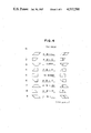
N→N'
H-L.sub.2 →H'
W-L.sub.2 →W'
X+L.sub.2 →X'
Y+L.sub.2 →Y'
N→N"
L.sub.2 →H"
W→W"
X→X"
Y→Y"
N→N'
H-L.sub.3 →H'
W-L.sub.3 →W'
X+L.sub.3 →X'
Y+L.sub.3 →Y'
L.sub.3 →H"
W-L.sub.3 /2→W"
X+L.sub.3 /2→X"
Y→Y"
Claims (13)
Applications Claiming Priority (2)
| Application Number | Priority Date | Filing Date | Title |
|---|---|---|---|
| JP56088183A JPS57204125A (en) | 1981-06-10 | 1981-06-10 | Electron-ray drawing device |
| JP56-88183 | 1981-06-10 |
Publications (1)
| Publication Number | Publication Date |
|---|---|
| US4532598A true US4532598A (en) | 1985-07-30 |
Family
ID=13935786
Family Applications (1)
| Application Number | Title | Priority Date | Filing Date |
|---|---|---|---|
| US06/386,301 Expired - Lifetime US4532598A (en) | 1981-06-10 | 1982-06-08 | Electron beam exposure system |
Country Status (5)
| Country | Link |
|---|---|
| US (1) | US4532598A (en) |
| EP (1) | EP0066882B1 (en) |
| JP (1) | JPS57204125A (en) |
| AT (1) | ATE60958T1 (en) |
| DE (1) | DE3280306D1 (en) |
Cited By (25)
| Publication number | Priority date | Publication date | Assignee | Title |
|---|---|---|---|---|
| US4837447A (en) * | 1986-05-06 | 1989-06-06 | Research Triangle Institute, Inc. | Rasterization system for converting polygonal pattern data into a bit-map |
| US4878177A (en) * | 1987-02-16 | 1989-10-31 | Kabushiki Kaisha Toshiba | Method for drawing a desired circuit pattern using charged particle beam |
| US4989156A (en) * | 1985-08-23 | 1991-01-29 | Kabushiki Kaisha Toshiba | Method of drawing a pattern on wafer with charged beam |
| US5030836A (en) * | 1988-08-05 | 1991-07-09 | Toshiba Machine Co., Ltd. | Method and apparatus for drawing patterns using an energy beam |
| US5159201A (en) * | 1991-07-26 | 1992-10-27 | International Business Machines Corporation | Shape decompositon system and method |
| US5210696A (en) * | 1989-02-10 | 1993-05-11 | Fujitsu Limited | Electron beam exposure data processing method, electron beam exposure method and apparatus |
| US5251140A (en) * | 1991-07-26 | 1993-10-05 | International Business Machines Corporation | E-beam control data compaction system and method |
| US5428552A (en) * | 1991-10-08 | 1995-06-27 | International Business Machines Corporation | Data compaction techniques for generation of a complex image |
| US5434795A (en) * | 1990-01-11 | 1995-07-18 | Fujitsu Limited | Method of forming pattern having optical angle in charged particle exposure system |
| US5500930A (en) * | 1988-11-04 | 1996-03-19 | Fujitsu Limited | System to decode instructions indicating the addresses of control codes and providing patterns to direct an electron beam exposure apparatus |
| US5563419A (en) * | 1994-05-25 | 1996-10-08 | Nec Corporation | Electron beam exposure system capable of correcting proximity effect |
| US5812412A (en) * | 1995-04-28 | 1998-09-22 | Mitsubishi Denki Kabushiki Kaisha | Charged beam pattern data generating method and a charged beam pattern data generating apparatus |
| US6060716A (en) * | 1997-03-28 | 2000-05-09 | Jeol Ltd. | Electron beam lithography method |
| US6275604B1 (en) * | 1998-03-16 | 2001-08-14 | Fujitsu Limited | Method and apparatus for generating semiconductor exposure data |
| US20020129324A1 (en) * | 1992-03-31 | 2002-09-12 | Iadonato Kevin R. | Integrated structure layout and layout of interconnections for an instruction execution unit of an integrated circuit chip |
| US20030107008A1 (en) * | 2001-10-26 | 2003-06-12 | Jeol Ltd. | Lithographic method using variable-area electron-beam lithography machine |
| US20050233227A1 (en) * | 2004-04-14 | 2005-10-20 | Baorui Yang | Methods for improving angled line feature accuracy and throughput using electron beam lithography and electron beam lithography system |
| US7516305B2 (en) | 1992-05-01 | 2009-04-07 | Seiko Epson Corporation | System and method for retiring approximately simultaneously a group of instructions in a superscalar microprocessor |
| US7558945B2 (en) | 1992-12-31 | 2009-07-07 | Seiko Epson Corporation | System and method for register renaming |
| US7685402B2 (en) | 1991-07-08 | 2010-03-23 | Sanjiv Garg | RISC microprocessor architecture implementing multiple typed register sets |
| US7739482B2 (en) | 1991-07-08 | 2010-06-15 | Seiko Epson Corporation | High-performance, superscalar-based computer system with out-of-order instruction execution |
| US7802074B2 (en) | 1992-03-31 | 2010-09-21 | Sanjiv Garg | Superscalar RISC instruction scheduling |
| US8074052B2 (en) | 1992-12-31 | 2011-12-06 | Seiko Epson Corporation | System and method for assigning tags to control instruction processing in a superscalar processor |
| US20160118221A1 (en) * | 2014-10-27 | 2016-04-28 | Canon Kabushiki Kaisha | Lithography system and method of manufacturing articles |
| US20160126062A1 (en) * | 2014-10-27 | 2016-05-05 | Canon Kabushiki Kaisha | Drawing apparatus, lithography system, pattern data creation method, drawing method, and method of manufacturing articles |
Families Citing this family (6)
| Publication number | Priority date | Publication date | Assignee | Title |
|---|---|---|---|---|
| JPS60196939A (en) * | 1984-03-19 | 1985-10-05 | Fujitsu Ltd | Charged particle beam exposure |
| JP2680295B2 (en) * | 1984-03-22 | 1997-11-19 | 株式会社東芝 | Method and apparatus for drawing data of electron beam exposure apparatus |
| JP2710162B2 (en) * | 1988-12-13 | 1998-02-10 | 株式会社東芝 | Method and apparatus for creating charged beam drawing data |
| US5446649A (en) * | 1992-12-31 | 1995-08-29 | International Business Machines Corporation | Data-hiding and skew scan for unioning of shapes in electron beam lithography post-processing |
| GB2334597B (en) * | 1995-04-28 | 1999-11-17 | Mitsubishi Electric Corp | A charged beam pattern data generating method and a charged beam pattern data generating apparatus |
| JP5658997B2 (en) * | 2010-12-17 | 2015-01-28 | 株式会社ニューフレアテクノロジー | Charged particle beam drawing apparatus and drawing data generation method |
Citations (10)
| Publication number | Priority date | Publication date | Assignee | Title |
|---|---|---|---|---|
| US3894271A (en) * | 1973-08-31 | 1975-07-08 | Ibm | Method and apparatus for aligning electron beams |
| US4145597A (en) * | 1975-12-31 | 1979-03-20 | Fujitsu Limited | Electron beam lithographic system |
| US4147937A (en) * | 1977-11-01 | 1979-04-03 | Fujitsu Limited | Electron beam exposure system method and apparatus |
| US4151422A (en) * | 1977-06-30 | 1979-04-24 | Rikagaku Kenkyusho | Electron beam exposure method |
| US4167676A (en) * | 1978-02-21 | 1979-09-11 | Bell Telephone Laboratories, Incorporated | Variable-spot scanning in an electron beam exposure system |
| US4213053A (en) * | 1978-11-13 | 1980-07-15 | International Business Machines Corporation | Electron beam system with character projection capability |
| US4280186A (en) * | 1978-07-07 | 1981-07-21 | Tokyo Shibaura Denki Kabushiki Kaisha | Exposure apparatus using electron beams |
| US4291231A (en) * | 1977-12-30 | 1981-09-22 | Fujitsu Limited | Electron beam exposure system and an apparatus for carrying out the same |
| US4393312A (en) * | 1976-02-05 | 1983-07-12 | Bell Telephone Laboratories, Incorporated | Variable-spot scanning in an electron beam exposure system |
| US4424448A (en) * | 1979-12-26 | 1984-01-03 | Tokyo Shibaura Denki Kabushiki Kaisha | Electron beam apparatus |
Family Cites Families (2)
| Publication number | Priority date | Publication date | Assignee | Title |
|---|---|---|---|---|
| JPS5473577A (en) * | 1977-11-24 | 1979-06-12 | Fujitsu Ltd | Electron beam exposure method |
| JPS5712520A (en) * | 1980-06-26 | 1982-01-22 | Nippon Telegr & Teleph Corp <Ntt> | Dividing method of figure by exposing in electron beam radiation |
-
1981
- 1981-06-10 JP JP56088183A patent/JPS57204125A/en active Granted
-
1982
- 1982-06-08 EP EP82105022A patent/EP0066882B1/en not_active Expired - Lifetime
- 1982-06-08 AT AT82105022T patent/ATE60958T1/en not_active IP Right Cessation
- 1982-06-08 DE DE8282105022T patent/DE3280306D1/en not_active Expired - Lifetime
- 1982-06-08 US US06/386,301 patent/US4532598A/en not_active Expired - Lifetime
Patent Citations (10)
| Publication number | Priority date | Publication date | Assignee | Title |
|---|---|---|---|---|
| US3894271A (en) * | 1973-08-31 | 1975-07-08 | Ibm | Method and apparatus for aligning electron beams |
| US4145597A (en) * | 1975-12-31 | 1979-03-20 | Fujitsu Limited | Electron beam lithographic system |
| US4393312A (en) * | 1976-02-05 | 1983-07-12 | Bell Telephone Laboratories, Incorporated | Variable-spot scanning in an electron beam exposure system |
| US4151422A (en) * | 1977-06-30 | 1979-04-24 | Rikagaku Kenkyusho | Electron beam exposure method |
| US4147937A (en) * | 1977-11-01 | 1979-04-03 | Fujitsu Limited | Electron beam exposure system method and apparatus |
| US4291231A (en) * | 1977-12-30 | 1981-09-22 | Fujitsu Limited | Electron beam exposure system and an apparatus for carrying out the same |
| US4167676A (en) * | 1978-02-21 | 1979-09-11 | Bell Telephone Laboratories, Incorporated | Variable-spot scanning in an electron beam exposure system |
| US4280186A (en) * | 1978-07-07 | 1981-07-21 | Tokyo Shibaura Denki Kabushiki Kaisha | Exposure apparatus using electron beams |
| US4213053A (en) * | 1978-11-13 | 1980-07-15 | International Business Machines Corporation | Electron beam system with character projection capability |
| US4424448A (en) * | 1979-12-26 | 1984-01-03 | Tokyo Shibaura Denki Kabushiki Kaisha | Electron beam apparatus |
Non-Patent Citations (2)
| Title |
|---|
| Fujinami et al., Precision Electron Beam Exposure System EB 52, Review of the Electrical Communications Laboratories, vol. 27, 1 2, (1,2/79), pp. 97 104. * |
| Fujinami et al., Precision Electron Beam Exposure System EB52, Review of the Electrical Communications Laboratories, vol. 27, #1-2, (1,2/79), pp. 97-104. |
Cited By (43)
| Publication number | Priority date | Publication date | Assignee | Title |
|---|---|---|---|---|
| US4989156A (en) * | 1985-08-23 | 1991-01-29 | Kabushiki Kaisha Toshiba | Method of drawing a pattern on wafer with charged beam |
| US4837447A (en) * | 1986-05-06 | 1989-06-06 | Research Triangle Institute, Inc. | Rasterization system for converting polygonal pattern data into a bit-map |
| US4878177A (en) * | 1987-02-16 | 1989-10-31 | Kabushiki Kaisha Toshiba | Method for drawing a desired circuit pattern using charged particle beam |
| US5030836A (en) * | 1988-08-05 | 1991-07-09 | Toshiba Machine Co., Ltd. | Method and apparatus for drawing patterns using an energy beam |
| US5500930A (en) * | 1988-11-04 | 1996-03-19 | Fujitsu Limited | System to decode instructions indicating the addresses of control codes and providing patterns to direct an electron beam exposure apparatus |
| US5210696A (en) * | 1989-02-10 | 1993-05-11 | Fujitsu Limited | Electron beam exposure data processing method, electron beam exposure method and apparatus |
| US5434795A (en) * | 1990-01-11 | 1995-07-18 | Fujitsu Limited | Method of forming pattern having optical angle in charged particle exposure system |
| US7941636B2 (en) | 1991-07-08 | 2011-05-10 | Intellectual Venture Funding Llc | RISC microprocessor architecture implementing multiple typed register sets |
| US7685402B2 (en) | 1991-07-08 | 2010-03-23 | Sanjiv Garg | RISC microprocessor architecture implementing multiple typed register sets |
| US7739482B2 (en) | 1991-07-08 | 2010-06-15 | Seiko Epson Corporation | High-performance, superscalar-based computer system with out-of-order instruction execution |
| US5251140A (en) * | 1991-07-26 | 1993-10-05 | International Business Machines Corporation | E-beam control data compaction system and method |
| US5159201A (en) * | 1991-07-26 | 1992-10-27 | International Business Machines Corporation | Shape decompositon system and method |
| US5428552A (en) * | 1991-10-08 | 1995-06-27 | International Business Machines Corporation | Data compaction techniques for generation of a complex image |
| US20040243961A1 (en) * | 1992-03-31 | 2004-12-02 | Seiko Epson Corporation | Integrated structure layout and layout of interconnections for an instruction execution unit of an integrated circuit chip |
| US20070113214A1 (en) * | 1992-03-31 | 2007-05-17 | Seiko Epson Corporation | Integrated structure layout and layout of interconnections for an instruction execution unit of an integrated circuit chip |
| US7555738B2 (en) | 1992-03-31 | 2009-06-30 | Seiko Epson Corporation | Integrated structure layout and layout of interconnections for an instruction execution unit of an integrated circuit chip |
| US20020129324A1 (en) * | 1992-03-31 | 2002-09-12 | Iadonato Kevin R. | Integrated structure layout and layout of interconnections for an instruction execution unit of an integrated circuit chip |
| US6782521B2 (en) * | 1992-03-31 | 2004-08-24 | Seiko Epson Corporation | Integrated structure layout and layout of interconnections for an instruction execution unit of an integrated circuit chip |
| US7174525B2 (en) | 1992-03-31 | 2007-02-06 | Seiko Epson Corporation | Integrated structure layout and layout of interconnections for an instruction execution unit of an integrated circuit chip |
| US7802074B2 (en) | 1992-03-31 | 2010-09-21 | Sanjiv Garg | Superscalar RISC instruction scheduling |
| US7523296B2 (en) | 1992-05-01 | 2009-04-21 | Seiko Epson Corporation | System and method for handling exceptions and branch mispredictions in a superscalar microprocessor |
| US7934078B2 (en) | 1992-05-01 | 2011-04-26 | Seiko Epson Corporation | System and method for retiring approximately simultaneously a group of instructions in a superscalar microprocessor |
| US7958337B2 (en) | 1992-05-01 | 2011-06-07 | Seiko Epson Corporation | System and method for retiring approximately simultaneously a group of instructions in a superscalar microprocessor |
| US7516305B2 (en) | 1992-05-01 | 2009-04-07 | Seiko Epson Corporation | System and method for retiring approximately simultaneously a group of instructions in a superscalar microprocessor |
| US7979678B2 (en) | 1992-12-31 | 2011-07-12 | Seiko Epson Corporation | System and method for register renaming |
| US8074052B2 (en) | 1992-12-31 | 2011-12-06 | Seiko Epson Corporation | System and method for assigning tags to control instruction processing in a superscalar processor |
| US7558945B2 (en) | 1992-12-31 | 2009-07-07 | Seiko Epson Corporation | System and method for register renaming |
| US5563419A (en) * | 1994-05-25 | 1996-10-08 | Nec Corporation | Electron beam exposure system capable of correcting proximity effect |
| US5812412A (en) * | 1995-04-28 | 1998-09-22 | Mitsubishi Denki Kabushiki Kaisha | Charged beam pattern data generating method and a charged beam pattern data generating apparatus |
| US6060716A (en) * | 1997-03-28 | 2000-05-09 | Jeol Ltd. | Electron beam lithography method |
| US6275604B1 (en) * | 1998-03-16 | 2001-08-14 | Fujitsu Limited | Method and apparatus for generating semiconductor exposure data |
| US6753540B2 (en) * | 2001-10-26 | 2004-06-22 | Jeol Ltd. | Lithographic method using variable-area electron-beam lithography machine |
| US20030107008A1 (en) * | 2001-10-26 | 2003-06-12 | Jeol Ltd. | Lithographic method using variable-area electron-beam lithography machine |
| US7759660B2 (en) | 2004-04-14 | 2010-07-20 | Micron Technology, Inc. | Electron beam lithography system |
| US20050233227A1 (en) * | 2004-04-14 | 2005-10-20 | Baorui Yang | Methods for improving angled line feature accuracy and throughput using electron beam lithography and electron beam lithography system |
| US7229742B2 (en) | 2004-04-14 | 2007-06-12 | Micron Technology, Inc. | Methods for improving angled line feature accuracy and throughput using electron beam lithography and electron beam lithography system |
| US20070003874A1 (en) * | 2004-04-14 | 2007-01-04 | Baorui Yang | Methods for improving angled line feature accuracy and throughput using electron beam lithography and electron beam lithography system |
| US20070102651A1 (en) * | 2004-04-14 | 2007-05-10 | Baorui Yang | Methods for improving angled line feature accuracy and throughput using electron beam lithography and electron beam lithography system |
| US7226723B2 (en) | 2004-04-14 | 2007-06-05 | Micron Technology, Inc. | Methods for improving angled line feature accuracy and throughput using electron beam lithography and electron beam lithography system |
| US20160118221A1 (en) * | 2014-10-27 | 2016-04-28 | Canon Kabushiki Kaisha | Lithography system and method of manufacturing articles |
| US20160126062A1 (en) * | 2014-10-27 | 2016-05-05 | Canon Kabushiki Kaisha | Drawing apparatus, lithography system, pattern data creation method, drawing method, and method of manufacturing articles |
| US9558916B2 (en) * | 2014-10-27 | 2017-01-31 | Canon Kabushiki Kaisha | Lithography system and method of manufacturing articles |
| US9583311B2 (en) * | 2014-10-27 | 2017-02-28 | Canon Kabushiki Kaisha | Drawing apparatus, lithography system, pattern data creation method, drawing method, and method of manufacturing articles |
Also Published As
| Publication number | Publication date |
|---|---|
| DE3280306D1 (en) | 1991-03-28 |
| JPS57204125A (en) | 1982-12-14 |
| ATE60958T1 (en) | 1991-03-15 |
| EP0066882A2 (en) | 1982-12-15 |
| EP0066882A3 (en) | 1985-06-05 |
| EP0066882B1 (en) | 1991-02-20 |
| JPS6239818B2 (en) | 1987-08-25 |
Similar Documents
| Publication | Publication Date | Title |
|---|---|---|
| US4532598A (en) | Electron beam exposure system | |
| EP0298275B1 (en) | Pattern splicing system and method for scanning of electron beam system | |
| EP0002957B1 (en) | Electron beam exposure apparatus | |
| EP0104922A2 (en) | Electron beam exposure system | |
| US20050285054A1 (en) | Charged particle beam drawing apparatus | |
| JP4054445B2 (en) | Charged beam drawing method | |
| JPS59136874A (en) | Pattern identifier | |
| JP3159810B2 (en) | Electron beam drawing method and apparatus | |
| US6314554B1 (en) | Method of generating mask pattern data for graphics and apparatus for the same | |
| US4468566A (en) | Corpuscular beam control circuit arrangement | |
| US5206517A (en) | Electron beam lithographic method | |
| JP2661739B2 (en) | Electron beam exposure method | |
| US6535222B1 (en) | Graphic method | |
| JP3983188B2 (en) | Parallel processing method of inverse matrix for shared memory type scalar parallel computer | |
| JP3408010B2 (en) | Pattern developing method and apparatus for charged particle beam exposure apparatus | |
| JP2697943B2 (en) | Processing method of writing data in charged particle beam writing | |
| JPH04137614A (en) | Method of lithography using charged beam | |
| Mlekus et al. | Polygonal geometry reconstruction after cellular etching or deposition simulation | |
| JPS6390827A (en) | Method and equipment of charged particle beam lithography | |
| JP2857260B2 (en) | Judgment method of rectangular area | |
| JPS58155474A (en) | Drawing method of parallel curve | |
| JPH11329958A (en) | Charged particle beam aligner | |
| JPH01152726A (en) | Charged particle beam lithography | |
| JP3083573B2 (en) | How to create charged beam drawing data | |
| JPH11260691A (en) | Electron beam lithography system |
Legal Events
| Date | Code | Title | Description |
|---|---|---|---|
| AS | Assignment |
Owner name: NIPPON TELEGRAPH & TELEPHONE PUBLIC CORPORATION Free format text: ASSIGNMENT OF ASSIGNORS INTEREST.;ASSIGNORS:SHIBAYAMA, AKINORI;FUJINAMI, MINPAI;YODA, HARUO;REEL/FRAME:004011/0429 Effective date: 19820601 Owner name: HITACHI, LTD. Free format text: ASSIGNMENT OF ASSIGNORS INTEREST.;ASSIGNORS:SHIBAYAMA, AKINORI;FUJINAMI, MINPAI;YODA, HARUO;REEL/FRAME:004011/0429 Effective date: 19820601 |
|
| STCF | Information on status: patent grant |
Free format text: PATENTED CASE |
|
| AS | Assignment |
Owner name: NIPPON TELEGRAPH & TELEPHONE CORPORATION Free format text: CHANGE OF NAME;ASSIGNOR:NIPPON TELEGRAPH AND TELEPHONE PUBLIC CORPORATION;REEL/FRAME:004454/0001 Effective date: 19850718 |
|
| FPAY | Fee payment |
Year of fee payment: 4 |
|
| FEPP | Fee payment procedure |
Free format text: PAYOR NUMBER ASSIGNED (ORIGINAL EVENT CODE: ASPN); ENTITY STATUS OF PATENT OWNER: LARGE ENTITY |
|
| FPAY | Fee payment |
Year of fee payment: 8 |
|
| FPAY | Fee payment |
Year of fee payment: 12 |