US4538245A - Enabling circuit for redundant word lines in a semiconductor memory array - Google Patents
Enabling circuit for redundant word lines in a semiconductor memory array Download PDFInfo
- Publication number
- US4538245A US4538245A US06/367,331 US36733182A US4538245A US 4538245 A US4538245 A US 4538245A US 36733182 A US36733182 A US 36733182A US 4538245 A US4538245 A US 4538245A
- Authority
- US
- United States
- Prior art keywords
- programming
- circuit
- set forth
- word line
- circuit structure
- Prior art date
- Legal status (The legal status is an assumption and is not a legal conclusion. Google has not performed a legal analysis and makes no representation as to the accuracy of the status listed.)
- Expired - Lifetime
Links
Images


Classifications
-
- G—PHYSICS
- G11—INFORMATION STORAGE
- G11C—STATIC STORES
- G11C29/00—Checking stores for correct operation ; Subsequent repair; Testing stores during standby or offline operation
- G11C29/70—Masking faults in memories by using spares or by reconfiguring
- G11C29/78—Masking faults in memories by using spares or by reconfiguring using programmable devices
- G11C29/838—Masking faults in memories by using spares or by reconfiguring using programmable devices with substitution of defective spares
-
- G—PHYSICS
- G11—INFORMATION STORAGE
- G11C—STATIC STORES
- G11C29/00—Checking stores for correct operation ; Subsequent repair; Testing stores during standby or offline operation
- G11C29/70—Masking faults in memories by using spares or by reconfiguring
- G11C29/78—Masking faults in memories by using spares or by reconfiguring using programmable devices
- G11C29/835—Masking faults in memories by using spares or by reconfiguring using programmable devices with roll call arrangements for redundant substitutions
Definitions
- the present invention relates to peripheral circuits for use with semiconductor memories employing MOS storage devices arranged in primary and redundant array configuration and is more particularly directed to a circuit which enables the redundant word lines in the redundant array for the purpose of providing back-up storage capacity should any of the storage devices in the primary array fail.
- a typical MOS floating gate storage device includes a floating gate structure disposed over the surface of a semiconductor substrate between spaced-apart source and drain regions. A control gate is then vertically aligned with the floating gate. In order to program the storage device, a potential is applied to the control gate such that charge carriers are transported between the semiconductor substrate and the floating gate, whereupon the threshold voltage in the channel region established between the spaced-apart source and drain regions is modified.
- the presence or absence of charge carriers on the floating gate can be determined by simply measuring the presence or absence of current flow through the channel region in response to voltage potentials applied to the drain region.
- floating gate storage devices of the type described above When floating gate storage devices of the type described above are incorporated in a semiconductor memory array, individual floating gates are utilized for each storage device while a single conductive strip is generally etched to define the control gates for all of the storage devices in a single memory array row.
- This single conductive strip is commonly known as a word line.
- the memory array is prepared for programming or read operations by enabling the word line of a particular memory array row using a unique x-address applied to the address inputs of the memory array.
- defects in various storage devices positioned along one or more rows in the memory array may occur, giving rise to erroneous data read-outs when the word line connected to the defective storage devices are addressed.
- a semiconductor memory which employs floating gate storage devices arranged to form a primary array and a redundant array such that storage devices in the redundant array can be activated to replace defective storage devices in the primary array.
- the control gates of the storage devices in the redundant array are connected to redundant word lines enabled by a redundancy decoder.
- that particular x-address can be programmed into the redundancy decoder by blowing selected polysilicon fuses in a series of fusible link circuits tied to a selected redundant word line such that subsequent addressing of the faulty primary word line instead enables the selected redundant word line.
- a redundancy disable circuit prevents any accidental reprogramming of the redundancy decoder with respect to the selected redundant word line.
- the redundancy disable circuit also generates a redundancy disable signal indicative of the fact that the selected redundant word line is in use, which redundancy disable signal can be supplied to an appropriate output contact of the semiconductor memory.
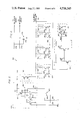
- FIG. 1 is a schematic representation of a semiconductor memory comprising floating gate storage devices arranged along primary and redundant word lines to form primary and redundant arrays;
- FIG. 2 is a circuit diagram of a dual-function address buffer capable of generating control signals for use in the redundancy decoder and redundancy disable circuit of the present invention
- FIG. 3 is a circuit diagram of the redundancy decoder which enables the redundant word lines of the redundant array illustrated in FIG. 1, the redundancy decoder including a circuit means for disabling the primary word lines in the primary array of the FIG. 1 memory whenever any one of the redundant word lines in the redundant array of the present invention is enabled;
- FIG. 4 is a circuit diagram of a redundancy disable circuit which prevents accidental reprogramming of the redundancy decoder illustrate,d in FIG. 3;
- FIG. 5 is an alternate embodiment of a redundancy decoder utilized with the redundant array of FIG. 1;
- FIG. 6 depicts a circuit configuration designed to permit substitution of one redundant word line for another in the redundant array of FIG. 1.
- FIG. 1 schematically illustrates a semiconductor memory having a plurality of MOS storage devices 4 arranged to form a primary array 6.
- Each of the storage devices 4 comprises an electrically-programmable read-only floating gate structure of the type disclosed in U.S. Pat. No. 4,075,045.
- a series of bit lines 8 arranged in columns and primary word lines 10 arranged in rows are respectively connected to the storage device drains 12 and control gates 14, whereby each storage device may be individually programmed and read in accordance with a unique storage device address.
- primary word lines 10 serve to define the x-addresses of the storage devices while bit lines 8 serve to define the storage device y-addresses.
- memory 2 includes two hundred and fifty-six primary word lines designated X 1 , X 2 . . . X 256 and two hundred and fifty-six bit lines designated Y 1 , Y 2 . . . Y 256 .
- the bit lines can be subdivided into eight groups of 32 bit lines each to enable the simultaneous storage of an 8-data bit word, i.e., a data byte, using only a single y-address.
- each of the eight bit lines activated by the single y-address may be arranged in interleaved fashion.
- Programming or reading of a particular storage device, or set of storage devices where bit lines 8 are divided into interleaved groups, is initiated by applying a digital address signal A 0 , A 1 . . . A n to a series of address bit inputs 16.
- the first five address bits A 0 -A 4 establish the particular y-address Y 1 , Y 2 . . . Y 32 of each data byte while an additional eight address bits A 5 -A 12 establish the data byte x-address X 1 , X 2 . . . X 256 .
- Address bit inputs 16 respectively feed the address bits A 0 -A 12 to a series of address buffers 18.
- Each of the address buffers in turn generates an address indicator AI i and an inverted address indicator AI i , for use in decoding the address signal. That is, the output of the address buffers 18 which receive address bits A 0 -A 4 comprise a series of address indicators AI 0 -AI 4 and inverted address indicators AI 0 -AI 4 , whereas the output of the address buffers 18 which receive address bits A 5 -A 12 comprise a series of address indicators AI 5 -AI 12 and inverted address indicators AI 5 -AI 12 .
- Address indicators AI 5 -AI 12 and inverted address indicators AI 5 -AI 12 are supplied to X-decoders schematically illustrated at 20 and are combined in a digital logic system to enable the specific primary word line 10 associated with the x-address established by address bits A 5 -A 12 .
- the address indicators AI 0 -AI 4 and inverted address indicators AI 0 -AI 4 are supplied to Y-decoders illustrated schematically at 22.
- the Y-decoders operate in conjunction with a column decoder 24, combining the various address and inverted address indicators in a digital logic system such that selected bit lines 8 associated with the y-address established by data bits A 0 -A 4 are enabled.
- Data is then programmed into or read out of primary array 6 by connecting each enabled bit line 8 to the appropriate one of a pair of input/output buffers 26 respectively tied to output pads 28 and then entering or reading out the appropriate data bit O 0 -O 7 .
- the time required to program individual storage devices 4 in primary array 6 can be significantly reduced by increasing the programming voltage present on the primary word lines 10 associated with the individual storage devices 4.
- a series of word line charge pumps 30 driven by a high voltage oscillator 31 are respectively connected to primary word lines 10 in order to raise the voltages thereof to a predetermined level during memory programming operations.
- Memory 2 is additionally provided with a redundant array 32 of storage devices 4 arranged along redundant word lines 34 for the purpose of providing back-up storage capacity should any of the primary word lines 10 in primary array 6 prove faulty, i.e., should any of the storage devices 4 associated with primary word lines 10 contain manufacturing defects.
- the redundant word lines 34 are connected to the control gates 14 of storage devices 4 to establish alternate x-addresses for the memory.
- address indicators AI 5 -AI 12 and inverted address indicators AI 5 -AI 12 generated by address buffers 18 as a function of the address bits A 5 -A 12 corresponding to the x-address of the faulty primary word line are used to program a redundancy decoder 36 such that any subsequent address signal A 0 -A 12 having the x-address of the faulty word line in primary array 6 will instead enable a selected redundant word line 34 in redundant array 32.
- a series of control signals supplied to redundancy select lines 37 via the output pads 28 associated with data bits O 0 -O 3 are gated through a set of redundancy enable transistors 38 to assist in programming redundancy decoder 36.
- a redundancy disable circuit 39 prevents any accidental reprogramming of redundancy decoder 36 relative to the selected redundant word line 34 enabled by the particular x-address.
- the redundancy disable circuit additionally generates a redundancy disable signal RD 1 -RD 4 indicative of the fact that the selected redundant word line is in use, which redundancy disable signal can be supplied back through redundancy enable transistors 38 to an appropriate output pad 28.
- the address buffers 18 employed in the memory 2 of the present invention may be constructed with a dual function capability, providing control signals for governing the operation of various peripheral circuits of the memory in addition to the aforementioned address and inverted address indicators AI 0 -AI 12 , AI 0 -AI 12 .
- FIG. 2 a representative address buffer 40 can be seen, it being understood that all of the address buffers 18 of FIG. 1 are similarly constructed.
- Address buffer 40 includes a conventional buffer/amplifier circuit 42 which receives an incoming address bit A i via input lead 44 and outputs an address indicator AI i in response thereto.
- the address indicator AI i switches either high or low depending upon whether address bit A i is a binary zero or a binary one.
- An inverter 46 connected to the output of buffer/amplifier circuit 42 provides the inverted address indicator AI i .
- the value of inverted address indicator AI i is, of course, low whenever the value of address indicator AI i is high and vice versa.
- Address buffer 40 further includes a high voltage detector 48 which detects high voltage inputs to the address buffer, i.e., voltages significantly greater than the TTL voltages employed in conjunction with address bits A i .
- the high voltage detector output comprises an inverted control signal RA i which may be used for control purposes by other peripheral circuits in memory 2.
- Inverted control signal RA i is passed through an inverter 49 to produce control signal RA i , and is simultaneously supplied to the control gates of pull-down transistors 50, 52 respectively connected across address indicator and inverted address indicator leads 54, 56.
- the address buffer of the present invention thus operates in two modes. When normal TTL voltages in the form of A i address bits are present on input lead 44, address buffer 40 outputs an address indicator AI i and an inverted address indicator AI i having complementary values determined in accordance with the binary state of address bit A i .
- the inverted control signal RA i from high voltage detector 48 switches high to perform the aforementioned peripheral control functions
- the control signal RA i from inverter 49 switches low to perform additional peripheral control functions and pull-down transistors 50 and 52 are gated into conduction by inverted control signal RA i to disable the address and inverted address indicators AI i , AI i .
- memory 2 includes a redundancy decoder 36 which can be programmed with the x-address of a faulty word line 10 from primary array 6 such that a selected redundant word line 34 is enabled whenever the x-address of the faulty word line is input to the memory.
- FIG. 3 provides a detailed schematic of redundancy decoder 36, wherein the programming of the x-address associated with the faulty word line in primary array 6 is actually performed using a series of fusible link circuits 58 tied to a representative redundant word line 34.
- fusible link circuits 58 operate to enable redundant word line 34 by permitting pull-up transistors 59 to raise the voltage on redundant word line 34 whenever the x-address programmed into the fusible link circuits is input to address buffers 18.
- Each fusible link circuit 58 contains a fusible link 60 such as a polysilicon fuse connected between redundant word line 34 and pull-down transistor 62.
- Each fusible link circuit 58 also contains a fusible link 64 such as a polysilicon fuse connected between the redundant word line and pull-down transistor 66.
- the control gates of pull-down transistors 62 in fusible link circuits 58 are respectively connected to receive address indicators AI 5 -AI 12 from address buffers 18, while the control gates of pull-down transistors 66 in fusible link circuits 58 are respectively connected to the corresponding inverted address indicators AI 5 -AI 12 .
- two alternate paths between redundant word line 34 and ground can be established for each fusible link circuit 58, one path occurring through fuse 60 when pull-down transistor 62 is conducting and the other path occurring through fuse 64 when pull-down transistor 66 is conducting.
- redundant word line 34 can only be grounded when the pull-down transistor 62 or 66 connected to the remaining intact fuse is conducting.
- the latter circumstance provides a basis for programming fusible link circuits 58 with a particular x-address by selectively blowing one or the other of the two fuses 60, 64 in each individual fusible link circuit such that the pull-down transistor 62 or 66 connected to the remaining fuse in each fusible link circuit is turned off in response to the various address indicators AI 5 -AI 12 and inverted address indicators AI 5 -AI 12 produced by the address bits A 5 -A 12 of the particular x-address.
- the actual fuse blowing for each fusible link circuit 58 is accomplished by activating a fuse blowing circuit 68 connected to one end of redundant word line 34.
- the fuse blowing circuit 68 includes a fuse-blowing transistor 70 connected between high voltage supply line 72 and the redundant word line.
- Fuse-blowing transistor 70 can be biased into conduction by a depletion mode device 74 connected between high voltage line 72 and the fuse-blowing transistor control gate 76.
- a series of three enhancement-mode pull-down transistors 78, 80 and 82 are also connected to the control gate 76 of the fuse-blowing transistor such that conduction of any one of the three pull-down transistors 78-82 acts to ground control gate 76 and shut the fuse-blowing transistor off.
- the control gates of pull-down transistors 78-82 are respectively connected to receive a series of control signals whenever the various fusible link circuits 58 are to be programmed. More particularly, the control gate of pull-down transistor 78 receives a representative redundancy disable signal RD n from the redundancy disable circuit 39 of FIG. 1, the control gate of pull-down transistor 80 receives a representative redundant row select signal R n from one of the redundancy select lines 37 connected to output pads O 0 -O 3 of memory 2 and the control gate of pull-down transistor 82 receives a control signal RA 0 from the A 0 address buffer of memory 2.
- a high voltage signal is applied to each of the x-address bit inputs to address buffer 18, i.e., the A 5 -A 12 address bit inputs 16 in the 256k-bit embodiment of memory 2.
- the address indicators AI 5 -AI 12 and inverted address indicators AI 5 -AI 12 are consequently driven low in response to the RA 5 -RA 12 outputs from the high voltage detectors in address buffers 18, as discussed in connection with FIG. 2.
- the low address indicators and inverted address indicators are supplied to the various pull-down transistors 62 and 66 in the fusible link circuits 58 rendering pull-down transistors 62 and 66 non-conductive.
- Redundancy disable circuit 39 operates as described in more detail hereinbelow to generate a representative redundancy disable signal RD n .
- pull-down transistor 78 is rendered non-conductive to remove one ground from control gate 76 of fuse-blowing transistor 70.
- a high voltage signal is supplied to the A 0 address bit input, whereupon the high voltage detector in the A 0 address buffer outputs a low control signal RA 0 together with a high inverted control signal RA 0 .
- the low control signal RA 0 renders pull-down transistor 82 non-conductive, removing another path from control gate 76 of fuse-blowing transistor 70 to ground.
- the high RA 0 signal gates redundancy enable transistors 38 into conduction, providing a direct path between output pads O 0 -O 3 of memory 2 and the redundancy decoder 36.
- a low voltage signal i.e., zero volts, is applied to the output pad O n associated with redundant word line 34 in FIG. 3 to furnish a low representative redundant row select signal R n , rendering pull-down transistor 80 in the fuse-blowing circuit 68 non-conductive to remove the remaining ground from control gate 76 of fuse-blowing transistor 70.
- the various fusible link circuits 58 are then sequentially programmed by blowing one or the other of the polysilicon fuses 60, 64 as a function of the selected x-address.
- the high voltage signal at the A 5 address bit input 16 is removed and replaced with a zero input.
- the A 5 address buffer 18 subsequently outputs a low AI 5 address indicator and a high AI 5 inverted address indicator.
- Pull-down transistor 62 in the fusible link circuit 58 associated with the A 5 address bit thus remains non-conductive but the pull-down transistor 66 in the fusible link circuit 58 associated with the A 5 address bit is gated into conduction, providing a path between redundant word line 34 and ground through polysilicon fuse 64.
- a high voltage (e.g., 20 v.) pulse train is next applied to the high voltage supply line 72 in fuse-blowing circuit 68, periodically gating fuse-blowing transistor 70 into conduction and generating large current pulses along the direct current path now established from the high voltage supply line 72 through polysilicon fuse 64 to ground.
- polysilicon fuse 64 is blown and the programming of the fusible link circuit 58 associated with address bit A 5 is complete.
- the fuse-blowing process is thereafter repeated for the next fusible link circuit 58, i.e., the fusible link circuit associated with address bit A 6 , using the value of the A 6 address bit in the selected x-address.
- the polysilicon fuse 64 in the fusible link circuit 58 associated with the A 6 address bit will be blown by programming the A 6 address bit input to a low value and pulsing high voltage supply line 72.
- the A 6 address bit for the selected x-address is a one
- the A 6 address bit input is programmed to a one value and pull-down transistor 62 in the fusible link circuit 58 associated with address bit A 6 will be rendered conductive during the pulsing of high voltage supply line 72 while the pull-down transistor 66 gated by the inverted address indicator AI 6 will be rendered non-conductive, causing the polysilicon fuse 60 connected to pull-down transistor 62 to be blown.
- fuse-blowing process is continued until all of the fusible link circuits 58 tied to redundant word line 34 have been programmed.
- the representative redundancy disable signal RD n is then permanently set to a high value, returning the ground to control gate 76 of fuse-blowing transistor 70 and permanently disabling fuse-blowing circuit 68.
- redundant word line 34 can only be enabled by programming the selected x-address into the A 5 -A 12 address bit inputs 16.
- each of the various pull-down transistors 62 or 66 connected to the remaining, intact polysilicon fuses 60 or 64 in fusible link circuits 58 must be non-conductive. This latter condition is only satisfied when the A 5 -A 12 address bits supplied to the A 5 -A 12 address bit inputs 16 exactly match the selected x-address used to program fusible link circuits 58.
- the pull-down transistor 62 or 66 in the fusible link circuit 58 associated with the mis-matched address bit will be gated into conduction and redundant word line 34 will be grounded through the remaining, intact polysilicon fuse 60 or 64 connected to the now-conductive pull-down transistor 62 or 66.
- the redundancy decoder 36 of the present invention provides a means for transferring the memory capacity of a faulty word line 10 in primary array 6 of memory 2 to the redundant word line 34 in redundant array 32 while preserving the unique x-address of the faulty word line 10 for use with the selected redundant word line 34.
- Redundancy decoder 36 therefore includes a primary array disable circuit 84 which disables all of the primary word lines 10 in primary array 6 whenever the x-address programmed to enable redundant word line 34 is input to the address buffers 18.
- Primary array disable circuit 84 includes a depletion-mode pull-up transistor 86 connected to lead 88 for raising the voltage level thereof and an enhancement-mode pull-down transistor 90 connected to lead 88 for grounding lead 88 when pull-down transistor 90 is conducting.
- the control gate 92 of pull-down transistor 90 is accordingly tied to a depletion-mode pull-up transistor 94 and an enhancement-mode pull-down transistor 96.
- the control gate of pull-down transistor 96 is in turn tied to redundant word line 34.
- redundant word line 34 is enabled by supplying the appropriate x-address bits A 5 -A 12 to address bit inputs 16
- pull-down transistor 96 is rendered conductive to ground control gate 92 and deactivate pull-down transistor 90.
- Pull-up transistor 86 subsequently raises the voltage on lead 88 to provide a primary array disable signal RED.
- the primary array disable signal is supplied to the X-decoder 20 of memory 2 for the purpose of disabling all of the primary word lines 10 in primary array 6.
- the primary array disable signal gates a pull-down transistor 98 into conduction, grounding word line 10 and rendering the various X-decoder pull-down transistors, schematically depicted at 102, in-effective.
- Pull-down transistors 102 are arranged in a conventional address-decoding configuration. Hence, when pull-down transistors 102 are in-effective, the various address indicators AI i and inverted address indicators AI i from address buffer 18 are incapable of enabling the various primary word lines 10 and the entire primary memory array 6 is disabled to prevent the x-address associated with redundant word line 34 from simultaneously accessing the faulty word line 10 in the primary array.
- redundant word line 34 will be disabled and pull-down transistor 96 will cease conducting, bringing the voltage on control gate 92 up to the value determined by pull-up transistor 94 and gating pull-down transistor 90 into conduction to ground lead 88 and remove the RED signal from the pull-down transistors 102 in the X-decoder. All of the word lines 10 in primary array 6 can then be enabled in accordance with normal memory operating procedures.
- the redundancy disable circuit 39 generates a representative redundancy disable signal RD n for use in the fuse-blowing circuit 68 of FIG. 3.
- the redundancy disable circuit 39 illustrated in detail in FIG. 4, includes a pull-up transistor 104 tied to redundancy disable line 106.
- a polysilicon fuse 108 also tied to redundancy disable line 106 normally grounds the redundancy disable line to provide the aforementioned low RD n signal to pull-down transistor 82 in fuse-blowing circuit 68.
- the fusible link circuits 58 upon completing the programming of the fusible link circuits 58 as disclosed in connection with FIG.
- polysilicon fuse 108 is blown to permanently set the redundancy disable signal RD n high, thereby grounding the control gate 76 of fuseblowing transistor 70 and preventing any accidental reprogramming of the fusible link circuits.
- a fuse-blowing transistor 110, a depletion-mode device 112 and a series of enhancement-mode pull-down transistors 114, 116 and 118 are arranged in a configuration similar to that of fuse-blowing circuit 68 for the purpose of blowing polysilicon fuse 108.
- the control gates of pull-down transistors 114 and 116 are respectively connected to receive control signals RA 0 and RA 2 from the address buffers 18 of FIGS.
- pull-down transistor 118 is connected to receive the representative redundant row select signal R n from output pads 28. It will be recalled that R n is set low during the programming of fusible link circuits 58, and pull-down transistor 118 is consequently rendered non-conductive. It will also be recalled that the RA 0 control signal is low in response to the high voltage input applied to the A 0 address bit input, and pull-down transistor 114 is also rendered non-conductive. After the fusible link circuits 58 have been programmed, a high voltage signal is applied to the A 2 address bit input of the A 2 address buffer to provide a low RA 2 output from the high voltage detector in the A 2 address buffer as previously disclosed in connection with FIG. 2.
- the third and final pull-down transistor 116 is accordingly rendered non-conductive to completely remove ground from the control gate 120 of fuse-blowing transistor 110.
- Voltage pulses are then applied to high voltage supply line 122, periodically bringing depletion-mode device 112 into conduction to gate fuse-blowing transistor 110.
- the large current pulses generated by fuse-blowing transistor 110 in response to the conduction of depletion-mode device 112 pass through polysilicon fuse 108 to ground, in the process blowing the polysilicon fuse 108.
- the ground is thus removed from redundancy disable line 106 and the presence of pull-up transistor 104 in turn sets the redundancy disable signal RD n on redundancy disable line 106 to a permanently high value.
- the pull-down transistor 78 in the fuse-blowing circuit 68 of redundancy decoder 36 is effectively "locked” into conduction, permanently grounding the control gate 76 of fuse-blowing transistor 70 and preventing the fusible link circuits 58 in the redundancy decoder 36 from ever being reprogrammed.
- the redundancy disable signal RD n can be read out of redundancy disable circuit 39 by connecting a transistor 124 between the control gate lead 126 of pull-down transistor 118 and voltage node 128 on redundancy disable line 106.
- Lead 126 is connected to an appropriate one of the O 0 -O 3 output pads 28 through the redundancy select lines 37.
- the control gate of transistor 124 receives the RA 1 control signal output from the high voltage detector present in the A 1 address buffer. Whenever a low voltage signal is applied to the A 1 address bit input, RA 1 switches high to activate transistor 124 and transfer the RD n signal from voltage node 128 to the lead 126.
- the A 0 address bit input is next driven high to generate a high RA 0 signal, bringing the redundancy enable transistors 38 into conduction and permitting the value of RD n to be read at the appropriate O 0 -O 3 output pad 28. In this manner, it is possible for the user of memory 2 to ascertain whether a redundant word line 34 has been programmed or not.
- redundancy disable circuit 39 is designed to accomplish two purposes. The first is to provide a means for disabling redundancy decoder 36 such that inadvertent or accidental reprogramming of the redundancy decoder is prevented. The second is to provide a means for detecting the programmed or non-programmed status of an individual redundant word line 34. Although provision of a means for generating a signal indicative of redundant word line use is important to the practice of the present invention, the redundancy decoder disabling means can be eliminated without seriously endangering the integrity of a programmed redundancy decoder.
- redundancy decoder programming is an activity generally performed by the memory manufacturer
- redundancy decoder disabling means described above in connection with FIG. 4
- redundancy disable circuit 39 can be removed entirely from memory 2 and the redundancy decoder 36 modified to furnish the necessary information concerning redundant word line use.
- redundancy decoder 130 is illustrated in FIG. 5.
- Redundancy decoder 130 is similar in both structure and function to the redundancy decoder 36 of FIG.
- fusible link circuits 132 comprised of fusible links 134 and 136 respectively connected to ground through pull-down transistors 138 and 140.
- Pull-up transistors 142 again operate to raise the voltage on redundant word line 34 whenever the x-address programmed into the fusible link circuits is input to address buffers 18, while a primary array disable circuit 144 is again activated to disable all of the primary word lines 10 in primary array 6 in response to the voltage increase on redundant word line 34.
- a fuse-blowing circuit 146 in redundancy decoder 130 includes a fuse-blowing transistor 148 having a control gate 149 connected on the one hand to high voltage supply line 150 through depletion-mode device 152 and on the other hand to ground through enhancement-mode pull-down transistors 154, 156 and 158.
- the control gates of pull-down transistors 156 and 158 of fuse-blowing circuit 146 in redundancy decoder 130 respectively receive a representative redundant row select signal R n from one of the redundancy select lines 37 and the control signal RA 0 from the A 0 address buffer of the memory.
- the control gate of pull-down transistor 154 receives the inverted control signal RA 1 from the A 1 address buffer rather than the redundancy disable signal RD n from redundancy disable circuit 39.
- Fuse-blowing transistor 148 is consequently biased into conduction by supplying a high-voltage signal to the A 0 address bit input while maintaining at TIL level at the A 1 address bit input and taking the output pad O n associated with redundant word line 34 low.
- Programming of the fusible link circuits 132 in accordance with a selected x-address is then carried out as disclosed in connection with the programming of fusible link circuits 58 in redundancy decoder 36 of FIG. 3.
- Monitoring of the status of redundant word line 34 with redundancy decoder 130 is carried out by connecting a transistor 160 between the control gate lead 162 of pull-down transistor 156 and a voltage node 164 on redundant word line 34.
- Lead 162 is, of course, connected through an appropriate one of the redundancy select lines 37 to the associated O n output pad for the purpose of receiving the redundant row select signal R n .
- the control gate 166 of transistor 160 is simultaneously connected to the control gate lead 168 of pull-down transistor 154. It will be recalled that the control gate of pull-down transistor 154 receives the inverted control signal RA 1 from the A 1 address buffer.
- redundancy decoder 130 permits the ultimate user of memory 2 to ascertain whether redundant word line 34 has in fact been programmed by the manufacturer to replace a faulty primary word line 10 in primary array 6 and, if so, what the x-address of the faulty primary word line 10 is.
- redundant word line 34 can be constructed in redundant array 32.
- Each additional redundant word line is connected to a group of fusible link circuits such as fusible link circuits 58 or 132 in redundancy decoder 36 or 130, and a fuse-blowing circuit such as fuse-blowing circuit 68 or 146 is used to program the group of fusible link circuits associated with the additional redundant word line.
- the various fusible links associated with a selected redundant word line may be programmed with a particular x-address by applying the appropriate one of four redundant row select signals R 1 -R 4 to the associated O 0 -O 3 data bit output pads 28. Thereafter, as explained in connection with FIGS. 3 and 5, pull-down transistors 78-82 in fuse-blowing circuit 68 or pull-down transistors 154-158 in fuse-blowing circuit 146 associated with the selected redundant word line are rendered non-conductive and the various fuses in the fusible link circuits associated with the selected redundant word line are blown in accordance with the particular x-address.
- a primary array disable circuit 84 or 144 is connected to each additional redundant word line to simultaneously disable all of the word lines 10 in primary array 6 when the selected one of the redundant word lines is enabled by the particular x-address. If the circuit configuration of redundancy decoder 36 illustrated in FIG. 3 is adopted for use with plural redundant word lines, a redundancy disable circuit such as redundancy disable circuit 39 is used to generate a redundancy disable signal for each additional redundant word line.
- the polysilicon fuse 108 in the redundancy disable circuit 39 associated with the selected redundant word line is blown to permanently set the appropriate one of four redundancy disable signals RD 1 -RD 4 high, disabling the fuse-blowing circuit 68 associated with the selected redundant word line.
- redundant array 32 can compensate for defects in the construction of either redundant or primary array storage devices 14. That is, if a first redundant word line programmed to replace a faulty primary word line 10 itself proves faulty, the x-address of the faulty primary word line can be programmed instead into a second redundant word line to replace the first redundant word line. Some provision must then be made to disable the faulty redundant word line whenever the second redundant word line is accessed.
- FIG. 6 illustrates a circuit configuration for two representative redundant word lines 34a and 34b in a multi-word line redundant array wherein the source of a pull-down transistor 170 is connected to redundant word line 34a and the drain of pull-down transistor 170 is connected to ground.
- Redundant word line 34a can be programmed with a particular x-address using a redundancy decoder such as 36 or 130. If, however, redundant word line 34a is later found to be faulty, the particular x-address can be reprogrammed in redundancy decoder 36 or 130 to enable redundant word line 34b. It can be seen that an increase in the voltage of redundant word line 34b gates pull-down transistor 170 into conduction to ground redundant word line 34b.
- redundant word lines 34a and 34b will be accessed when the particular x-address is supplied to the A 5 -A 12 address bit inputs 16 of memory 2, only redundant word line 34b will actually be enabled to provide the replacement for the faulty word line 10 in primary array 6.
- the circuitry illustrated in FIG. 6 could be applied to more than two redundant word lines by suitable arrangement of pull-down transistors and control gate connections, but in most applications the single redundant word line back-up configuration of FIG. 6 will suffice.
Abstract
Description
Claims (30)
Priority Applications (1)
| Application Number | Priority Date | Filing Date | Title |
|---|---|---|---|
| US06/367,331 US4538245A (en) | 1982-04-12 | 1982-04-12 | Enabling circuit for redundant word lines in a semiconductor memory array |
Applications Claiming Priority (1)
| Application Number | Priority Date | Filing Date | Title |
|---|---|---|---|
| US06/367,331 US4538245A (en) | 1982-04-12 | 1982-04-12 | Enabling circuit for redundant word lines in a semiconductor memory array |
Publications (1)
| Publication Number | Publication Date |
|---|---|
| US4538245A true US4538245A (en) | 1985-08-27 |
Family
ID=23446740
Family Applications (1)
| Application Number | Title | Priority Date | Filing Date |
|---|---|---|---|
| US06/367,331 Expired - Lifetime US4538245A (en) | 1982-04-12 | 1982-04-12 | Enabling circuit for redundant word lines in a semiconductor memory array |
Country Status (1)
| Country | Link |
|---|---|
| US (1) | US4538245A (en) |
Cited By (28)
| Publication number | Priority date | Publication date | Assignee | Title |
|---|---|---|---|---|
| US4635190A (en) * | 1983-03-29 | 1987-01-06 | Siemens Aktiengesellschaft | Integrated dynamic write-read memory with a decoder blocking the data path from the memory matrix |
| US4635232A (en) * | 1982-03-25 | 1987-01-06 | Tokyo Shibaura Denki Kabushiki Kaisha | Semiconductor memory device |
| US4654830A (en) * | 1984-11-27 | 1987-03-31 | Monolithic Memories, Inc. | Method and structure for disabling and replacing defective memory in a PROM |
| US4688219A (en) * | 1984-08-17 | 1987-08-18 | Fujitsu Limited | Semiconductor memory device having redundant memory and parity capabilities |
| US4748597A (en) * | 1985-09-18 | 1988-05-31 | Kabushiki Kaisha Toshiba | Semiconductor memory device with redundancy circuits |
| US4752914A (en) * | 1984-05-31 | 1988-06-21 | Fujitsu Limited | Semiconductor integrated circuit with redundant circuit replacement |
| US4827452A (en) * | 1985-08-13 | 1989-05-02 | Mitsubishi Denki Kabushiki Kaisha | Semiconductor memory including a selectively disabled redunancy circuit |
| FR2631483A1 (en) * | 1988-05-13 | 1989-11-17 | Samsung Electronics Co Ltd | Method of selecting a reserve column in a digital memory and circuit for its implementation |
| US5047983A (en) * | 1984-09-26 | 1991-09-10 | Hitachi, Ltd. | Semiconductor storage device with redundancy arrangement |
| US5058059A (en) * | 1989-05-25 | 1991-10-15 | Nec Corporation | Memory circuit having a redundant memory cell array for replacing faulty cells |
| US5233559A (en) * | 1991-02-11 | 1993-08-03 | Intel Corporation | Row redundancy for flash memories |
| US5347489A (en) * | 1992-04-21 | 1994-09-13 | Intel Corporation | Method and circuitry for preconditioning shorted rows in a nonvolatile semiconductor memory incorporating row redundancy |
| US5386386A (en) * | 1990-03-22 | 1995-01-31 | Kabushiki Kaisha Toshiba | Redundancy circuit having a spare memory block replacing defective memory cells in different blocks |
| US5428572A (en) * | 1990-04-23 | 1995-06-27 | Kabushiki Kaisha Toshiba | Program element for use in redundancy technique for semiconductor memory device |
| US5513136A (en) * | 1993-09-27 | 1996-04-30 | Intel Corporation | Nonvolatile memory with blocks and circuitry for selectively protecting the blocks for memory operations |
| US5642316A (en) * | 1996-05-21 | 1997-06-24 | Information Storage Devices, Inc. | Method and apparatus of redundancy for non-volatile memory integrated circuits |
| US5677884A (en) * | 1995-04-05 | 1997-10-14 | Micron Technology, Inc. | Circuit for cancelling and replacing redundant elements |
| US5812468A (en) * | 1995-11-28 | 1998-09-22 | Micron Technology, Inc. | Programmable device for redundant element cancel in a memory |
| US5912579A (en) * | 1997-02-06 | 1999-06-15 | Zagar; Paul S. | Circuit for cancelling and replacing redundant elements |
| US5933370A (en) * | 1998-01-09 | 1999-08-03 | Information Storage Devices, Inc. | Trimbit circuit for flash memory |
| US6002620A (en) * | 1998-01-09 | 1999-12-14 | Information Storage Devices, Inc. | Method and apparatus of column redundancy for non-volatile analog and multilevel memory |
| US6055611A (en) * | 1997-07-09 | 2000-04-25 | Micron Technology, Inc. | Method and apparatus for enabling redundant memory |
| US6064608A (en) * | 1998-08-31 | 2000-05-16 | Mitsubishi Denki Kabushiki Kaisha | Semiconductor memory device and methods for inspecting and manufacturing the same |
| US20040208063A1 (en) * | 2002-09-30 | 2004-10-21 | Stmicroelectronics S.R.I. | Method for erasing non-volatile memory cells and corresponding memory device |
| US6947329B2 (en) | 2002-09-30 | 2005-09-20 | Stmicroelectronics, S.R.L. | Method for detecting a resistive path or a predetermined potential in non-volatile memory electronic devices |
| WO2007110927A1 (en) | 2006-03-28 | 2007-10-04 | Fujitsu Limited | Semiconductor memory |
| US7281155B1 (en) * | 1998-07-23 | 2007-10-09 | Fujitsu Limited | Semiconductor memory device and method for executing shift redundancy operation |
| US11474955B2 (en) * | 2018-11-29 | 2022-10-18 | Micron Technology, Inc. | Memory disablement for data security |
Citations (1)
| Publication number | Priority date | Publication date | Assignee | Title |
|---|---|---|---|---|
| US4250570A (en) * | 1976-07-15 | 1981-02-10 | Intel Corporation | Redundant memory circuit |
-
1982
- 1982-04-12 US US06/367,331 patent/US4538245A/en not_active Expired - Lifetime
Patent Citations (2)
| Publication number | Priority date | Publication date | Assignee | Title |
|---|---|---|---|---|
| US4250570A (en) * | 1976-07-15 | 1981-02-10 | Intel Corporation | Redundant memory circuit |
| US4250570B1 (en) * | 1976-07-15 | 1996-01-02 | Intel Corp | Redundant memory circuit |
Non-Patent Citations (2)
| Title |
|---|
| W. F. Beausoleil, "Utilization of Defective Memory Chips by Substituting Redundant Words for Defective Words", IBM Tech. Disc. Bull., vol. 15, No. 6, Nov. 1972, pp. 1864-1865. |
| W. F. Beausoleil, Utilization of Defective Memory Chips by Substituting Redundant Words for Defective Words , IBM Tech. Disc. Bull., vol. 15, No. 6, Nov. 1972, pp. 1864 1865. * |
Cited By (39)
| Publication number | Priority date | Publication date | Assignee | Title |
|---|---|---|---|---|
| US4635232A (en) * | 1982-03-25 | 1987-01-06 | Tokyo Shibaura Denki Kabushiki Kaisha | Semiconductor memory device |
| US4635190A (en) * | 1983-03-29 | 1987-01-06 | Siemens Aktiengesellschaft | Integrated dynamic write-read memory with a decoder blocking the data path from the memory matrix |
| US4752914A (en) * | 1984-05-31 | 1988-06-21 | Fujitsu Limited | Semiconductor integrated circuit with redundant circuit replacement |
| US4688219A (en) * | 1984-08-17 | 1987-08-18 | Fujitsu Limited | Semiconductor memory device having redundant memory and parity capabilities |
| US5047983A (en) * | 1984-09-26 | 1991-09-10 | Hitachi, Ltd. | Semiconductor storage device with redundancy arrangement |
| US4654830A (en) * | 1984-11-27 | 1987-03-31 | Monolithic Memories, Inc. | Method and structure for disabling and replacing defective memory in a PROM |
| US4827452A (en) * | 1985-08-13 | 1989-05-02 | Mitsubishi Denki Kabushiki Kaisha | Semiconductor memory including a selectively disabled redunancy circuit |
| US4748597A (en) * | 1985-09-18 | 1988-05-31 | Kabushiki Kaisha Toshiba | Semiconductor memory device with redundancy circuits |
| FR2631483A1 (en) * | 1988-05-13 | 1989-11-17 | Samsung Electronics Co Ltd | Method of selecting a reserve column in a digital memory and circuit for its implementation |
| NL8900265A (en) * | 1988-05-13 | 1989-12-01 | Samsung Electronics Co Ltd | METHOD AND CIRCUIT FOR SELECTING A SPARE COLUMN. |
| US5058059A (en) * | 1989-05-25 | 1991-10-15 | Nec Corporation | Memory circuit having a redundant memory cell array for replacing faulty cells |
| US5386386A (en) * | 1990-03-22 | 1995-01-31 | Kabushiki Kaisha Toshiba | Redundancy circuit having a spare memory block replacing defective memory cells in different blocks |
| US5428572A (en) * | 1990-04-23 | 1995-06-27 | Kabushiki Kaisha Toshiba | Program element for use in redundancy technique for semiconductor memory device |
| US5233559A (en) * | 1991-02-11 | 1993-08-03 | Intel Corporation | Row redundancy for flash memories |
| GB2254173B (en) * | 1991-02-11 | 1995-04-05 | Intel Corp | Row redundancy for flash memories |
| US5347489A (en) * | 1992-04-21 | 1994-09-13 | Intel Corporation | Method and circuitry for preconditioning shorted rows in a nonvolatile semiconductor memory incorporating row redundancy |
| US5377147A (en) * | 1992-04-21 | 1994-12-27 | Intel Corporation | Method and circuitry for preconditioning shorted rows in a nonvolatile semiconductor memory incorporating row redundancy |
| US5513136A (en) * | 1993-09-27 | 1996-04-30 | Intel Corporation | Nonvolatile memory with blocks and circuitry for selectively protecting the blocks for memory operations |
| US6208568B1 (en) | 1995-04-05 | 2001-03-27 | Micron Technology, Inc. | Circuit for cancelling and replacing redundant elements |
| US5677884A (en) * | 1995-04-05 | 1997-10-14 | Micron Technology, Inc. | Circuit for cancelling and replacing redundant elements |
| US5838620A (en) * | 1995-04-05 | 1998-11-17 | Micron Technology, Inc. | Circuit for cancelling and replacing redundant elements |
| US5812468A (en) * | 1995-11-28 | 1998-09-22 | Micron Technology, Inc. | Programmable device for redundant element cancel in a memory |
| US5642316A (en) * | 1996-05-21 | 1997-06-24 | Information Storage Devices, Inc. | Method and apparatus of redundancy for non-volatile memory integrated circuits |
| US5912579A (en) * | 1997-02-06 | 1999-06-15 | Zagar; Paul S. | Circuit for cancelling and replacing redundant elements |
| US6055611A (en) * | 1997-07-09 | 2000-04-25 | Micron Technology, Inc. | Method and apparatus for enabling redundant memory |
| US5933370A (en) * | 1998-01-09 | 1999-08-03 | Information Storage Devices, Inc. | Trimbit circuit for flash memory |
| US5995413A (en) * | 1998-01-09 | 1999-11-30 | Information Storage Devices, Inc. | Trimbit circuit for flash memory integrated circuits |
| US6002620A (en) * | 1998-01-09 | 1999-12-14 | Information Storage Devices, Inc. | Method and apparatus of column redundancy for non-volatile analog and multilevel memory |
| US7281155B1 (en) * | 1998-07-23 | 2007-10-09 | Fujitsu Limited | Semiconductor memory device and method for executing shift redundancy operation |
| US6064608A (en) * | 1998-08-31 | 2000-05-16 | Mitsubishi Denki Kabushiki Kaisha | Semiconductor memory device and methods for inspecting and manufacturing the same |
| US7184319B2 (en) * | 2002-09-30 | 2007-02-27 | Stmicroelectronics S.R.L. | Method for erasing non-volatile memory cells and corresponding memory device |
| US6947329B2 (en) | 2002-09-30 | 2005-09-20 | Stmicroelectronics, S.R.L. | Method for detecting a resistive path or a predetermined potential in non-volatile memory electronic devices |
| US20040208063A1 (en) * | 2002-09-30 | 2004-10-21 | Stmicroelectronics S.R.I. | Method for erasing non-volatile memory cells and corresponding memory device |
| WO2007110927A1 (en) | 2006-03-28 | 2007-10-04 | Fujitsu Limited | Semiconductor memory |
| EP2006859A2 (en) * | 2006-03-28 | 2008-12-24 | Fujitsu Ltd. | Semiconductor memory |
| US20090027980A1 (en) * | 2006-03-28 | 2009-01-29 | Fujitsu Limited | Semiconductor memory |
| EP2006859A4 (en) * | 2006-03-28 | 2009-07-22 | Fujitsu Microelectronics Ltd | Semiconductor memory |
| US7821854B2 (en) | 2006-03-28 | 2010-10-26 | Fujitsu Semiconductor Limited | Semiconductor memory |
| US11474955B2 (en) * | 2018-11-29 | 2022-10-18 | Micron Technology, Inc. | Memory disablement for data security |
Similar Documents
| Publication | Publication Date | Title |
|---|---|---|
| US4538245A (en) | Enabling circuit for redundant word lines in a semiconductor memory array | |
| US4281398A (en) | Block redundancy for memory array | |
| US4829480A (en) | Column redundancy circuit for CMOS dynamic random access memory | |
| US4860260A (en) | Semiconductor memory device with testing of redundant memory cells | |
| EP0044628B1 (en) | Redundancy scheme for an mos memory | |
| US5485425A (en) | Semiconductor memory device having redundant column and operation method thereof | |
| CA2205733C (en) | Method and apparatus of redundancy for non-volatile memory integrated circuits | |
| US4926070A (en) | Voltage level converting circuit | |
| US5287310A (en) | Memory with I/O mappable redundant columns | |
| US4672240A (en) | Programmable redundancy circuit | |
| US4617651A (en) | Redundancy circuit for use in a semiconductor memory array | |
| US4535259A (en) | Sense amplifier for use with a semiconductor memory array | |
| US5485424A (en) | Semiconductor memory and redundant-address writing method | |
| US4773046A (en) | Semiconductor device having fuse circuit and detecting circuit for detecting states of fuses in the fuse circuit | |
| KR900006160B1 (en) | Semicondcutor memory device | |
| JPH0135440B2 (en) | ||
| US5157634A (en) | Dram having extended refresh time | |
| US6208570B1 (en) | Redundancy test method for a semiconductor memory | |
| US4905194A (en) | Semiconductor memory device with a circuit for analyzing defects in word-lines | |
| US4987560A (en) | Semiconductor memory device | |
| US5818778A (en) | Redundancy circuit for programmable integrated circuits | |
| US4996670A (en) | Zero standby power, radiation hardened, memory redundancy circuit | |
| US5390150A (en) | Semiconductor memory device with redundancy structure suppressing power consumption | |
| US4489401A (en) | Electrical partitioning scheme for improving yields during the manufacture of semiconductor memory arrays | |
| KR900006155B1 (en) | Programmable read only memory device |
Legal Events
| Date | Code | Title | Description |
|---|---|---|---|
| AS | Assignment |
Owner name: SEEQ TECHNOLOGY, INC., 2001 FORTUNE DRIVE, SAN JOS Free format text: ASSIGNMENT OF ASSIGNORS INTEREST.;ASSIGNORS:SMARANDOIU, GEORGE;PERLEGOS, GEORGE;REEL/FRAME:003988/0303 Effective date: 19820405 |
|
| FEPP | Fee payment procedure |
Free format text: PAYOR NUMBER ASSIGNED (ORIGINAL EVENT CODE: ASPN); ENTITY STATUS OF PATENT OWNER: LARGE ENTITY |
|
| FPAY | Fee payment |
Year of fee payment: 4 |
|
| AS | Assignment |
Owner name: SILICON VALLEY BANK, CALIFORNIA Free format text: ASSIGNMENT OF ASSIGNORS INTEREST.;ASSIGNOR:SEEQ TECHNOLOGY, INCORPORATED;REEL/FRAME:006441/0970 Effective date: 19921124 |
|
| REIN | Reinstatement after maintenance fee payment confirmed | ||
| AS | Assignment |
Owner name: SEEQ TECHNOLOGY, INCORPORATED, CALIFORNIA Free format text: RELEASE BY SECURED PARTY;ASSIGNOR:SILICON VALLEY BANK;REEL/FRAME:006797/0240 Effective date: 19930224 |
|
| FP | Lapsed due to failure to pay maintenance fee |
Effective date: 19930829 |
|
| AS | Assignment |
Owner name: CIT GROUP/CREDIT FINANCING, INC., THE, CALIFORNIA Free format text: SECURITY INTEREST;ASSIGNOR:SEEQ TECHNOLOGY INCORPORATED;REEL/FRAME:006763/0733 Effective date: 19931122 |
|
| AS | Assignment |
Owner name: ATMEL CORPORATION, CALIFORNIA Free format text: ASSIGNMENT OF ASSIGNORS INTEREST;ASSIGNOR:SEEQ TECHNOLOGY INCORPORATED;REEL/FRAME:006863/0773 Effective date: 19940207 |
|
| AS | Assignment |
Owner name: ATMEL CORPORATION, CALIFORNIA Free format text: ASSIGNMENT OF ASSIGNORS INTEREST;ASSIGNOR:SEEQ TECHNOLOGY INCORPORATED;REEL/FRAME:006975/0106 Effective date: 19940419 Owner name: SEEQ TECHNOLOGY INCORPORATED, CALIFORNIA Free format text: PARTIAL RELEASE OF SECURITY INTEREST;ASSIGNOR:CIT GROUP/CREDIT FINANCE, INC., THE;REEL/FRAME:006994/0849 Effective date: 19940304 |
|
| FEPP | Fee payment procedure |
Free format text: PETITION RELATED TO MAINTENANCE FEES FILED (ORIGINAL EVENT CODE: PMFP); ENTITY STATUS OF PATENT OWNER: LARGE ENTITY |
|
| FEPP | Fee payment procedure |
Free format text: PETITION RELATED TO MAINTENANCE FEES DENIED/DISMISSED (ORIGINAL EVENT CODE: PMFD); ENTITY STATUS OF PATENT OWNER: LARGE ENTITY |
|
| FEPP | Fee payment procedure |
Free format text: PETITION RELATED TO MAINTENANCE FEES FILED (ORIGINAL EVENT CODE: PMFP); ENTITY STATUS OF PATENT OWNER: LARGE ENTITY |
|
| SULP | Surcharge for late payment | ||
| PRDP | Patent reinstated due to the acceptance of a late maintenance fee |
Effective date: 19970718 |
|
| SULP | Surcharge for late payment | ||
| FEPP | Fee payment procedure |
Free format text: PETITION RELATED TO MAINTENANCE FEES DENIED/DISMISSED (ORIGINAL EVENT CODE: PMFD); ENTITY STATUS OF PATENT OWNER: LARGE ENTITY |
|
| FEPP | Fee payment procedure |
Free format text: PETITION RELATED TO MAINTENANCE FEES GRANTED (ORIGINAL EVENT CODE: PMFG); ENTITY STATUS OF PATENT OWNER: LARGE ENTITY |
|
| FPAY | Fee payment |
Year of fee payment: 12 |
|
| SULP | Surcharge for late payment | ||
| STCF | Information on status: patent grant |
Free format text: PATENTED CASE |
|
| PRDP | Patent reinstated due to the acceptance of a late maintenance fee |
Effective date: 19980904 |