US4542404A - Charge coupled device based system and method for inspecting and modifying images - Google Patents
Charge coupled device based system and method for inspecting and modifying images Download PDFInfo
- Publication number
- US4542404A US4542404A US06/388,037 US38803782A US4542404A US 4542404 A US4542404 A US 4542404A US 38803782 A US38803782 A US 38803782A US 4542404 A US4542404 A US 4542404A
- Authority
- US
- United States
- Prior art keywords
- ccd
- pixel
- image
- data
- difference
- Prior art date
- Legal status (The legal status is an assumption and is not a legal conclusion. Google has not performed a legal analysis and makes no representation as to the accuracy of the status listed.)
- Expired - Fee Related
Links
Images

Classifications
-
- G—PHYSICS
- G01—MEASURING; TESTING
- G01B—MEASURING LENGTH, THICKNESS OR SIMILAR LINEAR DIMENSIONS; MEASURING ANGLES; MEASURING AREAS; MEASURING IRREGULARITIES OF SURFACES OR CONTOURS
- G01B11/00—Measuring arrangements characterised by the use of optical techniques
- G01B11/02—Measuring arrangements characterised by the use of optical techniques for measuring length, width or thickness
- G01B11/024—Measuring arrangements characterised by the use of optical techniques for measuring length, width or thickness by means of diode-array scanning
-
- H—ELECTRICITY
- H04—ELECTRIC COMMUNICATION TECHNIQUE
- H04N—PICTORIAL COMMUNICATION, e.g. TELEVISION
- H04N25/00—Circuitry of solid-state image sensors [SSIS]; Control thereof
Definitions
- This invention relates generally to systems and methods employing a charge coupled device (CCD) and particularly to such a system and method for inspecting or modifying images projected onto the CCD.
- CCD charge coupled device
- Charge coupled devices are finding use in a wide range of equipment requiring image sensing, such as inspecting or modifying elements by examining the images cast by the elements into the CCD.
- CCDs are used in conjunction with an optical lensing system which focuses the light from the object being investigated onto the CCD. Varying amounts of light on the individual pixels, or light sensitive material locations, within the CCD array charge the pixels to different levels proportional to the incident light.
- the optical information from the object is, therefore, available in analog form across the pixels of the CCD array.
- the analog information is shifted out of the CCD and converted into digital form and stored in a digital memory where the various characteristics of the object can be investigated by the proper manipulation of the digital information.
- the individual pixels within a CCD array typically are closely spaced and are arranged horizontally in rows and vertically in columns so that a given CCD imaging device will provide a fixed number of pixels of information.
- the SID52501 CCD presently available from RCA Corporation has 320 vertical columns of pixels and 512 horizontal rows of pixels. Accordingly, the information is read out from the CCD and stored in 320 vertical columns and 512 horizontal rows.
- CCDs One use for CCDs is that of inspecting objects by examining the images cast by the objects onto the CCD.
- the object being inspected can be a production CCD.
- An optimum CCD, or a programmable digital processor, is used to provide a reference field. The data from the reference are stored in a reference frame store.
- a production CCD is then imaged and the data received therefrom are compared, pixel by pixel, to the reference field data from the optimum CCD or the digital processor. The exact locations of faults in the production CCD are thus identified.
- the initial image can be provided by a high resolution CRT whereby the image can be varied pixel by pixel.
- the data representative of a desired image are placed into the reference store and compared with the data received from an actual image on the CRT screen. The difference between the two images is then used to change the CRT image on a pixel by pixel basis until the data from the projected image matches the data representative of the reference image.
- the projected image can then be photographed to produce a complex transmission characteristic which otherwise is difficult, or impossible, to produce.
- the instant invention utilizes the advantages of a CCD by the provision of a CCD based image inspection system and method wherein the image cast by an object, such as another CCD, is compared with a reference image to identify the locations of faults, or to modify the image.
- a system for inspecting images projected onto a charge coupled device compares the image cast onto the CCD by an object to be inspected with a reference image to identify and locate faults in the object being inspected, or to modify the image to match the reference.
- CCD charge coupled device
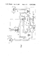
- FIG. 1 is a CCD system incorporating a preferred embodiment of an image inspection system reduced to practice using hardware.
- FIG. 2 is a flow chart of a preferred embodiment of an image inspection system reduced to practice using software.
- FIG. 1 shows a system including a charge coupled device (CCD) 11 for inspecting an image source 10.
- the object being inspected can be another CCD, a light image, a high resolution cathode ray tube (CRT) or other type of image source.
- the light rays 10a eminating from the image source 10 impinge upon the CCD and each pixel of the CCD is charged proportionately to the amount of light energy received.
- a data transfer and address generator 12 is coupled to the CCD 11 by output lines 13.
- the data transfer and address generator 12 controls the transfer of the analog information from the CCD to an image inspection system 14 through output circuitry 15.
- the transfer of the data from the CCD can be effected in a manner described in U.S. Pat. No. 4,454,545, or in any other manner within the purview of one skilled in the art.
- the data transfer and address generator 12 communicates with a variable frame store 16 and a reference frame store 17 through connecting lines 18 and 19, respectively.
- the reference frame store 17 also communicates with a digital processor 21 through the connection 22.
- the digital processor 21 can be a PROM, EPROM or RAM depending upon the flexibility and speed required for the particular inspection being performed.
- the variable frame store 16 also is coupled to the image source 10 by a line 23. In operation, the image source 10 generates or otherwise provides a light image which is projected onto the CCD 11 to charge each pixel within the CCD array proportionately to the amount of impinging light.
- the analog data on the CCD are read out to the output circuitry 15 and converted to digital information representative of the light image provided by the image source 10.
- the digital image data are then processed by the image inspection system 14 to either inspect or modify the image projected onto the CCD 11 by the image source 10.
- the output circuitry 15 communicates with the variable frame store 16 by way of a connection 24.
- the data transfer and address generator 12 transfers the analog data from the CCD 11 to the output circuitry 15, the data addresses for the variable frame store 15 and reference frame store 17 are communicated by way of connections 18 and 19 respectively. Accordingly, the data transferred from the CCD and the reference data are addressed so that the image data from the CCD can be compared with the reference data from the reference frame store 16 on a pixel by pixel basis.
- the image source 10 is a high resolution light source the output of which is variable on a pixel by pixel basis. Thus the image source 10 can be a high resolution CRT which is used to generate any desired image.
- the present system also is useful in inspecting production type CCDs.
- the image source 10 generates a white field and an optimum, or reference, CCD is used as the CCD 11.
- the white field from the image source 10 is projected onto the reference CCD to provide reference field data to the reference frame store 17.
- the reference field data can be provided by the digital processor 21 because the optimum output data from an optimum CCD are known.
- the reference CCD data are stored in the reference frame store 17, the reference CCD is replaced by a production CCD without changing the white field provided by the image source 10.
- the production CCD is then exposed to the white field and the data provided to the variable frame store 16.
- the data from the reference CCD and the production CCD are respectively addressed to the reference frame store 17 and the variable frame store 16, and the image data from the production CCD can be compared with the reference data from the optimum CCD on a pixel by pixel basis.
- a pixel by pixel comparison of the production CCD with the reference CCD data identifies the pixel locations of all faults within the production CCD.
- the system is also useful for creating complex transmission patterns on regular photographic film.
- a photographic aperture having a two dimensional Gaussian transmission gradient rather than the typical circular aperture is needed.
- Such a Gaussian transmission aperture can be generated using the inventive system.
- the digital processor 21 is used to generate a digital picture of the desired transmission pattern and to load the data representive of the desired pattern into the reference frame store 17.
- the same digitized pattern is fed to the image source 10 to provide a best effort at generating the desired pattern.
- the best effort pattern is imaged onto a CCD and the image data from the CCD 11 are then compared with the reference data in the frame store 17.
- the differences between the data from the CCD 11 and the reference frame 17 are then provided to the variable frame store 16 on a pixel by pixel basis.
- the modified data in the variable frame store 16 are then provided over the coupling 23 to modify the image output from the image source 10.
- the modified image from the image source 10 is again projected onto the CCD and compared with the reference data in the reference frame store 17. This operation continues until the image received by the CCD 11 from the image source 10 is identical to that within the reference frame store 17 at which point the desired Gaussian transmission gradiant is provided by the image source 10.
- the CCD 11 is then replaced with a film camera and exposed to the light source to produce the desired Gaussian aperture on the photographic film.
- the image inspection system 14 includes a difference circuit 26 which receives the digitized pixel data from the output circuit 15 by way of a coupling 25.
- the difference circuit 26 also receives the reference pixel signals from the reference frame store 17 over the coupling 27.
- the difference circuit 26 compares the pixel data from the CCD with the reference pixel signals from the reference frame store 17 on a pixel by pixel basis to provide difference signals on the output lines 28 and 29.
- the output line 28 of the difference circuit 26 serves to provide the difference signals at an input to an adder means 31.
- the adder means 31 bilaterally communicates with the variable frame store 16 by way of the couplings 32 and 33.
- the difference signals on the output coupling 29 of the difference circuit 26 serves as an input to a comparator 34 which also receives a threshold value from the threshold select circuit 36.
- the pixels of the CCD are arranged in horizontal rows and vertical columns. During the transfer of data from the CCD, the data available on the individual pixels are read out serially from one horizontal row. When the row is empty the complete data field is shifted vertically one row to permit the serial removal of the next row from the CCD. This operation continues until all the pixel data is transferred from the CCD to the output circuitry 17.
- the data transfer and address generator 12 simultaneously addresses the variable frame store 16 and the reference frame store 17. Accordingly, when the pixel data from one pixel is received by the output circuitry 17 the pixel data is provided by the line 27 to the difference circuit 26.
- the reference pixel signal from the reference frame store 17 is provided to the difference circuit 26 to provide the difference signal for the particular pixel being investigated to the adder 31.
- the pixel data from the output circuitry 15 is provided to the variable frame store 16. This pixel data signal is provided by the variable frame store 16 over output line 32 to the adder 31.
- the pixel data and the difference signal are added by the adder 31 and provided by the output circuitry to the variable frame store 16 so that the pixel data is replaced by the modified pixel signal which results from the addition of the pixel data in the pixel difference signal.
- This operation continues on a pixel by pixel basis until all the pixel data signals are scanned from the CCD 11 and modified in the variable frame store 16.
- the modified signals in the frame store 16 can then be used to modify the image provided by the image source 10 or used as an indication of the quality of the CCD 11 from which the data have been received.
- the image inspection system 14 can also be used to immediately reject an image being investigated.
- the difference signal from the difference circuit 26 is provided by the output line 29 to the comparator 34.
- a threshold select switch 36 provides a threshold value for the difference signal and provides the threshold value to the comparator 34 by way of the output line 37. Some variations in the image intensity are permitted and the threshold value is selected to permit the allowable variation by comparing the difference signals from the difference circuit 26 with the permitted threshold value from the threshold select switch 36.
- the difference signal is different from the threshold value by less than a preselected maximum an acceptable image has been received.
- an unacceptable pixel has been detected in the image projected onto the CCD 11 and a flag signal is provided on the output line 38 of the comparator 34.
- FIG. 2 is a flow chart of a preferred embodiment when the image inspection system 14 of FIG. 1 is reduced to practice utilizing software.
- the digital processor 21 of FIG. 1 has sufficient memory capacity all the elements contain within the image inspection system 14 of FIG. 1 can be replaced by properly programming the digital processor.
- the routine is entered at the start function 41 and as indicated at function 42 the variable frame store and address generator are cleared.
- the reference frame is loaded into the frame store.
- the CCD is exposed to the image and the output digitized and stored as indicated at functional block 44.
- one pixel of the variable frame store and the reference frame store are simultaneously accessed to provide the difference signal as indicated at functional block 46.
- the difference signal is compared with the threshold level and if the difference signal exceeds the threshold by more than a predetermined maximum the flag is set as indicated at functional block 48.
- functional block 49 is entered to provide the modified signal to the variable frame store. The next pixel is then addressed at functional block 50. This operation continues until the complete CCD is scanned as indicated at functional block 51.
- decision block 52 is entered and when a flag is set because a difference signal exceeds the threshold value functional block 53 is entered to reset the address generator and repeat the inspection of the image to verify that the flag indication did not result from an erroneous inspection.
- the routine is ended as indicated at 54.
Abstract
Description
Claims (15)
Priority Applications (1)
| Application Number | Priority Date | Filing Date | Title |
|---|---|---|---|
| US06/388,037 US4542404A (en) | 1982-06-14 | 1982-06-14 | Charge coupled device based system and method for inspecting and modifying images |
Applications Claiming Priority (1)
| Application Number | Priority Date | Filing Date | Title |
|---|---|---|---|
| US06/388,037 US4542404A (en) | 1982-06-14 | 1982-06-14 | Charge coupled device based system and method for inspecting and modifying images |
Related Child Applications (1)
| Application Number | Title | Priority Date | Filing Date |
|---|---|---|---|
| US06/533,883 Continuation US4500589A (en) | 1981-01-09 | 1983-09-20 | Laminate of aluminum sheet material and aramid fibers |
Publications (1)
| Publication Number | Publication Date |
|---|---|
| US4542404A true US4542404A (en) | 1985-09-17 |
Family
ID=23532377
Family Applications (1)
| Application Number | Title | Priority Date | Filing Date |
|---|---|---|---|
| US06/388,037 Expired - Fee Related US4542404A (en) | 1982-06-14 | 1982-06-14 | Charge coupled device based system and method for inspecting and modifying images |
Country Status (1)
| Country | Link |
|---|---|
| US (1) | US4542404A (en) |
Cited By (12)
| Publication number | Priority date | Publication date | Assignee | Title |
|---|---|---|---|---|
| US4641353A (en) * | 1983-09-16 | 1987-02-03 | Fujitsu Limited | Inspection method and apparatus for a mask pattern used in semiconductor device fabrication |
| US4675729A (en) * | 1986-06-13 | 1987-06-23 | Rca Corporation | Method of detecting blemishes in the phosphor screen on a kinescope faceplate |
| US4771468A (en) * | 1986-04-17 | 1988-09-13 | International Business Machines Corporation | System for automatic inspection of periodic patterns |
| US4908702A (en) * | 1988-04-29 | 1990-03-13 | The United States Of America As Represented By The Administrator Of The National Aeronautics And Space Administration | Real-time image difference detection using a polarization rotation spacial light modulator |
| US4949390A (en) * | 1987-04-16 | 1990-08-14 | Applied Vision Systems, Inc. | Interconnect verification using serial neighborhood processors |
| US4985847A (en) * | 1987-01-14 | 1991-01-15 | Hitachi, Ltd. | Visual sensor system |
| US5293543A (en) * | 1991-02-13 | 1994-03-08 | Kabushiki Kaisha Toshiba | Apparatus for color imager defect determination |
| US5387932A (en) * | 1991-07-06 | 1995-02-07 | Sony Corporation | Video camera capable of adding, transmitting, and extracting a reference signal indicative of the position of a reference pixel |
| US5515102A (en) * | 1993-03-09 | 1996-05-07 | Hughes Aircraft Company | Charge coupled device apparatus having means for correcting for changes in the charge transfer efficiency of a charge coupled device |
| US5928821A (en) * | 1995-12-22 | 1999-07-27 | Thomson Consumer Electronics, Inc. | Method of manufacturing a phosphor screen for a CRT |
| US6178257B1 (en) * | 1990-11-16 | 2001-01-23 | Applied Materials, Inc. | Substrate inspection method and apparatus |
| US20050008218A1 (en) * | 1998-07-15 | 2005-01-13 | O'dell Jeffrey | Automated wafer defect inspection system and a process of performing such inspection |
Citations (5)
| Publication number | Priority date | Publication date | Assignee | Title |
|---|---|---|---|---|
| US4164728A (en) * | 1976-12-11 | 1979-08-14 | Emi Limited | Correlation techniques |
| US4319221A (en) * | 1979-05-29 | 1982-03-09 | Nippon Electric Co., Ltd. | Similarity calculator comprising a buffer for a single input pattern feature vector to be pattern matched with reference patterns |
| US4378495A (en) * | 1980-11-07 | 1983-03-29 | Owens-Illinois, Inc. | Method and apparatus for setup of inspection devices for glass bottles |
| US4398213A (en) * | 1980-05-12 | 1983-08-09 | Siemens Aktiengesellschaft | X-Ray diagnostic installation for providing subtraction images |
| US4448532A (en) * | 1981-03-31 | 1984-05-15 | Kla Instruments Corporation | Automatic photomask inspection method and system |
-
1982
- 1982-06-14 US US06/388,037 patent/US4542404A/en not_active Expired - Fee Related
Patent Citations (5)
| Publication number | Priority date | Publication date | Assignee | Title |
|---|---|---|---|---|
| US4164728A (en) * | 1976-12-11 | 1979-08-14 | Emi Limited | Correlation techniques |
| US4319221A (en) * | 1979-05-29 | 1982-03-09 | Nippon Electric Co., Ltd. | Similarity calculator comprising a buffer for a single input pattern feature vector to be pattern matched with reference patterns |
| US4398213A (en) * | 1980-05-12 | 1983-08-09 | Siemens Aktiengesellschaft | X-Ray diagnostic installation for providing subtraction images |
| US4378495A (en) * | 1980-11-07 | 1983-03-29 | Owens-Illinois, Inc. | Method and apparatus for setup of inspection devices for glass bottles |
| US4448532A (en) * | 1981-03-31 | 1984-05-15 | Kla Instruments Corporation | Automatic photomask inspection method and system |
Cited By (20)
| Publication number | Priority date | Publication date | Assignee | Title |
|---|---|---|---|---|
| US4641353A (en) * | 1983-09-16 | 1987-02-03 | Fujitsu Limited | Inspection method and apparatus for a mask pattern used in semiconductor device fabrication |
| US4771468A (en) * | 1986-04-17 | 1988-09-13 | International Business Machines Corporation | System for automatic inspection of periodic patterns |
| US4675729A (en) * | 1986-06-13 | 1987-06-23 | Rca Corporation | Method of detecting blemishes in the phosphor screen on a kinescope faceplate |
| US4985847A (en) * | 1987-01-14 | 1991-01-15 | Hitachi, Ltd. | Visual sensor system |
| US4949390A (en) * | 1987-04-16 | 1990-08-14 | Applied Vision Systems, Inc. | Interconnect verification using serial neighborhood processors |
| US4908702A (en) * | 1988-04-29 | 1990-03-13 | The United States Of America As Represented By The Administrator Of The National Aeronautics And Space Administration | Real-time image difference detection using a polarization rotation spacial light modulator |
| US6178257B1 (en) * | 1990-11-16 | 2001-01-23 | Applied Materials, Inc. | Substrate inspection method and apparatus |
| US7499583B2 (en) | 1990-11-16 | 2009-03-03 | Applied Materials, Israel, Ltd. | Optical inspection method for substrate defect detection |
| US20020039436A1 (en) * | 1990-11-16 | 2002-04-04 | David Alumot | Optical inspection apparatus for defect detection |
| US20040218807A1 (en) * | 1990-11-16 | 2004-11-04 | Applied Materials, Inc. | Optical inspection method for substrate defect detection |
| US6952491B2 (en) | 1990-11-16 | 2005-10-04 | Applied Materials, Inc. | Optical inspection apparatus for substrate defect detection |
| US5293543A (en) * | 1991-02-13 | 1994-03-08 | Kabushiki Kaisha Toshiba | Apparatus for color imager defect determination |
| US5387932A (en) * | 1991-07-06 | 1995-02-07 | Sony Corporation | Video camera capable of adding, transmitting, and extracting a reference signal indicative of the position of a reference pixel |
| US5515102A (en) * | 1993-03-09 | 1996-05-07 | Hughes Aircraft Company | Charge coupled device apparatus having means for correcting for changes in the charge transfer efficiency of a charge coupled device |
| US5928821A (en) * | 1995-12-22 | 1999-07-27 | Thomson Consumer Electronics, Inc. | Method of manufacturing a phosphor screen for a CRT |
| US20050008218A1 (en) * | 1998-07-15 | 2005-01-13 | O'dell Jeffrey | Automated wafer defect inspection system and a process of performing such inspection |
| US7729528B2 (en) | 1998-07-15 | 2010-06-01 | Rudolph Technologies, Inc. | Automated wafer defect inspection system and a process of performing such inspection |
| US20100239157A1 (en) * | 1998-07-15 | 2010-09-23 | Rudolph Technologies, Inc. | Automated wafer defect inspection system and a process of performing such inspection |
| US9337071B2 (en) | 1998-07-15 | 2016-05-10 | Rudolph Technologies, Inc. | Automated wafer defect inspection system and a process of performing such inspection |
| US9464992B2 (en) | 1998-07-15 | 2016-10-11 | Rudolph Technologies, Inc. | Automated wafer defect inspection system and a process of performing such inspection |
Similar Documents
| Publication | Publication Date | Title |
|---|---|---|
| US4454541A (en) | Charge coupled device based blemish detection system and method | |
| US4542404A (en) | Charge coupled device based system and method for inspecting and modifying images | |
| US5361140A (en) | Method and apparatus for dynamic correction of microscopic image signals | |
| CA1119716A (en) | Blemish compensating system for a solid state image pick-up device | |
| CN101778222B (en) | Image processing apparatus | |
| US7103208B2 (en) | Detecting and classifying blemishes on the transmissive surface of an image sensor package | |
| CA2053176A1 (en) | Method of and apparatus for inspecting bottle or the like | |
| US4454545A (en) | Charge coupled device based inspection system and method | |
| US6335757B1 (en) | CCD imaging device for high speed profiling | |
| EP1067777B1 (en) | Image sensing device, image processing apparatus and method, and memory medium | |
| US4314279A (en) | Matrix array camera | |
| US7936948B2 (en) | System and method for merging differently focused images | |
| US4484230A (en) | Image reproduction method and apparatus | |
| US4480264A (en) | Charge coupled device based system and method for measuring projected figures | |
| US5058183A (en) | Real video time size selection mode | |
| US5617223A (en) | Image scanner system and method for improved microfilm image quality | |
| US5245424A (en) | Defect detection method | |
| US4730213A (en) | Method measuring transparent elements and an opaque medium | |
| EP0442685A1 (en) | Method and system for measurement of characteristics of image display | |
| JPH0759011A (en) | Automatic detector and automatic correction device for defective picture element on solid-state image pickup element | |
| US4805124A (en) | System and method for measuring elliptical elements | |
| EP0474762B1 (en) | Method and apparatus for correcting shading effects in video images | |
| US4750210A (en) | Method and apparatus for finding objects within a visual display | |
| JPH0435466A (en) | Picture signal processor | |
| JPH08202871A (en) | Picture information processor |
Legal Events
| Date | Code | Title | Description |
|---|---|---|---|
| AS | Assignment |
Owner name: RCA CORPORATION, A CORP. OF DE. Free format text: ASSIGNMENT OF ASSIGNORS INTEREST.;ASSIGNOR:DUSCHL, ROBERT A.;REEL/FRAME:004006/0999 Effective date: 19820609 Owner name: RCA CORPORATION, A CORP. OF DE., STATELESS Free format text: ASSIGNMENT OF ASSIGNORS INTEREST;ASSIGNOR:DUSCHL, ROBERT A.;REEL/FRAME:004006/0999 Effective date: 19820609 |
|
| AS | Assignment |
Owner name: RCA LICENSING CORPORATION, TWO INDEPENDENCE WAY, P Free format text: ASSIGNMENT OF ASSIGNORS INTEREST.;ASSIGNOR:RCA CORPORATION, A CORP. OF DE;REEL/FRAME:004993/0131 Effective date: 19871208 |
|
| FPAY | Fee payment |
Year of fee payment: 4 |
|
| FPAY | Fee payment |
Year of fee payment: 8 |
|
| REMI | Maintenance fee reminder mailed | ||
| LAPS | Lapse for failure to pay maintenance fees | ||
| FP | Lapsed due to failure to pay maintenance fee |
Effective date: 19970917 |
|
| STCH | Information on status: patent discontinuation |
Free format text: PATENT EXPIRED DUE TO NONPAYMENT OF MAINTENANCE FEES UNDER 37 CFR 1.362 |