US4686386A - Power-down circuits for dynamic MOS integrated circuits - Google Patents
Power-down circuits for dynamic MOS integrated circuits Download PDFInfo
- Publication number
- US4686386A US4686386A US06/712,753 US71275385A US4686386A US 4686386 A US4686386 A US 4686386A US 71275385 A US71275385 A US 71275385A US 4686386 A US4686386 A US 4686386A
- Authority
- US
- United States
- Prior art keywords
- signal
- circuit
- clock
- clock signal
- pair
- Prior art date
- Legal status (The legal status is an assumption and is not a legal conclusion. Google has not performed a legal analysis and makes no representation as to the accuracy of the status listed.)
- Expired - Lifetime
Links
Images


Classifications
-
- G—PHYSICS
- G06—COMPUTING; CALCULATING OR COUNTING
- G06F—ELECTRIC DIGITAL DATA PROCESSING
- G06F1/00—Details not covered by groups G06F3/00 - G06F13/00 and G06F21/00
- G06F1/26—Power supply means, e.g. regulation thereof
- G06F1/32—Means for saving power
- G06F1/3203—Power management, i.e. event-based initiation of a power-saving mode
- G06F1/3234—Power saving characterised by the action undertaken
- G06F1/324—Power saving characterised by the action undertaken by lowering clock frequency
-
- G—PHYSICS
- G06—COMPUTING; CALCULATING OR COUNTING
- G06F—ELECTRIC DIGITAL DATA PROCESSING
- G06F1/00—Details not covered by groups G06F3/00 - G06F13/00 and G06F21/00
- G06F1/26—Power supply means, e.g. regulation thereof
- G06F1/32—Means for saving power
- G06F1/3203—Power management, i.e. event-based initiation of a power-saving mode
-
- H—ELECTRICITY
- H03—ELECTRONIC CIRCUITRY
- H03K—PULSE TECHNIQUE
- H03K5/00—Manipulating of pulses not covered by one of the other main groups of this subclass
- H03K5/15—Arrangements in which pulses are delivered at different times at several outputs, i.e. pulse distributors
- H03K5/15013—Arrangements in which pulses are delivered at different times at several outputs, i.e. pulse distributors with more than two outputs
-
- Y—GENERAL TAGGING OF NEW TECHNOLOGICAL DEVELOPMENTS; GENERAL TAGGING OF CROSS-SECTIONAL TECHNOLOGIES SPANNING OVER SEVERAL SECTIONS OF THE IPC; TECHNICAL SUBJECTS COVERED BY FORMER USPC CROSS-REFERENCE ART COLLECTIONS [XRACs] AND DIGESTS
- Y02—TECHNOLOGIES OR APPLICATIONS FOR MITIGATION OR ADAPTATION AGAINST CLIMATE CHANGE
- Y02D—CLIMATE CHANGE MITIGATION TECHNOLOGIES IN INFORMATION AND COMMUNICATION TECHNOLOGIES [ICT], I.E. INFORMATION AND COMMUNICATION TECHNOLOGIES AIMING AT THE REDUCTION OF THEIR OWN ENERGY USE
- Y02D10/00—Energy efficient computing, e.g. low power processors, power management or thermal management
Definitions
- This invention relates to a power-down circuit for dynamic MOS integrated circuits.
- Dynamic or clocked circuits have been widely used in MOS integrated circuits.
- the chief advantages of dynamic logic are as follows: (1) The flip-flop can be formed with fewer MOS devices. (2) System timing problems are simplified. (3) Less chip area is required per logic function, resulting in a lower cost of per function. (4) Since power is dissipated only when the load device is on, the power consumption is lower.
- the present invention provides a power-down circuit for reducing the operational power consumption of a dynamic MOS integrated circuit during idling conditions and comprising: a clock divider for generating a divided clock signal in response to an internal clock signal inputted thereto while receiving a control signal; the divided clock signal is synchronized with the internal clock signal and has a repetition rate which is slower than that of the internal clock signal; a control circuit for delivering the control signal when a triggering signal is inputted thereto; and a clock selecting circuit for transferring either the internal clock signal or the divided clock signal to the dynamic MOS integrated circuit in response to the control signal.
- the present invention also provides a power-down circuit for reducing the operational power consumption of a dynamic MOS integrated circuit during idling conditions and comprising: a clock divider for generating a divided clock signal in response to an internal clock signal inputted thereto while receiving a control signal; the divided clock signal is synchronized with the internal clock signal and has a repetition rate which is slower than that of the internal clock signal; a control circuit for delivering the control signal when a triggering signal is inputted thereto; and a clock selecting circuit for converting the divided clock signal into a first pair of clock signals and the internal clock signal into a second pair of clock signals, and for selectively delivering to the dynamic MOS integrated circuit either the first pair of clock signals or the second pair of clock signals in response to the control signal, the first pair of clock signals being nonoverlapping with respect to each other, the second pair of clock signals being nonoverlapping with respect to each other.
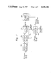
- FIG. 1 is a basic block diagram of a power-down circuit according to this invention used with a dynamic MOS logic circuit
- FIG. 2 is a circuit diagram of a power-down circuit according to this invention used with a dynamic MOS microprocessor
- FIG. 3 shows timing signals at various nodes of the power-down circuit of FIG. 2.
- FIG. 1 shows a MOS integrated circuit which has a basic power-down circuit according to this invention.
- the MOS integrated circuit includes an internal clock generator 100 for generating internal clock signals ( ⁇ I ) in response to an external clock signal ( ⁇ E ), an internal dynamic MOS logic circuit 102 for executing instructions, and a power-down circuit 104 for reducing the power consumption of the internal logic circuit 102.
- the power-down circuit 104 includes an internal clock divider 106 for dividing internal clock signals ( ⁇ I ) by 1/N, a control circuit 108 for generating a control signal (S C ) in response to an internal triggering signal (S I ) or an external triggering signal (S E ), and a clock selecting circuit 110 for selectively transferring either the clock signal ( ⁇ I ) or the divided clock signal ( ⁇ D ) to the dynamic logic circuit 102.
- the control circuit 108 does not send any control signal (S c ) to the clock divider 106 and to the clock selecting circuit 110.
- the clock selecting circuit 110 directly delivers the internal clock signal ( ⁇ I ) from the clock generator 100, so that the dynamic circuit 102 performs a normal logic operation.
- the logic circuit 102 outputs the triggering signal (S I ).
- the control circuit 108 ouputs the control signal (S C ) both to the clock divider 106 and to the clock selecting circuit 110.
- the clock divider 106 starts its clock pulse counting operation to output divided clock signals ( ⁇ D ).
- the clock selecting circuit 110 transfers the divided clock signal ( ⁇ D ) to the logic circuit 102, while it stops the internal clock signal ( ⁇ I ) from passing therethrough.
- the logic circuit 102 is operated with the divided clock signal ( ⁇ D ) during the idling conditions thereof.
- the MOS logic circuit 102 operates with a clock signal having a repetition rate which is slower than that of the internal clock signal ( ⁇ D ), the operational power dissipation can be reduced to a fraction of that needed during normal operation.
- FIG. 2 shows a MOS dynamic microprocessor having a power-down circuit according to this invention.
- the MOS dynamic microprocessor includes an internal clock generator 200 which generates internal clock signals ( ⁇ I ) when an external clock signal ( ⁇ E ) is inputted to terminal 276, an internal microprocessor 202 which executes instructions, and a power-down circuit 204 which reduces the power dissipation of the internal microprocessor 202.
- the power-down circuit 204 includes an internal clock divider 206 which divides internal clock signals ( ⁇ I ) to generate a divided clock signal ( ⁇ D ) while a control signal (S C ) is inputted thereto, a control circuit 208 which generates a control signal (S C ) in response to an internal triggering signal (S I ) or an external triggering signal (S E ), and a clock selecting circuit 210 which converts either the divided clock signal ( ⁇ D ) into a first pair of clock signals ( ⁇ x1, ⁇ x2) or the internal clock signal ( ⁇ I ) into a second pair of clock signals ( ⁇ y1, ⁇ y2), and which selectively transfers to the microprocessor 202 either the first pair of clock signals ( ⁇ x1, ⁇ x2) or the second pair of clock signals ( ⁇ y1, ⁇ y2) in response to the control signal (S.sub. C).
- an internal clock divider 206 which divides internal clock signals ( ⁇ I ) to generate a divided clock signal ( ⁇ D ) while a control signal (S C ) is
- the clock divider 206 for example, functions as a divide-by-4 counter, and comprises T-type flip-flops 210 and 212, an AND logic circuit 214, and an NOR logic circuit 216.
- the T-type flip-flop 210 has a clock terminal C for receiving the internal clock signal ( ⁇ I ) and a reset terminal R for receiving the control signal (S C ).
- the NOR logic circuit 216 outputs the divided clock signal ( ⁇ D ).
- the clock selecting circuit 210 comprises a first converter 218 which converts the divided clock signal ( ⁇ D ) into the first pair of clock signals ( ⁇ x1, ⁇ x2), a second converter 220 which converts the internal clock signal ( ⁇ I ) into the second pair of clock signals ( ⁇ y1, ⁇ y2), and a switching circuit 222 which selectively transfers either the first pair of clock signals ( ⁇ x1, ⁇ x2) or the second pair of clock signals ( ⁇ y1, ⁇ y2) to the microprocessor 202 in response to the control signal (S C ).
- the first and second converters 218 and 220 are formed of NAND logic circuits 224 and 226 and inverters 228, 230, 232, 234 and 236, respectively.
- the inverters 230 and 232 have time delay characteristics.
- the switching circuit 222 is formed of AND logic circuits 238, 240, 242 and 244, OR logic circuits 246 and 248, and inverters 250 and 252, respectively.
- Each of the converters 218 and 220 produces two clock signals which do no simultaneously have a "high level" so as to prevent overlapping conditions.
- the control circuit 208 comprises NOR logic circuits 262, 264, 266 and 268, AND logic circuits 254, 256, 258 and 260, an inverter 263, and an OR logic circuit 270.
- the NOR logic circuit 268 delivers the control signal (S C ) to the clock divider 206 and to the switching circuit 210.
- the OR logic circuit 270 receives a triggering signal (S I ) from the microprocessor 202.
- a triggering signal (S E ) may also be externally inputted by way of a terminal 274.
- the clock signal ( ⁇ y1) from the second converter 220 is sent to the control circuit 208 to synchronize a releasing signal (R E ) or the triggering signal (S I ) with the clock signal ( ⁇ I ).
- the releasing signal (R E ) is received by the control circuit 208 to release an idling condition of the microprocessor 202 under the power-down mode.
- an external clock signal ( ⁇ E ) is applied to the terminal 276, and the terminals 272 and 274 are at an "L" level, respectively.
- the control circuit 208 does not deliver the control signal (S C ), so that the clock divider 206 ceases its dividing operation, while the switching circuit 222 selects the second converter 220.
- the second converter 220 receives the internal clock signal ( ⁇ I ) from the clock generator 200 to deliver the second pair of clock signals ( ⁇ y1, ⁇ y2) to the switching circuit 222, as shown in FIG. 3.
- These signals ( ⁇ y1, ⁇ y2) are sent as two-phase clock signals to the microprocessor 202 by way of the switching circuit 222, as shown in FIG. 3 (F). Therefore, the microprocessor 202 operates in accordance with the pair of clock signals ( ⁇ y1, ⁇ y2).
- the microprocessor 202 when the microprocessor 202 executes a completion of a "HOLD" instruction, it delivers an internal triggering signal (S I ), as shown in FIG. 3 (I).
- the triggering signal (S I ) is applied to the control circuit 208 in synchronization with the second clock signal ( ⁇ y1).
- the control circuit 208 outputs a control signal (S C ) of an "H” level, so that the clock divider 206 starts its counting operation of the clock signal ( ⁇ I), while the switching circuit 222 selects the first converter 218. Therefore, the switching circuit 222 delivers to the microprocessor 202 two clock signals ( ⁇ x1, ⁇ x2), each having a repetition rate which is slower than that of the internal clock signal ( ⁇ I ).
- the power dissipation of the microprocessor 202 is decreased to one fourth of that of normal operation during its power-down state.
- an external releasing signal (S E ) is applied to the terminal 272 as shown in FIG. 3 (H). Then, the output of the control circuit 208 becomes an "L" logic level in synchronization with the clock signal ( ⁇ y1), as shown in FIG. 3 (J).
- the clock divider 206 ceases the pulse counting operation, while the switching circuit 222 delivers the signals ( ⁇ y1, ⁇ y2) to the microprocessor 202.
- the power-down mode may be realized by externally applying an external triggering signal (S E ) to the terminal 274, as shown FIG. 3 (H).
- S E external triggering signal
- the frequency of the divided clock signal ( ⁇ D ) should be decreased to a value that the dynamic MOS logic circuit can hold information in clock (refresh) operations to save power consumption.
- the power-down circuit according to this invention can carry out a power-down mode without destroying stored information and without losing the advantages of the dynamic MOS logic circuit.
Abstract
A power-down circuit for saving operational power dissipation of a dynamic MOS integrated circuit during idling conditions. A clock divider generates a divided clock signal in response to an internal clock signal inputted thereto. The divided signal is synchronized with the internal clock signal and has a repetition rate which is slower than that of the internal clock signal. A control circuit delivers the control signal when a triggering signal is inputted thereto. A clock selecting circuit transfers either the internal clock signal or the divided clock signal to the dynamic MOS integrated circuit in response to the control signal.
Description
This invention relates to a power-down circuit for dynamic MOS integrated circuits.
Dynamic or clocked circuits have been widely used in MOS integrated circuits. The chief advantages of dynamic logic are as follows: (1) The flip-flop can be formed with fewer MOS devices. (2) System timing problems are simplified. (3) Less chip area is required per logic function, resulting in a lower cost of per function. (4) Since power is dissipated only when the load device is on, the power consumption is lower.
In case a MOS integrated circuit is powered with a battery, the use of a power-down circuit is useful to prolong the life of the battery. In static MOS logic integrated circuits, power saving can be easily realized by ceasing clock signals during idling conditions without destroying data stored therein. However, in the dynamic MOS logic integrated circuits, if clock signals are stopped during idling conditions, all the functions will cease, resulting in a loss of stored information. For this reason, it has been difficult to operate dynamic MOS integrated circuit in a power-down mode without occurring a loss of stored data.
It is therefore an object of the present invention to provide an improved power-down circuit for saving power consumption of a dynamic MOS integrated circuit.
It is another object of the present invention to provide a power-down circuit for dynamic MOS microprocessor integrated circuits.
The present invention provides a power-down circuit for reducing the operational power consumption of a dynamic MOS integrated circuit during idling conditions and comprising: a clock divider for generating a divided clock signal in response to an internal clock signal inputted thereto while receiving a control signal; the divided clock signal is synchronized with the internal clock signal and has a repetition rate which is slower than that of the internal clock signal; a control circuit for delivering the control signal when a triggering signal is inputted thereto; and a clock selecting circuit for transferring either the internal clock signal or the divided clock signal to the dynamic MOS integrated circuit in response to the control signal.
The present invention also provides a power-down circuit for reducing the operational power consumption of a dynamic MOS integrated circuit during idling conditions and comprising: a clock divider for generating a divided clock signal in response to an internal clock signal inputted thereto while receiving a control signal; the divided clock signal is synchronized with the internal clock signal and has a repetition rate which is slower than that of the internal clock signal; a control circuit for delivering the control signal when a triggering signal is inputted thereto; and a clock selecting circuit for converting the divided clock signal into a first pair of clock signals and the internal clock signal into a second pair of clock signals, and for selectively delivering to the dynamic MOS integrated circuit either the first pair of clock signals or the second pair of clock signals in response to the control signal, the first pair of clock signals being nonoverlapping with respect to each other, the second pair of clock signals being nonoverlapping with respect to each other.
The above and other objects, features and advantages of the present invention will become more apparent from the following description when taken in conjunction with the accompanying drawings in which a preferred embodiment of the present invention is shown by way of illustrative example.
In the accompanying drawings:
FIG. 1 is a basic block diagram of a power-down circuit according to this invention used with a dynamic MOS logic circuit;
FIG. 2 is a circuit diagram of a power-down circuit according to this invention used with a dynamic MOS microprocessor; and
FIG. 3 shows timing signals at various nodes of the power-down circuit of FIG. 2.
FIG. 1 shows a MOS integrated circuit which has a basic power-down circuit according to this invention. In FIG. 1, the MOS integrated circuit includes an internal clock generator 100 for generating internal clock signals (φI) in response to an external clock signal (φE), an internal dynamic MOS logic circuit 102 for executing instructions, and a power-down circuit 104 for reducing the power consumption of the internal logic circuit 102. The power-down circuit 104 includes an internal clock divider 106 for dividing internal clock signals (φI) by 1/N, a control circuit 108 for generating a control signal (SC) in response to an internal triggering signal (SI) or an external triggering signal (SE), and a clock selecting circuit 110 for selectively transferring either the clock signal (φI) or the divided clock signal (φD) to the dynamic logic circuit 102.
During normal operation, since the internal dynamic logic circuit 102 does not output an internal triggering signal (SI), the control circuit 108 does not send any control signal (Sc) to the clock divider 106 and to the clock selecting circuit 110. In this case, the clock selecting circuit 110 directly delivers the internal clock signal (φI) from the clock generator 100, so that the dynamic circuit 102 performs a normal logic operation.
During an idle condition, the logic circuit 102 outputs the triggering signal (SI). As a result, the control circuit 108 ouputs the control signal (SC) both to the clock divider 106 and to the clock selecting circuit 110. Then, the clock divider 106 starts its clock pulse counting operation to output divided clock signals (φD). The clock selecting circuit 110 transfers the divided clock signal (φD) to the logic circuit 102, while it stops the internal clock signal (φI) from passing therethrough. The logic circuit 102 is operated with the divided clock signal (φD) during the idling conditions thereof.
As described above, since the MOS logic circuit 102 operates with a clock signal having a repetition rate which is slower than that of the internal clock signal (φD), the operational power dissipation can be reduced to a fraction of that needed during normal operation.
FIG. 2 shows a MOS dynamic microprocessor having a power-down circuit according to this invention.
In FIG. 2, the MOS dynamic microprocessor includes an internal clock generator 200 which generates internal clock signals (φI) when an external clock signal (φE) is inputted to terminal 276, an internal microprocessor 202 which executes instructions, and a power-down circuit 204 which reduces the power dissipation of the internal microprocessor 202. The power-down circuit 204 includes an internal clock divider 206 which divides internal clock signals (φI) to generate a divided clock signal (φD) while a control signal (SC) is inputted thereto, a control circuit 208 which generates a control signal (SC) in response to an internal triggering signal (SI) or an external triggering signal (SE), and a clock selecting circuit 210 which converts either the divided clock signal (φD) into a first pair of clock signals (φx1,φx2) or the internal clock signal (φI) into a second pair of clock signals (φy1,φy2), and which selectively transfers to the microprocessor 202 either the first pair of clock signals (φx1,φx2) or the second pair of clock signals (φy1,φy2) in response to the control signal (S.sub. C).
The external clock signal (φE) from a crystal oscillator (not shown), for example, is applied to the terminal 276.
The clock divider 206 for example, functions as a divide-by-4 counter, and comprises T-type flip- flops 210 and 212, an AND logic circuit 214, and an NOR logic circuit 216. The T-type flip-flop 210 has a clock terminal C for receiving the internal clock signal (φI) and a reset terminal R for receiving the control signal (SC). The NOR logic circuit 216 outputs the divided clock signal (φD).
The clock selecting circuit 210 comprises a first converter 218 which converts the divided clock signal (φD) into the first pair of clock signals (φx1,φx2), a second converter 220 which converts the internal clock signal (φI) into the second pair of clock signals (φy1,φy2), and a switching circuit 222 which selectively transfers either the first pair of clock signals (φx1,φx2) or the second pair of clock signals (φy1,φy2) to the microprocessor 202 in response to the control signal (SC). The first and second converters 218 and 220 are formed of NAND logic circuits 224 and 226 and inverters 228, 230, 232, 234 and 236, respectively. The inverters 230 and 232 have time delay characteristics. The switching circuit 222 is formed of AND logic circuits 238, 240, 242 and 244, OR logic circuits 246 and 248, and inverters 250 and 252, respectively. Each of the converters 218 and 220 produces two clock signals which do no simultaneously have a "high level" so as to prevent overlapping conditions.
The control circuit 208 comprises NOR logic circuits 262, 264, 266 and 268, AND logic circuits 254, 256, 258 and 260, an inverter 263, and an OR logic circuit 270. The NOR logic circuit 268 delivers the control signal (SC) to the clock divider 206 and to the switching circuit 210. The OR logic circuit 270 receives a triggering signal (SI) from the microprocessor 202. A triggering signal (SE) may also be externally inputted by way of a terminal 274. The clock signal (φy1) from the second converter 220 is sent to the control circuit 208 to synchronize a releasing signal (RE) or the triggering signal (SI) with the clock signal (φI). The releasing signal (RE) is received by the control circuit 208 to release an idling condition of the microprocessor 202 under the power-down mode.
Next, the operation of the power-down circuit according to this invention will be described in reference to FIG. 3.
In operation, an external clock signal (φE) is applied to the terminal 276, and the terminals 272 and 274 are at an "L" level, respectively. In a normal condition, since the internal triggering signal (SI) is at an "L" level, the control circuit 208 does not deliver the control signal (SC), so that the clock divider 206 ceases its dividing operation, while the switching circuit 222 selects the second converter 220. The second converter 220 receives the internal clock signal (φI) from the clock generator 200 to deliver the second pair of clock signals (φy1, φy2) to the switching circuit 222, as shown in FIG. 3. These signals (φy1,φy2) are sent as two-phase clock signals to the microprocessor 202 by way of the switching circuit 222, as shown in FIG. 3 (F). Therefore, the microprocessor 202 operates in accordance with the pair of clock signals (φy1, φy2).
For example, when the microprocessor 202 executes a completion of a "HOLD" instruction, it delivers an internal triggering signal (SI), as shown in FIG. 3 (I). The triggering signal (SI) is applied to the control circuit 208 in synchronization with the second clock signal (φy1). The control circuit 208 outputs a control signal (SC) of an "H" level, so that the clock divider 206 starts its counting operation of the clock signal (φI), while the switching circuit 222 selects the first converter 218. Therefore, the switching circuit 222 delivers to the microprocessor 202 two clock signals (φx1,φx2), each having a repetition rate which is slower than that of the internal clock signal (φI). As a result, the power dissipation of the microprocessor 202 is decreased to one fourth of that of normal operation during its power-down state.
Next, in order to return to the normal condition, an external releasing signal (SE) is applied to the terminal 272 as shown in FIG. 3 (H). Then, the output of the control circuit 208 becomes an "L" logic level in synchronization with the clock signal (φy1), as shown in FIG. 3 (J). The clock divider 206 ceases the pulse counting operation, while the switching circuit 222 delivers the signals (φy1,φy2) to the microprocessor 202.
The power-down mode may be realized by externally applying an external triggering signal (SE) to the terminal 274, as shown FIG. 3 (H). The frequency of the divided clock signal (φD) should be decreased to a value that the dynamic MOS logic circuit can hold information in clock (refresh) operations to save power consumption.
As described above, the power-down circuit according to this invention can carry out a power-down mode without destroying stored information and without losing the advantages of the dynamic MOS logic circuit.
Claims (3)
1. A power-down circuit for reducing operational power consumption of a dynamic MOS integrated circuit during idling conditions, said power-down circuit comprising:
a clock divider for generating a divided clock signal in response to an internal clock signal inputted thereto while receiving a control signal, said divided clock signal being synchronized with said internal clock signal and having a repetition rate which is slower than that of said internal clock signal;
a control circuit for delivering said control signal when a triggering signal from said dynamic MOS integrated circuit or from an external triggering signal source is inputted thereto; and
a clock selecting circuit having a first input for receiving said divided clock signal, a second input for receiving said internal clock signal, a third input for receiving said control signal, and an output coupled to said dynamic MOS integrated circuit, for converting said divided clock signal into a first pair of clock signals and for converting said internal clock signal into a second pair of clock signals, and for selectively transferring to said dynamic MOS integrated circuit either said first pair of clock signals or said second pair of clock signals in response to said control signal, said first pair of clock signals being nonoverlapping with respect to each other and said second pair of clock signals being nonoverlapping with respect to each other.
2. A circuit according to claim 1, wherein said selecting circuit comprises a first converter for converting said divided clock signal into said first pair of clock signals, a second converter for converting said internal clock signal into said second pair of clock signals, a switching circuit for selectively transferring either said first pair of clock signals or said second pair of clock signals to said MOS integrated circuit in response to said control signal.
3. A circuit according to claim 2, wherein said dynamic MOS integrated circuit delivers said triggering signal in response to execution of instructions by said dynamic MOS integrated circuit.
Applications Claiming Priority (2)
| Application Number | Priority Date | Filing Date | Title |
|---|---|---|---|
| JP59-52372 | 1984-03-21 | ||
| JP59052372A JPS60198618A (en) | 1984-03-21 | 1984-03-21 | Dynamic logical circuit |
Publications (1)
| Publication Number | Publication Date |
|---|---|
| US4686386A true US4686386A (en) | 1987-08-11 |
Family
ID=12912970
Family Applications (1)
| Application Number | Title | Priority Date | Filing Date |
|---|---|---|---|
| US06/712,753 Expired - Lifetime US4686386A (en) | 1984-03-21 | 1985-03-18 | Power-down circuits for dynamic MOS integrated circuits |
Country Status (2)
| Country | Link |
|---|---|
| US (1) | US4686386A (en) |
| JP (1) | JPS60198618A (en) |
Cited By (78)
| Publication number | Priority date | Publication date | Assignee | Title |
|---|---|---|---|---|
| US4736119A (en) * | 1987-02-04 | 1988-04-05 | American Telephone And Telegraph Company, At&T Bell Laboratories | Dynamic CMOS current surge control |
| US4816700A (en) * | 1987-12-16 | 1989-03-28 | Intel Corporation | Two-phase non-overlapping clock generator |
| US4881205A (en) * | 1987-04-21 | 1989-11-14 | Casio Computer Co., Ltd. | Compact electronic apparatus with a refresh unit for a dynamic type memory |
| US4920282A (en) * | 1987-06-23 | 1990-04-24 | Kabushiki Kaisha Toshiba | Dynamic latch circuit for preventing short-circuit current from flowing during absence of clock pulses when under test |
| US4968900A (en) * | 1989-07-31 | 1990-11-06 | Harris Corporation | Programmable speed/power arrangement for integrated devices having logic matrices |
| EP0419908A2 (en) * | 1989-09-29 | 1991-04-03 | Kabushiki Kaisha Toshiba | Computer system with a sleep mode function |
| EP0426410A2 (en) * | 1989-10-30 | 1991-05-08 | Texas Instruments Incorporated | Real-time power conservation for portable computers |
| US5025387A (en) * | 1988-09-06 | 1991-06-18 | Motorola, Inc. | Power saving arrangement for a clocked digital circuit |
| US5083266A (en) * | 1986-12-26 | 1992-01-21 | Kabushiki Kaisha Toshiba | Microcomputer which enters sleep mode for a predetermined period of time on response to an activity of an input/output device |
| EP0474963A2 (en) * | 1990-09-13 | 1992-03-18 | Kabushiki Kaisha Toshiba | Computer system having sleep mode function |
| US5099140A (en) * | 1990-08-31 | 1992-03-24 | Advanced Micro Devices, Inc. | Synchronous clock source selector |
| WO1992007317A1 (en) * | 1990-10-12 | 1992-04-30 | Intel Corporation | Slow memory refresh in a computer with a limited supply of power |
| EP0486794A2 (en) * | 1990-10-23 | 1992-05-27 | International Business Machines Corporation | DRAM having extended refresh time |
| US5132932A (en) * | 1989-05-19 | 1992-07-21 | Mitsubishi Denki Kabushiki Kaisha | Dynamic random access memory having a plurality of rated voltages as operation supply voltage and operating method thereof |
| US5151855A (en) * | 1989-10-19 | 1992-09-29 | Saturn Corporation | Multiple microprocessor single power supply system shutdown |
| US5167031A (en) * | 1987-05-14 | 1992-11-24 | Sony Corporation | Variable frequency clock pulse generator for microcomputer |
| EP0522720A1 (en) * | 1991-06-18 | 1993-01-13 | Nokia Mobile Phones Ltd. | Clock frequency adjustment of an electrical circuit |
| US5272398A (en) * | 1991-09-12 | 1993-12-21 | Otis Elevator Company | Driver for power field-controlled switches with refreshed power supply providing stable on/off switching |
| US5300831A (en) * | 1992-09-04 | 1994-04-05 | Pham Dac C | Logic macro and protocol for reduced power consumption during idle state |
| US5343096A (en) * | 1992-05-19 | 1994-08-30 | Hewlett-Packard Company | System and method for tolerating dynamic circuit decay |
| US5365487A (en) * | 1992-03-24 | 1994-11-15 | Texas Instruments Incorporated | DRAM power management with self-refresh |
| US5379408A (en) * | 1991-11-08 | 1995-01-03 | Texas Instruments Incorporated | Color palette timing and control with circuitry for producing an additional clock cycle during a clock disabled time period |
| US5420808A (en) * | 1993-05-13 | 1995-05-30 | International Business Machines Corporation | Circuitry and method for reducing power consumption within an electronic circuit |
| EP0666527A1 (en) * | 1994-02-02 | 1995-08-09 | Advanced Micro Devices, Inc. | Power management unit for a computer system |
| US5442774A (en) * | 1993-09-16 | 1995-08-15 | Hewlett-Packard Company | Microprocessor controller with automatic clock-rate switching |
| US5475324A (en) * | 1992-03-11 | 1995-12-12 | Nec Corporation | Clock generator with an automatic frequency change function |
| US5502689A (en) * | 1992-07-21 | 1996-03-26 | Advanced Micro Devices, Inc. | Clock generator capable of shut-down mode and clock generation method |
| US5511209A (en) * | 1989-06-20 | 1996-04-23 | Mensch, Jr.; William D. | Programmable microcomputer oscillator circuitry with synchronized fast and slow clock output signal |
| US5587675A (en) * | 1993-08-12 | 1996-12-24 | At&T Global Information Solutions Company | Multiclock controller |
| US5587672A (en) * | 1995-09-25 | 1996-12-24 | Neomagic Corp. | Dynamic logic having power-down mode with periodic clock refresh for a low-power graphics controller |
| US5696729A (en) * | 1993-12-17 | 1997-12-09 | Nec Corporation | Power reducing circuit for synchronous semiconductor device |
| US5758134A (en) * | 1996-09-04 | 1998-05-26 | Radisys Corporation | Microprocessor embedded control system having an automatic clock slowdown circuit |
| US5774703A (en) * | 1996-01-05 | 1998-06-30 | Motorola, Inc. | Data processing system having a register controllable speed |
| US6031411A (en) * | 1993-06-28 | 2000-02-29 | Texas Instruments Incorporated | Low power substrate bias circuit |
| US6061418A (en) * | 1998-06-22 | 2000-05-09 | Xilinx, Inc. | Variable clock divider with selectable duty cycle |
| US6072348A (en) * | 1997-07-09 | 2000-06-06 | Xilinx, Inc. | Programmable power reduction in a clock-distribution circuit |
| US6094071A (en) * | 1999-03-15 | 2000-07-25 | International Business Machines Corporation | Initialization of floating body dynamic circuitry |
| US6153948A (en) * | 1998-08-13 | 2000-11-28 | Cogan; Adrian I. | Electronic circuits with wide dynamic range of on/off delay time |
| US6216235B1 (en) | 1994-06-20 | 2001-04-10 | C. Douglass Thomas | Thermal and power management for computer systems |
| US6259291B1 (en) * | 1998-11-27 | 2001-07-10 | Integrated Technology Express, Inc. | Self-adjusting apparatus and a self-adjusting method for adjusting an internal oscillating clock signal by using same |
| US6369643B1 (en) * | 1998-10-22 | 2002-04-09 | Lg Electronics Inc. | Apparatus and method for controlling power saving mode in a power supply |
| US6445228B1 (en) | 2001-08-28 | 2002-09-03 | Xilinx, Inc. | Programmable even-number clock divider circuit with duty cycle correction and optional phase shift |
| US6566918B1 (en) | 2001-08-28 | 2003-05-20 | Xilinx, Inc. | Divide-by-N clock divider circuit with minimal additional delay |
| US6593785B1 (en) | 1996-12-17 | 2003-07-15 | Cypress Semiconductor Corp. | Method and circuit for reducing power and/or current consumption |
| US6611158B2 (en) * | 2001-07-24 | 2003-08-26 | Koninklijke Philips Electronics N.V. | Method and system using a common reset and a slower reset clock |
| WO2003107152A2 (en) * | 2002-06-13 | 2003-12-24 | Sun Microsystems Inc. | Multiple supply voltage dynamic logic |
| US6714057B2 (en) | 2001-08-28 | 2004-03-30 | Xilinx, Inc. | Multi-purpose digital frequency synthesizer circuit for a programmable logic device |
| US6768362B1 (en) | 2001-08-13 | 2004-07-27 | Cypress Semiconductor Corp. | Fail-safe zero delay buffer with automatic internal reference |
| US20050223254A1 (en) * | 1989-10-30 | 2005-10-06 | Watts La Vaughn F Jr | Method for implementing thermal and power management in a processor and/or apparatus and/or system employing the same |
| US7093153B1 (en) * | 2002-10-30 | 2006-08-15 | Advanced Micro Devices, Inc. | Method and apparatus for lowering bus clock frequency in a complex integrated data processing system |
| US20070016816A1 (en) * | 2005-07-14 | 2007-01-18 | Toshihiko Himeno | Method and system for a clock circuit |
| US7167993B1 (en) | 1994-06-20 | 2007-01-23 | Thomas C Douglass | Thermal and power management for computer systems |
| US20070110142A1 (en) * | 2005-11-16 | 2007-05-17 | Cypress Semiconductor Corporation | Spread spectrum clock for USB |
| US20080215908A1 (en) * | 2005-05-10 | 2008-09-04 | Nxp B.V. | Sleep Watchdog Circuit For Asynchronous Digital Circuits |
| US7602214B2 (en) | 2002-09-06 | 2009-10-13 | Pact Xpp Technologies Ag | Reconfigurable sequencer structure |
| US7650448B2 (en) | 1996-12-20 | 2010-01-19 | Pact Xpp Technologies Ag | I/O and memory bus system for DFPS and units with two- or multi-dimensional programmable cell architectures |
| US7657877B2 (en) | 2001-06-20 | 2010-02-02 | Pact Xpp Technologies Ag | Method for processing data |
| US7822881B2 (en) | 1996-12-27 | 2010-10-26 | Martin Vorbach | Process for automatic dynamic reloading of data flow processors (DFPs) and units with two- or three-dimensional programmable cell architectures (FPGAs, DPGAs, and the like) |
| US7822968B2 (en) | 1996-12-09 | 2010-10-26 | Martin Vorbach | Circuit having a multidimensional structure of configurable cells that include multi-bit-wide inputs and outputs |
| US20100272811A1 (en) * | 2008-07-23 | 2010-10-28 | Alkermes,Inc. | Complex of trospium and pharmaceutical compositions thereof |
| US7840842B2 (en) | 2001-09-03 | 2010-11-23 | Martin Vorbach | Method for debugging reconfigurable architectures |
| US7844796B2 (en) | 2001-03-05 | 2010-11-30 | Martin Vorbach | Data processing device and method |
| US7996827B2 (en) | 2001-08-16 | 2011-08-09 | Martin Vorbach | Method for the translation of programs for reconfigurable architectures |
| US8058899B2 (en) | 2000-10-06 | 2011-11-15 | Martin Vorbach | Logic cell array and bus system |
| US8099618B2 (en) | 2001-03-05 | 2012-01-17 | Martin Vorbach | Methods and devices for treating and processing data |
| US8156284B2 (en) | 2002-08-07 | 2012-04-10 | Martin Vorbach | Data processing method and device |
| US8209653B2 (en) | 2001-09-03 | 2012-06-26 | Martin Vorbach | Router |
| US8250503B2 (en) | 2006-01-18 | 2012-08-21 | Martin Vorbach | Hardware definition method including determining whether to implement a function as hardware or software |
| US8281265B2 (en) | 2002-08-07 | 2012-10-02 | Martin Vorbach | Method and device for processing data |
| US8281108B2 (en) | 2002-01-19 | 2012-10-02 | Martin Vorbach | Reconfigurable general purpose processor having time restricted configurations |
| US8301872B2 (en) | 2000-06-13 | 2012-10-30 | Martin Vorbach | Pipeline configuration protocol and configuration unit communication |
| USRE44365E1 (en) | 1997-02-08 | 2013-07-09 | Martin Vorbach | Method of self-synchronization of configurable elements of a programmable module |
| US8686475B2 (en) | 2001-09-19 | 2014-04-01 | Pact Xpp Technologies Ag | Reconfigurable elements |
| US8686549B2 (en) | 2001-09-03 | 2014-04-01 | Martin Vorbach | Reconfigurable elements |
| US8812820B2 (en) | 2003-08-28 | 2014-08-19 | Pact Xpp Technologies Ag | Data processing device and method |
| US8819505B2 (en) | 1997-12-22 | 2014-08-26 | Pact Xpp Technologies Ag | Data processor having disabled cores |
| US8914590B2 (en) | 2002-08-07 | 2014-12-16 | Pact Xpp Technologies Ag | Data processing method and device |
| US9037807B2 (en) | 2001-03-05 | 2015-05-19 | Pact Xpp Technologies Ag | Processor arrangement on a chip including data processing, memory, and interface elements |
Families Citing this family (1)
| Publication number | Priority date | Publication date | Assignee | Title |
|---|---|---|---|---|
| JPH0267614A (en) * | 1988-09-01 | 1990-03-07 | Nec Ic Microcomput Syst Ltd | System clock circuit for microcomputer |
Citations (3)
| Publication number | Priority date | Publication date | Assignee | Title |
|---|---|---|---|---|
| US4137563A (en) * | 1976-06-30 | 1979-01-30 | Canon Kabushiki Kaisha | Circuitry for reducing power dissipation in equipment which operates in synchronism with clock pulses |
| US4293927A (en) * | 1979-12-12 | 1981-10-06 | Casio Computer Co., Ltd. | Power consumption control system for electronic digital data processing devices |
| US4317180A (en) * | 1979-12-26 | 1982-02-23 | Texas Instruments Incorporated | Clocked logic low power standby mode |
-
1984
- 1984-03-21 JP JP59052372A patent/JPS60198618A/en active Pending
-
1985
- 1985-03-18 US US06/712,753 patent/US4686386A/en not_active Expired - Lifetime
Patent Citations (3)
| Publication number | Priority date | Publication date | Assignee | Title |
|---|---|---|---|---|
| US4137563A (en) * | 1976-06-30 | 1979-01-30 | Canon Kabushiki Kaisha | Circuitry for reducing power dissipation in equipment which operates in synchronism with clock pulses |
| US4293927A (en) * | 1979-12-12 | 1981-10-06 | Casio Computer Co., Ltd. | Power consumption control system for electronic digital data processing devices |
| US4317180A (en) * | 1979-12-26 | 1982-02-23 | Texas Instruments Incorporated | Clocked logic low power standby mode |
Cited By (147)
| Publication number | Priority date | Publication date | Assignee | Title |
|---|---|---|---|---|
| US5083266A (en) * | 1986-12-26 | 1992-01-21 | Kabushiki Kaisha Toshiba | Microcomputer which enters sleep mode for a predetermined period of time on response to an activity of an input/output device |
| US4736119A (en) * | 1987-02-04 | 1988-04-05 | American Telephone And Telegraph Company, At&T Bell Laboratories | Dynamic CMOS current surge control |
| US4881205A (en) * | 1987-04-21 | 1989-11-14 | Casio Computer Co., Ltd. | Compact electronic apparatus with a refresh unit for a dynamic type memory |
| US5167031A (en) * | 1987-05-14 | 1992-11-24 | Sony Corporation | Variable frequency clock pulse generator for microcomputer |
| US4920282A (en) * | 1987-06-23 | 1990-04-24 | Kabushiki Kaisha Toshiba | Dynamic latch circuit for preventing short-circuit current from flowing during absence of clock pulses when under test |
| US4816700A (en) * | 1987-12-16 | 1989-03-28 | Intel Corporation | Two-phase non-overlapping clock generator |
| US5025387A (en) * | 1988-09-06 | 1991-06-18 | Motorola, Inc. | Power saving arrangement for a clocked digital circuit |
| US5132932A (en) * | 1989-05-19 | 1992-07-21 | Mitsubishi Denki Kabushiki Kaisha | Dynamic random access memory having a plurality of rated voltages as operation supply voltage and operating method thereof |
| US5418747A (en) * | 1989-05-19 | 1995-05-23 | Mitsubishi Denki Kabushiki Kaisha | Dynamic random access memory having a plurality of rated voltages as operation supply voltage and operating method thereof |
| US5315550A (en) * | 1989-05-19 | 1994-05-24 | Mitsubishi Denki Kabushiki Kaisha | Dynamic random access memory having sense amplifier activation delayed based on operation supply voltage and operating method thereof |
| US5511209A (en) * | 1989-06-20 | 1996-04-23 | Mensch, Jr.; William D. | Programmable microcomputer oscillator circuitry with synchronized fast and slow clock output signal |
| US4968900A (en) * | 1989-07-31 | 1990-11-06 | Harris Corporation | Programmable speed/power arrangement for integrated devices having logic matrices |
| EP0419908A2 (en) * | 1989-09-29 | 1991-04-03 | Kabushiki Kaisha Toshiba | Computer system with a sleep mode function |
| EP0419908A3 (en) * | 1989-09-29 | 1992-03-04 | Kabushiki Kaisha Toshiba | Computer system with a sleep mode function |
| US5151855A (en) * | 1989-10-19 | 1992-09-29 | Saturn Corporation | Multiple microprocessor single power supply system shutdown |
| US20050204178A1 (en) * | 1989-10-30 | 2005-09-15 | Watts Lavaughn F.Jr. | Method for controlling power consumption associated with a processor |
| US7284139B2 (en) | 1989-10-30 | 2007-10-16 | Texas Instruments Incorporated | Processor having real-time power conservation |
| US9021283B2 (en) | 1989-10-30 | 2015-04-28 | Texas Instruments Incorporated | Processor having real-time power conservation |
| US6633988B2 (en) | 1989-10-30 | 2003-10-14 | Texas Instruments Incorporated | Processor having real-time power conservation |
| US7028198B2 (en) | 1989-10-30 | 2006-04-11 | Texas Instruments Incorporated | Processor having real-time power conservation |
| US5218704A (en) * | 1989-10-30 | 1993-06-08 | Texas Instruments | Real-time power conservation for portable computers |
| US6732284B2 (en) | 1989-10-30 | 2004-05-04 | Texas Instruments Incorporated | Processor having real-time power conservation |
| US6732283B2 (en) | 1989-10-30 | 2004-05-04 | Texas Instruments Incorporated | Processor having real-time power conservation |
| US7549071B2 (en) | 1989-10-30 | 2009-06-16 | Texas Instruments Incorporated | Method for providing real-time power conservation in a processor |
| EP0426410A3 (en) * | 1989-10-30 | 1992-04-08 | Texas Instruments Incorporated | Real-time power conservation for portable computers |
| US7389438B2 (en) | 1989-10-30 | 2008-06-17 | Texas Instruments Incorporated | Method for detecting temperature and activity associated with a processor and using the results for controlling power dissipation associated with a processor |
| EP0426410A2 (en) * | 1989-10-30 | 1991-05-08 | Texas Instruments Incorporated | Real-time power conservation for portable computers |
| US6397340B2 (en) | 1989-10-30 | 2002-05-28 | Texas Instruments Incorporated | Real-time power conservation for electronic device having a processor |
| US20050223257A1 (en) * | 1989-10-30 | 2005-10-06 | Watts La Vaughn F Jr | Processor employing implementing real-time power conservation and thermal management |
| US20040225908A1 (en) * | 1989-10-30 | 2004-11-11 | Watts Lavaughn F. | Processor having real-time power conservation |
| US20040225906A1 (en) * | 1989-10-30 | 2004-11-11 | Watts Lavaughn F. | Real-time power conservation for portable computers |
| US20050223255A1 (en) * | 1989-10-30 | 2005-10-06 | Watts La Vaughn F Jr | Method for implementing thermal and power management in a processor and/or apparatus and/or system employing the same |
| US6173409B1 (en) | 1989-10-30 | 2001-01-09 | Texas Instruments Incorporated | Real-time power conservation for electronic device having a processor |
| US20050198543A1 (en) * | 1989-10-30 | 2005-09-08 | Watts Lavaughn F.Jr. | Processor having real-time power conservation |
| US20050204177A1 (en) * | 1989-10-30 | 2005-09-15 | Watts Lavaughn F.Jr. | Method for providing real-time power conservation in a processor |
| US7392416B2 (en) | 1989-10-30 | 2008-06-24 | Texas Instruments Incorporated | Method for controlling power consumption associated with a processor |
| US20050223254A1 (en) * | 1989-10-30 | 2005-10-06 | Watts La Vaughn F Jr | Method for implementing thermal and power management in a processor and/or apparatus and/or system employing the same |
| US6006336A (en) * | 1989-10-30 | 1999-12-21 | Texas Instruments Incorporated | Real-time power conservation for computers |
| US5930516A (en) * | 1989-10-30 | 1999-07-27 | Texas Instruments Incorporated | Real time power conservation for computers |
| US20050223256A1 (en) * | 1989-10-30 | 2005-10-06 | Watts La Vaughn F Jr | Method for implementing thermal and power management in a processor and/or apparatus and/or system employing the same |
| US5099140A (en) * | 1990-08-31 | 1992-03-24 | Advanced Micro Devices, Inc. | Synchronous clock source selector |
| EP0474963A2 (en) * | 1990-09-13 | 1992-03-18 | Kabushiki Kaisha Toshiba | Computer system having sleep mode function |
| EP0474963A3 (en) * | 1990-09-13 | 1992-04-15 | Kabushiki Kaisha Toshiba | Computer system having sleep mode function |
| GB2264799B (en) * | 1990-10-12 | 1994-11-16 | Intel Corp | Slow memory refresh in a computer with a limited supply of power |
| WO1992007317A1 (en) * | 1990-10-12 | 1992-04-30 | Intel Corporation | Slow memory refresh in a computer with a limited supply of power |
| US5465367A (en) * | 1990-10-12 | 1995-11-07 | Intel Corporation | Slow memory refresh in a computer with a limited supply of power |
| GB2264799A (en) * | 1990-10-12 | 1993-09-08 | Intel Corp | Slow memory refresh in a computer with a limited supply of power |
| EP0486794A2 (en) * | 1990-10-23 | 1992-05-27 | International Business Machines Corporation | DRAM having extended refresh time |
| EP0486794A3 (en) * | 1990-10-23 | 1994-12-28 | Ibm | Dram having extended refresh time |
| EP0522720A1 (en) * | 1991-06-18 | 1993-01-13 | Nokia Mobile Phones Ltd. | Clock frequency adjustment of an electrical circuit |
| US5378935A (en) * | 1991-06-18 | 1995-01-03 | Nokia Mobile Phones Ltd. | Clock frequency adjustment of an electrical circuit |
| US5272398A (en) * | 1991-09-12 | 1993-12-21 | Otis Elevator Company | Driver for power field-controlled switches with refreshed power supply providing stable on/off switching |
| US5379408A (en) * | 1991-11-08 | 1995-01-03 | Texas Instruments Incorporated | Color palette timing and control with circuitry for producing an additional clock cycle during a clock disabled time period |
| US5475324A (en) * | 1992-03-11 | 1995-12-12 | Nec Corporation | Clock generator with an automatic frequency change function |
| US5365487A (en) * | 1992-03-24 | 1994-11-15 | Texas Instruments Incorporated | DRAM power management with self-refresh |
| US5343096A (en) * | 1992-05-19 | 1994-08-30 | Hewlett-Packard Company | System and method for tolerating dynamic circuit decay |
| US5502689A (en) * | 1992-07-21 | 1996-03-26 | Advanced Micro Devices, Inc. | Clock generator capable of shut-down mode and clock generation method |
| US5300831A (en) * | 1992-09-04 | 1994-04-05 | Pham Dac C | Logic macro and protocol for reduced power consumption during idle state |
| US5420808A (en) * | 1993-05-13 | 1995-05-30 | International Business Machines Corporation | Circuitry and method for reducing power consumption within an electronic circuit |
| US6239650B1 (en) | 1993-06-28 | 2001-05-29 | Texas Instruments Incorporated | Low power substrate bias circuit |
| US6031411A (en) * | 1993-06-28 | 2000-02-29 | Texas Instruments Incorporated | Low power substrate bias circuit |
| US5587675A (en) * | 1993-08-12 | 1996-12-24 | At&T Global Information Solutions Company | Multiclock controller |
| US5442774A (en) * | 1993-09-16 | 1995-08-15 | Hewlett-Packard Company | Microprocessor controller with automatic clock-rate switching |
| US5696729A (en) * | 1993-12-17 | 1997-12-09 | Nec Corporation | Power reducing circuit for synchronous semiconductor device |
| EP0666527A1 (en) * | 1994-02-02 | 1995-08-09 | Advanced Micro Devices, Inc. | Power management unit for a computer system |
| US5504910A (en) * | 1994-02-02 | 1996-04-02 | Advanced Micro Devices, Inc. | Power management unit including software configurable state register and time-out counters for protecting against misbehaved software |
| US7418611B1 (en) | 1994-06-20 | 2008-08-26 | Thomas C Douglass | Thermal and power management for computer systems |
| US7937599B1 (en) | 1994-06-20 | 2011-05-03 | Ipventure, Inc. | Thermal and power management for computer systems |
| US7506190B2 (en) | 1994-06-20 | 2009-03-17 | Thomas C Douglass | Thermal and power management for computer systems |
| US6487668B2 (en) | 1994-06-20 | 2002-11-26 | C. Douglass Thomas | Thermal and power management to computer systems |
| US7293186B2 (en) | 1994-06-20 | 2007-11-06 | Thomas C Douglass | Thermal and power management for computer systems |
| US7167993B1 (en) | 1994-06-20 | 2007-01-23 | Thomas C Douglass | Thermal and power management for computer systems |
| US20070118774A1 (en) * | 1994-06-20 | 2007-05-24 | Thomas C D | Thermal and power management for computer systems |
| US6216235B1 (en) | 1994-06-20 | 2001-04-10 | C. Douglass Thomas | Thermal and power management for computer systems |
| US5587672A (en) * | 1995-09-25 | 1996-12-24 | Neomagic Corp. | Dynamic logic having power-down mode with periodic clock refresh for a low-power graphics controller |
| US5774703A (en) * | 1996-01-05 | 1998-06-30 | Motorola, Inc. | Data processing system having a register controllable speed |
| US5758134A (en) * | 1996-09-04 | 1998-05-26 | Radisys Corporation | Microprocessor embedded control system having an automatic clock slowdown circuit |
| US8156312B2 (en) * | 1996-12-09 | 2012-04-10 | Martin Vorbach | Processor chip for reconfigurable data processing, for processing numeric and logic operations and including function and interconnection control units |
| US7822968B2 (en) | 1996-12-09 | 2010-10-26 | Martin Vorbach | Circuit having a multidimensional structure of configurable cells that include multi-bit-wide inputs and outputs |
| US6593785B1 (en) | 1996-12-17 | 2003-07-15 | Cypress Semiconductor Corp. | Method and circuit for reducing power and/or current consumption |
| US8195856B2 (en) | 1996-12-20 | 2012-06-05 | Martin Vorbach | I/O and memory bus system for DFPS and units with two- or multi-dimensional programmable cell architectures |
| US7899962B2 (en) | 1996-12-20 | 2011-03-01 | Martin Vorbach | I/O and memory bus system for DFPs and units with two- or multi-dimensional programmable cell architectures |
| US7650448B2 (en) | 1996-12-20 | 2010-01-19 | Pact Xpp Technologies Ag | I/O and memory bus system for DFPS and units with two- or multi-dimensional programmable cell architectures |
| US7822881B2 (en) | 1996-12-27 | 2010-10-26 | Martin Vorbach | Process for automatic dynamic reloading of data flow processors (DFPs) and units with two- or three-dimensional programmable cell architectures (FPGAs, DPGAs, and the like) |
| USRE44383E1 (en) | 1997-02-08 | 2013-07-16 | Martin Vorbach | Method of self-synchronization of configurable elements of a programmable module |
| USRE44365E1 (en) | 1997-02-08 | 2013-07-09 | Martin Vorbach | Method of self-synchronization of configurable elements of a programmable module |
| USRE45109E1 (en) | 1997-02-08 | 2014-09-02 | Pact Xpp Technologies Ag | Method of self-synchronization of configurable elements of a programmable module |
| USRE45223E1 (en) | 1997-02-08 | 2014-10-28 | Pact Xpp Technologies Ag | Method of self-synchronization of configurable elements of a programmable module |
| US6072348A (en) * | 1997-07-09 | 2000-06-06 | Xilinx, Inc. | Programmable power reduction in a clock-distribution circuit |
| US8819505B2 (en) | 1997-12-22 | 2014-08-26 | Pact Xpp Technologies Ag | Data processor having disabled cores |
| US6061418A (en) * | 1998-06-22 | 2000-05-09 | Xilinx, Inc. | Variable clock divider with selectable duty cycle |
| EP1105969B1 (en) * | 1998-08-13 | 2009-03-18 | TYCO Electronics Corporation | Electronic circuits with wide dynamic range of on/off delay time |
| US6153948A (en) * | 1998-08-13 | 2000-11-28 | Cogan; Adrian I. | Electronic circuits with wide dynamic range of on/off delay time |
| US6369643B1 (en) * | 1998-10-22 | 2002-04-09 | Lg Electronics Inc. | Apparatus and method for controlling power saving mode in a power supply |
| US6259291B1 (en) * | 1998-11-27 | 2001-07-10 | Integrated Technology Express, Inc. | Self-adjusting apparatus and a self-adjusting method for adjusting an internal oscillating clock signal by using same |
| US8468329B2 (en) | 1999-02-25 | 2013-06-18 | Martin Vorbach | Pipeline configuration protocol and configuration unit communication |
| US6094071A (en) * | 1999-03-15 | 2000-07-25 | International Business Machines Corporation | Initialization of floating body dynamic circuitry |
| US8301872B2 (en) | 2000-06-13 | 2012-10-30 | Martin Vorbach | Pipeline configuration protocol and configuration unit communication |
| US9047440B2 (en) | 2000-10-06 | 2015-06-02 | Pact Xpp Technologies Ag | Logical cell array and bus system |
| US8058899B2 (en) | 2000-10-06 | 2011-11-15 | Martin Vorbach | Logic cell array and bus system |
| US8471593B2 (en) | 2000-10-06 | 2013-06-25 | Martin Vorbach | Logic cell array and bus system |
| US8145881B2 (en) | 2001-03-05 | 2012-03-27 | Martin Vorbach | Data processing device and method |
| US9037807B2 (en) | 2001-03-05 | 2015-05-19 | Pact Xpp Technologies Ag | Processor arrangement on a chip including data processing, memory, and interface elements |
| US9075605B2 (en) | 2001-03-05 | 2015-07-07 | Pact Xpp Technologies Ag | Methods and devices for treating and processing data |
| US8312301B2 (en) | 2001-03-05 | 2012-11-13 | Martin Vorbach | Methods and devices for treating and processing data |
| US7844796B2 (en) | 2001-03-05 | 2010-11-30 | Martin Vorbach | Data processing device and method |
| US8099618B2 (en) | 2001-03-05 | 2012-01-17 | Martin Vorbach | Methods and devices for treating and processing data |
| US7657877B2 (en) | 2001-06-20 | 2010-02-02 | Pact Xpp Technologies Ag | Method for processing data |
| US20100095094A1 (en) * | 2001-06-20 | 2010-04-15 | Martin Vorbach | Method for processing data |
| US6611158B2 (en) * | 2001-07-24 | 2003-08-26 | Koninklijke Philips Electronics N.V. | Method and system using a common reset and a slower reset clock |
| US6768362B1 (en) | 2001-08-13 | 2004-07-27 | Cypress Semiconductor Corp. | Fail-safe zero delay buffer with automatic internal reference |
| US6956419B1 (en) | 2001-08-13 | 2005-10-18 | Cypress Semiconductor Corp. | Fail-safe zero delay buffer with automatic internal reference |
| US8869121B2 (en) | 2001-08-16 | 2014-10-21 | Pact Xpp Technologies Ag | Method for the translation of programs for reconfigurable architectures |
| US7996827B2 (en) | 2001-08-16 | 2011-08-09 | Martin Vorbach | Method for the translation of programs for reconfigurable architectures |
| US20040155684A1 (en) * | 2001-08-28 | 2004-08-12 | Xilinx, Inc. | Multi-purpose digital frequency synthesizer circuit for a programmable logic device |
| US6879202B2 (en) | 2001-08-28 | 2005-04-12 | Xilinx, Inc. | Multi-purpose digital frequency synthesizer circuit for a programmable logic device |
| US6744289B2 (en) | 2001-08-28 | 2004-06-01 | Xilinx, Inc. | Clock divider circuit with duty cycle correction and minimal additional delay |
| US6445228B1 (en) | 2001-08-28 | 2002-09-03 | Xilinx, Inc. | Programmable even-number clock divider circuit with duty cycle correction and optional phase shift |
| US6496045B1 (en) | 2001-08-28 | 2002-12-17 | Xilinx, Inc. | Programmable even-number clock divider circuit with duty cycle correction and optional phase shift |
| US6566918B1 (en) | 2001-08-28 | 2003-05-20 | Xilinx, Inc. | Divide-by-N clock divider circuit with minimal additional delay |
| US6714057B2 (en) | 2001-08-28 | 2004-03-30 | Xilinx, Inc. | Multi-purpose digital frequency synthesizer circuit for a programmable logic device |
| US8209653B2 (en) | 2001-09-03 | 2012-06-26 | Martin Vorbach | Router |
| US8069373B2 (en) | 2001-09-03 | 2011-11-29 | Martin Vorbach | Method for debugging reconfigurable architectures |
| US7840842B2 (en) | 2001-09-03 | 2010-11-23 | Martin Vorbach | Method for debugging reconfigurable architectures |
| US8407525B2 (en) | 2001-09-03 | 2013-03-26 | Pact Xpp Technologies Ag | Method for debugging reconfigurable architectures |
| US8429385B2 (en) | 2001-09-03 | 2013-04-23 | Martin Vorbach | Device including a field having function cells and information providing cells controlled by the function cells |
| US8686549B2 (en) | 2001-09-03 | 2014-04-01 | Martin Vorbach | Reconfigurable elements |
| US8686475B2 (en) | 2001-09-19 | 2014-04-01 | Pact Xpp Technologies Ag | Reconfigurable elements |
| US8281108B2 (en) | 2002-01-19 | 2012-10-02 | Martin Vorbach | Reconfigurable general purpose processor having time restricted configurations |
| WO2003107152A2 (en) * | 2002-06-13 | 2003-12-24 | Sun Microsystems Inc. | Multiple supply voltage dynamic logic |
| WO2003107152A3 (en) * | 2002-06-13 | 2004-09-02 | Sun Microsystems Inc | Multiple supply voltage dynamic logic |
| US8281265B2 (en) | 2002-08-07 | 2012-10-02 | Martin Vorbach | Method and device for processing data |
| US8914590B2 (en) | 2002-08-07 | 2014-12-16 | Pact Xpp Technologies Ag | Data processing method and device |
| US8156284B2 (en) | 2002-08-07 | 2012-04-10 | Martin Vorbach | Data processing method and device |
| US7782087B2 (en) | 2002-09-06 | 2010-08-24 | Martin Vorbach | Reconfigurable sequencer structure |
| US8803552B2 (en) | 2002-09-06 | 2014-08-12 | Pact Xpp Technologies Ag | Reconfigurable sequencer structure |
| US8310274B2 (en) | 2002-09-06 | 2012-11-13 | Martin Vorbach | Reconfigurable sequencer structure |
| US7602214B2 (en) | 2002-09-06 | 2009-10-13 | Pact Xpp Technologies Ag | Reconfigurable sequencer structure |
| US7093153B1 (en) * | 2002-10-30 | 2006-08-15 | Advanced Micro Devices, Inc. | Method and apparatus for lowering bus clock frequency in a complex integrated data processing system |
| US8812820B2 (en) | 2003-08-28 | 2014-08-19 | Pact Xpp Technologies Ag | Data processing device and method |
| US20080215908A1 (en) * | 2005-05-10 | 2008-09-04 | Nxp B.V. | Sleep Watchdog Circuit For Asynchronous Digital Circuits |
| US7421609B2 (en) * | 2005-07-14 | 2008-09-02 | Kabushiki Kaisha Toshiba | Method, system and apparatus for producing a clock with desired frequency characteristics |
| US20070016816A1 (en) * | 2005-07-14 | 2007-01-18 | Toshihiko Himeno | Method and system for a clock circuit |
| US20070110142A1 (en) * | 2005-11-16 | 2007-05-17 | Cypress Semiconductor Corporation | Spread spectrum clock for USB |
| US7809973B2 (en) * | 2005-11-16 | 2010-10-05 | Cypress Semiconductor Corporation | Spread spectrum clock for USB |
| US8250503B2 (en) | 2006-01-18 | 2012-08-21 | Martin Vorbach | Hardware definition method including determining whether to implement a function as hardware or software |
| US20100272811A1 (en) * | 2008-07-23 | 2010-10-28 | Alkermes,Inc. | Complex of trospium and pharmaceutical compositions thereof |
Also Published As
| Publication number | Publication date |
|---|---|
| JPS60198618A (en) | 1985-10-08 |
Similar Documents
| Publication | Publication Date | Title |
|---|---|---|
| US4686386A (en) | Power-down circuits for dynamic MOS integrated circuits | |
| US4463440A (en) | System clock generator in integrated circuit | |
| EP1451666B1 (en) | Glitch free clock selection switch | |
| JPS62166419A (en) | Multifrequency clock generator | |
| US4641044A (en) | Clock generator with reset and initialization circuitry | |
| KR960032493A (en) | Integrated circuit memory | |
| US5794019A (en) | Processor with free running clock with momentary synchronization to subsystem clock during data transfers | |
| US5625311A (en) | System clock generating circuit having a power saving mode capable of maintaining a satisfactory processing speed | |
| US4736119A (en) | Dynamic CMOS current surge control | |
| US4691121A (en) | Digital free-running clock synchronizer | |
| US5568100A (en) | Synchronous power down clock oscillator device | |
| US5524037A (en) | Circuit configuration for generating even-numbered duty factors | |
| US3983420A (en) | Signal generator circuit | |
| US3935475A (en) | Two-phase MOS synchronizer | |
| US5587675A (en) | Multiclock controller | |
| KR100224277B1 (en) | A circuit of generating internal clock of synchronous semiconductor device | |
| EP0633518A1 (en) | Circuit for generating modular clocking signals | |
| US5881297A (en) | Apparatus and method for controlling clocking frequency in an integrated circuit | |
| US6643793B1 (en) | Apparatus for transferring and holding data based on a selected clock rate | |
| JP2891176B2 (en) | Signal transmission timing adjustment device | |
| US5999742A (en) | Dual latch data transfer pacing logic using a timer to maintain a data transfer interval | |
| US4730125A (en) | Arrangement for synchronizing the pulse-width-modulated clock signals of several clocked direct voltage converters | |
| JPH0430120B2 (en) | ||
| JPS59126316A (en) | Semiconductor integrated circuit | |
| JPS5827527B2 (en) | clock circuit |
Legal Events
| Date | Code | Title | Description |
|---|---|---|---|
| AS | Assignment |
Owner name: OKI ELECTRIC INDUSTRY CO.-LTD., 7-12, TORANOMON 1- Free format text: ASSIGNMENT OF ASSIGNORS INTEREST.;ASSIGNOR:TAKAHASHI, TADAO;REEL/FRAME:004384/0594 Effective date: 19850314 |
|
| STCF | Information on status: patent grant |
Free format text: PATENTED CASE |
|
| FEPP | Fee payment procedure |
Free format text: PAYOR NUMBER ASSIGNED (ORIGINAL EVENT CODE: ASPN); ENTITY STATUS OF PATENT OWNER: LARGE ENTITY |
|
| FPAY | Fee payment |
Year of fee payment: 4 |
|
| FPAY | Fee payment |
Year of fee payment: 8 |
|
| FPAY | Fee payment |
Year of fee payment: 12 |