US4738024A - Method of making a heat dissipating assembly - Google Patents
Method of making a heat dissipating assembly Download PDFInfo
- Publication number
- US4738024A US4738024A US07/088,644 US8864487A US4738024A US 4738024 A US4738024 A US 4738024A US 8864487 A US8864487 A US 8864487A US 4738024 A US4738024 A US 4738024A
- Authority
- US
- United States
- Prior art keywords
- board
- printed circuit
- housing
- components
- leads
- Prior art date
- Legal status (The legal status is an assumption and is not a legal conclusion. Google has not performed a legal analysis and makes no representation as to the accuracy of the status listed.)
- Expired - Fee Related
Links
Images

Classifications
-
- H—ELECTRICITY
- H05—ELECTRIC TECHNIQUES NOT OTHERWISE PROVIDED FOR
- H05K—PRINTED CIRCUITS; CASINGS OR CONSTRUCTIONAL DETAILS OF ELECTRIC APPARATUS; MANUFACTURE OF ASSEMBLAGES OF ELECTRICAL COMPONENTS
- H05K1/00—Printed circuits
- H05K1/02—Details
- H05K1/14—Structural association of two or more printed circuits
- H05K1/144—Stacked arrangements of planar printed circuit boards
-
- H—ELECTRICITY
- H05—ELECTRIC TECHNIQUES NOT OTHERWISE PROVIDED FOR
- H05K—PRINTED CIRCUITS; CASINGS OR CONSTRUCTIONAL DETAILS OF ELECTRIC APPARATUS; MANUFACTURE OF ASSEMBLAGES OF ELECTRICAL COMPONENTS
- H05K7/00—Constructional details common to different types of electric apparatus
- H05K7/20—Modifications to facilitate cooling, ventilating, or heating
- H05K7/2089—Modifications to facilitate cooling, ventilating, or heating for power electronics, e.g. for inverters for controlling motor
- H05K7/209—Heat transfer by conduction from internal heat source to heat radiating structure
-
- Y—GENERAL TAGGING OF NEW TECHNOLOGICAL DEVELOPMENTS; GENERAL TAGGING OF CROSS-SECTIONAL TECHNOLOGIES SPANNING OVER SEVERAL SECTIONS OF THE IPC; TECHNICAL SUBJECTS COVERED BY FORMER USPC CROSS-REFERENCE ART COLLECTIONS [XRACs] AND DIGESTS
- Y10—TECHNICAL SUBJECTS COVERED BY FORMER USPC
- Y10T—TECHNICAL SUBJECTS COVERED BY FORMER US CLASSIFICATION
- Y10T29/00—Metal working
- Y10T29/49—Method of mechanical manufacture
- Y10T29/49002—Electrical device making
- Y10T29/49117—Conductor or circuit manufacturing
- Y10T29/49124—On flat or curved insulated base, e.g., printed circuit, etc.
- Y10T29/49126—Assembling bases
Definitions
- This invention relates to a process for assembly of solid state devices of the type that require good heat dissipation.
- a heat dissipating assembly for high current solid state components including a first board having a printed circuit for making connections with electronic components, fixing said components to said first board, bending rigid leads on the components to extend in a direction away from the board and soldering a second board to the extended leads to position the board for allowing separation from the components for heat spreading and dissipation, and thereafter positioning the assembly in a housing.
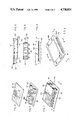
- FIG. 1 shows a prior art method for the assembly of current controlling devices
- FIG. 2 shows the process for mounting a printed circuit board assembly in a housing in accordance with the present invention
- FIG. 3 shows the assembly shown in FIG. 2 completed
- FIG. 4 shows a printed circuit board for supporting electronic components
- FIG. 5 shows the printed circuit board of FIG. 4 with the components attached and the leads formed
- FIG. 6 is an end view of the circuit board of FIG. 5 with the control circuit board attached;
- FIG. 7 is a perspective view of the assembly of FIG. 6;
- FIG. 8 is an end view of the housing partially cut away to show the circuit board assembly
- FIG. 9 is a view along the line 9--9 of FIG. 3.
- the overall purpose of the present invention is to package electronic components such as the power generators 20 and the required control circuitry in an efficient and effective manner.
- Electronic components such as power transistors generate considerable heat because of the high current densities transmitted thereby requiring packaging that spreads and dissipates the heat.
- the prior art shown in FIG. 1, illustrates art the power transistors 20 being mounted on a substrate 21 which then is cemented into the housing 24.
- the substrate 21 is made of a heat conducting material so as to carry heat from the power transistors and the integrated circuit 25 formed thereon. Such a substrate is commonly referred to as a heat spreader.
- the heat is conducted through the substrate to the base 27.
- the housing comprises side walls 26 fixed to a base 27 having mounting openings 28 in the ends.
- the opening 29 is closed by a cover (not shown) held in place by an adhesive.
- connection must be made between the external terminals 32 molded into the side wall 24 of the housing and the printed circuit 25.
- welded connections must be made between the ends 34 of the terminals 32 and soldered connections of connectors 35 fixed to and extending up from the printed circuit 25.
- solder connections are difficult to make and the soldering process creates the risk of damage to the printed circuit components on the substrate 21.
- the present invention was made to improve the process of encapsulating a power transistor circuit and the like such as that previously described.
- FIGS. 3 through 9 Illustrated in FIG. 3 is the desired assembly comprising a housing 40 similar in size to that shown in FIG. 1, and having connecting pins 41 extending through the wall 42 for making electrical contact. Access to the interior cavity of the housing is gained through the opening 43. As pointed out before, this housing is primarily to protect the circuits mounted therein.
- FIG. 4 a hybrid printed circuit board 45 having metal plates 46 to serve as printed circuits. These printed circuits are configured for making connections to the power transistors 47 illustrated in FIG. 5. While power transistors are shown, other electronic components can also be packaged in the manner to be described. The power transistors are soldered or cemented in the appropriate places to the printed circuit board for making suitable connections between the bases 48 of the components and the circuit conductors.
- the circuit board including the control circuitry shown in FIG. 1, must serve as a heat spreader and is thereby exposed to relatively high temperatures because of the heat generating effect created by the power components. It is the purpose of the present invention to isolate to the degree possible, the control circuitry from the primary heat generating components.
- the conductors 49 on the electronic components 47 are bent to extend upward away from the component circuit board 45 and are further configured to form a "C" shaped configuration 50 at the extended end as shown in FIGS. 5 and 6.
- the second or control printed circuit board 52 includes the control circuitry and other auxiliary circuits necessary for the power components 47.
- This control circuit board includes a printed circuit 54 and connectors 55 inserted between the extending conductors in the manner shown in FIG. 6.
- the printed circuit is configured to align with selected terminals 49 on the components and thus make electrical connection therewith.
- the connectors 55 connect with printed circuit portions on both sides of the second board to accommodate discreet components 56 on the underside of the board 52.
- the conductors 50 are soldered or otherwise attached to the second board 52 for mechanically supporting that board in spaced relationship with the first board 45 primarily to provide thermal isolation therefrom.
- FIG. 8 shows, the circuit board assembly 59 is mounted in the housing 40 with the terminals 55 extending through a slot 60 in the side wall 42.
- the slot 60 around the terminals 41 can be sealed with an insulating material to complete the housing enclosure.
- heat conducting cement can be placed between the first and second circuit boards and the wall members of the housing for better heat conduction.
- the housing also includes projections 62 which serve to better radiate heat into the surrounding atmosphere.
- components are assembled on a pair of printed circuit boards in a manner to thermally isolate the control components from the primary heat generating components and thereafter are placed into a housing with no additional solder connections necessary to complete the assembly.
Abstract
Description
Claims (8)
Priority Applications (1)
| Application Number | Priority Date | Filing Date | Title |
|---|---|---|---|
| US07/088,644 US4738024A (en) | 1987-08-24 | 1987-08-24 | Method of making a heat dissipating assembly |
Applications Claiming Priority (1)
| Application Number | Priority Date | Filing Date | Title |
|---|---|---|---|
| US07/088,644 US4738024A (en) | 1987-08-24 | 1987-08-24 | Method of making a heat dissipating assembly |
Publications (1)
| Publication Number | Publication Date |
|---|---|
| US4738024A true US4738024A (en) | 1988-04-19 |
Family
ID=22212565
Family Applications (1)
| Application Number | Title | Priority Date | Filing Date |
|---|---|---|---|
| US07/088,644 Expired - Fee Related US4738024A (en) | 1987-08-24 | 1987-08-24 | Method of making a heat dissipating assembly |
Country Status (1)
| Country | Link |
|---|---|
| US (1) | US4738024A (en) |
Cited By (12)
| Publication number | Priority date | Publication date | Assignee | Title |
|---|---|---|---|---|
| DE3942392A1 (en) * | 1988-12-23 | 1990-06-28 | Mazda Motor | VEHICLE CONTROL UNIT ASSEMBLY |
| DE3936906A1 (en) * | 1989-11-06 | 1991-05-08 | Telefunken Electronic Gmbh | Housing for electronic device in motor vehicle - has frame provided by inside surface fitted with two opposing carrier plates |
| US5310351A (en) * | 1992-10-29 | 1994-05-10 | Mcadow Theodore | Relay support circuit board unit |
| DE4305793A1 (en) * | 1993-02-25 | 1994-09-01 | Telefunken Microelectron | Power module |
| WO1999007197A1 (en) * | 1997-07-30 | 1999-02-11 | Energy Savings, Inc. | Heat spreader for electronic ballast |
| WO1999062168A1 (en) * | 1998-05-22 | 1999-12-02 | Intel Corporation | Packaging of a dc-to-dc converter |
| DE19959985A1 (en) * | 1999-12-13 | 2001-07-05 | Tyco Electronics Logistics Ag | Electronic circuit breaker, especially for on-board electrical network in motor vehicles, has thermally conductive carrier element, semiconductor elements, fixed conductors and control electronic circuit |
| US6269537B1 (en) * | 1999-07-28 | 2001-08-07 | Methode Electronics, Inc. | Method of assembling a peripheral device printed circuit board package |
| FR2888464A1 (en) * | 2005-07-07 | 2007-01-12 | Pierre Dumas | Thermal dissipation plate for e.g. printed circuit, has control circuit maintained inside frame and with potentiometer placed between aluminum foot fixation corners, and orifices placed in horizontal line in top and bottom parts |
| US20070053164A1 (en) * | 2005-09-06 | 2007-03-08 | Lear Corporation | Heat sink |
| DE102008060357A1 (en) * | 2008-12-03 | 2010-06-10 | Audi Ag | Electrical machine e.g. permanent magnet-excited synchronous machine, controlling device for use in motor vehicle, has cooling body arranged at side of power unit, and connecting arrangement arranged at other side of power unit |
| US20120071010A1 (en) * | 2010-09-22 | 2012-03-22 | Hitachi Automotive Systems, Ltd. | Electronic Control Device |
Citations (5)
| Publication number | Priority date | Publication date | Assignee | Title |
|---|---|---|---|---|
| US4204248A (en) * | 1978-11-20 | 1980-05-20 | General Electric Company | Heat transfer mounting arrangement for a solid state device connected to a circuit board |
| US4344106A (en) * | 1980-11-26 | 1982-08-10 | Rca Corporation | Transistor heat sink assembly |
| US4387413A (en) * | 1980-12-24 | 1983-06-07 | Rca Corporation | Semiconductor apparatus with integral heat sink tab |
| US4631819A (en) * | 1985-05-29 | 1986-12-30 | Motorola, Inc. | Low stress, tolerance free method for mounting power devices |
| US4669028A (en) * | 1986-02-18 | 1987-05-26 | Ncr Corporation | Heat sink for solid state devices connected to a circuit board |
-
1987
- 1987-08-24 US US07/088,644 patent/US4738024A/en not_active Expired - Fee Related
Patent Citations (5)
| Publication number | Priority date | Publication date | Assignee | Title |
|---|---|---|---|---|
| US4204248A (en) * | 1978-11-20 | 1980-05-20 | General Electric Company | Heat transfer mounting arrangement for a solid state device connected to a circuit board |
| US4344106A (en) * | 1980-11-26 | 1982-08-10 | Rca Corporation | Transistor heat sink assembly |
| US4387413A (en) * | 1980-12-24 | 1983-06-07 | Rca Corporation | Semiconductor apparatus with integral heat sink tab |
| US4631819A (en) * | 1985-05-29 | 1986-12-30 | Motorola, Inc. | Low stress, tolerance free method for mounting power devices |
| US4669028A (en) * | 1986-02-18 | 1987-05-26 | Ncr Corporation | Heat sink for solid state devices connected to a circuit board |
Cited By (17)
| Publication number | Priority date | Publication date | Assignee | Title |
|---|---|---|---|---|
| US5134546A (en) * | 1988-12-23 | 1992-07-28 | Mazda Motor Corporation | Vehicle control unit structure |
| DE3942392A1 (en) * | 1988-12-23 | 1990-06-28 | Mazda Motor | VEHICLE CONTROL UNIT ASSEMBLY |
| DE3936906A1 (en) * | 1989-11-06 | 1991-05-08 | Telefunken Electronic Gmbh | Housing for electronic device in motor vehicle - has frame provided by inside surface fitted with two opposing carrier plates |
| US5310351A (en) * | 1992-10-29 | 1994-05-10 | Mcadow Theodore | Relay support circuit board unit |
| DE4305793A1 (en) * | 1993-02-25 | 1994-09-01 | Telefunken Microelectron | Power module |
| US6091199A (en) * | 1997-07-30 | 2000-07-18 | Energy Savings, Inc. | Heat spreader for electronic ballast |
| WO1999007197A1 (en) * | 1997-07-30 | 1999-02-11 | Energy Savings, Inc. | Heat spreader for electronic ballast |
| US6212086B1 (en) * | 1998-05-22 | 2001-04-03 | Intel Corporation | Packaging of a DC-to-DC converter |
| WO1999062168A1 (en) * | 1998-05-22 | 1999-12-02 | Intel Corporation | Packaging of a dc-to-dc converter |
| US6269537B1 (en) * | 1999-07-28 | 2001-08-07 | Methode Electronics, Inc. | Method of assembling a peripheral device printed circuit board package |
| DE19959985A1 (en) * | 1999-12-13 | 2001-07-05 | Tyco Electronics Logistics Ag | Electronic circuit breaker, especially for on-board electrical network in motor vehicles, has thermally conductive carrier element, semiconductor elements, fixed conductors and control electronic circuit |
| FR2888464A1 (en) * | 2005-07-07 | 2007-01-12 | Pierre Dumas | Thermal dissipation plate for e.g. printed circuit, has control circuit maintained inside frame and with potentiometer placed between aluminum foot fixation corners, and orifices placed in horizontal line in top and bottom parts |
| US20070053164A1 (en) * | 2005-09-06 | 2007-03-08 | Lear Corporation | Heat sink |
| US7336491B2 (en) * | 2005-09-06 | 2008-02-26 | Lear Corporation | Heat sink |
| DE102008060357A1 (en) * | 2008-12-03 | 2010-06-10 | Audi Ag | Electrical machine e.g. permanent magnet-excited synchronous machine, controlling device for use in motor vehicle, has cooling body arranged at side of power unit, and connecting arrangement arranged at other side of power unit |
| US20120071010A1 (en) * | 2010-09-22 | 2012-03-22 | Hitachi Automotive Systems, Ltd. | Electronic Control Device |
| US8403682B2 (en) * | 2010-09-22 | 2013-03-26 | Hitachi Automotive Systems, Ltd. | Electronic control device |
Similar Documents
| Publication | Publication Date | Title |
|---|---|---|
| US5751058A (en) | Semiconductor device having parallel overlapping main current terminals | |
| EP0001892B1 (en) | Lead frame and package for establishing electrical connections to electronic components | |
| JP2791216B2 (en) | Package for electrical component, method for mounting power loss generating component, and method for connecting conductor terminal pin to circuit board | |
| JP3910497B2 (en) | Power circuit waterproofing method and power module having power circuit | |
| KR100474841B1 (en) | Wiring connection method and wiring connection structure | |
| US4738024A (en) | Method of making a heat dissipating assembly | |
| JPH07297575A (en) | Power module device | |
| JP6044473B2 (en) | Electronic device and method for manufacturing the same | |
| US20200076278A1 (en) | Electric machine | |
| JPH0661372A (en) | Hybrid ic | |
| US6905361B2 (en) | Electrical device | |
| JPH08148842A (en) | Electronic apparatus | |
| US5107074A (en) | Multi-lead hermetic power package with high packing density | |
| JP2736165B2 (en) | Hybrid circuit device | |
| JP2021158208A (en) | Electronic module | |
| JPH09246433A (en) | Radiation structure of module | |
| JP3156630B2 (en) | Power circuit mounting unit | |
| JPH0433657Y2 (en) | ||
| JP2512289B2 (en) | Resin-sealed semiconductor device | |
| JPS6240445Y2 (en) | ||
| JPH0697686A (en) | Hybrid integrated circuit device | |
| JPH11214875A (en) | Electronic component housing unit | |
| JP2851656B2 (en) | Manufacturing method of electronic equipment | |
| JPH09102684A (en) | Part mounting structure | |
| JPH0541563Y2 (en) |
Legal Events
| Date | Code | Title | Description |
|---|---|---|---|
| AS | Assignment |
Owner name: HYTEK MICROSYSTEMS INCORPORATED, 980 UNIVERSITY AV Free format text: ASSIGNMENT OF ASSIGNORS INTEREST.;ASSIGNOR:EBERHARDT, NOEL H.;REEL/FRAME:004773/0462 Effective date: 19870821 Owner name: HYTEK MICROSYSTEMS INCORPORATED,CALIFORNIA Free format text: ASSIGNMENT OF ASSIGNORS INTEREST;ASSIGNOR:EBERHARDT, NOEL H.;REEL/FRAME:004773/0462 Effective date: 19870821 |
|
| REMI | Maintenance fee reminder mailed | ||
| FPAY | Fee payment |
Year of fee payment: 4 |
|
| SULP | Surcharge for late payment | ||
| REMI | Maintenance fee reminder mailed | ||
| LAPS | Lapse for failure to pay maintenance fees | ||
| FP | Expired due to failure to pay maintenance fee |
Effective date: 19960424 |
|
| STCH | Information on status: patent discontinuation |
Free format text: PATENT EXPIRED DUE TO NONPAYMENT OF MAINTENANCE FEES UNDER 37 CFR 1.362 |