US4856899A - Optical frequency analyzer using a local oscillator heterodyne detection of incident light - Google Patents

Optical frequency analyzer using a local oscillator heterodyne detection of incident light Download PDF

Info

Publication number
US4856899A
US4856899A US06/943,670 US94367086A US4856899A US 4856899 A US4856899 A US 4856899A US 94367086 A US94367086 A US 94367086A US 4856899 A US4856899 A US 4856899A
Authority
US
United States
Prior art keywords
light
output
frequency
wavelength
analyzer
Prior art date
Legal status (The legal status is an assumption and is not a legal conclusion. Google has not performed a legal analysis and makes no representation as to the accuracy of the status listed.)
Expired - Lifetime
Application number
US06/943,670
Inventor
Hideto Iwaoka
Akira Ohte
Koji Akiyama
Current Assignee (The listed assignees may be inaccurate. Google has not performed a legal analysis and makes no representation or warranty as to the accuracy of the list.)
Yokogawa Electric Corp
Original Assignee
Yokogawa Electric Corp
Priority date (The priority date is an assumption and is not a legal conclusion. Google has not performed a legal analysis and makes no representation as to the accuracy of the date listed.)
Filing date
Publication date
Priority claimed from JP60287162A external-priority patent/JPS62145887A/en
Priority claimed from JP60294342A external-priority patent/JPS62154683A/en
Priority claimed from JP60296070A external-priority patent/JP2583410B2/en
Priority claimed from JP60296073A external-priority patent/JPS62156535A/en
Priority claimed from JP61011894A external-priority patent/JPS62171174A/en
Priority claimed from JP61040773A external-priority patent/JPS62198724A/en
Priority claimed from JP61040772A external-priority patent/JPS62198723A/en
Priority claimed from JP9617086U external-priority patent/JPS633172U/ja
Priority claimed from JP9819486U external-priority patent/JPS635661U/ja
Priority claimed from JP9761186U external-priority patent/JPH0331089Y2/ja
Priority claimed from JP61149777A external-priority patent/JPS637687A/en
Priority claimed from JP61168924A external-priority patent/JPS6324690A/en
Priority claimed from JP61189944A external-priority patent/JPS6345515A/en
Priority claimed from JP61199364A external-priority patent/JPS6355991A/en
Priority claimed from JP61221668A external-priority patent/JPS6377180A/en
Priority claimed from JP61260338A external-priority patent/JPS63115027A/en
Application filed by Yokogawa Electric Corp filed Critical Yokogawa Electric Corp
Assigned to YOKOGAWA ELECTRIC CORPORATION reassignment YOKOGAWA ELECTRIC CORPORATION ASSIGNMENT OF ASSIGNORS INTEREST. Assignors: AKIYAMA, KOJI, IWAOKA, HIDETO, OHTE, AKIRA
Application granted granted Critical
Publication of US4856899A publication Critical patent/US4856899A/en
Anticipated expiration legal-status Critical
Expired - Lifetime legal-status Critical Current

Links

Images

Classifications

    • HELECTRICITY
    • H01ELECTRIC ELEMENTS
    • H01SDEVICES USING THE PROCESS OF LIGHT AMPLIFICATION BY STIMULATED EMISSION OF RADIATION [LASER] TO AMPLIFY OR GENERATE LIGHT; DEVICES USING STIMULATED EMISSION OF ELECTROMAGNETIC RADIATION IN WAVE RANGES OTHER THAN OPTICAL
    • H01S5/00Semiconductor lasers
    • H01S5/06Arrangements for controlling the laser output parameters, e.g. by operating on the active medium
    • H01S5/068Stabilisation of laser output parameters
    • H01S5/0683Stabilisation of laser output parameters by monitoring the optical output parameters
    • H01S5/0687Stabilising the frequency of the laser
    • GPHYSICS
    • G01MEASURING; TESTING
    • G01JMEASUREMENT OF INTENSITY, VELOCITY, SPECTRAL CONTENT, POLARISATION, PHASE OR PULSE CHARACTERISTICS OF INFRARED, VISIBLE OR ULTRAVIOLET LIGHT; COLORIMETRY; RADIATION PYROMETRY
    • G01J9/00Measuring optical phase difference; Determining degree of coherence; Measuring optical wavelength
    • G01J9/04Measuring optical phase difference; Determining degree of coherence; Measuring optical wavelength by beating two waves of a same source but of different frequency and measuring the phase shift of the lower frequency obtained
    • GPHYSICS
    • G02OPTICS
    • G02FOPTICAL DEVICES OR ARRANGEMENTS FOR THE CONTROL OF LIGHT BY MODIFICATION OF THE OPTICAL PROPERTIES OF THE MEDIA OF THE ELEMENTS INVOLVED THEREIN; NON-LINEAR OPTICS; FREQUENCY-CHANGING OF LIGHT; OPTICAL LOGIC ELEMENTS; OPTICAL ANALOGUE/DIGITAL CONVERTERS
    • G02F2/00Demodulating light; Transferring the modulation of modulated light; Frequency-changing of light
    • G02F2/002Demodulating light; Transferring the modulation of modulated light; Frequency-changing of light using optical mixing
    • HELECTRICITY
    • H04ELECTRIC COMMUNICATION TECHNIQUE
    • H04BTRANSMISSION
    • H04B10/00Transmission systems employing electromagnetic waves other than radio-waves, e.g. infrared, visible or ultraviolet light, or employing corpuscular radiation, e.g. quantum communication
    • H04B10/50Transmitters
    • H04B10/501Structural aspects
    • H04B10/506Multiwavelength transmitters
    • HELECTRICITY
    • H04ELECTRIC COMMUNICATION TECHNIQUE
    • H04BTRANSMISSION
    • H04B10/00Transmission systems employing electromagnetic waves other than radio-waves, e.g. infrared, visible or ultraviolet light, or employing corpuscular radiation, e.g. quantum communication
    • H04B10/50Transmitters
    • H04B10/572Wavelength control
    • GPHYSICS
    • G01MEASURING; TESTING
    • G01JMEASUREMENT OF INTENSITY, VELOCITY, SPECTRAL CONTENT, POLARISATION, PHASE OR PULSE CHARACTERISTICS OF INFRARED, VISIBLE OR ULTRAVIOLET LIGHT; COLORIMETRY; RADIATION PYROMETRY
    • G01J3/00Spectrometry; Spectrophotometry; Monochromators; Measuring colours
    • G01J3/28Investigating the spectrum
    • HELECTRICITY
    • H01ELECTRIC ELEMENTS
    • H01SDEVICES USING THE PROCESS OF LIGHT AMPLIFICATION BY STIMULATED EMISSION OF RADIATION [LASER] TO AMPLIFY OR GENERATE LIGHT; DEVICES USING STIMULATED EMISSION OF ELECTROMAGNETIC RADIATION IN WAVE RANGES OTHER THAN OPTICAL
    • H01S3/00Lasers, i.e. devices using stimulated emission of electromagnetic radiation in the infrared, visible or ultraviolet wave range
    • H01S3/10Controlling the intensity, frequency, phase, polarisation or direction of the emitted radiation, e.g. switching, gating, modulating or demodulating
    • H01S3/13Stabilisation of laser output parameters, e.g. frequency or amplitude
    • H01S3/1303Stabilisation of laser output parameters, e.g. frequency or amplitude by using a passive reference, e.g. absorption cell

Definitions

  • This invention relates to an optical frequency analyzer having high accuracy and high resolving power.
  • a conventional optical frequency spectrum analyzer may be of the following types.
  • A One utilizing a diffraction grating or a prism as a spectroscope.
  • B One utilizing a Fabry-Perot resonator as a spectroscope.
  • two half mirrors HM are disposed to form a resonator.
  • This resonator has a resonant frequency (see FIG. 2) at a frequency interval of c/2L.
  • light to be measured is rendered incident upon the left half mirror HM, light having the frequency identical to the resonant frequency is transmitted through the half mirror HM and falls on receiving device PD.
  • half mirror HM is oscillated by means, for example, of a PZT or the like, in order to sweep the resonant frequency, the spectrum of the measurement light can be observed from the output from light receiving device PD.
  • wavelength resolving power becomes 0.1 nm (equivalent to about 30 GHz) or thereabout; and an absolute accuracy is about 2 nm (equivalent to about 600 GHz). These results are not favorable.
  • the optical frequency spectrum analyzer described in (B) shows results of the limit of frequency resolving power to about several tens of MHz. If the measurement if effected by inputting light having a reference wavelength, the absolute wavelength can be measured. The treatment is, however, very difficult, and accuracy is deteriorated (in connection with degreee of parallelism of mirrors and addjustment of perpendicular incidence, or error in frequency caused by fluctuations of an interval at which the mirrors are disposed). Furthermore, there is a defect in that it is impossible to simultaneously measure laser beams which are being oscillated in a plurality of modes.
  • FIG. 3 is a block diagram depicting a conventional optical fiber loss wavelength characteristic measuring device.
  • Output light from a variable wavelength light source VL enters a fiber MF to be measured, and the subsequent emergent light is detected by a photo detector PD.
  • the detected light is outputted as an electric signal to an amplifying/displaying circuit DP.
  • the characteristics of wavelength are measured from the variations of light power obtained when sweeping the output wavelength of the variable wavelength light source VL.
  • FIG. 4 is a block diagram showing a conventional optical fiber wavelength dispersion characteristic measuring device.
  • the variable wavelength light source VL and a reference wavelength light source SL are amplitude modulated by a modulation signal source Ef having a frequency f.
  • the photo detector member PD detects output optical powers both of measurement fiber Mf to which the output light of variable wavelength light source VL is applied and of reference fiber SF to which the output light of source SL is applied.
  • the phase differences in component of the frequency f between the two outputs are detected by a phase measuring device PS, thereby measuring a propagation delay time with respect to the wavelength of the measurement fiber MF.
  • the measuring devices depicted in FIGS. 3, 4 are deficient in many respects, such as, the optical phase propagation characteristics cannot be measured in a highly accurate manner.
  • the only acceptable measurement becomes possible with use of a long light path as in the case of optical fibers.
  • a short waveguide path is not acceptable for obtaining accurate measurements.
  • the measurement in regard to the propagation characteristic (e.g. loss, gain, phase, delay) and reflection characteristics is of importance to testing performance of such devices as the optical fiber, light waveguide path, wavelength branching filters, optical switches and the OEIC which are all essential components in any communication system or photo applied measurement systems.
  • the above described conventional devicees and systems are not sufficiently adequate.
  • an object of the invention is to overcome the aforementioned and other deficiencies and defects of the prior art.
  • Another object is to provide an optical frequency analyzer wherein light relative to incident light is made to fall upon an optical heterodyne detecting member together with frequency swept light outputted from an optical frequency sweeping member; and an electrical signal with a frequency corresponding to the difference between two frequencies is outputted and is then signal processed by a signal processing/displaying member through the intermediary of a filter, thereby making it possible to measure frequency characteristics of a measurement object with high accuracy, high resolving power and high stability.
  • FIGS. 1, 2 are diagrams depicting the principles of a conventional optical frequency spectrum analyzer.
  • FIG. 3 is a block diagram depicting a conventional optical fiber loss wavelength characteristic measuring device.
  • FIG. 4 is a block diagram depicting a conventional optical fiber wavelength dispersion characteristic measuring device.
  • FIG. 5 is a block diagram depicting a first illustrative embodiment of the invention.
  • FIGS. 6(a) and 6(b) is a time chart depicting operation of the embodiment of FIG. 5.
  • FIG. 7 is a graph depicting operation of the embodiment of FIG. 5.
  • FIG. 8 is a block diagram depicting a photo amplifying device.
  • FIG. 9 is a block diagram depicting a second illustrative embodiment of the invention.
  • FIG. 10 is a block diagram depicting details of a marker attached variable wavelength light source used in the embodiment of FIG. 9.
  • FIG. 11 is a spectrum chart depicting a marker signal output Em on the basis of frequency regions of the arrangement of FIG. 10.
  • FIG. 12 is a block diagram depicting a second example of the marker attached variable wavelength light source of FIG. 10.
  • FIG. 13 is a block diagram depicting a third example of the marker attached variable wavelength light source of FIG. 9.
  • FIG. 14 is a block diagram depicting a fourth example of a marker light source used in the arrangement of FIG. 9.
  • FIGS. 15(A), 15(B) and 15(C) are graphs depicting characteristic curves of the device of FIG. 14.
  • FIG. 16 is a block diagram depicting a fifth example of a marker light source used in the arrangement of FIG. 9.
  • FIG. 17 is a block diagram depicting a sixth example of a marker light source used in the arrangement of FIG. 19.
  • FIG. 18 is a graph depicting a characteristic curve of the device of FIG. 17 .
  • FIG. 19 is a block diagram depicting one example of a tunable laser user in the arrangement of FIG. 10.
  • FIG. 20 is a block diagram depicting a second example of a tunable laser.
  • FIG. 21 is a block diagram depicting a third example of a tunable laser.
  • FIG. 22 is a perspective view depicting a fourth example of a tunable laser.
  • FIG. 23 is a block diagram depicting one example of a reference wavelength laser light source used in the arrangement of FIG. 10.
  • FIG. 24 is a block diagram of a third illustrative embodiment of the invention.
  • FIG. 25 is a block diagram depicting a fourth illustrative embodiment of the invention.
  • FIG. 26 is a block diagram depicting one example of an optical frequency synthesizer/sweeper used in the embodiments of FIGS. 5 and 24.
  • FIG. 27 is a block diagram depicting a second example of the arrangement of FIG. 26.
  • FIGS. 28(A), 28(B) are wave charts showing characteristic curves of the arrangement of FIG. 27.
  • FIG. 29 is an energy diagram depicting energy levels of Rb gas.
  • FIG. 30 is a block diagram depicting a third, partially varied, example of the arrangement of FIG. 26.
  • FIG. 31 is a block diagram depicting a fourth example of the arrangement of FIG. 26.
  • FIG. 32 is a block diagram depicting another example of the optical frequency synthesizer/sweeper wherein a multiple light source is formed.
  • FIG. 33 is a graph depicting characteristic curves of the frequency spectrum of the output light of the arrangement of FIG. 32.
  • FIG. 34 is a block diagram depicting an example of a frequency stabilized semiconductor laser used as a reference wavelength light source.
  • FIG. 35 is an energy diagram showing a hyperfine structure of the energy level of a Cs atom.
  • FIG. 36 is a graph depicting optical absorption caused by the Cs atoms.
  • FIG. 37 is a diagram depicting operation of the arrangement of FIG. 34.
  • FIG. 38 is a graph depicting the characteristic curve of the arrangement of FIG. 34.
  • FIG. 39 is a block diagram depicting the principal portions of a second example of a frequency stabilized semiconductor laser.
  • FIG. 40 is a block diagram depicting the principal portions of an optical system of a third example of a frequency stabilized semi-conductor laser.
  • FIG. 41 is a block diagram depicting a fourth example of a frequency stabilized semiconductor laser.
  • FIG. 42 is a graph depicting an output signal from a lock-in amplifier used in the arrangement of FIG. 41.
  • FIG. 43 is a block diagram depicting principal portions of a fifth example of a frequency stabilized semiconductor laser.
  • FIG. 44 is a block diagram depicting principal portions of a sixth example of a frequency stabilized semiconductor laser.
  • FIG. 45 is a block diagram depicting principal portions of a seventh example of a frequency stabilized semiconductor laser.
  • FIG. 46 is a cross sectional view depicting principal portions of an eighth example of a frequency stabilized semiconductor laser.
  • FIG. 47 is a diagram depicting operation of the device of FIG. 46.
  • FIG. 48 is a block diagram depicting a ninth example of a frequency stabilized semiconductor laser.
  • FIG. 49 is a diagram depicting operation of the device of FIG. 48.
  • FIG. 50 is a block diagram depicting principal portions of a tenth example of a frequency stabilized semiconductor laser showing a partial modification of FIG. 48.
  • FIG. 51 is a block diagram of an eleventh example of a frequency stabilized semiconductor laser.
  • FIG. 52 is a diagram depicting operation of the device of FIG. 51.
  • FIG. 53 is a block diagram depicting principal portions of a twelfth example of a frequency stabilized semiconductor laser.
  • FIG. 54 is a block diagram depicting a thirteenth example of a frequency stabilized semiconductor laser.
  • FIG. 55 is a block diagram of a fourteen example of a frequency stabilized semiconductor laser, in principal portions thereof.
  • FIG. 56 is a block diagram depicting principal portions of a fifteenth example of a frequency stabilized semiconductor laser.
  • FIG. 57 is a block diagram depicting a sixteenth example of a frequency stabilized semiconductor laser.
  • FIGS. 58, 59 are graphs showing outputs of lock-in amplifiers used in FIG. 57.
  • FIG. 60 is a block diagram of a seventeenth example of a frequency stabilized semiconductor laser.
  • FIG. 61 is a block diagram depicting an eighteenth example of a frequency stabilized semiconductor laser.
  • FIG. 62 is a block diagram depicting principal portions of a nineteenth example of a frequency stabilized semiconductor laser.
  • FIG. 63, FIG. 64, and FIG. 65 are graphs showing Zeeman separation of the energy levels of Cs atom.
  • FIG. 66 is a perspective view depicting a twentieth example of a frequency stabilized semiconductor laser wherein the device is formed as an integrated circuit.
  • FIG. 67 is a table depicting a method of fabricating respective components of the device of FIG. 66.
  • FIGS. 68, 69 are perspective views depicting principal portions of another example of the device of FIG. 66.
  • FIGS. 70, 71, 72 are cross sectional views depicting principal portions of the device of FIG. 66.
  • FIG. 73 is a plan view depicting a twenty first example of a frequency stabilized semiconductor laser as laid out on an integrated circuit.
  • FIGS. 74(A), 75(B), 74(C) and 75 are perspective and plan views showing principal portions of another example of the arrangement of FIG. 73.
  • FIG. 76 is a block diagram depicting a twenty second example of a frequency stabilized semiconductor laser.
  • FIG. 77 is a diagram showing operation of the arrangement of FIG. 76.
  • FIG. 5 depicts an optical frequency analyzer which can perform frequency analysis.
  • the belt like arrow head indicates flow of photo or optical signals, while the solid line arrow head indicates flow of electrical signals.
  • the analyzer comprises a polarization control unit 1a which uses a magnetic optical effect crystal (YIG, lead glass or the like) in which measurement light, defining an object to be measured, is arranged to be incident light; a photo amplifying device 2a for for inputting output light from control unit 1a; a local oscillator 3a which constitutes an optical frequency sweeping device; a half mirror HM1a for inputting beams of output light from oscillator 3a and of amplifier 2a; an optical heterodyne detector 4a comprising e.g.
  • YIG magnetic optical effect crystal
  • PIN photodiode, avalanche photodiode, or the like for inputting output light from half mirror HM1a; filter 5a having a band pass property for inputting and amplifying electric output from heterodyne detector 4a; a detector for inputting electric output from filter 5a; and a signal processing/displaying circuit 72 for inputting electric output from detector 6a.
  • Local oscillator 3a comprises a sweeping signal generator 32a, reference wavelength light source 1s, and optical phase locked loop 2s for inputting light output from light source 1s. Loop 2s is arranged such that the frequency sweeping thereof is controlled by signal generator 32s and the output thereof is outputted to half mirror HM1a.
  • Photo amplifier 2a comprises a GaA1As laser (780 nm zone) and an ImGaAsP laser (1500 nm zone) and may utilize the following types of amplifiers.
  • a Fabry-Perot cavity type amplifier wherein bias electric current flows in the vicinity of the oscillation threshold value, signal light strikes a laser diode, and linear photo amplification is effected by inductive emission.
  • (C) A travelling wave type amplifier wherein both end surfaces of a laser diode chip are coated with non-reflective material, and photo amplification is performed by transmission of light.
  • Local oscillator 3a comprises an optical frequency synthesizer/sweeper, which will be described hereinbelow in greater detail, and which sweeps the wavelength of output from loop 2s by the output from generator 32a.
  • Loop 2s having output frequency ⁇ o , controls the wavelength of the output such as to correspond to an oscillation wavelength or reference source 1s, having output frequency ⁇ s.
  • a polarization plane of incident light is arranged to be identical to another polarization plane of the output from oscillator 3a by controlling the impressed magnetic field while utilizing rotary polarization of the magnetic optical effect crystal.
  • the output from control unit 1a is amplified by amplifier 2a and is then synthesized with the output from oscillator 3a by half mirror HM1a .
  • the electric output from heterodyne detector 4a is partially transmitted through filter 5a by its band pass properties and is taken out as power in detector 6a.
  • the processor/display unit 7a inputs electric output from detector 6a as a power signal and at the same time inputs a signal relative to the sweeping from generator 32a as a frequency axial signal, thereby spectrum displaying the measurement light.
  • wavelength of ⁇ s is 780 nm (wavelength of laser diode locked to absorption line of Rb); wavelength of ⁇ o is 1560 nm ⁇ 50 nm; and wavelength of ⁇ i is 1560 nm ⁇ 50 nm.
  • These operational frequency examples are confined to the case where the measurement light has the most suitable wavelength for optical communication. They are particularly effective in the measurement of characteristic (e.g. absolute wavelength, spectrum distribution and spectrum width) of light emitted from a laser diode in a communication system.
  • FIG. 5 a pulse synchronizing signal is added to generator 32a for the purpose of exhibiting such an example that the spectrum is, with pulse light serving as incident light, measured.
  • FIGS. 6(A), 6(B) time charts are provided to explain the operations of the above case.
  • a trigger signal (see FIG. 6(B)) synchronized with pulse light is inputted to generator 32a oscillator 3a. Synchronized with this, frequency ⁇ o of loop 2s is, as shown in FIG. 6(A), swept in a step configuration.
  • a signal, identical to that of FIG. 6(A), corresponding to the sweeping of frequency ⁇ o is transmitted to processor/display 72.
  • a power spectrum of ⁇ o exists at one point for every beam of pulse light and hence it is feasible to output the whole spectrum of pulse light depicted in FIG. 7 after sweeping operation has been completed.
  • the frequency resolving power of the optical frequency spectrum analyzer is determined both by the spectrum width of output frequency ⁇ o of oscillator 3a and the band width of filter 5a.
  • the spectrum width of frequency ⁇ o is likewise determined by the variable wavelength light source of the optical frequency synthesizer.
  • An external resonator type laser diode which will be discussed later with respect to FIGS. 19-22, is further used, whereby it is possible to obtain excellent frequency resolving power eg 100 KHz.
  • optical frequency spectrum analyzer which is highly precise, e.g. at 10 -12 , with absolute wavelength accuracy and which is highly stable.
  • the light pulse can be easily measured.
  • a W-Ni (tungsten, nickel) point contact diode and a Josephson element can be used for the heterodyne detector 4a.
  • a band pass filter is used as filter 5a, other filters can be used.
  • FIG. 8 depicts another example of a photo amplifier 2a.
  • the preferred arrangement is an optical frequency synthesizer/sweeper, such as shown in FIG.
  • the measurement frequency range will also be expanded except for the sweeping range of ⁇ o .
  • local oscillator OC1a which is capable of outputting a plurality of frequencies ⁇ L1 , ⁇ L2 . . . is used, it is feasible to obtain an even greater sweeping range.
  • FIG. 9 depicts another spectrum analyzer which differs from FIG. 5 as follows.
  • a marker attached variable wavelength light source 310a is arranged such that the frequency sweeping is controlled by sweeping signal generator 32a in local oscillator 30a that constitutes a sweeper.
  • Half mirror HM2a synthesizes reference wavelength light Rs and variable wavelength light Rv of the marker attached variable wavelength light source 310a.
  • Beams of output light from amplifier 2a and output from half mirror HM2a are synthesized in half mirror HM1a and are then supplied to heterodyne detector 4a.
  • Processor/display 7a inputs signal relative to the sweeping from generator 32a as the frequency axial signal and concurrently inputs electric output from detector 6a as the power signal. After this process, processor/display 7a spectrum displays a beam of measurement light 71a and a beam of reference light 72a and at the same time displays a marker 73a after inputting a marker electrical signal Em outputted from source 310a.
  • FIG. 10 depicts details of the source 310 of FIG. 9 which comprises an input terminal 11a to which a sweeping electrical signal Ei for controlling the wavelength is applied; a tunable laser 12a for inputting the sweeping electrical signal Ei through the intermediary of input terminal 11a; a beam splitter BS1a for bidirectionally splitting output from tunable laser 12a; a resonator FP1a which constitutes a marker light source, consisting of a Fabry-Perot etalon for inputting light transmitted through beam splitter BS1a; electro-optic element EO1a provided on the optical axis within resonator FP1a; a signal source E1a for driving element EO1a; a light receiving element PD1a for receiving output from resonator FP1a and for converting it to an electrical signal; and a highly accurate and stable reference wavelength laser light source 14a for emitting output light having a substantially constant wavelength.
  • a marker light source consisting of a Fabry-Perot
  • FIG. 10 embodiment Operation of the FIG. 10 embodiment is as follows.
  • Laser 12a emits output having a wavelength corresponding to signal Ei which is applied via input terminal 11a.
  • the output is reflected by beam splitter BS1a thereby to become the variable wavelength output Rv.
  • the rest is transmitted through beam splitter BS1a and are then inputted to resonator FP1a.
  • Resonator FP1a is capable of changing its equivalent resonator length by operation of electro-optic element EO1a, since element EO1a is present on the light path.
  • a beam of output light Rm from resonator FP1a produces a peak value at a wavelength interval corresponding to the output voltage from signal source E1a.
  • Light receiving element PD1 detects output RM and converts it into an electric signal which is outputted as a marker signal Em from terminal 13a.
  • FIG. 11 shows marker signal Em on the basis of frequency regions.
  • Reference source 14a emits output light Rs having a substantially constant wavelength within the scope of the output band of the variable light source 12a.
  • wavelength of reference light Rs is 780 nm (wavelength of laser diode locked to absorption beam of Rb); wavelength of variable wavelength light Rv is 780 nm ⁇ 50 nm; and wavelength of ⁇ i is 780 nm ⁇ 50 nm.
  • the frequency resolving power of the analyzer is determined by the spectrum width of the variable wavelength light Rv of source 310a and by the band width of filter 5a. Since the spectrum width of the variable wavelength light depends on tunable laser 12 of light source 310a, it is possible to obtain excellent frequency resolving power (e.g. of 100 KHz) by utilizing an external resonator type laser diode which will be explained with reference to FIGS. 19-22. Also, it is feasible to produce an analyzer which is highly accurate and stable at the absolute wavelength (e.g. in the range of 10 -12 ). Moreover, in the FIG. 10 embodiment, if the effective length of the Fabry-Perot etalon FP1a can be freely varied, the electro-optical element EO1a is not needed.
  • FIG. 12 depicts a variation of the marker attached variable wavelength light source 310a of FIG. 10 and comprises a beam splitter BS2a provided on the output light path for reference source 14a, for causing output light to be reflected and to strike beam splitter BS1a; a lock-in amplifier LA1a for inputting output from light receiving element, which is a detector , PD1a; a bias signal source E2a whose output is added to the output from lock-in amplifier LA1a and is then applied to electro optical element EO1a.
  • Some beams of output light from reference source 14a are reflected by beam splitter BS2a and fall via beam splitter S1a upon resonator FP1a.
  • the resonator length of resonator FP1a is controlled so that the reference wavelength component reaches its maximum in a feedback loop comprising lock-in amplifier LA1a, thereby making it possible to cause the marker light to accord with the reference wavelength.
  • FIG. 13 depicts details of the marker attached light source 310a for use in the arrangement of FIG. 9, and comprises an absorption cell CL1a which comprises a standard substance, e.g. Cs, for receiving light transmitted through beam splitter BS1a (this absorption cell CL1a constitutes a marker light source); a light receiving element or detector PD1a for receiving output Rm from absorption cell CL1a and converting it into an electrical signal; a comparator CP1a for receiving electric signals from detector PD1a; and a marker signal output terminal 13a connected to comparator CP1a.
  • an absorption cell CL1a which comprises a standard substance, e.g. Cs, for receiving light transmitted through beam splitter BS1a (this absorption cell CL1a constitutes a marker light source); a light receiving element or detector PD1a for receiving output Rm from absorption cell CL1a and converting it into an electrical signal; a comparator CP1a for receiving electric signals from detector PD1a; and a marker signal output
  • the standard source may comprise any of Cs (having two absorption beams in the vicinity of 852 nm), Rb (having four absorption beams in the vicinity of 780 nm, and four absorption beams in the vicinity of 794 nm), NH 3 (having a a plurality of absorption beams, and H 2 O (having a plurality of absorption beams.).
  • FIG. 13 arrangement Operation of the FIG. 13 arrangement is as follows. Part of the beams of output from tunable laser 12a is transmitted through beam splitter BS1a and strikes absorption cell CL1a. The incident light is subjected to absorption at a given wavelength by the standard substance and outputted as transmitted light Rm having peak value (i.e. the lowest point) at the stabilized wavelength. Element PD1a converts output light Rm into electrical signals which are waveform arranged. The arranged signal is, as marker signal Em, outputted from terminal 13a. Since quantum standard marker light is outputted, the wavelength can be measured with high accuracy.
  • FIG. 14 depicts another marker light source used in the source 310a of FIG. 9.
  • the arrangement comprises a light source LL1a having consecutive spectrums (this light source comprises an LED, a xenon lamp or the like); a lens LS1a for causing beams of output light from light source LL1a to be parallel; and a Fabry-Perot resonator FP2a comprising two seim-transparent mirrors, for acting on the output light from lens LS1a.
  • Source LL1a outputs light having a large width of spectrum as shown in FIG. 15(A).
  • the beams of light outputted from source LL1a are rendered parallel by lens LS1a and further enter resonator FP2a, thereby resonating between the two semi-transparent mirrors thereof.
  • Let the length of the resonator i.e. distance between the two semi-transparent mirrors
  • the transmissivity of the resonator as shown in FIG. 15(B), has a sharp peak for every c/2n 1 L 1 .
  • the light outputted from the semi-transparent mirror is as shown in FIG. 15(C). Accordingly, a reference marker can be produced with a simple device.
  • FIG. 16 depicts details of another marker light source for use in source 310a of FIG. 9, wherein the effective length of the resonator of FIG. 14 is varied.
  • the arrangement comprises an electro-optic crystal EO1a incorporated in the light path of the Fabry-Pero resonator FP2a; and a control signal source E1a connected to an electrode of the crystal EO1a.
  • control signal source E1a When an electric field is applied to crystal EO1a by control signal source E1a, the refractive index of crystal EO1a changes, whereby the equivalent or effective length of the resonator is varied.
  • the wavelength of the output light can be readily changed.
  • it is feasible to manufacture an optical frequency marker device wherein using a simple electrical device, the frequency can be varied by varying the effective resonator length.
  • the resonator may be placed in a constant temperature oven to control the temperature of the resonator to be substantially constant and produce a stable frequency interval.
  • FIG. 17 depicts details of a further marker source comprising a semiconductor laser LD1a comprising both ends which are AR-coated with non-reflective material; collimator lens LS2a, LS3a for causing the beams of output from laser LD1a to be parallel; semi-transparent mirrors HM3a, HM4a which form an external resonator disposed outside lens LS2a, LS3a; and an attenuator ATa through which light is outputted from semi-transparent mirror HM4a.
  • the output electric signal from detector PD2a is amplified by an amplifier A1a, and its waveform is monitored by a spectrum analyzer SAa.
  • FIG. 17 Operation of the FIG. 17 embodiment is as follows with reference to FIG. 18.
  • a gain curve of spontaneous emitted output light from laser LD1a is depicted as indicated by a dotted line (a) in FIG. 18.
  • the free spectrum range of the external resonator is determined by c/2n 2 L 2 , and as indicated by a dotted line (b) in FIG.
  • the marker output light outputted from attenuator ATa is characterised (i.e. multiple modes oscillation) as shown by the solid line (c) in FIG. 18.
  • FIG. 19 depicts details of a tunable laser 12a used in the marker attached variable wavelength light source 30a of FIG. 10, wherein an element having wavelength selectivity is incorporated in the resonator.
  • the arrangement comprises a semiconductor laser LD2a; non-reflection coated surfaces 121a, 122a provided at both ends of the laser LD2a; lens LS5a for causing beams of light emerging from non-reflection surface 121a to be parallel; half mirror HM5a on which light transmitted through lens LS5a is reflected (this half mirror outputs resonant light to the outside); lens LS6a for causing light emerging from non-reflection surface 122a to be parallel; a first acousto-optical modulator UM1a for receiving light which is transmitted through lens LS6a; a second acousto-optical modulator UM2a for receiving light outputted from modulator UM1s; a mirror M1a for reflecting light emerging from modulator UM2a; and an oscil
  • the beams of light which emerge from non-reflection surface 121a of laser LD2a are arranged to be parallel in lens LS5a and are then reflected by half mirror HM5a. The reflected beams of light travel back through the light path and strike laser LD2a once again.
  • the beam of light having a frequency fo 1 which emerges from non-reflection surface 122a are arranged to be parallel by lens LS6a and strike modulator UM1a.
  • the wavelength of such light varies so as to satisfy given incident and emergent angles with respect to a diffraction grating created by ultrasonic waves, if the wavelength of the ultrasonic wave applied to modulators UM1a, UM2a changes.
  • the incident light is subjected to Doppler shift caused by the ultrasonic waves, and the frequency of +1-dimensional diffracted light (the direction of ultrasonic waves is the same as the diffracted direction) becomes fo 1 +F.
  • the emergent light from modulator UM1a is diffracted in modulator UM2a once again.
  • modulator UM2a the relation between diffraction light--and direction in which ultrasonic waves travel is opposite to that in modulator UM1a; and 1-dimensional diffraction light is therefore present.
  • the volume of Doppler shift amounts to -F
  • the output light from modulator UM1a undergoes Doppler shift in modulator UM2a after being reflected by mirror M1a.
  • the wavelength (frequency F) of the ultrasonic wave is varied, it is feasible to sweep the wavelength of the resonant light.
  • the light which has been resonated is outputted via half mirror HM5a to the outside.
  • FIG. 20 describes a tunable laser having incorporated in the resonator an element capable of controlling the refractive index of light.
  • the arrangement comprises an electro-optic device EO1a, both surfaces of which are coated with non-reflection material and comprises LiNbO 3 (niobium acid lithium) or the like and receives output from lens LS6a; and a signal source E2a for controlling element EO1a.
  • the beams of light which have merged from laser LD2a are arranged to be parallel by lens LS6a and one is transmitted to electro-optic device HO1a. The transmitted light travels back through the previous light path after being reflected by mirror M1a and strikes laser LD2a once again.
  • a resonator can be constructed between half mirror HM5a and mirror M1a.
  • the distance, exclusive of a length along the light path for the electro-optic device EO1a, between half mirror HM5a and mirror M1a be L 3
  • light velocity be c
  • integer be p
  • refractive index be n 3 .
  • oscillation frequency fo 2 is
  • the refractive index n 3 can be varied by changing the intensity of electric field applied to electro-optic device EO1a, using electric signals from source E2a, thereby making it possible to sweep ("sweep" can be construed in some instances to mean control) oscillation frequency fo 2 .
  • FIG. 21 depicts details of another tunable laser 12a wherein double resonators are shown.
  • the arrangement comprises a beam splitter BS3a for bidirectionally splitting the emergent light from lens LS6a; electro-optic device EO2a upon which light transmitted through beam splitter BS3a falls; mirror M1a on which the emergent light from electro-optic device EO2a is reflected; electro-optic device EO3a for receiving light reflected by beam splitter BS3a; and mirror M2a for reflecting emergent light from device EO3a.
  • the lengths, extending along the light path, of the electro-optic devices EO2a, EO3a be l 4 , l 5 , respectively; let the refractive index be n 4 , n 5 , respectively; let distinace exclusive of length l 4 extending along the light path between half mirror HM5a and mirror M1a be L 4 ; let the distance, exclusive of length l 5 , extending along the light path between the half mirror HM5a and mirror M2a be L 5 ; and let the integer be q. Then, in this case, the oscillation frequency fo 3 is
  • FIG. 22 depicts the tunable laser of FIG. 20 arranged on a single semiconductor chip in an integrated circuit, and comprises a laser diode 123a formed of AlGaAs, InGaAsP; a photo amplifier 124a provided at the joined portion of laser diode 123a; a waveguide path type external resonator 125a; mirrors 126a, 127a provided at both ends of laser diode 123a; an electrode 128a provided on the surface of laser diodes 123a such as to correspond to photo amplifier 124a; and electrode 129a provided on the surface such as to correspond to the waveguide path type external resonator 125a.
  • An electric current I LD is supplied to the joint through electrode 128a, and laser beams are emitted to photo amplifier 124a.
  • An electric current I F is supplied via electrode 129a to resonator 125a and the refractive index of resonator 125a is varied, thereby sweeping the oscillation frequency.
  • FIG. 23 depicts details of a reference wavelength laser light source 14a, such as used in the marker attached source 310a of FIG. 10 and comprises a semiconductor laser LD3a; a beam splitter BS4a upon which output light from laser LD3a strikes; an absorption cell CL2a comprising a standard substance, e.g.
  • the light transmitted by beam splitter BS4a becomes the output light of the source.
  • the standard substance may also be Rb, NH 3 or H 2 O.
  • the output light from laser LD3a is reflected by beam splitter BS4a, strikes absorption cell CL2a and is subjected to absorption by the standard substance therein.
  • the quantity of absorption is detected by detector PD3a and is fed back via lock in amplifier LA1a to the electric current applied to laser LD3a.
  • the output wavelength of laser LD3a is locked to absorption spectral beams of the standard substance, so that a reference wavelength light is produced by the source with high accuracy and high stability.
  • One method of absorption is using the linear absorption method.
  • the absorption spectrum becomes relatively large in thickness by virtue of the Doppler shift.
  • the absorption beams having a hyperfine structure which are hidden due to the Doppler shift are detected by saturated absorption spectroscopy (see T. Yabuzaki, A. Hori, M. Kitano, and T. Ogawa, "Frequency Stabilization of Diode Lasers Using Doppler Free Atomic Spectra", Proc. Int. Conf. Laser, 1983).
  • the oscillation wavelength of the laser LD3a is locked to the thus detected absorption beams, whereby much higher stability can be obtained.
  • FIG. 24 depicts one such synthesizer/sweeper is depicted.
  • the synthesizer/sweeper 31a sends forth a frequency swept light output (constituting an optical frequency sweeping device), and will be discussed with respect to FIG. 26.
  • a sweeping signal generator is omitted from this FIG. 24 arrangement.
  • the arrangement of FIG. 24 The arrangement of FIG.
  • optical frequency analyzer comprises the frequency synthesizer/sweeper 31a; an optical heterodyne detecting member 223a for inputting first and second beams of output light from synthesizer/sweeper 31a; filter 224a comprising a band pass filter for inputting electric output from optical heterodyne detector 223a; optical directivity coupler 220a which inputs a first beam of output light from optical frequency synthesizer/sweeper 31a; an emergent terminal 23a from which output light from optical directivity coupler 220a emerges; an object to be measured 210a for receiving output light from emergent terminal 230a; an incident terminal 240a upon which light emerging from object 210a strikes; a polarization control unit 241a which makes use of a magnetic optical effect crystal (YIG, lead, glass or the like) for inputting incident light from incident terminal 240a; a photo amplifier 242a for inputting output from polarization control unit 241a; an optical heterodyne detector
  • a first optical heterodyne detector may be considered to comprise heterodyne detectors 233a, and 243a.
  • a first filter device may be considered to comprise filters 234a and 244a.
  • a second optical heterodyne detector may be considered to comprise detector 223a.
  • a second filter device may be considered to comprise filter 224a.
  • a comparison means may be considered to comprise phase comparators 236a, and 246a and amplitude comparators 235a and 245a.
  • a signal processing means may be considered to comprise signal processing/displaying device 250a.
  • the photo amplifiers may be similar to the photoamplifier 2a shown in FIG. 5.
  • Heterodyne detectors 233a, 223a and 243a may be similar to the optical heterodyne detector 4a shown in FIG. 5.
  • Synthesizer/sweeper 31a frequency sweeps the light output, and outputs it with high accuracy and high stability and high spectral purity.
  • the first light output which is outputted from synthesizer/sweepr 31a is frequency shifted by ⁇ by an optical frequency shifter (not shown) comprising an ultrasonic modulator, thereby becoming a second light output.
  • the first light output, having a frequency ⁇ o from synthesizer/sweeper 31a strikes object 210a via coupler 220 and terminal 230a, and the emergent light from the object 210a is inputted via incident terminal 240a to control unit 241a.
  • Control unit 241a controls an impressed magnetic field by making most of the rotary polarization of its magnetic optical effect cyrstal, and a polarization plane of the input light is thereby arranged to be identical with that of the local oscillation light (second light output).
  • the output from control unit 241a is synthesized with the local oscillation light from synthesizer/sweeper 31a by a half mirror (not shown) after being amplified by photo amplifier 242a.
  • the electric output from heterodyne detector 243a is partially transmitted through filter 244a due to its band pass filter properties and becomes a reference signal.
  • the first output, having frequency ⁇ o from synthesizer/sweeper 31a is directly synthesized with local oscillation light having frequency ⁇ o + ⁇ , by a half mirror or the like, and is then converted into an electrical signal having a frequency equivalent to the difference ⁇ between the two frequencies by heterodyne detector 223a and outputted to filter 224a.
  • the electrical signal output which is influenced by the properties of object 210a, from filter 244a and a reference signal, which is not influenced by the properties of object 210a, from filter 224a are compared with respect to the amplitudes thereof in amplitude comparator 245a and are further compared with respect to the phase thereof in phase comparator 246a.
  • the electric outputs from amplitude comparator 245a and phase comparator 246a are signal processed by signal processing/displaying device 250a, whereby the propagation characteristics of object 210a are displayed.
  • the reflected light outputted from object 210a via emergent terminal 230a and directivity coupler 220a is likewise consecutively processed in polarization control unit 231a, photo amplifier 232a, heterodyne detector 233a, filter 234a, amplitude comparator 235a, phase comparator 236a, and signal processing/displaying circuit 250a, whereby the reflection characteristics of object 210a are displayed.
  • the light waveguide path is an object to be measured
  • an optical fiber is the object to be measured
  • a laser diode photo amplifier is the object being measured
  • the wavelength characteristics of amplification gain, phase delay, and the like can be measured.
  • reflection loss at an optical contact point can be measured from the characteristics of the reflected light.
  • filters 224a, 234a, 244a comprise band pass filters.
  • Wavelength ⁇ s is 780 nm (wavelength of laser diode locked to absorption beam of Rb); Wavelength of ⁇ o is 1560 nm ⁇ 50 nm; and Frequency of ⁇ is 100 MHz. These frequencies are the most suitable for optical communication systems, and also effective in the measurement of light communication devices.
  • the reference signal used for the comparison device is obtained using second heterodyne detector 223a and second filter 224a.
  • the invention is not limited to these types of devices.
  • a modulation signal (corresponding to shift frequency ⁇ ) applied to a frequency synthesizer/sweeper 31a may be used.
  • the configuration can be simplified by omitting heterodyne detector 223a and filter 224a.
  • the light which emerges from the network analyzer and travels to the object 210a is not limited to continuous light but may comprise pulse light. It is also feasible to measure the wavelength characteristics with respect to a pulse light by sweeping the optical frequency while synchronizing with the pulse light.
  • FIG. 25 describes a further analyzer similar to FIG. 24 except that a frequency sweeping device comprising marker attached variable wavelength light source 310a, similar to that used for the spectrum analyzer of FIG. 9, is used instead of synthesizer/sweeper 31a.
  • a sweeping signal generator also is omitted.
  • a first variable wavelength output supplied from source 310a is frequency shifted by ⁇ by an optical frequency shifter (not shown) thereby forming a second light output.
  • Marker signal output Em from source 310a is inputted directly to signal processing/displaying device 250a, whereby a marker is displayed together with the respective characteristics.
  • Wavelength ⁇ o is 1560 nm ⁇ 50 nm; and Frequency of ⁇ is 100 MHz. These frequencies are suitable for optical communication and measurement.
  • the FIG. 25 embodiment is simple and can precisely measure various frequency characteristics, such as phase, amplitude, and the like, using a simple variable frequency light source and by correcting the wavelength with use of a marker.
  • the second light output from variable source 22s may be used as an input light for the optical frequency marker.
  • FIG. 26 An example of the synthesizer/sweeper used in FIGS. 5, 24, is depicted in FIG. 26, and comprises reference wavelength light source 1s in which wavelength is stabilized; optical phase locked loop 2s for receiving light output from source 1s; photo modulator 3s for modulating output from loop 2s; and photo amplifier 4s for amplifying output from modulator 3s.
  • Phase locked loop 2s comprises an optical heterodyne detector 21s which receives light, as an input at one side, from source 1s; variable wavelength light source 22s wherein the oscillation wavelength of output light is controlled by an electric output from heterodyne detector 21s; frequency shifter 23a for shifting the frequency of output from light source 22s; and optical frequency multiplier 24s for multiplying the frequency of output from shifter 23s and for supplying the output thereof as an input to the other side of heterodyne detector 21s.
  • loop 2s fixes, i.e. locks, the wavelength of the output to one corresponding to the oscillation wavelength of reference source 1s.
  • heterodyne detector 21s makes a comparison between the output light emitted from source 1s and output from multiplier 24s, and controls source 22s so as to diminish the difference between the two.
  • Shifter 23s in a feedback circuit, adds an offset frequency to the output light from source 22s.
  • Multiplier 24s determines the ratio of frequency of output from source 1s to the frequency of output from source 22s.
  • Modulator 3s modulates the output from loop 2s using another signal applied thereto.
  • Amplifier 4s amplifies the output from modulator 3s and supplies the output as an output from the synthesizer/sweeper.
  • FIG. 27 depicts greater details of the components of FIG. 26 wherein light source 1s comprises a laser diode LD1s; absorption cell CL1s for receiving output light from laser diode LD1s and comprising Rb gas or Cs gas as the standard substance half mirror HM1s upon which output light from cell CL1s falls, photo diode PD1s for inputting light reflected by half mirror HM1s; control circuit A1s for inputting electric output from photo diode PD1s and for controlling electric current applied to laser diode LD1s by an output corresponding to the electric signal from PD1s; a returning light preventing isolator IS1s through which light transmitted through half mirror HM1s passes; and photo amplifier OA1s to which light penetrating isolator IS1s is inputted.
  • light source 1s comprises a laser diode LD1s; absorption cell CL1s for receiving output light from laser diode LD1s and comprising Rb gas or Cs gas as the standard
  • Phase locked loop 2s comprises half mirror HM2s to which is applied output from source 1s; photodiode PD2s comprising a PIN photodiode, avalanche photodiode, or the like, for inputting light transmitted through half mirror HM2s (photodiode PD2s constitutes heterodyne detector 21s); an oscillator ECs which generates an electric signal having a predetermined frequency by inputting reference frequency from a crystal; an a mixer circuit MX1s to which both the electric output from oscillator ECs and electric output from heterodyne detector PD2s are connected and having an output supplied to source 22s.
  • the variable wavelength light source 22s comprises frequency modulating circult FCs to which is applied output from mixer MX1s; tunable laser diodes VL1s, VL2s, VL3s for receiving outputs from frequency modulating circuit FCs; isolators IS2s through which fluxes of output light from diodes VL1s, VL2s, VL3s pass (isolators IS2s comprise YIG, for example); and an optical switch OS1s for receiving respective outputs from isolators IS2s.
  • the loop 2s further comprises half mirror HM3s upon which the output from switch OS1s strikes; photo amplifier OA2s for receiving output light reflected by half mirror HM3s; an ultrasonic modulator UM1s for receiving output light from photo amplifier OA2s (modulator UM1s constitutes the optical frequency shifter 23s); light waveguide path NLs comprising a non-linear material, for receiving output from shifter 23s (path NLs constitutes the frequency multiplier 24s); and photo amplifier OA3s for amplifying the output from path NLs.
  • Photo modulator 3s which receives output from loop 2s, comprises amplitude modulator AM1s and phase modulator PM1s, both comprising electro-optical crystals, such asLiNbO 3 ; polarizing modulator LM1s which uses a magneto-optical crystal such as YIG.
  • Photo amplifying member 4s comprises photo amplifier OA4s and amplifies the output from photo modulator 3s.
  • Source 1s controls the oscillation wavelength of laser diode LD1s to absorption beams of Rb or Cs atoms, for example, thereby producing high accuracy and high stability (e.g. at more than 10 -12 ) at an absolute wavelength. If the wavelength of the output from laser diode LD1s, when passing through absorption cell CL1s, accords with the absorption beams of Rb gas (or Cs gas), the output from diode LD1s is absorbed.
  • the absorptive properties are shown in FIG. 28(A).
  • FIG. 29 depicts an energy level diagram of Rb gas.
  • the absorption beams of Rb are such that a D 2 beams is 780 nm and a D 1 beam is 795 nm. If the beams are multiplied, the results become 1560 nm and 1590 nm, respectively. These numeric values fall within a zone of 1500 nm which is preferred for optical communications, and for photo applied measurements.
  • Some fluxes of output from cell CL1s are reflected by half mirror HM1s and are then detected by photo detector PD1s. Thereafter, the output wavelength from laser diode LD1s is locked to the center of absorption by controlling the electric current applied to laser diode LD1s in control circuit A1s such as to correspond to the output from photodetector PD1s.
  • the output wavelength is to be locked to a point a s of FIG. 28(A)
  • it is fixed to a point b s (value of differential waveform becomes zero) of FIG. 28(B) which is a differential waveform of FIG. 28(A) in control circuit A1s by using a lock-in amplifier. This is referred to as the "linear absorption method".
  • the absorption spectrum becomes wide as in the case of FIG. 28(A).
  • absorption beams of a hyperfine structure which are concealed on account of Doppler shift, are detected by "saturated absorption” spectroscopy, and if the oscillation wavelength of laser diode LD1s is locked to the detected absorption beams, still higher stability is obtained.
  • Laser diode LD1s can be stabilized in temperature by use of a constant temperature oven.
  • the light transmitted by half mirror HM1s strikes isolator IS1s.
  • Isolator IS1s prevents light returned from the outside by reflection from changing into noises.
  • the output from isolator IS1s is, as occasion arises, amplified by photo amplifier OA1s.
  • Loop 2s locks the oscillation wavelength of variable source 22s to the oscillation wavelength of reference source 1s at a predetermined offset and ratio.
  • the output from source 1s passes through half-mirror HM2s and falls upon photo diode PD2s of heterodyne detector 21s.
  • Light fed back from multiplier 24s is amplified by photo amplifier OA3s and reflected by half mirror HM2s and then strikes photo diode PD2s.
  • a resonator is constituted by making the most of the reflection on a diffraction grating incorporated in a diode chip and the oscillation frequency is determined by the pitch of the diffraction grating
  • a DFB distributed feedback
  • ADFB acoustic DFB
  • DBR distributed Bragg Reflector
  • the ADFB laser generates a surface elastic wave (SAW) such as to be orthogonal to the diffraction grating provided within the DBR laser, and forms an optical ring resonator based on Bragg diffraction which requires the diffraction grating which is incorporated in the chip and the surface eleastic wave.
  • SAW surface elastic wave
  • the resonant wavelength of the ring resonator varies, thereby making it possible to sweep the oscillation wavelength.
  • the oscillation wavelength falls within a zone of 1560 nm.
  • the DFB laser, the DBR laser and the ADFB laser which individually include a lengthy resonator have advantages in that the oscillation spectrum is narrow, and the spectrum has good purity.
  • a plurality of ADFB lasers VL1s, VL2s, VL3s
  • FIG. 27 whereby it is feasible to perform change-over operation with the aid of an optical switch or light wave synthesizer.
  • the fluxes of output light from diodes VL1s, VL2s, VL3s are inputted via isolators IS2s to optical switch OS1s, wherein light having a desired variable wavelength range is selected.
  • the fluxes of output light from switch OS1s is partially reflected by half mirror HM3s and are then inputted to photo amplifier OA2s.
  • the output from amplifier OA2s is inputted to shifter 23s and applied to modulator UM1s, thereby outputting Bragg's s-dimensional diffracted light.
  • a reference frequency source such as a crystal oscillator
  • the optical frequency of the diffracted light shifts be s 107 5.
  • the output from shifter 23s strikes multiplier 24s, and a secondary higher harmonic wave of the input light is outputted at waveguide path NLs.
  • the tunable laser diode output of 1560 nm is inputted through photo amplifier OA2s, and a signal of 780 nm of a secondary higher harmonic wave is outputted.
  • a waveguide path NLs there is used a slab light waveguide path having a quadruple layer of air-TiO 2 -ZnS-glass wherein a non-linear thin film of ZnS and a linear thin film of TiO 2 are used in order that non-linear effects are produced with high efficiency.
  • the secondary higher harmonic wave is utilized; however, discretionary n-dimensional higher harmonic wave may also be used.
  • the output from multiplier 24s is amplified by photo amplifier OA3s. Thereafter, at half mirror HM2s the output light from multiplier 24s is, as the feedback light, brought into confluence with output from source 1s.
  • the optical frequency ⁇ o of output loop 2s is
  • the optical frequency multiple n is 2. That is, ⁇ o is, at the predetermined ratio of n, locked to optical frequency ⁇ s which assumes high accuracy and high stability at the absolute wavelength, and has an offset of an arbitrary frequency ⁇ 3 /n or just ⁇ 5 . If ⁇ 3 or ⁇ 5 is swept, it is possible to realize highly accurate sweeping of optical frequency. Since ⁇ 3 and ⁇ 5 are electrical signals, high accuracy and high stability can be readily obtained.
  • the output from loop 2s is inputted to modulator 3s and is amplitude modulated by means of an amplitude modulator AM1s. It is further modulated in phase by a phase modulator PM1s, and is then varied with respect to the direction of polarization by a polarization modulator LM1s. After light output from modulator 3s is amplified by amplifier OA4s of photo amplifier 4s, the amplified output becomes the output of the synthesizer.
  • amplifier OA1s to OA4s are the same as those utilized in amplifier 2a of FIG. 5. Also, the positions of shifter 23s and multiplier 24s may be interchanged. The frequency ⁇ o of output from loop 2s may be
  • both mixers MX1s and shifter 23s are designed for adding offset frequencies, and any one of them may be omitted.
  • loop 2a may have its multiple n be 1, in which case, the multiplier 24s may be omitted.
  • the absorption beams of Rb of Cs are used in absorption cell CL1s of source 1s, other standard substances may be used, such as NH 3 or H 2 O. Since the discretionary beams (1500 nm zone) of NH 3 are highly accurate and stable at the absolute wavelength, multipler 24s may be omitted in that case. Also, it is feasible to stabilize the wavelength by using a Fabry-Perot resonator as a wavelength detector. However, utilizing absorption beams that are standard in terms of quantum is superior to using such Fabry-Perot resonator.
  • the tunable laser diodes VL1s,VL2s,VL3s are not limited to the ADFB laser used in the embodiment.
  • an external resonator may be used which adopts the diffraction grating added to the outside of the laser diode chip with the diffraction grating being made to rotate, and a variable wavelength is obtained by making the most of its wavelength selectivity.
  • a narrow spectrum is characteristic of such external resonator type laser diode.
  • the devices of FIGS. 19-22 may be used.
  • FIG. 30 depicts details of heterodyne detector 21s (of FIG. 27) which comprises local oscillator OLs of a optical frequency ⁇ L which utilizes a second wavelength stabilizing source; an optical frequency mixer OXs to which output from oscillator OCs and multiplier 24s are inputted via photo amplifier OA3s (this mixer comprises non-linear optical crystal); and a photo detector ODs comprises a PIN diode, an avalanche photo diode, or the like, for receiving output from mixer OXs and output from reference source 1s and for outputting electrical siganls to variable source 22s.
  • FIG. 31 describes an embodiment similar to FIG. 26, but of a synthesizer/sweeper which is capable of simultaneously outputting two optical frequencies.
  • the arrangement comprises a reference wavelength light source 1s and phase locked loop 2s.
  • the source 1s is a two wavelength stabilized laser diode which utilizes saturated absorption method and comprises laser diodes LD11s, LD12s, which generate laser outputs having different wavelengths; half mirror HM4s for causing the outputs from lasers LD11s, LD12s to become confluent with each other; half mirror HM5s for bidirectionally splitting output from half mirror HM4s; absorption cell CL1s (similar to that of FIG.
  • Optical phase locked loop 2s is similar to FIG. 27, but differs in the following respects.
  • Mixers MX11s, MX12s are provided for inputting an electric output from heterodyne detector 21s and FM modulation frequencies ⁇ A , ⁇ B .
  • the variable source 22a comprises frequency modulation circuits FC1s, FC2s (which have LPF properties) for receiving outputs from mixers MX11s, MX12s; tunable laser diodes VL4s,VL5s, the oscillation frequencies thereof being controlled by the outputs from circuits FC1s, FC2s; returning light preventing isolators IS21s, IS22s for receiving outputs from respective tunable laser diodes VL4s, VL5s and preventing reflected light from becoming noise; and light wave synthesizer OS2s for inputting and synthesizing light outputs from isolators IS21s, IS22s.
  • the other components are the same as that of FIG. 27.
  • the operation of the FIG. 31 embodiment is as follows. Provided that the outputs from diodes LD11s, LD12s are ⁇ A + ⁇ A , ⁇ B + ⁇ B , the two fluxes of light are synthesized in half mirror HM4s and are bidirectionally split by half mirror HM5s. The light transmitted through half mirror HM5s is supplied as saturation light to cell CL1s. Thereafter, the light is transmitted through half mirror HM6s and is then outputted via isolator IS1s to loop 2s.
  • half mirror HM5s light reflected by half mirror HM5s is further reflected by mirror M4s and is then split bidirectionally by half mirror HM7s.
  • Light passing through half mirror HM7s is diaphragmed by diaphragm LS3s and is reflected by half mirror HM6s.
  • the reflected light becomes probe light which is much narrower than the saturation light and is supplied to absorption cell CL1s.
  • the light is subjected to absorption accompanied with a sharp cavity formed in Doppler expansion by the saturation effect, is reflected by half mirror HM5s and strikes photo detector PD11s.
  • Light that is reflected by half mirror HM7s, serving as reference light is applied from a perpendicular direction to cell CL1s and then undergo absorption coupled with Doppler expansion.
  • Differential amplifier A2s computes the difference between electric outputs from photo detectors PD11s, PD12s and then supplies a difference signal to lock-in amplifiers LA1s, LA2s.
  • ⁇ A ⁇ 1A , and ⁇ B ⁇ 1B During operation of loop 2s, ⁇ A ⁇ 1A , and ⁇ B ⁇ 1B . Since ⁇ A , ⁇ B are several KHz and the difference between ⁇ A and ⁇ B is, as shown in FIG. 29, 6.8 GHz, it is feasible to take out only the frequency components of
  • ; ⁇ 4B
  • the frequency modulation circuits FC1s and FC2s respectively control oscillation frequencies of variable wavelength diodes VL4s, VL5s so that the frequencies of the output signals ⁇ 4A and ⁇ 4B from mixers MX11s, MX12s come to zero.
  • the light outputs from laser didoes VL4s, VL5s are supplied via isolators IS21s, IS22s, to synthesizer OS2s wherein the outputs are synthesized, thereby generating light outputs having two optical frequencies of ⁇ A /n+s ⁇ 5 , and ⁇ B /n ⁇ s ⁇ 5 . These light outputs are not frequency modulated at frequencies ⁇ A , ⁇ B .
  • FIG. 31 synthesizer/sweeper generates two frequencies, more than two frequencies can be generated as desired.
  • the incident light to cell CL1s is arranged to be two fluxes of light and two lock-in amplifiers are used as components of the reference source 1s depicted in FIG. 27.
  • modulator UM1s alone is used for offset and sweeping of optical frequencies.
  • frequencies ⁇ 3 .sbsb.A + ⁇ A and ⁇ 3 .sbsb.B + ⁇ B are available which are obtained by adding shift frequencies ⁇ 3A and ⁇ 3B thereto instead of input frequencies ⁇ A and ⁇ B of mixer MX11s, MX12s.
  • the two optical frequencies of outputs become ( ⁇ A ⁇ 3A )/n ⁇ s ⁇ 5 and ( ⁇ B ⁇ 3B )/n ⁇ s ⁇ 5 , respectively.
  • the synthesizer/sweeper is capable of locking the light output thereof to the absorption beams of Rb or Cs at the absolute wavelength with high accuracy and high stability and of obtaining a quantum standard (conventional frequency standard uses microwave resonance of Cs (i.e. 9 GHz) or Rb (ie. 6 GHz)) having stability of 10 -12 or more.
  • a quantum standard conventional frequency standard uses microwave resonance of Cs (i.e. 9 GHz) or Rb (ie. 6 GHz) having stability of 10 -12 or more.
  • an ADFB laser comprising a lengthy resonator and an external resonator type laser diode
  • the Q of the resonator is high, and the width of oscillation spectrum can be diminished.
  • an optical phase locked loop is used, highly accurate sweeping of optical frequency can be performed.
  • FIG. 32 describes a synthesizer/sweeper similar to FIG. 27 wherein a plurality of light outputs are generated.
  • the arrangement comprises a reference wavelength light source 1s wherein the wavelength is stabilized; a first stage optical phase locked loop 20s for receiving output light from source 1s; a second stage optical phase locked loop 30s for receiving output from first stage loop 20s; and a third stage optical phase locked loop 40s for receiving output from second stage loop 30s.
  • First stage loop 20s comprises an optical heterodyne detector 21s comprising PIN photo diode, an avalanche photo diode, or the like, for receiving output light from source 1s, at one side thereof as input; a variable wavelength light source 22s wherein an oscillation wavelength of the output light is controlled by electric output from heterodyne detector 21s; and an optical frequency multiplier 24s, comprising a light waveguide path formed of a non-linear material for multiplying the frequency of output from variable source 22s and at the same time supplying output to the heterodyne detector 21s at its other side as an input.
  • an optical heterodyne detector 21s comprising PIN photo diode, an avalanche photo diode, or the like, for receiving output light from source 1s, at one side thereof as input
  • a variable wavelength light source 22s wherein an oscillation wavelength of the output light is controlled by electric output from heterodyne detector 21s
  • an optical frequency multiplier 24s comprising a light waveguide path formed
  • Each of the second stage and third stage loops 30s,40s comprises heterodyne detectors 31s,41s (similar to detector 21s) for receiving part of the output light, as an input at one side, from prior stge loops 20s, 30s; mixers 34s,44s for receiving electric outputs from respective heterodyne detectors 31s, 41s, as input at one side, and a reference offset signal Ax at the other side (reference offset frequency circuit 10s comprises an oscillator for generating electric output AS with a given frequency); and variable wavelength light source 32s, 42s (similar to source 22s) for receiving outputs from mixer 34s, 44s and for supplying part of the output light to heterodyne detector 31s, 41s, as the inputs thereof at the other side, and outputting another part as output light fo 1 , fo 2 of the embodiment.
  • heterodyne detectors 31s,41s similar to detector 21s
  • mixers 34s,44s for receiving electric outputs from respective heterodyne detectors
  • loop 20s controls (i.e. locks) its light output wavelength such as to correspond to the oscillation wavelength of source 1s.
  • the output light from variable source 22 is supplied to multiplier 24s which outputs a secondary higher harmonic wave of input light on a light waveguide path formed of non-linear material.
  • Heterodyne detector 21s outputs an electric signal (i.e. a beat signal) having a frequency equivalent to the difference between the frequency of the output light from reference source 1s and the frequency of the output from multiplier 24s.
  • Variable source 22s controls the frequency of output light so that frequency of electric signal from detector 21s becomes zero. Namely, the output frequency from source 1s is equalized to that of multiplier 24s. Taking the results thus far obtained into consideration, let the frequency of the output from reference source 1s be fs, and output frequency fo 1 of output from variable source 22s be
  • the secondary higher harmonic wave is utilized in multiplier 24s.
  • multiplier 24s the secondary higher harmonic wave is utilized in multiplier 24s.
  • FIG. 33 which depicts a characteristic curve of the frequency spectrum, it is possible to precisely generate light output having the frequency interval fos (e.g. 10 GHz) from the respective stages of loops 20s, 30s, 40s of FIG. 32.
  • fos e.g. 10 GHz
  • the reference light output thereof it is practicable to lock the reference light output thereof to the absorption beams of Rb at the absolute wavelength with high accuracy and high stability, thereby realizing the highly accurate source generating a plurality of output lights.
  • the frequency interval between the different light outputs can be controlled in a highly precise manner.
  • the respective frequency intervals are narrow and stable, a source of generating a plurality of highly dense optical signals can be realized.
  • the tunable laser diode since an external resonator type laser diode is used as the tunable laser diode, it is feasible to increase the Q of the resonator and to reduce the width of oscillation spectrum. Furthermore, the absorption wavelength of the D 2 line of Rb is 780 nm in the reference source 1s, and this numeric value is multiplied in the first stage loop 20s, thus obtaining 1560 nm. Consequently, light output is generated which is within the 1500 nm zone, which is used in optical communication systems.
  • the offset frequency can be varied by interposing an ultrasonic modulator between the outputs from variable sources 32s, 42s and the inputs to heterodyne detectors 31s, 41s.
  • the multiple of the multiplier 24s may involve discretionary integers. If the multiple is 1, the multiplier 24 may be omitted. In this case, the respective frequencies of the output light are ##EQU1## In this case, the first stage loop 20s may be omitted. Instead, the output from reference source 1s can be used as the first stage output light.
  • identical reference offset frequency fos is added to each stage, a plurality of reference offset frequencies fos 1 , fos 2 , which are different from each other may be added thereto for different stages. In addition, although three stages are shown, the number of stages can be altered as desired.
  • FIG. 34 depicts a frequency stabilized laser which may be used as a reference wavelength light source, and comprises semiconductor laser LD1, a Peltier element PE1 for cooling off or heating laser LD1; temperatuure control means CT1 for controlling the temperature of laser LD1 to a fixed value by driving element PE1; a constant temperature oven TB1 for decreasing fluctuations in temperature by housing laser LD1 and element PE1; a beam splitter BS1 for bidirectionally splitting output from laser LD1; acousto-optic deflector UM1 upon which one flux of light transmitted through beam splitter BS1 strikes (deflector UM1 constitutes a modulation means); an absorption cell CL1 which receives diffraction light output from deflector UM1 (cell CL1 comprises a standard substance, eg.
  • an optical detector PD1 for receiving light transmitted through cell CL1; an amplifier A1 for inputting output electric signals from detector PD1; a lock-in amplifier LA1 for inputting electric outputs from amplifier A1; a PID controller CT2 which constitutes an electric current control circuit both for inputting outputs from lock in amplifier LA1 and for controlling electric current applied to semiconductor laser LD1; switch SW1 having one end thereof connected to deflector UM1; signal generator SG1 for supplying outputs for causing switch SW1 to be turned ON and OFF at frequency fm (e.g. 2 kHz); and second signal generator SG2, to which the other end of switch SW1 is connected for generating an electric signal having frequency f D (e.g. 30 MHz) which is applied to deflector UM1.
  • f D e.g. 30 MHz
  • Operation of the FIG. 34 embodiment is as follows.
  • the temperature of laser LD1 is controlled to a fixed value by Peltier element PE1 by control circuit CT1 which obtains temperature detecting signals within oven TB1 and supplies control signals to element PE1.
  • Output from laser LD1 is bidirectionally split by beam splitter BS1.
  • the reflected light becomes output light which is outputted as the reference wavelength light source, for example.
  • the transmitted light is supplied to deflector UM1. Since deflector UM1 is driven by electric signals having frequency f D from signal generator SG2 when switch SW1 is ON, the majority of light having frequency ⁇ o is diffracted and is then subjected to frequency, i.e. Doppler, shift.
  • FIG. 35 depicts energy levels of Cs atoms, wherein when light having a wavelength of 852.112 nm impinges on Cs atoms, carriers are excited from 6 2 S 1/2 to 6 2 P 3/2 , and the light loses its energy, whereby absorption takes place.
  • the levels of 6 2 S 1/2 and 6 2 P 3/2 have two or four hyperfine structures respectively. Strictly speaking, absorption thus occurs with respect to light having six types of wavelengths or frequencies between these levels. In fact, however, since the absorption spectrum width is several hundred MHz because of the Doppler expansion, no hyperfine structure having the level of 6 2 P 3/2 can usually be observed. Consequently, as shown in FIG.
  • Point (a) of the absorption signals shown in FIG. 36 involves the one sent from F4 and bundle (a) in FIG. 35, while point (b) depicted in FIG. 36 involves the one sent from F3 and bundle (b) shown in FIG. 36.
  • the light source since the oscillating fequency of the laser is not modulated, the light source has high stability for instantaneousness of frequency variations.
  • modulation frequency fm is used as the reference frequency of lock-in amplifier LA1, frequencies of odd numbered multiples may also be used.
  • the standard substance used in cell CL1 may be Rb, Cs, NH 3 or H 2 O.
  • deflector UM1 is used as the modulation means, a phase modulator which uses an electro-optic element may, for example, be used. This involves, for example, a longitudinal type modulator, a lateral type modulator and a travelling wave type modulator.
  • wavelength control is obtained by electric current applied to the semiconductor LD1 being controlled by electric signals from the control means, such wavelength control may be obtained by controlling the temperature of the laser.
  • FIG. 40 depicts principal portions of an optical system, wherein the output light from laser LD1 is made to twice impinge on deflector UM1.
  • the arrangement comprises a half mirror HM1 designed for bi-directionally splitting output light from semiconductor laser LD1 and causing the reflected light to strike from one direction upon deflector UM1 and mirror M1 which reflects light which is transmitted through half mirror HM1, and causes the reflected light to strike from the other direction on deflector UM1.
  • switch SW1 When switch SW1 is in the OFF state, light which is reflected by half mirror HM1 is transmitted through deflector UM1 and strikes cell CL1 at frequency ⁇ o .
  • switch SW1 is ON, the light which is reflected by mirror M1 is diffracted by deflector UM1 and strikes absorption cell CL1 at frequency ⁇ o +f D
  • the FIG. 40 embodiment advantageously has a substantially constant light path within cell CL1.
  • a phase modulator which utilizes an electro-optic element as the modulating means, the necessity does not arise, because the direction of the output light is substantially constant.
  • FIG. 41 depicts another stabilized wavelength light source, wherein one part of fluxes of emergent light from deflector UM1 is, as pump light, supplied to cell CL1, and the other part of narrow fluxes of emergent light is, as probe light, supplied from the opposite direction to absorption cell CL1, thereby obtaining saturated absorption signals.
  • the Doppler expansion disappears.
  • the output signals from the lock in amplifier LA1 which are based on the hyperfine structure shown in FIG. 42, can be obtained, it is possible to realize a still more stable frequency stabilized semiconductor laser by locking the output to any one (e.g. ⁇ 1 of FIG. 42) of the structures.
  • the portion indicated by a dotted line is different from FIG. 34, and comprises beam splitters BS5 to BS9, light receiving detectors PD11, PD2 and a differential amplifier DA1; and the outputs of differential amplifier DA1 are introduced into lock-in amplifier LA1.
  • the optical system arrangement of FIG. 40 can be used so that the direction of the output light from deflector UM1 does not vary substantially.
  • FIGS. 44,45 depict optical systems for enabling multiple passes of output light through absorption cell CL1 thereby to lengthen the effective length of exposure to absorption substance of the output light and hence increase efficiency and stability.
  • FIG. 43 which shows only a circumferential portion of the absorption cell CL1
  • reflection members 1,2 there are provided reflection members 1,2 and a light path 3 for the output light from deflector UM1 which light comprises zero-dimensional diffraction light and primary diffraction light.
  • the output from deflector UM1 passes through the cell CL1 and is then reflected by reflection member 2.
  • the reflected light penetrates absorption cell CL1 once again and is similarly reflected by reflection member 1.
  • the output light strikes photo detector PD1.
  • FIG. 44 is similar to FIG. 43, but due to adjustment of dimensions of cell CL1, mirrors 1,2 and angle of light application, there are five passes of light through cell CL1. In the same manner, the efficiency is increased five times, or cell size can be reduced by a factor of 5.
  • FIG. 45 is similar to FIG. 44, but mirrors 4 are of metallic thin film formed on the surfaces of absorption cell CL1, for example, by vapor deposition or other similar methods. With this arrangement, advantageously, it is possible to further reduce the size of the device.
  • FIG. 46 is a cross sectional view cut by a plane including the central axis of the cell CL1, in the device of FIG. 34, and comprises vessel 5 forming the absorption cell CL1; incidence plane 6 of light; emergence plane of light 7; sealing port 8; and a central axis 9 of the cell CL1. Both the incidence plane 6 and emergence plane 7 are inclined at an angle ⁇ to a plane perpendicular to the central axis 9.
  • FIG. 47 shows multiple reflections of light on incident plane 6, wherein a flux of incident light 10 impinges incident plane 6 of vessel 5, travels within vessel 5 as another flux of light 11, and exits as flux of transmitted light 12. Within vessel 5 the light is reflected a plurality of time as fluxes 13. Then, the light is exited when the light strikes at suitable angles the walls of vessel 5 as exited flux of light 14. Since incidence plane 6 is not parallel to a plane perpendicular to the central axis of the vessel 5, the multiple refected light fluxes 13, light flux 14 are reflected and exited in directions different from light flux 10.
  • the incident light flux 11 and the multiply reflected light flux 13 do not interfere with each other at all; and, furthermore, incident light flux 10, transmitted light flux 12 and multiple reflected exit light flux 14 do not interfere with each other.
  • incident light flux 11 and the multiply reflected light flux 13 do not interfere with each other at all; and, furthermore, incident light flux 10, transmitted light flux 12 and multiple reflected exit light flux 14 do not interfere with each other.
  • no noise is caused by light interference, and hence the intensity of the transmitted light does not fluctuate together with the frequency, thereby producing stability.
  • the description is in connection with the incidence plane 6, the same situation applies to the emergence plane 7.
  • the oblique angle ⁇ varies in accordance with the thickness of the vessel 5, beam diameter of incident light or the like, but 2° to 3° are sufficient in ordinary cases.
  • Vessel 5 is described to be in the form of a circular cylinder, however, it may assume other suitable configurations like angularity.
  • the incident plane and emergent plane are flat, and it is merely required that they be disposed with respect to each other.
  • the incident plane 6 and emergent plane 7 of vessel 5 may comprise light transmissive material, and other portions thereof may be non-transmissive material.
  • the slopes of the incident plane and the emergent plane need not necessarily be on both the inside and outside of vessel 5. It is sufficient that only one be inclined.
  • FIG. 48 depicts a frequency stabilized laser wherein evanescent absorption of light is utilized, and comprising a single mode optical fiber FB1 which receives output light from semiconductor laser LD1; a fiber coupler CP1 for receiving output light from fiber FB1; another single mode optical fiber FB2 for transmitting one flux of output light from coupler CP1 and exited as output light of the source; a third single mode optical fiber FB3 which receives another flux of output light from coupler CP1; a waveguide passage type acousto-optic deflector UM11 for receiving output light from fiber FB3; a fourth single mode optical fiber FB4 for receiving output light from deflector UM11 and causing ultimately the emission of light to photo detector PD1; and an absorption cell CL11 through which optical fiber FB4 passes.
  • Absorption cell CL11 encloses a standard substance, eg Cs, which absorbs light at a given wavelength. Cladding is removed from fiber FB4 to expose a core portion
  • FIG. 48 embodiment Operation of the FIG. 48 embodiment is as follows.
  • the output from laser LD1 which is controlled in terms of temperature, travels via optical fiber FB1 and is then branched off into two directions by fiber coupler CP1.
  • One flux of the branched output is emitted to the outside through fiber FB2.
  • the other flux of output travels via fiber FB3 to and is applied to deflector UM11 whereat the light is modulated.
  • the modulated light travels through fiber FB4 and then penetrates cell CL11.
  • Within cell Cl11 as shown in FIG. 49, there is generated an evanescent wave, that is, at core portion a, the propagation light permeates outside of the core portion a of fiber FB4.
  • FIG. 48 embodiment has the same advantages as those of FIG. 34.
  • the optical system consists entirely of optical fibers. Hence positioning operation is not required. This leads to simplicity of adjustment and enables miniaturization of the device.
  • a single mode fiber is used, the invention is not limited thereto.
  • a multi-mode fiber can be also used.
  • FIG. 50 depicts a variation of the absorption component 100 of FIG. 48, wherein the saturated absorption method is used.
  • the arrangement comprises a single mode optical fiber FB5 for propagating output light from deflector UM11; a fiber coupler CP2, one end of which is connected to optical fiber FB5; another single mode optical fiber FB6 that is connected to the other end of coupler CP2 and led through absorption cell CL11, wherein a part of the cladding thereof is removed to expose core part b to the standard substance in cell CL11, and out to whereat the end thereof a half mirror coated end surface 15 is provided; a first photo detector PD21 for detecting light transmitted through end surface 15; a second photo detector PD11 for detecting light reflected by end surface 15 of fiber FB6 and transmitted back through cell CL11, coupler CP2, fiber FB7; and differential amplifier A11 for inputting electric outputs from photo detectors PD21, PD11 and for outputting them to lock in amplifier LA1 (e.g. in FIG.
  • output light from deflector UM11 is transmitted through fiber FB5 and coupler CP2 and through fiber FB6.
  • evanescent waves produced outside core portion b which waves, as pump light, saturate the light absorption of the standard substance, e.g. Cs, in the vicinity of the portion b.
  • a major part (e.g. 90%) of light travelling through optical fiber FB6 strikes end surface 15 and strikes photo detector PD21.
  • the remainder (e.g. 10%) of light is reflected by end surface 15 and travels back through fiber FB6 in the reverse direction and its evanescent waves, as probe light, overlap the pump light to bring forth absorption.
  • This probe light is then led through coupler CP2, and fiber FB7 to photo detector PD11. Since the electrical outputs from detectors PD21, PD11 are compared and the difference therebetween obtained by differential amplifier A11, the absorption signals by the Doppler expansion are erased, thereby outputting saturated absorption signals having sharp absorption spectrums to lock in amplifier LA1. Due to a feedback loop, such as shown in FIG. 48, it is feasible to control the oscillating frequency of laser LD1 in a highly stable manner by virtue of peaks of the saturated absorption sepctrums.
  • end surface 15 is a coated half mirror
  • other similar arrangements may be used.
  • a half mirror may be interposed between, for example, fibers FB6.
  • FIG. 51 depicts another frequency stabilized semiconductor laser similar to FIG. 34 and comprising a variable gain amplifier 16 for receiving outputs from amplifier A1 and outputs electrical signals to lock in amplifier LA1; a comparator comprising an inversion (-) input terminal to which is inputted the output from amplifier A1; and a setting power source 18 connected between a non-inversion (+) input terminal of comparator 17 and a common electric potential point.
  • the gain of variable gain amplifier 16 is controlled by comparator 17.
  • the resonant absorption cell CL1 in the FIG. 51 arrangement is shown in FIG. 52, wherein suppose the frequency of output light from deflector UM1 is positioned at a point P, the amount of transmitted light increases; the output of amplifier A1 is largely deflected in the negative direction; the output from comparator 17 assumes a high level; and the gain of the variable gain amplifier 16 diminishes. Subsequently, a moving point slowly shifts from point P towards the bottom of the resonant absorption, i.e., in the direction of the frequency ⁇ s . Concurrently, the transmitted light decreases in volume, whereas the output from amplifier A1 gradually grows.
  • FIG. 53 depicts a circuit for imparting a plurality of gains to variable gain amplifier 16, for example, of FIG. 51, and which comprises comparators 171,172,173 with the outputs from amplifier A1 being applied to each of the inversion (-) input terminals of comparators 171,172,173 and the outputs of comparators 171,172,173 controlling the outputs from variable gain amplifier 16; setting power sources 181,182,183 connected between non-inversion (+) input terminals of comparators 171,172,173 and ground.
  • the outputs from photodetector PD1 are inputted to amplifier A1
  • the outputs from variabel gain amplifier 16 are inputted to lock in amplifier LA1.
  • the comparators 171,172,173 individually assume low levels at points S. T. Q. of FIG. 52; and the gain of amplifier 16 gradually rises.
  • the gain of amplifier 16 may consecutively be controlled by stepwise increase or decrease.
  • FIG. 54 depicts a frequency stabilized semiconductor laser similar to that of FIG. 51, wherein a secondary differential waveform of amplifier A1 is used as an input of the comparator.
  • a secondary differential waveform of amplifier A1 is used as an input of the comparator.
  • FM modulates SG2 with sine waves or chopping waves.
  • the outputs from amplifier A1 are inputted to lock in amplifier LA2 and to variable gain amplifier 16.
  • Lock in amplifier LA2 is driven by signal generator SG1 which generates an output having an even frequency 2 fm that is twice as high as the modulation frequency of signal generator SG2, whereby it is synchronously rectified.
  • the secondary differential waveform of amplifier A1 is thus to be obtained.
  • the output from lock-in amplifier LA2 is inputted to inversion (-) input terminal of comparator 17 that supplies output to control amplifier 16.
  • the output from amplifier 16 is inputted to lock-in amplifier LA1.
  • Setting power source 18 is connected between non-inversion (+) input terminal of comparator 17 and ground.
  • variable gain amplifier 16 is disposed behind amplifier A1. It is, however, possible to place the amplifier 16 at the rear of lock-n amplifier LA1 and PID controller CT2. That is, these elements may be disposed at any place within the feedback loop.
  • FIG. 55 depicts an oven for controlling the temperature of the absorption cell CL1, and comprises constant temperature oven 19 surrounded by an adiabatic material, the inside of which is provided with absorption cell CL1 and is formed with a path for output light from acousto-optic deflector UM1; a temperature measuring element 20 disposed within oven 19 and heater 22 disposed within oven 19.
  • the output of measuring element 20 is connected to a temperature adjuster 21, whose output is connected to heater 22.
  • the temperature control means may be considered to comprise oven 19, measuring element 20, adjuster 21 and heater 22.
  • the temperature within oven 19 is measured by measuring element 20.
  • Heater 22 is so controlled by temperature adjuster 21 as to keep the temperature within oven 19 substantially constant.
  • the temperature is set to such a value that the volume of absorption is large in accordance with dimensions of the absorption cell, and its secondary differential is at a maximum.
  • the volume of absorption is small at a temperature of less than 20°, and there exists the most suitable value of secondary differential of the absorption quantity in the vicinity of 40° C.
  • heater 2 alone is used to control temperature, if the temperature to be controlled approximates the circumferential temperature, cooling means may additionally be utilized. Moreover, there may be used in place of heater 22 devices, such as a Peltier element, which are capable of heating and cooling.
  • the temperature measuring element 20 and adjuster 21 may be be omitted by using in place of heater 22 a PTC thermistor or posistor whose resistance value increases in proportion to the temperature increase.
  • FIG. 56 depicts another temperature controlling oven similar to FIG. 55 but wherein influences due to outside magnetic field are eliminated.
  • the arrangement comprises as of magnetic plate 23, such as of permalloy or the like covering the inside and outside surfaces of the oven which comprises walls of an adiabatic material which surrounds absorption cell CL1 except for the path for output light from acousto-optic deflector UMI, a temperature measuring element 201 for measuring the temperature around cell CL1, a heater 221 and temperature adjuster 211.
  • the output of measuring element 201 is inputted to adjuster 211, which drives heater 221.
  • the temperature of the air space encompassed by the soft magnetic plates 23 and adiabatic material 24 is so controlled as to be substantially constant by means of the temperature measuring element 201, temperature adjuster 211 and heater 221.
  • the FIG. 56 embodiment is stable with respect to variations in circumferential temperature, and due to magnetic shielding 23, there is no possibility that the absorption spectrum will have Zeeman split resulting from an outside magnetic field and the frequency of output light be thereby varied, and waveform consequently distorted. Since it is unnecessary for the entire system to be housed in a magnetic shield case, it is possible to reduce the system size and still enjoy the benefits of magnetic shielding applied only to the absorption cell.
  • FIG. 56 there are two sheets of soft magnetic plates 23 and a sheet of adiabatic material 24.
  • only one sheet of soft magnetic plate 23 may be used, or a plurality of plates may be superposed on each other.
  • the thin magnetic plates and adiabatic layers are alternately laminated on each other, magnetic shielding effect is enhanced.
  • heater 221 itself may be omitted.
  • FIG. 57 depicts a frequency stabilized semiconductor laser wherein a multiplicity of stabilized wavelengths are generated and wherein fluxes of output light from semiconductor lasers LD1,LD2 are split by beam splitters BS1, BS2 and apart of such output is arranged to be the light output of the source. The rest of the split fluxes of light are introduced into acousto-optic deflectors UM1, UM2, respectively. The outputs of UM1, UM2 are combined by beam splitters BS3, BS4 and are then introduced into absorption cell CL1. In cell CL1 is enclosed a standard substance which absorbs laser beams having multiple wavelengths. Standard substance may be, for example, cesium, rubidium, ammonia, or water.
  • a plurality of absorption spectrums are created in the light which is transmitted through cell CL1.
  • the laser beams are transmitted through cell CL1 and are supplied to light receiving detector PD1 and then converted into electrical signals corresponding to the light receiving power.
  • the electric signals are applied to lock in amplifiers LA11, LA12, and then outputted to electric current control circuits CT21, CT22.
  • the electric outputs from control circuits CT21, CT22 are applied to lasers LD1, LD2.
  • the electric currents to be applied to control lasers LD1, LD2 are prescribed by signals added from respective control circuits CT21, CT22, and the oscillating frequencies of the lasers LD1, LD2 are determined by such electric current values.
  • An oscillator SG2, frequency f D being 80 MHz, eg, is connected via switches SW1, SW2 to acousto-optic deflectors UM1, UM2.
  • the oscillating wavelength of light applied to deflectors UM1, UM2 is modulated at frequencies fm 1 , fm 2 .
  • the outputs from oscilaltors SG11, SG12 are added to lock-in amplifiers LA11, LA12 and are then synchronously rectified at frequencies fm 1 , fm 2 .
  • the control means may be considered as comprising control circuits CT21, CT22 and lock in amplifiers LA11, LA12.
  • FIG. 57 embodiment Operation of the FIG. 57 embodiment is as follows, assuming that Cs is used as the standard substance in cell CL1.
  • Output light from laser LD1 is bidirectionally split by beam splitter BS1. Reflected light becomes the output light to be emitted to the outside.
  • Light transmitted through beam splitter BS1 is applied to deflector UM1.
  • output light having frequency ⁇ 1 from laser LD1 undergoes frequency modulation in deflector UM1 wherein the modulation frequency is fm 1 and the modulation depth is f D . Thereafter, the modulated output light falls on absorption cell CL1.
  • output light from LD2 having frequency ⁇ 2 is subjected to frequency modulation in deflector UM2 wherein the modulation frequency is fm 2 , and modulation depth is f D . Then, the modulated output light strikes cell CL1.
  • the outputs from lock-in amplifiers LA11, LA12 individually take the waveforms depicted in FIG. 58 (for outputs from amplifier LA11) and in FIG. 59 (for outputs from amplifier LA12). If the oscillating frequencies of the lasers LD1, LD2 are controlled by control circuits CT21,CT22 so that the output from amplifier LA11 is at a point A of FIG. 58, and the output from amplifier LA2 is at a point B of FIG. 59, then the laser beams appearing at the outputs have wavelengths of 852.112 nm or thereabouts, thereby obtaining fluxes of light having two wavelengths which differ from each other by 9.2 GHz.
  • the FIG. 57 embodiment is simple and produces a plurality of stable wavelengths.
  • the number of semiconductors is not confined to two. If the number is increased, it can be diversified as to type by combining the above frequencies. In such a case, the acousto-optic deflector, the lock-in amplifier, the oscillator and the electric current control circuit must be proportionally added.
  • FIG. 60 depicts another frequency stabilized semiconductor laser wherein the Doppler expansion disappears using saturated absorption spectroscopy, wherein it becomes possible to distinguish the hyperfine structure described in FIG. 35. Consequently, there is obtained output signal from lock-in amplifier which is based on the hyperfine structure shown in FIG. 42, so that ⁇ can further be reduced, depending on the position at which the wavelength is locked.
  • the FIG. 60 embodiment differs from the FIG. 57 embodiment in the portions indicated by the dotted lines. The differences are beam splitters BS5 to BS9, light receiving detectors PD11, PD2, and differential amplifier DA1. The outputs from amplifier DA1 are introduced into amplifiers LA11, LA12.
  • the higher harmonic wave frequency of fm 1 or the like can be used as the frequency of a signal to be inputted to lock in amplifier.
  • FIG. 61 depicts a stabilizer wherein the laser output wavelength is so varied as to correspond to the input signal.
  • the FIG. 61 embodiment differs from FIG. 34 in that coil CI1 is used as a magnetic field applying means around cell CL1.
  • a wavelength variable input signal Sin is applied to the ends of coil CI1.
  • the output from laser LD1 is controlled to a stable frequency of ⁇ s -f D /2.
  • electric current flows through coil CI1, thereby generating a magnetic field, the magnitude of which corresponds to signal Sin.
  • the magnetic field causes the absorption spectrum of the standard substance within the cell CL1 to have Zeeman separation thereby to vary the absorption wavelength. Accompanied with variations of the absorption wavelength, the output wavelength of laser LD1 which is locked to absorption beam changes. It is therefore possible to change the wavelength of the laser output from beam splitter BS1 with the aid of the signal Sin.
  • variable light source of FIG. 61 produces a variable wavelength while keeping a stable state in which the output light is locked to the absorption beam of the standard substance. Also, the embodiment is stable for instantaneousness of frequency variations.
  • coil CI1 is used as the magnetic field applying means.
  • Other arrangements are possible, however, such as a permanent magnet may be used and varied as to distance from the cell CL1 in response to signal Sin.
  • FIG. 62 depicts (see portion A of FIG. 61) an absorption cell CL1 having a magnetic field applying means, but which uses the saturated absorption method instead of the linear method.
  • light which has been modulated by deflector UM1 is transmitted through beam splitter BS10, as pump light, to absorption cell CL1.
  • Light which is transmitted through cell CL1 is then reflected by mirror M2 and returns through the previous light path.
  • the returned reflected light serving as probe light, strikes cell CL1 once again, and is transmitted through cell CL1 and is reflected by beam splitter BS10, whereby the saturated absorption signal is detected by photodetectors PD12.
  • the other functions are the same as those of FIG. 61.
  • FIG. 61 When applying wavelength variable input signal Sin to the ends of coil CI1, as in FIG. 61, the absorption spectrum of the standard substance, e.g. Cs, within cell CL1 causes Zeeman separation, whereby saturated absorption wavelength varies.
  • m F is the energy level at which Zeeman separation occurs by effecting magnetic modulation
  • FIG. 63 is a diagram showing the characteristic curve of Zeeman separation of a 6 2 P 3/2 excitation of Cs.
  • the oscillating frequency of laser LD1 concurrently shifts toward the lower frequencies.
  • FIG. 66 depicts a frequency stabilized semiconductor laser disposed on a single chip in an integrated structure. (called "IC" for integrated circuit).
  • the arrangement comprises a photo integrated circuit (IC) substrate 30 comprising, for example, GaAs or the like, and formed on substrate 30 semiconductor laser LD10; light waveguide path 31 upon which the output from laser LD10 travels; acousto-optic deflector UM10 for receiving output emerging from path 31; a second light waveguide path 32 which receives output from deflector UM10; an absorption cell CL10 which encloses a standard substance, e.g. Cs, which is capable of absorption of light with a specified wavelength and which receives light emerging from path 32; light receiving detector PD10 which receives emergent light from cell CL10; and control device 33 for receiving output electric signal from detector PD10.
  • IC photo integrated circuit
  • Control device 33 comprises a lock-in amplifier LA10 having an input connected to the output of detector PD10; an electric current control circuit CT20 consisting of a PID controller circuit having it input connected to the output of amplifier LA10 and its output connected to an injection electric current input to laser LD10; signal generating circuit (e.g. an oscillator) SG10 with a frequency fm (e.g. 2 kHz) (on of the outputs from generator SG10 serving as a reference signal input to amplifier LA10); and a second signal generating circuit (e.g. an oscillator) SG20 having a frequency f D (e.g. 80 MHz), the output of which is connected to deflector UM10 and being modulated by output from generator SG10.
  • signal generating circuit e.g. an oscillator
  • SG10 with a frequency fm (e.g. 2 kHz) (on of the outputs from generator SG10 serving as a reference signal input to amplifier LA10)
  • a second signal generating circuit
  • FIG. 66 operates as follows, and is similar to that of FIG. 34.
  • the embodiment is integrated onto a simple semiconductor chip.
  • the device can be reduced in size, be mass produced and is easy to adjust.
  • FIG. 67 is a table depicting a method of fabricating the respective components of the embodiment of FIG. 66.
  • the electric current circuit is of the monolithic construction using a silicon substrate. In other cases, however, a hybrid construction may be fabricated. Further details are shown with respect to FIGS. 68-71.
  • FIG. 68 depicts principal portions of a laser LD10 fabricated on a substrate 30 using monolithic techniques.
  • FIG. 69 depicts principal portions of the device using hybrid techniques.
  • FIG. 70 is a cross sectional view of another example. In FIG. 69, end surface of waveguide path 31 is formed on substrate 30 and is directly radiated with outputs from laser LD10. In FIG. 70, output light from laser LD10 is introduced by a prism into path 71.
  • FIG. 71 is a cross sectional view of the arrangement of FIG. 66 wherein a recessed portion is formed, by etching or other similar method, in the surface of substrate 30.
  • a glass film 34 is formed on the surface by glass coating or thermal oxidation.
  • a standard substance is placed into the recessed portion.
  • This recessed portion is next covered with a glass plate 35 by fusion-bonding, thus enclosing the standard substance within the absorption member CL10.
  • FIG. 72 is a cross sectional view showing another absorption cell CL10, which may be formed on the device depicted in FIG. 66, wherein a wave guide path 32 is formed on substrate 30 comprising GaAs or LiNbO 3 or the like.
  • a wave guide path 32 is formed on substrate 30 comprising GaAs or LiNbO 3 or the like.
  • cover 36 provided on top of waveguide path 32 is arranged to absorb light from laser LD10 passing through path 32.
  • the photo detector can be incorporated, by using monolithic or hybrid techniques, into the device.
  • FIG. 73 is a plan view of a chip having an embodiment thereon having a much narrower spectrum than the arrangement of FIG. 66.
  • the arrangement comprises an IC substrate 30; a light branching device OB1 for branching off a part of the fluxes of outut light from semiconductor laser LD10; a light resonant device FP1 consisting of a Fabry-Perot etalon which receives light from branching device OB1; a second photo detector PD3 which receives light from resonator FP1; and a broad band region amplifier A2 for amplifying electric outpts from detector PD3 and feeding the thus amplified outputs back to an injection electric current for laser LD10.
  • the broad band amplifier A2 (only roughly shown for simplicity) is provided in control device 330.
  • a resonant curve (position deviating from central frequency) of resonator FP1 is made to accord with an oscillating wavelength of laser LD10.
  • Phase noises contained in output from laser LD10 are detected by detector PD3 after converting them into amplitude modulation signals, and the electric outputs thereof are negatively fed via amplifier A2 (which has a band region that is wider than the width of the spectrum of the laser beam) back to the injection electric current which drives the laser LD10, thereby restraining the phase noises of laser LD10 os as to make the spectrum still narrower.
  • FIGS. 74(A), 74(B) depict principal portions of a Fabry-Perot resonator FP1 provided on an IC substrate 300 in the device of FIG. 73.
  • FIG. 74(C) is a plan view of the same portion.
  • a hole 70 is formed in a part of a waveguide path 61 provided on substrate 300, and two surfaces 81 which partially constitute hole 70 and are disposed vis-a-vis with respect to each other, are coated with reflection films, thus forming a resonator.
  • FIG. 74(A) depict principal portions of a Fabry-Perot resonator FP1 provided on an IC substrate 300 in the device of FIG. 73.
  • FIG. 74(C) is a plan view of the same portion.
  • a hole 70 is formed in a part of a waveguide path 61 provided on substrate 300, and two surfaces 81 which partially constitute hole 70 and are disposed vis-a-vis with respect to each other, are coated with reflection films,
  • the ridges 62 serving as waveguide paths, are so spaced from each other as to be placed in series on substrate 300, and end surface 82 of these ridges 62 which surfaces stand vis-a-vis with respect to each other are formed with reflection films, thus constituting the resonator.
  • a material having a high refractive index is doped at a part of the path 63 provided on substrate 300, thus forming a resonat device 83.
  • FIG. 75 depicts a means for adjusting the resonant frequency of the resonator FP1 in the device of FIG. 74(C).
  • electrodes 90 are provided on both sides of resonator 83 disposed on substrate 300, and the effective length of the resonator 83 is varied by changing the refractive index of the resonant member 83 using electrice current applied between electrodes 90.
  • Another way of adjusting the resonant frequency is to use a thin film resistance formed in close proximity to the light resonant member provided on the substrate, and to vary the length of the resonator by thermal expansion using heat generated by the thin film resistor.
  • a ferroelectric substance defined as a material having high refractive index, is doped, and the refractive index is varied by applying electric field in the same manner as FIG. 75.
  • the thin film resistances can be used as heaters.
  • the heaters it is desirable that the heaters be disposed as remote as possible from each other so that they do not interfere with each other.
  • the linear absorption method is used.
  • the saturated absorption method can be used.
  • FIG. 76 depicts a frequency stabilized laser similar to FIG. 34, and wherein the absorption wavelength of the standard substance is modulated by a magnetic field.
  • the arrangement comprises a coil C I 1 wound on cell CL1, coil CI1 constituting a magnetic field applying means.
  • Light transmitted through beam splitter BS1 falls on cell CL1.
  • Outputs from signal generator SG1 are applied to coil CI1 and lock in amplifier LA1.
  • the electric current is modulated by the coil CI1 at a frequency fm (e.g. 2 kHz) and serves as the reference signal for lock in amplifier LA1.
  • fm e.g. 2 kHz
  • the saturated absorption method can be used in place of the linear arrangement by using the arrangement of FIG. 62 in portion B of FIG. 76.
  • Such an arrangement has the advantage that the saturated absorption spectrum can be varied even in a feeble modulation magnetic field since changes in saturated absorption frequency with respect to variations in magnitude of the magnetic field are large, and the sensitivity to variations in the magnetic field is high.

Abstract

An optical frequency analyzer for measuring an optical frequency spectrum with high accuracy, high resolving power and high stability by heterodyne detecting the incident light with the aid of a local oscillator, wherein the local oscillator comprises an optical frequency synthesizer/sweeper or a marker signal attached tunable laser. The optical frequency analyzer can be modified to measure the incident light itself as the object of measurement or light emerging from the object of measurement can be the incident light.

Description

BACKGROUND OF THE INVENTION
1. Field of Invention
This invention relates to an optical frequency analyzer having high accuracy and high resolving power.
2. Description of the Prior Art
A conventional optical frequency spectrum analyzer may be of the following types. (A) One utilizing a diffraction grating or a prism as a spectroscope. (B) One utilizing a Fabry-Perot resonator as a spectroscope.
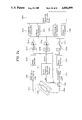
As illustrated in FIG. 1, two half mirrors HM are disposed to form a resonator. Let the light velocity be c, and let the distance between the half mirrors be L. This resonator has a resonant frequency (see FIG. 2) at a frequency interval of c/2L. When light to be measured is rendered incident upon the left half mirror HM, light having the frequency identical to the resonant frequency is transmitted through the half mirror HM and falls on receiving device PD. When half mirror HM is oscillated by means, for example, of a PZT or the like, in order to sweep the resonant frequency, the spectrum of the measurement light can be observed from the output from light receiving device PD.
In the optical frequency spectrum analyzer described in (A), however, wavelength resolving power becomes 0.1 nm (equivalent to about 30 GHz) or thereabout; and an absolute accuracy is about 2 nm (equivalent to about 600 GHz). These results are not favorable. On the other hand, the optical frequency spectrum analyzer described in (B) shows results of the limit of frequency resolving power to about several tens of MHz. If the measurement if effected by inputting light having a reference wavelength, the absolute wavelength can be measured. The treatment is, however, very difficult, and accuracy is deteriorated (in connection with degreee of parallelism of mirrors and addjustment of perpendicular incidence, or error in frequency caused by fluctuations of an interval at which the mirrors are disposed). Furthermore, there is a defect in that it is impossible to simultaneously measure laser beams which are being oscillated in a plurality of modes.
Frequency measurement with high accuracy of 1 MHz or less and with high resolving power is required in the field of optical communication s and photo applied mesurements. Hence, the above types of optical frequency spectrum analyzers are unsatisfactory.
FIG. 3 is a block diagram depicting a conventional optical fiber loss wavelength characteristic measuring device. Output light from a variable wavelength light source VL enters a fiber MF to be measured, and the subsequent emergent light is detected by a photo detector PD. The detected light is outputted as an electric signal to an amplifying/displaying circuit DP. The characteristics of wavelength are measured from the variations of light power obtained when sweeping the output wavelength of the variable wavelength light source VL.
FIG. 4 is a block diagram showing a conventional optical fiber wavelength dispersion characteristic measuring device. The variable wavelength light source VL and a reference wavelength light source SL are amplitude modulated by a modulation signal source Ef having a frequency f. The photo detector member PD detects output optical powers both of measurement fiber Mf to which the output light of variable wavelength light source VL is applied and of reference fiber SF to which the output light of source SL is applied. The phase differences in component of the frequency f between the two outputs are detected by a phase measuring device PS, thereby measuring a propagation delay time with respect to the wavelength of the measurement fiber MF.
However, the measuring devices depicted in FIGS. 3, 4 are deficient in many respects, such as, the optical phase propagation characteristics cannot be measured in a highly accurate manner. The only acceptable measurement becomes possible with use of a long light path as in the case of optical fibers. A short waveguide path is not acceptable for obtaining accurate measurements. The measurement in regard to the propagation characteristic (e.g. loss, gain, phase, delay) and reflection characteristics is of importance to testing performance of such devices as the optical fiber, light waveguide path, wavelength branching filters, optical switches and the OEIC which are all essential components in any communication system or photo applied measurement systems. The above described conventional devicees and systems are not sufficiently adequate.
SUMMARY OF THE INVENTION
Accordingly, an object of the invention is to overcome the aforementioned and other deficiencies and defects of the prior art.
Another object is to provide an optical frequency analyzer wherein light relative to incident light is made to fall upon an optical heterodyne detecting member together with frequency swept light outputted from an optical frequency sweeping member; and an electrical signal with a frequency corresponding to the difference between two frequencies is outputted and is then signal processed by a signal processing/displaying member through the intermediary of a filter, thereby making it possible to measure frequency characteristics of a measurement object with high accuracy, high resolving power and high stability.
BRIEF DESCRIPTION OF THE DRAWINGS
FIGS. 1, 2 are diagrams depicting the principles of a conventional optical frequency spectrum analyzer.
FIG. 3 is a block diagram depicting a conventional optical fiber loss wavelength characteristic measuring device.
FIG. 4 is a block diagram depicting a conventional optical fiber wavelength dispersion characteristic measuring device.
FIG. 5 is a block diagram depicting a first illustrative embodiment of the invention.
FIGS. 6(a) and 6(b) is a time chart depicting operation of the embodiment of FIG. 5.
FIG. 7 is a graph depicting operation of the embodiment of FIG. 5.
FIG. 8 is a block diagram depicting a photo amplifying device.
FIG. 9 is a block diagram depicting a second illustrative embodiment of the invention.
FIG. 10 is a block diagram depicting details of a marker attached variable wavelength light source used in the embodiment of FIG. 9.
FIG. 11 is a spectrum chart depicting a marker signal output Em on the basis of frequency regions of the arrangement of FIG. 10.
FIG. 12 is a block diagram depicting a second example of the marker attached variable wavelength light source of FIG. 10.
FIG. 13 is a block diagram depicting a third example of the marker attached variable wavelength light source of FIG. 9.
FIG. 14 is a block diagram depicting a fourth example of a marker light source used in the arrangement of FIG. 9.
FIGS. 15(A), 15(B) and 15(C) are graphs depicting characteristic curves of the device of FIG. 14.
FIG. 16 is a block diagram depicting a fifth example of a marker light source used in the arrangement of FIG. 9.
FIG. 17 is a block diagram depicting a sixth example of a marker light source used in the arrangement of FIG. 19.
FIG. 18 is a graph depicting a characteristic curve of the device of FIG. 17 .
FIG. 19 is a block diagram depicting one example of a tunable laser user in the arrangement of FIG. 10.
FIG. 20 is a block diagram depicting a second example of a tunable laser.
FIG. 21 is a block diagram depicting a third example of a tunable laser.
FIG. 22 is a perspective view depicting a fourth example of a tunable laser.
FIG. 23 is a block diagram depicting one example of a reference wavelength laser light source used in the arrangement of FIG. 10.
FIG. 24 is a block diagram of a third illustrative embodiment of the invention.
FIG. 25 is a block diagram depicting a fourth illustrative embodiment of the invention.
FIG. 26 is a block diagram depicting one example of an optical frequency synthesizer/sweeper used in the embodiments of FIGS. 5 and 24.
FIG. 27 is a block diagram depicting a second example of the arrangement of FIG. 26.
FIGS. 28(A), 28(B) are wave charts showing characteristic curves of the arrangement of FIG. 27.
FIG. 29 is an energy diagram depicting energy levels of Rb gas.
FIG. 30 is a block diagram depicting a third, partially varied, example of the arrangement of FIG. 26.
FIG. 31 is a block diagram depicting a fourth example of the arrangement of FIG. 26.
FIG. 32 is a block diagram depicting another example of the optical frequency synthesizer/sweeper wherein a multiple light source is formed.
FIG. 33 is a graph depicting characteristic curves of the frequency spectrum of the output light of the arrangement of FIG. 32.
FIG. 34 is a block diagram depicting an example of a frequency stabilized semiconductor laser used as a reference wavelength light source.
FIG. 35 is an energy diagram showing a hyperfine structure of the energy level of a Cs atom.
FIG. 36 is a graph depicting optical absorption caused by the Cs atoms.
FIG. 37 is a diagram depicting operation of the arrangement of FIG. 34.
FIG. 38 is a graph depicting the characteristic curve of the arrangement of FIG. 34.
FIG. 39 is a block diagram depicting the principal portions of a second example of a frequency stabilized semiconductor laser.
FIG. 40 is a block diagram depicting the principal portions of an optical system of a third example of a frequency stabilized semi-conductor laser.
FIG. 41 is a block diagram depicting a fourth example of a frequency stabilized semiconductor laser.
FIG. 42 is a graph depicting an output signal from a lock-in amplifier used in the arrangement of FIG. 41.
FIG. 43 is a block diagram depicting principal portions of a fifth example of a frequency stabilized semiconductor laser.
FIG. 44 is a block diagram depicting principal portions of a sixth example of a frequency stabilized semiconductor laser.
FIG. 45 is a block diagram depicting principal portions of a seventh example of a frequency stabilized semiconductor laser.
FIG. 46 is a cross sectional view depicting principal portions of an eighth example of a frequency stabilized semiconductor laser.
FIG. 47 is a diagram depicting operation of the device of FIG. 46.
FIG. 48 is a block diagram depicting a ninth example of a frequency stabilized semiconductor laser.
FIG. 49 is a diagram depicting operation of the device of FIG. 48.
FIG. 50 is a block diagram depicting principal portions of a tenth example of a frequency stabilized semiconductor laser showing a partial modification of FIG. 48.
FIG. 51 is a block diagram of an eleventh example of a frequency stabilized semiconductor laser.
FIG. 52 is a diagram depicting operation of the device of FIG. 51.
FIG. 53 is a block diagram depicting principal portions of a twelfth example of a frequency stabilized semiconductor laser.
FIG. 54 is a block diagram depicting a thirteenth example of a frequency stabilized semiconductor laser.
FIG. 55 is a block diagram of a fourteen example of a frequency stabilized semiconductor laser, in principal portions thereof.
FIG. 56 is a block diagram depicting principal portions of a fifteenth example of a frequency stabilized semiconductor laser.
FIG. 57 is a block diagram depicting a sixteenth example of a frequency stabilized semiconductor laser.
FIGS. 58, 59 are graphs showing outputs of lock-in amplifiers used in FIG. 57.
FIG. 60 is a block diagram of a seventeenth example of a frequency stabilized semiconductor laser.
FIG. 61 is a block diagram depicting an eighteenth example of a frequency stabilized semiconductor laser.
FIG. 62 is a block diagram depicting principal portions of a nineteenth example of a frequency stabilized semiconductor laser.
FIG. 63, FIG. 64, and FIG. 65 are graphs showing Zeeman separation of the energy levels of Cs atom.
FIG. 66 is a perspective view depicting a twentieth example of a frequency stabilized semiconductor laser wherein the device is formed as an integrated circuit.
FIG. 67 is a table depicting a method of fabricating respective components of the device of FIG. 66.
FIGS. 68, 69 are perspective views depicting principal portions of another example of the device of FIG. 66.
FIGS. 70, 71, 72 are cross sectional views depicting principal portions of the device of FIG. 66.
FIG. 73 is a plan view depicting a twenty first example of a frequency stabilized semiconductor laser as laid out on an integrated circuit.
FIGS. 74(A), 75(B), 74(C) and 75 are perspective and plan views showing principal portions of another example of the arrangement of FIG. 73.
FIG. 76 is a block diagram depicting a twenty second example of a frequency stabilized semiconductor laser.
FIG. 77 is a diagram showing operation of the arrangement of FIG. 76.
DETAILED DESCRIPTION OF PREFERRED EMBODIMENTS
In the different figures, the same components having the same function will bear the same reference symbol, in general. Where that is the case, to improve clarity of description, repeated discussion of the component will be generally avoided.
FIG. 5 depicts an optical frequency analyzer which can perform frequency analysis. The belt like arrow head indicates flow of photo or optical signals, while the solid line arrow head indicates flow of electrical signals. The analyzer comprises a polarization control unit 1a which uses a magnetic optical effect crystal (YIG, lead glass or the like) in which measurement light, defining an object to be measured, is arranged to be incident light; a photo amplifying device 2a for for inputting output light from control unit 1a; a local oscillator 3a which constitutes an optical frequency sweeping device; a half mirror HM1a for inputting beams of output light from oscillator 3a and of amplifier 2a; an optical heterodyne detector 4a comprising e.g. PIN photodiode, avalanche photodiode, or the like, for inputting output light from half mirror HM1a; filter 5a having a band pass property for inputting and amplifying electric output from heterodyne detector 4a; a detector for inputting electric output from filter 5a; and a signal processing/displaying circuit 72 for inputting electric output from detector 6a.
Local oscillator 3a comprises a sweeping signal generator 32a, reference wavelength light source 1s, and optical phase locked loop 2s for inputting light output from light source 1s. Loop 2s is arranged such that the frequency sweeping thereof is controlled by signal generator 32s and the output thereof is outputted to half mirror HM1a.
Photo amplifier 2a comprises a GaA1As laser (780 nm zone) and an ImGaAsP laser (1500 nm zone) and may utilize the following types of amplifiers.
(A) A Fabry-Perot cavity type amplifier wherein bias electric current flows in the vicinity of the oscillation threshold value, signal light strikes a laser diode, and linear photo amplification is effected by inductive emission.
(B) An injection locking amplifier wherein signal light strikes a laser diode which continues oscillating, and wherein the optical frequency and the phase of the oscillation are controlled.
(C) A travelling wave type amplifier wherein both end surfaces of a laser diode chip are coated with non-reflective material, and photo amplification is performed by transmission of light.
Operation of the FIG. 5 embodiment is as follows. Local oscillator 3a comprises an optical frequency synthesizer/sweeper, which will be described hereinbelow in greater detail, and which sweeps the wavelength of output from loop 2s by the output from generator 32a. Loop 2s, having output frequency ωo, controls the wavelength of the output such as to correspond to an oscillation wavelength or reference source 1s, having output frequency ωs. With this arrangement, it is possible to output local oscillation light with high accuracy, high stability and high spectral purity.
When measurement light having frequency ωi enters unit 1a, a polarization plane of incident light is arranged to be identical to another polarization plane of the output from oscillator 3a by controlling the impressed magnetic field while utilizing rotary polarization of the magnetic optical effect crystal. The output from control unit 1a is amplified by amplifier 2a and is then synthesized with the output from oscillator 3a by half mirror HM1a . The synthesized light output is converted by heterodyne detector 4a into an electrical signal having a frequency equivalent to the difference obtained by ωoi ' (in this case, however, ωi '=ωi). The electric output from heterodyne detector 4a is partially transmitted through filter 5a by its band pass properties and is taken out as power in detector 6a. The processor/display unit 7a inputs electric output from detector 6a as a power signal and at the same time inputs a signal relative to the sweeping from generator 32a as a frequency axial signal, thereby spectrum displaying the measurement light.
Examples of operating frequencies are wavelength of ωs is 780 nm (wavelength of laser diode locked to absorption line of Rb); wavelength of ωo is 1560 nm±50 nm; and wavelength of ωi is 1560 nm±50 nm. These operational frequency examples are confined to the case where the measurement light has the most suitable wavelength for optical communication. They are particularly effective in the measurement of characteristic (e.g. absolute wavelength, spectrum distribution and spectrum width) of light emitted from a laser diode in a communication system.
FIG. 5, a pulse synchronizing signal is added to generator 32a for the purpose of exhibiting such an example that the spectrum is, with pulse light serving as incident light, measured. FIGS. 6(A), 6(B) time charts are provided to explain the operations of the above case. A trigger signal (see FIG. 6(B)) synchronized with pulse light is inputted to generator 32a oscillator 3a. Synchronized with this, frequency ωo of loop 2s is, as shown in FIG. 6(A), swept in a step configuration. Simultaneously, a signal, identical to that of FIG. 6(A), corresponding to the sweeping of frequency ωo is transmitted to processor/display 72. As a result, a power spectrum of ωo exists at one point for every beam of pulse light and hence it is feasible to output the whole spectrum of pulse light depicted in FIG. 7 after sweeping operation has been completed.
In FIG. 5, the frequency resolving power of the optical frequency spectrum analyzer is determined both by the spectrum width of output frequency ωo of oscillator 3a and the band width of filter 5a. The spectrum width of frequency ωo is likewise determined by the variable wavelength light source of the optical frequency synthesizer. An external resonator type laser diode, which will be discussed later with respect to FIGS. 19-22, is further used, whereby it is possible to obtain excellent frequency resolving power eg 100 KHz.
Moreover, it is feasible to obtain an optical frequency spectrum analyzer which is highly precise, e.g. at 10-12, with absolute wavelength accuracy and which is highly stable.
Furthermore, the light pulse can be easily measured. Also, a W-Ni (tungsten, nickel) point contact diode and a Josephson element can be used for the heterodyne detector 4a. Although, a band pass filter is used as filter 5a, other filters can be used. For example, a low pass filter may be used. In this case, there is detected optical power of ωi ' so that the equation ωi '=ωo is established to accompany sweeping of frequency ωo.
FIG. 8 depicts another example of a photo amplifier 2a. The amplifier 2a comprises a local oscillator OC1a generating an output having frequency ωL which uses a second wavelength stabilized light source; a photo amplifier OAa for inputting output from control unit 1a; an optical frequency mixer OX1a which uses a non-linear type optical crystal for inputting the output from photo amplifier OAa and output from local oscillator OC1a. Due to the non-linear optical effect, the output frequency ωi ' of mixer OX1a is ωi '=ωiL. As the oscillator OC1a, the preferred arrangement is an optical frequency synthesizer/sweeper, such as shown in FIG. 27, which outputs highly accurate frequency ωL. If such a photo amplifier is used, the measurement frequency range will also be expanded except for the sweeping range of ωo. Provided that local oscillator OC1a which is capable of outputting a plurality of frequencies ωL1, ωL2 . . . is used, it is feasible to obtain an even greater sweeping range.
FIG. 9 depicts another spectrum analyzer which differs from FIG. 5 as follows. A marker attached variable wavelength light source 310a is arranged such that the frequency sweeping is controlled by sweeping signal generator 32a in local oscillator 30a that constitutes a sweeper. Half mirror HM2a synthesizes reference wavelength light Rs and variable wavelength light Rv of the marker attached variable wavelength light source 310a. Beams of output light from amplifier 2a and output from half mirror HM2a are synthesized in half mirror HM1a and are then supplied to heterodyne detector 4a. Processor/display 7a inputs signal relative to the sweeping from generator 32a as the frequency axial signal and concurrently inputs electric output from detector 6a as the power signal. After this process, processor/display 7a spectrum displays a beam of measurement light 71a and a beam of reference light 72a and at the same time displays a marker 73a after inputting a marker electrical signal Em outputted from source 310a.
FIG. 10 depicts details of the source 310 of FIG. 9 which comprises an input terminal 11a to which a sweeping electrical signal Ei for controlling the wavelength is applied; a tunable laser 12a for inputting the sweeping electrical signal Ei through the intermediary of input terminal 11a; a beam splitter BS1a for bidirectionally splitting output from tunable laser 12a; a resonator FP1a which constitutes a marker light source, consisting of a Fabry-Perot etalon for inputting light transmitted through beam splitter BS1a; electro-optic element EO1a provided on the optical axis within resonator FP1a; a signal source E1a for driving element EO1a; a light receiving element PD1a for receiving output from resonator FP1a and for converting it to an electrical signal; and a highly accurate and stable reference wavelength laser light source 14a for emitting output light having a substantially constant wavelength.
Operation of the FIG. 10 embodiment is as follows. Laser 12a emits output having a wavelength corresponding to signal Ei which is applied via input terminal 11a. The output is reflected by beam splitter BS1a thereby to become the variable wavelength output Rv. The rest is transmitted through beam splitter BS1a and are then inputted to resonator FP1a. Resonator FP1a is capable of changing its equivalent resonator length by operation of electro-optic element EO1a, since element EO1a is present on the light path. Thus, a beam of output light Rm from resonator FP1a produces a peak value at a wavelength interval corresponding to the output voltage from signal source E1a. Light receiving element PD1 detects output RM and converts it into an electric signal which is outputted as a marker signal Em from terminal 13a. FIG. 11 shows marker signal Em on the basis of frequency regions. Reference source 14a emits output light Rs having a substantially constant wavelength within the scope of the output band of the variable light source 12a.
Operational examples of frequencies are wavelength of reference light Rs is 780 nm (wavelength of laser diode locked to absorption beam of Rb); wavelength of variable wavelength light Rv is 780 nm±50 nm; and wavelength of ωi is 780 nm±50 nm.
In the FIG. 9 embodiment, since the reference light, marker light and measurement data are recorded or displayed, it is feasible to readily ascertain the absolute value of the wavelength, if the number of intervals of marker light is counted from the wavelength of the reference light and at the same time interpolation is effected.
The frequency resolving power of the analyzer is determined by the spectrum width of the variable wavelength light Rv of source 310a and by the band width of filter 5a. Since the spectrum width of the variable wavelength light depends on tunable laser 12 of light source 310a, it is possible to obtain excellent frequency resolving power (e.g. of 100 KHz) by utilizing an external resonator type laser diode which will be explained with reference to FIGS. 19-22. Also, it is feasible to produce an analyzer which is highly accurate and stable at the absolute wavelength (e.g. in the range of 10-12). Moreover, in the FIG. 10 embodiment, if the effective length of the Fabry-Perot etalon FP1a can be freely varied, the electro-optical element EO1a is not needed.
FIG. 12 depicts a variation of the marker attached variable wavelength light source 310a of FIG. 10 and comprises a beam splitter BS2a provided on the output light path for reference source 14a, for causing output light to be reflected and to strike beam splitter BS1a; a lock-in amplifier LA1a for inputting output from light receiving element, which is a detector , PD1a; a bias signal source E2a whose output is added to the output from lock-in amplifier LA1a and is then applied to electro optical element EO1a. Some beams of output light from reference source 14a are reflected by beam splitter BS2a and fall via beam splitter S1a upon resonator FP1a. The resonator length of resonator FP1a is controlled so that the reference wavelength component reaches its maximum in a feedback loop comprising lock-in amplifier LA1a, thereby making it possible to cause the marker light to accord with the reference wavelength.
FIG. 13 depicts details of the marker attached light source 310a for use in the arrangement of FIG. 9, and comprises an absorption cell CL1a which comprises a standard substance, e.g. Cs, for receiving light transmitted through beam splitter BS1a (this absorption cell CL1a constitutes a marker light source); a light receiving element or detector PD1a for receiving output Rm from absorption cell CL1a and converting it into an electrical signal; a comparator CP1a for receiving electric signals from detector PD1a; and a marker signal output terminal 13a connected to comparator CP1a. The standard source may comprise any of Cs (having two absorption beams in the vicinity of 852 nm), Rb (having four absorption beams in the vicinity of 780 nm, and four absorption beams in the vicinity of 794 nm), NH3 (having a a plurality of absorption beams, and H2 O (having a plurality of absorption beams.).
Operation of the FIG. 13 arrangement is as follows. Part of the beams of output from tunable laser 12a is transmitted through beam splitter BS1a and strikes absorption cell CL1a. The incident light is subjected to absorption at a given wavelength by the standard substance and outputted as transmitted light Rm having peak value (i.e. the lowest point) at the stabilized wavelength. Element PD1a converts output light Rm into electrical signals which are waveform arranged. The arranged signal is, as marker signal Em, outputted from terminal 13a. Since quantum standard marker light is outputted, the wavelength can be measured with high accuracy.
FIG. 14 depicts another marker light source used in the source 310a of FIG. 9. The arrangement comprises a light source LL1a having consecutive spectrums (this light source comprises an LED, a xenon lamp or the like); a lens LS1a for causing beams of output light from light source LL1a to be parallel; and a Fabry-Perot resonator FP2a comprising two seim-transparent mirrors, for acting on the output light from lens LS1a.
Operation of the FIG. 14 device is as follows with reference to FIGS. 15(A), 15(B), and 15(C). Source LL1a outputs light having a large width of spectrum as shown in FIG. 15(A). The beams of light outputted from source LL1a are rendered parallel by lens LS1a and further enter resonator FP2a, thereby resonating between the two semi-transparent mirrors thereof. Let the length of the resonator (i.e. distance between the two semi-transparent mirrors) be L1, let the light velocity be c, and let the refractive index be n1. Then, the transmissivity of the resonator, as shown in FIG. 15(B), has a sharp peak for every c/2n1 L1. As a result, the light outputted from the semi-transparent mirror is as shown in FIG. 15(C). Accordingly, a reference marker can be produced with a simple device.
FIG. 16 depicts details of another marker light source for use in source 310a of FIG. 9, wherein the effective length of the resonator of FIG. 14 is varied. The arrangement comprises an electro-optic crystal EO1a incorporated in the light path of the Fabry-Pero resonator FP2a; and a control signal source E1a connected to an electrode of the crystal EO1a. When an electric field is applied to crystal EO1a by control signal source E1a, the refractive index of crystal EO1a changes, whereby the equivalent or effective length of the resonator is varied. Hence, the wavelength of the output light can be readily changed. With a simple arrangement, it is feasible to manufacture an optical frequency marker device wherein using a simple electrical device, the frequency can be varied by varying the effective resonator length.
In each of the foregoing embodiments, the resonator may be placed in a constant temperature oven to control the temperature of the resonator to be substantially constant and produce a stable frequency interval.
FIG. 17 depicts details of a further marker source comprising a semiconductor laser LD1a comprising both ends which are AR-coated with non-reflective material; collimator lens LS2a, LS3a for causing the beams of output from laser LD1a to be parallel; semi-transparent mirrors HM3a, HM4a which form an external resonator disposed outside lens LS2a, LS3a; and an attenuator ATa through which light is outputted from semi-transparent mirror HM4a. The beams of output light transmitted through semi-transparent mirror HM3a coverage at lens LS4a and are then detected by a photo-detector PD2a, which may be an APD (avalanche photo diode). The output electric signal from detector PD2a is amplified by an amplifier A1a, and its waveform is monitored by a spectrum analyzer SAa.
Operation of the FIG. 17 embodiment is as follows with reference to FIG. 18. A gain curve of spontaneous emitted output light from laser LD1a is depicted as indicated by a dotted line (a) in FIG. 18. The beams of light which are outputted from both end surfaces of laser LD1a, respectively, become parallel in lens LS2a, LS3a and resonate between semi-transparent mirrors HM3a, HM4a. Let the length of the resonator be L2, let the light velocity be c, and let the refractive index be n2. Then, the free spectrum range of the external resonator is determined by c/2n2 L2, and as indicated by a dotted line (b) in FIG. 18, Q rises for every c/2n2 L2. Subsequently, the marker output light outputted from attenuator ATa is characterised (i.e. multiple modes oscillation) as shown by the solid line (c) in FIG. 18. The wavelength interval λx of the marker output light can precisely be read as a frequency interval ωx by an electrical spectrum analyzer SAa. If resonator length L2 is varied, it will be possible to change the wavelength interval λx of the marker output light. For example when L2 =10 mm, the frequency interval ωx is given by ωx =c/2L2 =15 GHz. When the external resonator is placed into the constant temperature oven as occasion requires, a stable frequency interval can be obtained.
FIG. 19 depicts details of a tunable laser 12a used in the marker attached variable wavelength light source 30a of FIG. 10, wherein an element having wavelength selectivity is incorporated in the resonator. The arrangement comprises a semiconductor laser LD2a; non-reflection coated surfaces 121a, 122a provided at both ends of the laser LD2a; lens LS5a for causing beams of light emerging from non-reflection surface 121a to be parallel; half mirror HM5a on which light transmitted through lens LS5a is reflected (this half mirror outputs resonant light to the outside); lens LS6a for causing light emerging from non-reflection surface 122a to be parallel; a first acousto-optical modulator UM1a for receiving light which is transmitted through lens LS6a; a second acousto-optical modulator UM2a for receiving light outputted from modulator UM1s; a mirror M1a for reflecting light emerging from modulator UM2a; and an oscillator DR1a for exciting modulators UM1a, UM2a at a frequency F.
The beams of light which emerge from non-reflection surface 121a of laser LD2a are arranged to be parallel in lens LS5a and are then reflected by half mirror HM5a. The reflected beams of light travel back through the light path and strike laser LD2a once again. The beam of light having a frequency fo1 which emerges from non-reflection surface 122a are arranged to be parallel by lens LS6a and strike modulator UM1a. The wavelength of such light varies so as to satisfy given incident and emergent angles with respect to a diffraction grating created by ultrasonic waves, if the wavelength of the ultrasonic wave applied to modulators UM1a, UM2a changes.
When diffraction is being effected, the incident light is subjected to Doppler shift caused by the ultrasonic waves, and the frequency of +1-dimensional diffracted light (the direction of ultrasonic waves is the same as the diffracted direction) becomes fo1 +F. The emergent light from modulator UM1a is diffracted in modulator UM2a once again. In modulator UM2a, the relation between diffraction light--and direction in which ultrasonic waves travel is opposite to that in modulator UM1a; and 1-dimensional diffraction light is therefore present. As a result, the volume of Doppler shift amounts to -F, and the frequency of output from modulator has the relation fo1 +F- F=fo1. The output light from modulator UM1a undergoes Doppler shift in modulator UM2a after being reflected by mirror M1a. The frequency thereof is express fo1 -F, and further becomes fo1 -F+F=fol in modulator UM1a. It reverts back to the original frequency fo1, thereby returning to laser LD2a. Consequently, the resonant state continues. If the wavelength (frequency F) of the ultrasonic wave is varied, it is feasible to sweep the wavelength of the resonant light. The light which has been resonated is outputted via half mirror HM5a to the outside.
FIG. 20 describes a tunable laser having incorporated in the resonator an element capable of controlling the refractive index of light. The arrangement comprises an electro-optic device EO1a, both surfaces of which are coated with non-reflection material and comprises LiNbO3 (niobium acid lithium) or the like and receives output from lens LS6a; and a signal source E2a for controlling element EO1a. The beams of light which have merged from laser LD2a are arranged to be parallel by lens LS6a and one is transmitted to electro-optic device HO1a. The transmitted light travels back through the previous light path after being reflected by mirror M1a and strikes laser LD2a once again. As a result, a resonator can be constructed between half mirror HM5a and mirror M1a. Let the distance, exclusive of a length along the light path for the electro-optic device EO1a, between half mirror HM5a and mirror M1a be L3, let light velocity be c, and let integer be p, and refractive index be n3. Then, oscillation frequency fo2 is
fo.sub.2 =p·c/2(L.sub.3 +n.sub.3 (V))             (1)
Namely, the refractive index n3 can be varied by changing the intensity of electric field applied to electro-optic device EO1a, using electric signals from source E2a, thereby making it possible to sweep ("sweep" can be construed in some instances to mean control) oscillation frequency fo2.
FIG. 21 depicts details of another tunable laser 12a wherein double resonators are shown. The arrangement comprises a beam splitter BS3a for bidirectionally splitting the emergent light from lens LS6a; electro-optic device EO2a upon which light transmitted through beam splitter BS3a falls; mirror M1a on which the emergent light from electro-optic device EO2a is reflected; electro-optic device EO3a for receiving light reflected by beam splitter BS3a; and mirror M2a for reflecting emergent light from device EO3a. Let the lengths, extending along the light path, of the electro-optic devices EO2a, EO3a be l4, l5, respectively; let the refractive index be n4, n5, respectively; let distinace exclusive of length l4 extending along the light path between half mirror HM5a and mirror M1a be L4 ; let the distance, exclusive of length l5, extending along the light path between the half mirror HM5a and mirror M2a be L5 ; and let the integer be q. Then, in this case, the oscillation frequency fo3 is
fo.sub.3 =q·c/2(L.sub.4 +n.sub.4 (V.sub.1)l.sub.4)-(L.sub.5 +n.sub.5 (V.sub.2)l.sub.5)                                (2)
Since the denominator of formula (2) can be made smaller than that of formula (1), it is feasible to increase the variable range of the oscillation frequency as compared with the arrangement of FIG. 20.
FIG. 22 depicts the tunable laser of FIG. 20 arranged on a single semiconductor chip in an integrated circuit, and comprises a laser diode 123a formed of AlGaAs, InGaAsP; a photo amplifier 124a provided at the joined portion of laser diode 123a; a waveguide path type external resonator 125a; mirrors 126a, 127a provided at both ends of laser diode 123a; an electrode 128a provided on the surface of laser diodes 123a such as to correspond to photo amplifier 124a; and electrode 129a provided on the surface such as to correspond to the waveguide path type external resonator 125a. An electric current ILD is supplied to the joint through electrode 128a, and laser beams are emitted to photo amplifier 124a. An electric current IF is supplied via electrode 129a to resonator 125a and the refractive index of resonator 125a is varied, thereby sweeping the oscillation frequency. Let the lengths extending along the joined portion of the resonator 125a and the photo amplifier 124a be l6, l7, respectively; let the refractive indices be n6, n7, respectively; and let the integer be r. Then, oscillation frequency fo4 is
fo.sub.4 =r·c/2(n.sub.6 l.sub.6 +n.sub.7 (I.sub.F)l.sub.7 ) (3)
FIG. 23 depicts details of a reference wavelength laser light source 14a, such as used in the marker attached source 310a of FIG. 10 and comprises a semiconductor laser LD3a; a beam splitter BS4a upon which output light from laser LD3a strikes; an absorption cell CL2a comprising a standard substance, e.g. Cs, and which receives light reflected by beam splitter BS4a; a light receiving detector PD3a upon which light transmitted through cell CL2a falls; a lock-in amplifier LA1a for inputting electric output from detector PD3a and for controlling electric current applied to laser LD3a in response to the electric signals from detector PD3a; and an oscillator DR2a for frequency modulating the electric current applied to laser LD3a and for supplying a phase detecting frequency from lock-in amplifier LA1a. The light transmitted by beam splitter BS4a becomes the output light of the source. The standard substance may also be Rb, NH3 or H2 O.
The output light from laser LD3a is reflected by beam splitter BS4a, strikes absorption cell CL2a and is subjected to absorption by the standard substance therein. The quantity of absorption is detected by detector PD3a and is fed back via lock in amplifier LA1a to the electric current applied to laser LD3a. The output wavelength of laser LD3a is locked to absorption spectral beams of the standard substance, so that a reference wavelength light is produced by the source with high accuracy and high stability.
One method of absorption is using the linear absorption method. In this method, the absorption spectrum becomes relatively large in thickness by virtue of the Doppler shift. The absorption beams having a hyperfine structure which are hidden due to the Doppler shift are detected by saturated absorption spectroscopy (see T. Yabuzaki, A. Hori, M. Kitano, and T. Ogawa, "Frequency Stabilization of Diode Lasers Using Doppler Free Atomic Spectra", Proc. Int. Conf. Laser, 1983). The oscillation wavelength of the laser LD3a is locked to the thus detected absorption beams, whereby much higher stability can be obtained.
An optical frequency synthesizer/sweeper, which will be described hereinbelow, may be used as the tunable laser 12a in FIGS. 10-13. FIG. 24 depicts one such synthesizer/sweeper is depicted. The synthesizer/sweeper 31a sends forth a frequency swept light output (constituting an optical frequency sweeping device), and will be discussed with respect to FIG. 26. A sweeping signal generator is omitted from this FIG. 24 arrangement. The arrangement of FIG. 24 comprises a optical frequency analyzer and comprises the frequency synthesizer/sweeper 31a; an optical heterodyne detecting member 223a for inputting first and second beams of output light from synthesizer/sweeper 31a; filter 224a comprising a band pass filter for inputting electric output from optical heterodyne detector 223a; optical directivity coupler 220a which inputs a first beam of output light from optical frequency synthesizer/sweeper 31a; an emergent terminal 23a from which output light from optical directivity coupler 220a emerges; an object to be measured 210a for receiving output light from emergent terminal 230a; an incident terminal 240a upon which light emerging from object 210a strikes; a polarization control unit 241a which makes use of a magnetic optical effect crystal (YIG, lead, glass or the like) for inputting incident light from incident terminal 240a; a photo amplifier 242a for inputting output from polarization control unit 241a; an optical heterodyne detector 243a comprising a PIN photodiode, avalanche photodiode or the like, for receiving a second beam of output light from photoamplifier 242a and from synthesizer/sweeper 31a; filter 244a comprising a band pass filter for receiving electric output from heterodyne detector 243a and amplifying such signal; an amplitude comparator 245a for receiving electric signals from filters 244a, 224a; a phase comparator 246a for receiving electric outputs from filters 244a, 224a; polarization control unit 231a, similar to control unit 241a, which receives reflected light from the object 210a through coupler 220a; photo amplifier 232a, similar to photo amplifier 242a, for inputting output light from control unit 231a; optical heterodyne detector 233a, similar to detectors 243a, which receives a second beam of output light from photoamplifier 3232a and from synthesizer/sweeper 31a; filter 234a, similar to filter 244a, for receiving electric output from heterodyne detector 233a, and comprising a band pass filter; amplitude comparator 235a, similar to comparator 245a, for receiving electric outputs from filters 234a, 224a; phase comparator 236a, similar to phase comparator 246a, for receiving electric outputs from filters 234a, 224a; and signal processing/displaying unit 250a for receiving electric outputs from phase comparators 236a, 246a.
A first optical heterodyne detector may be considered to comprise heterodyne detectors 233a, and 243a. A first filter device may be considered to comprise filters 234a and 244a. A second optical heterodyne detector may be considered to comprise detector 223a. A second filter device may be considered to comprise filter 224a. A comparison means may be considered to comprise phase comparators 236a, and 246a and amplitude comparators 235a and 245a. A signal processing means may be considered to comprise signal processing/displaying device 250a. The photo amplifiers may be similar to the photoamplifier 2a shown in FIG. 5. Heterodyne detectors 233a, 223a and 243a may be similar to the optical heterodyne detector 4a shown in FIG. 5.
Operation of the FIG. 24 embodiment is as follows. Synthesizer/sweeper 31a frequency sweeps the light output, and outputs it with high accuracy and high stability and high spectral purity. The first light output which is outputted from synthesizer/sweepr 31a is frequency shifted by Δω by an optical frequency shifter (not shown) comprising an ultrasonic modulator, thereby becoming a second light output. The first light output, having a frequency ωo, from synthesizer/sweeper 31a strikes object 210a via coupler 220 and terminal 230a, and the emergent light from the object 210a is inputted via incident terminal 240a to control unit 241a.
Control unit 241a controls an impressed magnetic field by making most of the rotary polarization of its magnetic optical effect cyrstal, and a polarization plane of the input light is thereby arranged to be identical with that of the local oscillation light (second light output). The output from control unit 241a is synthesized with the local oscillation light from synthesizer/sweeper 31a by a half mirror (not shown) after being amplified by photo amplifier 242a. The synthesized output is then converted by heterodyne detector 243a into an electric signal having a frequency equivalent to the difference Δω=(ωo +Δω)-ωo. The electric output from heterodyne detector 243a is partially transmitted through filter 244a due to its band pass filter properties and becomes a reference signal. The first output, having frequency ωo, from synthesizer/sweeper 31a is directly synthesized with local oscillation light having frequency ωo +Δω, by a half mirror or the like, and is then converted into an electrical signal having a frequency equivalent to the difference Δω between the two frequencies by heterodyne detector 223a and outputted to filter 224a.
The electrical signal output which is influenced by the properties of object 210a, from filter 244a and a reference signal, which is not influenced by the properties of object 210a, from filter 224a (see path synthesizer/sweeper 31a, detector 223a, filter 224a) are compared with respect to the amplitudes thereof in amplitude comparator 245a and are further compared with respect to the phase thereof in phase comparator 246a. The electric outputs from amplitude comparator 245a and phase comparator 246a are signal processed by signal processing/displaying device 250a, whereby the propagation characteristics of object 210a are displayed. The reflected light outputted from object 210a via emergent terminal 230a and directivity coupler 220a is likewise consecutively processed in polarization control unit 231a, photo amplifier 232a, heterodyne detector 233a, filter 234a, amplitude comparator 235a, phase comparator 236a, and signal processing/displaying circuit 250a, whereby the reflection characteristics of object 210a are displayed.
When the light waveguide path is an object to be measured, it is feasible to measure wavelength characteristics of the phase difference or the propagation loss of the waveguide path. On the other hand, if an optical fiber is the object to be measured, measurement becomes possible by utilizing the fiber in such a manner that the wavelength characteristics of delay and propagation loss are short. When a laser diode photo amplifier is the object being measured, the wavelength characteristics of amplification gain, phase delay, and the like can be measured. Furthermore, reflection loss at an optical contact point can be measured from the characteristics of the reflected light. Thus, it can be appreciated, that with the invention, it is possible to measure the amplitude, phase and wavelength characteristics and the like in a highly accurate manner. Moreover, it is feasible to readily and simultaneously measure the propagation characteristics (e.g. loss, phase, delay, gain and the like) of the object to be measured and the reflection characteristics thereof.
In the FIG. 24 embodiment, filters 224a, 234a, 244a, comprise band pass filters. However, other filters, such as a low pass filter, can be used. In the latter case, the equation Δω=0 is established.
Operational frequencies used in FIG. 24 are as follows: Wavelength ωs is 780 nm (wavelength of laser diode locked to absorption beam of Rb); Wavelength of ωo is 1560 nm±50 nm; and Frequency of Δω is 100 MHz. These frequencies are the most suitable for optical communication systems, and also effective in the measurement of light communication devices.
In the FIG. 24 embodiment, the reference signal used for the comparison device is obtained using second heterodyne detector 223a and second filter 224a. The invention, however, is not limited to these types of devices. For example, a modulation signal (corresponding to shift frequency Δω) applied to a frequency synthesizer/sweeper 31a may be used. In this case, the configuration can be simplified by omitting heterodyne detector 223a and filter 224a.
The light which emerges from the network analyzer and travels to the object 210a is not limited to continuous light but may comprise pulse light. It is also feasible to measure the wavelength characteristics with respect to a pulse light by sweeping the optical frequency while synchronizing with the pulse light.
FIG. 25 describes a further analyzer similar to FIG. 24 except that a frequency sweeping device comprising marker attached variable wavelength light source 310a, similar to that used for the spectrum analyzer of FIG. 9, is used instead of synthesizer/sweeper 31a. A sweeping signal generator also is omitted. As with the FIG. 24 embodiment, a first variable wavelength output supplied from source 310a is frequency shifted by Δω by an optical frequency shifter (not shown) thereby forming a second light output. Marker signal output Em from source 310a is inputted directly to signal processing/displaying device 250a, whereby a marker is displayed together with the respective characteristics.
The operational frequencies used in FIG. 25 are: Wavelength ωo is 1560 nm±50 nm; and Frequency of Δω is 100 MHz. These frequencies are suitable for optical communication and measurement.
The FIG. 25 embodiment is simple and can precisely measure various frequency characteristics, such as phase, amplitude, and the like, using a simple variable frequency light source and by correcting the wavelength with use of a marker. In the embodiment, the second light output from variable source 22s (see FIG. 26) may be used as an input light for the optical frequency marker.
An example of the synthesizer/sweeper used in FIGS. 5, 24, is depicted in FIG. 26, and comprises reference wavelength light source 1s in which wavelength is stabilized; optical phase locked loop 2s for receiving light output from source 1s; photo modulator 3s for modulating output from loop 2s; and photo amplifier 4s for amplifying output from modulator 3s. Phase locked loop 2s comprises an optical heterodyne detector 21s which receives light, as an input at one side, from source 1s; variable wavelength light source 22s wherein the oscillation wavelength of output light is controlled by an electric output from heterodyne detector 21s; frequency shifter 23a for shifting the frequency of output from light source 22s; and optical frequency multiplier 24s for multiplying the frequency of output from shifter 23s and for supplying the output thereof as an input to the other side of heterodyne detector 21s.
Operation of the embodiment of FIG. 26 is as follows. When output from reference source 1s is inputted to loop 2s, loop 2s fixes, i.e. locks, the wavelength of the output to one corresponding to the oscillation wavelength of reference source 1s. To be specific, heterodyne detector 21s makes a comparison between the output light emitted from source 1s and output from multiplier 24s, and controls source 22s so as to diminish the difference between the two. Shifter 23s, in a feedback circuit, adds an offset frequency to the output light from source 22s. Multiplier 24s determines the ratio of frequency of output from source 1s to the frequency of output from source 22s. Modulator 3s modulates the output from loop 2s using another signal applied thereto. Amplifier 4s amplifies the output from modulator 3s and supplies the output as an output from the synthesizer/sweeper.
FIG. 27 depicts greater details of the components of FIG. 26 wherein light source 1s comprises a laser diode LD1s; absorption cell CL1s for receiving output light from laser diode LD1s and comprising Rb gas or Cs gas as the standard substance half mirror HM1s upon which output light from cell CL1s falls, photo diode PD1s for inputting light reflected by half mirror HM1s; control circuit A1s for inputting electric output from photo diode PD1s and for controlling electric current applied to laser diode LD1s by an output corresponding to the electric signal from PD1s; a returning light preventing isolator IS1s through which light transmitted through half mirror HM1s passes; and photo amplifier OA1s to which light penetrating isolator IS1s is inputted.
Phase locked loop 2s comprises half mirror HM2s to which is applied output from source 1s; photodiode PD2s comprising a PIN photodiode, avalanche photodiode, or the like, for inputting light transmitted through half mirror HM2s (photodiode PD2s constitutes heterodyne detector 21s); an oscillator ECs which generates an electric signal having a predetermined frequency by inputting reference frequency from a crystal; an a mixer circuit MX1s to which both the electric output from oscillator ECs and electric output from heterodyne detector PD2s are connected and having an output supplied to source 22s.
The variable wavelength light source 22s comprises frequency modulating circult FCs to which is applied output from mixer MX1s; tunable laser diodes VL1s, VL2s, VL3s for receiving outputs from frequency modulating circuit FCs; isolators IS2s through which fluxes of output light from diodes VL1s, VL2s, VL3s pass (isolators IS2s comprise YIG, for example); and an optical switch OS1s for receiving respective outputs from isolators IS2s.
The loop 2s further comprises half mirror HM3s upon which the output from switch OS1s strikes; photo amplifier OA2s for receiving output light reflected by half mirror HM3s; an ultrasonic modulator UM1s for receiving output light from photo amplifier OA2s (modulator UM1s constitutes the optical frequency shifter 23s); light waveguide path NLs comprising a non-linear material, for receiving output from shifter 23s (path NLs constitutes the frequency multiplier 24s); and photo amplifier OA3s for amplifying the output from path NLs.
Photo modulator 3s, which receives output from loop 2s, comprises amplitude modulator AM1s and phase modulator PM1s, both comprising electro-optical crystals, such asLiNbO3 ; polarizing modulator LM1s which uses a magneto-optical crystal such as YIG. Photo amplifying member 4s comprises photo amplifier OA4s and amplifies the output from photo modulator 3s.
Operation of the FIG. 27 embodiment is as follows. Source 1s, as will be described later, controls the oscillation wavelength of laser diode LD1s to absorption beams of Rb or Cs atoms, for example, thereby producing high accuracy and high stability (e.g. at more than 10-12) at an absolute wavelength. If the wavelength of the output from laser diode LD1s, when passing through absorption cell CL1s, accords with the absorption beams of Rb gas (or Cs gas), the output from diode LD1s is absorbed. The absorptive properties are shown in FIG. 28(A).
FIG. 29 depicts an energy level diagram of Rb gas. The absorption beams of Rb are such that a D2 beams is 780 nm and a D1 beam is 795 nm. If the beams are multiplied, the results become 1560 nm and 1590 nm, respectively. These numeric values fall within a zone of 1500 nm which is preferred for optical communications, and for photo applied measurements.
Some fluxes of output from cell CL1s are reflected by half mirror HM1s and are then detected by photo detector PD1s. Thereafter, the output wavelength from laser diode LD1s is locked to the center of absorption by controlling the electric current applied to laser diode LD1s in control circuit A1s such as to correspond to the output from photodetector PD1s. For example, when the output wavelength is to be locked to a point as of FIG. 28(A), it is fixed to a point bs (value of differential waveform becomes zero) of FIG. 28(B) which is a differential waveform of FIG. 28(A) in control circuit A1s by using a lock-in amplifier. This is referred to as the "linear absorption method". According to this method, the absorption spectrum becomes wide as in the case of FIG. 28(A). However, absorption beams of a hyperfine structure, which are concealed on account of Doppler shift, are detected by "saturated absorption" spectroscopy, and if the oscillation wavelength of laser diode LD1s is locked to the detected absorption beams, still higher stability is obtained.
Laser diode LD1s can be stabilized in temperature by use of a constant temperature oven. The light transmitted by half mirror HM1s strikes isolator IS1s. Isolator IS1s prevents light returned from the outside by reflection from changing into noises. The output from isolator IS1s is, as occasion arises, amplified by photo amplifier OA1s.
Loop 2s locks the oscillation wavelength of variable source 22s to the oscillation wavelength of reference source 1s at a predetermined offset and ratio. The output from source 1s passes through half-mirror HM2s and falls upon photo diode PD2s of heterodyne detector 21s. Light fed back from multiplier 24s is amplified by photo amplifier OA3s and reflected by half mirror HM2s and then strikes photo diode PD2s. Let the frequency of output from source 1s and the optical frequency of feedback light be ωs and ω1, respectively, and let the frequency ω2 of output electrical signal from heterodyne detector 21s be given by ω2 =|ωs1 |. Then, provided that the frequency of output from oscillator ECs is ω3, the output ω4 of mixer MX1s (which is a phase detecting circuit) is expressed ω423, when the offset frequency is added to the output frequency ω2 of heterodyne detector 21s. Output electrical signal ω4 of mixer MX1s is inputted to frequency modulation circuit FCs of variable source 22s, and circuit FCs controls the optical frequencies of tunable laser diodes VL1s, VL2s, VL3s, so that the equation ω4 =0 is established.
In connection with the diodes VL1s, VL2s, VL3s, since a resonator is constituted by making the most of the reflection on a diffraction grating incorporated in a diode chip and the oscillation frequency is determined by the pitch of the diffraction grating, there may be used a DFB (distributed feedback) laser and an ADFB (acoustic DFB) laser which is classified as kind of DBR (Distributed Bragg Reflector) (see Yamanishi, M, et. al, "GaAs Acoustic Distributed Feedback Lasers", Jpn. J. Appl. Phys., Suppl. 18-1, P. 355, 1979). These lasers have comparatively stable wavelengths. The ADFB laser generates a surface elastic wave (SAW) such as to be orthogonal to the diffraction grating provided within the DBR laser, and forms an optical ring resonator based on Bragg diffraction which requires the diffraction grating which is incorporated in the chip and the surface eleastic wave. When sweeping the wavelength of the SAW, the resonant wavelength of the ring resonator varies, thereby making it possible to sweep the oscillation wavelength.
In this embodiment, the oscillation wavelength falls within a zone of 1560 nm. The DFB laser, the DBR laser and the ADFB laser which individually include a lengthy resonator have advantages in that the oscillation spectrum is narrow, and the spectrum has good purity. Where the variable wavelength range of a single ADFB laser is insufficient, a plurality of ADFB lasers (VL1s, VL2s, VL3s), may be used, as shown in FIG. 27, whereby it is feasible to perform change-over operation with the aid of an optical switch or light wave synthesizer. Namely, the fluxes of output light from diodes VL1s, VL2s, VL3s are inputted via isolators IS2s to optical switch OS1s, wherein light having a desired variable wavelength range is selected. The fluxes of output light from switch OS1s is partially reflected by half mirror HM3s and are then inputted to photo amplifier OA2s.
The output from amplifier OA2s is inputted to shifter 23s and applied to modulator UM1s, thereby outputting Bragg's s-dimensional diffracted light. Let the frequency of ultrasonic signals supplied from a reference frequency source, such as a crystal oscillator, be ω5, and the optical frequency of the diffracted light shifts be s 107 5.
The output from shifter 23s strikes multiplier 24s, and a secondary higher harmonic wave of the input light is outputted at waveguide path NLs. The tunable laser diode output of 1560 nm is inputted through photo amplifier OA2s, and a signal of 780 nm of a secondary higher harmonic wave is outputted. As a waveguide path NLs, there is used a slab light waveguide path having a quadruple layer of air-TiO2 -ZnS-glass wherein a non-linear thin film of ZnS and a linear thin film of TiO2 are used in order that non-linear effects are produced with high efficiency. In this embodiment, the secondary higher harmonic wave is utilized; however, discretionary n-dimensional higher harmonic wave may also be used.
The output from multiplier 24s is amplified by photo amplifier OA3s. Thereafter, at half mirror HM2s the output light from multiplier 24s is, as the feedback light, brought into confluence with output from source 1s.
In the FIG. 27 embodiment, the optical frequency ωo of output loop 2s is
ω.sub.o =(ω.sub.s ±ω.sub.3)/n±sω.sub.5 (4)
(the symbols are not in the same order). In this embodiment, the optical frequency multiple n is 2. That is, ωo is, at the predetermined ratio of n, locked to optical frequency ωs which assumes high accuracy and high stability at the absolute wavelength, and has an offset of an arbitrary frequency ω3 /n or just ω5. If ω3 or ω5 is swept, it is possible to realize highly accurate sweeping of optical frequency. Since ω3 and ω5 are electrical signals, high accuracy and high stability can be readily obtained.
The output from loop 2s is inputted to modulator 3s and is amplitude modulated by means of an amplitude modulator AM1s. It is further modulated in phase by a phase modulator PM1s, and is then varied with respect to the direction of polarization by a polarization modulator LM1s. After light output from modulator 3s is amplified by amplifier OA4s of photo amplifier 4s, the amplified output becomes the output of the synthesizer.
In FIG. 27 amplifier OA1s to OA4s are the same as those utilized in amplifier 2a of FIG. 5. Also, the positions of shifter 23s and multiplier 24s may be interchanged. The frequency ωo of output from loop 2s may be
ω.sub.o =(ω.sub.s ±ω.sub.3 ±sω.sub.5)/n (5)
In loop 2s both mixers MX1s and shifter 23s are designed for adding offset frequencies, and any one of them may be omitted. Moreover, loop 2a may have its multiple n be 1, in which case, the multiplier 24s may be omitted. Furthermore, although the absorption beams of Rb of Cs are used in absorption cell CL1s of source 1s, other standard substances may be used, such as NH3 or H2 O. Since the discretionary beams (1500 nm zone) of NH3 are highly accurate and stable at the absolute wavelength, multipler 24s may be omitted in that case. Also, it is feasible to stabilize the wavelength by using a Fabry-Perot resonator as a wavelength detector. However, utilizing absorption beams that are standard in terms of quantum is superior to using such Fabry-Perot resonator.
The tunable laser diodes VL1s,VL2s,VL3s are not limited to the ADFB laser used in the embodiment. For example, an external resonator may be used which adopts the diffraction grating added to the outside of the laser diode chip with the diffraction grating being made to rotate, and a variable wavelength is obtained by making the most of its wavelength selectivity. A narrow spectrum is characteristic of such external resonator type laser diode. As another example, the devices of FIGS. 19-22, may be used.
Also, a W-Ni(tungsten-nickel) point contact diode and the Josephson element can be applied to the heterodyne detector 21s. These elements can both multiply and mix. Hence, it is possible to concurrently input ωs, ω1, ω3, thereby making unnecessary the mixer MX1s of FIG. 27. In this case, the outputs from these elements, viz., the frequencies of input signals to circuit FCs become ω4s1 +mω3 (m being a multiple). The equation ω4s -2ω1 ±mω3 is also possible. In that case, multiplier 24s is not required.
FIG. 30 depicts details of heterodyne detector 21s (of FIG. 27) which comprises local oscillator OLs of a optical frequency ωL which utilizes a second wavelength stabilizing source; an optical frequency mixer OXs to which output from oscillator OCs and multiplier 24s are inputted via photo amplifier OA3s (this mixer comprises non-linear optical crystal); and a photo detector ODs comprises a PIN diode, an avalanche photo diode, or the like, for receiving output from mixer OXs and output from reference source 1s and for outputting electrical siganls to variable source 22s.
According to FIG. 30, by virtue of non-linear effect, the optical output frequency ω6 of mixer OXs is expressed as ω61L. In the embodiment of FIG. 27, there is limitatively obtained only ω1 which is to be determined by ωs1 =nωo (apart from the offset frequency) by multiplier 24s. In the embodiment of FIG. 30, however, it is possible to output light with many different wavelengths. For example, when the wavelength λs of ωs is so selected as to be 780 nm by using the absorption beam of Rb and when the wavelength λL of ωL is so selected as to be 852 nm by using the absorption beam of Rb, since there is the relation 1/λs =1/λ1 +1/λL between the respective wavelengths λs, λ1, λL of ωs, ω1, ωL because the relation ωs6 that is valid in time of a feedback loop balance, the equation λ1 =9230 nm is obtained.
FIG. 31 describes an embodiment similar to FIG. 26, but of a synthesizer/sweeper which is capable of simultaneously outputting two optical frequencies. The arrangement comprises a reference wavelength light source 1s and phase locked loop 2s. The source 1s is a two wavelength stabilized laser diode which utilizes saturated absorption method and comprises laser diodes LD11s, LD12s, which generate laser outputs having different wavelengths; half mirror HM4s for causing the outputs from lasers LD11s, LD12s to become confluent with each other; half mirror HM5s for bidirectionally splitting output from half mirror HM4s; absorption cell CL1s (similar to that of FIG. 27) for receiving light transmitted through half mirror MH5s; half mirror HM6s upon which light emerging from cell CL1s strikes; a returning light preventing isolator IS1s through which output from half mirror HM6s passes; mirror M4s which receives light reflected by half mirror HM5s; half mirror HM7s upon which light reflected by mirror M4s falls; diaphragm LS3s for receiving light transmitted by half mirror HM7s; mirror M5s upon which output from diaphragm LS3 s strikes; a photo detector PD11s for receiving output from mirror M5s (as reflected by half mirror HM6s transmitted through cell CL1s and reflected by half mirror HM5s); photo detector PD12s for receiving light reflected by half mirror MH7s and transmitted through absorption cell CL1s; differential amplifier A2 s for computing the difference between an electric output from photo detector PD11s and an electric output from photo detector PD12; lock in amplifiers LA1s, LA2s (which serve as driving circuits for laser diodes LD11s, LD12s) for receiving outputs from differential amplifier A2s and applying outputs to laser diodes LD11s, LD12s, respectively; and a returning light preventing isolator IS1s through which output light from half mirror HM6s passes.
Optical phase locked loop 2s is similar to FIG. 27, but differs in the following respects. Mixers MX11s, MX12s are provided for inputting an electric output from heterodyne detector 21s and FM modulation frequencies ΩA, ΩB. The variable source 22a comprises frequency modulation circuits FC1s, FC2s (which have LPF properties) for receiving outputs from mixers MX11s, MX12s; tunable laser diodes VL4s,VL5s, the oscillation frequencies thereof being controlled by the outputs from circuits FC1s, FC2s; returning light preventing isolators IS21s, IS22s for receiving outputs from respective tunable laser diodes VL4s, VL5s and preventing reflected light from becoming noise; and light wave synthesizer OS2s for inputting and synthesizing light outputs from isolators IS21s, IS22s. The other components are the same as that of FIG. 27.
The operation of the FIG. 31 embodiment is as follows. Provided that the outputs from diodes LD11s, LD12s are ωAA, ωBB, the two fluxes of light are synthesized in half mirror HM4s and are bidirectionally split by half mirror HM5s. The light transmitted through half mirror HM5s is supplied as saturation light to cell CL1s. Thereafter, the light is transmitted through half mirror HM6s and is then outputted via isolator IS1s to loop 2s.
On the other hand, light reflected by half mirror HM5s is further reflected by mirror M4s and is then split bidirectionally by half mirror HM7s. Light passing through half mirror HM7s is diaphragmed by diaphragm LS3s and is reflected by half mirror HM6s. The reflected light becomes probe light which is much narrower than the saturation light and is supplied to absorption cell CL1s. Then, the light is subjected to absorption accompanied with a sharp cavity formed in Doppler expansion by the saturation effect, is reflected by half mirror HM5s and strikes photo detector PD11s. Light that is reflected by half mirror HM7s, serving as reference light, is applied from a perpendicular direction to cell CL1s and then undergo absorption coupled with Doppler expansion.
Subsequently, the light is supplied to photo detector PD12s. Differential amplifier A2s computes the difference between electric outputs from photo detectors PD11s, PD12s and then supplies a difference signal to lock-in amplifiers LA1s, LA2s. With ΩA serving as the reference frquency, lock-in amplifier LA1s effects synchronizing rectification, detects ΩA components alone and controls laser diode LD11s, thereby locking it, for example, to absorption beams of F=1 of FIG. 28, to the center of anyone of absorption beams r to t shown in FIG. 29, which are respectively possessed of a hyperfine structure, the absorption beams being hidden by the Doppler shift.
Similarly, with ΩB serving as the reference frequency, lock-in amplifier LA2s effects synchronizing rectification, detects ΩB components alone and controls the laser diode LD12s, thereby locking it, for example, to absorption beams of F=2 of FIG. 28, to the center of any one of the absorption beams o to q shown in FIG. 29, which individually have hyperfine structures and are concealed by Doppler shift.
Thus, there is produced a two wave length stabilized light source having oscillation frequencies ωAA, ωBB. Two wavelength outputs from source 1s are inputted to loop 2s and are heterodyne detected by heterodyne detector 21s together with output from multiplier 24s. As a result, there are obtained detecting outputs with such frequencies as |ωA1AA |, |ωB1BB |, |ωA -ωA+ΩAB |, |ωA1BA |, |ωB1AB | (wherein ω1A, ω1B are the frequencies of outputs from multiplier 24s). During operation of loop 2s, ωA ≈ω1A, and ωB ≈ω1B. Since ΩA, ΩB are several KHz and the difference between ωA and ωB is, as shown in FIG. 29, 6.8 GHz, it is feasible to take out only the frequency components of |ωA1AA | and |ωB1BB | by imparting low pass properties to photo detectors PD2s. The mixers MX11s, MX12s mix the outputs from heterodyne detector 21s and input signals having frequencies ΩA and ΩB, thereby generating output signals ω4A =|ωA1A |; ω4B =|ωB1B |.
In variable source 22s, the frequency modulation circuits FC1s and FC2s respectively control oscillation frequencies of variable wavelength diodes VL4s, VL5s so that the frequencies of the output signals ω4A and ω4B from mixers MX11s, MX12s come to zero. The light outputs from laser didoes VL4s, VL5s are supplied via isolators IS21s, IS22s, to synthesizer OS2s wherein the outputs are synthesized, thereby generating light outputs having two optical frequencies of ωA /n+sω5, and ωB /n±sω5. These light outputs are not frequency modulated at frequencies ΩA, ΩB.
Although the FIG. 31 synthesizer/sweeper generates two frequencies, more than two frequencies can be generated as desired. Also, although the saturation absorption method is used, linear absorption method can also be used wherein the two wavelengths locked to the center of absorption of F=1 and F=2 are shown in FIG. 28. In the latter case, the incident light to cell CL1s is arranged to be two fluxes of light and two lock-in amplifiers are used as components of the reference source 1s depicted in FIG. 27.
In FIG. 31, modulator UM1s alone is used for offset and sweeping of optical frequencies. However, frequencies ω3.sbsb.A +ΩA and ω3.sbsb.B +ΩB are available which are obtained by adding shift frequencies ω3A and ω3B thereto instead of input frequencies ΩA and ΩB of mixer MX11s, MX12s. In this case, the two optical frequencies of outputs become (ωA ±ω3A)/n±sω5 and (ωB ±ω3B)/n±sω5, respectively. Hence, it is possible to simultaneously sweep the two frequencies at ω5 and to separately sweep the two frequencies by sweeping ω3A and ω3B, respectively.
As shown in each of the embodiments, the synthesizer/sweeper is capable of locking the light output thereof to the absorption beams of Rb or Cs at the absolute wavelength with high accuracy and high stability and of obtaining a quantum standard (conventional frequency standard uses microwave resonance of Cs (i.e. 9 GHz) or Rb (ie. 6 GHz)) having stability of 10-12 or more.
Since an ADFB laser, comprising a lengthy resonator and an external resonator type laser diode, is used as the tunable laser diode, the Q of the resonator is high, and the width of oscillation spectrum can be diminished. Also, since an optical phase locked loop is used, highly accurate sweeping of optical frequency can be performed.
By using absorption beams of Rb (780 nm, 795 nm) and the multiplication method as well, it is feasible to output with high accuracy and stability, light of the 1500 nm zone, which creates the least photo transmission loss. Thus, the invention is highly practical.
Furthermore, with this embodiment, many different optical frequencies can be outputted. In addition, it is possible to concurrently output a plurality of frequencies and to sweep them separately. Moreover, it is feasible to remove unnecessary FM modulation components from the light outputs. Similarly, in the embodiment of FIG. 27, if frequencies ω3'3 +Ω (wherein Ω is the FM modulation frequency when using a lock-in amplifier) and such signal is inputted to mixer MX1s, such removal can be done.
FIG. 32 describes a synthesizer/sweeper similar to FIG. 27 wherein a plurality of light outputs are generated. The arrangement comprises a reference wavelength light source 1s wherein the wavelength is stabilized; a first stage optical phase locked loop 20s for receiving output light from source 1s; a second stage optical phase locked loop 30s for receiving output from first stage loop 20s; and a third stage optical phase locked loop 40s for receiving output from second stage loop 30s.
First stage loop 20s comprises an optical heterodyne detector 21s comprising PIN photo diode, an avalanche photo diode, or the like, for receiving output light from source 1s, at one side thereof as input; a variable wavelength light source 22s wherein an oscillation wavelength of the output light is controlled by electric output from heterodyne detector 21s; and an optical frequency multiplier 24s, comprising a light waveguide path formed of a non-linear material for multiplying the frequency of output from variable source 22s and at the same time supplying output to the heterodyne detector 21s at its other side as an input.
Each of the second stage and third stage loops 30s,40s comprises heterodyne detectors 31s,41s (similar to detector 21s) for receiving part of the output light, as an input at one side, from prior stge loops 20s, 30s; mixers 34s,44s for receiving electric outputs from respective heterodyne detectors 31s, 41s, as input at one side, and a reference offset signal Ax at the other side (reference offset frequency circuit 10s comprises an oscillator for generating electric output AS with a given frequency); and variable wavelength light source 32s, 42s (similar to source 22s) for receiving outputs from mixer 34s, 44s and for supplying part of the output light to heterodyne detector 31s, 41s, as the inputs thereof at the other side, and outputting another part as output light fo1, fo2 of the embodiment.
Operation of the FIG. 32 embodiment is as follows. When output from source 1s is inputted to the first stage loop 20s, loop 20s controls (i.e. locks) its light output wavelength such as to correspond to the oscillation wavelength of source 1s. The output light from variable source 22 is supplied to multiplier 24s which outputs a secondary higher harmonic wave of input light on a light waveguide path formed of non-linear material. Heterodyne detector 21s outputs an electric signal (i.e. a beat signal) having a frequency equivalent to the difference between the frequency of the output light from reference source 1s and the frequency of the output from multiplier 24s. Variable source 22s controls the frequency of output light so that frequency of electric signal from detector 21s becomes zero. Namely, the output frequency from source 1s is equalized to that of multiplier 24s. Taking the results thus far obtained into consideration, let the frequency of the output from reference source 1s be fs, and output frequency fo1 of output from variable source 22s be
fo.sub.1 =(1/2)fs                                          (6)
As far as this embodiment is concerned, the secondary higher harmonic wave is utilized in multiplier 24s. However, when an arbitrary n-dimensional higher harmonic wave is used, it is feasible to obtain the output frequency reduced by a factor of n.
Since the frequency offset frequency fos of reference offset circuit 10s is added to the frequency of the output from heterodyne detector 31s, the frequency of the output light from variable source 32in the second stage loop 30s is
fo.sub.2 =fo.sub.1 +fos=(1/2)fs+fos                        (7)
Similarly, the frequency of the output from variable source 42s in the third stage loop 40s is
fo.sub.3 =fo.sub.2 +fos=(1/2)fs+2fos                       (8)
Namely, as shown in FIG. 33, which depicts a characteristic curve of the frequency spectrum, it is possible to precisely generate light output having the frequency interval fos (e.g. 10 GHz) from the respective stages of loops 20s, 30s, 40s of FIG. 32.
Advantageously, with the FIG. 32 embodiment, it is practicable to lock the reference light output thereof to the absorption beams of Rb at the absolute wavelength with high accuracy and high stability, thereby realizing the highly accurate source generating a plurality of output lights. Moreover, the frequency interval between the different light outputs can be controlled in a highly precise manner. In addition, since the respective frequency intervals are narrow and stable, a source of generating a plurality of highly dense optical signals can be realized.
Moreover, since an external resonator type laser diode is used as the tunable laser diode, it is feasible to increase the Q of the resonator and to reduce the width of oscillation spectrum. Furthermore, the absorption wavelength of the D2 line of Rb is 780 nm in the reference source 1s, and this numeric value is multiplied in the first stage loop 20s, thus obtaining 1560 nm. Consequently, light output is generated which is within the 1500 nm zone, which is used in optical communication systems.
In the FIG. 32 embodiment, the offset frequency can be varied by interposing an ultrasonic modulator between the outputs from variable sources 32s, 42s and the inputs to heterodyne detectors 31s, 41s. Also, the multiple of the multiplier 24s may involve discretionary integers. If the multiple is 1, the multiplier 24 may be omitted. In this case, the respective frequencies of the output light are ##EQU1## In this case, the first stage loop 20s may be omitted. Instead, the output from reference source 1s can be used as the first stage output light. Moreover, although identical reference offset frequency fos is added to each stage, a plurality of reference offset frequencies fos1, fos2, which are different from each other may be added thereto for different stages. In addition, although three stages are shown, the number of stages can be altered as desired.
Next will be described different circuit configurations of the reference wavelength light source 1s which may be used in the optical frequency synthesizer/sweeper.
FIG. 34 depicts a frequency stabilized laser which may be used as a reference wavelength light source, and comprises semiconductor laser LD1, a Peltier element PE1 for cooling off or heating laser LD1; temperatuure control means CT1 for controlling the temperature of laser LD1 to a fixed value by driving element PE1; a constant temperature oven TB1 for decreasing fluctuations in temperature by housing laser LD1 and element PE1; a beam splitter BS1 for bidirectionally splitting output from laser LD1; acousto-optic deflector UM1 upon which one flux of light transmitted through beam splitter BS1 strikes (deflector UM1 constitutes a modulation means); an absorption cell CL1 which receives diffraction light output from deflector UM1 (cell CL1 comprises a standard substance, eg. Cs, which absorbs light at a specified wavelength); an optical detector PD1 for receiving light transmitted through cell CL1; an amplifier A1 for inputting output electric signals from detector PD1; a lock-in amplifier LA1 for inputting electric outputs from amplifier A1; a PID controller CT2 which constitutes an electric current control circuit both for inputting outputs from lock in amplifier LA1 and for controlling electric current applied to semiconductor laser LD1; switch SW1 having one end thereof connected to deflector UM1; signal generator SG1 for supplying outputs for causing switch SW1 to be turned ON and OFF at frequency fm (e.g. 2 kHz); and second signal generator SG2, to which the other end of switch SW1 is connected for generating an electric signal having frequency fD (e.g. 30 MHz) which is applied to deflector UM1.
Operation of the FIG. 34 embodiment is as follows. The temperature of laser LD1 is controlled to a fixed value by Peltier element PE1 by control circuit CT1 which obtains temperature detecting signals within oven TB1 and supplies control signals to element PE1. Output from laser LD1 is bidirectionally split by beam splitter BS1. The reflected light becomes output light which is outputted as the reference wavelength light source, for example. The transmitted light is supplied to deflector UM1. Since deflector UM1 is driven by electric signals having frequency fD from signal generator SG2 when switch SW1 is ON, the majority of light having frequency ωo is diffracted and is then subjected to frequency, i.e. Doppler, shift. Light having frequency ωo +fD which is defined as primary diffraction light is supplied to cell CL1. When switch SW1 is in an OFF state, incident light having frequency ωo which is all defined as zero-dimensional diffraction light is supplied to cell CL1. Switch SW1 is driven by a clock having frequency fm which is provided by signal generator SG1. Hence, the light falling on cell CL1 undergoes frequency modulatoon with the modulation frequency being fm and the modulation depth being fD.
FIG. 35 depicts energy levels of Cs atoms, wherein when light having a wavelength of 852.112 nm impinges on Cs atoms, carriers are excited from 62 S1/2 to 62 P3/2, and the light loses its energy, whereby absorption takes place. In this case, the levels of 62 S1/2 and 62 P3/2 have two or four hyperfine structures respectively. Strictly speaking, absorption thus occurs with respect to light having six types of wavelengths or frequencies between these levels. In fact, however, since the absorption spectrum width is several hundred MHz because of the Doppler expansion, no hyperfine structure having the level of 62 P3/2 can usually be observed. Consequently, as shown in FIG. 36, it is observed that two kinds of absorption (a),(b) are present on the absorption spectrum line. Point (a) of the absorption signals shown in FIG. 36 involves the one sent from F4 and bundle (a) in FIG. 35, while point (b) depicted in FIG. 36 involves the one sent from F3 and bundle (b) shown in FIG. 36.
When light modulated by deflector UM1 falls upon absorption cell CL1, as depicted in FIG. 37, the signal appears in the output by transmitted light volume being modulated at the position alone (e.g. (a) of FIG. 36) of the absorption signals. Provided that this signal is converted into an electric signal by detector PD1 and the converted signal is then synchronously rectified at frequency fm in lock-in amplifier LA1 with aid of amplifier A1, there is obtained a primary differential waveform such as shown in FIG. 38. If the output of lock-in amplifier LA1 is locked (i.e. controlled) to the center of the primary differential waveform, the output light from laser LD1 will have the stable frequency of ωs -fD /2.
According to the FIG. 34 embodiment, since the oscillating fequency of the laser is not modulated, the light source has high stability for instantaneousness of frequency variations.
Even if the diffraction efficiency of deflector UM1 is varied, an optical component (i.e. zero dimensional diffraction light) which does not contribute to the modulation increases in volume, whereas the signal intensity merely decreases; and no influence is exerted on the central wavelength.
Although modulation frequency fm is used as the reference frequency of lock-in amplifier LA1, frequencies of odd numbered multiples may also be used. Also, the standard substance used in cell CL1 may be Rb, Cs, NH3 or H2 O. Furthermore, although deflector UM1 is used as the modulation means, a phase modulator which uses an electro-optic element may, for example, be used. This involves, for example, a longitudinal type modulator, a lateral type modulator and a travelling wave type modulator. Furthermore, although wavelength control is obtained by electric current applied to the semiconductor LD1 being controlled by electric signals from the control means, such wavelength control may be obtained by controlling the temperature of the laser.
FIG. 39 depicts another way of controlling deflector UM1, wherein an FM modulator FM1 is controlled by a sine wave generator SG20 (e.g. modulation frequency fm=2 kHz), whereby the acousto-optic deflector UM1 is modulated by sine waves.
FIG. 40 depicts principal portions of an optical system, wherein the output light from laser LD1 is made to twice impinge on deflector UM1. The arrangement comprises a half mirror HM1 designed for bi-directionally splitting output light from semiconductor laser LD1 and causing the reflected light to strike from one direction upon deflector UM1 and mirror M1 which reflects light which is transmitted through half mirror HM1, and causes the reflected light to strike from the other direction on deflector UM1. When switch SW1 is in the OFF state, light which is reflected by half mirror HM1 is transmitted through deflector UM1 and strikes cell CL1 at frequency ωo. When switch SW1 is ON, the light which is reflected by mirror M1 is diffracted by deflector UM1 and strikes absorption cell CL1 at frequency ωo +fD
The FIG. 40 embodiment advantageously has a substantially constant light path within cell CL1. However, where there is used a phase modulator which utilizes an electro-optic element as the modulating means, the necessity does not arise, because the direction of the output light is substantially constant.
FIG. 41 depicts another stabilized wavelength light source, wherein one part of fluxes of emergent light from deflector UM1 is, as pump light, supplied to cell CL1, and the other part of narrow fluxes of emergent light is, as probe light, supplied from the opposite direction to absorption cell CL1, thereby obtaining saturated absorption signals. By virtue of this saturated absorption spectroscopy, the Doppler expansion disappears. Hence, it is feasible to distinguish the hyperfine structure which was previously explained with reference to FIG. 35. Since the output signals from the lock in amplifier LA1, which are based on the hyperfine structure shown in FIG. 42, can be obtained, it is possible to realize a still more stable frequency stabilized semiconductor laser by locking the output to any one (e.g. ω1 of FIG. 42) of the structures.
In FIG. 41, the portion indicated by a dotted line is different from FIG. 34, and comprises beam splitters BS5 to BS9, light receiving detectors PD11, PD2 and a differential amplifier DA1; and the outputs of differential amplifier DA1 are introduced into lock-in amplifier LA1. In such a case, the optical system arrangement of FIG. 40 can be used so that the direction of the output light from deflector UM1 does not vary substantially.
FIGS. 44,45 depict optical systems for enabling multiple passes of output light through absorption cell CL1 thereby to lengthen the effective length of exposure to absorption substance of the output light and hence increase efficiency and stability. In FIG. 43, which shows only a circumferential portion of the absorption cell CL1, there are provided reflection members 1,2 and a light path 3 for the output light from deflector UM1 which light comprises zero-dimensional diffraction light and primary diffraction light. The output from deflector UM1 passes through the cell CL1 and is then reflected by reflection member 2. The reflected light penetrates absorption cell CL1 once again and is similarly reflected by reflection member 1. After passing through absorption cell CL1, the output light strikes photo detector PD1. Since light penetrates cell CL1 three times, even if the length of the cell is reduced by a factor of three, the volume of absorption is the same. Or to put it another way, with the same absorption cell length, absorption is three times that for light passing through only once.
FIG. 44 is similar to FIG. 43, but due to adjustment of dimensions of cell CL1, mirrors 1,2 and angle of light application, there are five passes of light through cell CL1. In the same manner, the efficiency is increased five times, or cell size can be reduced by a factor of 5.
FIG. 45 is similar to FIG. 44, but mirrors 4 are of metallic thin film formed on the surfaces of absorption cell CL1, for example, by vapor deposition or other similar methods. With this arrangement, advantageously, it is possible to further reduce the size of the device.
FIG. 46 is a cross sectional view cut by a plane including the central axis of the cell CL1, in the device of FIG. 34, and comprises vessel 5 forming the absorption cell CL1; incidence plane 6 of light; emergence plane of light 7; sealing port 8; and a central axis 9 of the cell CL1. Both the incidence plane 6 and emergence plane 7 are inclined at an angle θ to a plane perpendicular to the central axis 9.
FIG. 47 shows multiple reflections of light on incident plane 6, wherein a flux of incident light 10 impinges incident plane 6 of vessel 5, travels within vessel 5 as another flux of light 11, and exits as flux of transmitted light 12. Within vessel 5 the light is reflected a plurality of time as fluxes 13. Then, the light is exited when the light strikes at suitable angles the walls of vessel 5 as exited flux of light 14. Since incidence plane 6 is not parallel to a plane perpendicular to the central axis of the vessel 5, the multiple refected light fluxes 13, light flux 14 are reflected and exited in directions different from light flux 10. Thus, the incident light flux 11 and the multiply reflected light flux 13 do not interfere with each other at all; and, furthermore, incident light flux 10, transmitted light flux 12 and multiple reflected exit light flux 14 do not interfere with each other. Thus, no noise is caused by light interference, and hence the intensity of the transmitted light does not fluctuate together with the frequency, thereby producing stability. Although the description is in connection with the incidence plane 6, the same situation applies to the emergence plane 7.
The oblique angle θ varies in accordance with the thickness of the vessel 5, beam diameter of incident light or the like, but 2° to 3° are sufficient in ordinary cases. Vessel 5 is described to be in the form of a circular cylinder, however, it may assume other suitable configurations like angularity. In short, the incident plane and emergent plane are flat, and it is merely required that they be disposed with respect to each other. The incident plane 6 and emergent plane 7 of vessel 5 may comprise light transmissive material, and other portions thereof may be non-transmissive material. Furthermore, the slopes of the incident plane and the emergent plane need not necessarily be on both the inside and outside of vessel 5. It is sufficient that only one be inclined.
FIG. 48 depicts a frequency stabilized laser wherein evanescent absorption of light is utilized, and comprising a single mode optical fiber FB1 which receives output light from semiconductor laser LD1; a fiber coupler CP1 for receiving output light from fiber FB1; another single mode optical fiber FB2 for transmitting one flux of output light from coupler CP1 and exited as output light of the source; a third single mode optical fiber FB3 which receives another flux of output light from coupler CP1; a waveguide passage type acousto-optic deflector UM11 for receiving output light from fiber FB3; a fourth single mode optical fiber FB4 for receiving output light from deflector UM11 and causing ultimately the emission of light to photo detector PD1; and an absorption cell CL11 through which optical fiber FB4 passes. Absorption cell CL11 encloses a standard substance, eg Cs, which absorbs light at a given wavelength. Cladding is removed from fiber FB4 to expose a core portion a within cell CL11 to the standard substance.
Operation of the FIG. 48 embodiment is as follows. The output from laser LD1, which is controlled in terms of temperature, travels via optical fiber FB1 and is then branched off into two directions by fiber coupler CP1. One flux of the branched output is emitted to the outside through fiber FB2. The other flux of output travels via fiber FB3 to and is applied to deflector UM11 whereat the light is modulated. The modulated light travels through fiber FB4 and then penetrates cell CL11. Within cell Cl11, as shown in FIG. 49, there is generated an evanescent wave, that is, at core portion a, the propagation light permeates outside of the core portion a of fiber FB4. An electric field over this portion a mutually acts on circumferential gas, whereby absorption takes place at a specified wavelength. Thus, when the output of fiber FB4 is detected by photo detector PD1, absorption signals are thus procured. As in the conventional case, when feeding the light via lock in amplifier or the like, back to laser LD1, the oscillating frequency of laser LD1 can be controlled to an area in the vicinity of the center of absorption. The FIG. 48 embodiment has the same advantages as those of FIG. 34. In addition, in FIG. 48, the optical system consists entirely of optical fibers. Hence positioning operation is not required. This leads to simplicity of adjustment and enables miniaturization of the device.
Although a single mode fiber is used, the invention is not limited thereto. For example, a multi-mode fiber can be also used.
FIG. 50 depicts a variation of the absorption component 100 of FIG. 48, wherein the saturated absorption method is used. The arrangement comprises a single mode optical fiber FB5 for propagating output light from deflector UM11; a fiber coupler CP2, one end of which is connected to optical fiber FB5; another single mode optical fiber FB6 that is connected to the other end of coupler CP2 and led through absorption cell CL11, wherein a part of the cladding thereof is removed to expose core part b to the standard substance in cell CL11, and out to whereat the end thereof a half mirror coated end surface 15 is provided; a first photo detector PD21 for detecting light transmitted through end surface 15; a second photo detector PD11 for detecting light reflected by end surface 15 of fiber FB6 and transmitted back through cell CL11, coupler CP2, fiber FB7; and differential amplifier A11 for inputting electric outputs from photo detectors PD21, PD11 and for outputting them to lock in amplifier LA1 (e.g. in FIG. 48).
In the FIG. 50 embodiment, output light from deflector UM11 is transmitted through fiber FB5 and coupler CP2 and through fiber FB6. Subsequently, evanescent waves produced outside core portion b which waves, as pump light, saturate the light absorption of the standard substance, e.g. Cs, in the vicinity of the portion b. A major part (e.g. 90%) of light travelling through optical fiber FB6 strikes end surface 15 and strikes photo detector PD21. On the other hand, the remainder (e.g. 10%) of light is reflected by end surface 15 and travels back through fiber FB6 in the reverse direction and its evanescent waves, as probe light, overlap the pump light to bring forth absorption. This probe light is then led through coupler CP2, and fiber FB7 to photo detector PD11. Since the electrical outputs from detectors PD21, PD11 are compared and the difference therebetween obtained by differential amplifier A11, the absorption signals by the Doppler expansion are erased, thereby outputting saturated absorption signals having sharp absorption spectrums to lock in amplifier LA1. Due to a feedback loop, such as shown in FIG. 48, it is feasible to control the oscillating frequency of laser LD1 in a highly stable manner by virtue of peaks of the saturated absorption sepctrums.
In FIG. 50, although end surface 15 is a coated half mirror, other similar arrangements may be used. For example, a half mirror may be interposed between, for example, fibers FB6.
FIG. 51 depicts another frequency stabilized semiconductor laser similar to FIG. 34 and comprising a variable gain amplifier 16 for receiving outputs from amplifier A1 and outputs electrical signals to lock in amplifier LA1; a comparator comprising an inversion (-) input terminal to which is inputted the output from amplifier A1; and a setting power source 18 connected between a non-inversion (+) input terminal of comparator 17 and a common electric potential point. The gain of variable gain amplifier 16 is controlled by comparator 17.
The resonant absorption cell CL1 in the FIG. 51 arrangement is shown in FIG. 52, wherein suppose the frequency of output light from deflector UM1 is positioned at a point P, the amount of transmitted light increases; the output of amplifier A1 is largely deflected in the negative direction; the output from comparator 17 assumes a high level; and the gain of the variable gain amplifier 16 diminishes. Subsequently, a moving point slowly shifts from point P towards the bottom of the resonant absorption, i.e., in the direction of the frequency ωs. Concurrently, the transmitted light decreases in volume, whereas the output from amplifier A1 gradually grows. At a point Q, the output of amplifier A1 becomes higher than the setting power source 18, the output from comparator 17 comes to a low level, and the gain of variable gain amplifier 16 is heightened, whereby the output from laser LD1 is maintained at a point R with high stability.
FIG. 53 depicts a circuit for imparting a plurality of gains to variable gain amplifier 16, for example, of FIG. 51, and which comprises comparators 171,172,173 with the outputs from amplifier A1 being applied to each of the inversion (-) input terminals of comparators 171,172,173 and the outputs of comparators 171,172,173 controlling the outputs from variable gain amplifier 16; setting power sources 181,182,183 connected between non-inversion (+) input terminals of comparators 171,172,173 and ground. When this embodiment is connected to the arrangement of FIG. 51, the outputs from photodetector PD1 are inputted to amplifier A1, and the outputs from variabel gain amplifier 16 are inputted to lock in amplifier LA1. With such a connection, the comparators 171,172,173 individually assume low levels at points S. T. Q. of FIG. 52; and the gain of amplifier 16 gradually rises. With this embodiment, it is possible to stably converge to point R at high velocity. Also, the gain of amplifier 16 may consecutively be controlled by stepwise increase or decrease.
FIG. 54 depicts a frequency stabilized semiconductor laser similar to that of FIG. 51, wherein a secondary differential waveform of amplifier A1 is used as an input of the comparator. In the arangement signal generator SG1 FM modulates SG2 with sine waves or chopping waves. The outputs from amplifier A1 are inputted to lock in amplifier LA2 and to variable gain amplifier 16. Lock in amplifier LA2 is driven by signal generator SG1 which generates an output having an even frequency 2 fm that is twice as high as the modulation frequency of signal generator SG2, whereby it is synchronously rectified. The secondary differential waveform of amplifier A1 is thus to be obtained. The output from lock-in amplifier LA2 is inputted to inversion (-) input terminal of comparator 17 that supplies output to control amplifier 16. The output from amplifier 16 is inputted to lock-in amplifier LA1. Setting power source 18 is connected between non-inversion (+) input terminal of comparator 17 and ground.
According to the embodiments of FIGS. 51, 53, 54, in case the output light from laser LD1 largely deviates from a preset value, there is no probability of the output light wavelength exceeding the preset value, and hence, it is feasible to keep the output wavelength to the preset value with high stability. By virtue of this advantage, even if the output light from laser LD1 greatly deviates from the preset value, it is possible to make it converge at the preset value, and at the same time there is a highly stable wavelength.
In all the embodiments of FIGS. 51, 53, 54, variable gain amplifier 16 is disposed behind amplifier A1. It is, however, possible to place the amplifier 16 at the rear of lock-n amplifier LA1 and PID controller CT2. That is, these elements may be disposed at any place within the feedback loop.
FIG. 55 depicts an oven for controlling the temperature of the absorption cell CL1, and comprises constant temperature oven 19 surrounded by an adiabatic material, the inside of which is provided with absorption cell CL1 and is formed with a path for output light from acousto-optic deflector UM1; a temperature measuring element 20 disposed within oven 19 and heater 22 disposed within oven 19. The output of measuring element 20 is connected to a temperature adjuster 21, whose output is connected to heater 22. The temperature control means may be considered to comprise oven 19, measuring element 20, adjuster 21 and heater 22. The temperature within oven 19 is measured by measuring element 20. Heater 22 is so controlled by temperature adjuster 21 as to keep the temperature within oven 19 substantially constant. The temperature is set to such a value that the volume of absorption is large in accordance with dimensions of the absorption cell, and its secondary differential is at a maximum. When standard substance is Cs, the volume of absorption is small at a temperature of less than 20°, and there exists the most suitable value of secondary differential of the absorption quantity in the vicinity of 40° C.
Even if the circumferential temperature varies, the temperature is kept constant, in FIG. 55. Consequently, there is no variation both in volume of absorption and in amount of secondary differential, and the stability of the wavelength of the output light is not deteriorated at all by fluctuations in the circumferential temperature. Furthermore, temperatures at which to increase the absorption quantity of the absorption cell can be selected regardless of the circumferential temperature and hence it is feasible to obtain comparativly large amounts of absorption with respect to even a small absorption cell, thereby making possible the miniaturization of the device. In addition, it is usable within a wide range of circumferential temperatures.
Although heater 2 alone is used to control temperature, if the temperature to be controlled approximates the circumferential temperature, cooling means may additionally be utilized. Moreover, there may be used in place of heater 22 devices, such as a Peltier element, which are capable of heating and cooling.
The temperature measuring element 20 and adjuster 21 may be be omitted by using in place of heater 22 a PTC thermistor or posistor whose resistance value increases in proportion to the temperature increase.
FIG. 56 depicts another temperature controlling oven similar to FIG. 55 but wherein influences due to outside magnetic field are eliminated. The arrangement comprises as of magnetic plate 23, such as of permalloy or the like covering the inside and outside surfaces of the oven which comprises walls of an adiabatic material which surrounds absorption cell CL1 except for the path for output light from acousto-optic deflector UMI, a temperature measuring element 201 for measuring the temperature around cell CL1, a heater 221 and temperature adjuster 211. The output of measuring element 201 is inputted to adjuster 211, which drives heater 221. The temperature of the air space encompassed by the soft magnetic plates 23 and adiabatic material 24 is so controlled as to be substantially constant by means of the temperature measuring element 201, temperature adjuster 211 and heater 221.
The FIG. 56 embodiment is stable with respect to variations in circumferential temperature, and due to magnetic shielding 23, there is no possibility that the absorption spectrum will have Zeeman split resulting from an outside magnetic field and the frequency of output light be thereby varied, and waveform consequently distorted. Since it is unnecessary for the entire system to be housed in a magnetic shield case, it is possible to reduce the system size and still enjoy the benefits of magnetic shielding applied only to the absorption cell.
In the embodiment of FIG. 56, there are two sheets of soft magnetic plates 23 and a sheet of adiabatic material 24. However, only one sheet of soft magnetic plate 23 may be used, or a plurality of plates may be superposed on each other. In this case, if the thin magnetic plates and adiabatic layers are alternately laminated on each other, magnetic shielding effect is enhanced. Also, where the circumferential temperature does not vary much, heater 221 itself may be omitted.
FIG. 57 depicts a frequency stabilized semiconductor laser wherein a multiplicity of stabilized wavelengths are generated and wherein fluxes of output light from semiconductor lasers LD1,LD2 are split by beam splitters BS1, BS2 and apart of such output is arranged to be the light output of the source. The rest of the split fluxes of light are introduced into acousto-optic deflectors UM1, UM2, respectively. The outputs of UM1, UM2 are combined by beam splitters BS3, BS4 and are then introduced into absorption cell CL1. In cell CL1 is enclosed a standard substance which absorbs laser beams having multiple wavelengths. Standard substance may be, for example, cesium, rubidium, ammonia, or water. A plurality of absorption spectrums are created in the light which is transmitted through cell CL1. The laser beams are transmitted through cell CL1 and are supplied to light receiving detector PD1 and then converted into electrical signals corresponding to the light receiving power. The electric signals are applied to lock in amplifiers LA11, LA12, and then outputted to electric current control circuits CT21, CT22. The electric outputs from control circuits CT21, CT22 are applied to lasers LD1, LD2. Hence, the electric currents to be applied to control lasers LD1, LD2 are prescribed by signals added from respective control circuits CT21, CT22, and the oscillating frequencies of the lasers LD1, LD2 are determined by such electric current values.
An oscillator SG2, frequency fD being 80 MHz, eg, is connected via switches SW1, SW2 to acousto-optic deflectors UM1, UM2. The outputs (e.g. fm1 =2 kHz, fm2 =2.5 kHz) of oscillators SG11, SG12 are connected to switches SW1, SW2. Thus, the oscillating wavelength of light applied to deflectors UM1, UM2 is modulated at frequencies fm1, fm2. The outputs from oscilaltors SG11, SG12 are added to lock-in amplifiers LA11, LA12 and are then synchronously rectified at frequencies fm1, fm2. The control means may be considered as comprising control circuits CT21, CT22 and lock in amplifiers LA11, LA12.
Operation of the FIG. 57 embodiment is as follows, assuming that Cs is used as the standard substance in cell CL1. Output light from laser LD1 is bidirectionally split by beam splitter BS1. Reflected light becomes the output light to be emitted to the outside. Light transmitted through beam splitter BS1 is applied to deflector UM1. As in the case of FIG. 34, output light having frequency ω1 from laser LD1 undergoes frequency modulation in deflector UM1 wherein the modulation frequency is fm1 and the modulation depth is fD. Thereafter, the modulated output light falls on absorption cell CL1. Similarly, output light from LD2 having frequency ω2 is subjected to frequency modulation in deflector UM2 wherein the modulation frequency is fm2, and modulation depth is fD. Then, the modulated output light strikes cell CL1.
If light having frequencies ω1, ω2 is made to penetrate the Cs atoms existing within cell CL1, with respect to the amount of transmitted light, there are obtained absorption signals shown in FIG. 36, which correspond to variations of ω1, ω2. Consequently, the output waveform of lock in amplifier LA11, LA12 take the shapes shown in FIGS. 58,59, wherein the signals (see FIG. 36) from element PD1 are differentiated.
Assuming that light having frequency ω1 is modulated at modulation frequency fm1 and light having frequency ω2 is likewise modulated at modulation frequency fm2, when lock in amplifiers LA11, LA12 are synchronously rectified at modulation frequencies fm1, fm2, respectively, (at this time, fm1, fm2 are set so that formula k·fm1 =m·fm2 (wherein k and n are integers) is established), the influences of light having frequency ω2 are not present in the output of lock in amplifier LA11. Similarly, the influences of light having frequency ω1 are not present in the output of lock in amplifier LA12. Subsequently, the outputs from lock-in amplifiers LA11, LA12 individually take the waveforms depicted in FIG. 58 (for outputs from amplifier LA11) and in FIG. 59 (for outputs from amplifier LA12). If the oscillating frequencies of the lasers LD1, LD2 are controlled by control circuits CT21,CT22 so that the output from amplifier LA11 is at a point A of FIG. 58, and the output from amplifier LA2 is at a point B of FIG. 59, then the laser beams appearing at the outputs have wavelengths of 852.112 nm or thereabouts, thereby obtaining fluxes of light having two wavelengths which differ from each other by 9.2 GHz.
Advantageously, the FIG. 57 embodiment is simple and produces a plurality of stable wavelengths. Where Rb is used instead of Cs, the basic level has a hyperfine structure wherein F=1, F=2. Let the frequency at which absorption is caused from F=1 be ω1, and let the frequency at which absorption is caused from F=2 be ω2, then Δω=Ω12, which is defined as the difference therebetween becomes Δω=6.8 GHz in time of 87 Rb and further becomes Δω≈3 GHZ in time of 85 Rb. When using D1 beams (excitation from level 52 S1/2 to level 52 P3/2 implies 794.7 nm) of Rb and D2 beams (excitation from level 52 S1/2 to level 52 P1/2 implies780.0 nm) of Rb, the formula Δλ=14.7 nm is valid. By passing through Cs and Rb, this expression Δλ==852.1-780 (or 794.7)=72.1 (or 57.4) nm, is established. Moreover, molecular absorption beams of H2 O and HNH3 or the like may be used.
The number of semiconductors is not confined to two. If the number is increased, it can be diversified as to type by combining the above frequencies. In such a case, the acousto-optic deflector, the lock-in amplifier, the oscillator and the electric current control circuit must be proportionally added.
FIG. 60 depicts another frequency stabilized semiconductor laser wherein the Doppler expansion disappears using saturated absorption spectroscopy, wherein it becomes possible to distinguish the hyperfine structure described in FIG. 35. Consequently, there is obtained output signal from lock-in amplifier which is based on the hyperfine structure shown in FIG. 42, so that Δω can further be reduced, depending on the position at which the wavelength is locked. The FIG. 60 embodiment differs from the FIG. 57 embodiment in the portions indicated by the dotted lines. The differences are beam splitters BS5 to BS9, light receiving detectors PD11, PD2, and differential amplifier DA1. The outputs from amplifier DA1 are introduced into amplifiers LA11, LA12. The higher harmonic wave frequency of fm1 or the like can be used as the frequency of a signal to be inputted to lock in amplifier. In this case, if a triplex harmonic wave is used, the bias components of the lock-in amplifiers, such as shown in FIG. 58, disappear.
Where a polarization beam splitter is used in place of the beam splitter of FIG. 57, the output laser beam becomes orthogonal polarized waves. FIG. 61 depicts a stabilizer wherein the laser output wavelength is so varied as to correspond to the input signal. The FIG. 61 embodiment differs from FIG. 34 in that coil CI1 is used as a magnetic field applying means around cell CL1. A wavelength variable input signal Sin is applied to the ends of coil CI1. As in the case of FIG. 34, the output from laser LD1 is controlled to a stable frequency of ωs -fD /2. On applying the wavelength variable input signal Sin to the ends of coil CI1, electric current flows through coil CI1, thereby generating a magnetic field, the magnitude of which corresponds to signal Sin. The magnetic field causes the absorption spectrum of the standard substance within the cell CL1 to have Zeeman separation thereby to vary the absorption wavelength. Accompanied with variations of the absorption wavelength, the output wavelength of laser LD1 which is locked to absorption beam changes. It is therefore possible to change the wavelength of the laser output from beam splitter BS1 with the aid of the signal Sin.
The variable light source of FIG. 61 produces a variable wavelength while keeping a stable state in which the output light is locked to the absorption beam of the standard substance. Also, the embodiment is stable for instantaneousness of frequency variations.
In the FIG. 61 embodiment, coil CI1 is used as the magnetic field applying means. Other arrangements are possible, however, such as a permanent magnet may be used and varied as to distance from the cell CL1 in response to signal Sin.
FIG. 62 depicts (see portion A of FIG. 61) an absorption cell CL1 having a magnetic field applying means, but which uses the saturated absorption method instead of the linear method. In this arrangement, light which has been modulated by deflector UM1 is transmitted through beam splitter BS10, as pump light, to absorption cell CL1. Light which is transmitted through cell CL1 is then reflected by mirror M2 and returns through the previous light path. The returned reflected light, serving as probe light, strikes cell CL1 once again, and is transmitted through cell CL1 and is reflected by beam splitter BS10, whereby the saturated absorption signal is detected by photodetectors PD12. The other functions are the same as those of FIG. 61.
When applying wavelength variable input signal Sin to the ends of coil CI1, as in FIG. 61, the absorption spectrum of the standard substance, e.g. Cs, within cell CL1 causes Zeeman separation, whereby saturated absorption wavelength varies. Referring to FIGS. 63, 64, 65, wherein mF is the energy level at which Zeeman separation occurs by effecting magnetic modulation, there are shown Zeeman separation at the respective energy levels of Cs. FIG. 63 is a diagram showing the characteristic curve of Zeeman separation of a 62 P3/2 excitation of Cs. FIG. 64 is a diagram showing the characteristic curve of Zeeman separation of a level of hyperfine structure F=4 in which the basic state of Cs is 62 S1/2. FIG. 65 is a diagram showing the characteristic curve of Zeeman separation of a level of hyperfine structure of F=3 in which the basic state of Cs is 62 S1/2. For example, if the frequency of the semiconductor laser LD1 is controlled to the absorption spectrum obtained when shifting from F=3 of 62 S.sub. 1/2 to F=2 of 62 P3/2, the absorption spectrum shifts toward lower frequencies at the time of applying the magnetic field to the cell CL1. As a result, the oscillating frequency of laser LD1 concurrently shifts toward the lower frequencies.
In the FIG. 62 embodiment, in addition to the characteristics of FIG. 61, variations in saturated absorption frequency are large with respect to changes in magnitude of magnetic field and hence the sensitivity increases. Since the width of absorption spectrum is large in the device of FIG. 61, as compared to FIG. 62, the output frequency can be controlled to substantially the mean value of the energy levels (e.g. F=3 to 5 of FIG. 63) of the hyperfine structure. Consequently, the sensitivity becomes smaller than this.
FIG. 66 depicts a frequency stabilized semiconductor laser disposed on a single chip in an integrated structure. (called "IC" for integrated circuit). The arrangement comprises a photo integrated circuit (IC) substrate 30 comprising, for example, GaAs or the like, and formed on substrate 30 semiconductor laser LD10; light waveguide path 31 upon which the output from laser LD10 travels; acousto-optic deflector UM10 for receiving output emerging from path 31; a second light waveguide path 32 which receives output from deflector UM10; an absorption cell CL10 which encloses a standard substance, e.g. Cs, which is capable of absorption of light with a specified wavelength and which receives light emerging from path 32; light receiving detector PD10 which receives emergent light from cell CL10; and control device 33 for receiving output electric signal from detector PD10.
Control device 33 comprises a lock-in amplifier LA10 having an input connected to the output of detector PD10; an electric current control circuit CT20 consisting of a PID controller circuit having it input connected to the output of amplifier LA10 and its output connected to an injection electric current input to laser LD10; signal generating circuit (e.g. an oscillator) SG10 with a frequency fm (e.g. 2 kHz) (on of the outputs from generator SG10 serving as a reference signal input to amplifier LA10); and a second signal generating circuit (e.g. an oscillator) SG20 having a frequency fD (e.g. 80 MHz), the output of which is connected to deflector UM10 and being modulated by output from generator SG10.
The embodiment of FIG. 66 operates as follows, and is similar to that of FIG. 34. Advantageously, the embodiment is integrated onto a simple semiconductor chip. Hence, the device can be reduced in size, be mass produced and is easy to adjust.
FIG. 67 is a table depicting a method of fabricating the respective components of the embodiment of FIG. 66. For example, the electric current circuit is of the monolithic construction using a silicon substrate. In other cases, however, a hybrid construction may be fabricated. Further details are shown with respect to FIGS. 68-71. FIG. 68 depicts principal portions of a laser LD10 fabricated on a substrate 30 using monolithic techniques. FIG. 69 depicts principal portions of the device using hybrid techniques. FIG. 70 is a cross sectional view of another example. In FIG. 69, end surface of waveguide path 31 is formed on substrate 30 and is directly radiated with outputs from laser LD10. In FIG. 70, output light from laser LD10 is introduced by a prism into path 71.
FIG. 71 is a cross sectional view of the arrangement of FIG. 66 wherein a recessed portion is formed, by etching or other similar method, in the surface of substrate 30. A glass film 34 is formed on the surface by glass coating or thermal oxidation. Next, a standard substance is placed into the recessed portion. This recessed portion is next covered with a glass plate 35 by fusion-bonding, thus enclosing the standard substance within the absorption member CL10.
FIG. 72 is a cross sectional view showing another absorption cell CL10, which may be formed on the device depicted in FIG. 66, wherein a wave guide path 32 is formed on substrate 30 comprising GaAs or LiNbO3 or the like. By evanescent effect, the standard substance enclosed by cover 36 provided on top of waveguide path 32 is arranged to absorb light from laser LD10 passing through path 32. In this embodiment, there is the advantage that manufacturing is easier since the cell is arranged on top of, rather than, within, substrate 30. The photo detector can be incorporated, by using monolithic or hybrid techniques, into the device.
FIG. 73 is a plan view of a chip having an embodiment thereon having a much narrower spectrum than the arrangement of FIG. 66. The arrangement comprises an IC substrate 30; a light branching device OB1 for branching off a part of the fluxes of outut light from semiconductor laser LD10; a light resonant device FP1 consisting of a Fabry-Perot etalon which receives light from branching device OB1; a second photo detector PD3 which receives light from resonator FP1; and a broad band region amplifier A2 for amplifying electric outpts from detector PD3 and feeding the thus amplified outputs back to an injection electric current for laser LD10.
In this configuration, the broad band amplifier A2 (only roughly shown for simplicity) is provided in control device 330. A resonant curve (position deviating from central frequency) of resonator FP1 is made to accord with an oscillating wavelength of laser LD10. Phase noises contained in output from laser LD10 are detected by detector PD3 after converting them into amplitude modulation signals, and the electric outputs thereof are negatively fed via amplifier A2 (which has a band region that is wider than the width of the spectrum of the laser beam) back to the injection electric current which drives the laser LD10, thereby restraining the phase noises of laser LD10 os as to make the spectrum still narrower. (See M. Ohtsu and S. Kotajima, IEEE Journal of Quantum Electronics, Vol. QE-21, No. 12 December 1985).
FIGS. 74(A), 74(B) depict principal portions of a Fabry-Perot resonator FP1 provided on an IC substrate 300 in the device of FIG. 73. FIG. 74(C) is a plan view of the same portion. In FIG. 74(A), a hole 70 is formed in a part of a waveguide path 61 provided on substrate 300, and two surfaces 81 which partially constitute hole 70 and are disposed vis-a-vis with respect to each other, are coated with reflection films, thus forming a resonator. In FIG. 74(B), the ridges 62, serving as waveguide paths, are so spaced from each other as to be placed in series on substrate 300, and end surface 82 of these ridges 62 which surfaces stand vis-a-vis with respect to each other are formed with reflection films, thus constituting the resonator. In FIG. 74(C), a material having a high refractive index is doped at a part of the path 63 provided on substrate 300, thus forming a resonat device 83.
FIG. 75 depicts a means for adjusting the resonant frequency of the resonator FP1 in the device of FIG. 74(C). In FIG. 75 electrodes 90 are provided on both sides of resonator 83 disposed on substrate 300, and the effective length of the resonator 83 is varied by changing the refractive index of the resonant member 83 using electrice current applied between electrodes 90. Another way of adjusting the resonant frequency is to use a thin film resistance formed in close proximity to the light resonant member provided on the substrate, and to vary the length of the resonator by thermal expansion using heat generated by the thin film resistor. In addition, a ferroelectric substance, defined as a material having high refractive index, is doped, and the refractive index is varied by applying electric field in the same manner as FIG. 75.
In the case of controlling the temperature of the laser LD10, and the light resonator 8FP1 to be at a preset value, the thin film resistances can be used as heaters. In this case, it is desirable that the heaters be disposed as remote as possible from each other so that they do not interfere with each other.
In the embodiments of FIGS. 66 to 75, the linear absorption method is used. However, with suitable changes of the optical system, the saturated absorption method can be used.
FIG. 76 depicts a frequency stabilized laser similar to FIG. 34, and wherein the absorption wavelength of the standard substance is modulated by a magnetic field. The arrangement comprises a coil C I 1 wound on cell CL1, coil CI1 constituting a magnetic field applying means. Light transmitted through beam splitter BS1 falls on cell CL1. Outputs from signal generator SG1 are applied to coil CI1 and lock in amplifier LA1. The electric current is modulated by the coil CI1 at a frequency fm (e.g. 2 kHz) and serves as the reference signal for lock in amplifier LA1. On applying the outputs from generator SG1 to both ends of coil CI1, an electric current, modulated by coil CI1, begins to flow, thereby generating a magnetic field in which the intensity varies at the frequency fm. Corresponding to the variations in this magnetic field, the absorption wavelength of the standard substance within absorption cell CL1 is changed by Zeeman separation. As a result, the laser beams fall upon the absorption cell CL1, signals are present in the output when the amount of transmitted light is, as shown in FIG. 77, modulated only at the position of the absorption signal. It is presumed that the magnetic field is modulated within the scope of 0 to a certain value at frequency fm. Frequency ωs is the absorption frequency when the output electric current is 0. Also, when the magnetic field is 0, and FD is the degree to which the absorption frequency varies in time of the magnetic field being applied. This signal is detected and converted into electric signal by detector PD1 and is then synchronously rectified at frequency fm in lock in amplifier LA1 through amplifier A1, thereby obtaining a primary differential waveform illustrated in the diagram of FIG. 38. As in the case of FIG. 34, if the output of amplifier LA1 is locked, i.e. controlled, to the center of the primary differential waveform, the output of the laser has a stable frequency ωs -fD /2.
According to the FIG. 76 embodiment, no acousto-optic deflector is used and therefore it is possible to obtain non-modulation outputs which exhibit the characteristics of high stability for frequency instantaneousness in a compact device requiring low cost of production. Since a deflector is not used, there is only a small amount of heat evolved and power consumption is reduced. Also, the saturated absorption method can be used in place of the linear arrangement by using the arrangement of FIG. 62 in portion B of FIG. 76. Such an arrangement has the advantage that the saturated absorption spectrum can be varied even in a feeble modulation magnetic field since changes in saturated absorption frequency with respect to variations in magnitude of the magnetic field are large, and the sensitivity to variations in the magnetic field is high.
The foregoing description is illustrative of the principles of the invention. Numerous modifications and extensions thereof would be apparent to the worker skilled in the art. All such modifications and extensions are to be considered to be within the spirit and scope of the invention.

Claims (34)

What is claimed is:
1. An optical frequency analyzer for measuring frequency characteristics of an object on the basis of incident light, said optical frequency analyzer comprising
means for applying incident light to an object;
an optical frequency sweeping means for frequency sweeping light and for outputting frequency swept light of a first frequency;
an optical heterodyne detector means for heterodyning said frequency swept light of said first frequency from said optical frequency sweeping means and light of a second frequency indicative of said incident light, and for outputting an electrical signal having a frequency corresponding to the difference between said first and second frequencies;
first filter means for filtering said electrical signal from said optical heterodyne detector means and for producing an electrical output indicative of the filtered results; and
a signal processing/displaying means for processing and displaying said electrical signal from said first filter means.
2. The analyzer of claim 1, further comprising a polarization control means for controlling the polarization plane of said incident light and for producing an output light indicative thereof; and photo amplifying means for amplifying said output light from said polarization control means and for producing an output light indicative thereof.
3. The analyzer of claim 2, wherein said photo amplifying means comprises a photo amplifier for producing an amplified output light; a source for generating a wavelength stabilizing light; and an optical frequency mixer for mixing said wavelength stabilizing light from said source and said amplified output light from said photo amplifier.
4. The analyzer of claim 1, further comprising detecting means for detecting said electric output from said first filter means and for producing an output; means for measuring an optical frequency spectrum of said incident light; and means for causing said output from said detecting means to be an optical power input to said signal processing/display means and for causing an electrical signal indicative of said swept light from said optical frequency sweeping means to be a frequency axial input to said signal processing/display means.
5. The analyzer of claim 4, further comprising means for generating a periodic pulse light; means for causing the frequency of said swept light from said optical frequency sweeping means to be swept in a step configuration in response to a signal synchronized with said period pulse light so as to measure the frequency spectrum of said periodic pulse light.
6. The analyzer of claim 1, wherein said optical frequency sweeping means comprises a tunable laser for producing output light corresponding to said swept light; and a marker light source for outputting a marker light at a given wavelength; wherein said signal processing/display means comprises means for outputting frequency characteristics of said object together with said marker light.
7. The analyzer of claim 6, further comprising a light detector means for converting said marker light into an electrical signal; and means for causing said electrical signal from said detector means to be applied as a marker signal to said signal processing/display means.
8. The analyzer of claim 6, wherein said marker light source comprises an absorption cell comprising a standard substance, means for causing output light from said tunable laser to strike said absorption cell, and means for transmitting said marker light to undergo absorption at a specified wavelength corresponding to said standard substance.
9. The analyzer of claim 6, wherein said marker light source comprises a Fabry-Perot resonator, means for applying said output light from said tunable laser to said Fabry-Perot resonator, and means for outputting light from said Fabry-Perot resonator as said marker light.
10. The analyzer of claim 9, wherein said Fabry-Perot resonator comprises an electro-optic element and means for controlling said electro-optic element to thereby control the effective length of said Fabry-Perot resonator.
11. The analyzer of claim 6, wherein said marker light source comprises a source for producing light of consecutive spectrums, a Fabry-Perot resonator, means for applying light from said source to said Fabry-Perot resonator, and means for causing light output from said Fabry-Perot resonator to be said marker light.
12. The analyzer of claim 11, wherein said Fabry-Perot resonator comprises an electro-optic element and means for controlling said electro-optic element to thereby control the effective length of said Fabry-Perot resonator.
13. The analyzer of claim 6, wherein said marker light source comprises a semiconductor laser and an external resonator.
14. The analyzer of claim 6, wherein said tunable laser comprises a laser resonator and an ultrasonic modulator provided in said laser resonator.
15. The analyzer of claim 6, wherein said tunable laser comprises a laser resonator, and an electro-optic element provided in said laser resonator.
16. The analyzer of claim 8, wherein said marker light source comprises a reference wavelength laser for producing a light having a given wavelength.
17. The analyzer of claim 16, wherein said reference wavelength laser comprises a laser diode having an oscillation wavelength controlled to the absorption spectrums of atoms of said standard source.
18. The analyzer of claim 1, wherein said optical frequency sweeping means comprises an optical synthesizer/sweeper comprising a reference wavelength light source for producing an output light; an optical phase locked loop for producing a light output having a wavelength which corresponds to the oscillation wavelength of said light from said reference wavelength light source; and means for varying the wavelength of light from said optical phase locked loop.
19. The analyzer of claim 18, wherein said reference wavelength light source comprises a laser diode for generating an output, and means for controlling the oscillation wavelength of said output from said laser diode to the absorption spectrum of any one of D2 beams at 780 nm of Rb atoms and D1 beams at 795 nm of Rb atoms; and wherein said optical phase locked loop outputs light having a wavelength band which is twice as large as the oscillation wavelength of said output from said laser diode.
20. The analyzer of claim 18, wherein said reference wavelength light source comprises a laser diode for producing an output; and means for controlling the oscillation wavelength of said output from said laser diode to the absorption spectrum of Rb atoms or Cs atoms.
21. The analyzer of claim 18, wherein said reference wavelength light source comprises a semiconductor laser for producing an output light; modulation means for effecting frequency modulation on a part of said output light from said semiconductor laser and for producing an output indicative thereof; an absorption cell comprising a standard substance which causes absorption at a given wavelength of said output light from said modulation means; photo detector for converting light transmitted through said absorption cell into electrical signals; and control means for controlling the oscillating wavelength of said semiconductor laser, said control means comprising means for applying said electrical signals from said photo detector to said semiconductor laser.
22. The analyzer of claim 21, wherein said control means comprises a lock-in amplifier; means for applying electrical signals indicative of said electrical signals from said photo detector to said lock-in amplifier; means for effecting synchronous rectification at a modulation frequency of said modulation means or at a frequency of odd numbered multiples thereof; and a control circuit for controlling electric current applied to said semiconductor laser so that the output of said lock-in amplifier becomes a specified value.
23. The analyzer of claim 21, wherein said modulation means comprises an acousto-optic deflector.
24. The analyzer of claim 21, wherein said modulation means comprises an phase modulator comprising an electro-optic element.
25. The analyzer of claim 18, wherein said reference light source comprises a semiconductor laser for producing an output light; an absorption cell for causing absorption at a specified wavelength of said output light from said semiconductor laser; magnetic applying means for applying a magnetic field to said absorption cell; modulation means for varying the intensity of said magnetic field at a fixed frequency; photo detector means for converting light transmitted through said absorption cell into an electrical signal; and means responsive to said electrical signal from said photo detector means for controlling an electric current applied to or temperature of said semiconductor laser.
26. The analyzer of claim 18, wherein said optical phase locked loop comprises a heterodyne detector for heterodyning said output light from said reference wavelength light source and another light and for outputting an electric output indicative of the heterodyned results; a variable wavelength light source for producing a variable output light; means for controlling the oscillation wavelength of said variable output light by using said electric output from said heterodyne detector; and an optical frequency multiplying means for multiplying the frequency of said variable output light to produce said another light; and means for applying said another light to said heterodyne detector.
27. The analyzer of claim 18, wherein said optical phase locked loop comprises a heterodyne detector for heterodyning said output light from said reference wavelength light source and another light and for outputting an electric output indicative of the heterodyned results; a variable wavelength light source for producing a variable output light; and a mixer circuit for mixing said variable output light to produce said another light; and means for applying said another light to said heterodyne detector.
28. The analyzer of claim 18, wherein said phase locked loop comprises a heterodyne detector for heterodyning said output light and another light, and for outputting an electric output representing the heterodyned results; and a variable wavelength light source wherein oscillation wavelength of output light is controlled by an output relative to said electric output from said heterodyne detector, and wherein said another light pertaining to the output light from said variable wavelength light source is applied to said heterodyne detector.
29. The analyzer of claim 18, wherein said phase locked loop comprises a heterodyne detector for heterodyning said output light and another light, and for outputting an electric output representing the heterodyned results; a variable wavelength light source wherein the oscillation wavelength of output light is controlled by an output pertaining to said electric output from said heterodyne detector; and an optical frequency shifter for shifting frequency of light relative to the output light from said variable light source; and means for applying said another light relative to the output light from said optical frequency shifter to said heterodyne detector.
30. The analyzer of claim 1, wherein said optical frequency sweeping means comprises means for applying said sweeping light of said second frequency to said object; means for generating and applying a sweeping light of said first frequency to said optical heterodyne detector means; means for arranging light reflected from said object to be as said incident light upon the analyzer; and comparison means for comparing said electrical output from said filter means with an electrical signal having a frequency which is equal to the difference between said first and second frequencies and for producing an electric output indicative of the compared results.
31. The analyzer of claim 29, further comprising a second optical heterodyne detector means, means for applying said first and second frequency sweeping light from said optical frequency sweeping means to said second optical heterodyne detector means, said second optical heterodyne detector means heterodyning said first and second frequency sweeping light, and outputting an electric output indicative of the heterodyned results; and second filter means for filtering said electric output from said second optical heterodyne detector means and for producing an electrical output indicative of the filtered results; and wherein said comparison means compares said electrical output from said second filter means with said electrical output from said first filter means.
32. The analyzer of claim 30, wherein said comparison means comprises an amplitude comparing circuit.
33. The analyzer of claim 30, wherein said comparison means comprises a phase comparing circuit.
34. The analyzer of claim 30, wherein said first filter means comprises a band pass filter having a transmissive frequency band corresponding to the difference between two output frequencies of said swept light from said optical frequency sweeping means.
US06/943,670 1985-12-20 1986-12-18 Optical frequency analyzer using a local oscillator heterodyne detection of incident light Expired - Lifetime US4856899A (en)

Applications Claiming Priority (25)

Application Number Priority Date Filing Date Title
JP60-287162 1985-12-20
JP60287162A JPS62145887A (en) 1985-12-20 1985-12-20 Optical frequency synthesizer sweeper
JP60294342A JPS62154683A (en) 1985-12-26 1985-12-26 Laser generating device
JP60-294342 1985-12-26
JP60296070A JP2583410B2 (en) 1985-12-27 1985-12-27 Optical frequency spectrum analyzer
JP60-296073 1985-12-27
JP60296073A JPS62156535A (en) 1985-12-27 1985-12-27 Light frequency network analyzer
JP60-296070 1985-12-27
JP61011894A JPS62171174A (en) 1986-01-24 1986-01-24 Stabilizer for wavelength of semiconductor laser
JP61-11894 1986-01-24
JP61040772A JPS62198723A (en) 1986-02-26 1986-02-26 Variable wavelength light source
JP61040773A JPS62198724A (en) 1986-02-26 1986-02-26 Variable wavelength light source
JP61-40772 1986-02-26
JP61-40773 1986-02-26
JP61-96170 1986-06-24
JP9617086U JPS633172U (en) 1986-06-24 1986-06-24
JP9819486U JPS635661U (en) 1986-06-26 1986-06-26
JP61-98194[U]JPX 1986-06-26
JP61149777A JPS637687A (en) 1986-06-27 1986-06-27 Semiconductor laser wavelength stabilizer
JP9761186U JPH0331089Y2 (en) 1986-06-27 1986-06-27
JP61168924A JPS6324690A (en) 1986-07-17 1986-07-17 Light frequency multiple light source
JP61189944A JPS6345515A (en) 1986-08-13 1986-08-13 Optical frequency spectrum analyzer
JP61199364A JPS6355991A (en) 1986-08-26 1986-08-26 Wavelemgth stabilizer of semiconductor laser
JP61221668A JPS6377180A (en) 1986-09-19 1986-09-19 Semiconductor laser wavelength stabilizer
JP61260338A JPS63115027A (en) 1986-10-31 1986-10-31 Optical frequency network analyzer

Publications (1)

Publication Number Publication Date
US4856899A true US4856899A (en) 1989-08-15

Family

ID=27585647

Family Applications (1)

Application Number Title Priority Date Filing Date
US06/943,670 Expired - Lifetime US4856899A (en) 1985-12-20 1986-12-18 Optical frequency analyzer using a local oscillator heterodyne detection of incident light

Country Status (3)

Country Link
US (1) US4856899A (en)
DE (1) DE3643569C2 (en)
GB (1) GB2185567B (en)

Cited By (56)

* Cited by examiner, † Cited by third party
Publication number Priority date Publication date Assignee Title
US5202791A (en) * 1991-01-16 1993-04-13 Nec Corporation Optical amplifying apparatus
US5335106A (en) * 1992-10-30 1994-08-02 Mpb Technologies Inc. Optically-based frequency synthesizer for generating an electric output signal at a preselected frequency that can be changed over a wide band of frequencies for communication purpose
US5367396A (en) * 1991-09-26 1994-11-22 Alcatel N.V. Optical frequency marking method and different frequency channel communication network using it
US5381010A (en) * 1993-12-03 1995-01-10 Sleepair Corporation Periodically alternating path and alternating wavelength bridges for quantitative and ultrasensitive measurement of vapor concentration
EP0754939A1 (en) * 1995-02-02 1997-01-22 Yokogawa Electric Corporation Optical fibre detecting device
US5619332A (en) * 1995-05-15 1997-04-08 Tracor, Inc. High spectral resolution fiber optic spectrometer
EP0859477A2 (en) * 1997-02-14 1998-08-19 Jds Fitel Inc. Apparatus and method for testing of optical devices
US5798859A (en) * 1995-07-27 1998-08-25 Jds Fitel Inc. Method and device for wavelength locking
US5825018A (en) * 1996-01-11 1998-10-20 Northeastern University Optical lock-in detection technique for coherent detection applications
US5867257A (en) * 1997-07-29 1999-02-02 Mcdonnell Douglas Corporation Battlefield personnel threat detection system and operating method therefor
US6078384A (en) * 1997-09-26 2000-06-20 Jenoptik Aktiengesellschaft Process and arrangement for the evaluation of laser doppler signals
US6256103B1 (en) 2000-02-17 2001-07-03 Agilent Technologies, Inc. System and method for optical heterodyne detection of an optical signal
US6259529B1 (en) 2000-02-17 2001-07-10 Agilent Technologies, Inc. Wavelength-selective polarization-diverse optical heterodyne receiver
EP1130813A2 (en) * 2000-01-20 2001-09-05 Agilent Technologies Inc. a Delaware Corporation Method and system for optical heterodyne detection using optical attenuation
US6320663B1 (en) * 1999-01-22 2001-11-20 Cymer, Inc. Method and device for spectral measurements of laser beam
EP1184660A2 (en) * 2000-08-22 2002-03-06 Agilent Technologies, Inc. (a Delaware corporation) Method and apparatus for an extended wavelength range coherent optical spectrum analyzer
US6356344B1 (en) * 1998-11-27 2002-03-12 Kabushiki Kaisha Topcon Mixing apparatus and optical rangefinder using the same
US20020032014A1 (en) * 2000-07-31 2002-03-14 Torsten Gogolla Local oscillator for generating an HF signal for direct mixing by using avalanche photodiodes
FR2821210A1 (en) * 2001-02-20 2002-08-23 Keopsys Photosensitive detector for weak signals, such as due to single photon, has input device comprising laser, output of which is coupled to spectral filter
EP1253730A2 (en) * 2001-04-24 2002-10-30 Agilent Technologies, Inc. (a Delaware corporation) Method and system for optical spectrum analysis with matched filter detection
US20030002024A1 (en) * 1999-03-08 2003-01-02 Nikon Corporation Exposure apparatus and illumination apparatus
US6535289B1 (en) 2000-06-02 2003-03-18 Agilent Technologies, Inc. System and method for optical heterodyne detection of an optical signal
US20030053068A1 (en) * 2001-08-22 2003-03-20 Bogdan Szafraniec Interferometric optical component analyzer based on orthogonal filters
US6573985B2 (en) * 2000-08-09 2003-06-03 Fujitsu Limited Wavelength dispersion measuring device and a method thereof
US6590666B2 (en) 2001-05-11 2003-07-08 Agilent Technologies Inc. Method and system for optical spectrum analysis with non-uniform sweep rate correction
US6646746B1 (en) 2000-10-02 2003-11-11 Agilent Technologies, Inc. Method and system for optical heterodyne detection of an optical signal
US20030227629A1 (en) * 2002-05-28 2003-12-11 Dobbs Michael E. Laser spectroscopy using a master/slave architecture
US6687006B2 (en) 2001-09-28 2004-02-03 Agilent Technologies, Inc. Heterodyne based optical spectrum analysis with reduced data acquisition requirement
US6710885B2 (en) 2000-12-26 2004-03-23 Kabushiki Kaisha Topcon Measuring system
US6717967B2 (en) 2002-03-18 2004-04-06 Dicos Technologies Inc. Absolutely calibrated periodic filters and sources
US20040080753A1 (en) * 2002-10-24 2004-04-29 Mcalexander William Ian Heterodyne based optical spectrum analysis with controlled optical attenuation
US20040223697A1 (en) * 2002-04-26 2004-11-11 Andersen John Kai Semiconductor micro-resonator for monitoring an optical device
EP1492255A2 (en) * 2003-06-25 2004-12-29 Tyco Telecommunications (US) Inc. Optical wavelength monitoring and control system
US20050018941A1 (en) * 2003-07-25 2005-01-27 Agility Communications, Inc. Traveling-wave optoelectronic wavelength converter
US20050083525A1 (en) * 2001-05-17 2005-04-21 Thorlabs Gmbh Fiber polarimeter, the use thereof, as well as polarimetric method
US20050094149A1 (en) * 2003-11-03 2005-05-05 Cannon Bret D. Reduction of residual amplitude modulation in frequency-modulated signals
US20050099632A1 (en) * 2003-11-11 2005-05-12 Harper Warren W. Laser-based spectroscopic detection techniques
US20060072102A1 (en) * 2004-09-17 2006-04-06 Microsoft Corporation Data input devices and methods for detecting movement of a tracking surface by detecting laser doppler self-mixing effects of a frequency modulated laser light beam
US20060262307A1 (en) * 2001-05-17 2006-11-23 Jens Peupelmann Fiber polarimeter, the use thereof, as well as polarimetric method
US20070098410A1 (en) * 2005-10-14 2007-05-03 Jaemyoung Lee Method and apparatus for extracting optical clock signal
US20070153291A1 (en) * 2005-12-30 2007-07-05 Lucent Technologies Inc. Electric field measurement of optical waveforms
US20080175547A1 (en) * 2004-09-30 2008-07-24 Intel Corporation Apparatus for electro-optical device connection
US20100195088A1 (en) * 2007-09-28 2010-08-05 Trimble 3D Scanning Distance measuring instrument and method
US20120320449A1 (en) * 2011-06-20 2012-12-20 Oewaves, Inc. Stabilizing rf oscillator based on optical resonator
WO2013033591A1 (en) * 2011-08-31 2013-03-07 President And Fellows Of Harvard College Amplitude, phase and polarization plate for photonics
US20140160482A1 (en) * 2012-12-07 2014-06-12 The General Hospital Corporation Optical system for endoscopic internally-referenced interferometric imaging, and method for employing the same
US20140307263A1 (en) * 2013-04-11 2014-10-16 Canon Kabushiki Kaisha Measuring apparatus and article manufacturing method
US9136457B2 (en) 2006-09-20 2015-09-15 Hypres, Inc. Double-masking technique for increasing fabrication yield in superconducting electronics
CN105424320A (en) * 2015-11-04 2016-03-23 中国电子科技集团公司第四十一研究所 Device for high-precision testing of output power stability of wide-spectrum light source
EP2541700A3 (en) * 2011-06-29 2017-08-30 Honeywell International Inc. Simple, low power microsystem for saturation spectroscopy
US10700492B2 (en) * 2018-01-05 2020-06-30 The Trustees Of The University Of Pennsylvania Integrated pound-drever-hall laser stabilization system
US10795168B2 (en) 2017-08-31 2020-10-06 Metalenz, Inc. Transmissive metasurface lens integration
US11287369B2 (en) * 2019-11-26 2022-03-29 Korea Research Institute Of Standards And Science Signal augmentation method in spectroscopy device using vapor cell and spectroscopy device using the same
US11906698B2 (en) 2017-05-24 2024-02-20 The Trustees Of Columbia University In The City Of New York Broadband achromatic flat optical components by dispersion-engineered dielectric metasurfaces
US11913835B1 (en) * 2023-07-17 2024-02-27 Vector Atomic, Inc. Vector noise subtraction in vapor cell spectroscopy
US11927769B2 (en) 2022-03-31 2024-03-12 Metalenz, Inc. Polarization sorting metasurface microlens array device

Families Citing this family (3)

* Cited by examiner, † Cited by third party
Publication number Priority date Publication date Assignee Title
DE19825876B4 (en) * 1998-06-10 2006-01-12 Thorlabs Gmbh Arrangement and method for PMD measurement on laid fiber sections
GB2361057B (en) * 2000-04-06 2002-06-26 Marconi Comm Ltd Optical signal monitor
DE102016102818A1 (en) * 2016-02-18 2017-08-24 Technische Universität Darmstadt Device and method for spectral analysis

Citations (3)

* Cited by examiner, † Cited by third party
Publication number Priority date Publication date Assignee Title
US4523847A (en) * 1983-07-07 1985-06-18 International Business Machines Corporation Frequency modulation-polarization spectroscopy method and device for detecting spectral features
US4569588A (en) * 1982-04-20 1986-02-11 Sumitomo Electric Industries Ltd. Light frequency change detecting method and apparatus
US4666295A (en) * 1983-03-17 1987-05-19 Hughes Aircraft Company Linear FM chirp laser

Family Cites Families (1)

* Cited by examiner, † Cited by third party
Publication number Priority date Publication date Assignee Title
ATE25430T1 (en) * 1980-12-17 1987-02-15 Ici Plc MEASUREMENT APPARATUS USING OPTICAL INTERFERENCE TECHNOLOGY.

Patent Citations (3)

* Cited by examiner, † Cited by third party
Publication number Priority date Publication date Assignee Title
US4569588A (en) * 1982-04-20 1986-02-11 Sumitomo Electric Industries Ltd. Light frequency change detecting method and apparatus
US4666295A (en) * 1983-03-17 1987-05-19 Hughes Aircraft Company Linear FM chirp laser
US4523847A (en) * 1983-07-07 1985-06-18 International Business Machines Corporation Frequency modulation-polarization spectroscopy method and device for detecting spectral features

Cited By (92)

* Cited by examiner, † Cited by third party
Publication number Priority date Publication date Assignee Title
US5202791A (en) * 1991-01-16 1993-04-13 Nec Corporation Optical amplifying apparatus
US5367396A (en) * 1991-09-26 1994-11-22 Alcatel N.V. Optical frequency marking method and different frequency channel communication network using it
US5335106A (en) * 1992-10-30 1994-08-02 Mpb Technologies Inc. Optically-based frequency synthesizer for generating an electric output signal at a preselected frequency that can be changed over a wide band of frequencies for communication purpose
US5381010A (en) * 1993-12-03 1995-01-10 Sleepair Corporation Periodically alternating path and alternating wavelength bridges for quantitative and ultrasensitive measurement of vapor concentration
EP0754939A1 (en) * 1995-02-02 1997-01-22 Yokogawa Electric Corporation Optical fibre detecting device
EP0754939A4 (en) * 1995-02-02 1999-01-27 Yokogawa Electric Corp Optical fibre detecting device
US5619332A (en) * 1995-05-15 1997-04-08 Tracor, Inc. High spectral resolution fiber optic spectrometer
US5798859A (en) * 1995-07-27 1998-08-25 Jds Fitel Inc. Method and device for wavelength locking
US5825018A (en) * 1996-01-11 1998-10-20 Northeastern University Optical lock-in detection technique for coherent detection applications
EP0859477A2 (en) * 1997-02-14 1998-08-19 Jds Fitel Inc. Apparatus and method for testing of optical devices
EP0859477A3 (en) * 1997-02-14 2003-12-03 Jds Fitel Inc. Apparatus and method for testing of optical devices
US5867257A (en) * 1997-07-29 1999-02-02 Mcdonnell Douglas Corporation Battlefield personnel threat detection system and operating method therefor
US6078384A (en) * 1997-09-26 2000-06-20 Jenoptik Aktiengesellschaft Process and arrangement for the evaluation of laser doppler signals
US6356344B1 (en) * 1998-11-27 2002-03-12 Kabushiki Kaisha Topcon Mixing apparatus and optical rangefinder using the same
US6320663B1 (en) * 1999-01-22 2001-11-20 Cymer, Inc. Method and device for spectral measurements of laser beam
US6781672B2 (en) 1999-03-08 2004-08-24 Nikon Corporation Exposure apparatus and illumination apparatus
US20030002024A1 (en) * 1999-03-08 2003-01-02 Nikon Corporation Exposure apparatus and illumination apparatus
US6970250B1 (en) 2000-01-20 2005-11-29 Agilent Technologies, Inc. Method and system for optical heterodyne detection of an optical signal that utilizes optical attenuation
EP1130813A2 (en) * 2000-01-20 2001-09-05 Agilent Technologies Inc. a Delaware Corporation Method and system for optical heterodyne detection using optical attenuation
EP1130813A3 (en) * 2000-01-20 2004-01-02 Agilent Technologies, Inc. (a Delaware corporation) Method and system for optical heterodyne detection using optical attenuation
US6256103B1 (en) 2000-02-17 2001-07-03 Agilent Technologies, Inc. System and method for optical heterodyne detection of an optical signal
US6259529B1 (en) 2000-02-17 2001-07-10 Agilent Technologies, Inc. Wavelength-selective polarization-diverse optical heterodyne receiver
US6535289B1 (en) 2000-06-02 2003-03-18 Agilent Technologies, Inc. System and method for optical heterodyne detection of an optical signal
US6950639B2 (en) * 2000-07-31 2005-09-27 Hilti Aktiengesellschaft Local oscillator for generating an HF signal for direct mixing by using avalanche photodiodes
US20020032014A1 (en) * 2000-07-31 2002-03-14 Torsten Gogolla Local oscillator for generating an HF signal for direct mixing by using avalanche photodiodes
US6573985B2 (en) * 2000-08-09 2003-06-03 Fujitsu Limited Wavelength dispersion measuring device and a method thereof
EP1184660A2 (en) * 2000-08-22 2002-03-06 Agilent Technologies, Inc. (a Delaware corporation) Method and apparatus for an extended wavelength range coherent optical spectrum analyzer
EP1184660A3 (en) * 2000-08-22 2004-03-17 Agilent Technologies, Inc. (a Delaware corporation) Method and apparatus for an extended wavelength range coherent optical spectrum analyzer
US6646746B1 (en) 2000-10-02 2003-11-11 Agilent Technologies, Inc. Method and system for optical heterodyne detection of an optical signal
US6710885B2 (en) 2000-12-26 2004-03-23 Kabushiki Kaisha Topcon Measuring system
FR2821210A1 (en) * 2001-02-20 2002-08-23 Keopsys Photosensitive detector for weak signals, such as due to single photon, has input device comprising laser, output of which is coupled to spectral filter
EP1253730A2 (en) * 2001-04-24 2002-10-30 Agilent Technologies, Inc. (a Delaware corporation) Method and system for optical spectrum analysis with matched filter detection
US6486958B1 (en) 2001-04-24 2002-11-26 Agilent Technologies, Inc. Method and system for optical spectrum analysis with matched filter detection
EP1253730A3 (en) * 2001-04-24 2005-01-26 Agilent Technologies, Inc. (a Delaware corporation) Method and system for optical spectrum analysis with matched filter detection
US6590666B2 (en) 2001-05-11 2003-07-08 Agilent Technologies Inc. Method and system for optical spectrum analysis with non-uniform sweep rate correction
US7262848B2 (en) 2001-05-17 2007-08-28 Thorlabs Gmbh Fiber polarimeter, the use thereof, as well as polarimetric method
US7495765B2 (en) 2001-05-17 2009-02-24 Thorlabs Gmbh Fiber polarimeter, the use thereof, as well as polarimetric method
US20060262307A1 (en) * 2001-05-17 2006-11-23 Jens Peupelmann Fiber polarimeter, the use thereof, as well as polarimetric method
US20050083525A1 (en) * 2001-05-17 2005-04-21 Thorlabs Gmbh Fiber polarimeter, the use thereof, as well as polarimetric method
US20030053068A1 (en) * 2001-08-22 2003-03-20 Bogdan Szafraniec Interferometric optical component analyzer based on orthogonal filters
US6914681B2 (en) * 2001-08-22 2005-07-05 Agilent Technologies, Inc. Interferometric optical component analyzer based on orthogonal filters
US6687006B2 (en) 2001-09-28 2004-02-03 Agilent Technologies, Inc. Heterodyne based optical spectrum analysis with reduced data acquisition requirement
US6717967B2 (en) 2002-03-18 2004-04-06 Dicos Technologies Inc. Absolutely calibrated periodic filters and sources
US20040223697A1 (en) * 2002-04-26 2004-11-11 Andersen John Kai Semiconductor micro-resonator for monitoring an optical device
US7016556B2 (en) * 2002-04-26 2006-03-21 T-Networks, Inc. Semiconductor micro-resonator for monitoring an optical device
US6865196B2 (en) * 2002-05-28 2005-03-08 Itt Manufacturing Enterprises, Inc. Laser spectroscopy using a master/slave architecture
US20030227629A1 (en) * 2002-05-28 2003-12-11 Dobbs Michael E. Laser spectroscopy using a master/slave architecture
US7012697B2 (en) 2002-10-24 2006-03-14 Agilent Technologies, Inc. Heterodyne based optical spectrum analysis with controlled optical attenuation
US20040080753A1 (en) * 2002-10-24 2004-04-29 Mcalexander William Ian Heterodyne based optical spectrum analysis with controlled optical attenuation
EP1492255A3 (en) * 2003-06-25 2005-08-31 Tyco Telecommunications (US) Inc. Optical wavelength monitoring and control system
EP1492255A2 (en) * 2003-06-25 2004-12-29 Tyco Telecommunications (US) Inc. Optical wavelength monitoring and control system
US20040264981A1 (en) * 2003-06-25 2004-12-30 Tyco Telecommunications (Us) Inc. Wavelength monitoring and control system
US7043097B2 (en) * 2003-07-25 2006-05-09 Agility Communications, Inc. Traveling-wave optoelectronic wavelength converter
US20060140528A1 (en) * 2003-07-25 2006-06-29 Agility Communications, Inc. Traveling-wave optoelectronic wavelength converter
US7133576B2 (en) 2003-07-25 2006-11-07 Agility Communications, Inc. Traveling-wave optoelectronic wavelength converter
US20060257065A1 (en) * 2003-07-25 2006-11-16 Agility Communications, Inc. Traveling-wave optoelectronic wavelength converter
US20050018941A1 (en) * 2003-07-25 2005-01-27 Agility Communications, Inc. Traveling-wave optoelectronic wavelength converter
US7174058B2 (en) 2003-07-25 2007-02-06 Agility Communications, Inc. Traveling-wave optoelectronic wavelength converter
US7230712B2 (en) 2003-11-03 2007-06-12 Battelle Memorial Institute Reduction of residual amplitude modulation in frequency-modulated signals
US20050094149A1 (en) * 2003-11-03 2005-05-05 Cannon Bret D. Reduction of residual amplitude modulation in frequency-modulated signals
US20050099632A1 (en) * 2003-11-11 2005-05-12 Harper Warren W. Laser-based spectroscopic detection techniques
US7102751B2 (en) 2003-11-11 2006-09-05 Battelle Memorial Institute Laser-based spectroscopic detection techniques
US7126586B2 (en) 2004-09-17 2006-10-24 Microsoft Corporation Data input devices and methods for detecting movement of a tracking surface by detecting laser doppler self-mixing effects of a frequency modulated laser light beam
US20060072102A1 (en) * 2004-09-17 2006-04-06 Microsoft Corporation Data input devices and methods for detecting movement of a tracking surface by detecting laser doppler self-mixing effects of a frequency modulated laser light beam
US20080175547A1 (en) * 2004-09-30 2008-07-24 Intel Corporation Apparatus for electro-optical device connection
US7661886B2 (en) * 2004-09-30 2010-02-16 Emcore Corporation Apparatus for electro-optical device connection
US20070098410A1 (en) * 2005-10-14 2007-05-03 Jaemyoung Lee Method and apparatus for extracting optical clock signal
USRE45193E1 (en) * 2005-10-14 2014-10-14 Electronics And Telecommunications Research Institute Method and apparatus for extracting optical clock signal
US7577370B2 (en) * 2005-10-14 2009-08-18 Electronics And Telecommunications Research Institute Method and apparatus for extracting optical clock signal
US20070153291A1 (en) * 2005-12-30 2007-07-05 Lucent Technologies Inc. Electric field measurement of optical waveforms
US7411683B2 (en) * 2005-12-30 2008-08-12 Lucent Technologies Inc. Electric field measurement of optical waveforms
US10109673B2 (en) 2006-09-20 2018-10-23 Hypres, Inc. Double-masking technique for increasing fabrication yield in superconducting electronics
US9595656B2 (en) 2006-09-20 2017-03-14 Hypres, Inc. Double-masking technique for increasing fabrication yield in superconducting electronics
US9136457B2 (en) 2006-09-20 2015-09-15 Hypres, Inc. Double-masking technique for increasing fabrication yield in superconducting electronics
US20100195088A1 (en) * 2007-09-28 2010-08-05 Trimble 3D Scanning Distance measuring instrument and method
US8514376B2 (en) 2007-09-28 2013-08-20 Trimble 3D Scanning Distance measuring
US8149391B2 (en) * 2007-09-28 2012-04-03 Trimble 3D Scanning Distance measuring instrument and method
US9605955B2 (en) 2007-09-28 2017-03-28 Trimble 3D Scanning Distance measuring methods
US20120320449A1 (en) * 2011-06-20 2012-12-20 Oewaves, Inc. Stabilizing rf oscillator based on optical resonator
US8804231B2 (en) * 2011-06-20 2014-08-12 Oewaves, Inc. Stabilizing RF oscillator based on optical resonator
EP2541700A3 (en) * 2011-06-29 2017-08-30 Honeywell International Inc. Simple, low power microsystem for saturation spectroscopy
WO2013033591A1 (en) * 2011-08-31 2013-03-07 President And Fellows Of Harvard College Amplitude, phase and polarization plate for photonics
US20140160482A1 (en) * 2012-12-07 2014-06-12 The General Hospital Corporation Optical system for endoscopic internally-referenced interferometric imaging, and method for employing the same
US20140307263A1 (en) * 2013-04-11 2014-10-16 Canon Kabushiki Kaisha Measuring apparatus and article manufacturing method
CN105424320A (en) * 2015-11-04 2016-03-23 中国电子科技集团公司第四十一研究所 Device for high-precision testing of output power stability of wide-spectrum light source
US11906698B2 (en) 2017-05-24 2024-02-20 The Trustees Of Columbia University In The City Of New York Broadband achromatic flat optical components by dispersion-engineered dielectric metasurfaces
US10795168B2 (en) 2017-08-31 2020-10-06 Metalenz, Inc. Transmissive metasurface lens integration
US11579456B2 (en) 2017-08-31 2023-02-14 Metalenz, Inc. Transmissive metasurface lens integration
US10700492B2 (en) * 2018-01-05 2020-06-30 The Trustees Of The University Of Pennsylvania Integrated pound-drever-hall laser stabilization system
US11287369B2 (en) * 2019-11-26 2022-03-29 Korea Research Institute Of Standards And Science Signal augmentation method in spectroscopy device using vapor cell and spectroscopy device using the same
US11927769B2 (en) 2022-03-31 2024-03-12 Metalenz, Inc. Polarization sorting metasurface microlens array device
US11913835B1 (en) * 2023-07-17 2024-02-27 Vector Atomic, Inc. Vector noise subtraction in vapor cell spectroscopy

Also Published As

Publication number Publication date
GB2185567A (en) 1987-07-22
DE3643569C2 (en) 1994-11-17
DE3643569A1 (en) 1987-06-25
GB8630375D0 (en) 1987-01-28
GB2185567B (en) 1990-01-17

Similar Documents

Publication Publication Date Title
US4856899A (en) Optical frequency analyzer using a local oscillator heterodyne detection of incident light
US4912526A (en) Optical frequency synthesizer/sweeper
US4833681A (en) Semiconductor laser wavelength stabilizer
US6785303B1 (en) Generation of stabilized, ultra-short light pulses and the use thereof for synthesizing optical frequencies
US9097656B2 (en) Methods for precision optical frequency synthesis and molecular detection
US6654394B1 (en) Laser frequency stabilizer using transient spectral hole burning
US7483143B2 (en) Method and apparatus for conducting heterodyne frequency-comb spectroscopy
US5412676A (en) Method and apparatus for the determination of the relative frequency offset between an input optical signal and a resonance frequency of an optical cavity
Onae et al. Toward an accurate frequency standard at 1.5/spl mu/m based on the acetylene overtone band transition
JP2023157861A (en) Optical millimeter-wave oscillator defined by rotational spectroscopy
JP3969666B2 (en) Tunable laser device
JP2009016396A (en) Wavelength scanning type fiber laser light source
JP3428067B2 (en) Displacement measuring method and displacement measuring device used therefor
JP3537058B2 (en) Multiplexed optical frequency comb generator
de Angelis et al. Tunable frequency-controlled laser source in the near ultraviolet based on doubling of a semiconductor diode laser
CN112751251A (en) Double-optical frequency comb generation system and generation method
JP2583410B2 (en) Optical frequency spectrum analyzer
JPH0549055B2 (en)
JP3694379B2 (en) Tunable laser device
JPS62252982A (en) Variable wavelength light source
JPS62155578A (en) Laser generation apparatus
Wang et al. $1.5\\mu\mathrm {m} $ Wavelength Standard based on Acetylene Saturated Absorption at NIM
JPH09297065A (en) Optical-frequency measuring device and optical-reference-frequency generator
JPH088392B2 (en) Variable wavelength light source
Peuse New developments in CW dye lasers

Legal Events

Date Code Title Description
AS Assignment

Owner name: YOKOGAWA ELECTRIC CORPORATION, 9-32, NAKA-CHO, 2-C

Free format text: ASSIGNMENT OF ASSIGNORS INTEREST.;ASSIGNORS:IWAOKA, HIDETO;OHTE, AKIRA;AKIYAMA, KOJI;REEL/FRAME:004684/0772

Effective date: 19861205

FEPP Fee payment procedure

Free format text: PAYOR NUMBER ASSIGNED (ORIGINAL EVENT CODE: ASPN); ENTITY STATUS OF PATENT OWNER: LARGE ENTITY

STCF Information on status: patent grant

Free format text: PATENTED CASE

FPAY Fee payment

Year of fee payment: 4

FEPP Fee payment procedure

Free format text: PAYOR NUMBER ASSIGNED (ORIGINAL EVENT CODE: ASPN); ENTITY STATUS OF PATENT OWNER: LARGE ENTITY

Free format text: PAYER NUMBER DE-ASSIGNED (ORIGINAL EVENT CODE: RMPN); ENTITY STATUS OF PATENT OWNER: LARGE ENTITY

FPAY Fee payment

Year of fee payment: 8

FPAY Fee payment

Year of fee payment: 12