US4910568A - Image sensor - Google Patents
Image sensor Download PDFInfo
- Publication number
- US4910568A US4910568A US07/346,268 US34626889A US4910568A US 4910568 A US4910568 A US 4910568A US 34626889 A US34626889 A US 34626889A US 4910568 A US4910568 A US 4910568A
- Authority
- US
- United States
- Prior art keywords
- insulation layer
- semiconductor substrate
- light detection
- detection cells
- field insulation
- Prior art date
- Legal status (The legal status is an assumption and is not a legal conclusion. Google has not performed a legal analysis and makes no representation as to the accuracy of the status listed.)
- Expired - Fee Related
Links
- 238000009413 insulation Methods 0.000 claims abstract description 41
- 230000002093 peripheral effect Effects 0.000 claims abstract description 15
- 239000000758 substrate Substances 0.000 claims description 32
- 239000004065 semiconductor Substances 0.000 claims description 22
- 238000001514 detection method Methods 0.000 claims description 13
- 238000000034 method Methods 0.000 abstract description 45
- 238000002955 isolation Methods 0.000 abstract description 35
- 238000007254 oxidation reaction Methods 0.000 abstract description 12
- 230000010354 integration Effects 0.000 abstract description 6
- VYPSYNLAJGMNEJ-UHFFFAOYSA-N Silicium dioxide Chemical compound O=[Si]=O VYPSYNLAJGMNEJ-UHFFFAOYSA-N 0.000 description 38
- 239000000377 silicon dioxide Substances 0.000 description 19
- 229910052681 coesite Inorganic materials 0.000 description 18
- 229910052906 cristobalite Inorganic materials 0.000 description 18
- 229910052682 stishovite Inorganic materials 0.000 description 18
- 229910052905 tridymite Inorganic materials 0.000 description 18
- 229910007277 Si3 N4 Inorganic materials 0.000 description 12
- 238000004519 manufacturing process Methods 0.000 description 6
- 238000005468 ion implantation Methods 0.000 description 5
- XUIMIQQOPSSXEZ-UHFFFAOYSA-N Silicon Chemical compound [Si] XUIMIQQOPSSXEZ-UHFFFAOYSA-N 0.000 description 4
- XAGFODPZIPBFFR-UHFFFAOYSA-N aluminium Chemical compound [Al] XAGFODPZIPBFFR-UHFFFAOYSA-N 0.000 description 4
- 229910052782 aluminium Inorganic materials 0.000 description 4
- 238000005229 chemical vapour deposition Methods 0.000 description 4
- 229920002120 photoresistant polymer Polymers 0.000 description 4
- 229910052710 silicon Inorganic materials 0.000 description 4
- 239000010703 silicon Substances 0.000 description 4
- 230000003647 oxidation Effects 0.000 description 3
- 238000000206 photolithography Methods 0.000 description 3
- 229910021420 polycrystalline silicon Inorganic materials 0.000 description 3
- 239000002019 doping agent Substances 0.000 description 2
- 230000005669 field effect Effects 0.000 description 2
- 239000012535 impurity Substances 0.000 description 2
- 238000012986 modification Methods 0.000 description 2
- 230000004048 modification Effects 0.000 description 2
- 239000005360 phosphosilicate glass Substances 0.000 description 2
- 230000035945 sensitivity Effects 0.000 description 2
- ZOXJGFHDIHLPTG-UHFFFAOYSA-N Boron Chemical compound [B] ZOXJGFHDIHLPTG-UHFFFAOYSA-N 0.000 description 1
- 229910052581 Si3N4 Inorganic materials 0.000 description 1
- 238000003491 array Methods 0.000 description 1
- 229910052796 boron Inorganic materials 0.000 description 1
- 230000015556 catabolic process Effects 0.000 description 1
- 238000001444 catalytic combustion detection Methods 0.000 description 1
- 239000011248 coating agent Substances 0.000 description 1
- 238000000576 coating method Methods 0.000 description 1
- 238000010276 construction Methods 0.000 description 1
- 238000006731 degradation reaction Methods 0.000 description 1
- 238000005530 etching Methods 0.000 description 1
- 238000001459 lithography Methods 0.000 description 1
- 230000007257 malfunction Effects 0.000 description 1
- 238000002161 passivation Methods 0.000 description 1
- 235000012239 silicon dioxide Nutrition 0.000 description 1
- HQVNEWCFYHHQES-UHFFFAOYSA-N silicon nitride Chemical compound N12[Si]34N5[Si]62N3[Si]51N64 HQVNEWCFYHHQES-UHFFFAOYSA-N 0.000 description 1
- 238000001039 wet etching Methods 0.000 description 1
Images


Classifications
-
- H—ELECTRICITY
- H01—ELECTRIC ELEMENTS
- H01L—SEMICONDUCTOR DEVICES NOT COVERED BY CLASS H10
- H01L27/00—Devices consisting of a plurality of semiconductor or other solid-state components formed in or on a common substrate
- H01L27/14—Devices consisting of a plurality of semiconductor or other solid-state components formed in or on a common substrate including semiconductor components sensitive to infrared radiation, light, electromagnetic radiation of shorter wavelength or corpuscular radiation and specially adapted either for the conversion of the energy of such radiation into electrical energy or for the control of electrical energy by such radiation
- H01L27/144—Devices controlled by radiation
- H01L27/146—Imager structures
- H01L27/148—Charge coupled imagers
- H01L27/14831—Area CCD imagers
Landscapes
- Physics & Mathematics (AREA)
- Engineering & Computer Science (AREA)
- Power Engineering (AREA)
- Electromagnetism (AREA)
- Condensed Matter Physics & Semiconductors (AREA)
- General Physics & Mathematics (AREA)
- Computer Hardware Design (AREA)
- Microelectronics & Electronic Packaging (AREA)
- Solid State Image Pick-Up Elements (AREA)
- Transforming Light Signals Into Electric Signals (AREA)
Abstract
Field isolation between arrayed picture cells of an image sensor is fabricated thinner than the insulation layer for the peripheral portion of CCD operatively connected to picture cells. The field isolation is fabricated by a selective thermal oxidization, by which the isolation film inflates not only vertically but also laterally, therefore the thinner isolation layer can be narrower. And, the lower applied voltage to the picture cell than applied voltage to the CCD portion allows the narrower isolation. The narrower field isolation between the picture cells allows greater density of integration of the picture cells. Procedures to embody the invention are disclosed, one of which is to fabricate the thinner isolation first, and another one is the thicker insulation layer first.
Description
This application is a continuation of application No. 049,920 filed May 14, 1987.
BACKGROUND OF THE INVENTION
1. Field of the Invention
This invention relates to a semiconductor image sensor having a CCD (charge-coupled device) connected thereto. More particularly, this invention relates to a structure and its fabrication method of the image sensor in order to achieve a great density of its integration.
2. Description of the Related Art
An image sensor of a one-dimensional array structure having a CCD, which outputs the electrical signal produced in each of the light detection cells (referred to hereinafter as picture cells) of the image sensor, of 2K pixels (2048 cells) has been used in practical applications. The total chip length of the array of the picture cells is approximately 30 mm, 27 mm of which is for the picture cells. That means the pitch of the picture cells is 14 μm including 1.5 μm for a field isolation between the picture cells. The operating voltage biasing the picture cells is usually 5 V, the same as that of a MOS transistor, however, the operating voltage of the CCD portion connected to the picture cells is usually 12 V due to the inherent requirement of the CCD.
An explanation of the prior art is given by using FIGS. 1 and its numerals of the present invention. The insulation layer 2 for isolating peripheral wirings in the CCD, such as aluminum buses 16-1', 16-2' and polycrystalline silicon wirings 16-1, 16-2 connected to charge-transfer electrodes 8 in the CCD 13, from the semiconductor substrate 1 are fabricatred at the same time with the field isolations 3 which are for isolating the neighboring picture cells 19. It means that the insulation layer 2 for the peripheral portion and the field isolation layer 3 for the picture cells are of the same thickness (though in FIG. 1 the thickness is not shown the same), which is adequate to withstand the applied voltage, 12 V, to the CCD, but excessively thicker than the voltage required for withstanding the applied voltage, 5 V, to the picture cells. The meaning of the above-mentioned "withstand the applied voltage to the CCD" is hereinafter explained. When the field intensity in the p+ region 6 of the substrate underneath the insulation layer 2 exceeds a threshold level effected by the voltage of the wirings 16-1 through 16-2' , the p+ region 6 is inverted causing an unexpected lateral leak path therethrough, thus resulting in a degradation of function of the device.
For fabricating these insulation layer and field isolation, firstly a silicon dioxide (referred to hereinafter as SiO2) film 16, 17 and 18 of FIG. 1(b), thickness of which is adequate for CCD transferring operation, therefore much thinner than the insulation layers for peripheral wiring or the field isolations of the picture cells, is formed over a semiconductor substrate (or a substrate including some already doped regions). Then the portion excepting that to be exposed for fabricating insulation layer 2 as well as the field isolation 3 is protected by a mask. The exposed portion is additionally oxidized by a thermal oxidation method until the exposed insulation film becomes thick enough to be an insulation layer of the peripheral portion of the CCD. During this additional oxidation, the width of the field isolation also expands laterally wider according to the amount of the thickness inflation (i.e. height) of the insulation layer to be obtained. Therefore, the width of the field isolation for the picture cells are excessively wider than the width required for withstanding the applied voltage.
On the other hand, a request for an image sensor of greater integration, such as 5K pixels, i.e. 5K cells, on a chip of same size, has been recently increasing. To satisfy this requirement, the pitch of the picture cells must be less than 7 μm. Accordingly, the width of the field insulation also must be reduced, in order to avoid reduction of the opening rate of the picture cells. If 2 μm is required for the width of the finished field isolation, its photo mask must have the width of 1 μm. Alignment of the mask of pattern of this size is very difficult. Therefore, a structure and a production method have been sought to overcome the difficulty for producing an image sensor of greater integration such as 5K pixels.
It is an object of the present invention, therefore to provide a structure and its fabrication method of a image sensor, having a charge-coupled device therewith, of greater density of integration, and having fair opening ratio of the picture cell.
In an image sensor according to the present invention, a field isolation between picture cells of the image sensor is made essentially thinner than an insulation layer which isolates the peripheral portion, such as patterned wirings, of the CCD, from the substrate. Subsequently, the field isolation, which is inflated thicker and wider during thermal oxidation, can be made narrow so as to achieve greater density of integration, while its production is not difficult and the opening ratio, i.e. sensitivity, of the image sensor is kept fair.
Procedures to fabricate the above-mentioned configuration of the image sensor are also proposed.
The above-mentioned features and advantages of the present invention, together with other objects and advantages, which will become apparent, will be more fully described hereinafter.
FIG. 1(a) is a schematic plain view of an embodiment of the present invention.
FIG. 1(b) is a schematic cross-sectional side view seen at the line a-a' of FIG. 1(a).
FIG. 1(c) is a schematic cross-sectional side view seen at the line b-b' of FIG. 1(a).
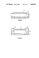
FIG. 2 through FIG. 8 schematically illustrate main steps of a method to fabricate an image sensor according to the present invention.
FIG. 9 through FIG. 13 schematically illustrate main steps of a second method to fabricate an image sensor according to the present invention.
Referring to FIGS. 1(a) through (c), a structure of an image sensor according to the present invention is hereinafter explained. The general structure is that an array of picture cells for image sensing are located along the center line b-b'. CCDs 13 for transferring and outputting the signal charges produced in picture cells are symmetrically arranged at both sides of the line b-b', further more, main peripheral portions, such as 2-phase buses 16-1' and 16-2' to charge-transfer electrodes 8 of the CCD 13, are symmetrically arranged outside of the charge transfer electrodes 8.
On a p- -type semiconductor substrate 1, an n-type region 5 is doped to form a p-n junction with the substrate. A photo gate 7 is formed in a SiO2 insulation layer 17 by a silicon gate technique to hold the picture cells at a predetermined potential. A light injected through an opening 15' of an aluminum coating 11, through a PSG (phospho silicate glass) passivation film 10 and through a window 15 of an SiO2 layer film 18 into the p-n junction, produces signal charges in the p-n junction depending on the intensity of the injected light. A picture cell 19 of the image sensor is thus constituted there, as well known. Each picture cell 19 is isolated from each other by a field isolation 3 shown by the hatched area in FIGS. 1(a) and (c). As for its thickness, explanation shall be given later in detail. Underneath the field isolation 3, a p+ -type region 6' is formed as a channel stop to prevent a lateral conduction path between the adjacent cells through the substrate 1, as well known. The signal charge produced by the injected light in the n-type region 5 of the picture cell is transferred by a transfer gate 9 into under a corresponding one of the charge transfer electrodes 8 of the CCD 13. Underneath each of the charge transfer electrodes 8, an n-type region 4 is formed for storing and transferring the signal charges. Arrays of the charge transfer electrodes 8 of polycrystalline silicon together with the n-type region 4 are thus forming the CCD 13, as well known. In a peripheral portion of the CCD, a pair of the electrodes 8, one shown by solid lines and one shown by dotted lines, is connected together alternatively to a patterned aluminum bus 16-1', and the next pair to 16-2', each formed on an insulation layer 2 of SiO2, as well known. These two groups of patterned buses are supplied with 2-phase clock pulses φ1 and φ2 respectively for the charge transfer operation. The CCD portion is illustrated merely schematically in FIGS. 1 omitting the details.
The supplied voltage to the CCD portion is generally as high as 12 V inherently required for charge transfer operation. The insulation layer 2 is approximately 8000Åthick, enough to prevent the field effect of the voltage, 12 V, of the aluminum buses 16-1', 16-2' and polycrystalline silicon lead 16-1, 16-2 onto the region 6 which must be inactive underneath the insulation layer 2. The transfer gate 9 is also supplied with 12 V. Where the transfer gate 9 must exert its influence (i.e. field effect) on the substrate for its charge transfer operation, the transfer gate 9 is located close to the substrate 1. However, at a portion where the transfer gate 9 must not exert its influence on the substrate, the transfer gate 9 is separated from the substrate 1 by the thick insulation layer 2' which is fabricated together with the insulation layer 2 and has the same thickness, as shown in FIG. 1(b).
Thickness of the field isolation 3 is approximately 3000 to 4000Å, which is less than that of the insulation layer 2. The width is approximately 2 μm or less, which can be achieved due to its reduced thickness, because the width laterally inflates wider when the thickness is inflated by the thermal oxidization. The applied voltage on the picture cells as well as the photo gate 7 is generally 5 V. Thus, the field isolation can be narrowed as long as the field isolation 3 can isolate the neighboring picture cells. The narrowed width of the field isolation contribures to provide an adequate area for each picture cell, which means fair sensitivity of light detection, as well as fair opening ratio of the picture cells, as high as approximately 70%. The opening ratio is essential for obtaining more accurate information of the light intensity. Accurate information means information from a wider area of the picture cell.
Two fabrication methods of the image sensor according to the present invention are hereinafter described.
A first method is explained, referring to FIG. 2 through FIG. 8, schematically illustrating only main steps and a main portion related to embody the method of the present invention. The steps are:
(1) On a portion where a field isolation 24 (i.e. 2 of FIG. 1, and cited as the first insulation layer in the claims) of the peripheral portion is to be fabricated on a p- -type semiconductor substrate 1, a p+ -type impurity 22' is doped for preparing a channel stop, by a known method, such as ion implantation. An SiO2 layer 23 is formed over the substrate 21, so as to cover all the surface including the doped regions 22' as thick as approximately 1000 Å, by a known method, such as thermal oxidization. The order of these processes can be reversed.
(2) A silicon nitride (referred to hereinafter as Si3 N4) film 25 is formed over the the SiO2 film 22, so as to cover the area except for the area for fabricating an insulation layer in the peripheral portion of the CCD as shown in FIG. 2 using known methods, such as CVD (chemical vapor deposition) and a photo lithography technique. The Si3 N4 film 25 can be commonly used as a mask of the above-mentioned ion implantation.
(3) Approximately 7000Åthick SiO2 layers 24 are formed on the exposed portion, i.e. not-masked portion by the Si3 N4 film 25, of the SiO2 layer 23 by a known method, such as selective oxidization method, i.e. so called LOCOS (Local Oxidization of Silicon) as shown in FIG. 3. Silicon inflates both vertically and laterally when it is oxidized, thus the surface becomes taller and the p+ region 22' is moved down deeper into the substrate. Thus, the field isolation 24 and its channel stop 22 are fabricated.
(4) A photo resist film 26 is formed all over the Si3 N4 film 25 as well as over the inflated insulation layer 24, as shown in FIG. 4.
(5) An opening 24A is formed in the photo resist film 26, on a portion where a picture cell is fabricated, by a known method, such as lithography technique. Exposed portion of the Si3 N4 film 25 through the opening of the photo resist film is etched by a known method, such as a wet etching method, so that the opening 24A is made to expose the SiO2 layer 23 therein, as shown in FIG. 5.
(6) A p+ -type dopant 27', such as boron, is doped into the p- -type substrate 21 through the SiO2 layer 23 by a known method, such as ion implantation, for preparing a channel stop, as shown in FIG. 6.
(7) The photo resist film 26 is removed by a known method such as a stripping process. Then, the exposed portion of SiO2 layer 23 through the opening 24A is additionally oxidized by a known method, such as thermal oxidization, so that the SiO2 in the opening 24A is inflated to be as thick as 3000 to 4000Å. Thus the field isolation 28, which is cited as the second insulation layer in the claims, is fabricated between the picture cells as shown in FIG. 7. Then, the p+ -type dopant 27' forms a channel stop region 27 underneath the fabricated field isolation 28.
(8) The Si3 N4 film 25 used as an etching mask is removed, as shown in FIG. 8.
A second method is explained, referring to FIG. 9 through FIG. 13, schematically illustrating only the main steps and the main portion related to the embodiment of the method of the present invention. The steps of the method are:
(1) On a portion where an insulation layer 24 (i.e. 2 of FIGS. 1) of the peripheral portion of the CCD as well as a portion where field isolation 28 (i.e. 3 of FIGS. 1) for picture cells is to be fabricated on a p- -type semiconductor substrate 21, p+ -type impurity 22' and 27' are selectively doped to prepare channel stops, by a known method, such as ion implantation. An SiO2 layer 23' is formed on the substrate 21, so as to cover all the surface including the doped regions 22' and 27' as thick as approximately 1000 Å, by a known method, such as thermal oxidization. The order of these processes can be reversed.
(2) A Si3 N4 film 29 is formed over the the SiO2 layer 23', so as to cover the area except for an area for fabricating an insulation layer 24 for the peripheral portion of the CCD as well as an area for a field isolation 28 of the picture cell using a known method, such as CVD and photo lithography technique, as shown in FIG. 9. The Si3 N4 film 29 can be commonly used as a mask for the above-mentioned ion implantation.
(3) Approximately 3000 to 4000Åthick SiO2 layers 24' and 28 are formed on the exposed portions, i.e. not masked portion by the Si3 N4 film 29, of the SiO2 layer 23 by a known, method, such as selective thermal oxidization method, i.e. so called LOCOS, as shown in FIG. 10, in similar manner to those of FIG. 3. Thus, the field isolation 28 is fabricated.
(4) A Si3 N4 film 31 is formed to cover the field isolation 28 by known methods, such as CVD and photo lithography technique, as shown in FIG. 11.
(5) The exposed SiO2 layer 24' is further oxidized, using the Si3 N4 film 29 and 31 as masks, by employing a known method, such as thermal oxidization method, until the exposed SiO2 layer 24' is inflated as thick as approximately 8000Å, thus the insulation layer 24 is fabricated.
(6) The Si3 N4 film 29 and 31 used as masks are removed by a known method as a stripping process. Thus insulation layers 24 and 28 of different thickness are formed as shown in FIG. 13.
Successive steps, such as forming silicon gates 7, 8, 8', 9, 16-1 and 16-2 and so on, following the step (8) of the first method or the step (6) of the second method are the same as those of the prior art, therefore no more description or drawing are given hereinafter. An insulation layer 2' on which the transfer gate 9 having 12 V is formed is omitted in the explanation referring to FIG. 2 through FIG. 9, because the insulation layer 24 can representatively explain the invention in simplified drawings.
The insulation layer 24 (i.e. 2 of FIGS. 1), fabricated by the above-described methods is thick enough to withstand the applied voltage 12 V, while the field isolation 28, (i.e. 3 of FIGS. 1) is thin and narrow enough to withstand the applied voltage 5 V. Thus, the width of the field isolation 3 can achieve less than a half of that of the prior art, resulting in a fair opening ratio, which is a ratio of the opened width of the picture cell to the cell pitch, achieving more than 70%, compared with about 50% if the prior art is applied thereto. The fair value of the opening ratio means accurate light information received by each picture cell. Consequently, according to the present invention, 5K-pixel image sensor with 2K-pixel size outputting accurate light information is achieved causing no malfunction due to poor isolation of the cells nor difficulty of production.
The many features and advantages of the invention are apparent from the detailed specification and thus, it is intended by the appended claims to cover all such features and advantages of the system which fall within the true spirit and scope of the invention. Further, since numerous modifications and changes will readily occur to those skilled in the art, it is not desired to limit the invention to the exact construction and operation shown and described, and accordingly, all suitable modifications and equivalents may be resorted to, falling within the scope of the invention.
Claims (3)
1. An image sensor formed on a semiconductor substrate, comprising:
a plurality of semiconductor light detection cells formed on said semiconductor substrate, each of said light detection cells producing electrical signal charges responding to intensity of a light projected thereon;
a charge - coupled device formed on said semiconductor substrate, operatively connected to said light detection cells for transferring and outputting electrical signal charges produced in said light detection cells;
a first field insulation layer formed on said semiconductor substrate, for isolating a patterned wiring of a peripheral portion of said charge-coupled device from said semiconductor substrate; and
a second field insulation layer formed in said semiconductor substrate which selectively extends into a surface of semiconductor substrate, for demarcating an area forming each of said light detecting cells, as well as of isolating and electrically insulating adjacent ones of said light detection cells, a thickness of said second field insulation layer being essentially thinner than a thickness of said first field insulation layer.
2. An image sensor according to claim 1, wherein the thickness of said first field insulation layer is adequate to withstand an applied voltage to said patterned wiring of the peripheral portion, as well as the thickness of said second field insulation layer is adequate to withstand an applied voltage to said light detection cells.
3. An image sensor formed on a semiconductor substrate having a first conductivity type, comprising:
a plurality of semiconductor light detection cells, each formed on a region having a second conductivity type opposite said first conductivity type in said semiconductor substrate, for producing electrical signal charges responding to intensity of a light projected thereon;
a charge-coupled device formed on said semiconductor substrate, connected to said light detection cells, for transferring and outputting electrical signal charges produced in said light detection cells;
a first field insulation layer formed on said semiconductor substrate, for isolating a patterned wiring of a peripheral portion of said charge-coupled device from said semiconductor substrate; and
a second field insulation layer formed on said semiconductor substrate to selectivley extend into a surface of said semiconductor substrate, for demarcating said region of the second conductivity type forming each of said light detection cells, as well s for isolating and electrically insulating adjacent ones of said light detection cells, a thickness of said second field insulation layer being essentially thinner than a thickness of said first field insulation layer.
Applications Claiming Priority (2)
| Application Number | Priority Date | Filing Date | Title |
|---|---|---|---|
| JP61-119347 | 1986-05-26 | ||
| JP61119347A JPS63153A (en) | 1986-05-26 | 1986-05-26 | Charge transfer device |
Related Parent Applications (1)
| Application Number | Title | Priority Date | Filing Date |
|---|---|---|---|
| US07049920 Continuation | 1987-05-15 |
Publications (1)
| Publication Number | Publication Date |
|---|---|
| US4910568A true US4910568A (en) | 1990-03-20 |
Family
ID=14759238
Family Applications (1)
| Application Number | Title | Priority Date | Filing Date |
|---|---|---|---|
| US07/346,268 Expired - Fee Related US4910568A (en) | 1986-05-26 | 1989-05-01 | Image sensor |
Country Status (5)
| Country | Link |
|---|---|
| US (1) | US4910568A (en) |
| EP (1) | EP0247942B1 (en) |
| JP (1) | JPS63153A (en) |
| KR (1) | KR900008650B1 (en) |
| DE (1) | DE3788978T2 (en) |
Cited By (23)
| Publication number | Priority date | Publication date | Assignee | Title |
|---|---|---|---|---|
| US5122649A (en) * | 1989-12-11 | 1992-06-16 | Fuji Photo Film Co., Ltd. | Solid-state imaging device having a predetermined impurity layer embedded between two adjacent sets of switching transistors |
| US5166511A (en) * | 1989-05-08 | 1992-11-24 | Interuniversitair Micro-Elektronica Centrum Vzw | Radiaton-sensitive sensor having a plurality of radiation sensitive elements arranged substantially circular with radially decreasing density |
| US5243215A (en) * | 1990-05-31 | 1993-09-07 | Fuji Electric Co., Ltd. | Semiconductor photodiode device with reduced junction area |
| US5385849A (en) * | 1993-05-17 | 1995-01-31 | Nec Corporation | Process of fabricating solid-state image pick-up device free from crystal defects in active region |
| US5504355A (en) * | 1991-12-10 | 1996-04-02 | Nec Corporation | Solid state image sensor device having two layer wiring structure |
| US20100302427A1 (en) * | 2009-06-01 | 2010-12-02 | Shen Wang | Ccd image sensors having multiple lateral overflow drain regions for a horizontal shift register |
| US20110220971A1 (en) * | 2009-09-17 | 2011-09-15 | Sionyx, Inc. | Photosensitive imaging devices and associated methods |
| US20160197109A1 (en) * | 2008-04-09 | 2016-07-07 | Sony Corporation | Solid-state imaging device, production method thereof, and electronic device |
| US9496308B2 (en) | 2011-06-09 | 2016-11-15 | Sionyx, Llc | Process module for increasing the response of backside illuminated photosensitive imagers and associated methods |
| US9673243B2 (en) | 2009-09-17 | 2017-06-06 | Sionyx, Llc | Photosensitive imaging devices and associated methods |
| US9673250B2 (en) | 2013-06-29 | 2017-06-06 | Sionyx, Llc | Shallow trench textured regions and associated methods |
| US9741761B2 (en) | 2010-04-21 | 2017-08-22 | Sionyx, Llc | Photosensitive imaging devices and associated methods |
| US9739046B2 (en) | 2014-03-12 | 2017-08-22 | Joseph S. Miskovich | Modular stormwater retention and management system |
| US9761739B2 (en) | 2010-06-18 | 2017-09-12 | Sionyx, Llc | High speed photosensitive devices and associated methods |
| US9762830B2 (en) | 2013-02-15 | 2017-09-12 | Sionyx, Llc | High dynamic range CMOS image sensor having anti-blooming properties and associated methods |
| US9905599B2 (en) | 2012-03-22 | 2018-02-27 | Sionyx, Llc | Pixel isolation elements, devices and associated methods |
| US9911781B2 (en) | 2009-09-17 | 2018-03-06 | Sionyx, Llc | Photosensitive imaging devices and associated methods |
| US9939251B2 (en) | 2013-03-15 | 2018-04-10 | Sionyx, Llc | Three dimensional imaging utilizing stacked imager devices and associated methods |
| USD840498S1 (en) | 2017-08-09 | 2019-02-12 | J.M. Sales Associates, Inc. | Modular fluid retention and management tray |
| US10244188B2 (en) | 2011-07-13 | 2019-03-26 | Sionyx, Llc | Biometric imaging devices and associated methods |
| US10361083B2 (en) | 2004-09-24 | 2019-07-23 | President And Fellows Of Harvard College | Femtosecond laser-induced formation of submicrometer spikes on a semiconductor substrate |
| US10374109B2 (en) | 2001-05-25 | 2019-08-06 | President And Fellows Of Harvard College | Silicon-based visible and near-infrared optoelectric devices |
| US10597861B2 (en) | 2014-03-12 | 2020-03-24 | J.M. Sales Associates, Inc. | Modular stormwater retention system |
Citations (6)
| Publication number | Priority date | Publication date | Assignee | Title |
|---|---|---|---|---|
| JPS5588374A (en) * | 1978-12-27 | 1980-07-04 | Fujitsu Ltd | Charge transferring device |
| US4378565A (en) * | 1980-10-01 | 1983-03-29 | General Electric Company | Integrated circuit and method of making same |
| US4484210A (en) * | 1980-09-05 | 1984-11-20 | Nippon Electric Co., Ltd. | Solid-state imaging device having a reduced image lag |
| US4618874A (en) * | 1983-09-07 | 1986-10-21 | Kabushiki Kaisha Toshiba | Solid state imaging device |
| US4658278A (en) * | 1985-04-15 | 1987-04-14 | Rca Corporation | High density charge-coupled device imager and method of making the same |
| US4675982A (en) * | 1985-10-31 | 1987-06-30 | International Business Machines Corporation | Method of making self-aligned recessed oxide isolation regions |
Family Cites Families (1)
| Publication number | Priority date | Publication date | Assignee | Title |
|---|---|---|---|---|
| JPS598350A (en) * | 1982-07-06 | 1984-01-17 | Nec Corp | Semiconductor integrated circuit device |
-
1986
- 1986-05-26 JP JP61119347A patent/JPS63153A/en active Pending
-
1987
- 1987-05-21 KR KR1019870005053A patent/KR900008650B1/en not_active IP Right Cessation
- 1987-05-26 EP EP87401187A patent/EP0247942B1/en not_active Expired - Lifetime
- 1987-05-26 DE DE3788978T patent/DE3788978T2/en not_active Expired - Fee Related
-
1989
- 1989-05-01 US US07/346,268 patent/US4910568A/en not_active Expired - Fee Related
Patent Citations (6)
| Publication number | Priority date | Publication date | Assignee | Title |
|---|---|---|---|---|
| JPS5588374A (en) * | 1978-12-27 | 1980-07-04 | Fujitsu Ltd | Charge transferring device |
| US4484210A (en) * | 1980-09-05 | 1984-11-20 | Nippon Electric Co., Ltd. | Solid-state imaging device having a reduced image lag |
| US4378565A (en) * | 1980-10-01 | 1983-03-29 | General Electric Company | Integrated circuit and method of making same |
| US4618874A (en) * | 1983-09-07 | 1986-10-21 | Kabushiki Kaisha Toshiba | Solid state imaging device |
| US4658278A (en) * | 1985-04-15 | 1987-04-14 | Rca Corporation | High density charge-coupled device imager and method of making the same |
| US4675982A (en) * | 1985-10-31 | 1987-06-30 | International Business Machines Corporation | Method of making self-aligned recessed oxide isolation regions |
Cited By (37)
| Publication number | Priority date | Publication date | Assignee | Title |
|---|---|---|---|---|
| US5166511A (en) * | 1989-05-08 | 1992-11-24 | Interuniversitair Micro-Elektronica Centrum Vzw | Radiaton-sensitive sensor having a plurality of radiation sensitive elements arranged substantially circular with radially decreasing density |
| US5122649A (en) * | 1989-12-11 | 1992-06-16 | Fuji Photo Film Co., Ltd. | Solid-state imaging device having a predetermined impurity layer embedded between two adjacent sets of switching transistors |
| US5243215A (en) * | 1990-05-31 | 1993-09-07 | Fuji Electric Co., Ltd. | Semiconductor photodiode device with reduced junction area |
| US5504355A (en) * | 1991-12-10 | 1996-04-02 | Nec Corporation | Solid state image sensor device having two layer wiring structure |
| US5385849A (en) * | 1993-05-17 | 1995-01-31 | Nec Corporation | Process of fabricating solid-state image pick-up device free from crystal defects in active region |
| US10374109B2 (en) | 2001-05-25 | 2019-08-06 | President And Fellows Of Harvard College | Silicon-based visible and near-infrared optoelectric devices |
| US10741399B2 (en) | 2004-09-24 | 2020-08-11 | President And Fellows Of Harvard College | Femtosecond laser-induced formation of submicrometer spikes on a semiconductor substrate |
| US10361083B2 (en) | 2004-09-24 | 2019-07-23 | President And Fellows Of Harvard College | Femtosecond laser-induced formation of submicrometer spikes on a semiconductor substrate |
| US20160197109A1 (en) * | 2008-04-09 | 2016-07-07 | Sony Corporation | Solid-state imaging device, production method thereof, and electronic device |
| US10438983B2 (en) * | 2008-04-09 | 2019-10-08 | Sony Corporation | Solid-state imaging device, production method thereof, and electronic device |
| US20100302427A1 (en) * | 2009-06-01 | 2010-12-02 | Shen Wang | Ccd image sensors having multiple lateral overflow drain regions for a horizontal shift register |
| US8605187B2 (en) * | 2009-06-01 | 2013-12-10 | Truesense Imaging, Inc. | CCD image sensors having multiple lateral overflow drain regions for a horizontal shift register |
| US9911781B2 (en) | 2009-09-17 | 2018-03-06 | Sionyx, Llc | Photosensitive imaging devices and associated methods |
| US9673243B2 (en) | 2009-09-17 | 2017-06-06 | Sionyx, Llc | Photosensitive imaging devices and associated methods |
| US20110220971A1 (en) * | 2009-09-17 | 2011-09-15 | Sionyx, Inc. | Photosensitive imaging devices and associated methods |
| US10361232B2 (en) | 2009-09-17 | 2019-07-23 | Sionyx, Llc | Photosensitive imaging devices and associated methods |
| US8476681B2 (en) * | 2009-09-17 | 2013-07-02 | Sionyx, Inc. | Photosensitive imaging devices and associated methods |
| US10229951B2 (en) | 2010-04-21 | 2019-03-12 | Sionyx, Llc | Photosensitive imaging devices and associated methods |
| US9741761B2 (en) | 2010-04-21 | 2017-08-22 | Sionyx, Llc | Photosensitive imaging devices and associated methods |
| US10505054B2 (en) | 2010-06-18 | 2019-12-10 | Sionyx, Llc | High speed photosensitive devices and associated methods |
| US9761739B2 (en) | 2010-06-18 | 2017-09-12 | Sionyx, Llc | High speed photosensitive devices and associated methods |
| US10269861B2 (en) | 2011-06-09 | 2019-04-23 | Sionyx, Llc | Process module for increasing the response of backside illuminated photosensitive imagers and associated methods |
| US9496308B2 (en) | 2011-06-09 | 2016-11-15 | Sionyx, Llc | Process module for increasing the response of backside illuminated photosensitive imagers and associated methods |
| US9666636B2 (en) | 2011-06-09 | 2017-05-30 | Sionyx, Llc | Process module for increasing the response of backside illuminated photosensitive imagers and associated methods |
| US10244188B2 (en) | 2011-07-13 | 2019-03-26 | Sionyx, Llc | Biometric imaging devices and associated methods |
| US10224359B2 (en) | 2012-03-22 | 2019-03-05 | Sionyx, Llc | Pixel isolation elements, devices and associated methods |
| US9905599B2 (en) | 2012-03-22 | 2018-02-27 | Sionyx, Llc | Pixel isolation elements, devices and associated methods |
| US9762830B2 (en) | 2013-02-15 | 2017-09-12 | Sionyx, Llc | High dynamic range CMOS image sensor having anti-blooming properties and associated methods |
| US9939251B2 (en) | 2013-03-15 | 2018-04-10 | Sionyx, Llc | Three dimensional imaging utilizing stacked imager devices and associated methods |
| US10347682B2 (en) | 2013-06-29 | 2019-07-09 | Sionyx, Llc | Shallow trench textured regions and associated methods |
| US9673250B2 (en) | 2013-06-29 | 2017-06-06 | Sionyx, Llc | Shallow trench textured regions and associated methods |
| US11069737B2 (en) | 2013-06-29 | 2021-07-20 | Sionyx, Llc | Shallow trench textured regions and associated methods |
| US9739046B2 (en) | 2014-03-12 | 2017-08-22 | Joseph S. Miskovich | Modular stormwater retention and management system |
| US10597861B2 (en) | 2014-03-12 | 2020-03-24 | J.M. Sales Associates, Inc. | Modular stormwater retention system |
| USD840498S1 (en) | 2017-08-09 | 2019-02-12 | J.M. Sales Associates, Inc. | Modular fluid retention and management tray |
| USD868934S1 (en) | 2017-08-09 | 2019-12-03 | J.M. Sales Associates, Inc. | Modular fluid retention and management tray |
| USD868935S1 (en) | 2017-08-09 | 2019-12-03 | J.M. Sales Associates, Inc. | Modular fluid retention and management tray |
Also Published As
| Publication number | Publication date |
|---|---|
| DE3788978T2 (en) | 1994-05-19 |
| JPS63153A (en) | 1988-01-05 |
| KR870011699A (en) | 1987-12-26 |
| EP0247942A3 (en) | 1990-09-26 |
| KR900008650B1 (en) | 1990-11-26 |
| EP0247942B1 (en) | 1994-02-02 |
| EP0247942A2 (en) | 1987-12-02 |
| DE3788978D1 (en) | 1994-03-17 |
Similar Documents
| Publication | Publication Date | Title |
|---|---|---|
| US4910568A (en) | Image sensor | |
| US4844776A (en) | Method for making folded extended window field effect transistor | |
| US5731237A (en) | Method of producing an EPROM with a trench insulating layer | |
| US4922311A (en) | Folded extended window field effect transistor | |
| US6482692B2 (en) | Method of manufacturing a semiconductor device, having first and second semiconductor regions with field shield isolation structures and a field oxide film covering a junction between semiconductor regions | |
| US4055885A (en) | Charge transfer semiconductor device with electrodes separated by oxide region therebetween and method for fabricating the same | |
| US4686759A (en) | Method of manufacturing a semiconductor device | |
| JP3003590B2 (en) | Solid-state imaging device and method of manufacturing the same | |
| US6335220B1 (en) | Solid state imaging device with four-phase charge-coupled device and method of manufacturing the same | |
| US20030132367A1 (en) | Solid state image pickup device with polysilicon transfer electrodes | |
| KR100233315B1 (en) | Semiconductor integrated circuit and a method of manufacturing the same | |
| US6482667B2 (en) | Solid state image sensor device and method of fabricating the same | |
| US4677737A (en) | Self aligned zero overlap charge coupled device | |
| US6987294B2 (en) | Charge-coupled device and method of fabricating the same | |
| US4133099A (en) | Method of manufacturing a charge transfer device | |
| JP2830215B2 (en) | Method for manufacturing charge transfer device | |
| JP2910394B2 (en) | Solid-state imaging device and method of manufacturing the same | |
| JPH06296008A (en) | Manufacture of solid-state image pickup element | |
| JPH10125873A (en) | Semiconductor integrated circuit device and manufacture for forming arch type gate field effect transistor(fet) on main surface of semiconductor substrate | |
| JP2562609B2 (en) | Method for manufacturing semiconductor device | |
| JP2910369B2 (en) | Manufacturing method of floating gate type semiconductor memory device | |
| KR100261999B1 (en) | Method for fabricating gate flash cell | |
| JPH04207077A (en) | Manufacture of solid-state image pickup element | |
| JPH09246500A (en) | Semiconductor storage device and manufacture | |
| JPH0917985A (en) | Image pickup element and manufacturing method thereof |
Legal Events
| Date | Code | Title | Description |
|---|---|---|---|
| FEPP | Fee payment procedure |
Free format text: PAYOR NUMBER ASSIGNED (ORIGINAL EVENT CODE: ASPN); ENTITY STATUS OF PATENT OWNER: LARGE ENTITY |
|
| REMI | Maintenance fee reminder mailed | ||
| LAPS | Lapse for failure to pay maintenance fees | ||
| FP | Lapsed due to failure to pay maintenance fee |
Effective date: 19980325 |
|
| STCH | Information on status: patent discontinuation |
Free format text: PATENT EXPIRED DUE TO NONPAYMENT OF MAINTENANCE FEES UNDER 37 CFR 1.362 |