US4964134A - Semiconductor laser structures - Google Patents
Semiconductor laser structures Download PDFInfo
- Publication number
- US4964134A US4964134A US07/254,934 US25493488A US4964134A US 4964134 A US4964134 A US 4964134A US 25493488 A US25493488 A US 25493488A US 4964134 A US4964134 A US 4964134A
- Authority
- US
- United States
- Prior art keywords
- laser structure
- active material
- structure according
- laser
- doped
- Prior art date
- Legal status (The legal status is an assumption and is not a legal conclusion. Google has not performed a legal analysis and makes no representation as to the accuracy of the status listed.)
- Expired - Lifetime
Links
Images


Classifications
-
- H—ELECTRICITY
- H01—ELECTRIC ELEMENTS
- H01L—SEMICONDUCTOR DEVICES NOT COVERED BY CLASS H10
- H01L33/00—Semiconductor devices with at least one potential-jump barrier or surface barrier specially adapted for light emission; Processes or apparatus specially adapted for the manufacture or treatment thereof or of parts thereof; Details thereof
- H01L33/02—Semiconductor devices with at least one potential-jump barrier or surface barrier specially adapted for light emission; Processes or apparatus specially adapted for the manufacture or treatment thereof or of parts thereof; Details thereof characterised by the semiconductor bodies
- H01L33/04—Semiconductor devices with at least one potential-jump barrier or surface barrier specially adapted for light emission; Processes or apparatus specially adapted for the manufacture or treatment thereof or of parts thereof; Details thereof characterised by the semiconductor bodies with a quantum effect structure or superlattice, e.g. tunnel junction
- H01L33/06—Semiconductor devices with at least one potential-jump barrier or surface barrier specially adapted for light emission; Processes or apparatus specially adapted for the manufacture or treatment thereof or of parts thereof; Details thereof characterised by the semiconductor bodies with a quantum effect structure or superlattice, e.g. tunnel junction within the light emitting region, e.g. quantum confinement structure or tunnel barrier
-
- B—PERFORMING OPERATIONS; TRANSPORTING
- B82—NANOTECHNOLOGY
- B82Y—SPECIFIC USES OR APPLICATIONS OF NANOSTRUCTURES; MEASUREMENT OR ANALYSIS OF NANOSTRUCTURES; MANUFACTURE OR TREATMENT OF NANOSTRUCTURES
- B82Y20/00—Nanooptics, e.g. quantum optics or photonic crystals
-
- H—ELECTRICITY
- H01—ELECTRIC ELEMENTS
- H01S—DEVICES USING THE PROCESS OF LIGHT AMPLIFICATION BY STIMULATED EMISSION OF RADIATION [LASER] TO AMPLIFY OR GENERATE LIGHT; DEVICES USING STIMULATED EMISSION OF ELECTROMAGNETIC RADIATION IN WAVE RANGES OTHER THAN OPTICAL
- H01S5/00—Semiconductor lasers
- H01S5/10—Construction or shape of the optical resonator, e.g. extended or external cavity, coupled cavities, bent-guide, varying width, thickness or composition of the active region
- H01S5/11—Comprising a photonic bandgap structure
-
- H—ELECTRICITY
- H01—ELECTRIC ELEMENTS
- H01S—DEVICES USING THE PROCESS OF LIGHT AMPLIFICATION BY STIMULATED EMISSION OF RADIATION [LASER] TO AMPLIFY OR GENERATE LIGHT; DEVICES USING STIMULATED EMISSION OF ELECTROMAGNETIC RADIATION IN WAVE RANGES OTHER THAN OPTICAL
- H01S5/00—Semiconductor lasers
- H01S5/10—Construction or shape of the optical resonator, e.g. extended or external cavity, coupled cavities, bent-guide, varying width, thickness or composition of the active region
- H01S5/12—Construction or shape of the optical resonator, e.g. extended or external cavity, coupled cavities, bent-guide, varying width, thickness or composition of the active region the resonator having a periodic structure, e.g. in distributed feedback [DFB] lasers
- H01S5/1231—Grating growth or overgrowth details
-
- H—ELECTRICITY
- H01—ELECTRIC ELEMENTS
- H01S—DEVICES USING THE PROCESS OF LIGHT AMPLIFICATION BY STIMULATED EMISSION OF RADIATION [LASER] TO AMPLIFY OR GENERATE LIGHT; DEVICES USING STIMULATED EMISSION OF ELECTROMAGNETIC RADIATION IN WAVE RANGES OTHER THAN OPTICAL
- H01S5/00—Semiconductor lasers
- H01S5/30—Structure or shape of the active region; Materials used for the active region
- H01S5/305—Structure or shape of the active region; Materials used for the active region characterised by the doping materials used in the laser structure
-
- H—ELECTRICITY
- H01—ELECTRIC ELEMENTS
- H01S—DEVICES USING THE PROCESS OF LIGHT AMPLIFICATION BY STIMULATED EMISSION OF RADIATION [LASER] TO AMPLIFY OR GENERATE LIGHT; DEVICES USING STIMULATED EMISSION OF ELECTROMAGNETIC RADIATION IN WAVE RANGES OTHER THAN OPTICAL
- H01S5/00—Semiconductor lasers
- H01S5/30—Structure or shape of the active region; Materials used for the active region
- H01S5/34—Structure or shape of the active region; Materials used for the active region comprising quantum well or superlattice structures, e.g. single quantum well [SQW] lasers, multiple quantum well [MQW] lasers or graded index separate confinement heterostructure [GRINSCH] lasers
-
- H—ELECTRICITY
- H01—ELECTRIC ELEMENTS
- H01S—DEVICES USING THE PROCESS OF LIGHT AMPLIFICATION BY STIMULATED EMISSION OF RADIATION [LASER] TO AMPLIFY OR GENERATE LIGHT; DEVICES USING STIMULATED EMISSION OF ELECTROMAGNETIC RADIATION IN WAVE RANGES OTHER THAN OPTICAL
- H01S5/00—Semiconductor lasers
- H01S5/06—Arrangements for controlling the laser output parameters, e.g. by operating on the active medium
- H01S5/0618—Details on the linewidth enhancement parameter alpha
-
- H—ELECTRICITY
- H01—ELECTRIC ELEMENTS
- H01S—DEVICES USING THE PROCESS OF LIGHT AMPLIFICATION BY STIMULATED EMISSION OF RADIATION [LASER] TO AMPLIFY OR GENERATE LIGHT; DEVICES USING STIMULATED EMISSION OF ELECTROMAGNETIC RADIATION IN WAVE RANGES OTHER THAN OPTICAL
- H01S5/00—Semiconductor lasers
- H01S5/20—Structure or shape of the semiconductor body to guide the optical wave ; Confining structures perpendicular to the optical axis, e.g. index or gain guiding, stripe geometry, broad area lasers, gain tailoring, transverse or lateral reflectors, special cladding structures, MQW barrier reflection layers
- H01S5/22—Structure or shape of the semiconductor body to guide the optical wave ; Confining structures perpendicular to the optical axis, e.g. index or gain guiding, stripe geometry, broad area lasers, gain tailoring, transverse or lateral reflectors, special cladding structures, MQW barrier reflection layers having a ridge or stripe structure
- H01S5/223—Buried stripe structure
-
- H—ELECTRICITY
- H01—ELECTRIC ELEMENTS
- H01S—DEVICES USING THE PROCESS OF LIGHT AMPLIFICATION BY STIMULATED EMISSION OF RADIATION [LASER] TO AMPLIFY OR GENERATE LIGHT; DEVICES USING STIMULATED EMISSION OF ELECTROMAGNETIC RADIATION IN WAVE RANGES OTHER THAN OPTICAL
- H01S5/00—Semiconductor lasers
- H01S5/30—Structure or shape of the active region; Materials used for the active region
- H01S5/305—Structure or shape of the active region; Materials used for the active region characterised by the doping materials used in the laser structure
- H01S5/3054—Structure or shape of the active region; Materials used for the active region characterised by the doping materials used in the laser structure p-doping
-
- H—ELECTRICITY
- H01—ELECTRIC ELEMENTS
- H01S—DEVICES USING THE PROCESS OF LIGHT AMPLIFICATION BY STIMULATED EMISSION OF RADIATION [LASER] TO AMPLIFY OR GENERATE LIGHT; DEVICES USING STIMULATED EMISSION OF ELECTROMAGNETIC RADIATION IN WAVE RANGES OTHER THAN OPTICAL
- H01S5/00—Semiconductor lasers
- H01S5/30—Structure or shape of the active region; Materials used for the active region
- H01S5/32—Structure or shape of the active region; Materials used for the active region comprising PN junctions, e.g. hetero- or double- heterostructures
- H01S5/3202—Structure or shape of the active region; Materials used for the active region comprising PN junctions, e.g. hetero- or double- heterostructures grown on specifically orientated substrates, or using orientation dependent growth
-
- H—ELECTRICITY
- H01—ELECTRIC ELEMENTS
- H01S—DEVICES USING THE PROCESS OF LIGHT AMPLIFICATION BY STIMULATED EMISSION OF RADIATION [LASER] TO AMPLIFY OR GENERATE LIGHT; DEVICES USING STIMULATED EMISSION OF ELECTROMAGNETIC RADIATION IN WAVE RANGES OTHER THAN OPTICAL
- H01S5/00—Semiconductor lasers
- H01S5/30—Structure or shape of the active region; Materials used for the active region
- H01S5/34—Structure or shape of the active region; Materials used for the active region comprising quantum well or superlattice structures, e.g. single quantum well [SQW] lasers, multiple quantum well [MQW] lasers or graded index separate confinement heterostructure [GRINSCH] lasers
- H01S5/3428—Structure or shape of the active region; Materials used for the active region comprising quantum well or superlattice structures, e.g. single quantum well [SQW] lasers, multiple quantum well [MQW] lasers or graded index separate confinement heterostructure [GRINSCH] lasers layer orientation perpendicular to the substrate
-
- H—ELECTRICITY
- H01—ELECTRIC ELEMENTS
- H01S—DEVICES USING THE PROCESS OF LIGHT AMPLIFICATION BY STIMULATED EMISSION OF RADIATION [LASER] TO AMPLIFY OR GENERATE LIGHT; DEVICES USING STIMULATED EMISSION OF ELECTROMAGNETIC RADIATION IN WAVE RANGES OTHER THAN OPTICAL
- H01S5/00—Semiconductor lasers
- H01S5/30—Structure or shape of the active region; Materials used for the active region
- H01S5/34—Structure or shape of the active region; Materials used for the active region comprising quantum well or superlattice structures, e.g. single quantum well [SQW] lasers, multiple quantum well [MQW] lasers or graded index separate confinement heterostructure [GRINSCH] lasers
- H01S5/343—Structure or shape of the active region; Materials used for the active region comprising quantum well or superlattice structures, e.g. single quantum well [SQW] lasers, multiple quantum well [MQW] lasers or graded index separate confinement heterostructure [GRINSCH] lasers in AIIIBV compounds, e.g. AlGaAs-laser, InP-based laser
- H01S5/34306—Structure or shape of the active region; Materials used for the active region comprising quantum well or superlattice structures, e.g. single quantum well [SQW] lasers, multiple quantum well [MQW] lasers or graded index separate confinement heterostructure [GRINSCH] lasers in AIIIBV compounds, e.g. AlGaAs-laser, InP-based laser emitting light at a wavelength longer than 1000nm, e.g. InP based 1300 and 1500nm lasers
-
- H—ELECTRICITY
- H01—ELECTRIC ELEMENTS
- H01S—DEVICES USING THE PROCESS OF LIGHT AMPLIFICATION BY STIMULATED EMISSION OF RADIATION [LASER] TO AMPLIFY OR GENERATE LIGHT; DEVICES USING STIMULATED EMISSION OF ELECTROMAGNETIC RADIATION IN WAVE RANGES OTHER THAN OPTICAL
- H01S5/00—Semiconductor lasers
- H01S5/30—Structure or shape of the active region; Materials used for the active region
- H01S5/34—Structure or shape of the active region; Materials used for the active region comprising quantum well or superlattice structures, e.g. single quantum well [SQW] lasers, multiple quantum well [MQW] lasers or graded index separate confinement heterostructure [GRINSCH] lasers
- H01S5/343—Structure or shape of the active region; Materials used for the active region comprising quantum well or superlattice structures, e.g. single quantum well [SQW] lasers, multiple quantum well [MQW] lasers or graded index separate confinement heterostructure [GRINSCH] lasers in AIIIBV compounds, e.g. AlGaAs-laser, InP-based laser
- H01S5/34313—Structure or shape of the active region; Materials used for the active region comprising quantum well or superlattice structures, e.g. single quantum well [SQW] lasers, multiple quantum well [MQW] lasers or graded index separate confinement heterostructure [GRINSCH] lasers in AIIIBV compounds, e.g. AlGaAs-laser, InP-based laser with a well layer having only As as V-compound, e.g. AlGaAs, InGaAs
Definitions
- the present invention relates to semiconductor laser structures and finds application in optical communications.
- the radiation used in optical communications is not necessarily strictly in the visible region. If silica optical fibres are used as the transmission medium, infra-red radiation is of special usefulness since the loss minima occur in such fibres at 1.3 ⁇ m and 1.55 ⁇ m approximately. (The above wavelengths are in vacuo wavelengths as are all wavelengths herein except where otherwise specifically stated).
- a semiconductor laser structure will include a p-n junction across which a driving current can be applied (the conventional current from p to n), an "active region" in which electrons and holes combine, producing photons by stimulated emission, and a feedback structure to cause oscillation of radiation in the active region.
- the active region has to relate suitably in band gap and refractive index to the other semiconductor regions of the structure in order to achieve a suitable degree of "confinement" of these processes to the active region.
- Semiconductor lasers comprising regions of gallium arsenide and gallium aluminium arsenide are also used for communications purposes. They operate near to 0.9 ⁇ m.
- the feedback structure might comprise for instance reflective end facets of the laser (Fabry-Perot or FP lasers). Alternatively it might comprise a grating of corrugations which lie near the active region (distributed feedback or DFB lasers). The corrugations may be shifted to a position external to the laser structure, adjacent the emission axis (a distributed Bragg reflector or DBR laser), or a reflective interface may be used in a cavity external to the laser.
- a distributed feedback or DFB laser distributed feedback
- a double heterostructure (DH) laser may comprise an (initially undoped) active region of a first material, lying between a lower n-doped layer and an upper p-doped layer each of a different material.
- the active region comprises one or more very thin layers of active material, and where a plurality of such layers are provided, they are separated by barrier layers.
- the thin active layers are each so thin that that dimension is comparable to the De Broglie wavelength for electrons, and the discreteness of the density distribution of energy states in the active material becomes apparent.
- Quantum well layers have thicknesses (known as well width) typically of the order of 10 nm and the barrier layers may be still thinner.
- Semiconductor laser structures are used in devices other than optical sources. For instance, if the driving current applied is less than a lasing threshold driving current, a laser structure may still be useful as an optical amplifier, amplifying an optical radiation input signal. Further, a laser structure may be used as an absorption modulator, a device coupled to a laser output port which can be switched between optically opaque and transparent conditions with respect to the laser output and so modulate it.
- Laser structures vary considerably from each other in a number of operating characteristics.
- transient wavelength chirping is a phenomenon which occurs for instance either when a laser is switched on and off to produce a directly modulated output signal, or when an absorption modulator is used. It has the effect of distorting the oscillation frequency of an optical pulse, the pulse then tending to spread during transmission in a dispersive medium and causing difficulty in detection.
- coherent optical communications it is important that the continuous wave emitted radiation shows a narrow linewidth. This allows coherent detection systems, such as heterodyne or homodyne detection, to be used which are more sensitive than direct detection and give better bandwidth discrimination.
- Unmodified FP lasers have been found unsuitable, having linewidths of more than 100 MHz. It is known that DBR and DFB lasers can be fabricated having narrower emission linewidths and that external structures such as external cavities can result in narrowed emission linewidths. However, both emission linewidth and transient wavelength chirping have tended to remain unpredictable characteristics in the design of laser structures.
- a direct band gap semiconductor laser structure whose emission wavelength is less than its active material band-gap equivalent wavelength by an amount such that the emitted photon energy is equal or approximately equal to the sum of the band gap energy and the conduction band quasi Fermi level measured from the conduction band edge, the active material of the laser structure being doped p-type to a level at which the laser structure shows positive gain under working conditions.
- the present invention comprises a direct band gap semi-conductor laser structure having means for determining its emission wavelength, wherein the following relationships are satisfied: ##EQU1## where E is the emitted photon energy
- Eg is the band gap energy
- Efc is the conduction band quasi Fermi level measured from the conduction band edge
- Efv is the valence band quasi Fermi level measured from the valence band edge
- the dopant used in doping the active material of the laser structure p-type should not be a dopant which reduces the radiative efficiency of the material to a degree rendering it unacceptable opaque under the woking conditions, particularly the emission wavelength selected, of the laser structure.
- Zn although a widely used p-type dopant is unlikely to be suitable but Be (berillium) is likely to be suitable.
- the value of (E-Eg) should be as close as possible to the value of (Mc/Mr) Efc.
- Mc, Mr and Mv have been measured for a wide variety of semiconductor materials and their values published. They can for instance be determined by reference to the book "Physics of Semiconductor Devices” by S M Sze, published by Wiley Interscience.
- Eg in the case of a bulk semiconductor laser structure that is a laser structure which does not include a quantum well active layer
- Eg is the effective band gap energy between the lowermost energy state of the conduction band and the highest energy of the valence band, and can be assessed in terms of the well width, for instance in accordance with the relationship quoted by M Asada, A Kaneyama and Y Suematsu in the IEEE Journal of Quantum Electronics, OE20, July 1984.
- Efc in a bulk semiconductor laser structure can be taken to be
- N is the injected carrier density (which can be determined from the carrier lifetime in the material concerned, and the driving current used)
- Nc is the conduction band effective density of states (published and determinable as for Mc, Mr and Mv above)
- T is the absolute temperature
- Efc in a QW laser structure can be taken to be
- n Dirac's constant
- L z is the well width
- Efv in a bulk semiconductor laser structure can be taken to be
- P is the hole density of the active layer material and equals the sum of the injected carrier density N and the level of p-doping Na (in a p-doped material), and
- Nv is the valence band effective density of states in the active layer material (published and determinable as for Mc, Mr and Mv above)
- Efv in a QW laser structure can be taken to be
- Nv a typical value of Nv for a semiconductor laser material is 1.2 ⁇ 10 19 cm -3 .
- the material of the active layer would then have to be doped p-type to a level Na at least of the order of 8 ⁇ 10 18 cm -3 , for instance 7.8 ⁇ 10 18 cm -3 or above.
- the use of a bulk semiconductor laser structure can have an advantage in optical communications in that materials used to produce the active layer will emit radiation at the wavelength 1.55 ⁇ m particularly easily. This is advantageous as mentioned above, for use with silica optical fibres.
- the valence band is degenerate when ##EQU3##
- ##EQU4## equals about 4.7 ⁇ 10 16 m -2 .
- P must be of the order of at least 4.7 ⁇ 10 18 cm -3 . That is, half the hole density necessary for a bulk semiconductor laser structure.
- the material of the active layer would only have to be doped p-type to a level Na at least of the order of 4 ⁇ 10 18 cm -3 , for instance 3.8 ⁇ 10 18 cm -3 or above.
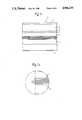
- FIGS. 1a and 1b show a cross section of the laser structure
- FIG. 2 shows a graph of the linewidth enhancement factor ⁇ plotted as a function of photon energy, for three different QW laser structures with undoped active material
- FIG. 3 shows a graph of ⁇ plotted as a function of photon energy at three different injected carrier densities for the active material of the laser structure of FIG. 1;
- FIG. 4 shows the relationship between gain, the injected carrier density N, the p-doping level Na, and the conduction band quasi Fermi level Efc for the laser structure of FIG. 1;
- FIGS. 5a and 5b show the relationship between gain, N, Na and Efc for a bulk semiconductor structure
- FIG. 6 shows schematically a cross section of an alternative laser structure to that of FIGS. 1a and 1b.
- the laser structure 1 is a DFB laser structure having an internal grating 2. Parallel to the plane of the grating 2 extend five quantum well active layers 3. Overall, the structure is planar, comprising fourteen different layers 3 to 9 grown epitaxially onto a substrate 10.
- the laser structure 1 comprises the following:
- a substrate 10 of InP approximately 100 ⁇ m thick, with a surface corresponding to the (100) crystal plane. It is doped n-type with Sn to a level in the range from 1 to 6, ⁇ 10 18 cm -3 .
- cladding/buffer layer 4 of InP 1.0 ⁇ m thick, doped n-type with Sn to a level in the range from 1 to 6, ⁇ 10 18 cm -3 ;
- a multiple quantum well layer stack comprising five active layers 3 of In 0 .53 Ga 0 .47 As, each 10 nm thick, separated by four barriers 5 of InP, each 5 nm thick.
- Each layer 3 and barrier 5 of the stack is doped p-type with Be to a level of 4.3 ⁇ 10 18 cm -3 .
- cladding layer 6 of InP 0.1 ⁇ m thick, doped p-type with Be to a level in the range 1 to 5, ⁇ 10 18 cm -3 ;
- a cladding layer 8 of InP 1.0 ⁇ m thick, doped p-type with Be to a level in the range 1 to 5, ⁇ 10 18 cm -3 ;
- the exposed face of the substrate 10 is metallised with a Sn/Au alloy in the proportions 2:98 and the exposed face of the contact layer 9 is metallised with a Ti/Au bilayer, these metallisations being known, for the purpose of supplying a driving current to the laser structure 1.
- the grating 2 comprises corrugations which extend in the (110) crystal direction on the uppermost surface of the waveguiding layer 7.
- the period of the corrugations is 0.44 ⁇ m, and they comprise triangular cross section grooves, approximately 0.15 ⁇ m deep.
- All the layers of the laser structure can be grown by known molecular beam epitaxial (MBE) techniques.
- MBE molecular beam epitaxial
- the grating can be produced by chemical etching through an electron-beam-exposed mask in the manner described by Westbrook et al, Electronics Letters 1982 18 pages 863 to 865.
- Berillium is used to dope the active layers 3 because it shows a relatively low degree of non-radiative recombination in use. Because of the high doping level Na, such recombination can be relatively significant with certain other dopants, such as zinc.
- the thickness of the active layers 3, 10 nm is selected to achieve a particular effective bandgap equivalent wavelength of 1.55 ⁇ m, and hence a particular value of Eg, for instance in accordance with the relationship quoted by M Asada, A Kameyama and Y Suematsu in the IEEE Journal of Quantum Electronics, OE 20, July 1984.
- the laser structure 1 will start to emit radiation of wavelength 1.44 ⁇ m, determined in accordance with the Bragg condition for reflection by the period of the grating 2, when a driving current at least equal to the lasing threshold current is applied.
- Efv is approximately equal to -kTlog e (exp ⁇ n 2 PLz/kTMv-1) for a quantum well laser in which ##EQU6##
- the multiple quantum well laser structure described above could be incorporated into any of a number of forms of lateral confinement laser structures, such as ridge waveguide or buried heterostructure.
- L is the device length
- x m is the "mirror" loss of the structure, determined by facet reflectivity in a Fabry-Perot laser and by grating strength in a DFB laser.
- Vg is the group velocity
- p(e) is the density of states which equals ##EQU10##
- the laser structure 1 described above is a multiple QW structure, it is not necessary that such a structure be used.
- a bulk semiconductor structure might be used instead.
- the valence band quasi Fermi level is given by ##EQU14##
- laser structures of other types might be used instead.
- the laser structures described above comprise particular materials containing In, Ga, As and P, other combinations of these elements, or even other material systems, may well be found suitable, for instance to achieve different values of Eg and different emitted photon energies.
- ⁇ will be required to have a value of less than or equal to 2, more preferably less than or equal to 1, and more preferably of less than or equal to 0.5.
- T L Koch and J E Bowers in Electronics Letters, December 1984, pp 1038 to 1040 a small radio frequency signal is used to amplitude modulate the output of a laser. Any frequency modulation present is detected. Where no frequency modulation is present, ⁇ has the value 0.
Abstract
Description
=kT(log(N/Nc)+0.35(N/Nc))
=kT log(exp(πn.sup.2 NL.sub.z /kTMc)-1)
=-kT(log(P/Nv)+0.35(P/Nv))
=-kT log(exp(πn.sup.2 PL.sub.z /kTMv)-1).
Efc=log(expπn.sup.2 NLz/kTMc-1)
Claims (11)
1/Mr=1/Mc+1/Mv
Applications Claiming Priority (2)
| Application Number | Priority Date | Filing Date | Title |
|---|---|---|---|
| GB8703743 | 1987-02-18 | ||
| GB878703743A GB8703743D0 (en) | 1987-02-18 | 1987-02-18 | Semiconductor laser structures |
Publications (1)
| Publication Number | Publication Date |
|---|---|
| US4964134A true US4964134A (en) | 1990-10-16 |
Family
ID=10612496
Family Applications (1)
| Application Number | Title | Priority Date | Filing Date |
|---|---|---|---|
| US07/254,934 Expired - Lifetime US4964134A (en) | 1987-02-18 | 1988-02-18 | Semiconductor laser structures |
Country Status (9)
| Country | Link |
|---|---|
| US (1) | US4964134A (en) |
| EP (1) | EP0279680B1 (en) |
| JP (1) | JPH01503024A (en) |
| AT (1) | ATE97518T1 (en) |
| CA (1) | CA1295722C (en) |
| DE (1) | DE3885627T2 (en) |
| ES (1) | ES2047028T3 (en) |
| GB (1) | GB8703743D0 (en) |
| WO (1) | WO1988006360A1 (en) |
Cited By (26)
| Publication number | Priority date | Publication date | Assignee | Title |
|---|---|---|---|---|
| US5107514A (en) * | 1990-04-13 | 1992-04-21 | Mitsubishi Denki Kabushiki Kaisha | Semiconductor optical element |
| WO1992017801A2 (en) * | 1991-03-27 | 1992-10-15 | Massachusetts Institute Of Technology | Solid state optical converter |
| US5255278A (en) * | 1991-07-10 | 1993-10-19 | Nec Corporation | Semiconductor laser with vertical resonator |
| US5291328A (en) * | 1989-01-13 | 1994-03-01 | British Telecommunications | Semiconductor laser amplifiers |
| US5305403A (en) * | 1989-12-07 | 1994-04-19 | British Telecommunications Public Limited Company | Optical waveguide and method of making an optical waveguide |
| US5440581A (en) * | 1992-01-13 | 1995-08-08 | Canon Kabushiki Kaisha | Semiconductor optical filter and an optical communication system using the same |
| US6108360A (en) * | 1997-06-06 | 2000-08-22 | Razeghi; Manijeh | Long wavelength DH, SCH and MQW lasers based on Sb |
| US6384961B2 (en) | 1999-05-24 | 2002-05-07 | Molecular Optoelectronics Corporation | Compact optical amplifier with integrated optical waveguide and pump source |
| US6511571B2 (en) | 1998-07-23 | 2003-01-28 | Molecular Optoelectronics Corporation | Method for fabricating an optical waveguide |
| US6628691B2 (en) * | 2000-11-22 | 2003-09-30 | Fujitsu Limited | Laser diode |
| US20100279446A1 (en) * | 2005-03-07 | 2010-11-04 | Joseph Reid Henrichs | Optical phase conjugation laser diode |
| US20130001729A1 (en) * | 2008-03-06 | 2013-01-03 | Sionyx, Inc. | High Fill-Factor Laser-Treated Semiconductor Device on Bulk Material with Single Side Contact Scheme |
| US20130308178A1 (en) * | 2012-05-17 | 2013-11-21 | Finisar Corporation | Co-modulation of DBR Laser and Integrated Optical Amplifier |
| US9496308B2 (en) | 2011-06-09 | 2016-11-15 | Sionyx, Llc | Process module for increasing the response of backside illuminated photosensitive imagers and associated methods |
| US9673243B2 (en) | 2009-09-17 | 2017-06-06 | Sionyx, Llc | Photosensitive imaging devices and associated methods |
| US9673250B2 (en) | 2013-06-29 | 2017-06-06 | Sionyx, Llc | Shallow trench textured regions and associated methods |
| US9741761B2 (en) | 2010-04-21 | 2017-08-22 | Sionyx, Llc | Photosensitive imaging devices and associated methods |
| US9762830B2 (en) | 2013-02-15 | 2017-09-12 | Sionyx, Llc | High dynamic range CMOS image sensor having anti-blooming properties and associated methods |
| US9761739B2 (en) | 2010-06-18 | 2017-09-12 | Sionyx, Llc | High speed photosensitive devices and associated methods |
| US9905599B2 (en) | 2012-03-22 | 2018-02-27 | Sionyx, Llc | Pixel isolation elements, devices and associated methods |
| US9911781B2 (en) | 2009-09-17 | 2018-03-06 | Sionyx, Llc | Photosensitive imaging devices and associated methods |
| US9939251B2 (en) | 2013-03-15 | 2018-04-10 | Sionyx, Llc | Three dimensional imaging utilizing stacked imager devices and associated methods |
| US10244188B2 (en) | 2011-07-13 | 2019-03-26 | Sionyx, Llc | Biometric imaging devices and associated methods |
| US10361083B2 (en) | 2004-09-24 | 2019-07-23 | President And Fellows Of Harvard College | Femtosecond laser-induced formation of submicrometer spikes on a semiconductor substrate |
| US10374109B2 (en) | 2001-05-25 | 2019-08-06 | President And Fellows Of Harvard College | Silicon-based visible and near-infrared optoelectric devices |
| US11424596B2 (en) * | 2018-06-25 | 2022-08-23 | Otto-Von-Guericke-Universitaet Magdeburg | Semiconductor layer stack and method for producing same |
Citations (1)
| Publication number | Priority date | Publication date | Assignee | Title |
|---|---|---|---|---|
| US4257011A (en) * | 1977-08-01 | 1981-03-17 | Hitachi, Ltd. | Semiconductor laser device |
-
1987
- 1987-02-18 GB GB878703743A patent/GB8703743D0/en active Pending
-
1988
- 1988-02-18 AT AT88301395T patent/ATE97518T1/en not_active IP Right Cessation
- 1988-02-18 CA CA000559253A patent/CA1295722C/en not_active Expired - Lifetime
- 1988-02-18 JP JP63501940A patent/JPH01503024A/en active Pending
- 1988-02-18 EP EP88301395A patent/EP0279680B1/en not_active Expired - Lifetime
- 1988-02-18 DE DE3885627T patent/DE3885627T2/en not_active Expired - Lifetime
- 1988-02-18 ES ES88301395T patent/ES2047028T3/en not_active Expired - Lifetime
- 1988-02-18 WO PCT/GB1988/000101 patent/WO1988006360A1/en unknown
- 1988-02-18 US US07/254,934 patent/US4964134A/en not_active Expired - Lifetime
Patent Citations (1)
| Publication number | Priority date | Publication date | Assignee | Title |
|---|---|---|---|---|
| US4257011A (en) * | 1977-08-01 | 1981-03-17 | Hitachi, Ltd. | Semiconductor laser device |
Non-Patent Citations (26)
| Title |
|---|
| Applied Physics Letters, vol. 42, No. 8, 15 Apr. 1983, American Institute of Physics, (New York US), K. Vahala et al.: "On the Linewidth Enhancement Factor α in Semiconductor Injection Lasers", pp. 631-633. |
| Applied Physics Letters, vol. 42, No. 8, 15 Apr. 1983, American Institute of Physics, (New York US), K. Vahala et al.: On the Linewidth Enhancement Factor in Semiconductor Injection Lasers , pp. 631 633. * |
| Arakawa, Y,; Vahala, K.; Yariv, A., Applied Physics Letter vol. 45, p. 950, 1984. * |
| Arakawa, Y.; Yariv, A., IEEE J. Quantum Electronics, QE 22, p. 1887, 1986. * |
| Arakawa, Y.; Yariv, A., IEEE J. Quantum Electronics, QE-22, p. 1887, 1986. |
| Asada, M.; Kaneyama, A.; Suematsu, Y; IEEE J. Quantum Electronics, QE 20, Jul. 1984. * |
| Asada, M.; Kaneyama, A.; Suematsu, Y;-IEEE J. Quantum Electronics, QE-20, Jul. 1984. |
| Electronics Letters, vol. 19, No. 22, 27 Oct. 1983, (Hitchin, Herts, GB), I. D. Henning et al.: "Measurements of the Semiconductor Laser Linewidth Broadening Factor", pp. 927-929. |
| Electronics Letters, vol. 19, No. 22, 27 Oct. 1983, (Hitchin, Herts, GB), I. D. Henning et al.: Measurements of the Semiconductor Laser Linewidth Broadening Factor , pp. 927 929. * |
| Electronics Letters, vol. 19, No. 6, 17 Mar. 1983, (Hitchin, Herts, GB), M. G. Burt: "Gain Spectra of Quantum-Well Lasers", pp. 210-211. |
| Electronics Letters, vol. 19, No. 6, 17 Mar. 1983, (Hitchin, Herts, GB), M. G. Burt: Gain Spectra of Quantum Well Lasers , pp. 210 211. * |
| Electronics Letters, vol. 20, No. 1, 5 Jan. 1984, (London, GB) M. G. Burt: "Linewidth Enhancement Factor for Quantum-Well Lasers", pp. 27-29. |
| Electronics Letters, vol. 20, No. 1, 5 Jan. 1984, (London, GB) M. G. Burt: Linewidth Enhancement Factor for Quantum Well Lasers , pp. 27 29. * |
| Electronics Letters, vol. 21, No. 13, 20 Jun. 1985, (Stevenage, Hertz, GB), N. K. Dutta et al.: "Fabrication and Performance Characteristics of InGaAsP Ridge-Guide Distributed-Feedback Multi-Quantum-Well Lasers", pp. 571-573. |
| Electronics Letters, vol. 21, No. 13, 20 Jun. 1985, (Stevenage, Hertz, GB), N. K. Dutta et al.: Fabrication and Performance Characteristics of InGaAsP Ridge Guide Distributed Feedback Multi Quantum Well Lasers , pp. 571 573. * |
| Green, C. A., Dutta, N. K.; Watson. W., Applied Physics Letters, vol. 50, No. 20, pp. 1409 1410, 1987. * |
| Green, C. A., Dutta, N. K.; Watson. W., Applied Physics Letters, vol. 50, No. 20, pp. 1409-1410, 1987. |
| Henry, C. H.; IEEE J. Quantum Electronics, QE 18(2), Feb. 1982, pp. 259 264. * |
| Henry, C. H.; IEEE J. Quantum Electronics, QE-18(2), Feb. 1982, pp. 259-264. |
| IEEE Journal of Quantum Electronics, vol. QE 21, No. 10, Oct. 1985, (IEEE, New York, US), Y. Arakawa et al.: Theory of Gain, Modulation Reseponse, and Spectral Linewidth in AlGaAs Quantum Well Lasers , pp. 1666 1674. * |
| IEEE Journal of Quantum Electronics, vol. QE-21, No. 10, Oct. 1985, (IEEE, New York, US), Y. Arakawa et al.: "Theory of Gain, Modulation Reseponse, and Spectral Linewidth in AlGaAs Quantum Well Lasers", pp. 1666-1674. |
| Japanese Journal of Applied Physics, vol. 24, No. 7, part 2, Jul. 1985, (Tokyo, JP), N. Ogasawara et al.: "Linewidth Enhancement Factor in GaAS/AlGaAs Multi-Quantum-Well Lasers", pp, L519-L521. |
| Japanese Journal of Applied Physics, vol. 24, No. 7, part 2, Jul. 1985, (Tokyo, JP), N. Ogasawara et al.: Linewidth Enhancement Factor in GaAS/AlGaAs Multi Quantum Well Lasers , pp, L519 L521. * |
| Uomi, K.; Ohtoshi, T.; and Chinone N., Japan Journal Applied Physics, 24 L539, 1985. * |
| Uomi, K.; Ohtoshi, T.; and Chinone, N.; "Ultra High Relaxation Oscillation Frequency (-50 GHz) in Modulation Doped Multiquantum Well (MD-MQW) Lasers: Theoretical Analysis", Central Research Laboratory, Hitachi, Ltd., Kokubunji, Tokyo, 185, pp. 184-185. |
| Uomi, K.; Ohtoshi, T.; and Chinone, N.; Ultra High Relaxation Oscillation Frequency ( 50 GHz) in Modulation Doped Multiquantum Well (MD MQW) Lasers: Theoretical Analysis , Central Research Laboratory, Hitachi, Ltd., Kokubunji, Tokyo, 185, pp. 184 185. * |
Cited By (41)
| Publication number | Priority date | Publication date | Assignee | Title |
|---|---|---|---|---|
| US5291328A (en) * | 1989-01-13 | 1994-03-01 | British Telecommunications | Semiconductor laser amplifiers |
| US5305403A (en) * | 1989-12-07 | 1994-04-19 | British Telecommunications Public Limited Company | Optical waveguide and method of making an optical waveguide |
| US5107514A (en) * | 1990-04-13 | 1992-04-21 | Mitsubishi Denki Kabushiki Kaisha | Semiconductor optical element |
| WO1992017801A2 (en) * | 1991-03-27 | 1992-10-15 | Massachusetts Institute Of Technology | Solid state optical converter |
| WO1992017801A3 (en) * | 1991-03-27 | 1992-11-26 | Massachusetts Inst Technology | Solid state optical converter |
| US5313324A (en) * | 1991-03-27 | 1994-05-17 | Massachusetts Institute Of Technology | Solid state optical converter |
| US5255278A (en) * | 1991-07-10 | 1993-10-19 | Nec Corporation | Semiconductor laser with vertical resonator |
| US5440581A (en) * | 1992-01-13 | 1995-08-08 | Canon Kabushiki Kaisha | Semiconductor optical filter and an optical communication system using the same |
| US6108360A (en) * | 1997-06-06 | 2000-08-22 | Razeghi; Manijeh | Long wavelength DH, SCH and MQW lasers based on Sb |
| US6511571B2 (en) | 1998-07-23 | 2003-01-28 | Molecular Optoelectronics Corporation | Method for fabricating an optical waveguide |
| US6384961B2 (en) | 1999-05-24 | 2002-05-07 | Molecular Optoelectronics Corporation | Compact optical amplifier with integrated optical waveguide and pump source |
| US6628691B2 (en) * | 2000-11-22 | 2003-09-30 | Fujitsu Limited | Laser diode |
| US10374109B2 (en) | 2001-05-25 | 2019-08-06 | President And Fellows Of Harvard College | Silicon-based visible and near-infrared optoelectric devices |
| US10741399B2 (en) | 2004-09-24 | 2020-08-11 | President And Fellows Of Harvard College | Femtosecond laser-induced formation of submicrometer spikes on a semiconductor substrate |
| US10361083B2 (en) | 2004-09-24 | 2019-07-23 | President And Fellows Of Harvard College | Femtosecond laser-induced formation of submicrometer spikes on a semiconductor substrate |
| US20100279446A1 (en) * | 2005-03-07 | 2010-11-04 | Joseph Reid Henrichs | Optical phase conjugation laser diode |
| US20130001729A1 (en) * | 2008-03-06 | 2013-01-03 | Sionyx, Inc. | High Fill-Factor Laser-Treated Semiconductor Device on Bulk Material with Single Side Contact Scheme |
| US10361232B2 (en) | 2009-09-17 | 2019-07-23 | Sionyx, Llc | Photosensitive imaging devices and associated methods |
| US9673243B2 (en) | 2009-09-17 | 2017-06-06 | Sionyx, Llc | Photosensitive imaging devices and associated methods |
| US9911781B2 (en) | 2009-09-17 | 2018-03-06 | Sionyx, Llc | Photosensitive imaging devices and associated methods |
| US9741761B2 (en) | 2010-04-21 | 2017-08-22 | Sionyx, Llc | Photosensitive imaging devices and associated methods |
| US10229951B2 (en) | 2010-04-21 | 2019-03-12 | Sionyx, Llc | Photosensitive imaging devices and associated methods |
| US9761739B2 (en) | 2010-06-18 | 2017-09-12 | Sionyx, Llc | High speed photosensitive devices and associated methods |
| US10505054B2 (en) | 2010-06-18 | 2019-12-10 | Sionyx, Llc | High speed photosensitive devices and associated methods |
| US9496308B2 (en) | 2011-06-09 | 2016-11-15 | Sionyx, Llc | Process module for increasing the response of backside illuminated photosensitive imagers and associated methods |
| US9666636B2 (en) | 2011-06-09 | 2017-05-30 | Sionyx, Llc | Process module for increasing the response of backside illuminated photosensitive imagers and associated methods |
| US10269861B2 (en) | 2011-06-09 | 2019-04-23 | Sionyx, Llc | Process module for increasing the response of backside illuminated photosensitive imagers and associated methods |
| US10244188B2 (en) | 2011-07-13 | 2019-03-26 | Sionyx, Llc | Biometric imaging devices and associated methods |
| US9905599B2 (en) | 2012-03-22 | 2018-02-27 | Sionyx, Llc | Pixel isolation elements, devices and associated methods |
| US10224359B2 (en) | 2012-03-22 | 2019-03-05 | Sionyx, Llc | Pixel isolation elements, devices and associated methods |
| US20130308178A1 (en) * | 2012-05-17 | 2013-11-21 | Finisar Corporation | Co-modulation of DBR Laser and Integrated Optical Amplifier |
| US9231367B2 (en) * | 2012-05-17 | 2016-01-05 | Finisar Corporation | Co-modulation of DBR laser and integrated optical amplifier |
| US9831631B2 (en) | 2012-05-17 | 2017-11-28 | Finisar Corporation | Directly modulated laser for PON application |
| US9762830B2 (en) | 2013-02-15 | 2017-09-12 | Sionyx, Llc | High dynamic range CMOS image sensor having anti-blooming properties and associated methods |
| US9939251B2 (en) | 2013-03-15 | 2018-04-10 | Sionyx, Llc | Three dimensional imaging utilizing stacked imager devices and associated methods |
| US10347682B2 (en) | 2013-06-29 | 2019-07-09 | Sionyx, Llc | Shallow trench textured regions and associated methods |
| US9673250B2 (en) | 2013-06-29 | 2017-06-06 | Sionyx, Llc | Shallow trench textured regions and associated methods |
| US11069737B2 (en) | 2013-06-29 | 2021-07-20 | Sionyx, Llc | Shallow trench textured regions and associated methods |
| US11424596B2 (en) * | 2018-06-25 | 2022-08-23 | Otto-Von-Guericke-Universitaet Magdeburg | Semiconductor layer stack and method for producing same |
| US20220368110A1 (en) * | 2018-06-25 | 2022-11-17 | Otto-Von-Guericke-Universitaet Magdeburg | Semiconductor layer stack and method for producing same |
| US11870220B2 (en) * | 2018-06-25 | 2024-01-09 | Otto-Von-Guericke-Universitaet Magdeburg | Semiconductor layer stack and method for producing same |
Also Published As
| Publication number | Publication date |
|---|---|
| GB8703743D0 (en) | 1987-03-25 |
| EP0279680A1 (en) | 1988-08-24 |
| JPH01503024A (en) | 1989-10-12 |
| ES2047028T3 (en) | 1994-02-16 |
| DE3885627D1 (en) | 1993-12-23 |
| CA1295722C (en) | 1992-02-11 |
| EP0279680B1 (en) | 1993-11-18 |
| WO1988006360A1 (en) | 1988-08-25 |
| DE3885627T2 (en) | 1994-05-19 |
| ATE97518T1 (en) | 1993-12-15 |
Similar Documents
| Publication | Publication Date | Title |
|---|---|---|
| US4964134A (en) | Semiconductor laser structures | |
| US5252839A (en) | Superluminescent light-emitting diode with reverse biased absorber | |
| EP0218344B1 (en) | Semiconductor lasers | |
| EP0400559B1 (en) | Semiconductor optical device | |
| Utaka et al. | Lasing characteristics of 1.5-1.6 µm GaInAsP/InP integrated twin-guide lasers with first-order distributed Bragg reflectors | |
| EP0759217A1 (en) | Strain-compensated multiple quantum well laser structures | |
| Sugimura | Auger recombination effect on threshold current of InGaAsP quantum well lasers | |
| Oomura et al. | Low threshold InGaAsP/InP buried crescent laser with double current confinement structure | |
| US4831630A (en) | Phased-locked window lasers | |
| Song et al. | High-power broad-band superluminescent diode with low spectral modulation at 1.5-μm wavelength | |
| Dutta et al. | Strain compensated InGaAs-GaAsP-InGaP laser | |
| Dutta et al. | Gain and carrier lifetime measurements in AlGaAs single quantum well lasers | |
| US6879612B1 (en) | Temperature insensitive VCSEL | |
| EP0512681B1 (en) | Semiconductor laser diode | |
| US5737353A (en) | Multiquantum-well semiconductor laser | |
| Schanen et al. | Fabrication and lasing characteristics of λ= 1.56 μm tunable twin-guide (TTG) DFB lasers | |
| EP0549123B1 (en) | Semiconductor laser having reduced temperature dependence | |
| US7072373B2 (en) | Ridge waveguide semiconductor laser diode | |
| Ishikawa et al. | Well-thickness dependence of high-temperature characteristics in 1.3-μm AlGaInAs-InP strained-multiple-quantum-well lasers | |
| US5329134A (en) | Superluminescent diode having a quantum well and cavity length dependent threshold current | |
| Yasaka et al. | Pure effects of strain in strained-layer multiple-quantum-well lasers | |
| Yano et al. | Temperature characteristics of double-carrier-confinement (DCC) heterojunction InGaAsP (λ= 1.3 µm)/InP lasers | |
| Noda et al. | Ridge waveguide AlGaAs/GaAs distributed feedback lasers with multiple quantum well structure | |
| US7084444B2 (en) | Method and apparatus for improving efficiency in opto-electronic radiation source devices | |
| US20050078724A1 (en) | Single mode distributed feedback lasers |
Legal Events
| Date | Code | Title | Description |
|---|---|---|---|
| AS | Assignment |
Owner name: BRITISH TELECOMMUNICATIONS PUBLIC LIMITED COMPANY, Free format text: ASSIGNMENT OF ASSIGNORS INTEREST.;ASSIGNORS:WESTBROOK, LESLIE D.;ADAMS, MICHAEL J.;REEL/FRAME:004963/0508 Effective date: 19880928 Owner name: BRITISH TELECOMMUNICATIONS PUBLIC LIMITED COMPANY, Free format text: ASSIGNMENT OF ASSIGNORS INTEREST;ASSIGNORS:WESTBROOK, LESLIE D.;ADAMS, MICHAEL J.;REEL/FRAME:004963/0508 Effective date: 19880928 |
|
| STCF | Information on status: patent grant |
Free format text: PATENTED CASE |
|
| FEPP | Fee payment procedure |
Free format text: PAYOR NUMBER ASSIGNED (ORIGINAL EVENT CODE: ASPN); ENTITY STATUS OF PATENT OWNER: LARGE ENTITY |
|
| FPAY | Fee payment |
Year of fee payment: 4 |
|
| FPAY | Fee payment |
Year of fee payment: 8 |
|
| FPAY | Fee payment |
Year of fee payment: 12 |
|
| AS | Assignment |
Owner name: IPG PHOTONICS CORPORATION, MASSACHUSETTS Free format text: ASSIGNMENT OF ASSIGNORS INTEREST;ASSIGNOR:BRITISH TELECOMMUNICATIONS PLC;REEL/FRAME:020582/0143 Effective date: 20080221 |