US5017804A - Hall sensing of bond wire current - Google Patents
Hall sensing of bond wire current Download PDFInfo
- Publication number
- US5017804A US5017804A US07/340,445 US34044589A US5017804A US 5017804 A US5017804 A US 5017804A US 34044589 A US34044589 A US 34044589A US 5017804 A US5017804 A US 5017804A
- Authority
- US
- United States
- Prior art keywords
- current
- conductor
- hall effect
- effect sensors
- semiconductor
- Prior art date
- Legal status (The legal status is an assumption and is not a legal conclusion. Google has not performed a legal analysis and makes no representation as to the accuracy of the status listed.)
- Expired - Lifetime
Links
Images


Classifications
-
- H—ELECTRICITY
- H03—ELECTRONIC CIRCUITRY
- H03K—PULSE TECHNIQUE
- H03K17/00—Electronic switching or gating, i.e. not by contact-making and –breaking
- H03K17/51—Electronic switching or gating, i.e. not by contact-making and –breaking characterised by the components used
- H03K17/90—Electronic switching or gating, i.e. not by contact-making and –breaking characterised by the components used by the use, as active elements, of galvano-magnetic devices, e.g. Hall-effect devices
-
- G—PHYSICS
- G01—MEASURING; TESTING
- G01R—MEASURING ELECTRIC VARIABLES; MEASURING MAGNETIC VARIABLES
- G01R15/00—Details of measuring arrangements of the types provided for in groups G01R17/00 - G01R29/00, G01R33/00 - G01R33/26 or G01R35/00
- G01R15/14—Adaptations providing voltage or current isolation, e.g. for high-voltage or high-current networks
- G01R15/20—Adaptations providing voltage or current isolation, e.g. for high-voltage or high-current networks using galvano-magnetic devices, e.g. Hall-effect devices, i.e. measuring a magnetic field via the interaction between a current and a magnetic field, e.g. magneto resistive or Hall effect devices
- G01R15/202—Adaptations providing voltage or current isolation, e.g. for high-voltage or high-current networks using galvano-magnetic devices, e.g. Hall-effect devices, i.e. measuring a magnetic field via the interaction between a current and a magnetic field, e.g. magneto resistive or Hall effect devices using Hall-effect devices
Definitions
- This invention pertains to sensing current through a bonding wire, or similar type of conductor, in close proximity to Hall effect devices.
- FIG. 1 shows a typical prior art load circuit wherein a switching device, in this example an MOS field effect transistor (MOSFET) 10, is controlled by an input signal applied to terminal 14 for selectively applying a voltage source VCC available on drain 13 of MOSFET 10 to output terminal 12 connected to source 15 of MOSFET 10.
- a switching device in this example an MOS field effect transistor (MOSFET) 10
- MOSFET MOS field effect transistor
- an external terminal 12 is available for connection to load device 11, which has its other terminal connected to ground.
- power supply VCC is selectively connected to load device 11.
- FIG. 2 shows a prior art circuit similar to that of FIG. 1 in which sense resistor 25 is connected in series between source 15 of MOSFET 20 and load terminal 22.
- current through load device 21 can be measured by measuring the voltage drop VS across current sensing resistor 25.
- the resistance RS of sense resistor 25 is made relatively small compared to the resistance RL of load device 21 in order to minimize added voltage drop across sense resistor 25.
- this is difficult and the resistance of current sense resistor 25 may effectively double the voltage drop between supply voltage VCC and load terminal 22, as compared with the voltage drop between those points in a circuit which uses MOSFET 20 without the inclusion of current sense resistor 25. Any additional drop in power supply voltage to load device 21 is undesirable.
- Wrathall U.S. Pat. No. 4,553,084 which is hereby incorporated by reference. Wrathall in effect provides a switching circuit between a positive supply voltage and a load terminal which includes a first MOSFET, and a second MOSFET connected in series with a current sense resistor.
- the first MOSFET is made to be rather large and thus has a high current carrying capacity.
- the second MOSFET is made to be rather small, and thus carries significantly less of the load current. This allows measurement of the load current without adding additional voltage drop due to the inclusion of a current sense resistor.
- the device of Wrathall requires a nulling amplifier as a current sensing mechanism, instead of a resistor, because the ratio of currents in the two sources will not be the same as the ratio of the number of cells in the load portion of the device to the number of cells in the sense portion of the device unless the two sources are at the same voltage.
- a nulling amplifier as a current sensing mechanism, instead of a resistor
- the ratio of currents in the two sources will not be the same as the ratio of the number of cells in the load portion of the device to the number of cells in the sense portion of the device unless the two sources are at the same voltage.
- a common source configuration i.e. when the load is connected to the drains, and the source of the load portion of the device is connected to ground
- two power supplies are needed in order to establish a current sink for the sense portion of the device and force the two sources to be at the same voltage.
- the common drain configuration i.e.
- the nulling amplifier when the drains are connected together to a power supply and the sources are used to source current to the load device) the nulling amplifier must withstand the full common-mode voltage excursion on the load device and, if it is desired to detect a short-circuit load, the nulling amplifier must have a common mode range equal to the power supply voltage. Lastly, the current sense only works when the device is "ON”. This limits its usefulness in driving inductive loads which can produce reverse polarity current in the body-drain diode of the device. Sensing the presence and magnitude of this reverse polarity current provides useful information for system control as well as the indication of fault conditions.
- a unique current sense means in which a bonding wire used to connect a semiconductor device to an external terminal is routed to a Hall effect current sensing device which, in one embodiment, is fabricated as part of the aforementioned semiconductor device.
- FIG. 1 is a schematic diagram of a prior art circuit including a current switching transistor and a load device
- FIG. 2 is a schematic diagram of a prior art circuit including a current sensing resistor
- FIG. 3 is a schematic diagram of one embodiment of this invention.
- FIG. 4 is a cross-sectional view of one embodiment of the present invention.
- FIG. 5 is a three dimensional view of one embodiment of this invention.
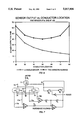
- FIG. 6 is a graph depicting the effect on the sensor output signal caused by sensor location with respect to a conductor.
- FIG. 7 is a schematic diagram depicting one embodiment of a feedback control circuit constructed in accordance with this invention.
- FIG. 3 shows a schematic diagram of one embodiment of this invention in which MOS switching transistor 30 is shown having a control gate 34, its drain connected to a positive voltage supply VCC, and its source connected to terminal 32a.
- Load device 31 is shown having one terminal connected to ground, and the second terminal connected to terminal 32b. Connected between terminals 32a and 32b is wire 35, for example a bonding wire commonly used in semiconductor applications.
- Bonding wire 35 is formed to serve as an element of Hall effect current sense device 100. Placement of bonding wire 35 in close proximity to the Hall sense device is essential to obtaining the maximum sensitivity, since load current between terminals 32a and 32b along wire 35 establishes a magnetic field that decreases in intensity as the distance from wire 35 increases. At a specific distance from wire 35, the strength of the magnetic field is directly proportional to the magnitude of the current in wire 35, and thus Hall effect device 100 provides an indication of the strength of the magnetic field and thus the magnitude of the current through wire 35. Polarity of the magnetic field is determined by the direction of current in wire 35. Thus, Hall effect device 100 also provides an indication of the direction of current through wire 35.
- FIG. 4 is a cross-sectional view of one embodiment of Hall effect current sensing device 100 of FIG. 3.
- Hall effect current sensing device 100 includes Hall effect sensors 102a and 102b located within a semiconductor substrate 101. Attached or at least placed in close proximity to semiconductor substrate 101 between Hall effect sensors 102a and 102b is wire 15. The dot contained in wire 15 indicates that current flow through wire 15 is out of the page, and thus magnetic flux lines are generated from Hall sensor 102a to Hall sensor 102b, as shown.
- FIG. 5 shows another view of the structure of FIG. 4. Shown in FIG. 5 is bonding pad 104 which is formed on substrate 101 in order to bond wire 15 to hold it in place, as desired. Naturally, if desired, a suitable insulation layer (not shown) is formed under wire 15 (FIG. 4) or under bonding pad 104 (FIG. 5).
- a load current switching device 120 such as MOSFET 30 of FIG. 3, on the same piece of semiconductor material as Hall effect device 100.
- switching device 120 is a MOSFET fabricated in active area 109 having its drain connected to bonding pad 122 for connection to an external load. Its source is connected to bonding pad 121 for the attachment of one end of wire 15 which is held in place on bonding pad 104 between Hall effect sensors 102a and 102b.
- Substrate 101 also includes active area 110 which contains suitable electronic circuitry for translating, if desired, the Hall effect current sensing device output signal for use, for example, as a feedback signal to control the magnitude of the load current. As shown in FIG.
- Hall effect sensors 102a and 102b provide their output signals via leads 124a and 124b to electronic control circuitry contained within active region 110. This electronic control circuitry then provides a control signal via lead 123 to the gate of MOSFET 120. A more detailed description of one embodiment of control circuitry such as formed within active region 110 is described later with reference to FIG. 7.
- a load current structure including a current sensing means, is provided which is easily fabricated using well known semiconductor principals.
- a detailed description of structure and operation of Hall effect devices is provided in "Integrated Semiconductor Magnetic Field Sensors," Baltes and Popovic, proceedings of the IEEE, Volume 74, No. 8, August 1968, pages 1107-1132, which is hereby incorporated by reference.
- the common-mode voltage of the Hall effect sensors is fixed and independent of power supply voltage and load voltage transients. This significantly reduces settling time of the current sensing signal in response to transients in the load current. Also, the use of a wire in order to form a portion of the current sensing device does not appreciably increase the voltage drop across the combination of the load current switching device and load current sensor.
- a Hall effect sensing device in accordance with the teachings of this invention allows for accurate measurement of significantly smaller currents (for example, as low as approximately 10 amperes) as compared with prior art techniques utilizing external sensors which, when packaged, increase the spacing to the current-carrying wire by at least an order of magnitude and decrease the sensitivity accordingly.
- orientation of a packaged Hall effect sensor with respect to the current carrying wire must be permanently fixed by some means so that the sensitivity does not change because of spacing changes or flux angle changes.
- the use of two sensors 102a and 102b (FIGS.
- a single Hall effect sensing element can be used, for example, either one of Hall effect sensors 102a or 102b of FIGS. 4 and 5.
- teachings of this invention is suitable for use with any type of semiconductor current sources and sinks, e.g. MOSFETs, Bipolar transistors, SCRs, Zener diodes, etc, which are, in one embodiment, fabricated in active area 109 of substrate 101 (FIG. 5) together with additional circuitry formed in active area 110 for manipulating the signals received from the Hall effect sensors, for example, to provide feedback to current control devices within active area 109.
- r the perpendicular distance from the conductor.
- r the perpendicular distance from the conductor.
- Vout the sum of the voltages from the two Hall effect sensors
- r1 the perpendicular distance between the conductor and the first Hall effect sensor
- r2 the perpendicular distance between the conductor and the second Hall effect sensor.
- K1 1000, as an arbitrary gain factor.
- K2 100, as an arbitrary distance between the two Hall effect sensors.
- Vout For various values of r1, the following values of Vout are determined.
- FIG. 7 illustrates one embodiment of this invention where a power MOSFET 71 is controlled by the output signal from two Hall sensors 72 and 73 which measure the intensity of the magnetic field produced by load current I L flowing through bonding wire 74 from MOSFET 71.
- Hall sensors 72 and 73 receive a bias voltage from terminal 75 and provide differential output signals on lead pairs 76a, 76b and 77a, 77b which are connected to the non-inverting and inverting input leads of amplifiers A1 and A2, respectively.
- Amplifiers A1 and A2 serve two functions. The first is to prevent loading of Hall sensors 72 and 73 and the second is to provide sufficient voltage gain between Hall sensors 72 and 73 and summing resistors R1 and R2.
- Amplifiers 72 and 73 may be, for example, instrumentation amplifiers.
- Operational amplifier A3, in conjunction with resistors R1, R2, and R3, sums the output signals of amplifiers A1 and A2. Since the summing function is inverting, the output signal of amplifier A3 ranges between some positive voltage when current I L through MOSFET 71 is zero to more negative voltages with increasing current I L .
- switch S1 in the linear position switch position as shown in FIG.
- the latch composed of NAND gates G1 and G2 is used by putting switch S1 in the latching position (switch position opposite that shown in FIG. 7).
- the reference voltage on the non-inverting input lead of amplifier A3 determines the I L current level at which the logic threshold of gate G1 will be reached, setting the latch and turning off MOSFET 71.
- Activation of MOSFET 71 is restored by providing a reset signal through inverter I to gate G2.
Abstract
Description
V=K1/r; (2)
Vout=K1(1/r1+1/r2); (3)
r2K2-r1 (4)
Vout=K1(1/r1+1/(K2-r1)) (5)
              TABLE 1
______________________________________
Scaled Vout
rl      (from equation (5))
                      (from equation (2))
______________________________________
20      62.50         50.00
30      47.62         33.33
40      41.67         25.00
50      40.00         20.00
60      41.67         16.67
70      47.62         14.29
80      62.50         12.50
______________________________________
              TABLE 2
______________________________________
Deviation from midpoint
rl          Two Sensors
                       One sensor
______________________________________
30          19.05%      66.67%
70          19.05%     -28.75%
______________________________________
              TABLE 3
______________________________________
Ratio of maximum to minimum Vout
Two Sensors    One Sensor
______________________________________
1.19           2.33
______________________________________
Claims (12)
Priority Applications (1)
| Application Number | Priority Date | Filing Date | Title |
|---|---|---|---|
| US07/340,445 US5017804A (en) | 1987-07-23 | 1989-04-19 | Hall sensing of bond wire current |
Applications Claiming Priority (2)
| Application Number | Priority Date | Filing Date | Title |
|---|---|---|---|
| US7678887A | 1987-07-23 | 1987-07-23 | |
| US07/340,445 US5017804A (en) | 1987-07-23 | 1989-04-19 | Hall sensing of bond wire current |
Related Parent Applications (1)
| Application Number | Title | Priority Date | Filing Date |
|---|---|---|---|
| US7678887A Continuation-In-Part | 1987-07-23 | 1987-07-23 |
Publications (1)
| Publication Number | Publication Date |
|---|---|
| US5017804A true US5017804A (en) | 1991-05-21 |
Family
ID=26758478
Family Applications (1)
| Application Number | Title | Priority Date | Filing Date |
|---|---|---|---|
| US07/340,445 Expired - Lifetime US5017804A (en) | 1987-07-23 | 1989-04-19 | Hall sensing of bond wire current |
Country Status (1)
| Country | Link |
|---|---|
| US (1) | US5017804A (en) |
Cited By (20)
| Publication number | Priority date | Publication date | Assignee | Title |
|---|---|---|---|---|
| WO1996022539A1 (en) * | 1995-01-18 | 1996-07-25 | Horstmann Timers & Controls Limited | Electricity measurement apparatus and method |
| WO1996028738A1 (en) * | 1995-03-16 | 1996-09-19 | Horstmann Timers & Controls Limited | Electricity measurement apparatus |
| US5640090A (en) * | 1995-01-31 | 1997-06-17 | Mitsumi Electric Company, Ltd. | Sensor IC |
| WO2000054063A1 (en) * | 1999-03-11 | 2000-09-14 | Fraunhofer-Gesellschaft zur Förderung der angewandten Forschung e.V. | Device and method for measuring an electric current |
| WO2000060366A1 (en) * | 1999-03-31 | 2000-10-12 | Aeg Niederspannungstechnik Gmbh & Co. Kg | Current meter |
| DE10045563B4 (en) * | 1999-09-16 | 2004-09-09 | International Rectifier Corp., El Segundo | The power semiconductor module assembly |
| US20090058575A1 (en) * | 2007-09-05 | 2009-03-05 | The Smart Pill Corporation | Magnetic activation and deactivation circuit and system |
| US20090224754A1 (en) * | 2008-03-06 | 2009-09-10 | Jonathan Lamarre | Two-terminal linear sensor |
| US20100156394A1 (en) * | 2008-12-18 | 2010-06-24 | Infineon Technologies Ag | Magnetic field current sensors |
| US20110204887A1 (en) * | 2010-02-24 | 2011-08-25 | Infineon Technologies Ag | Current sensors and methods |
| US20120112733A1 (en) * | 2010-11-09 | 2012-05-10 | Texas Instruments Incorporated | Hall Effect Device |
| US8283742B2 (en) | 2010-08-31 | 2012-10-09 | Infineon Technologies, A.G. | Thin-wafer current sensors |
| US20140015533A1 (en) * | 2011-03-29 | 2014-01-16 | Continental Teves Ag & Co. Ohg | Current sensor |
| US8680843B2 (en) | 2010-06-10 | 2014-03-25 | Infineon Technologies Ag | Magnetic field current sensors |
| US8760149B2 (en) | 2010-04-08 | 2014-06-24 | Infineon Technologies Ag | Magnetic field current sensors |
| US8963536B2 (en) | 2011-04-14 | 2015-02-24 | Infineon Technologies Ag | Current sensors, systems and methods for sensing current in a conductor |
| US8975889B2 (en) | 2011-01-24 | 2015-03-10 | Infineon Technologies Ag | Current difference sensors, systems and methods |
| US9476915B2 (en) | 2010-12-09 | 2016-10-25 | Infineon Technologies Ag | Magnetic field current sensors |
| US20170059628A1 (en) * | 2015-08-31 | 2017-03-02 | Boe Technology Group Co., Ltd. | Power detection apparatus |
| IT201900016193A1 (en) * | 2019-09-12 | 2021-03-12 | St Microelectronics Srl | POWER DEVICE, SYSTEM INCLUDING THE POWER DEVICE, METHOD OF MANUFACTURING THE POWER DEVICE AND METHOD OF CONTROL OF THE POWER DEVICE |
Citations (15)
| Publication number | Priority date | Publication date | Assignee | Title |
|---|---|---|---|---|
| US3284703A (en) * | 1963-01-14 | 1966-11-08 | Canadair Ltd | Hall effect device utilized to compensate for variable induced fields in other sensors |
| US3296573A (en) * | 1967-01-03 | Substrate configurations for hall elements | ||
| US3667000A (en) * | 1968-08-31 | 1972-05-30 | Philips Corp | Integrated hall-effect device |
| US3693085A (en) * | 1971-07-15 | 1972-09-19 | Gen Motors Corp | System for calibrated high level current measurement using a magnetic field responsive transistor |
| US4011469A (en) * | 1973-07-09 | 1977-03-08 | U.S. Philips Corporation | Hall effect-switching device |
| US4099238A (en) * | 1975-04-07 | 1978-07-04 | Ricoh Company, Ltd. | Apparatus for determining a magnetic field |
| US4283643A (en) * | 1979-05-25 | 1981-08-11 | Electric Power Research Institute, Inc. | Hall sensing apparatus |
| US4371837A (en) * | 1979-11-13 | 1983-02-01 | American Can Company | Temperature compensated input power and output offset circuits for a hall effect transducer |
| US4553084A (en) * | 1984-04-02 | 1985-11-12 | Motorola, Inc. | Current sensing circuit |
| US4607271A (en) * | 1982-11-22 | 1986-08-19 | IGZ Landis & Gyr Zug AG | Magnetic field sensor |
| US4616207A (en) * | 1984-10-12 | 1986-10-07 | Gould Inc. | Electric fuse holder having a Hall-effect current sensor |
| US4625562A (en) * | 1984-06-08 | 1986-12-02 | Matsushita Electric Industrial Co., Ltd. | Amorphous magnetic alloy sensor |
| US4705964A (en) * | 1986-09-29 | 1987-11-10 | Sprague Electric Company | Integrated circuit hall switch with adjustable operate point |
| US4760285A (en) * | 1987-03-30 | 1988-07-26 | Honeywell Inc. | Hall effect device with epitaxal layer resistive means for providing temperature independent sensitivity |
| JPS63234578A (en) * | 1987-03-24 | 1988-09-29 | Matsushita Electric Ind Co Ltd | Hall effect device |
-
1989
- 1989-04-19 US US07/340,445 patent/US5017804A/en not_active Expired - Lifetime
Patent Citations (15)
| Publication number | Priority date | Publication date | Assignee | Title |
|---|---|---|---|---|
| US3296573A (en) * | 1967-01-03 | Substrate configurations for hall elements | ||
| US3284703A (en) * | 1963-01-14 | 1966-11-08 | Canadair Ltd | Hall effect device utilized to compensate for variable induced fields in other sensors |
| US3667000A (en) * | 1968-08-31 | 1972-05-30 | Philips Corp | Integrated hall-effect device |
| US3693085A (en) * | 1971-07-15 | 1972-09-19 | Gen Motors Corp | System for calibrated high level current measurement using a magnetic field responsive transistor |
| US4011469A (en) * | 1973-07-09 | 1977-03-08 | U.S. Philips Corporation | Hall effect-switching device |
| US4099238A (en) * | 1975-04-07 | 1978-07-04 | Ricoh Company, Ltd. | Apparatus for determining a magnetic field |
| US4283643A (en) * | 1979-05-25 | 1981-08-11 | Electric Power Research Institute, Inc. | Hall sensing apparatus |
| US4371837A (en) * | 1979-11-13 | 1983-02-01 | American Can Company | Temperature compensated input power and output offset circuits for a hall effect transducer |
| US4607271A (en) * | 1982-11-22 | 1986-08-19 | IGZ Landis & Gyr Zug AG | Magnetic field sensor |
| US4553084A (en) * | 1984-04-02 | 1985-11-12 | Motorola, Inc. | Current sensing circuit |
| US4625562A (en) * | 1984-06-08 | 1986-12-02 | Matsushita Electric Industrial Co., Ltd. | Amorphous magnetic alloy sensor |
| US4616207A (en) * | 1984-10-12 | 1986-10-07 | Gould Inc. | Electric fuse holder having a Hall-effect current sensor |
| US4705964A (en) * | 1986-09-29 | 1987-11-10 | Sprague Electric Company | Integrated circuit hall switch with adjustable operate point |
| JPS63234578A (en) * | 1987-03-24 | 1988-09-29 | Matsushita Electric Ind Co Ltd | Hall effect device |
| US4760285A (en) * | 1987-03-30 | 1988-07-26 | Honeywell Inc. | Hall effect device with epitaxal layer resistive means for providing temperature independent sensitivity |
Non-Patent Citations (2)
| Title |
|---|
| Baltes and Popovic Proceedings of the IEEE, "Integrated Semiconductor Magnetic Field Sensors" (Aug. 1986), pp. 1107-1132. |
| Baltes and Popovic Proceedings of the IEEE, Integrated Semiconductor Magnetic Field Sensors (Aug. 1986), pp. 1107 1132. * |
Cited By (37)
| Publication number | Priority date | Publication date | Assignee | Title |
|---|---|---|---|---|
| WO1996022539A1 (en) * | 1995-01-18 | 1996-07-25 | Horstmann Timers & Controls Limited | Electricity measurement apparatus and method |
| US6040690A (en) * | 1995-01-18 | 2000-03-21 | Horstmann Timers & Controls Limited | Electricity measurement using two conductors |
| US5640090A (en) * | 1995-01-31 | 1997-06-17 | Mitsumi Electric Company, Ltd. | Sensor IC |
| WO1996028738A1 (en) * | 1995-03-16 | 1996-09-19 | Horstmann Timers & Controls Limited | Electricity measurement apparatus |
| WO2000054063A1 (en) * | 1999-03-11 | 2000-09-14 | Fraunhofer-Gesellschaft zur Förderung der angewandten Forschung e.V. | Device and method for measuring an electric current |
| WO2000060366A1 (en) * | 1999-03-31 | 2000-10-12 | Aeg Niederspannungstechnik Gmbh & Co. Kg | Current meter |
| DE10045563B4 (en) * | 1999-09-16 | 2004-09-09 | International Rectifier Corp., El Segundo | The power semiconductor module assembly |
| US20090058575A1 (en) * | 2007-09-05 | 2009-03-05 | The Smart Pill Corporation | Magnetic activation and deactivation circuit and system |
| WO2009032064A3 (en) * | 2007-09-05 | 2009-04-30 | Smart Pill Corp | Magnetic activation and deactivation circuit and system |
| US7834725B2 (en) | 2007-09-05 | 2010-11-16 | The Smartpill Corporation | Magnetic activation and deactivation circuit and system |
| US20090224754A1 (en) * | 2008-03-06 | 2009-09-10 | Jonathan Lamarre | Two-terminal linear sensor |
| US8773123B2 (en) | 2008-03-06 | 2014-07-08 | Allegro Microsystems, Llc | Two-terminal linear sensor |
| US8054071B2 (en) * | 2008-03-06 | 2011-11-08 | Allegro Microsystems, Inc. | Two-terminal linear sensor |
| US20100156394A1 (en) * | 2008-12-18 | 2010-06-24 | Infineon Technologies Ag | Magnetic field current sensors |
| US9733279B2 (en) | 2008-12-18 | 2017-08-15 | Infineon Technologies Ag | Magnetic field current sensors |
| US9222992B2 (en) | 2008-12-18 | 2015-12-29 | Infineon Technologies Ag | Magnetic field current sensors |
| US9865802B2 (en) | 2010-02-24 | 2018-01-09 | Infineon Technologies Ag | Current sensors and methods |
| US20110204887A1 (en) * | 2010-02-24 | 2011-08-25 | Infineon Technologies Ag | Current sensors and methods |
| US8717016B2 (en) | 2010-02-24 | 2014-05-06 | Infineon Technologies Ag | Current sensors and methods |
| US9983238B2 (en) | 2010-04-08 | 2018-05-29 | Infineon Technologies Ag | Magnetic field current sensors having enhanced current density regions |
| US8760149B2 (en) | 2010-04-08 | 2014-06-24 | Infineon Technologies Ag | Magnetic field current sensors |
| US8680843B2 (en) | 2010-06-10 | 2014-03-25 | Infineon Technologies Ag | Magnetic field current sensors |
| US8283742B2 (en) | 2010-08-31 | 2012-10-09 | Infineon Technologies, A.G. | Thin-wafer current sensors |
| US9029966B2 (en) | 2010-08-31 | 2015-05-12 | Infineon Technologies Ag | Thin-wafer current sensors |
| US8679895B2 (en) | 2010-08-31 | 2014-03-25 | Infineon Technologies Ag | Method of making thin-wafer current sensors |
| US20120112733A1 (en) * | 2010-11-09 | 2012-05-10 | Texas Instruments Incorporated | Hall Effect Device |
| US9013167B2 (en) * | 2010-11-09 | 2015-04-21 | Texas Instruments Incorporated | Hall effect device having voltage based biasing for temperature compensation |
| US9476915B2 (en) | 2010-12-09 | 2016-10-25 | Infineon Technologies Ag | Magnetic field current sensors |
| US9678172B2 (en) | 2011-01-24 | 2017-06-13 | Infineon Technologies Ag | Current difference sensors, systems and methods |
| US8975889B2 (en) | 2011-01-24 | 2015-03-10 | Infineon Technologies Ag | Current difference sensors, systems and methods |
| US10488445B2 (en) | 2011-01-24 | 2019-11-26 | Infineon Technologies Ag | Current difference sensors, systems and methods |
| US20140015533A1 (en) * | 2011-03-29 | 2014-01-16 | Continental Teves Ag & Co. Ohg | Current sensor |
| US8963536B2 (en) | 2011-04-14 | 2015-02-24 | Infineon Technologies Ag | Current sensors, systems and methods for sensing current in a conductor |
| US9395423B2 (en) | 2011-04-14 | 2016-07-19 | Infineon Technologies Ag | Current sensors, systems and methods for sensing current in a conductor |
| US20170059628A1 (en) * | 2015-08-31 | 2017-03-02 | Boe Technology Group Co., Ltd. | Power detection apparatus |
| IT201900016193A1 (en) * | 2019-09-12 | 2021-03-12 | St Microelectronics Srl | POWER DEVICE, SYSTEM INCLUDING THE POWER DEVICE, METHOD OF MANUFACTURING THE POWER DEVICE AND METHOD OF CONTROL OF THE POWER DEVICE |
| US11552191B2 (en) | 2019-09-12 | 2023-01-10 | Stmicroelectronics S.R.L. | Power device, system including the power device, method for manufacturing the power device, and method for controlling the power device |
Similar Documents
| Publication | Publication Date | Title |
|---|---|---|
| US5017804A (en) | Hall sensing of bond wire current | |
| KR930010102B1 (en) | Transistor provided with a current detecting function | |
| US6154027A (en) | Monolithic magnetic sensor having externally adjustable temperature compensation | |
| US7952333B2 (en) | Circuit and method for determining current in a load | |
| US6995555B2 (en) | Apparatus and method for determining a current through a power semiconductor component | |
| US4910455A (en) | Non-intrusive current measuring circuit | |
| US6433615B2 (en) | Semiconductor device having a sensor with the temperature compensation function | |
| US11789095B2 (en) | Current sensor, magnetic sensor and circuit | |
| EP0596473A1 (en) | Circuit for monitoring the drain current of a MOSFET | |
| US4875011A (en) | Magnetic sensor using integrated silicon Hall effect elements formed on the (100) plane of a silicon substrate | |
| JPS6144360B2 (en) | ||
| US20200363463A1 (en) | Power semiconductor device with integrated current measurement | |
| US20060158182A1 (en) | Magnetic sensor circuit and semiconductor device | |
| CN113411074A (en) | Hall sensor switch and electronic equipment | |
| JPH0661432A (en) | Semiconductor device | |
| EP0449443B1 (en) | Hot wire air flow meter | |
| CA1195735A (en) | In-phase voltage elimination circuit for hall element | |
| US5801533A (en) | Method and apparatus with cascode biasing magneto field effect transistors for improved sensitivity and amplification | |
| EP0157447B1 (en) | Differential amplifier | |
| US5663574A (en) | Power semiconductor component with monolithically integrated sensor arrangement as well as manufacture and employment thereof | |
| JPH06194433A (en) | Magnetometer | |
| US6861717B2 (en) | Device for defecting a magnetic field, magnetic field measure and current meter | |
| US4965547A (en) | Signal converter circuit | |
| US6777766B2 (en) | Device for sensing a magnetic field, magnetic field meter and an ammeter | |
| JPWO2019065173A1 (en) | Power module and DC-DC converter |
Legal Events
| Date | Code | Title | Description |
|---|---|---|---|
| AS | Assignment |
Owner name: SILICONIX, INCORPORATED, 2201 LAURELWOOD, ROAD, SA Free format text: ASSIGNMENT OF ASSIGNORS INTEREST.;ASSIGNORS:HARNDEN, JAMES A.;HILL, LORIMER K.;REEL/FRAME:005110/0534 Effective date: 19890420 |
|
| AS | Assignment |
Owner name: INTERNATIONAL RECTIFIER CORPORATION, A DE CORP. Free format text: SECURITY INTEREST;ASSIGNOR:SILICONIX INCORPORATED, A DE CORP.;REEL/FRAME:005562/0082 Effective date: 19901221 |
|
| STCF | Information on status: patent grant |
Free format text: PATENTED CASE |
|
| AS | Assignment |
Owner name: SILICONIX INCORPORATED, A CORP. OF DE Free format text: RELEASE BY SECURED PARTY, RECORDED AT REEL 5562, FRAME 0082, ON 12-28-90;ASSIGNOR:INTERNATIONAL RECTIFIER CORPORATION;REEL/FRAME:005660/0221 Effective date: 19910320 |
|
| CC | Certificate of correction | ||
| FPAY | Fee payment |
Year of fee payment: 4 |
|
| FPAY | Fee payment |
Year of fee payment: 8 |
|
| FPAY | Fee payment |
Year of fee payment: 12 |