US5029984A - Liquid crystal display device - Google Patents
Liquid crystal display device Download PDFInfo
- Publication number
- US5029984A US5029984A US07/307,739 US30773989A US5029984A US 5029984 A US5029984 A US 5029984A US 30773989 A US30773989 A US 30773989A US 5029984 A US5029984 A US 5029984A
- Authority
- US
- United States
- Prior art keywords
- liquid crystal
- crystal display
- display panel
- circuit board
- drive circuit
- Prior art date
- Legal status (The legal status is an assumption and is not a legal conclusion. Google has not performed a legal analysis and makes no representation as to the accuracy of the status listed.)
- Expired - Lifetime
Links
Images


Classifications
-
- G—PHYSICS
- G02—OPTICS
- G02F—OPTICAL DEVICES OR ARRANGEMENTS FOR THE CONTROL OF LIGHT BY MODIFICATION OF THE OPTICAL PROPERTIES OF THE MEDIA OF THE ELEMENTS INVOLVED THEREIN; NON-LINEAR OPTICS; FREQUENCY-CHANGING OF LIGHT; OPTICAL LOGIC ELEMENTS; OPTICAL ANALOGUE/DIGITAL CONVERTERS
- G02F1/00—Devices or arrangements for the control of the intensity, colour, phase, polarisation or direction of light arriving from an independent light source, e.g. switching, gating or modulating; Non-linear optics
- G02F1/01—Devices or arrangements for the control of the intensity, colour, phase, polarisation or direction of light arriving from an independent light source, e.g. switching, gating or modulating; Non-linear optics for the control of the intensity, phase, polarisation or colour
- G02F1/13—Devices or arrangements for the control of the intensity, colour, phase, polarisation or direction of light arriving from an independent light source, e.g. switching, gating or modulating; Non-linear optics for the control of the intensity, phase, polarisation or colour based on liquid crystals, e.g. single liquid crystal display cells
- G02F1/133—Constructional arrangements; Operation of liquid crystal cells; Circuit arrangements
- G02F1/1333—Constructional arrangements; Manufacturing methods
- G02F1/1345—Conductors connecting electrodes to cell terminals
- G02F1/13452—Conductors connecting driver circuitry and terminals of panels
-
- H—ELECTRICITY
- H01—ELECTRIC ELEMENTS
- H01L—SEMICONDUCTOR DEVICES NOT COVERED BY CLASS H10
- H01L25/00—Assemblies consisting of a plurality of individual semiconductor or other solid state devices ; Multistep manufacturing processes thereof
- H01L25/03—Assemblies consisting of a plurality of individual semiconductor or other solid state devices ; Multistep manufacturing processes thereof all the devices being of a type provided for in the same subgroup of groups H01L27/00 - H01L33/00, or in a single subclass of H10K, H10N, e.g. assemblies of rectifier diodes
- H01L25/04—Assemblies consisting of a plurality of individual semiconductor or other solid state devices ; Multistep manufacturing processes thereof all the devices being of a type provided for in the same subgroup of groups H01L27/00 - H01L33/00, or in a single subclass of H10K, H10N, e.g. assemblies of rectifier diodes the devices not having separate containers
- H01L25/065—Assemblies consisting of a plurality of individual semiconductor or other solid state devices ; Multistep manufacturing processes thereof all the devices being of a type provided for in the same subgroup of groups H01L27/00 - H01L33/00, or in a single subclass of H10K, H10N, e.g. assemblies of rectifier diodes the devices not having separate containers the devices being of a type provided for in group H01L27/00
- H01L25/0652—Assemblies consisting of a plurality of individual semiconductor or other solid state devices ; Multistep manufacturing processes thereof all the devices being of a type provided for in the same subgroup of groups H01L27/00 - H01L33/00, or in a single subclass of H10K, H10N, e.g. assemblies of rectifier diodes the devices not having separate containers the devices being of a type provided for in group H01L27/00 the devices being arranged next and on each other, i.e. mixed assemblies
-
- H—ELECTRICITY
- H01—ELECTRIC ELEMENTS
- H01R—ELECTRICALLY-CONDUCTIVE CONNECTIONS; STRUCTURAL ASSOCIATIONS OF A PLURALITY OF MUTUALLY-INSULATED ELECTRICAL CONNECTING ELEMENTS; COUPLING DEVICES; CURRENT COLLECTORS
- H01R12/00—Structural associations of a plurality of mutually-insulated electrical connecting elements, specially adapted for printed circuits, e.g. printed circuit boards [PCB], flat or ribbon cables, or like generally planar structures, e.g. terminal strips, terminal blocks; Coupling devices specially adapted for printed circuits, flat or ribbon cables, or like generally planar structures; Terminals specially adapted for contact with, or insertion into, printed circuits, flat or ribbon cables, or like generally planar structures
- H01R12/70—Coupling devices
- H01R12/7076—Coupling devices for connection between PCB and component, e.g. display
-
- H—ELECTRICITY
- H01—ELECTRIC ELEMENTS
- H01L—SEMICONDUCTOR DEVICES NOT COVERED BY CLASS H10
- H01L2224/00—Indexing scheme for arrangements for connecting or disconnecting semiconductor or solid-state bodies and methods related thereto as covered by H01L24/00
- H01L2224/01—Means for bonding being attached to, or being formed on, the surface to be connected, e.g. chip-to-package, die-attach, "first-level" interconnects; Manufacturing methods related thereto
- H01L2224/42—Wire connectors; Manufacturing methods related thereto
- H01L2224/47—Structure, shape, material or disposition of the wire connectors after the connecting process
- H01L2224/49—Structure, shape, material or disposition of the wire connectors after the connecting process of a plurality of wire connectors
- H01L2224/491—Disposition
- H01L2224/4912—Layout
- H01L2224/49175—Parallel arrangements
-
- H—ELECTRICITY
- H01—ELECTRIC ELEMENTS
- H01L—SEMICONDUCTOR DEVICES NOT COVERED BY CLASS H10
- H01L2924/00—Indexing scheme for arrangements or methods for connecting or disconnecting semiconductor or solid-state bodies as covered by H01L24/00
- H01L2924/095—Indexing scheme for arrangements or methods for connecting or disconnecting semiconductor or solid-state bodies as covered by H01L24/00 with a principal constituent of the material being a combination of two or more materials provided in the groups H01L2924/013 - H01L2924/0715
- H01L2924/097—Glass-ceramics, e.g. devitrified glass
- H01L2924/09701—Low temperature co-fired ceramic [LTCC]
Definitions
- the present invention relates to a liquid crystal display device for use in a display for office automation equipment, computers, television receivers, or the like as a substitute for a cathode ray tube.
- CRTs cathode ray tubes
- LCDs cathode ray tubes
- FIG. 1 is a sectional view of a prior art liquid crystal display device disclosed, for example, in Japanese Laid-open Patent Publication No. 60-229089 and FIG. 2 is a perspective view of the same.
- reference numeral 1 denotes a liquid crystal display panel composed of two glass plates 2, 3 with a transparent conductive film formed thereon, a sealant 4 for joining the glass plates 2, 3 together at their peripheral portions, liquid crystals 5, and polarizing plates 6 stuck onto the front and the back of the glass plates 2, 3.
- thin-film transistors are formed on the glass plate 3 and of a color display, a color filter is formed on the glass plate 2 or 3.
- Reference numeral 7 denotes a drive IC for supplying an electric signal necessary for the liquid crystal display panel 1
- 8 denotes a protection coating for moisture proofing and mechanical protection and reinforcement of the drive IC 7.
- Reference numeral 10 denotes a circuit board having a plurality of drive ICs mounted thereon and having a conductive pattern providing a drive circuit for the liquid crystal display panel formed thereon.
- a flexible printed board formed of a polyimide film is normally used for the circuit board 10 and it is provided with a reinforcement lining plate 9 stuck onto its back side.
- circuit board 10 For connecting the circuit board 10 with the liquid crystal display panel 1, such methods are used as soldering, thermocompression bonding using an anisotropic conductive film and so on, mechanical pressure joining, or the like.
- a transparent conductive film 11 On a transparent conductive film 11, there is provided Ni or Ni/Au coating, pretinning or the like, according to the need.
- the circuit boards 10a, 10b, 10c connected with each side of the liquid crystal display panel 1 are interconnected with each other by means of a flexible printed board, a flat cable, wire bonding, or the like.
- Reference numeral 12 denotes a light box casing fixed to the back side of the glass plate 3 and contains a lamp 13, a reflecting plate 14, and a light diffusing plate 15.
- the liquid crystal display device organized as described above has the circuit board 10, together with the reinforcement lining plate 9, stuck to the periphery of the liquid crystal display panel 1, it becomes larger in size than the liquid crystal display surface by the width of the circuit board 10 disposed at the periphery, and therefore miniaturization of the device cannot be attained.
- the flexible printed board of a polyimide film tends to produce large changes in its dimensions by the effects of temperature and moisture, causing the terminals of the circuit board 10 to deviate from the positions for connection with the liquid crystal display panel 1 at each edge thereof and making the alignment difficult.
- the number of times of alignment performed for terminal connection and the number of connections increase, and therefore, a longer processing time is required and automatic assembling becomes difficult.
- FIG. 3 is a partial plan view of terminal portions to be connected with a drive circuit module of a liquid crystal display panel incorporating such thin-film transistors therein.
- reference numeral 1 denotes the liquid crystal display panel
- 3 denotes an array substrate formed of a glass plate with thin-film transistors provided thereon
- 2 denotes a counter substrate formed of a glass plate with a transparent electrode provided all over its surface
- 4 denotes a seal portion for joining the array substrate 3 and the counter electrode 2 together, thereby forming them into a liquid crystal cell.
- Reference numeral 21 denotes a group of transparent electrode terminals led out from the source electrodes of the thin-film transistors and reference numeral 22 denotes a group of transparent electrode terminals led out from the gate electrodes of the same. While one group of transparent electrode terminals 21 are connected with a group of output terminals of a drive circuit module with a plurality of ICs for image data processing mounted thereon, the other group of transparent electrode terminals 22 are connected with a group of output terminals of another drive circuit module with a plurality of ICs for linear scanning circuits mounted thereon.
- FIG. 4(a) and FIG. 4(b) show an example of connection of a liquid crystal display panel with drive circuit modules in an active matrix liquid crystal display device disclosed in Japanese Laid-open Patent Publication No. 60-229090.
- Denoted by 1 to 4 are the same parts as those denoted by the same reference numerals in the liquid crystal display panel shown in FIG. 3.
- Reference numeral 5 denotes liquid crystals sandwiched in between the array substrate 3 and the counter substrate 2
- 10 denotes a circuit board made of ceramic, glass, glass epoxy, glass polyimide, or the like
- 7 denotes an IC chip mounted on the circuit board
- 23 denotes a bonding wire connecting the circuit board 10 with the IC chip 7, and these parts together constitute a drive circuit module 18.
- the transparent electrode terminals (not shown) formed on the array substrate 3 are provided with Au coating or the like in advance, and the drive circuit module 18 is connected with the array substrate 3 by means of wire bonding 28. Further, the drive circuit modules 18a, 18b, 18c, and 18d are interconnected with each other by means of wire bonding, a flat cable, or a flexible printed board (all of which are not shown).
- the active matrix liquid crystal display device organized as described above has the configuration in which the drive circuit module 18 is fixedly stuck onto the array substrate 3, the array substrate is required to have a size large enough to provide the region on which the drive circuit module 18 is fixed in addition to the area in which the groups of the transparent electrode terminals are disposed. Thus, there has been a problem that the external size of the device becomes too large for the display area.
- the ICs for image data processing and the ICs for linear scanning circuits, mounted on the drive circuit modules 18 for supplying signals to the opposing groups of the transparent electrode terminals 21 or 22 on the source side or the gate side are each of the same function but the positions of the output terminals are inverted, and therefore, chips in which output sequences rotate in the opposite directions, so-called mirror chips, are required.
- the drive circuit modules 18 must be classified according to their uses. Efficiency of the assembly work has therefore been impaired.
- the groups of terminals on the circuit board 10 constituting the drive circuit modules 18 are common for all the four sides of the circuit board or to be common for the upper and lower two sides and for the left and right two sides of the circuit board, as in the prior art liquid crystal display device shown in FIG. 1 and FIG. 2.
- the drive circuit modules in common can be used for image data processing circuits at the upper and the lower sides of the liquid crystal display panel and the drive circuit modules in common can be used for linear scanning circuits at the left and the right sides of the liquid crystal display panel.
- the groups of the terminals connected with the array substrate 3 are provided at the opposing two edges of the periphery of the substrate, the size of the circuit board becomes still larger than that in the liquid crystal display device shown in FIG. 4, and therefore, the array substrate 3 for having the drive circuit module 18 fixedly stuck thereto must also be made still larger, thus hindering the miniaturization of the device. Further, there has been a problem that the number of wires for forming the groups of terminals at two sides becomes very large, whereby multilayer wiring have had to be provided.
- an object of the present invention is to provide a liquid crystal display device in which operating efficiency in the assembly work and the yield rate of the drive circuit boards are improved and the miniaturization of the device can be achieved.
- the liquid crystal display device in a liquid crystal display device with a circuit board including drive ICs and drive circuits connected at the peripheral portion of a liquid crystal display panel, the liquid crystal display device according to the present invention has the circuit board disposed behind the liquid crystal display panel and comprises a connecting member in film form for electrically connecting the panel with the circuit board.
- the circuit board connected to the liquid crystal display panel does not protrude from the periphery of the panel, thereby enabling miniaturization of the liquid crystal display device.
- Another object of the present invention is to provide an active matrix liquid crystal display device, wherein, in connecting opposing drive circuit modules on each of the source side and the gate side to the liquid crystal display panel, drive circuit modules composed of ICs of the same type and circuit boards of the same type are used, whereby the assembly process is simplified, the yield rate in the assembly work is improved, and further, miniaturization of the device is achieved.
- FIG. 1 is a sectional view of a prior art liquid crystal display device
- FIG. 2 is a perspective view of the same
- FIG. 3 is a partial plan view of a group of terminals of a liquid crystal display panel incorporating thin-film transistors therein;
- FIG. 4(a) and FIG. 4(b) are a plan view and a sectional view showing a liquid crystal display panel and drive circuit modules of a prior art active matrix liquid crystal display device;
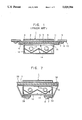
- FIG. 5 is a sectional view of a liquid crystal display device according to an embodiment of the present invention.
- FIG. 6 is a perspective view of the same
- FIG. 7 is a sectional view of a liquid crystal display device according to a second embodiment
- FIG. 8 is a partially sectional view of a liquid crystal display device according to a third embodiment of the present invention of which drive circuit modules and a liquid crystal display panel are connected with each other;
- FIG. 9 and FIG. 10 are a front view of a drive circuit module for a liquid crystal display device according to a fourth embodiment of the present invention, and a partially sectional view of the same of which drive circuit modules and a liquid crystal display panel are connected with each other.
- FIG. 5 is a sectional view of a liquid crystal display device according to the present invention and FIG. 6 is a perspective view of the same.
- reference numeral 1 denotes a liquid crystal display panel of the same structure as that of the prior art
- 10 denotes a rigid circuit board of glass epoxy, heat-resisting glass epoxy, glass polyimide, or the like, and on which are disposed, the same as in the prior art example, drive ICs 7, protecting coatings 8, and conductive patterns 31.
- the circuit board 10 is disposed behind the liquid crystal display panel 1 perpendicularly to the same, stuck to a light box casing 12 through a heat insulating member 33 made of a non-heat-conductive material such as foam plastics.
- Reference numeral 32 denotes a connecting member in film form which electrically connects a transparent conductive film 11 formed on the glass plate as a constituent of the liquid crystal display panel 1 with the circuit board 10.
- a plurality of drive ICs 7 are stuck onto a heat-resisting glass epoxy substrate of a thickness of 0.5 to 1.0 mm, and then wire bonding is performed and protecting coatings 8 for improving moisture resistance, mechanical protection, and reinforcement are provided therefor, and thereby, a circuit board 10 for driving a liquid crystal display panel is formed.
- a heat seal connector which is formed by using a 35 ⁇ m-thick polyester film as the base and providing thereon by pattern printing conductive portions made up of a layer of thermosetting resin including silver powder or carbon powder and a layer of hot melt resin including carbon powder put thereon and insulating portions of hot melt insulating resin.
- the pitch between the conductor portions is 0.3 to 0.5 mm and the length of the conductive portions is 8 to 20 mm
- the widths of the connecting portions with the liquid crystal display panel 1 and the circuit board 10 are each 2 to 3 mm and the length of the connecting portions is 50 to 200 mm.
- Thermal compression bonding of the heat seal connector is performed, after the pattern is aligned with their corresponding terminals, by applying a heat block normally heated to 150° to 180° C. to the connecting area under a pressure of 20 to 30 kg/cm 2 for 10 to 30 seconds, and thereby, the terminals in a row are connected at a time.
- the row of terminals formed on the circuit board 10 are aligned with the printed row of conductive patterns of the heat seal connector and they are subjected to the thermal compression bonding. Thereafter, the row of the conductive patterns on the other side of the heat seal connector are thermal-compression bonded with the liquid crystal display panel in the same way as the other patterns have been done with the circuit board 10. At this time, it is not necessarily needed to apply metal plating to the transparent conductive film 11, but thermal compression on the transparent conductive film 11 formed on the glass plate provides good electrical connections.
- the light box casing 12 and the circuit board 10 with a foam urethane or foam styrol sheet of a thickness of 1 to 2 mm as a heat insulating member sandwiched in between are fixed together by means of a double-side adhesive tape or an adhesive agent.
- the circuit boards 10 arranged at the sides of the liquid crystal display panel 1 are interconnected with each other through a flat cable or a flexible printed board by soldering or using a connector.
- the circuit board 10 may be disposed behind the liquid crystal display panel 1 turned inward making an acute angle with the same.
- the circuit board 10 may be disposed behind the light box casing 12, parallel to the liquid crystal display panel 1.
- connection may be advantageously performed by soldering or thermal compression with the use of an anisotropic conductive film.
- FIG. 8 is a partially sectional view of a liquid crystal display device according to a third embodiment of the present invention, of which drive circuit modules and a liquid crystal display panel are connected with each other.
- reference numeral 18 denotes a drive circuit module using as the base a rigid circuit board made of glass epoxy, glass polyimide, or the like
- 7 denotes an IC chip mounted on the circuit board 10 of the module
- 23 denotes a bonding wire connecting the circuit board 10 with the IC chip
- 19 denotes a group of terminals provided at an edge portion of the circuit board to be connected with a group of gate electrode terminals or source electrode terminals
- 24 denotes a row of input terminals for receiving control signals from a control circuit not shown
- 17 denotes via holes for forming the group of terminals 19 and the raw of input terminals 24 on both upper and lower sides of the board.
- Reference numeral 32 denotes a connecting member in film form for electrically connecting the group of terminals of the liquid crystal display panel 1 with the group
- drive circuit modules of the same type are used opposing each other on each of the source side and the gate side.
- the connecting member in film form 32 of one-side adhesive type can be used for connection without folding it back.
- FIG. 9 is a front view of a drive circuit module used in a fourth embodiment and FIG. 10 is a partially sectional view of the drive circuit module in connection with a liquid crystal display panel.
- reference numeral 30 denotes a flexible circuit board
- 7 denotes an IC chip mounted on the flexible circuit board
- 23 denotes a bonding wire connecting the flexible circuit board 30 with the IC chip 7
- 24 denotes a row of input terminals for receiving control signals from a control circuit not shown
- 25 denotes a common line for supplying an input signal to a plurality of ICs
- 34 denotes a group of connecting conductors formed in a state projecting from the flexible circuit board
- 31 denotes lead conductive patterns for conducting output signals of the IC to the group of conductors 34
- 9 denotes a reinforcement lining plate for the flexible circuit board 30.
- reference numeral 1 denotes the liquid crystal display panel, and transparent conductive film 11 formed on the liquid crystal display panel 1 and the group of connecting conductors 34 projecting from the flexible circuit board 30 are connected with each other by soldering, thermal compression with the use of an anisotropic conductive film, or the like.
- the drive circuit modules on the left and the right are of the same type but, after establishment of the connections between the liquid crystal display panel and the drive circuit modules, the groups of conductors 34 on both sides are folded in the opposite directions.
Abstract
Description
Claims (2)
Priority Applications (1)
| Application Number | Priority Date | Filing Date | Title |
|---|---|---|---|
| US07/928,663 US5293262A (en) | 1988-03-15 | 1992-08-17 | Liquid crystal display device having heat-insulating members and driving circuit boards attached to rear edges of light box |
Applications Claiming Priority (4)
| Application Number | Priority Date | Filing Date | Title |
|---|---|---|---|
| JP63-62138 | 1988-03-15 | ||
| JP63-62137 | 1988-03-15 | ||
| JP63062138A JP2504106B2 (en) | 1988-03-15 | 1988-03-15 | Liquid crystal display |
| JP6213788A JPH01234828A (en) | 1988-03-15 | 1988-03-15 | Liquid crystal display device |
Related Child Applications (1)
| Application Number | Title | Priority Date | Filing Date |
|---|---|---|---|
| US68253191A Division | 1988-03-15 | 1991-04-09 |
Publications (1)
| Publication Number | Publication Date |
|---|---|
| US5029984A true US5029984A (en) | 1991-07-09 |
Family
ID=26403191
Family Applications (1)
| Application Number | Title | Priority Date | Filing Date |
|---|---|---|---|
| US07/307,739 Expired - Lifetime US5029984A (en) | 1988-03-15 | 1989-02-08 | Liquid crystal display device |
Country Status (1)
| Country | Link |
|---|---|
| US (1) | US5029984A (en) |
Cited By (40)
| Publication number | Priority date | Publication date | Assignee | Title |
|---|---|---|---|---|
| US5168384A (en) * | 1990-02-20 | 1992-12-01 | Casio Computer Co., Ltd. | Miniature liquid crystal display device |
| US5180888A (en) * | 1989-08-10 | 1993-01-19 | Casio Computer Co., Ltd. | Conductive bonding agent and a conductive connecting method |
| US5200847A (en) * | 1990-05-01 | 1993-04-06 | Casio Computer Co., Ltd. | Liquid crystal display device having driving circuit forming on a heat-resistant sub-substrate |
| US5214522A (en) * | 1990-07-25 | 1993-05-25 | Sony Corporation | Liquid crystal display with back light and conductive diffuser |
| US5235451A (en) * | 1992-09-09 | 1993-08-10 | Litton Systems Canada Limited | Liquid crystal display module |
| EP0576876A1 (en) * | 1992-06-27 | 1994-01-05 | Valeo Borg Instruments Verwaltung GmbH | Display |
| EP0587144A2 (en) * | 1992-09-08 | 1994-03-16 | Seiko Epson Corporation | Liquid crystal display apparatus, structure for mounting semiconductor device, method of mounting semiconductor device, electronic optical apparatus and electronic printing apparatus |
| US5341233A (en) * | 1991-05-15 | 1994-08-23 | Idemitsu Kosan Co., Ltd. | Liquid crystal module with tab assemblies connected through a flexible circuit board |
| US5436745A (en) * | 1994-02-23 | 1995-07-25 | Ois Optical Imaging Systems, Inc. | Flex circuit board for liquid crystal display |
| US5436744A (en) * | 1993-09-03 | 1995-07-25 | Motorola Inc. | Flexible liquid crystal display with integrated driver circuit and display electrodes formed on opposite sides of folded substrate |
| US5450222A (en) * | 1993-05-27 | 1995-09-12 | Apple Computer, Inc. | Electrical connection of devices incorporating multiple liquid crystal cells |
| US5489999A (en) * | 1993-07-27 | 1996-02-06 | Sharp Kabushiki Kaisha | Liquid crystal display device having a circuit board disposed at a recess of a light guide plate |
| US5499129A (en) * | 1991-07-19 | 1996-03-12 | Kabushiki Kaisha Toshiba | Electronic apparatus having a rib integral with the display housing for protecting the fluorescent lamp |
| US5504648A (en) * | 1991-09-06 | 1996-04-02 | Kabushiki Kaisha Toshiba | Electronic apparatus and electronic system with expanding apparatus having interlock, ejector, grounding, and lock mechanisms, for expanding function of electronic apparatus |
| US5526227A (en) * | 1991-07-30 | 1996-06-11 | Kabushiki Kaisha Toshiba | Computer having electric conductive portion contacting with electric conductive portion of card, and card receiver device having electric conductive portion contacting with electric conductive portion of card |
| EP0717390A2 (en) * | 1994-12-14 | 1996-06-19 | Canon Kabushiki Kaisha | Display device with a reference potential wiring |
| US5544007A (en) * | 1991-07-19 | 1996-08-06 | Kabushiiki Kaisha Toshiba | Card-shaped electronic device used with an electronic apparatus and having shield plate with conductive portion on a lateral side |
| US5563619A (en) * | 1993-03-22 | 1996-10-08 | Ncr Corporation | Liquid crystal display with integrated electronics |
| EP0740285A2 (en) * | 1995-04-27 | 1996-10-30 | Canon Kabushiki Kaisha | Data transfer method for a display driving circuit |
| US5734458A (en) * | 1993-08-12 | 1998-03-31 | Sharp Kabushiki Kaisha | Display apparatus with drive circuits on the substrate and with a shorting line |
| US5886763A (en) * | 1997-09-26 | 1999-03-23 | Ois Optical Imaging Systems, Inc. | LCD heater utilizing Z-axis conductive adhesive to attach bus bars to ito |
| US5969783A (en) * | 1998-12-11 | 1999-10-19 | National Semiconductor Corporation | Reflective liquid crystal display and connection assembly and method |
| US6108067A (en) * | 1995-12-27 | 2000-08-22 | Sharp Kabushiki Kaisha | Liquid crystal display element having opposite signal voltage input directions |
| US6379176B1 (en) * | 1999-10-29 | 2002-04-30 | Smk Corporation | Flat cable connector for attaching a flat cable to a circuit board |
| US6380998B1 (en) * | 1999-08-17 | 2002-04-30 | Nec Corporation | LCD device having a back light |
| US6384890B1 (en) | 1999-11-15 | 2002-05-07 | National Semiconductor Corporation | Connection assembly for reflective liquid crystal projection with branched PCB display |
| US6424092B1 (en) * | 1999-01-29 | 2002-07-23 | Sony Corporation | Flat display device and wiring method thereof, and image display system |
| US6456353B1 (en) * | 1999-11-04 | 2002-09-24 | Chi Mei Opto Electronics Corp. | Display driver integrated circuit module |
| US6683594B1 (en) * | 1995-04-20 | 2004-01-27 | Canon Kabushiki Kaisha | Display apparatus and assembly of its driving circuit |
| US20050033125A1 (en) * | 2003-07-28 | 2005-02-10 | Japan Electronics Industry Ltd. | Electrical connector for connecting electrical units, electrical device, and production method for producing electrical device |
| US6867832B2 (en) * | 2000-07-06 | 2005-03-15 | Nec Lcd Technologies, Ltd. | Reflector formed with highly reliable conductive pattern, process for fabricating reflector and liquid crystal display unit using the same |
| US20050190174A1 (en) * | 1999-04-16 | 2005-09-01 | Kim Sang-Soo | Liquid crystal display panel with signal transmission patterns |
| US20060066800A1 (en) * | 2004-09-28 | 2006-03-30 | Fujitsu Display Technologies Corporation | Liquid crystal display device |
| US20060209229A1 (en) * | 2005-03-18 | 2006-09-21 | Innolux Display Corp. | Liquid crystal display with same-sided light guide and IC |
| US20060238481A1 (en) * | 2005-04-26 | 2006-10-26 | Funai Electric Co., Ltd. | Liquid crystal display device |
| US20090073100A1 (en) * | 1999-04-16 | 2009-03-19 | Samsung Electronics Col, Ltd. | Signal transmission film and a liquid crystal display panel having the same |
| US20130065011A1 (en) * | 2010-03-10 | 2013-03-14 | Nitto Denko Corporation | Heat insulation/heat dissipation sheet and intra-device structure |
| US20180307084A1 (en) * | 2017-04-25 | 2018-10-25 | Samsung Display Co. Ltd. | Display device |
| US20190094633A1 (en) * | 2017-09-25 | 2019-03-28 | Samsung Display Co., Ltd. | Display panel |
| US10727441B2 (en) * | 2018-08-06 | 2020-07-28 | Joled, Inc. | Display device |
Citations (17)
| Publication number | Priority date | Publication date | Assignee | Title |
|---|---|---|---|---|
| US4065197A (en) * | 1974-06-17 | 1977-12-27 | Chomerics, Inc. | Isolated paths connector |
| US4474432A (en) * | 1980-02-18 | 1984-10-02 | Sharp Kabushiki Kaisha | Optical display panel structure |
| US4499459A (en) * | 1981-10-29 | 1985-02-12 | Tokyo Shibaura Denki Kabushiki Kaisha | Drive circuit for display panel having display elements disposed in matrix form |
| US4514042A (en) * | 1981-09-30 | 1985-04-30 | Sharp Kabushiki Kaisha | Thin structure of display panel |
| US4549174A (en) * | 1979-09-19 | 1985-10-22 | Sharp Kabushiki Kaisha | Electrode terminal assembly on a multi-layer type liquid crystal panel |
| JPS61167925A (en) * | 1985-01-22 | 1986-07-29 | Matsushita Electric Ind Co Ltd | Liquid-crystal display device |
| US4629289A (en) * | 1983-03-31 | 1986-12-16 | U.S. Philips Corporation | Electric contact arrangement for liquid crystal display cells |
| US4655551A (en) * | 1984-01-13 | 1987-04-07 | Sharp Kabushiki Kaisha | Liquid crystal display with chip projecting above and below flexible film |
| JPS62143086A (en) * | 1985-12-17 | 1987-06-26 | 松下電器産業株式会社 | Liquid crystal display unit |
| US4690510A (en) * | 1982-07-13 | 1987-09-01 | Sharp Kabushiki Kaisha | Structure and method of connecting terminals of matrix display units |
| JPS62229089A (en) * | 1986-03-31 | 1987-10-07 | Toshiba Eng Co Ltd | Sampling apparatus for radiation |
| US4727285A (en) * | 1984-07-06 | 1988-02-23 | Sharp Kabushiki Kaisha | Display device and printed circuit board |
| US4746198A (en) * | 1986-02-07 | 1988-05-24 | Vdo Adolf Schindling Ag | Device for an electrically conductive connection between a liquid crystal cell and circuit board |
| US4755035A (en) * | 1986-02-25 | 1988-07-05 | Motorola, Inc. | Display assembly for LCD's |
| US4836651A (en) * | 1987-12-03 | 1989-06-06 | Anderson Richard A | Flexible circuit interconnection for a matrix addressed liquid crystal panel |
| US4896946A (en) * | 1985-05-13 | 1990-01-30 | Ricoh Company, Ltd. | Liquid crystal display device |
| US4917466A (en) * | 1987-08-13 | 1990-04-17 | Shin-Etsu Polymer Co., Ltd. | Method for electrically connecting IC chips, a resinous bump-forming composition used therein and a liquid-crystal display unit electrically connected thereby |
-
1989
- 1989-02-08 US US07/307,739 patent/US5029984A/en not_active Expired - Lifetime
Patent Citations (17)
| Publication number | Priority date | Publication date | Assignee | Title |
|---|---|---|---|---|
| US4065197A (en) * | 1974-06-17 | 1977-12-27 | Chomerics, Inc. | Isolated paths connector |
| US4549174A (en) * | 1979-09-19 | 1985-10-22 | Sharp Kabushiki Kaisha | Electrode terminal assembly on a multi-layer type liquid crystal panel |
| US4474432A (en) * | 1980-02-18 | 1984-10-02 | Sharp Kabushiki Kaisha | Optical display panel structure |
| US4514042A (en) * | 1981-09-30 | 1985-04-30 | Sharp Kabushiki Kaisha | Thin structure of display panel |
| US4499459A (en) * | 1981-10-29 | 1985-02-12 | Tokyo Shibaura Denki Kabushiki Kaisha | Drive circuit for display panel having display elements disposed in matrix form |
| US4690510A (en) * | 1982-07-13 | 1987-09-01 | Sharp Kabushiki Kaisha | Structure and method of connecting terminals of matrix display units |
| US4629289A (en) * | 1983-03-31 | 1986-12-16 | U.S. Philips Corporation | Electric contact arrangement for liquid crystal display cells |
| US4655551A (en) * | 1984-01-13 | 1987-04-07 | Sharp Kabushiki Kaisha | Liquid crystal display with chip projecting above and below flexible film |
| US4727285A (en) * | 1984-07-06 | 1988-02-23 | Sharp Kabushiki Kaisha | Display device and printed circuit board |
| JPS61167925A (en) * | 1985-01-22 | 1986-07-29 | Matsushita Electric Ind Co Ltd | Liquid-crystal display device |
| US4896946A (en) * | 1985-05-13 | 1990-01-30 | Ricoh Company, Ltd. | Liquid crystal display device |
| JPS62143086A (en) * | 1985-12-17 | 1987-06-26 | 松下電器産業株式会社 | Liquid crystal display unit |
| US4746198A (en) * | 1986-02-07 | 1988-05-24 | Vdo Adolf Schindling Ag | Device for an electrically conductive connection between a liquid crystal cell and circuit board |
| US4755035A (en) * | 1986-02-25 | 1988-07-05 | Motorola, Inc. | Display assembly for LCD's |
| JPS62229089A (en) * | 1986-03-31 | 1987-10-07 | Toshiba Eng Co Ltd | Sampling apparatus for radiation |
| US4917466A (en) * | 1987-08-13 | 1990-04-17 | Shin-Etsu Polymer Co., Ltd. | Method for electrically connecting IC chips, a resinous bump-forming composition used therein and a liquid-crystal display unit electrically connected thereby |
| US4836651A (en) * | 1987-12-03 | 1989-06-06 | Anderson Richard A | Flexible circuit interconnection for a matrix addressed liquid crystal panel |
Cited By (72)
| Publication number | Priority date | Publication date | Assignee | Title |
|---|---|---|---|---|
| US5180888A (en) * | 1989-08-10 | 1993-01-19 | Casio Computer Co., Ltd. | Conductive bonding agent and a conductive connecting method |
| US5168384A (en) * | 1990-02-20 | 1992-12-01 | Casio Computer Co., Ltd. | Miniature liquid crystal display device |
| US5200847A (en) * | 1990-05-01 | 1993-04-06 | Casio Computer Co., Ltd. | Liquid crystal display device having driving circuit forming on a heat-resistant sub-substrate |
| US5214522A (en) * | 1990-07-25 | 1993-05-25 | Sony Corporation | Liquid crystal display with back light and conductive diffuser |
| US5341233A (en) * | 1991-05-15 | 1994-08-23 | Idemitsu Kosan Co., Ltd. | Liquid crystal module with tab assemblies connected through a flexible circuit board |
| US5499129A (en) * | 1991-07-19 | 1996-03-12 | Kabushiki Kaisha Toshiba | Electronic apparatus having a rib integral with the display housing for protecting the fluorescent lamp |
| US5544007A (en) * | 1991-07-19 | 1996-08-06 | Kabushiiki Kaisha Toshiba | Card-shaped electronic device used with an electronic apparatus and having shield plate with conductive portion on a lateral side |
| US5507661A (en) * | 1991-07-19 | 1996-04-16 | Kabushiki Kaisha Toshiba | Electronic system with expanding apparatus for expanding function of electronic apparatus |
| US6172867B1 (en) | 1991-07-30 | 2001-01-09 | Kabushiki Kaisha Toshiba | Electronic apparatus with reinforced upper case |
| US5526227A (en) * | 1991-07-30 | 1996-06-11 | Kabushiki Kaisha Toshiba | Computer having electric conductive portion contacting with electric conductive portion of card, and card receiver device having electric conductive portion contacting with electric conductive portion of card |
| US5504648A (en) * | 1991-09-06 | 1996-04-02 | Kabushiki Kaisha Toshiba | Electronic apparatus and electronic system with expanding apparatus having interlock, ejector, grounding, and lock mechanisms, for expanding function of electronic apparatus |
| EP0576876A1 (en) * | 1992-06-27 | 1994-01-05 | Valeo Borg Instruments Verwaltung GmbH | Display |
| EP0587144A3 (en) * | 1992-09-08 | 1994-06-08 | Seiko Epson Corp | Liquid crystal display apparatus, structure for mounting semiconductor device, method of mounting semiconductor device, electronic optical apparatus and electronic printing apparatus |
| US5986342A (en) * | 1992-09-08 | 1999-11-16 | Seiko Epson Corporation | Liquid crystal display apparatus structure for mounting semiconductor device |
| US5737272A (en) * | 1992-09-08 | 1998-04-07 | Seiko Epson Corporation | Liquid crystal display apparatus, structure for mounting semiconductor device, method of mounting semiconductor device, electronic optical apparatus and electronic printing apparatus |
| US6128063A (en) * | 1992-09-08 | 2000-10-03 | Seiko Epson Corporation | Liquid crystal display apparatus having multi-layer substrate |
| EP0587144A2 (en) * | 1992-09-08 | 1994-03-16 | Seiko Epson Corporation | Liquid crystal display apparatus, structure for mounting semiconductor device, method of mounting semiconductor device, electronic optical apparatus and electronic printing apparatus |
| US5235451A (en) * | 1992-09-09 | 1993-08-10 | Litton Systems Canada Limited | Liquid crystal display module |
| US5563619A (en) * | 1993-03-22 | 1996-10-08 | Ncr Corporation | Liquid crystal display with integrated electronics |
| US5450222A (en) * | 1993-05-27 | 1995-09-12 | Apple Computer, Inc. | Electrical connection of devices incorporating multiple liquid crystal cells |
| US5489999A (en) * | 1993-07-27 | 1996-02-06 | Sharp Kabushiki Kaisha | Liquid crystal display device having a circuit board disposed at a recess of a light guide plate |
| US5734458A (en) * | 1993-08-12 | 1998-03-31 | Sharp Kabushiki Kaisha | Display apparatus with drive circuits on the substrate and with a shorting line |
| US5436744A (en) * | 1993-09-03 | 1995-07-25 | Motorola Inc. | Flexible liquid crystal display with integrated driver circuit and display electrodes formed on opposite sides of folded substrate |
| US5680191A (en) * | 1994-02-23 | 1997-10-21 | Ois Optical Imaging Systems, Inc. | Driver tabs liquid crystal display having multi-contact |
| US5436745A (en) * | 1994-02-23 | 1995-07-25 | Ois Optical Imaging Systems, Inc. | Flex circuit board for liquid crystal display |
| US5523873A (en) * | 1994-02-23 | 1996-06-04 | Ois Optical Imaging Systems, Inc. | LCD heater with flex circuit buss bars |
| EP0717390A3 (en) * | 1994-12-14 | 1996-09-11 | Canon Kk | Display device with a reference potential wiring |
| EP1211663A1 (en) * | 1994-12-14 | 2002-06-05 | Canon Kabushiki Kaisha | Display device with ground lines having low electromagnetic induction |
| EP0717390A2 (en) * | 1994-12-14 | 1996-06-19 | Canon Kabushiki Kaisha | Display device with a reference potential wiring |
| US6160605A (en) * | 1994-12-14 | 2000-12-12 | Canon Kabushiki Kaisha | Display device with particular external connections |
| US20070126725A1 (en) * | 1995-04-20 | 2007-06-07 | Canon Kabushiki Kaisha | Display apparatus and assembly of its driving circuit |
| US7642998B2 (en) | 1995-04-20 | 2010-01-05 | Canon Kabushiki Kaisha | Display apparatus and assembly of its driving circuit |
| US6683594B1 (en) * | 1995-04-20 | 2004-01-27 | Canon Kabushiki Kaisha | Display apparatus and assembly of its driving circuit |
| US6771244B2 (en) | 1995-04-20 | 2004-08-03 | Canon Kabushiki Kaisha | Display apparatus and assembly of its driving circuit |
| US20040113905A1 (en) * | 1995-04-20 | 2004-06-17 | Canon Kabushiki Kaisha | Display apparatus and assembly of its driving circuit |
| US7196698B2 (en) | 1995-04-20 | 2007-03-27 | Canon Kabushiki Kaisha | Display apparatus and assembly of its driving circuit |
| EP0740285A3 (en) * | 1995-04-27 | 1997-12-03 | Canon Kabushiki Kaisha | Data transfer method for a display driving circuit |
| US6335720B1 (en) | 1995-04-27 | 2002-01-01 | Canon Kabushiki Kaisha | Data transfer method, display driving circuit using the method, and image display apparatus |
| EP0740285A2 (en) * | 1995-04-27 | 1996-10-30 | Canon Kabushiki Kaisha | Data transfer method for a display driving circuit |
| US6078318A (en) * | 1995-04-27 | 2000-06-20 | Canon Kabushiki Kaisha | Data transfer method, display driving circuit using the method, and image display apparatus |
| AU717386B2 (en) * | 1995-04-27 | 2000-03-23 | Canon Kabushiki Kaisha | Data transfer method, display driving circuit using the method, and image display apparatus |
| US6108067A (en) * | 1995-12-27 | 2000-08-22 | Sharp Kabushiki Kaisha | Liquid crystal display element having opposite signal voltage input directions |
| US5886763A (en) * | 1997-09-26 | 1999-03-23 | Ois Optical Imaging Systems, Inc. | LCD heater utilizing Z-axis conductive adhesive to attach bus bars to ito |
| US5969783A (en) * | 1998-12-11 | 1999-10-19 | National Semiconductor Corporation | Reflective liquid crystal display and connection assembly and method |
| US6424092B1 (en) * | 1999-01-29 | 2002-07-23 | Sony Corporation | Flat display device and wiring method thereof, and image display system |
| US7295196B2 (en) * | 1999-04-16 | 2007-11-13 | Samsung Electronics Co., Ltd. | Liquid crystal display panel with signal transmission patterns |
| US8031150B2 (en) | 1999-04-16 | 2011-10-04 | Samsung Electronics Co., Ltd. | Liquid crystal display panel with signal transmission patterns |
| US20090073100A1 (en) * | 1999-04-16 | 2009-03-19 | Samsung Electronics Col, Ltd. | Signal transmission film and a liquid crystal display panel having the same |
| US20080062109A1 (en) * | 1999-04-16 | 2008-03-13 | Kim Sang-Soo | Liquid crystal display panel with signal transmission patterns |
| US20050190174A1 (en) * | 1999-04-16 | 2005-09-01 | Kim Sang-Soo | Liquid crystal display panel with signal transmission patterns |
| US6380998B1 (en) * | 1999-08-17 | 2002-04-30 | Nec Corporation | LCD device having a back light |
| US6379176B1 (en) * | 1999-10-29 | 2002-04-30 | Smk Corporation | Flat cable connector for attaching a flat cable to a circuit board |
| US6456353B1 (en) * | 1999-11-04 | 2002-09-24 | Chi Mei Opto Electronics Corp. | Display driver integrated circuit module |
| US6384890B1 (en) | 1999-11-15 | 2002-05-07 | National Semiconductor Corporation | Connection assembly for reflective liquid crystal projection with branched PCB display |
| US7136123B2 (en) | 2000-07-06 | 2006-11-14 | Nec Lcd Technologies, Ltd. | Reflector formed with highly reliable conductive pattern, process for fabricating reflector and liquid crystal display unit using the same |
| US20050083458A1 (en) * | 2000-07-06 | 2005-04-21 | Nec Lcd Technologies, Ltd. | Reflector formed with highly reliable conductive pattern, process for fabricating reflector and liquid crystal display unit using the same |
| US6867832B2 (en) * | 2000-07-06 | 2005-03-15 | Nec Lcd Technologies, Ltd. | Reflector formed with highly reliable conductive pattern, process for fabricating reflector and liquid crystal display unit using the same |
| US20050033125A1 (en) * | 2003-07-28 | 2005-02-10 | Japan Electronics Industry Ltd. | Electrical connector for connecting electrical units, electrical device, and production method for producing electrical device |
| US7281931B2 (en) * | 2003-07-28 | 2007-10-16 | Japan Electronics Industry Ltd. | Electrical connector for connecting electrical units, electrical device, and production method for producing electrical device |
| US20060066800A1 (en) * | 2004-09-28 | 2006-03-30 | Fujitsu Display Technologies Corporation | Liquid crystal display device |
| US7414694B2 (en) * | 2004-09-28 | 2008-08-19 | Sharp Kabushiki Kaisha | Liquid crystal display device |
| US20060209229A1 (en) * | 2005-03-18 | 2006-09-21 | Innolux Display Corp. | Liquid crystal display with same-sided light guide and IC |
| US20060238481A1 (en) * | 2005-04-26 | 2006-10-26 | Funai Electric Co., Ltd. | Liquid crystal display device |
| US20130065011A1 (en) * | 2010-03-10 | 2013-03-14 | Nitto Denko Corporation | Heat insulation/heat dissipation sheet and intra-device structure |
| US20180307084A1 (en) * | 2017-04-25 | 2018-10-25 | Samsung Display Co. Ltd. | Display device |
| US10578901B2 (en) * | 2017-04-25 | 2020-03-03 | Samsung Display Co. Ltd. | Display device |
| US20190094633A1 (en) * | 2017-09-25 | 2019-03-28 | Samsung Display Co., Ltd. | Display panel |
| US10725348B2 (en) * | 2017-09-25 | 2020-07-28 | Samsung Display Co., Ltd. | Display panel |
| US11016348B2 (en) | 2017-09-25 | 2021-05-25 | Samsung Display Co., Ltd. | Display panel |
| US11340502B2 (en) | 2017-09-25 | 2022-05-24 | Samsung Display Co., Ltd. | Display panel |
| US11686981B2 (en) | 2017-09-25 | 2023-06-27 | Samsung Display Co., Ltd. | Display panel |
| US10727441B2 (en) * | 2018-08-06 | 2020-07-28 | Joled, Inc. | Display device |
Similar Documents
| Publication | Publication Date | Title |
|---|---|---|
| US5029984A (en) | Liquid crystal display device | |
| US5293262A (en) | Liquid crystal display device having heat-insulating members and driving circuit boards attached to rear edges of light box | |
| US6133978A (en) | Tape carrier package and liquid crystal display device | |
| US6525718B1 (en) | Flexible circuit board and liquid crystal display device incorporating the same | |
| KR100321883B1 (en) | Structure and method of mounting semiconductor device and liquid crystal display device | |
| US4690510A (en) | Structure and method of connecting terminals of matrix display units | |
| EP0735404A1 (en) | Liquid crystal display, its mounting structure, and electronic device | |
| US5311341A (en) | Connection structure between a tab film and a liquid crystal panel | |
| EP1391774B1 (en) | Liquid crystal display | |
| JP2000002882A (en) | Liquid crystal display device and its manufacture | |
| US6356333B1 (en) | Conductive adhesive with conductive particles, mounting structure, liquid crystal device and electronic device using the same | |
| KR100266892B1 (en) | Electric-circute board for a display apparatus | |
| JPH11126039A (en) | Display device | |
| US5212576A (en) | Insulating material with coefficient linear expansion matching that of one substrate over connection between two conductive patterns | |
| JPH075487A (en) | Hybrid circuit board | |
| JPH0425523B2 (en) | ||
| JP3658127B2 (en) | Display device | |
| JPH11305250A (en) | Picture display device | |
| JPH11135909A (en) | Electronic equipment and flexible wiring board | |
| JP2002341786A (en) | Printed circuit board and method for manufacturing flat display device using the same | |
| KR100327921B1 (en) | Flexible circuit board and liquid crystal display device incorporating the same | |
| JP2504106B2 (en) | Liquid crystal display | |
| JP2002344097A (en) | Mounting substrate and display device having the same | |
| TWI721836B (en) | Display device and mosaic display module | |
| JP2000194278A (en) | Electric circuit device |
Legal Events
| Date | Code | Title | Description |
|---|---|---|---|
| AS | Assignment |
Owner name: MITSUBISHI DENKI KABUSHIKI KAISHA, JAPAN Free format text: ASSIGNMENT OF ASSIGNORS INTEREST.;ASSIGNORS:ADACHI, KOHEI;OTSUKI, HIDEAKI;NIKI, KENICHI;AND OTHERS;REEL/FRAME:005039/0943 Effective date: 19890206 |
|
| STCF | Information on status: patent grant |
Free format text: PATENTED CASE |
|
| FEPP | Fee payment procedure |
Free format text: PAYOR NUMBER ASSIGNED (ORIGINAL EVENT CODE: ASPN); ENTITY STATUS OF PATENT OWNER: LARGE ENTITY |
|
| FPAY | Fee payment |
Year of fee payment: 4 |
|
| FPAY | Fee payment |
Year of fee payment: 8 |
|
| FPAY | Fee payment |
Year of fee payment: 12 |