US5053952A - Stack-memory-based writable instruction set computer having a single data bus - Google Patents
Stack-memory-based writable instruction set computer having a single data bus Download PDFInfo
- Publication number
- US5053952A US5053952A US07/058,737 US5873787A US5053952A US 5053952 A US5053952 A US 5053952A US 5873787 A US5873787 A US 5873787A US 5053952 A US5053952 A US 5053952A
- Authority
- US
- United States
- Prior art keywords
- data
- stack
- memory
- opcode
- instruction
- Prior art date
- Legal status (The legal status is an assumption and is not a legal conclusion. Google has not performed a legal analysis and makes no representation as to the accuracy of the status listed.)
- Expired - Fee Related
Links
- 238000012546 transfer Methods 0.000 claims description 7
- 238000004891 communication Methods 0.000 claims description 2
- 125000004122 cyclic group Chemical group 0.000 claims 1
- 238000005111 flow chemistry technique Methods 0.000 abstract 1
- 230000006870 function Effects 0.000 description 9
- 238000012545 processing Methods 0.000 description 9
- 238000000034 method Methods 0.000 description 8
- 239000000872 buffer Substances 0.000 description 6
- 238000010586 diagram Methods 0.000 description 5
- 230000003750 conditioning effect Effects 0.000 description 4
- 238000013461 design Methods 0.000 description 4
- 230000008569 process Effects 0.000 description 4
- 238000003860 storage Methods 0.000 description 4
- 230000008901 benefit Effects 0.000 description 3
- 230000003139 buffering effect Effects 0.000 description 3
- 230000004048 modification Effects 0.000 description 3
- 238000012986 modification Methods 0.000 description 3
- 101100168116 Magnaporthe oryzae (strain 70-15 / ATCC MYA-4617 / FGSC 8958) CON7 gene Proteins 0.000 description 2
- 101100168115 Neurospora crassa (strain ATCC 24698 / 74-OR23-1A / CBS 708.71 / DSM 1257 / FGSC 987) con-6 gene Proteins 0.000 description 2
- 101100168117 Neurospora crassa (strain ATCC 24698 / 74-OR23-1A / CBS 708.71 / DSM 1257 / FGSC 987) con-8 gene Proteins 0.000 description 2
- 230000001343 mnemonic effect Effects 0.000 description 2
- 230000000630 rising effect Effects 0.000 description 2
- 101100325756 Arabidopsis thaliana BAM5 gene Proteins 0.000 description 1
- 102100038460 CDK5 regulatory subunit-associated protein 3 Human genes 0.000 description 1
- 101100328887 Caenorhabditis elegans col-34 gene Proteins 0.000 description 1
- 101100455877 Caenorhabditis elegans misc-1 gene Proteins 0.000 description 1
- 102100031584 Cell division cycle-associated 7-like protein Human genes 0.000 description 1
- 102100028043 Fibroblast growth factor 3 Human genes 0.000 description 1
- 101000882982 Homo sapiens CDK5 regulatory subunit-associated protein 3 Proteins 0.000 description 1
- 101000777638 Homo sapiens Cell division cycle-associated 7-like protein Proteins 0.000 description 1
- 101000854862 Homo sapiens Vacuolar protein sorting-associated protein 35 Proteins 0.000 description 1
- 102100024061 Integrator complex subunit 1 Human genes 0.000 description 1
- 101710092857 Integrator complex subunit 1 Proteins 0.000 description 1
- 108050002021 Integrator complex subunit 2 Proteins 0.000 description 1
- 101710092886 Integrator complex subunit 3 Proteins 0.000 description 1
- 101710092887 Integrator complex subunit 4 Proteins 0.000 description 1
- 102100025254 Neurogenic locus notch homolog protein 4 Human genes 0.000 description 1
- 102100037075 Proto-oncogene Wnt-3 Human genes 0.000 description 1
- 101150046378 RAM1 gene Proteins 0.000 description 1
- 101100476489 Rattus norvegicus Slc20a2 gene Proteins 0.000 description 1
- 102100020822 Vacuolar protein sorting-associated protein 35 Human genes 0.000 description 1
- 230000002457 bidirectional effect Effects 0.000 description 1
- 230000008859 change Effects 0.000 description 1
- 238000006243 chemical reaction Methods 0.000 description 1
- 210000001072 colon Anatomy 0.000 description 1
- 230000001143 conditioned effect Effects 0.000 description 1
- 238000010276 construction Methods 0.000 description 1
- 239000013078 crystal Substances 0.000 description 1
- 238000003870 depth resolved spectroscopy Methods 0.000 description 1
- 238000011161 development Methods 0.000 description 1
- 208000009743 drug hypersensitivity syndrome Diseases 0.000 description 1
- 230000009977 dual effect Effects 0.000 description 1
- 230000006872 improvement Effects 0.000 description 1
- 230000002452 interceptive effect Effects 0.000 description 1
- 238000012432 intermediate storage Methods 0.000 description 1
- 230000009191 jumping Effects 0.000 description 1
- 230000014759 maintenance of location Effects 0.000 description 1
- 230000000873 masking effect Effects 0.000 description 1
- 238000005457 optimization Methods 0.000 description 1
- 230000008520 organization Effects 0.000 description 1
- 238000004513 sizing Methods 0.000 description 1
- 230000003068 static effect Effects 0.000 description 1
- 230000001702 transmitter Effects 0.000 description 1
Images


Classifications
-
- G—PHYSICS
- G06—COMPUTING; CALCULATING OR COUNTING
- G06F—ELECTRIC DIGITAL DATA PROCESSING
- G06F9/00—Arrangements for program control, e.g. control units
- G06F9/06—Arrangements for program control, e.g. control units using stored programs, i.e. using an internal store of processing equipment to receive or retain programs
- G06F9/30—Arrangements for executing machine instructions, e.g. instruction decode
- G06F9/38—Concurrent instruction execution, e.g. pipeline, look ahead
- G06F9/3854—Instruction completion, e.g. retiring, committing or graduating
-
- G—PHYSICS
- G06—COMPUTING; CALCULATING OR COUNTING
- G06F—ELECTRIC DIGITAL DATA PROCESSING
- G06F9/00—Arrangements for program control, e.g. control units
- G06F9/06—Arrangements for program control, e.g. control units using stored programs, i.e. using an internal store of processing equipment to receive or retain programs
- G06F9/44—Arrangements for executing specific programs
- G06F9/448—Execution paradigms, e.g. implementations of programming paradigms
- G06F9/4482—Procedural
- G06F9/4484—Executing subprograms
- G06F9/4486—Formation of subprogram jump address
Definitions
- This invention relates to general purpose data processors, and in particular, to such data processors having a writable instruction set with a hardware stack.
- the present invention provides a computer having general purpose applicability by increasing flexibility while providing substantially improved speed of operation by minimizing complexity as compared to conventional computers.
- the invention provides this in a way which uses simple, commonly available components. Further the invention minimizes hardware and software tool costs.
- the present invention provides a computer having a main program memory, a writable micro-program memory, an arithmetic logic unit, and a stack memory, all connected to a single common data bus.
- this invention provides a computer interface for use with a host computer.
- both a data stack and a subroutine return address stack are provided, each associated with a pointer which may be set to any element in the corresponding stack without affecting the contents of the stack.
- there is a direct communication link between the return stack and the main program memory addressing logic and a direct link between the main program memory and the microcode memory which is separate from the data bus.
- This provides overlapped instruction fetching and executing, and allows the processing of subroutine calls in parallel with other operations.
- This parallel capability provides for zero-time-cost (i.e. "free") subroutine calls not possible with other computer architectures.
- a major innovation of the present invention over previous writable instruction set, hardware stack computers is the use of a fixed-length machine instruction format that contains an operation code, a jump or return address, and subroutine calling control bits.
- This innovation when combined with the direct connection of the return address stack to memory, the use of a hardware data stack, and other design considerations, allows the machine to process subroutine calls, subroutine returns and unconditional branches in parallel with normal instruction processing.
- Programs which follow modern software doctrine use a large number of small subroutines with frequent subroutine calls.
- the impact of processing subroutine calls in parallel with other computations is to encourage following modern software doctrine by eliminating the considerable execution speed penalty imposed by other machines for invoking a subroutine.
- each instruction contains the address of the next instruction to be executed.
- the next instruction address is obtained from the top value on the return address stack. While this technique is commonly employed at the micro-program level, it has never been used in a high-level language machine. In particular, it has never been used on any machine for the express purpose of processing subroutine calls in parallel with other high level machine operations.
- Each list is conceived of as directly executing machine functions (although a layer of interpretation may be hidden from the programmer by the hardware.)
- programs are viewed as a tree-structured database of instructions, in which the "root" of the tree consists of a group of pointers to sub-tree nodes, each sub-tree node consists of another group of pointers to further nodes, and so on out to the tree "leaves” which contain instructions instead of pointers.
- Flow of control is not viewed as along sequences of instructions, but rather as flow traversing a tree structure, from roots to leaves and then up and down the tree structure in a manner to visit the leaves in sequential order.
- the tree structure nodes consist of subroutine call pointers, and the leaves consist of effectively subroutine calls into microcoded primitives. Due to the capability of combining an instruction opcode with a subroutine call, greater efficiency is realized with this design than with what could be realized with a pure tree machine that could only execute operations or process subroutine calls (but not both) with each instruction.
- a preferred ALU made in accordance with the invention has a register (the data hi register) on one input for holding intermediate results.
- a transparent latch (implemented in the preferred embodiment with standard 74ALS373 integrated circuits) that can either pass data through from the data bus, or retain data present on the bus on the previous clock cycle.
- This retention capability along with the capability to direct the contents of the ALU register directly to the bus, allows exchanging the data hi register with the data stack or other registers in two clock cycles instead of the three clock cycles which would be required without this innovation. Since exchanging the top two elements of the data stack is a common operation, this results in a substantial increase in processing speed with very little hardware cost over having multiple intermediate storage registers.
- a four-way decoder is used to control individual 8-bit banks of the 32-bit program memory. This, combined with data flow logic in the interface between the program memory and the data bus, allows individual access to modification of any byte value in program memory with a single write operation.
- Conventional computers require a full width memory read, 8-bit modification of the data within a temporary holding register, and a full width memory write operation to update a byte in memory, resulting in substantially slower speeds for such operations. While the preferred embodiment employs this new technique to modify 8 bits of a 32 bit word, this technique is generally applicable to accessing any subset of bits within any length of memory word.
- An expert system rule base typically is formed by a nested list of "rules" which can invoke other rules via subroutine calls that are only activated under certain conditions.
- Expert systems can run at speeds of over 600,000 inferences per second on the preferred embodiment using a 150ns clock cycle, which is a substantial improvement over existing general purpose computers, and in fact over most special purpose computers.
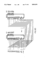
- FIGS. 1 and 2 are a system block diagram showing a preferred embodiment made according to the present invention.
- FIGS. 3 through 89 show the detailed schematics of the embodiment of FIGS. 1 and 2 organized into groups of components placed on five separate printed circuit boards in the preferred embodiment, and;
- FIGS. 90 through 95 show a preferred placement of the integrated circuits for FIGS. 3 through 89 on 5 expansion boards for use in conjunction with a host computer.
- Computer 100 includes a single 32-bit system data bus 101.
- An interface assembly 102 is coupled to bus 101 for interfacing with a host computer 103, which for the preferred embodiment is an IBM PC/AT, made by International Business Machines, Inc., or equivalent personal computer.
- Assembly 102 includes a bus interface transceiver 104, an 8-bit status register 105 for requesting host services, and an 8 bit service request register 106 for the host to request services of computer 100.
- the host interface adapter 107 provides the necessary 8 bit host to 32 bit computer data sizing changes. Hosts in other embodiments would not necessarily be restricted to an 8-bit interface.
- Memory stack means are provided in the form of a data stack 108 and a return address stack 109. Each stack is organized in the preferred embodiment as 4 kilowords of 32 bits per word. Each stack has an associated pointer. Specifically, a data stack pointer 110 is associated with data stack 108, and a return stack pointer 111 is associated with return stack 109. As can be seen, each stack pointer receives as input the low 12 bits from bus 101 and has its output connected to the address input of the corresponding stack, as well as through a transmitter 112 or 113 to bus 101. The data stack data inputs and outputs are buffered through transceiver 114 to provide for better current driving capability. The return stack data may be read from or written to the data bus 101 through the transceiver 116. In addition, the return stack data may be read from the address counter 117 or written to the address latch 118.
- the RAM address latch 118 and the next address register 119 are the two possible sources for the low 23 bits of address to the program memory (RAM) 121.
- the bits 23-30 of program memory address are provided by a page register 120, allowing up to 2 gigabytes of addressable program memory organized as a group of non-overlapping 8 megabyte pages.
- the next address register 119 is used to address memory 121.
- the contents of the address counter 117 are loaded with the address of the calling program, incremented by 4, and saved in the return stack 109 for use upon subroutine return.
- the return pointer 111 is decremented before writing to return stack 109.
- return stack 109 Upon subroutine return, return stack 109 provides an address through RAM address latch 118 to address program RAM 121.
- RAM address latch 118 retains the address while return stack pointer 111 is incremented to pop the return address off the return stack.
- the instruction fetched from program RAM 121 is stored in next address register 119 and the instruction latch 125 at the end of the fetching operation. Thus, each instruction directly addresses the next instruction through the next address register 119 and program RAM 121.
- the address counter 117 and next address register 119 are not used as a program counter in the conventional sense.
- the program counter is a hardware device used as the primary means of generating addresses for program memory whose normal operation is to increment in some manner while accessing sequential instructions.
- the next address register 119 is a simple holding register that is used to hold the address of the next instruction to be fetched from memory. The value of the next address register 119 is determined by an address field contained within the previous instruction executed, NOT from incrementing the previous register value.
- the address counter 117 is not directly involved in computing instruction addresses; it is only used to generate subroutine return addresses. Thus, computer 100 uses address information in each instruction to determine the address of the next instruction to be executed for high level language programs.
- Program RAM 121 is organized as a 32-bit program memory addressable for full-words only on evenly divisible by 4 byte addresses.
- Computer 100 provides a minimum quantity of 512 kilobytes of program memory, with expansion of up to 8 megabytes of program memory possible. A minor modification of the memory expansion boards, employed to allow for decoding more boards, allows use of up to 2 gigabytes of program memory.
- Program memory words of 32 bits are read from or written to the data bus 101 through transceiver 123. Additionally, single byte values with the high 24 bits set to 0 may be read and written to any byte (within each 32-bit word) in memory through the byte addressing and data routing block 122.
- the thirty-two bit arithmetic logic unit (ALU) 126 has its A input connected to a data high register (DHI) 127 and its B input connected to the data bus 101 through a transparent latch 128.
- the output of the ALU 126 is connected to a multiplexer 129 that provides for data pass-through, single bit shift left and shift right operations, and a byte rotate right operation.
- the output of ALU 126 is always fed back into the DHI register 127.
- the DHI register 127 is connected to data bus 101 through a data transmitter 130.
- a data low register (DLO) 131 is connected via a bidirectional path to the data bus 101, and its shift in/out signals are connected to the multiplexer 129 to provide a 64-bit shifting capability.
- the opcode portion of program RAM 121 is connected to instruction latch 125 for the purpose of holding the next opcode to be executed by the machine.
- This instruction latch 125 is decoded according to existing interrupt information from interrupt register 126 and conditional branching information from the condition code register 127 to form the contents of the micro-program counter 129.
- the micro-program counter 129 forms a 12 bit address into micro- program memory 131.
- the three low bits of the address into micro-program memory 131 are generated from a combination of the micro-address constant inputs and decoding of the condition select field to allow for conditional branching.
- the contents of the output of the decoding/address logic 128 and the micro-program counter 129 may be read to data bus 101 for diagnostic and interrupt processing purposes through bus driver 130.
- Micro-program memory 131 is a 32-bit high speed memory of 4 kilowords in length. Its data may be read or written to data bus 101 through transceiver 132, providing a writable instruction set capability. During program execution, its data is fed into the micro-instruction register 133 to provide control signals for operation. Micro-instruction register 133 may be read to data bus 101 through transmitter 134 for diagnostic purposes.
- FIGS. 3-89 The detailed schematics of the various integrated circuits forming computer 100 are shown in FIGS. 3-89. Narrative text preceding each group of figures gives descriptions of each signal mnemonic used in the schematics. Other than to identify general features of these circuits, they will not be described in detail, the detail being ascertainable from the hardware themselves. However, some general comments are in order.
- Computer 100 in its preferred embodiment is designed for construction on five boards which take five expansion slots in a personal computer. It is addressed with conventional 8088 microprocessor IN and OUT port instructions. It uses 32-bit data paths and 32- bit horizontal microcode (of which bits only 30 are actually used.) It operates on a jumper- and crystal-oscillator controlled micro-instruction cycle period which is preferably set at 150 ns. Most of the logic is the 74ALS series. The ALU is composed of eight 74F181 integrated circuits with carry-lookahead logic. Stack and microcode memory chips are 35 ns CMOS 4-bit chips. Program memory is 120 ns low power CMOS 8-bit memory chips.
- Variable benchmarks show speed increases of 5 to 10 times over an 80286 running at 8 MHz with zero-wait-state memory.
- An expert system benchmark shows an even more impressive performance of in excess of 640,000 logical inferences per second.
- Instruction decoding requires a 2-cycle minimum on a microcode word definition.
- FIGS. 3-14 describe the host interface adapter card (referred to as the "host" card.)
- the host card included in the preferred embodiment is suited for use in an IBM PC computer or compatible, but other functionally similar embodiments are possible for use with other host computers.
- FIG. 3 shows the host address bus decoding logic used to activate the board for operation during a host 103 IN or OUT port operation. Jumpers J1 through J14 are used to select the decoded address to any bank of eight ports in the port address space.
- FIG. 4 shows the decoders IC11 and IC12 which generate control signals based on the lowest bits of the port addresses. In common usage, the preferred embodiment uses eight output ports and three input ports as follows:
- FIG. 5 shows the generation of control signals and direct memory access (DMA) handshaking signals for the host interface.
- the host board is capable of accepting high-speed DMA transfers to or from host computer 103 memory directly to and from computer 100 memory.
- FIGS. 6-12 show the data paths for conversion between an 8-bit host 103 data bus and the 32-bit data bus 101, as well as the buffering for data and control signals on the ribbon cables connecting the host card to the interface card described next.
- FIGS. 13-14 show the connector arrangements for the host card to host computer bus connector and for the host card to interface card connectors.
- the Interface And Stack Card (called the interface card) described by FIGS. 15-40 performs a dual function: It serves as the control for bus transfers from the host card and within computer 100 over data bus 101, and provides both the data stack means 108 and the return stack means 109.
- FIGS. 15-16 show storage for bits 0-15 of the microcode memory and the micro-instruction register. The micro-instruction format is discussed in Appendix B.
- FIG. 17 shows the service request register IC58 which is used by the host computer 103 to request one of 255 possible programmable service types from the computer 100. Also shown is the status register IC57 which is used by computer 100 to signal a request for service from host computer 103.
- FIGS. 18-20 show data and control signal buffers between the host card and the interface card.
- FIGS. 21-22 show the clock generating circuits for computer 100. Jumpers J0 through J3 in FIG. 21, along with a socket to change the crystal oscillator used for OS0 allow selection of a wide range of oscillator frequencies. The preferred frequency for the preferred embodiment is 5.0 million Hertz.
- FIG. 22 shows that a fast clock FASTC is generated that is several nanoseconds ahead in phase of the system clock XCLK for the purpose of satisfying hold times of chips that require data to be valid after the clock rising edge.
- FIG. 23 shows the data bus 101 source and destination decoders. The devices in this figure generate signals to select only one device to drive data bus 101 and one device to receive data from bus 101.
- FIG. 24 shows miscellaneous control gates for microcode memory and the micro-instruction register.
- FIGS. 25-28 show the data stack means.
- the data stack has a 12-bit up/down counter that may be incremented, decremented, or loaded from data bus 101 at the end of every clock cycle.
- the use of fast static RAM chips for the stack memory itself allows the data stack 108 to be read or written and then the stack pointer 110 to be changed on each clock cycle.
- FIGS. 30-34 show the return stack means.
- the implementation of the return stack 109 and return stack pointer 111 is very similar to that of the data stack 108 and data stack pointer 110.
- FIGS. 35-40 show connector arrangements for transmitting and receiving signals from other cards in the system and from the host adapter card.
- the Data, Arithmetic, and Logic Card The Data, Arithmetic, and Logic Card.
- the data, arithmetic and logic card (called the data card) described by FIGS. 41-53 performs all arithmetic and logical manipulation of data for computer 100.
- FIG. 41 shows storage for bits 16-23 of the microcode memory and the micro-instruction register. The micro-instruction format is discussed in Appendix B.
- FIGS. 42A-46 show the arithmetic and logic unit (ALU) 126, bus latch 128, data hi register 127, DHI to data bus 100 driver 130, and ALU multiplexer 129. Data from the DHI register 127 and/or the bus data latch 128 flows through the ALU 126 and multiplexer 129 on each clock cycle, then is written back to the DHI register 127.
- FIG. 47 shows the DLO register 131.
- FIG. 48 shows the logic used to detect when the output of the ALU is exactly zero. This is very useful for conditional branching.
- FIG. 49 shows the generation of the data bus latch 128 control signal and the shift-in bits to the DLO register 131 and the DHI register 127. These shift-in bits are conditioned to provide capability of one-cycle-per-bit multiplication shift-and-conditional-add and non-restoring division algorithms.
- FIG. 50 shows the conditioning of ALU 126 input control signals to likewise provide for efficient multiplication and division functions.
- FIGS. 51-53 show connector arrangements for transmitting and receiving signals from other cards in the system.
- FIG. 54 shows storage for bits 24-31 of the microcode memory and the micro-instruction register.
- the micro-instruction format is discussed in Appendix B.
- FIG. 55 shows the arrangement of the RAM address latch 118.
- the RAM address latch is used to address program memory for all non-instruction operations, for return from subroutine operations, and passes data through for DMA transfers with host 103.
- FIGS. 56-58 show the address counter 117. The address counter 117 may be incremented and passed through the address latch 118 to step through memory one word at a time during DMA access or block memory operations. The address counter 117 is also incremented when performing a subroutine call operation in order to save a correct subroutine return address in return stack 109.
- FIG. 59 shows the next address register 119 and page register 120. The next address register is used to store the address field of an instruction that points to the memory address of the next instruction during the instruction fetch and decode operation.
- FIG. 60 shows the logic used to control return stack 109 and return stack pointer 111. In particular, this logic implements the subroutine call and return control operations for the return stack means.
- FIG. 61 shows the instruction latch 125 and micro-program counter 129.
- FIG. 62 shows the interrupt status register 126. Interrupts are set by a processor condition pulling a "PR" pin of IC53-IC56 low, causing the flip-flop to activate, or by loading a one bit from data bus 101. Any one or more active interrupts causes an interrupt at the next instruction decoding operation. An interrupt mask bit from IC53 pin 5 is used to allow masking of all further interrupts during interrupt processing.
- FIG. 63 shows the condition code register 127. This register is set at the end of every clock cycle, and forms the basis of the lowest bit of the next micro-instruction address fetched during the succeeding clock cycle.
- FIG. 64 shows a special forcing driver for the microcode-memory address that forces an opcode of 1 during interrupt recognition.
- FIG. 65 shows a timing chain used to control the 2 cycle instruction fetch and decoding operation.
- FIGS. 66-69 show the RAM data to data bus 101 transfer logic shown by block 122 on FIG. 1. This transfer logic allows access of arbitrary bytes within the 32-bit memory organization as well as 32-bit full word access on evenly-divisible-by-four memory address locations.
- FIGS. 70-75 show connector arrangements for transmitting and receiving signals from other cards in the system.
- the Memory Card The memory card described by FIGS. 76-89 is a single program memory 121 storage card for computer 100. Computer 100 may have one to sixteen of these cards in operation simultaneously to use up to 8 megabytes of memory.
- FIG. 76 shows data buffering logic used to satisfy current driving requirements of the memory chips.
- FIG. 77 shows address buffering logic.
- FIG. 78 shows the memory board selection, bank selection, and chip selection logic. Jumpers J0-J7 may be set to map the memory board to one of 16 non-overlapping 512 kilobyte locations within the first eight megabytes of the available memory space. Only one memory board is activated at a time. Once the memory board is activated, a particular bank of chips (numbered from 0-3) is enabled selecting a 32 kiloword address within the board. If byte memory access is being used, a single chip within the bank is selected for a single byte operation, otherwise all chips within the bank are enabled.
- FIGS. 79-86 show the four banks of four RAM chips each.
- FIGS. 87-89 show connector arrangements for transmitting and receiving signals from other cards in the system.
- Computer 100 in this preferred embodiment uses various software packages, including a FORTH kernel, a cross-compiler, a micro-assembler, as well as microcode.
- the software for these packages, written using MVP-FORTH, are listed in Appendix A. Further, the microcode format is discussed in Appendix B.
- the User's Manual (less appendices duplicated elsewhere in this document) is included as Appendix C. Some general comments about the software are in order.
- the Cross-Compiler The cross-compiler maintains a sealed vocabulary with all the words currently defined for computer 100. At the base of this dictionary are special cross-compiler words such as IF ELSE THEN : and ;.
- words are added to this sealed vocabulary and are also cross-compiled into computer 100.
- keyword CROSS-COMPILER any word definitions, constants, variables, etc. will be compiled to computer 100.
- any immediate operations will be taken from the cross-compiler's vocabulary, which is chained to the normal MVP-FORTH vocabulary.
- the cross-compiler By entering the FORTH word ⁇ , the cross-compiler enters the immediate execution mode for computer 100. All words are searched for in the sealed vocabulary for computer 100 and are executed by computer 100 itself. The "START..” "END" that is displayed indicates the start and the end of execution of computer 100. If the execution freezes in between the start and end, that means that computer 100 is hung up. The cross-compiler builds a special FORTH word in computer 100 to execute the desired definition, then performs a HALT instruction. Entering the FORTH word ⁇ will leave the computer 100 mode of execution and return to the cross-compiler. No colon definitions or other creation of dictionary entries should be performed while between ⁇ and ⁇ .
- the FORTH word CPU32 will automatically transfer control of the system to computer 100 via its Forth language cold start command.
- the host MVP-FORTH will then execute an idle loop waiting for computer 100 to request services.
- the word BYE will return control back the host's MVP FORTH.
- the current cross-compiler can not keep track of the dictionary pointer DP, etc., in computer 100 if it is out of sync with the cross-compiler's copy. This means that no cross- C compiling or micro-assembly may be done after the FORTH of computer 100 has altered the dictionary in any way. This could be fixed at a later date by updating the cross-compiler's variables from computer 100 after every BYE command of computer 100.
- the Micro-assembler is a tool to save the programmer from having to set all the bits for microcode by hand. It allows the use of mnemonics for setting the micro-operation fields in a micro-instruction, and, for the most part, automatically handles the micro-instruction addressing scheme.
- the micro-assembler is written to be co-resident with the cross-compiler. It uses the same routines for computer 100 and sealed host vocabulary dictionary handling, etc. Currently all microcode must be defined before the board starts altering its dictionary, but this could be changed as discussed previously.
- a micro-instruction is a 32-bit instruction in microcode, while a micro-operation is formed by one or more microcode fields within a single micro-instruction.
- Appendix B gives a quick reference to all the hardware-defined micro-instruction fields supported by the micro-assembler.
- the usage and operation of each field of the micro-instruction format is covered in detail in Part Two of the User's Manual included as Appendix C.
- the microcode layout is very horizontal, there is a direct relationship between bit settings and control line inputs to various chips on computer 100. As with most horizontally microcoded machines, as many micro-operations as desired may take place at the same time, although some operations don't do anything useful when used together.
- Microcode Definitions Format The micro-assembler has a few keywords to make life easier for the micro-programmer.
- the word OP-CODE starts a microcode definition.
- the input parameter is the page number from 0-OFF hex that the op-code resides in.
- the word ⁇ is op-code 7. This means that whenever computer 100 interprets a hex 038xxxxx (where the x's represent don't care bit values), the word ⁇ will be executed in microcode.
- the character string after OP-CODE: is the name of the op-code that will be added to the cross-compiler and computer 100 dictionaries. It is the programmer's responsibility to ensure that two op-codes are not assigned to the same microcode memory page.
- the variable CURRENT-OPCODE contains the page currently assigned by OP-CODE:. It may be changed to facilitate multi-page definitions.
- the word :: signifies the start of the definition of a micro-instruction.
- the number before :: must be from 0 to 7, and signifies the offset from 0 to 7 within the current micro-program memory page for that micro-instruction.
- Micro-instructions may be defined in any order desired.
- the word >> may be used without a preceding number instead of the sequence 0 ::.
- the word ;; signifies the end of a micro-instruction and stores the micro-instruction into the appropriate location in micro-program memory.
- ;;END signifies the end of a definition of a FORTH microcoded primitive.
- the programmer may single-step microcoded programs. Use the >> word to start a micro-instruction. Instead of using ;;, use ;SET to copy the micro-instruction to the MIR. This allows reading resources of computer 100 to the host 103 with the X@ word or storing resource values with the X- word. Using ;DO instead of ;; will load the instruction into the MIR and cycle the clock once. This is an excellent way of single-stepping microcode.
- the User's Manual in Appendix C and the Diagnostics of computer 100 given in Appendix A part III provide examples of how to use these features. End/Decode.
- END and DECODE are the two micro-operations that perform the FORTH NEXT function and perform subroutine calls, subroutine returns, and unconditional branches in parallel with other operations.
- DECODE is always in the next to last micro-instruction of a microcoded instruction. It causes the interrupt register 126 to be clocked near the falling clock edge, and loads highest 9 bits of the instruction into the instruction latch 125 at the following rising clock edge. Thereafter, instruction fetching and decoding proceeds according to the actions described in Appendix C part II.
- END is a micro-operation that marks the last instruction in a program and forces a jump to offset 0 of the next instruction's microcoded memory page. Microcode Next Address Generation.
- a conditional jump allows jumping to one of the two locations depending on the value of one of the 8 condition codes.
- the unconditional jump described in the preceding paragraph is just a special conditional jump in which the condition picked is a constant that is always set to 0 or 1.
- the sign bit conditional jump is used below as an example.
- a conditional jump sets the lowest bit of the next micro-instruction address to the value of the condition that was valid at the end of the previous microcycle.
- the first two bits are always numeric, indicating the top two binary bits of the jump destination address within the micro-program memory page.
- Appendix C is the user manual for computer 100, and describes other information of interest in the operation of the preferred embodiment of the invention.
Landscapes
- Engineering & Computer Science (AREA)
- Software Systems (AREA)
- Theoretical Computer Science (AREA)
- Physics & Mathematics (AREA)
- General Engineering & Computer Science (AREA)
- General Physics & Mathematics (AREA)
- Executing Machine-Instructions (AREA)
Abstract
Description
______________________________________
FIGURE  FILE      DESCRIPTION
NUMBER  NAME      OF CONTENTS
______________________________________
SYSTEM BLOCK DIAGRAM
 1      SBLOCK    ALU AND MEMORY AD-
                  DRESS BLOCK DIAGRAM
 2      MBLOCK    INSTRUCTION DECOD-
                  ING AND HOST INTERFACE
                  BLOCK DIAGRAM
HOST ADAPTER BOARD
 3      HOST1     HOST ADDRESS DECODER
 4      HOST2     READ/WRITE DECODER
 5      HOST3     DMA CONTROL LOGIC
 6      HOST4     DATA WIDTH CONVERTER
                  FROM HOST
 7      HOST5     DATA WIDTH CONVERTER TO
                  HOST
 8      HOST6     DATA WIDTH CONVERTER
                  CONTROL LOGIC
 9      HOST7     HOST DATA BUS BUFFER
10      HOST8     CONTROL SIGNAL TRANS-
                  MITTER - 1
11      HOST9     32-BIT DATA SIGNAL BUS
                  TERMINATORS
12      HOST10    CONTROL SIGNAL
                  TRANSMITTER - 2
13      CON1      HOST EDGE CONNECTOR
14      CON3      HOST TO CPU/32 RIBBON
                  CABLES
The signal descriptions for the host adapter (HOST) board are -listed in
Appendix D on  pages  1 and 2.
HOST INTERFACE & STACK MEMORY BOARD
15      MRAM1     MICRO-PROGRAM (0-7)
16      MRAM2     MICRO-PROGRAM (8-15)
17      INT1      STATUS & SERVICE REQUEST
                  REGS
18      INT2      DATA BUFFER TO/FROM HOST
19      INT3      CONTROL SIGNAL SIGNAL
                  BUFFER - 1
20      INT4      CONTROL SIGNAL BUFFER - 2
21      MISC1     SYSTEM CLOCK
                  GENERATOR/OSCILLATOR
22      MISC2     CLOCK CONDITIONING
23      MISC3     BUS SOURCE & DEST DECODERS
24      MISC4     MRAM CONTROL LOGIC
25      STACK1    DATA STACK POINTER
26      STACK2    DATA STACK RAM (0-7)
27      STACK3    DATA STACK RAM (8-15)
28      STACK4    DATA STACK RAM (16-23)
29      STACK5    DATA STACK RAM (24-31)
30      STACK6    RETURN STACK POINTER
31      STACK7    RETURN STACK RAM (0-7)
32      STACK8    RETURN STACK RAM (8-15)
33      STACK9    RETURN STACK RAM (16-23)
34      STAK10    RETURN STACK RAM (24-31)
35      CON2      DATA & CONTROL BUS RIBBON
                  CABLES
36      CON3      HOST TO CPU/32 RIBBON
                  CABLES
37      CON4      DATA TO INTERFACE
                  BOARD RIBBON CABLE
38      CON5      INTERFACE TO ADDRESS
                  BOARD RIBBON CABLE "A"
39      CON6      INTERFACE TO ADDRESS
                  BOARD RIBBON CABLE "B"
40      CON9      PC-BUS POWER/GND
The signal descriptions for the host interface and stack
memory (INT) board are listed in Appendix D on pages 3-6.
ALU & DATA PATH BOARD
41      MRAM3     MICRO-PROGRAM BITS (16-23)
42A, 42B
        DATA1     ALU (0-7)
43A, 43B
        DATA2     ALU (8-15)
44A, 44B
        DATA3     ALU (16-23)
45A, 45B
        DATA4     ALU (24-31)
46      DATA5     ALU CARRY-LOOKAHEAD
47      DATA6     DLO REGISTER
48      DATA7     ALU ZERO DETECT
49      DATA8     SHIFT INPUT CONDITIONING
50      DATA9     ALU FUNCTION CONDITIONING
                  FOR DIVISION
51      CON2      DATA & CONTROL BUS RIBBON
                  CABLES
52      CON4      DATA TO INTERFACE BOARD
                  RIBBON CABLE
53      CON9      PC-BUS POWER/GND
The signal descriptions for the ALU and data path (DATA)
board are listed in Appendix D on pages 7-9.
MEMORY ADDRESS & MICROCODE CONTROL BOARD
54      MRAM4     MICRO-PROGRAM BITS (24-31)
        ADDR1     intentionally omitted
        ADDR2     intentionally omitted
55      ADDR3     RAM ADDRESS LATCH
56      ADDR4     ADDRESS COUNTER (2-9)
57      ADDR5     ADDRESS COUNTER (10-17)
58      ADDR6     ADDRESS COUNTER (18-31) & (0-1)
59      ADDR7     NEXT ADDRESS & PAGE
                  REGISTERS
60      ADDR8     RETURN STACK CONTROL
                  LOGIC
61      CONT1     INSTRUCTION REGISTER &
                  MICRO-PROGRAM COUNTER
62      CONT2     INTERUPT FLAG REGISTER
63      CONT3     CONDITION CODE REGISTER
64      CONT4     INTERRUPT MICRO-ADDRESS
                  REGISTER
65      CONT5     MISC CONTROL LOGIC
66      RAM1      RAM DATA TO BUS INTERFACE
                  (0-7)
67      RAM2      RAM DATA TO BUS INTERFACE
                  (8-15)
68      RAM3      RAM DATA TO BUS INTERFACE
                  (16-23)
69      RAM4      RAM DATA TO BUS INTERFACE
                  (24-31)
70      CON2      DATA & CONTROL BUS RIBBON
                  CABLES
71      CON5      INTERFACE TO ADDRESS
                  BOARD RIBBON CABLE "A"
72      CON6      INTERFACE TO ADDRESS
                  BOARD RIBBON CABLE "B"
73      CON7      ADDRESS TO RAM BOARDS
                  RIBBON CABLE "A"
74      CON8      ADDRESS TO RAM BOARDS
                  RIBBON CABLE "B"
75      CON9      PC-BUS POWER/GND
The signal instructions for the memory address and microcode
control (ADDR) board are listed in Appendix D on pages 10-13.
MEMORY BOARD
(Note that up to sixteen memory boards may be used within
one system)
76      MEM1      RAM DATA BUFFER
77      MEM2      RAM ADDRESS BUFFER
78      MEM3      READ/WRITE/OUTPUT
                  CONTROL LOGIC
79      MEM4      RAM BANK 0 BITS (0-15)
80      MEM5      RAM BANK 0 BITS (16-31)
81      MEM6      RAM BANK 1 BITS (0- 15)
82      MEM7      RAM BANK 1 BITS (16-31)
83      MEM8      RAM BANK 2 BITS (0-15)
84      MEM9      RAM BANK 2 BITS (16-31)
85      MEM10     RAM BANK 3 BITS (0-15)
86      MEM11     RAM BANK 3 BITS (16-31)
87      CON7      ADDR TO MEMORY BOARD
                  RIBBON CABLE "A"
88      CON8      ADDR TO MEMORY BOARD
                  RIBBON CABLE "B"
89      CON9      PC-BUS POWER/GND
The signal instructions for the memory (MEM) board are listed
in Appendix D on page 14.
______________________________________
______________________________________
PORT   FUNCTION
______________________________________
OUTPUT
300    DATA BUS (AUTOMATICALLY SEQUENCED
       FOR 4 BYTES)
301    MIR (WRITE 4 TIMES JUST LIKE WRITE0)
302    SINGLE STEP BOARD CLOCK
303    START BOARD
304    STOP BOARD
305    SET DMA MODE
306    RESET DATA BUS SEQUENCER & DMA MODE
307    SERVICE REQUEST REG & INTERUPT
INPUT
300    DATA BUS (AUTOMATICALLY SEQUENCED
       FOR 4 BYTES)
301    MIR (READ 4 TIMES JUST LIKE READ0)
302    STATUS REGISTER (8 BITS)
______________________________________
Claims (9)
Priority Applications (1)
| Application Number | Priority Date | Filing Date | Title |
|---|---|---|---|
| US07/058,737 US5053952A (en) | 1987-06-05 | 1987-06-05 | Stack-memory-based writable instruction set computer having a single data bus |
Applications Claiming Priority (1)
| Application Number | Priority Date | Filing Date | Title |
|---|---|---|---|
| US07/058,737 US5053952A (en) | 1987-06-05 | 1987-06-05 | Stack-memory-based writable instruction set computer having a single data bus |
Publications (1)
| Publication Number | Publication Date |
|---|---|
| US5053952A true US5053952A (en) | 1991-10-01 |
Family
ID=22018628
Family Applications (1)
| Application Number | Title | Priority Date | Filing Date |
|---|---|---|---|
| US07/058,737 Expired - Fee Related US5053952A (en) | 1987-06-05 | 1987-06-05 | Stack-memory-based writable instruction set computer having a single data bus |
Country Status (1)
| Country | Link |
|---|---|
| US (1) | US5053952A (en) |
Cited By (40)
| Publication number | Priority date | Publication date | Assignee | Title |
|---|---|---|---|---|
| US20010012975A1 (en) * | 1999-12-15 | 2001-08-09 | Naoto Matsumoto | System for rewriting control program in vending machine |
| US20030212878A1 (en) * | 2002-05-07 | 2003-11-13 | Chen-Hanson Ting | Scaleable microprocessor architecture |
| US7032100B1 (en) | 1999-12-17 | 2006-04-18 | Koninklijke Philips Electronics N.V. | Simple algorithmic cryptography engine |
| US20070192576A1 (en) * | 2006-02-16 | 2007-08-16 | Moore Charles H | Circular register arrays of a computer |
| US20080270648A1 (en) * | 2007-04-27 | 2008-10-30 | Technology Properties Limited | System and method for multi-port read and write operations |
| US20100023730A1 (en) * | 2008-07-24 | 2010-01-28 | Vns Portfolio Llc | Circular Register Arrays of a Computer |
| US7904615B2 (en) | 2006-02-16 | 2011-03-08 | Vns Portfolio Llc | Asynchronous computer communication |
| US7937557B2 (en) | 2004-03-16 | 2011-05-03 | Vns Portfolio Llc | System and method for intercommunication between computers in an array |
| US7941641B1 (en) | 2007-10-01 | 2011-05-10 | Yong-Kyu Jung | Retargetable instruction decoder for a computer processor |
| US7966481B2 (en) | 2006-02-16 | 2011-06-21 | Vns Portfolio Llc | Computer system and method for executing port communications without interrupting the receiving computer |
| US20120216022A1 (en) * | 2010-06-23 | 2012-08-23 | International Business Machines Corporation | Controlling the selectively setting of operational parameters for an adapter |
| US8468284B2 (en) | 2010-06-23 | 2013-06-18 | International Business Machines Corporation | Converting a message signaled interruption into an I/O adapter event notification to a guest operating system |
| US8478922B2 (en) | 2010-06-23 | 2013-07-02 | International Business Machines Corporation | Controlling a rate at which adapter interruption requests are processed |
| US8504754B2 (en) | 2010-06-23 | 2013-08-06 | International Business Machines Corporation | Identification of types of sources of adapter interruptions |
| US8505032B2 (en) | 2010-06-23 | 2013-08-06 | International Business Machines Corporation | Operating system notification of actions to be taken responsive to adapter events |
| US8510599B2 (en) | 2010-06-23 | 2013-08-13 | International Business Machines Corporation | Managing processing associated with hardware events |
| US8549182B2 (en) | 2010-06-23 | 2013-10-01 | International Business Machines Corporation | Store/store block instructions for communicating with adapters |
| US8566480B2 (en) | 2010-06-23 | 2013-10-22 | International Business Machines Corporation | Load instruction for communicating with adapters |
| US8572635B2 (en) | 2010-06-23 | 2013-10-29 | International Business Machines Corporation | Converting a message signaled interruption into an I/O adapter event notification |
| US8621112B2 (en) | 2010-06-23 | 2013-12-31 | International Business Machines Corporation | Discovery by operating system of information relating to adapter functions accessible to the operating system |
| US8626970B2 (en) | 2010-06-23 | 2014-01-07 | International Business Machines Corporation | Controlling access by a configuration to an adapter function |
| US8631222B2 (en) | 2010-06-23 | 2014-01-14 | International Business Machines Corporation | Translation of input/output addresses to memory addresses |
| US8639858B2 (en) | 2010-06-23 | 2014-01-28 | International Business Machines Corporation | Resizing address spaces concurrent to accessing the address spaces |
| US8650335B2 (en) | 2010-06-23 | 2014-02-11 | International Business Machines Corporation | Measurement facility for adapter functions |
| US8650337B2 (en) | 2010-06-23 | 2014-02-11 | International Business Machines Corporation | Runtime determination of translation formats for adapter functions |
| WO2014151691A1 (en) * | 2013-03-15 | 2014-09-25 | Soft Machines, Inc. | Method and apparatus for guest return address stack emulation supporting speculation |
| US9032375B2 (en) | 2011-04-27 | 2015-05-12 | International Business Machines Corporation | Performance bottleneck identification tool |
| US9195623B2 (en) | 2010-06-23 | 2015-11-24 | International Business Machines Corporation | Multiple address spaces per adapter with address translation |
| US9213661B2 (en) | 2010-06-23 | 2015-12-15 | International Business Machines Corporation | Enable/disable adapters of a computing environment |
| US9436476B2 (en) | 2013-03-15 | 2016-09-06 | Soft Machines Inc. | Method and apparatus for sorting elements in hardware structures |
| US9582322B2 (en) | 2013-03-15 | 2017-02-28 | Soft Machines Inc. | Method and apparatus to avoid deadlock during instruction scheduling using dynamic port remapping |
| US9627038B2 (en) | 2013-03-15 | 2017-04-18 | Intel Corporation | Multiport memory cell having improved density area |
| US9710387B2 (en) | 2011-01-27 | 2017-07-18 | Intel Corporation | Guest instruction to native instruction range based mapping using a conversion look aside buffer of a processor |
| US9891915B2 (en) | 2013-03-15 | 2018-02-13 | Intel Corporation | Method and apparatus to increase the speed of the load access and data return speed path using early lower address bits |
| US9921842B2 (en) | 2011-01-27 | 2018-03-20 | Intel Corporation | Guest instruction block with near branching and far branching sequence construction to native instruction block |
| US9946538B2 (en) | 2014-05-12 | 2018-04-17 | Intel Corporation | Method and apparatus for providing hardware support for self-modifying code |
| US10185567B2 (en) | 2011-01-27 | 2019-01-22 | Intel Corporation | Multilevel conversion table cache for translating guest instructions to native instructions |
| US10241795B2 (en) | 2011-01-27 | 2019-03-26 | Intel Corporation | Guest to native block address mappings and management of native code storage |
| US10394563B2 (en) | 2011-01-27 | 2019-08-27 | Intel Corporation | Hardware accelerated conversion system using pattern matching |
| US10514926B2 (en) | 2013-03-15 | 2019-12-24 | Intel Corporation | Method and apparatus to allow early dependency resolution and data forwarding in a microprocessor |
Citations (19)
| Publication number | Priority date | Publication date | Assignee | Title |
|---|---|---|---|---|
| US3215987A (en) * | 1962-06-04 | 1965-11-02 | Sylvania Electric Prod | Electronic data processing |
| US3629857A (en) * | 1969-09-18 | 1971-12-21 | Burroughs Corp | Computer input buffer memory including first in-first out and first in-last out modes |
| US3757306A (en) * | 1971-08-31 | 1973-09-04 | Texas Instruments Inc | Computing systems cpu |
| US3771141A (en) * | 1971-11-08 | 1973-11-06 | Culler Harrison Inc | Data processor with parallel operations per instruction |
| US3786432A (en) * | 1972-06-20 | 1974-01-15 | Honeywell Inf Systems | Push-pop memory stack having reach down mode and improved means for processing double-word items |
| US4045781A (en) * | 1976-02-13 | 1977-08-30 | Digital Equipment Corporation | Memory module with selectable byte addressing for digital data processing system |
| US4204252A (en) * | 1978-03-03 | 1980-05-20 | Digital Equipment Corporation | Writeable control store for use in a data processing system |
| US4210960A (en) * | 1977-09-02 | 1980-07-01 | Sperry Corporation | Digital computer with overlapped operation utilizing conditional control to minimize time losses |
| US4415969A (en) * | 1980-02-07 | 1983-11-15 | Intel Corporation | Macroinstruction translator unit for use in a microprocessor |
| US4447875A (en) * | 1981-07-07 | 1984-05-08 | Burroughs Corporation | Reduction processor for executing programs stored as treelike graphs employing variable-free applicative language codes |
| US4491912A (en) * | 1981-03-18 | 1985-01-01 | Hitachi, Ltd. | Data processing system with improved microsubroutine facility |
| US4546431A (en) * | 1982-11-03 | 1985-10-08 | Burroughs Corporation | Multiple control stores in a pipelined microcontroller for handling jump and return subroutines |
| US4615003A (en) * | 1984-06-05 | 1986-09-30 | Burroughs Corporation | Condition concentrator and control store for a reduction processor evaluating programs stored as binary directed graphs employing variable-free applicative language codes |
| US4618925A (en) * | 1981-05-22 | 1986-10-21 | Data General Corporation | Digital data processing system capable of executing a plurality of internal language dialects |
| US4654780A (en) * | 1984-06-05 | 1987-03-31 | Burroughs Corporation | Parallel register transfer mechanism for a reduction processor evaluating programs stored as binary directed graphs employing variable-free applicative language codes |
| US4674032A (en) * | 1984-04-02 | 1987-06-16 | Unisys Corporation | High-performance pipelined stack with over-write protection |
| US4719565A (en) * | 1984-11-01 | 1988-01-12 | Advanced Micro Devices, Inc. | Interrupt and trap handling in microprogram sequencer |
| US4791551A (en) * | 1985-02-11 | 1988-12-13 | Analog Devices, Inc. | Microprogrammable devices using transparent latch |
| US4835738A (en) * | 1986-03-31 | 1989-05-30 | Texas Instruments Incorporated | Register stack for a bit slice processor microsequencer |
-
1987
- 1987-06-05 US US07/058,737 patent/US5053952A/en not_active Expired - Fee Related
Patent Citations (19)
| Publication number | Priority date | Publication date | Assignee | Title |
|---|---|---|---|---|
| US3215987A (en) * | 1962-06-04 | 1965-11-02 | Sylvania Electric Prod | Electronic data processing |
| US3629857A (en) * | 1969-09-18 | 1971-12-21 | Burroughs Corp | Computer input buffer memory including first in-first out and first in-last out modes |
| US3757306A (en) * | 1971-08-31 | 1973-09-04 | Texas Instruments Inc | Computing systems cpu |
| US3771141A (en) * | 1971-11-08 | 1973-11-06 | Culler Harrison Inc | Data processor with parallel operations per instruction |
| US3786432A (en) * | 1972-06-20 | 1974-01-15 | Honeywell Inf Systems | Push-pop memory stack having reach down mode and improved means for processing double-word items |
| US4045781A (en) * | 1976-02-13 | 1977-08-30 | Digital Equipment Corporation | Memory module with selectable byte addressing for digital data processing system |
| US4210960A (en) * | 1977-09-02 | 1980-07-01 | Sperry Corporation | Digital computer with overlapped operation utilizing conditional control to minimize time losses |
| US4204252A (en) * | 1978-03-03 | 1980-05-20 | Digital Equipment Corporation | Writeable control store for use in a data processing system |
| US4415969A (en) * | 1980-02-07 | 1983-11-15 | Intel Corporation | Macroinstruction translator unit for use in a microprocessor |
| US4491912A (en) * | 1981-03-18 | 1985-01-01 | Hitachi, Ltd. | Data processing system with improved microsubroutine facility |
| US4618925A (en) * | 1981-05-22 | 1986-10-21 | Data General Corporation | Digital data processing system capable of executing a plurality of internal language dialects |
| US4447875A (en) * | 1981-07-07 | 1984-05-08 | Burroughs Corporation | Reduction processor for executing programs stored as treelike graphs employing variable-free applicative language codes |
| US4546431A (en) * | 1982-11-03 | 1985-10-08 | Burroughs Corporation | Multiple control stores in a pipelined microcontroller for handling jump and return subroutines |
| US4674032A (en) * | 1984-04-02 | 1987-06-16 | Unisys Corporation | High-performance pipelined stack with over-write protection |
| US4615003A (en) * | 1984-06-05 | 1986-09-30 | Burroughs Corporation | Condition concentrator and control store for a reduction processor evaluating programs stored as binary directed graphs employing variable-free applicative language codes |
| US4654780A (en) * | 1984-06-05 | 1987-03-31 | Burroughs Corporation | Parallel register transfer mechanism for a reduction processor evaluating programs stored as binary directed graphs employing variable-free applicative language codes |
| US4719565A (en) * | 1984-11-01 | 1988-01-12 | Advanced Micro Devices, Inc. | Interrupt and trap handling in microprogram sequencer |
| US4791551A (en) * | 1985-02-11 | 1988-12-13 | Analog Devices, Inc. | Microprogrammable devices using transparent latch |
| US4835738A (en) * | 1986-03-31 | 1989-05-30 | Texas Instruments Incorporated | Register stack for a bit slice processor microsequencer |
Non-Patent Citations (46)
| Title |
|---|
| "Stack-Oriented WISC Machine", WISC Technologies, La Honda, Ca., 94020, 2 pages. |
| A. C. D. Haley, "The KDF.9 Computer System", AFIPS Conference Proceedings, vol. 22, 1962 Fall Joint Computer Conference, pp. 108-120. |
| A. C. D. Haley, The KDF.9 Computer System , AFIPS Conference Proceedings, vol. 22, 1962 Fall Joint Computer Conference, pp. 108 120. * |
| BYTE 6/86, Microcoded IBM PC Board, Mtn. Vw. Press Advertisement, Haydon, MVP Microcoded CPU/16, Mountain View Press, 4 pages. * |
| Castan et al., 3L: An HLL RISC Processor for Parallel Execution of FP Language Programs, Symposium on Core Computer Architecture, 9, pp. 239 247, 1982. * |
| Castan et al., μ3L: An HLL-RISC Processor for Parallel Execution of FP Language Programs, Symposium on Core Computer Architecture, #9, pp. 239-247, 1982. |
| Ditzel and McLellan, "Branch Folding in the CRISP Microprocessor: Reducing Branch Delay to Zero", ACM, 6/2/87, pp. 2-9. |
| Ditzel and McLellan, Branch Folding in the CRISP Microprocessor: Reducing Branch Delay to Zero , ACM, 6/2/87, pp. 2 9. * |
| Ditzel, McLellan and Berenbaum, "The Hardware Architecture of the CRISP Microprocessor", ACM, 6/2/87, pp. 309-319. |
| Ditzel, McLellan and Berenbaum, The Hardware Architecture of the CRISP Microprocessor , ACM, 6/2/87, pp. 309 319. * |
| Folger et al., Computer Architectures Designing for Speed, Intellectual Leverage for the Information Society, Spring 83, pp. 25 31. * |
| Folger et al., Computer Architectures-Designing for Speed, Intellectual Leverage for the Information Society, Spring 83, pp. 25-31. |
| Grewe and Dixon, "A Forth Machine for the S-100 System", The Journal of Forth Application and Research, vol. 2, No. 1, 1984, pp. 23-32. |
| Grewe and Dixon, A Forth Machine for the S 100 System , The Journal of Forth Application and Research, vol. 2, No. 1, 1984, pp. 23 32. * |
| Haydon, A Unification of Software and Hardware; A New Tool for Human Thought, 1987 Rochester, Forth Conference, pp. 25 28. * |
| Haydon, A Unification of Software and Hardware; A New Tool for Human Thought, 1987 Rochester, Forth Conference, pp. 25-28. |
| Haydon, The Multi Dimensions of Forth, Forth Dimensions, vol. 8, No. 3, pp. 32 34, Sep./Oct., 1986. * |
| Haydon, The Multi-Dimensions of Forth, Forth Dimensions, vol. 8, No. 3, pp. 32-34, Sep./Oct., 1986. |
| Kaneda, Wada and Maekawa, "High-Speed Execution of Forth and Pascal Programs on a High-Level Language Machine", 1983, pp. 259-266. |
| Kaneda, Wada and Maekawa, High Speed Execution of Forth and Pascal Programs on a High Level Language Machine , 1983, pp. 259 266. * |
| Koopman & Haydon, MVP Microcoded CPU/16 Architecture, Mountain View Press, 4 pages. * |
| Koopman, Microcoded Versus Hard Wired Control, BYTE, Jan. 1987, pp. 235 242. * |
| Koopman, Microcoded Versus Hard-Wired Control, BYTE, Jan. 1987, pp. 235-242. |
| Koopman, The WISC Concept, BYTE, pp. 187 193, Apr. 1987. * |
| Koopman, The WISC Concept, BYTE, pp. 187-193, Apr. 1987. |
| Koopman, Writable Instruction Set, Stack Oriented Computers: The WISC Concept, 1987 Rochester Forth Conference, pp. 29 51. * |
| Koopman, Writable Instruction Set, Stack Oriented Computers: The WISC Concept, 1987 Rochester Forth Conference, pp. 29-51. |
| Larus, A Comparison of Microcode, Assembly Code & High Level Langauges on the VAX 11 & RISC I, Computer Architecture News, vol. 10, No. 5, pp. 10 15. * |
| Larus, A Comparison of Microcode, Assembly Code & High-Level Langauges on the VAX-11 & RISC I, Computer Architecture News, vol. 10, No. 5, pp. 10-15. |
| Norton & Abraham, Adaptive Interpretation as a Means of Exploiting Complex Instruction Sets, IEEE International Symposium on Computer Architecture, pp. 277 282, 1983. * |
| Norton & Abraham, Adaptive Interpretation as a Means of Exploiting Complex Instruction Sets, IEEE International Symposium on Computer Architecture, pp. 277-282, 1983. |
| Patterson et al., RISC Assessment: A High Level Language Experiment, Symposium on Computer Architecture, No. 9, pp. 3 8, 1982. * |
| Patterson et al., RISC Assessment: A High-Level Language Experiment, Symposium on Computer Architecture, No. 9, pp. 3-8, 1982. |
| Philip J. Koopman, Jr., Stack Computers The New Wave, 1989. * |
| Philip J. Koopman, Jr., Stack Computers-The New Wave, 1989. |
| Rust, ACTION Processor Forth Right, Rochester Forth Standards Conference, pp. 309 315, 3/8/79. * |
| Rust, ACTION Processor Forth Right, Rochester Forth Standards Conference, pp. 309-315, 3/8/79. |
| Sequin et al., Design and Implementation of RISC I, ELSI Architecture, pp. 276 298, 1982. * |
| Sequin et al., Design and Implementation of RISC I, ELSI Architecture, pp. 276-298, 1982. |
| Stack Oriented WISC Machine , WISC Technologies, La Honda, Ca., 94020, 2 pages. * |
| Thurber et al., "A Systematic Approach to the Design of Digital Bussing Structures", Fall Joint Computer Conference, 1972, pp. 719-740. |
| Thurber et al., A Systematic Approach to the Design of Digital Bussing Structures , Fall Joint Computer Conference, 1972, pp. 719 740. * |
| Wada, Software and System Evaluation of a Forth Machine System, Systems, Computers, Controls, vol. 13, No. 2, pp. 19 28. * |
| Wada, Software and System Evaluation of a Forth Machine System, Systems, Computers, Controls, vol. 13, No. 2, pp. 19-28. |
| Wada, System Design and hardware Structure of a Forth Machine System, Systems, Computers, Controls, vol. 13, No. 2, 1982, pp. 11 18. * |
| Wada, System Design and hardware Structure of a Forth Machine System, Systems, Computers, Controls, vol. 13, No. 2, 1982, pp. 11-18. |
Cited By (59)
| Publication number | Priority date | Publication date | Assignee | Title |
|---|---|---|---|---|
| US20010012975A1 (en) * | 1999-12-15 | 2001-08-09 | Naoto Matsumoto | System for rewriting control program in vending machine |
| US7228536B2 (en) * | 1999-12-15 | 2007-06-05 | Sanden, Corporation | System for rewriting control program in vending machine |
| US7032100B1 (en) | 1999-12-17 | 2006-04-18 | Koninklijke Philips Electronics N.V. | Simple algorithmic cryptography engine |
| US20030212878A1 (en) * | 2002-05-07 | 2003-11-13 | Chen-Hanson Ting | Scaleable microprocessor architecture |
| US7937557B2 (en) | 2004-03-16 | 2011-05-03 | Vns Portfolio Llc | System and method for intercommunication between computers in an array |
| US7904615B2 (en) | 2006-02-16 | 2011-03-08 | Vns Portfolio Llc | Asynchronous computer communication |
| US7617383B2 (en) * | 2006-02-16 | 2009-11-10 | Vns Portfolio Llc | Circular register arrays of a computer |
| US20070192576A1 (en) * | 2006-02-16 | 2007-08-16 | Moore Charles H | Circular register arrays of a computer |
| US7966481B2 (en) | 2006-02-16 | 2011-06-21 | Vns Portfolio Llc | Computer system and method for executing port communications without interrupting the receiving computer |
| US20110185088A1 (en) * | 2006-02-16 | 2011-07-28 | Moore Charles H | Asynchronous computer communication |
| US8825924B2 (en) | 2006-02-16 | 2014-09-02 | Array Portfolio Llc | Asynchronous computer communication |
| US7555637B2 (en) | 2007-04-27 | 2009-06-30 | Vns Portfolio Llc | Multi-port read/write operations based on register bits set for indicating select ports and transfer directions |
| US20080270648A1 (en) * | 2007-04-27 | 2008-10-30 | Technology Properties Limited | System and method for multi-port read and write operations |
| US7941641B1 (en) | 2007-10-01 | 2011-05-10 | Yong-Kyu Jung | Retargetable instruction decoder for a computer processor |
| US20100023730A1 (en) * | 2008-07-24 | 2010-01-28 | Vns Portfolio Llc | Circular Register Arrays of a Computer |
| US8635430B2 (en) | 2010-06-23 | 2014-01-21 | International Business Machines Corporation | Translation of input/output addresses to memory addresses |
| US9195623B2 (en) | 2010-06-23 | 2015-11-24 | International Business Machines Corporation | Multiple address spaces per adapter with address translation |
| US8504754B2 (en) | 2010-06-23 | 2013-08-06 | International Business Machines Corporation | Identification of types of sources of adapter interruptions |
| US8505032B2 (en) | 2010-06-23 | 2013-08-06 | International Business Machines Corporation | Operating system notification of actions to be taken responsive to adapter events |
| US8510599B2 (en) | 2010-06-23 | 2013-08-13 | International Business Machines Corporation | Managing processing associated with hardware events |
| US8549182B2 (en) | 2010-06-23 | 2013-10-01 | International Business Machines Corporation | Store/store block instructions for communicating with adapters |
| US8566480B2 (en) | 2010-06-23 | 2013-10-22 | International Business Machines Corporation | Load instruction for communicating with adapters |
| US8572635B2 (en) | 2010-06-23 | 2013-10-29 | International Business Machines Corporation | Converting a message signaled interruption into an I/O adapter event notification |
| US8601497B2 (en) | 2010-06-23 | 2013-12-03 | International Business Machines Corporation | Converting a message signaled interruption into an I/O adapter event notification |
| US8615645B2 (en) * | 2010-06-23 | 2013-12-24 | International Business Machines Corporation | Controlling the selectively setting of operational parameters for an adapter |
| US8621112B2 (en) | 2010-06-23 | 2013-12-31 | International Business Machines Corporation | Discovery by operating system of information relating to adapter functions accessible to the operating system |
| US8626970B2 (en) | 2010-06-23 | 2014-01-07 | International Business Machines Corporation | Controlling access by a configuration to an adapter function |
| US8631222B2 (en) | 2010-06-23 | 2014-01-14 | International Business Machines Corporation | Translation of input/output addresses to memory addresses |
| US8468284B2 (en) | 2010-06-23 | 2013-06-18 | International Business Machines Corporation | Converting a message signaled interruption into an I/O adapter event notification to a guest operating system |
| US8639858B2 (en) | 2010-06-23 | 2014-01-28 | International Business Machines Corporation | Resizing address spaces concurrent to accessing the address spaces |
| US8650335B2 (en) | 2010-06-23 | 2014-02-11 | International Business Machines Corporation | Measurement facility for adapter functions |
| US8650337B2 (en) | 2010-06-23 | 2014-02-11 | International Business Machines Corporation | Runtime determination of translation formats for adapter functions |
| US20120216022A1 (en) * | 2010-06-23 | 2012-08-23 | International Business Machines Corporation | Controlling the selectively setting of operational parameters for an adapter |
| US9626298B2 (en) | 2010-06-23 | 2017-04-18 | International Business Machines Corporation | Translation of input/output addresses to memory addresses |
| US9383931B2 (en) * | 2010-06-23 | 2016-07-05 | International Business Machines Corporation | Controlling the selectively setting of operational parameters for an adapter |
| US9134911B2 (en) | 2010-06-23 | 2015-09-15 | International Business Machines Corporation | Store peripheral component interconnect (PCI) function controls instruction |
| US8478922B2 (en) | 2010-06-23 | 2013-07-02 | International Business Machines Corporation | Controlling a rate at which adapter interruption requests are processed |
| US9213661B2 (en) | 2010-06-23 | 2015-12-15 | International Business Machines Corporation | Enable/disable adapters of a computing environment |
| US10042643B2 (en) | 2011-01-27 | 2018-08-07 | Intel Corporation | Guest instruction to native instruction range based mapping using a conversion look aside buffer of a processor |
| US9921842B2 (en) | 2011-01-27 | 2018-03-20 | Intel Corporation | Guest instruction block with near branching and far branching sequence construction to native instruction block |
| US10185567B2 (en) | 2011-01-27 | 2019-01-22 | Intel Corporation | Multilevel conversion table cache for translating guest instructions to native instructions |
| US11467839B2 (en) | 2011-01-27 | 2022-10-11 | Intel Corporation | Unified register file for supporting speculative architectural states |
| US9710387B2 (en) | 2011-01-27 | 2017-07-18 | Intel Corporation | Guest instruction to native instruction range based mapping using a conversion look aside buffer of a processor |
| US10394563B2 (en) | 2011-01-27 | 2019-08-27 | Intel Corporation | Hardware accelerated conversion system using pattern matching |
| US10241795B2 (en) | 2011-01-27 | 2019-03-26 | Intel Corporation | Guest to native block address mappings and management of native code storage |
| US9032375B2 (en) | 2011-04-27 | 2015-05-12 | International Business Machines Corporation | Performance bottleneck identification tool |
| US9753734B2 (en) | 2013-03-15 | 2017-09-05 | Intel Corporation | Method and apparatus for sorting elements in hardware structures |
| US9582322B2 (en) | 2013-03-15 | 2017-02-28 | Soft Machines Inc. | Method and apparatus to avoid deadlock during instruction scheduling using dynamic port remapping |
| US9627038B2 (en) | 2013-03-15 | 2017-04-18 | Intel Corporation | Multiport memory cell having improved density area |
| WO2014151691A1 (en) * | 2013-03-15 | 2014-09-25 | Soft Machines, Inc. | Method and apparatus for guest return address stack emulation supporting speculation |
| US10228950B2 (en) | 2013-03-15 | 2019-03-12 | Intel Corporation | Method and apparatus for guest return address stack emulation supporting speculation |
| US9891915B2 (en) | 2013-03-15 | 2018-02-13 | Intel Corporation | Method and apparatus to increase the speed of the load access and data return speed path using early lower address bits |
| US10289419B2 (en) | 2013-03-15 | 2019-05-14 | Intel Corporation | Method and apparatus for sorting elements in hardware structures |
| US9436476B2 (en) | 2013-03-15 | 2016-09-06 | Soft Machines Inc. | Method and apparatus for sorting elements in hardware structures |
| US10514926B2 (en) | 2013-03-15 | 2019-12-24 | Intel Corporation | Method and apparatus to allow early dependency resolution and data forwarding in a microprocessor |
| US10810014B2 (en) | 2013-03-15 | 2020-10-20 | Intel Corporation | Method and apparatus for guest return address stack emulation supporting speculation |
| US11294680B2 (en) | 2013-03-15 | 2022-04-05 | Intel Corporation | Determining branch targets for guest branch instructions executed in native address space |
| US10180856B2 (en) | 2013-03-15 | 2019-01-15 | Intel Corporation | Method and apparatus to avoid deadlock during instruction scheduling using dynamic port remapping |
| US9946538B2 (en) | 2014-05-12 | 2018-04-17 | Intel Corporation | Method and apparatus for providing hardware support for self-modifying code |
Similar Documents
| Publication | Publication Date | Title |
|---|---|---|
| US5053952A (en) | Stack-memory-based writable instruction set computer having a single data bus | |
| US7424598B2 (en) | Data processor | |
| US5774684A (en) | Integrated circuit with multiple functions sharing multiple internal signal buses according to distributed bus access and control arbitration | |
| Segars et al. | Embedded control problems, Thumb, and the ARM7TDMI | |
| Goodman et al. | PIPE: a VLSI decoupled architecture | |
| US4297743A (en) | Call and stack mechanism for procedures executing in different rings | |
| US4305124A (en) | Pipelined computer | |
| US20010010072A1 (en) | Instruction translator translating non-native instructions for a processor into native instructions therefor, instruction memory with such translator, and data processing apparatus using them | |
| US5689677A (en) | Circuit for enhancing performance of a computer for personal use | |
| US20100011191A1 (en) | Data processing device with instruction translator and memory interface device to translate non-native instructions into native instructions for processor | |
| US6154828A (en) | Method and apparatus for employing a cycle bit parallel executing instructions | |
| Blanck et al. | The superSPARC microprocessor | |
| CN112182999B (en) | Three-stage pipeline CPU design method based on MIPS32 instruction system | |
| US4980821A (en) | Stock-memory-based writable instruction set computer having a single data bus | |
| KR100267092B1 (en) | Single instruction multiple data processing of multimedia signal processor | |
| KR19980018065A (en) | Single Instruction Combined with Scalar / Vector Operations Multiple Data Processing | |
| Heath | Microprocessor architectures and systems: RISC, CISC and DSP | |
| US5737562A (en) | CPU pipeline having queuing stage to facilitate branch instructions | |
| Slater | A guide to RISC microprocessors | |
| JP3102399B2 (en) | Data processing apparatus and method | |
| Theobald | SEMi: A simulator for EARTH, MANNA, and i860 (version 0.23) | |
| JP2785820B2 (en) | Parallel processing unit | |
| Gaines et al. | Design objectives for a descriptor-organised minicomputer | |
| Murray et al. | Micro-architecture of the VAX 9000 | |
| EP0365187A2 (en) | Apparatus for selective execution of instructions following a branch instruction |
Legal Events
| Date | Code | Title | Description |
|---|---|---|---|
| AS | Assignment |
Owner name: WISC TECHNOLOGIES, INC.,CALIFORNIA Free format text: ASSIGNMENT OF ASSIGNORS INTEREST;ASSIGNORS:KOOPMAN, PHILIP J. JR.;HAYDON, GLEN B.;SIGNING DATES FROM 19870331 TO 19871123;REEL/FRAME:004775/0351 Owner name: WISC TECHNOLOGIES, INC., LA HONDA, CALIFORNI 94020 Free format text: ASSIGNMENT OF ASSIGNORS INTEREST.;ASSIGNORS:KOOPMAN, PHILIP J. JR.;HAYDON, GLEN B.;REEL/FRAME:004775/0351;SIGNING DATES FROM 19870331 TO 19871123 |
|
| AS | Assignment |
Owner name: HARRIS CORPORATION, 1025 W. NASA BLVD., MELBOURNE, Free format text: ASSIGNMENT OF ASSIGNORS INTEREST.;ASSIGNOR:WISC TECHNOLOGIES, INC.;REEL/FRAME:004991/0742 Effective date: 19881222 |
|
| AS | Assignment |
Owner name: HARRIS CORPORATION, P.O. BOX 883, MELBOURNE, FL 32 Free format text: ASSIGNMENT OF ASSIGNORS INTEREST.;ASSIGNOR:HARRIS CORPORATION;REEL/FRAME:005576/0883 Effective date: 19901214 |
|
| FPAY | Fee payment |
Year of fee payment: 4 |
|
| FPAY | Fee payment |
Year of fee payment: 8 |
|
| REMI | Maintenance fee reminder mailed | ||
| LAPS | Lapse for failure to pay maintenance fees | ||
| STCH | Information on status: patent discontinuation |
Free format text: PATENT EXPIRED DUE TO NONPAYMENT OF MAINTENANCE FEES UNDER 37 CFR 1.362 |
|
| FP | Lapsed due to failure to pay maintenance fee |
Effective date: 20031001 |