US5069002A - Apparatus for endpoint detection during mechanical planarization of semiconductor wafers - Google Patents
Apparatus for endpoint detection during mechanical planarization of semiconductor wafers Download PDFInfo
- Publication number
- US5069002A US5069002A US07/686,686 US68668691A US5069002A US 5069002 A US5069002 A US 5069002A US 68668691 A US68668691 A US 68668691A US 5069002 A US5069002 A US 5069002A
- Authority
- US
- United States
- Prior art keywords
- wafer
- polishing
- polishing platen
- change
- friction
- Prior art date
- Legal status (The legal status is an assumption and is not a legal conclusion. Google has not performed a legal analysis and makes no representation as to the accuracy of the status listed.)
- Expired - Lifetime
Links
- 239000004065 semiconductor Substances 0.000 title claims abstract description 38
- 238000001514 detection method Methods 0.000 title claims description 13
- 235000012431 wafers Nutrition 0.000 title description 67
- 238000005498 polishing Methods 0.000 claims abstract description 95
- 230000008859 change Effects 0.000 claims abstract description 30
- 239000000463 material Substances 0.000 claims abstract description 16
- 239000011248 coating agent Substances 0.000 claims abstract description 10
- 238000000576 coating method Methods 0.000 claims abstract description 10
- 239000002002 slurry Substances 0.000 claims description 10
- 239000003795 chemical substances by application Substances 0.000 claims description 6
- 238000003825 pressing Methods 0.000 claims description 2
- 238000000034 method Methods 0.000 abstract description 30
- 230000008569 process Effects 0.000 abstract description 18
- 239000000126 substance Substances 0.000 description 16
- 239000000758 substrate Substances 0.000 description 7
- 238000012876 topography Methods 0.000 description 5
- 238000004519 manufacturing process Methods 0.000 description 3
- VYPSYNLAJGMNEJ-UHFFFAOYSA-N Silicium dioxide Chemical compound O=[Si]=O VYPSYNLAJGMNEJ-UHFFFAOYSA-N 0.000 description 2
- 230000015572 biosynthetic process Effects 0.000 description 2
- 230000000694 effects Effects 0.000 description 2
- 238000005530 etching Methods 0.000 description 2
- 238000011065 in-situ storage Methods 0.000 description 2
- 239000002245 particle Substances 0.000 description 2
- 238000000059 patterning Methods 0.000 description 2
- 229910021420 polycrystalline silicon Inorganic materials 0.000 description 2
- 229920005591 polysilicon Polymers 0.000 description 2
- 229920002635 polyurethane Polymers 0.000 description 2
- 239000004814 polyurethane Substances 0.000 description 2
- XUIMIQQOPSSXEZ-UHFFFAOYSA-N Silicon Chemical compound [Si] XUIMIQQOPSSXEZ-UHFFFAOYSA-N 0.000 description 1
- PNEYBMLMFCGWSK-UHFFFAOYSA-N aluminium oxide Inorganic materials [O-2].[O-2].[O-2].[Al+3].[Al+3] PNEYBMLMFCGWSK-UHFFFAOYSA-N 0.000 description 1
- 238000004140 cleaning Methods 0.000 description 1
- 238000011109 contamination Methods 0.000 description 1
- 239000013078 crystal Substances 0.000 description 1
- 230000007547 defect Effects 0.000 description 1
- 230000001419 dependent effect Effects 0.000 description 1
- 238000010586 diagram Methods 0.000 description 1
- 239000000428 dust Substances 0.000 description 1
- 239000012535 impurity Substances 0.000 description 1
- 239000012212 insulator Substances 0.000 description 1
- 230000004048 modification Effects 0.000 description 1
- 238000012986 modification Methods 0.000 description 1
- 229910021421 monocrystalline silicon Inorganic materials 0.000 description 1
- 150000004767 nitrides Chemical class 0.000 description 1
- 238000009877 rendering Methods 0.000 description 1
- 229910052710 silicon Inorganic materials 0.000 description 1
- 239000010703 silicon Substances 0.000 description 1
- 239000000377 silicon dioxide Substances 0.000 description 1
- 239000002210 silicon-based material Substances 0.000 description 1
- 239000007779 soft material Substances 0.000 description 1
- 125000006850 spacer group Chemical group 0.000 description 1
- 230000000007 visual effect Effects 0.000 description 1
Images

Classifications
-
- B—PERFORMING OPERATIONS; TRANSPORTING
- B24—GRINDING; POLISHING
- B24B—MACHINES, DEVICES, OR PROCESSES FOR GRINDING OR POLISHING; DRESSING OR CONDITIONING OF ABRADING SURFACES; FEEDING OF GRINDING, POLISHING, OR LAPPING AGENTS
- B24B37/00—Lapping machines or devices; Accessories
- B24B37/005—Control means for lapping machines or devices
- B24B37/013—Devices or means for detecting lapping completion
-
- B—PERFORMING OPERATIONS; TRANSPORTING
- B24—GRINDING; POLISHING
- B24B—MACHINES, DEVICES, OR PROCESSES FOR GRINDING OR POLISHING; DRESSING OR CONDITIONING OF ABRADING SURFACES; FEEDING OF GRINDING, POLISHING, OR LAPPING AGENTS
- B24B49/00—Measuring or gauging equipment for controlling the feed movement of the grinding tool or work; Arrangements of indicating or measuring equipment, e.g. for indicating the start of the grinding operation
- B24B49/16—Measuring or gauging equipment for controlling the feed movement of the grinding tool or work; Arrangements of indicating or measuring equipment, e.g. for indicating the start of the grinding operation taking regard of the load
-
- H—ELECTRICITY
- H01—ELECTRIC ELEMENTS
- H01L—SEMICONDUCTOR DEVICES NOT COVERED BY CLASS H10
- H01L21/00—Processes or apparatus adapted for the manufacture or treatment of semiconductor or solid state devices or of parts thereof
- H01L21/02—Manufacture or treatment of semiconductor devices or of parts thereof
- H01L21/04—Manufacture or treatment of semiconductor devices or of parts thereof the devices having at least one potential-jump barrier or surface barrier, e.g. PN junction, depletion layer or carrier concentration layer
- H01L21/18—Manufacture or treatment of semiconductor devices or of parts thereof the devices having at least one potential-jump barrier or surface barrier, e.g. PN junction, depletion layer or carrier concentration layer the devices having semiconductor bodies comprising elements of Group IV of the Periodic System or AIIIBV compounds with or without impurities, e.g. doping materials
- H01L21/30—Treatment of semiconductor bodies using processes or apparatus not provided for in groups H01L21/20 - H01L21/26
- H01L21/31—Treatment of semiconductor bodies using processes or apparatus not provided for in groups H01L21/20 - H01L21/26 to form insulating layers thereon, e.g. for masking or by using photolithographic techniques; After treatment of these layers; Selection of materials for these layers
- H01L21/3105—After-treatment
- H01L21/31051—Planarisation of the insulating layers
- H01L21/31053—Planarisation of the insulating layers involving a dielectric removal step
-
- Y—GENERAL TAGGING OF NEW TECHNOLOGICAL DEVELOPMENTS; GENERAL TAGGING OF CROSS-SECTIONAL TECHNOLOGIES SPANNING OVER SEVERAL SECTIONS OF THE IPC; TECHNICAL SUBJECTS COVERED BY FORMER USPC CROSS-REFERENCE ART COLLECTIONS [XRACs] AND DIGESTS
- Y10—TECHNICAL SUBJECTS COVERED BY FORMER USPC
- Y10S—TECHNICAL SUBJECTS COVERED BY FORMER USPC CROSS-REFERENCE ART COLLECTIONS [XRACs] AND DIGESTS
- Y10S438/00—Semiconductor device manufacturing: process
- Y10S438/959—Mechanical polishing of wafer
Definitions
- This invention relates to semiconductor manufacture and, more particularly, to a novel method and apparatus for detecting a planar endpoint in a semiconductor wafer during mechanical planarization.
- semiconductor manufacture extremely small electronic devices are formed in separate dies on a thin, flat semiconductor wafer.
- various materials which are either conductive, insulating, or semiconducting are utilized to form a semiconductor wafer. These materials are patterned, doped with impurities, or deposited in layers by various processes to form the integrated circuits.
- a completed device is referred to as a semiconductor.
- CMP chemical mechanical planarization
- a chemical slurry containing a polishing agent such as alumina or silica is utilized as the abrasive medium. Additionally, the chemical slurry may contain chemical etches for etching various surfaces of the wafer.
- a semiconductor wafer is subjected to chemical mechanical planarization to remove topography, layers of material, surface defects such as crystal lattice damage, scratches, roughness, or embedded particles of dirt or dust. This process is utilized in the formation of various integrated circuit devices of a semiconductor and to improve the quality and reliability of a semiconductor.
- a rotating polishing head In the mechanical planarization process, a rotating polishing head is typically utilized to hold the wafer under controlled pressure against a rotating polishing platen.
- the polishing platen is typically covered with a relatively soft, wetted material such as blown polyurethane.
- the chemical slurry is metered onto the polishing platen and is selected to provide an abrasive medium and chemical activity for the etching.
- a particular problem encountered in the use of such chemical mechanical polishing apparatus is in the determination that a part has been planed to a desired planar endpoint. It is often desirable, for example, to remove a thickness of oxide material which has been deposited onto a substrate, and on which a variety of integrated circuit devices have been formed. In removing or planarizing this oxide, it is desirable to remove the oxide to the top of the various integrated circuit devices without removing any portion of a device.
- this planarization process has been accomplished by control of the rotational speed, downward pressure, chemical slurry, and time of the planarization process.
- the planar endpoint of a planarized surface has been detected by mechanically removing the semiconductor wafer from the planarization apparatus and physically measuring the semiconductor wafer by techniques which ascertain dimensional and planar characteristics. If the semiconductor wafer does not meet specification, it must be loaded back into the planarization apparatus and planarized again. Alternately, an excess of material may have been removed from the semiconductor wafer rendering the part as substandard.
- the present invention is directed to a novel method and apparatus for in situ endpoint detection of a planarized surface during the mechanical planarization process.
- a novel method and apparatus for endpoint detection of a planarized surface of a semiconductor wafer during mechanical planarization of the wafer is provided.
- the method and apparatus of the invention senses a change of friction between the wafer and a polishing surface to detect the endpoint of a planarized surface.
- a change in friction occurs when, for example, a first material or film of the wafer is removed and a planar surface of the wafer formed of a different material or film is exposed.
- An oxide or nitride coating for instance, may be removed to expose polysilicon or a base metallic film.
- the method of the invention comprises:
- Apparatus for planarizing a semiconductor wafer in accordance with the method of the invention comprises:
- holding means in the form of a rotatable polishing head for holding a semiconductor wafer
- polishing means including a rotatable polishing platen and a polishing slurry for the contacting and planarizing the topography of the wafer;
- sensing means for sensing a change in the coefficient of friction between the surface of the wafer and the polishing platen.
- the polishing platen and polishing head are both rotated by electric drive motors.
- the sensing means comprises a current meter which senses a change in motor current of either or both drive motors during the planarization process. This load change can then be equated to a change in the coefficient of friction between the surface of the wafer and the polishing platen.
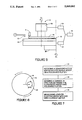
- FIG. 1 is an enlarged side elevation view of a portion of a semiconductor wafer prior to mechanical planarization
- FIG. 2 is an enlarged side elevation view of a portion of a semiconductor wafer after mechanical planarization
- FIG. 3 is a plan view of a semiconductor wafer
- FIG. 4 is a side elevation view of FIG. 3;
- FIG. 5 is a schematic view of mechanical planarization apparatus having endpoint detection apparatus constructed in accordance with the invention.
- FIG. 6 is a schematic plan view showing rotation of a polishing platen and polishing head for mechanical planarization of a semiconductor wafer.
- FIG. 7 is a block diagram of a method of endpoint detection in accordance with the invention during mechanical planarization of semiconductor wafer.
- a semiconductor wafer typically includes a substrate on which a plurality of micro devices have been formed.
- the wafer substrate is typically formed of a single crystal silicon material.
- the micro devices are formed by patterning regions on the substrate and patterning layers on the substrate.
- a chemical mechanical planarization process may be utilized, for instance, to remove a portion of a layer. Different layers are generally formed of different materials.
- During formation regions or vias on the silicon substrate may be patterned for contact with a plurality of IC devices as shown in FIG. 1.
- An insulating or oxide coating may then be formed or deposited on the substrate and over the IC devices. As shown in FIG. 2, it may be necessary to remove the oxide coating to the level of the IC devices to form insulating spacers therebetween. This can be accomplished by a chemical mechanical planarization process.
- a chemical mechanical planarization process involves mechanically polishing a thin, flat semiconductor wafer under controlled pressure, temperature, time, and chemical conditions.
- a semiconductor wafer is shown in FIGS. 3 and 4 and is generally designated as 10.
- the wafer is generally circular in shape and includes a major flat 12.
- the size of the wafer 10 is typically about 5 inches in diameter but may be several inches smaller or longer.
- a plurality of patterned dies are formed o the surface of the wafer, each having a micro topography.
- the micro topography of each patterned die can be altered as illustrated by the example of FIGS. 1 and 2 by the mechanical planarization process.
- mechanical planarization can be utilized to form other wafer topography and in the polishing, cleaning, and planing of the wafer surface.
- different layers of the semiconductor wafer are formed of different materials (i.e. metallic film, polysilicon film, insulators) which have a different relative hardness.
- the IC devices formed in FIGS. 1 and 2 are generally harder than the oxide coating formed thereon.
- the method and apparatus of the invention utilizes this relative difference between materials to detect planar endpoints during the mechanical planarization process.
- the mechanical planarization apparatus 14 includes:
- polishing means in the form of a rotatable polishing platen 16 and a polishing agent 18 which is applied t the surface of the polishing platen 16;
- holding means for holding the semiconductor wafer 10 in the form of a rotatable polishing head 20 mounted for holding and rotating the wafer 10 against the polishing platen 16 under a controlled force F;
- endpoint detection means in the form of motor current meters 22,24 which measure the load or amperage on electric drive motors 26,28 for the polishing platen 16 and polishing head 20 and sense a change in friction between the wafer 10 and the polishing platen 16.
- the polishing head 20 holds the wafer 10 for rotation against the polishing platen 16 under a controlled force (F).
- F a controlled force
- a direction of rotation of the polishing platen 16 and polishing head 20 is preferably the same. This is shown in FIG. 6. (Alternately, the polishing platen 16 and polishing head 20 may be rotated in opposite directions). Additionally, the polishing head 20 is constructed to move across the polishing platen 16 as indicated by the double headed arrow in FIG. 6.
- the polishing agent 18 is dispensed as shown in FIG. 5 through a suitable valved conduit onto the surface of the polishing platen 16.
- Such mechanical planarization apparatus are well known in the art.
- One such apparatus is manufactured by Westech Engineering and designated as a Model 372 Polisher.
- the apparatus of the invention adds the current meters 22,24 to the drive motors 26,28 of the planarization apparatus of the prior art in order to detect the amperage or load on the motors 26,28.
- Such current meters 22,24 must necessarily be sensitive to small variations in current, but are commercially available in the art.
- the current meters 22,24 constantly monitor the force required to rotate the wafer 10 on the polishing platen 16. Any change in this force will signal the change in friction of the exposed surface of the wafer 10, which occurs at a planar endpoint.
- the load or amperage draw of the motors 26,28 is a function of the force (F) exerted by the polishing head 20 and wafer 10 on the polishing platen 16. Additionally, the load is a function of the coefficient of friction between the wafer 10, polishing slurry 18, and polishing platen 16. A change in the coefficient of friction between these surfaces will change the load or amperage draw of the drive motors 26,28. If, for example, the oxide coating of a wafer 10, as shown in FIG. 1, is removed to the plane of the tops of the (IC) devices the change in coefficient of friction can be detected by a different amperage draw of the current meters 22,24. The point at which the coefficient of friction changes is thus equated to a planar endpoint of the wafer 10.
- the current of either the polishing platen drive motor 26 or the polishing head drive motor 28 or both may be monitored. This change can be utilized to generate a signal from the current meters 22,24 to a control means 36 (FIG. 5), which stops or adjusts apparatus and the mechanical planarization process as required.
- control means 36 could be formed by equipment and procedures known in the art and may include visual signals and manual controls.
- the method of the invention is adapted to detect the endpoint of a planarized wafer surface in such an apparatus and can be summarized by the steps of:
- step 32 sensing a change in friction between the surface of the wafer 10 and the polishing platen 16, step 32.
- sensing of a change in friction is accomplished by measuring the load on electric drive motors 26,28 with current meters 22,24, step 34.
- This change in friction between the surface of the wafer and the polishing platen 16 can then be equated to a planar endpoint of the wafer surface.
- This concept can be more fully explained with reference to FIGS. 1 and 2.
- the oxide surface (FIG. 1) of the wafer 10 contacts the surface of the polishing platen 16.
- the oxide surface has a hardness which produces a certain coefficient of friction by contact with the surface of the polishing platen 16 and polishing agent 18.
- the surface of the polishing platen 16 may typically be formed of a relatively soft material such as blown polyurethane.
- This coefficient of friction is generally constant until the oxide is polished away to the point in which the surface of the IC devices is exposed (FIG. 2). At this point, the IC devices contact the surface of the polishing platen 16.
- the IC devices may be formed of a harder material than the oxide coating (for example, a metallic film may be contacted).
- a different coefficient of friction thus occurs between the surface of the wafer 10 and the surface of the polishing platen 16. Assuming the downward force F (FIG. 5) on the wafer 10 and the rotational speed of the polishing head 20 and polishing platen 16 remains constant, this different coefficient of friction will produce a different load on the electric drive motors 26,28. This load can be sensed by the current meters 22,24. A planar endpoint in which the oxide coating has been removed to the top of the IC devices is thus detected.
- This change in coefficient of friction between the planar surfaces, although relatively small, is subjected to a multiplying factor if the current draw on the drive motor 26 for the polishing platen 16 is monitored.
- the multiplying factor can be determined as follows.
- the electric drive motor 26 for the polishing platen 16 produces a torque (T) which is opposed by the rotating polishing head 10.
- This torque (T) is also related to the force (F) (FIG. 5) pressing the polishing head 20 against the polishing platen 16.
- force (F) is also related to but is different than the coefficient of friction between the surface of the wafer 10, polishing slurry 18, and polishing platen 16.
- a small change in the coefficient of friction between the surfaces can thus be detected as a change in the torque (T) seen by the electric drive motors 26 (and, thus, the current flow) multiplied by the radius (r).
- the invention thus provides a simple yet unobvious method and apparatus for detecting the planar endpoint of a semiconductor wafer during a mechanical planarization process. While the process of the invention has been described with reference to a preferred embodiment thereof, as will be apparent to those skilled in the art, certain changes and modifications can be made without departing from the scope of the invention as defined by the following claims.
Abstract
Description
Claims (9)
Priority Applications (1)
| Application Number | Priority Date | Filing Date | Title |
|---|---|---|---|
| US07/686,686 US5069002A (en) | 1991-04-17 | 1991-04-17 | Apparatus for endpoint detection during mechanical planarization of semiconductor wafers |
Applications Claiming Priority (1)
| Application Number | Priority Date | Filing Date | Title |
|---|---|---|---|
| US07/686,686 US5069002A (en) | 1991-04-17 | 1991-04-17 | Apparatus for endpoint detection during mechanical planarization of semiconductor wafers |
Publications (1)
| Publication Number | Publication Date |
|---|---|
| US5069002A true US5069002A (en) | 1991-12-03 |
Family
ID=24757316
Family Applications (1)
| Application Number | Title | Priority Date | Filing Date |
|---|---|---|---|
| US07/686,686 Expired - Lifetime US5069002A (en) | 1991-04-17 | 1991-04-17 | Apparatus for endpoint detection during mechanical planarization of semiconductor wafers |
Country Status (1)
| Country | Link |
|---|---|
| US (1) | US5069002A (en) |
Cited By (167)
| Publication number | Priority date | Publication date | Assignee | Title |
|---|---|---|---|---|
| US5244527A (en) * | 1991-08-06 | 1993-09-14 | Nec Corporation | Manufacturing unit for semiconductor devices |
| US5245794A (en) * | 1992-04-09 | 1993-09-21 | Advanced Micro Devices, Inc. | Audio end point detector for chemical-mechanical polishing and method therefor |
| US5298110A (en) * | 1991-06-06 | 1994-03-29 | Lsi Logic Corporation | Trench planarization techniques |
| US5312770A (en) * | 1991-06-06 | 1994-05-17 | Lsi Logic Corporation | Techniques for forming isolation structures |
| US5314107A (en) * | 1992-12-31 | 1994-05-24 | Motorola, Inc. | Automated method for joining wafers |
| US5399528A (en) * | 1989-06-01 | 1995-03-21 | Leibovitz; Jacques | Multi-layer fabrication in integrated circuit systems |
| US5413966A (en) * | 1990-12-20 | 1995-05-09 | Lsi Logic Corporation | Shallow trench etch |
| US5439551A (en) * | 1994-03-02 | 1995-08-08 | Micron Technology, Inc. | Chemical-mechanical polishing techniques and methods of end point detection in chemical-mechanical polishing processes |
| US5483568A (en) * | 1994-11-03 | 1996-01-09 | Kabushiki Kaisha Toshiba | Pad condition and polishing rate monitor using fluorescence |
| US5486265A (en) * | 1995-02-06 | 1996-01-23 | Advanced Micro Devices, Inc. | Chemical-mechanical polishing of thin materials using a pulse polishing technique |
| US5486129A (en) * | 1993-08-25 | 1996-01-23 | Micron Technology, Inc. | System and method for real-time control of semiconductor a wafer polishing, and a polishing head |
| US5514616A (en) * | 1991-08-26 | 1996-05-07 | Lsi Logic Corporation | Depositing and densifying glass to planarize layers in semi-conductor devices based on CMOS structures |
| US5527423A (en) * | 1994-10-06 | 1996-06-18 | Cabot Corporation | Chemical mechanical polishing slurry for metal layers |
| US5534106A (en) * | 1994-07-26 | 1996-07-09 | Kabushiki Kaisha Toshiba | Apparatus for processing semiconductor wafers |
| US5539592A (en) * | 1994-10-05 | 1996-07-23 | International Business Machines Corporation | System and method for monitoring friction between head and disk to predict head disk interaction failure in direct access storage devices |
| US5552996A (en) * | 1995-02-16 | 1996-09-03 | International Business Machines Corporation | Method and system using the design pattern of IC chips in the processing thereof |
| GB2298961A (en) * | 1992-05-26 | 1996-09-18 | Toshiba Kk | polishing apparatus |
| US5567199A (en) * | 1993-10-21 | 1996-10-22 | Wacker-Chemitronic Gesellschaft fur Elektronik-Grundstoffe AG | Workpiece holder for rotary grinding machines for grinding semiconductor wafers, and method of positioning the workpiece holder |
| US5582534A (en) * | 1993-12-27 | 1996-12-10 | Applied Materials, Inc. | Orbital chemical mechanical polishing apparatus and method |
| US5595526A (en) * | 1994-11-30 | 1997-01-21 | Intel Corporation | Method and apparatus for endpoint detection in a chemical/mechanical process for polishing a substrate |
| US5597341A (en) * | 1992-05-26 | 1997-01-28 | Kabushiki Kaisha Toshiba | Semiconductor planarizing apparatus |
| US5607341A (en) | 1994-08-08 | 1997-03-04 | Leach; Michael A. | Method and structure for polishing a wafer during manufacture of integrated circuits |
| US5609718A (en) * | 1995-09-29 | 1997-03-11 | Micron Technology, Inc. | Method and apparatus for measuring a change in the thickness of polishing pads used in chemical-mechanical planarization of semiconductor wafers |
| US5609511A (en) * | 1994-04-14 | 1997-03-11 | Hitachi, Ltd. | Polishing method |
| US5620286A (en) * | 1994-11-09 | 1997-04-15 | Rank Taylor Hobson, Ltd. | Flycutting machine for manufacturing printed circuit boards |
| EP0771611A1 (en) * | 1995-11-02 | 1997-05-07 | Ebara Corporation | Method and apparatus for determining endpoint in polishing process |
| US5639388A (en) * | 1995-01-19 | 1997-06-17 | Ebara Corporation | Polishing endpoint detection method |
| WO1997022442A1 (en) * | 1995-12-19 | 1997-06-26 | Applied Materials, Inc. | Determining the coefficient of friction of a polishing pad |
| US5643046A (en) * | 1994-02-21 | 1997-07-01 | Kabushiki Kaisha Toshiba | Polishing method and apparatus for detecting a polishing end point of a semiconductor wafer |
| US5643060A (en) * | 1993-08-25 | 1997-07-01 | Micron Technology, Inc. | System for real-time control of semiconductor wafer polishing including heater |
| US5643053A (en) * | 1993-12-27 | 1997-07-01 | Applied Materials, Inc. | Chemical mechanical polishing apparatus with improved polishing control |
| US5643048A (en) * | 1996-02-13 | 1997-07-01 | Micron Technology, Inc. | Endpoint regulator and method for regulating a change in wafer thickness in chemical-mechanical planarization of semiconductor wafers |
| US5650039A (en) * | 1994-03-02 | 1997-07-22 | Applied Materials, Inc. | Chemical mechanical polishing apparatus with improved slurry distribution |
| US5659492A (en) * | 1996-03-19 | 1997-08-19 | International Business Machines Corporation | Chemical mechanical polishing endpoint process control |
| US5658183A (en) * | 1993-08-25 | 1997-08-19 | Micron Technology, Inc. | System for real-time control of semiconductor wafer polishing including optical monitoring |
| US5676587A (en) * | 1995-12-06 | 1997-10-14 | International Business Machines Corporation | Selective polish process for titanium, titanium nitride, tantalum and tantalum nitride |
| US5685766A (en) * | 1995-11-30 | 1997-11-11 | Speedfam Corporation | Polishing control method |
| US5695384A (en) * | 1994-12-07 | 1997-12-09 | Texas Instruments Incorporated | Chemical-mechanical polishing salt slurry |
| US5700180A (en) * | 1993-08-25 | 1997-12-23 | Micron Technology, Inc. | System for real-time control of semiconductor wafer polishing |
| US5705435A (en) * | 1996-08-09 | 1998-01-06 | Industrial Technology Research Institute | Chemical-mechanical polishing (CMP) apparatus |
| DE19652839A1 (en) * | 1996-07-09 | 1998-01-22 | Lg Semicon Co Ltd | Level sensor for chemical-mechanical polishing device for semiconductor wafer |
| US5722875A (en) * | 1995-05-30 | 1998-03-03 | Tokyo Electron Limited | Method and apparatus for polishing |
| US5733175A (en) | 1994-04-25 | 1998-03-31 | Leach; Michael A. | Polishing a workpiece using equal velocity at all points overlapping a polisher |
| US5738562A (en) * | 1996-01-24 | 1998-04-14 | Micron Technology, Inc. | Apparatus and method for planar end-point detection during chemical-mechanical polishing |
| US5738568A (en) * | 1996-10-04 | 1998-04-14 | International Business Machines Corporation | Flexible tilted wafer carrier |
| US5766058A (en) * | 1995-02-10 | 1998-06-16 | Advanced Micro Devices, Inc. | Chemical-mechanical polishing using curved carriers |
| US5769691A (en) * | 1996-06-14 | 1998-06-23 | Speedfam Corp | Methods and apparatus for the chemical mechanical planarization of electronic devices |
| US5846882A (en) * | 1996-10-03 | 1998-12-08 | Applied Materials, Inc. | Endpoint detector for a chemical mechanical polishing system |
| US5860847A (en) * | 1995-09-06 | 1999-01-19 | Ebara Corporation | Polishing apparatus |
| US5865665A (en) * | 1997-02-14 | 1999-02-02 | Yueh; William | In-situ endpoint control apparatus for semiconductor wafer polishing process |
| US5893754A (en) * | 1996-05-21 | 1999-04-13 | Micron Technology, Inc. | Method for chemical-mechanical planarization of stop-on-feature semiconductor wafers |
| US5904608A (en) * | 1996-05-30 | 1999-05-18 | Ebara Corporation | Polishing apparatus having interlock function |
| US5938504A (en) * | 1993-11-16 | 1999-08-17 | Applied Materials, Inc. | Substrate polishing apparatus |
| US5949927A (en) * | 1992-12-28 | 1999-09-07 | Tang; Wallace T. Y. | In-situ real-time monitoring technique and apparatus for endpoint detection of thin films during chemical/mechanical polishing planarization |
| US5948700A (en) * | 1996-05-20 | 1999-09-07 | Chartered Semiconductor Manufacturing Ltd. | Method of planarization of an intermetal dielectric layer using chemical mechanical polishing |
| US6004188A (en) * | 1998-09-10 | 1999-12-21 | Chartered Semiconductor Manufacturing Ltd. | Method for forming copper damascene structures by using a dual CMP barrier layer |
| US6007408A (en) * | 1997-08-21 | 1999-12-28 | Micron Technology, Inc. | Method and apparatus for endpointing mechanical and chemical-mechanical polishing of substrates |
| US6046111A (en) * | 1998-09-02 | 2000-04-04 | Micron Technology, Inc. | Method and apparatus for endpointing mechanical and chemical-mechanical planarization of microelectronic substrates |
| US6062952A (en) * | 1997-06-05 | 2000-05-16 | Robinson; Karl M. | Planarization process with abrasive polishing slurry that is selective to a planarized surface |
| US6117779A (en) * | 1998-12-15 | 2000-09-12 | Lsi Logic Corporation | Endpoint detection method and apparatus which utilize a chelating agent to detect a polishing endpoint |
| EP1052064A2 (en) * | 1999-05-05 | 2000-11-15 | Applied Materials, Inc. | Chemical mechanical polishing with friction-based control |
| DE19949976C1 (en) * | 1999-10-08 | 2000-11-16 | Univ Dresden Tech | In-situ end-point detection process, for chemical-mechanical polishing of semiconductor wafer layers, uses an ion-selective electrode to monitor ion concentration changes in a polishing slurry and reagent solution mixture |
| US6168683B1 (en) | 1998-02-24 | 2001-01-02 | Speedfam-Ipec Corporation | Apparatus and method for the face-up surface treatment of wafers |
| US6191037B1 (en) | 1998-09-03 | 2001-02-20 | Micron Technology, Inc. | Methods, apparatuses and substrate assembly structures for fabricating microelectronic components using mechanical and chemical-mechanical planarization processes |
| USRE37104E1 (en) | 1993-08-12 | 2001-03-20 | Micron Technology, Inc. | Planarization of a gate electrode for improved gate patterning over non-planar active area isolation |
| US6203407B1 (en) | 1998-09-03 | 2001-03-20 | Micron Technology, Inc. | Method and apparatus for increasing-chemical-polishing selectivity |
| US6213846B1 (en) | 1999-07-12 | 2001-04-10 | International Business Machines Corporation | Real-time control of chemical-mechanical polishing processes using a shaft distortion measurement |
| US6217418B1 (en) | 1999-04-14 | 2001-04-17 | Advanced Micro Devices, Inc. | Polishing pad and method for polishing porous materials |
| US6238273B1 (en) * | 1999-08-31 | 2001-05-29 | Micron Technology, Inc. | Methods for predicting polishing parameters of polishing pads and methods and machines for planarizing microelectronic substrate assemblies in mechanical or chemical-mechanical planarization |
| US6261851B1 (en) * | 1999-09-30 | 2001-07-17 | International Business Machines Corporation | Optimization of CMP process by detecting of oxide/nitride interface using IR system |
| US6267644B1 (en) | 1998-11-06 | 2001-07-31 | Beaver Creek Concepts Inc | Fixed abrasive finishing element having aids finishing method |
| US6269510B1 (en) | 1999-01-04 | 2001-08-07 | International Business Machines Corporation | Post CMP clean brush with torque monitor |
| US6287171B1 (en) * | 2000-02-15 | 2001-09-11 | Speedfam-Ipec Corporation | System and method for detecting CMP endpoint via direct chemical monitoring of reactions |
| US6291349B1 (en) | 1999-03-25 | 2001-09-18 | Beaver Creek Concepts Inc | Abrasive finishing with partial organic boundary layer |
| US6290572B1 (en) | 2000-03-23 | 2001-09-18 | Micron Technology, Inc. | Devices and methods for in-situ control of mechanical or chemical-mechanical planarization of microelectronic-device substrate assemblies |
| US6293845B1 (en) * | 1999-09-04 | 2001-09-25 | Mitsubishi Materials Corporation | System and method for end-point detection in a multi-head CMP tool using real-time monitoring of motor current |
| US6334807B1 (en) | 1999-04-30 | 2002-01-01 | International Business Machines Corporation | Chemical mechanical polishing in-situ end point system |
| WO2002009907A1 (en) * | 2000-07-31 | 2002-02-07 | Asml Us, Inc. | Method of chemical mechanical polishing |
| US6346202B1 (en) | 1999-03-25 | 2002-02-12 | Beaver Creek Concepts Inc | Finishing with partial organic boundary layer |
| US6368181B1 (en) | 1995-05-23 | 2002-04-09 | Nova Measuring Instruments Ltd. | Apparatus for optical inspection of wafers during polishing |
| DE19726665C2 (en) * | 1997-06-23 | 2002-06-27 | Univ Dresden Tech | Process and arrangement for in-situ endpoint determination at the CMP |
| US6428399B1 (en) * | 1994-05-23 | 2002-08-06 | Sumitomo Electric Industries, Ltd. | Polishing apparatus for polishing a hard material-coated wafer |
| US6428388B2 (en) | 1998-11-06 | 2002-08-06 | Beaver Creek Concepts Inc. | Finishing element with finishing aids |
| US20020127496A1 (en) * | 2000-08-31 | 2002-09-12 | Blalock Guy T. | Methods and apparatuses for making and using planarizing pads for mechanical and chemical-mechanical planarization of microelectronic substrates |
| US20020124957A1 (en) * | 1999-08-31 | 2002-09-12 | Hofmann James J. | Methods and apparatuses for monitoring and controlling mechanical or chemical-mechanical planarization of microelectronic substrate assemblies |
| US20020137448A1 (en) * | 2000-07-31 | 2002-09-26 | Suh Nam P. | Apparatus and method for chemical mechanical polishing of substrates |
| US6458015B1 (en) | 1996-11-06 | 2002-10-01 | Micron Technology, Inc. | Chemical-mechanical planarization machine and method for uniformly planarizing semiconductor wafers |
| US6511576B2 (en) | 1999-11-17 | 2003-01-28 | Micron Technology, Inc. | System for planarizing microelectronic substrates having apertures |
| US20030045100A1 (en) * | 2000-07-31 | 2003-03-06 | Massachusetts Institute Of Technology | In-situ method and apparatus for end point detection in chemical mechanical polishing |
| US6533893B2 (en) | 1999-09-02 | 2003-03-18 | Micron Technology, Inc. | Method and apparatus for chemical-mechanical planarization of microelectronic substrates with selected planarizing liquids |
| US6541381B2 (en) | 1998-11-06 | 2003-04-01 | Beaver Creek Concepts Inc | Finishing method for semiconductor wafers using a lubricating boundary layer |
| US6548407B1 (en) | 2000-04-26 | 2003-04-15 | Micron Technology, Inc. | Method and apparatus for controlling chemical interactions during planarization of microelectronic substrates |
| US6551933B1 (en) | 1999-03-25 | 2003-04-22 | Beaver Creek Concepts Inc | Abrasive finishing with lubricant and tracking |
| US6568989B1 (en) | 1999-04-01 | 2003-05-27 | Beaver Creek Concepts Inc | Semiconductor wafer finishing control |
| US6576553B2 (en) | 1999-05-11 | 2003-06-10 | Micron Technology, Inc. | Chemical mechanical planarization of conductive material |
| US6612901B1 (en) | 2000-06-07 | 2003-09-02 | Micron Technology, Inc. | Apparatus for in-situ optical endpointing of web-format planarizing machines in mechanical or chemical-mechanical planarization of microelectronic-device substrate assemblies |
| US6628410B2 (en) | 1996-02-16 | 2003-09-30 | Micron Technology, Inc. | Endpoint detector and method for measuring a change in wafer thickness in chemical-mechanical polishing of semiconductor wafers and other microelectronic substrates |
| US6634927B1 (en) | 1998-11-06 | 2003-10-21 | Charles J Molnar | Finishing element using finishing aids |
| US6656023B1 (en) * | 1998-11-06 | 2003-12-02 | Beaver Creek Concepts Inc | In situ control with lubricant and tracking |
| US6666749B2 (en) | 2001-08-30 | 2003-12-23 | Micron Technology, Inc. | Apparatus and method for enhanced processing of microelectronic workpieces |
| US6666754B1 (en) * | 2000-01-18 | 2003-12-23 | Advanced Micro Devices, Inc. | Method and apparatus for determining CMP pad conditioner effectiveness |
| US20040005845A1 (en) * | 2002-04-26 | 2004-01-08 | Tomohiko Kitajima | Polishing method and apparatus |
| US20040038623A1 (en) * | 2002-08-26 | 2004-02-26 | Nagasubramaniyan Chandrasekaran | Methods and systems for conditioning planarizing pads used in planarizing substrates |
| US6722943B2 (en) | 2001-08-24 | 2004-04-20 | Micron Technology, Inc. | Planarizing machines and methods for dispensing planarizing solutions in the processing of microelectronic workpieces |
| US6741913B2 (en) | 2001-12-11 | 2004-05-25 | International Business Machines Corporation | Technique for noise reduction in a torque-based chemical-mechanical polishing endpoint detection system |
| US6739947B1 (en) | 1998-11-06 | 2004-05-25 | Beaver Creek Concepts Inc | In situ friction detector method and apparatus |
| US20040115841A1 (en) * | 2001-09-20 | 2004-06-17 | Molnar Charles J. | In situ finishing aid control |
| US6780086B2 (en) * | 2001-10-12 | 2004-08-24 | Mosel Vitelic, Inc. | Determining an endpoint in a polishing process |
| US6796883B1 (en) | 2001-03-15 | 2004-09-28 | Beaver Creek Concepts Inc | Controlled lubricated finishing |
| US20040214509A1 (en) * | 2003-04-28 | 2004-10-28 | Elledge Jason B. | Systems and methods for mechanical and/or chemical-mechanical polishing of microfeature workpieces |
| US6833046B2 (en) | 2000-05-04 | 2004-12-21 | Micron Technology, Inc. | Planarizing machines and methods for mechanical and/or chemical-mechanical planarization of microelectronic-device substrate assemblies |
| US20040259472A1 (en) * | 2003-04-01 | 2004-12-23 | Chalmers Scott A. | Whole-substrate spectral imaging system for CMP |
| US6841991B2 (en) | 2002-08-29 | 2005-01-11 | Micron Technology, Inc. | Planarity diagnostic system, E.G., for microelectronic component test systems |
| US20050009450A1 (en) * | 1995-05-23 | 2005-01-13 | Nova Measuring Instruments Ltd | Apparatus for optical inspection of wafers during processing |
| US6860798B2 (en) | 2002-08-08 | 2005-03-01 | Micron Technology, Inc. | Carrier assemblies, planarizing apparatuses including carrier assemblies, and methods for planarizing micro-device workpieces |
| US6866566B2 (en) | 2001-08-24 | 2005-03-15 | Micron Technology, Inc. | Apparatus and method for conditioning a contact surface of a processing pad used in processing microelectronic workpieces |
| US6869498B1 (en) | 2002-02-04 | 2005-03-22 | Applied Materials, Inc. | Chemical mechanical polishing with shear force measurement |
| US6869335B2 (en) | 2002-07-08 | 2005-03-22 | Micron Technology, Inc. | Retaining rings, planarizing apparatuses including retaining rings, and methods for planarizing micro-device workpieces |
| US6872132B2 (en) | 2003-03-03 | 2005-03-29 | Micron Technology, Inc. | Systems and methods for monitoring characteristics of a polishing pad used in polishing micro-device workpieces |
| US20050079804A1 (en) * | 2003-10-09 | 2005-04-14 | Taylor Theodore M. | Planarizing solutions including abrasive elements, and methods for manufacturing and using such planarizing solutions |
| US6884152B2 (en) | 2003-02-11 | 2005-04-26 | Micron Technology, Inc. | Apparatuses and methods for conditioning polishing pads used in polishing micro-device workpieces |
| US6922253B2 (en) | 2000-08-30 | 2005-07-26 | Micron Technology, Inc. | Planarizing machines and control systems for mechanical and/or chemical-mechanical planarization of microelectronic substrates |
| US6935929B2 (en) | 2003-04-28 | 2005-08-30 | Micron Technology, Inc. | Polishing machines including under-pads and methods for mechanical and/or chemical-mechanical polishing of microfeature workpieces |
| US6939198B1 (en) | 2001-12-28 | 2005-09-06 | Applied Materials, Inc. | Polishing system with in-line and in-situ metrology |
| US20050197048A1 (en) * | 2004-03-04 | 2005-09-08 | Leping Li | Method for manufacturing a workpiece and torque transducer module |
| US6958001B2 (en) | 2002-08-23 | 2005-10-25 | Micron Technology, Inc. | Carrier assemblies, planarizing apparatuses including carrier assemblies, and methods for planarizing micro-device workpieces |
| US6995068B1 (en) | 2000-06-09 | 2006-02-07 | Newport Fab, Llc | Double-implant high performance varactor and method for manufacturing same |
| US20060037699A1 (en) * | 2002-11-27 | 2006-02-23 | Masahiko Nakamori | Polishing pad and method for manufacturing semiconductor device |
| US7030603B2 (en) | 2003-08-21 | 2006-04-18 | Micron Technology, Inc. | Apparatuses and methods for monitoring rotation of a conductive microfeature workpiece |
| US7033253B2 (en) | 2004-08-12 | 2006-04-25 | Micron Technology, Inc. | Polishing pad conditioners having abrasives and brush elements, and associated systems and methods |
| US7033251B2 (en) | 2003-01-16 | 2006-04-25 | Micron Technology, Inc. | Carrier assemblies, polishing machines including carrier assemblies, and methods for polishing micro-device workpieces |
| US7037403B1 (en) | 1992-12-28 | 2006-05-02 | Applied Materials Inc. | In-situ real-time monitoring technique and apparatus for detection of thin films during chemical/mechanical polishing planarization |
| US7040954B1 (en) * | 2004-09-28 | 2006-05-09 | Lam Research Corporation | Methods of and apparatus for controlling polishing surface characteristics for chemical mechanical polishing |
| US7066792B2 (en) | 2004-08-06 | 2006-06-27 | Micron Technology, Inc. | Shaped polishing pads for beveling microfeature workpiece edges, and associate system and methods |
| US20060148386A1 (en) * | 2003-07-15 | 2006-07-06 | Hoya Corporation | Method and device for manufacturing substrate for magnetic disk, and method of manufacturing magnetic disk |
| US7086927B2 (en) | 2004-03-09 | 2006-08-08 | Micron Technology, Inc. | Methods and systems for planarizing workpieces, e.g., microelectronic workpieces |
| US7094695B2 (en) | 2002-08-21 | 2006-08-22 | Micron Technology, Inc. | Apparatus and method for conditioning a polishing pad used for mechanical and/or chemical-mechanical planarization |
| US7115016B2 (en) | 2002-08-29 | 2006-10-03 | Micron Technology, Inc. | Apparatus and method for mechanical and/or chemical-mechanical planarization of micro-device workpieces |
| US7131889B1 (en) | 2002-03-04 | 2006-11-07 | Micron Technology, Inc. | Method for planarizing microelectronic workpieces |
| US7131890B1 (en) * | 1998-11-06 | 2006-11-07 | Beaver Creek Concepts, Inc. | In situ finishing control |
| US7182669B2 (en) | 2002-07-18 | 2007-02-27 | Micron Technology, Inc. | Methods and systems for planarizing workpieces, e.g., microelectronic workpieces |
| US20070087662A1 (en) * | 2003-10-31 | 2007-04-19 | Benvegnu Dominic J | Friction sensor for polishing system |
| US7220164B1 (en) * | 2003-12-08 | 2007-05-22 | Beaver Creek Concepts Inc | Advanced finishing control |
| US20070190905A1 (en) * | 2004-03-11 | 2007-08-16 | Tetsuo Shimomura | Polishing pad and semiconductor device manufacturing method |
| DE102006018276A1 (en) * | 2006-04-20 | 2007-10-31 | Conti Temic Microelectronic Gmbh | Sample body polishing finishing method, involves monitoring polishing of body by temporally disintegrated measuring of actual force exerted on body, and completing polishing when actual strength strongly varies from given default value |
| US7294041B1 (en) * | 2006-08-31 | 2007-11-13 | Inha-Industry Partnership Institute | Moving head for semiconductor wafer polishing apparatus |
| US20070287364A1 (en) * | 2004-07-26 | 2007-12-13 | Atsushi Shigeta | Substrate processing method and substrate processing apparatus |
| US7326105B2 (en) | 2005-08-31 | 2008-02-05 | Micron Technology, Inc. | Retaining rings, and associated planarizing apparatuses, and related methods for planarizing micro-device workpieces |
| US20080071414A1 (en) * | 2006-09-14 | 2008-03-20 | Tokyo Seimitsu Co., Ltd | Polishing end point detection method utilizing torque change and device thereof |
| US7513818B2 (en) | 2003-10-31 | 2009-04-07 | Applied Materials, Inc. | Polishing endpoint detection system and method using friction sensor |
| US20090093202A1 (en) * | 2006-04-19 | 2009-04-09 | Toyo Tire & Rubber Co., Ltd. | Method for manufacturing polishing pad |
| DE102008045216A1 (en) | 2007-08-23 | 2009-04-09 | Technische Universität Dresden | Method for in-situ end point detection during chemical-mechanical polishing of semiconductor material layers of semiconductor wafer using polishing machine, involves making potential change to occur during polishing |
| US20090253353A1 (en) * | 2004-12-10 | 2009-10-08 | Toyo Tire & Rubber Co., Ltd | Polishing pad |
| US20100162631A1 (en) * | 2007-05-31 | 2010-07-01 | Toyo Tire & Rubber Co., Ltd. | Process for manufacturing polishing pad |
| US8005634B2 (en) | 2002-03-22 | 2011-08-23 | Applied Materials, Inc. | Copper wiring module control |
| CN101670541B (en) * | 2009-09-15 | 2012-05-23 | 厦门大学 | Fast polishing traversing processing method of heavy-calibre planar optical elements |
| US20130115854A1 (en) * | 2011-11-07 | 2013-05-09 | Taiwan Semiconductor Manufacturing Company, Ltd. | End Point Detection in Grinding |
| US20130217306A1 (en) * | 2012-02-16 | 2013-08-22 | Taiwan Semiconductor Manufacturing Co., Ltd. | CMP Groove Depth and Conditioning Disk Monitoring |
| US20130288572A1 (en) * | 2012-04-26 | 2013-10-31 | Applied Materials, Inc. | Linear Prediction For Filtering Of Data During In-Situ Monitoring Of Polishing |
| CN104493683A (en) * | 2014-11-28 | 2015-04-08 | 上海华力微电子有限公司 | Method for testing film grinding speed |
| US9358660B2 (en) | 2011-11-07 | 2016-06-07 | Taiwan Semiconductor Manufacturing Company, Ltd. | Grinding wheel design with elongated teeth arrangement |
| US20190039206A1 (en) * | 2017-08-04 | 2019-02-07 | Toshiba Memory Corporation | Polishing device, polishing method, and record medium |
| US11282755B2 (en) | 2019-08-27 | 2022-03-22 | Applied Materials, Inc. | Asymmetry correction via oriented wafer loading |
| US20220281066A1 (en) * | 2021-03-03 | 2022-09-08 | Applied Materials, Inc. | Motor torque endpoint during polishing with spatial resolution |
| US11446783B2 (en) | 2018-03-12 | 2022-09-20 | Applied Materials, Inc. | Filtering during in-situ monitoring of polishing |
| US11504821B2 (en) | 2017-11-16 | 2022-11-22 | Applied Materials, Inc. | Predictive filter for polishing pad wear rate monitoring |
| US11660722B2 (en) | 2018-08-31 | 2023-05-30 | Applied Materials, Inc. | Polishing system with capacitive shear sensor |
Citations (13)
| Publication number | Priority date | Publication date | Assignee | Title |
|---|---|---|---|---|
| US3699722A (en) * | 1970-11-23 | 1972-10-24 | Radiation Inc | Precision polishing of semiconductor crystal wafers |
| US3841031A (en) * | 1970-10-21 | 1974-10-15 | Monsanto Co | Process for polishing thin elements |
| US3979239A (en) * | 1974-12-30 | 1976-09-07 | Monsanto Company | Process for chemical-mechanical polishing of III-V semiconductor materials |
| US4193226A (en) * | 1977-09-21 | 1980-03-18 | Kayex Corporation | Polishing apparatus |
| US4358338A (en) * | 1980-05-16 | 1982-11-09 | Varian Associates, Inc. | End point detection method for physical etching process |
| US4407094A (en) * | 1981-11-03 | 1983-10-04 | Transat Corp. | Apparatus for automatic lapping control |
| US4663890A (en) * | 1982-05-18 | 1987-05-12 | Gmn Georg Muller Nurnberg Gmbh | Method for machining workpieces of brittle hard material into wafers |
| US4793895A (en) * | 1988-01-25 | 1988-12-27 | Ibm Corporation | In situ conductivity monitoring technique for chemical/mechanical planarization endpoint detection |
| US4811522A (en) * | 1987-03-23 | 1989-03-14 | Gill Jr Gerald L | Counterbalanced polishing apparatus |
| US4879258A (en) * | 1988-08-31 | 1989-11-07 | Texas Instruments Incorporated | Integrated circuit planarization by mechanical polishing |
| US4910155A (en) * | 1988-10-28 | 1990-03-20 | International Business Machines Corporation | Wafer flood polishing |
| US4914868A (en) * | 1988-09-28 | 1990-04-10 | International Business Machines Corporation | Lapping control system for magnetic transducers |
| US4956313A (en) * | 1987-08-17 | 1990-09-11 | International Business Machines Corporation | Via-filling and planarization technique |
-
1991
- 1991-04-17 US US07/686,686 patent/US5069002A/en not_active Expired - Lifetime
Patent Citations (13)
| Publication number | Priority date | Publication date | Assignee | Title |
|---|---|---|---|---|
| US3841031A (en) * | 1970-10-21 | 1974-10-15 | Monsanto Co | Process for polishing thin elements |
| US3699722A (en) * | 1970-11-23 | 1972-10-24 | Radiation Inc | Precision polishing of semiconductor crystal wafers |
| US3979239A (en) * | 1974-12-30 | 1976-09-07 | Monsanto Company | Process for chemical-mechanical polishing of III-V semiconductor materials |
| US4193226A (en) * | 1977-09-21 | 1980-03-18 | Kayex Corporation | Polishing apparatus |
| US4358338A (en) * | 1980-05-16 | 1982-11-09 | Varian Associates, Inc. | End point detection method for physical etching process |
| US4407094A (en) * | 1981-11-03 | 1983-10-04 | Transat Corp. | Apparatus for automatic lapping control |
| US4663890A (en) * | 1982-05-18 | 1987-05-12 | Gmn Georg Muller Nurnberg Gmbh | Method for machining workpieces of brittle hard material into wafers |
| US4811522A (en) * | 1987-03-23 | 1989-03-14 | Gill Jr Gerald L | Counterbalanced polishing apparatus |
| US4956313A (en) * | 1987-08-17 | 1990-09-11 | International Business Machines Corporation | Via-filling and planarization technique |
| US4793895A (en) * | 1988-01-25 | 1988-12-27 | Ibm Corporation | In situ conductivity monitoring technique for chemical/mechanical planarization endpoint detection |
| US4879258A (en) * | 1988-08-31 | 1989-11-07 | Texas Instruments Incorporated | Integrated circuit planarization by mechanical polishing |
| US4914868A (en) * | 1988-09-28 | 1990-04-10 | International Business Machines Corporation | Lapping control system for magnetic transducers |
| US4910155A (en) * | 1988-10-28 | 1990-03-20 | International Business Machines Corporation | Wafer flood polishing |
Cited By (309)
| Publication number | Priority date | Publication date | Assignee | Title |
|---|---|---|---|---|
| US5399528A (en) * | 1989-06-01 | 1995-03-21 | Leibovitz; Jacques | Multi-layer fabrication in integrated circuit systems |
| US5413966A (en) * | 1990-12-20 | 1995-05-09 | Lsi Logic Corporation | Shallow trench etch |
| US5298110A (en) * | 1991-06-06 | 1994-03-29 | Lsi Logic Corporation | Trench planarization techniques |
| US5312770A (en) * | 1991-06-06 | 1994-05-17 | Lsi Logic Corporation | Techniques for forming isolation structures |
| US5441094A (en) * | 1991-06-06 | 1995-08-15 | Lsi Logic Corporation | Trench planarization techniques |
| US5244527A (en) * | 1991-08-06 | 1993-09-14 | Nec Corporation | Manufacturing unit for semiconductor devices |
| US5514616A (en) * | 1991-08-26 | 1996-05-07 | Lsi Logic Corporation | Depositing and densifying glass to planarize layers in semi-conductor devices based on CMOS structures |
| US5874327A (en) * | 1991-08-26 | 1999-02-23 | Lsi Logic Corporation | Fabricating a semiconductor device using precursor CMOS semiconductor substrate of a given configuration |
| US5554555A (en) * | 1991-08-26 | 1996-09-10 | Lsi Logic Corporation | Planarizing by polishing techniques for fabricating semiconductor devices based on CMOS structures |
| US5245794A (en) * | 1992-04-09 | 1993-09-21 | Advanced Micro Devices, Inc. | Audio end point detector for chemical-mechanical polishing and method therefor |
| US5597341A (en) * | 1992-05-26 | 1997-01-28 | Kabushiki Kaisha Toshiba | Semiconductor planarizing apparatus |
| US5914275A (en) * | 1992-05-26 | 1999-06-22 | Kabushiki Kaisha Toshiba | Polishing apparatus and method for planarizing layer on a semiconductor wafer |
| US5948205A (en) * | 1992-05-26 | 1999-09-07 | Kabushiki Kaisha Toshiba | Polishing apparatus and method for planarizing layer on a semiconductor wafer |
| GB2298961B (en) * | 1992-05-26 | 1997-01-08 | Toshiba Kk | Polishing apparatus for planarizing layer on a semiconductor wafer |
| GB2298960B (en) * | 1992-05-26 | 1997-01-08 | Toshiba Kk | Polishing apparatus and method for planarizing layer on a semiconductor wafer |
| GB2298960A (en) * | 1992-05-26 | 1996-09-18 | Toshiba Kk | Polishing apparatus and method |
| GB2298961A (en) * | 1992-05-26 | 1996-09-18 | Toshiba Kk | polishing apparatus |
| US7569119B2 (en) | 1992-12-28 | 2009-08-04 | Applied Materials, Inc. | In-situ real-time monitoring technique and apparatus for detection of thin films during chemical/mechanical polishing planarization |
| US20080060758A1 (en) * | 1992-12-28 | 2008-03-13 | Applied Materials, Inc. | Apparatus for detection of thin films during chemical/mechanical polishing planarization |
| US20060151111A1 (en) * | 1992-12-28 | 2006-07-13 | Tang Wallace T Y | In-situ real-time monitoring technique and apparatus for detection of thin films during chemical/mechanical polishing planarization |
| US7037403B1 (en) | 1992-12-28 | 2006-05-02 | Applied Materials Inc. | In-situ real-time monitoring technique and apparatus for detection of thin films during chemical/mechanical polishing planarization |
| US7582183B2 (en) | 1992-12-28 | 2009-09-01 | Applied Materials, Inc. | Apparatus for detection of thin films during chemical/mechanical polishing planarization |
| US5949927A (en) * | 1992-12-28 | 1999-09-07 | Tang; Wallace T. Y. | In-situ real-time monitoring technique and apparatus for endpoint detection of thin films during chemical/mechanical polishing planarization |
| US7024063B2 (en) | 1992-12-28 | 2006-04-04 | Applied Materials Inc. | In-situ real-time monitoring technique and apparatus for endpoint detection of thin films during chemical/mechanical polishing planarization |
| US20050146728A1 (en) * | 1992-12-28 | 2005-07-07 | Tang Wallace T.Y. | In-situ real-time monitoring technique and apparatus for endpoint detection of thin films during chemical/mechanical polishing planarization |
| US6849152B2 (en) | 1992-12-28 | 2005-02-01 | Applied Materials, Inc. | In-situ real-time monitoring technique and apparatus for endpoint detection of thin films during chemical/mechanical polishing planarization |
| US6614529B1 (en) | 1992-12-28 | 2003-09-02 | Applied Materials, Inc. | In-situ real-time monitoring technique and apparatus for endpoint detection of thin films during chemical/mechanical polishing planarization |
| US5314107A (en) * | 1992-12-31 | 1994-05-24 | Motorola, Inc. | Automated method for joining wafers |
| USRE37104E1 (en) | 1993-08-12 | 2001-03-20 | Micron Technology, Inc. | Planarization of a gate electrode for improved gate patterning over non-planar active area isolation |
| US6739944B2 (en) | 1993-08-25 | 2004-05-25 | Micron Technology, Inc. | System for real-time control of semiconductor wafer polishing |
| US5700180A (en) * | 1993-08-25 | 1997-12-23 | Micron Technology, Inc. | System for real-time control of semiconductor wafer polishing |
| US6464561B2 (en) | 1993-08-25 | 2002-10-15 | Micron Technology, Inc. | System for real-time control of semiconductor wafer polishing |
| US5486129A (en) * | 1993-08-25 | 1996-01-23 | Micron Technology, Inc. | System and method for real-time control of semiconductor a wafer polishing, and a polishing head |
| US5851135A (en) * | 1993-08-25 | 1998-12-22 | Micron Technology, Inc. | System for real-time control of semiconductor wafer polishing |
| US6120347A (en) * | 1993-08-25 | 2000-09-19 | Micron Technology, Inc. | System for real-time control of semiconductor wafer polishing |
| US5643060A (en) * | 1993-08-25 | 1997-07-01 | Micron Technology, Inc. | System for real-time control of semiconductor wafer polishing including heater |
| US5762537A (en) * | 1993-08-25 | 1998-06-09 | Micron Technology, Inc. | System for real-time control of semiconductor wafer polishing including heater |
| US6338667B2 (en) | 1993-08-25 | 2002-01-15 | Micron Technology, Inc. | System for real-time control of semiconductor wafer polishing |
| US6464560B2 (en) | 1993-08-25 | 2002-10-15 | Micron Technology, Inc. | System for real-time control of semiconductor wafer polishing |
| US6464564B2 (en) | 1993-08-25 | 2002-10-15 | Micron Technology, Inc. | System for real-time control of semiconductor wafer polishing |
| US5658183A (en) * | 1993-08-25 | 1997-08-19 | Micron Technology, Inc. | System for real-time control of semiconductor wafer polishing including optical monitoring |
| US6306009B1 (en) | 1993-08-25 | 2001-10-23 | Micron Technology, Inc. | System for real-time control of semiconductor wafer polishing |
| US5730642A (en) * | 1993-08-25 | 1998-03-24 | Micron Technology, Inc. | System for real-time control of semiconductor wafer polishing including optical montoring |
| US6261151B1 (en) | 1993-08-25 | 2001-07-17 | Micron Technology, Inc. | System for real-time control of semiconductor wafer polishing |
| US5842909A (en) * | 1993-08-25 | 1998-12-01 | Micron Technology, Inc. | System for real-time control of semiconductor wafer polishing including heater |
| US5567199A (en) * | 1993-10-21 | 1996-10-22 | Wacker-Chemitronic Gesellschaft fur Elektronik-Grundstoffe AG | Workpiece holder for rotary grinding machines for grinding semiconductor wafers, and method of positioning the workpiece holder |
| US5938504A (en) * | 1993-11-16 | 1999-08-17 | Applied Materials, Inc. | Substrate polishing apparatus |
| US6179690B1 (en) | 1993-11-16 | 2001-01-30 | Applied Materials, Inc. | Substrate polishing apparatus |
| US5582534A (en) * | 1993-12-27 | 1996-12-10 | Applied Materials, Inc. | Orbital chemical mechanical polishing apparatus and method |
| US5899800A (en) * | 1993-12-27 | 1999-05-04 | Applied Materials, Inc. | Chemical mechanical polishing apparatus with orbital polishing |
| US6503134B2 (en) | 1993-12-27 | 2003-01-07 | Applied Materials, Inc. | Carrier head for a chemical mechanical polishing apparatus |
| US5643053A (en) * | 1993-12-27 | 1997-07-01 | Applied Materials, Inc. | Chemical mechanical polishing apparatus with improved polishing control |
| US5643046A (en) * | 1994-02-21 | 1997-07-01 | Kabushiki Kaisha Toshiba | Polishing method and apparatus for detecting a polishing end point of a semiconductor wafer |
| US5650039A (en) * | 1994-03-02 | 1997-07-22 | Applied Materials, Inc. | Chemical mechanical polishing apparatus with improved slurry distribution |
| US5439551A (en) * | 1994-03-02 | 1995-08-08 | Micron Technology, Inc. | Chemical-mechanical polishing techniques and methods of end point detection in chemical-mechanical polishing processes |
| US5609511A (en) * | 1994-04-14 | 1997-03-11 | Hitachi, Ltd. | Polishing method |
| US5733175A (en) | 1994-04-25 | 1998-03-31 | Leach; Michael A. | Polishing a workpiece using equal velocity at all points overlapping a polisher |
| US6428399B1 (en) * | 1994-05-23 | 2002-08-06 | Sumitomo Electric Industries, Ltd. | Polishing apparatus for polishing a hard material-coated wafer |
| US5534106A (en) * | 1994-07-26 | 1996-07-09 | Kabushiki Kaisha Toshiba | Apparatus for processing semiconductor wafers |
| US5593537A (en) * | 1994-07-26 | 1997-01-14 | Kabushiki Kaisha Toshiba | Apparatus for processing semiconductor wafers |
| US5607341A (en) | 1994-08-08 | 1997-03-04 | Leach; Michael A. | Method and structure for polishing a wafer during manufacture of integrated circuits |
| US5836807A (en) | 1994-08-08 | 1998-11-17 | Leach; Michael A. | Method and structure for polishing a wafer during manufacture of integrated circuits |
| US5702290A (en) | 1994-08-08 | 1997-12-30 | Leach; Michael A. | Block for polishing a wafer during manufacture of integrated circuits |
| US5539592A (en) * | 1994-10-05 | 1996-07-23 | International Business Machines Corporation | System and method for monitoring friction between head and disk to predict head disk interaction failure in direct access storage devices |
| US5527423A (en) * | 1994-10-06 | 1996-06-18 | Cabot Corporation | Chemical mechanical polishing slurry for metal layers |
| US5483568A (en) * | 1994-11-03 | 1996-01-09 | Kabushiki Kaisha Toshiba | Pad condition and polishing rate monitor using fluorescence |
| US5620286A (en) * | 1994-11-09 | 1997-04-15 | Rank Taylor Hobson, Ltd. | Flycutting machine for manufacturing printed circuit boards |
| US5595526A (en) * | 1994-11-30 | 1997-01-21 | Intel Corporation | Method and apparatus for endpoint detection in a chemical/mechanical process for polishing a substrate |
| US5695384A (en) * | 1994-12-07 | 1997-12-09 | Texas Instruments Incorporated | Chemical-mechanical polishing salt slurry |
| US5639388A (en) * | 1995-01-19 | 1997-06-17 | Ebara Corporation | Polishing endpoint detection method |
| US5486265A (en) * | 1995-02-06 | 1996-01-23 | Advanced Micro Devices, Inc. | Chemical-mechanical polishing of thin materials using a pulse polishing technique |
| US5766058A (en) * | 1995-02-10 | 1998-06-16 | Advanced Micro Devices, Inc. | Chemical-mechanical polishing using curved carriers |
| US5552996A (en) * | 1995-02-16 | 1996-09-03 | International Business Machines Corporation | Method and system using the design pattern of IC chips in the processing thereof |
| US20020051135A1 (en) * | 1995-05-23 | 2002-05-02 | Nova Measuring Instruments Ltd. | Apparatus for optical inspection of wafers during polishing |
| US20050164608A2 (en) * | 1995-05-23 | 2005-07-28 | Nova Measuring Instruments Ltd. | Apparatus for optical inspection of wafers during processing |
| US6368181B1 (en) | 1995-05-23 | 2002-04-09 | Nova Measuring Instruments Ltd. | Apparatus for optical inspection of wafers during polishing |
| US6752689B2 (en) | 1995-05-23 | 2004-06-22 | Nova Measuring Instruments Ltd. | Apparatus for optical inspection of wafers during polishing |
| US7169015B2 (en) | 1995-05-23 | 2007-01-30 | Nova Measuring Instruments Ltd. | Apparatus for optical inspection of wafers during processing |
| US20050009450A1 (en) * | 1995-05-23 | 2005-01-13 | Nova Measuring Instruments Ltd | Apparatus for optical inspection of wafers during processing |
| US5722875A (en) * | 1995-05-30 | 1998-03-03 | Tokyo Electron Limited | Method and apparatus for polishing |
| US5860847A (en) * | 1995-09-06 | 1999-01-19 | Ebara Corporation | Polishing apparatus |
| US5609718A (en) * | 1995-09-29 | 1997-03-11 | Micron Technology, Inc. | Method and apparatus for measuring a change in the thickness of polishing pads used in chemical-mechanical planarization of semiconductor wafers |
| US5801066A (en) * | 1995-09-29 | 1998-09-01 | Micron Technology, Inc. | Method and apparatus for measuring a change in the thickness of polishing pads used in chemical-mechanical planarization of semiconductor wafers |
| US5830041A (en) * | 1995-11-02 | 1998-11-03 | Ebara Corporation | Method and apparatus for determining endpoint during a polishing process |
| EP0771611A1 (en) * | 1995-11-02 | 1997-05-07 | Ebara Corporation | Method and apparatus for determining endpoint in polishing process |
| US5685766A (en) * | 1995-11-30 | 1997-11-11 | Speedfam Corporation | Polishing control method |
| US5676587A (en) * | 1995-12-06 | 1997-10-14 | International Business Machines Corporation | Selective polish process for titanium, titanium nitride, tantalum and tantalum nitride |
| WO1997022442A1 (en) * | 1995-12-19 | 1997-06-26 | Applied Materials, Inc. | Determining the coefficient of friction of a polishing pad |
| US5743784A (en) * | 1995-12-19 | 1998-04-28 | Applied Materials, Inc. | Apparatus and method to determine the coefficient of friction of a chemical mechanical polishing pad during a pad conditioning process and to use it to control the process |
| US5738562A (en) * | 1996-01-24 | 1998-04-14 | Micron Technology, Inc. | Apparatus and method for planar end-point detection during chemical-mechanical polishing |
| US5643048A (en) * | 1996-02-13 | 1997-07-01 | Micron Technology, Inc. | Endpoint regulator and method for regulating a change in wafer thickness in chemical-mechanical planarization of semiconductor wafers |
| US6628410B2 (en) | 1996-02-16 | 2003-09-30 | Micron Technology, Inc. | Endpoint detector and method for measuring a change in wafer thickness in chemical-mechanical polishing of semiconductor wafers and other microelectronic substrates |
| US5659492A (en) * | 1996-03-19 | 1997-08-19 | International Business Machines Corporation | Chemical mechanical polishing endpoint process control |
| US5948700A (en) * | 1996-05-20 | 1999-09-07 | Chartered Semiconductor Manufacturing Ltd. | Method of planarization of an intermetal dielectric layer using chemical mechanical polishing |
| US5893754A (en) * | 1996-05-21 | 1999-04-13 | Micron Technology, Inc. | Method for chemical-mechanical planarization of stop-on-feature semiconductor wafers |
| US5904608A (en) * | 1996-05-30 | 1999-05-18 | Ebara Corporation | Polishing apparatus having interlock function |
| US5769691A (en) * | 1996-06-14 | 1998-06-23 | Speedfam Corp | Methods and apparatus for the chemical mechanical planarization of electronic devices |
| US7083501B1 (en) | 1996-06-14 | 2006-08-01 | Speedfam-Ipec Corporation | Methods and apparatus for the chemical mechanical planarization of electronic devices |
| DE19652839C2 (en) * | 1996-07-09 | 2002-04-18 | Lg Semicon Co Ltd | Level sensor device and method for semiconductor wafers for a chemical mechanical polishing device |
| DE19652839A1 (en) * | 1996-07-09 | 1998-01-22 | Lg Semicon Co Ltd | Level sensor for chemical-mechanical polishing device for semiconductor wafer |
| US5705435A (en) * | 1996-08-09 | 1998-01-06 | Industrial Technology Research Institute | Chemical-mechanical polishing (CMP) apparatus |
| US5846882A (en) * | 1996-10-03 | 1998-12-08 | Applied Materials, Inc. | Endpoint detector for a chemical mechanical polishing system |
| US5738568A (en) * | 1996-10-04 | 1998-04-14 | International Business Machines Corporation | Flexible tilted wafer carrier |
| US6458015B1 (en) | 1996-11-06 | 2002-10-01 | Micron Technology, Inc. | Chemical-mechanical planarization machine and method for uniformly planarizing semiconductor wafers |
| US5865665A (en) * | 1997-02-14 | 1999-02-02 | Yueh; William | In-situ endpoint control apparatus for semiconductor wafer polishing process |
| US6379225B1 (en) | 1997-06-05 | 2002-04-30 | Micron Technology, Inc. | Planarization process with abrasive polishing slurry that is selective to a planarized surface |
| US6062952A (en) * | 1997-06-05 | 2000-05-16 | Robinson; Karl M. | Planarization process with abrasive polishing slurry that is selective to a planarized surface |
| DE19726665C2 (en) * | 1997-06-23 | 2002-06-27 | Univ Dresden Tech | Process and arrangement for in-situ endpoint determination at the CMP |
| US6007408A (en) * | 1997-08-21 | 1999-12-28 | Micron Technology, Inc. | Method and apparatus for endpointing mechanical and chemical-mechanical polishing of substrates |
| USRE39547E1 (en) * | 1997-08-21 | 2007-04-03 | Micron Technology, Inc. | Method and apparatus for endpointing mechanical and chemical-mechanical polishing of substrates |
| US6168683B1 (en) | 1998-02-24 | 2001-01-02 | Speedfam-Ipec Corporation | Apparatus and method for the face-up surface treatment of wafers |
| US6046111A (en) * | 1998-09-02 | 2000-04-04 | Micron Technology, Inc. | Method and apparatus for endpointing mechanical and chemical-mechanical planarization of microelectronic substrates |
| US6325702B2 (en) | 1998-09-03 | 2001-12-04 | Micron Technology, Inc. | Method and apparatus for increasing chemical-mechanical-polishing selectivity |
| US6645865B2 (en) * | 1998-09-03 | 2003-11-11 | Micron Technology, Inc. | Methods, apparatuses and substrate assembly structures for fabricating microelectronic components using mechanical and chemical-mechanical planarization processes |
| US6613675B2 (en) | 1998-09-03 | 2003-09-02 | Micron Technology, Inc. | Methods, apparatuses, and substrate assembly structures for fabricating microelectronic components using mechanical and chemical-mechanical planarization processes |
| US6893325B2 (en) | 1998-09-03 | 2005-05-17 | Micron Technology, Inc. | Method and apparatus for increasing chemical-mechanical-polishing selectivity |
| US6552408B2 (en) * | 1998-09-03 | 2003-04-22 | Micron Technology, Inc. | Methods, apparatuses, and substrate assembly structures for fabricating microelectronic components using mechanical and chemical-mechanical planarization processes |
| US6191037B1 (en) | 1998-09-03 | 2001-02-20 | Micron Technology, Inc. | Methods, apparatuses and substrate assembly structures for fabricating microelectronic components using mechanical and chemical-mechanical planarization processes |
| US20010009811A1 (en) * | 1998-09-03 | 2001-07-26 | Robinson Karl M. | Methods, apparatuses, and substrate assembly structures for fabricating microelectronic components using mechanical and chemical-mechanical planarization processes |
| US6203407B1 (en) | 1998-09-03 | 2001-03-20 | Micron Technology, Inc. | Method and apparatus for increasing-chemical-polishing selectivity |
| US7132035B2 (en) * | 1998-09-03 | 2006-11-07 | Micron Technology, Inc. | Methods, apparatuses, and substrate assembly structures for fabricating microelectronic components using mechanical and chemical-mechanical planarization processes |
| US6004188A (en) * | 1998-09-10 | 1999-12-21 | Chartered Semiconductor Manufacturing Ltd. | Method for forming copper damascene structures by using a dual CMP barrier layer |
| US6739947B1 (en) | 1998-11-06 | 2004-05-25 | Beaver Creek Concepts Inc | In situ friction detector method and apparatus |
| US7131890B1 (en) * | 1998-11-06 | 2006-11-07 | Beaver Creek Concepts, Inc. | In situ finishing control |
| US6541381B2 (en) | 1998-11-06 | 2003-04-01 | Beaver Creek Concepts Inc | Finishing method for semiconductor wafers using a lubricating boundary layer |
| US6656023B1 (en) * | 1998-11-06 | 2003-12-02 | Beaver Creek Concepts Inc | In situ control with lubricant and tracking |
| US6634927B1 (en) | 1998-11-06 | 2003-10-21 | Charles J Molnar | Finishing element using finishing aids |
| US6267644B1 (en) | 1998-11-06 | 2001-07-31 | Beaver Creek Concepts Inc | Fixed abrasive finishing element having aids finishing method |
| US6428388B2 (en) | 1998-11-06 | 2002-08-06 | Beaver Creek Concepts Inc. | Finishing element with finishing aids |
| US6117779A (en) * | 1998-12-15 | 2000-09-12 | Lsi Logic Corporation | Endpoint detection method and apparatus which utilize a chelating agent to detect a polishing endpoint |
| US6352596B2 (en) | 1999-01-04 | 2002-03-05 | International Business Machines Corporation | Post CMP cleaning method using a brush cleaner with torque monitor |
| US6269510B1 (en) | 1999-01-04 | 2001-08-07 | International Business Machines Corporation | Post CMP clean brush with torque monitor |
| US6291349B1 (en) | 1999-03-25 | 2001-09-18 | Beaver Creek Concepts Inc | Abrasive finishing with partial organic boundary layer |
| US6346202B1 (en) | 1999-03-25 | 2002-02-12 | Beaver Creek Concepts Inc | Finishing with partial organic boundary layer |
| US6551933B1 (en) | 1999-03-25 | 2003-04-22 | Beaver Creek Concepts Inc | Abrasive finishing with lubricant and tracking |
| US6568989B1 (en) | 1999-04-01 | 2003-05-27 | Beaver Creek Concepts Inc | Semiconductor wafer finishing control |
| US6217418B1 (en) | 1999-04-14 | 2001-04-17 | Advanced Micro Devices, Inc. | Polishing pad and method for polishing porous materials |
| US6334807B1 (en) | 1999-04-30 | 2002-01-01 | International Business Machines Corporation | Chemical mechanical polishing in-situ end point system |
| US6887129B2 (en) | 1999-05-05 | 2005-05-03 | Applied Materials, Inc. | Chemical mechanical polishing with friction-based control |
| EP1052064A3 (en) * | 1999-05-05 | 2003-01-22 | Applied Materials, Inc. | Chemical mechanical polishing with friction-based control |
| US6623334B1 (en) * | 1999-05-05 | 2003-09-23 | Applied Materials, Inc. | Chemical mechanical polishing with friction-based control |
| EP1052064A2 (en) * | 1999-05-05 | 2000-11-15 | Applied Materials, Inc. | Chemical mechanical polishing with friction-based control |
| US20040072500A1 (en) * | 1999-05-05 | 2004-04-15 | Manoocher Birang | Chemical mechanical polishing with friction-based control |
| US7045454B1 (en) * | 1999-05-11 | 2006-05-16 | Micron Technology, Inc. | Chemical mechanical planarization of conductive material |
| US6576553B2 (en) | 1999-05-11 | 2003-06-10 | Micron Technology, Inc. | Chemical mechanical planarization of conductive material |
| US6213846B1 (en) | 1999-07-12 | 2001-04-10 | International Business Machines Corporation | Real-time control of chemical-mechanical polishing processes using a shaft distortion measurement |
| US6361400B2 (en) | 1999-08-31 | 2002-03-26 | Micron Technology, Inc. | Methods for predicting polishing parameters of polishing pads, and methods and machines for planarizing microelectronic substrate assemblies in mechanical or chemical-mechanical planarization |
| US6682628B2 (en) * | 1999-08-31 | 2004-01-27 | Micron Technology, Inc. | Methods and apparatuses for monitoring and controlling mechanical or chemical-mechanical planarization of microelectronic substrate assemblies |
| US20020124957A1 (en) * | 1999-08-31 | 2002-09-12 | Hofmann James J. | Methods and apparatuses for monitoring and controlling mechanical or chemical-mechanical planarization of microelectronic substrate assemblies |
| US6238273B1 (en) * | 1999-08-31 | 2001-05-29 | Micron Technology, Inc. | Methods for predicting polishing parameters of polishing pads and methods and machines for planarizing microelectronic substrate assemblies in mechanical or chemical-mechanical planarization |
| US6350180B2 (en) | 1999-08-31 | 2002-02-26 | Micron Technology, Inc. | Methods for predicting polishing parameters of polishing pads, and methods and machines for planarizing microelectronic substrate assemblies in mechanical or chemical-mechanical planarization |
| US6464824B1 (en) * | 1999-08-31 | 2002-10-15 | Micron Technology, Inc. | Methods and apparatuses for monitoring and controlling mechanical or chemical-mechanical planarization of microelectronic substrate assemblies |
| US6533893B2 (en) | 1999-09-02 | 2003-03-18 | Micron Technology, Inc. | Method and apparatus for chemical-mechanical planarization of microelectronic substrates with selected planarizing liquids |
| US6293845B1 (en) * | 1999-09-04 | 2001-09-25 | Mitsubishi Materials Corporation | System and method for end-point detection in a multi-head CMP tool using real-time monitoring of motor current |
| US6261851B1 (en) * | 1999-09-30 | 2001-07-17 | International Business Machines Corporation | Optimization of CMP process by detecting of oxide/nitride interface using IR system |
| DE19949976C1 (en) * | 1999-10-08 | 2000-11-16 | Univ Dresden Tech | In-situ end-point detection process, for chemical-mechanical polishing of semiconductor wafer layers, uses an ion-selective electrode to monitor ion concentration changes in a polishing slurry and reagent solution mixture |
| US6511576B2 (en) | 1999-11-17 | 2003-01-28 | Micron Technology, Inc. | System for planarizing microelectronic substrates having apertures |
| US6666754B1 (en) * | 2000-01-18 | 2003-12-23 | Advanced Micro Devices, Inc. | Method and apparatus for determining CMP pad conditioner effectiveness |
| US6287171B1 (en) * | 2000-02-15 | 2001-09-11 | Speedfam-Ipec Corporation | System and method for detecting CMP endpoint via direct chemical monitoring of reactions |
| US6547640B2 (en) | 2000-03-23 | 2003-04-15 | Micron Technology, Inc. | Devices and methods for in-situ control of mechanical or chemical-mechanical planarization of microelectronic-device substrate assemblies |
| US6290572B1 (en) | 2000-03-23 | 2001-09-18 | Micron Technology, Inc. | Devices and methods for in-situ control of mechanical or chemical-mechanical planarization of microelectronic-device substrate assemblies |
| US6579799B2 (en) | 2000-04-26 | 2003-06-17 | Micron Technology, Inc. | Method and apparatus for controlling chemical interactions during planarization of microelectronic substrates |
| US6548407B1 (en) | 2000-04-26 | 2003-04-15 | Micron Technology, Inc. | Method and apparatus for controlling chemical interactions during planarization of microelectronic substrates |
| US6833046B2 (en) | 2000-05-04 | 2004-12-21 | Micron Technology, Inc. | Planarizing machines and methods for mechanical and/or chemical-mechanical planarization of microelectronic-device substrate assemblies |
| US6986700B2 (en) | 2000-06-07 | 2006-01-17 | Micron Technology, Inc. | Apparatuses for in-situ optical endpointing on web-format planarizing machines in mechanical or chemical-mechanical planarization of microelectronic-device substrate assemblies |
| US6612901B1 (en) | 2000-06-07 | 2003-09-02 | Micron Technology, Inc. | Apparatus for in-situ optical endpointing of web-format planarizing machines in mechanical or chemical-mechanical planarization of microelectronic-device substrate assemblies |
| US7229338B2 (en) | 2000-06-07 | 2007-06-12 | Micron Technology, Inc. | Apparatuses and methods for in-situ optical endpointing on web-format planarizing machines in mechanical or chemical-mechanical planarization of microelectronic-device substrate assemblies |
| US6995068B1 (en) | 2000-06-09 | 2006-02-07 | Newport Fab, Llc | Double-implant high performance varactor and method for manufacturing same |
| WO2002009907A1 (en) * | 2000-07-31 | 2002-02-07 | Asml Us, Inc. | Method of chemical mechanical polishing |
| US6458013B1 (en) * | 2000-07-31 | 2002-10-01 | Asml Us, Inc. | Method of chemical mechanical polishing |
| US20030045100A1 (en) * | 2000-07-31 | 2003-03-06 | Massachusetts Institute Of Technology | In-situ method and apparatus for end point detection in chemical mechanical polishing |
| US20020137448A1 (en) * | 2000-07-31 | 2002-09-26 | Suh Nam P. | Apparatus and method for chemical mechanical polishing of substrates |
| US7029381B2 (en) | 2000-07-31 | 2006-04-18 | Aviza Technology, Inc. | Apparatus and method for chemical mechanical polishing of substrates |
| US6798529B2 (en) | 2000-07-31 | 2004-09-28 | Aviza Technology, Inc. | In-situ method and apparatus for end point detection in chemical mechanical polishing |
| US6922253B2 (en) | 2000-08-30 | 2005-07-26 | Micron Technology, Inc. | Planarizing machines and control systems for mechanical and/or chemical-mechanical planarization of microelectronic substrates |
| US20020127496A1 (en) * | 2000-08-31 | 2002-09-12 | Blalock Guy T. | Methods and apparatuses for making and using planarizing pads for mechanical and chemical-mechanical planarization of microelectronic substrates |
| US6652764B1 (en) | 2000-08-31 | 2003-11-25 | Micron Technology, Inc. | Methods and apparatuses for making and using planarizing pads for mechanical and chemical-mechanical planarization of microelectronic substrates |
| US7037179B2 (en) | 2000-08-31 | 2006-05-02 | Micron Technology, Inc. | Methods and apparatuses for making and using planarizing pads for mechanical and chemical-mechanical planarization of microelectronic substrates |
| US6746317B2 (en) | 2000-08-31 | 2004-06-08 | Micron Technology, Inc. | Methods and apparatuses for making and using planarizing pads for mechanical and chemical mechanical planarization of microelectronic substrates |
| US6758735B2 (en) | 2000-08-31 | 2004-07-06 | Micron Technology, Inc. | Methods and apparatuses for making and using planarizing pads for mechanical and chemical-mechanical planarization of microelectronic substrates |
| US6796883B1 (en) | 2001-03-15 | 2004-09-28 | Beaver Creek Concepts Inc | Controlled lubricated finishing |
| US7001254B2 (en) | 2001-08-24 | 2006-02-21 | Micron Technology, Inc. | Apparatus and method for conditioning a contact surface of a processing pad used in processing microelectronic workpieces |
| US7210989B2 (en) | 2001-08-24 | 2007-05-01 | Micron Technology, Inc. | Planarizing machines and methods for dispensing planarizing solutions in the processing of microelectronic workpieces |
| US6866566B2 (en) | 2001-08-24 | 2005-03-15 | Micron Technology, Inc. | Apparatus and method for conditioning a contact surface of a processing pad used in processing microelectronic workpieces |
| US7134944B2 (en) | 2001-08-24 | 2006-11-14 | Micron Technology, Inc. | Apparatus and method for conditioning a contact surface of a processing pad used in processing microelectronic workpieces |
| US7163447B2 (en) | 2001-08-24 | 2007-01-16 | Micron Technology, Inc. | Apparatus and method for conditioning a contact surface of a processing pad used in processing microelectronic workpieces |
| US6722943B2 (en) | 2001-08-24 | 2004-04-20 | Micron Technology, Inc. | Planarizing machines and methods for dispensing planarizing solutions in the processing of microelectronic workpieces |
| US7021996B2 (en) | 2001-08-24 | 2006-04-04 | Micron Technology, Inc. | Apparatus and method for conditioning a contact surface of a processing pad used in processing microelectronic workpieces |
| US6666749B2 (en) | 2001-08-30 | 2003-12-23 | Micron Technology, Inc. | Apparatus and method for enhanced processing of microelectronic workpieces |
| US7156717B2 (en) * | 2001-09-20 | 2007-01-02 | Molnar Charles J | situ finishing aid control |
| US20040115841A1 (en) * | 2001-09-20 | 2004-06-17 | Molnar Charles J. | In situ finishing aid control |
| US6780086B2 (en) * | 2001-10-12 | 2004-08-24 | Mosel Vitelic, Inc. | Determining an endpoint in a polishing process |
| US6741913B2 (en) | 2001-12-11 | 2004-05-25 | International Business Machines Corporation | Technique for noise reduction in a torque-based chemical-mechanical polishing endpoint detection system |
| US20060286904A1 (en) * | 2001-12-28 | 2006-12-21 | Applied Materials, Inc. | Polishing System With In-Line and In-Situ Metrology |
| US20100062684A1 (en) * | 2001-12-28 | 2010-03-11 | Applied Materials, Inc. | Polishing system with in-line and in-situ metrology |
| US20110195528A1 (en) * | 2001-12-28 | 2011-08-11 | Swedek Boguslaw A | Polishing system with in-line and in-situ metrology |
| US7101251B2 (en) | 2001-12-28 | 2006-09-05 | Applied Materials, Inc. | Polishing system with in-line and in-situ metrology |
| US6939198B1 (en) | 2001-12-28 | 2005-09-06 | Applied Materials, Inc. | Polishing system with in-line and in-situ metrology |
| US7927182B2 (en) | 2001-12-28 | 2011-04-19 | Applied Materials, Inc. | Polishing system with in-line and in-situ metrology |
| US7585202B2 (en) | 2001-12-28 | 2009-09-08 | Applied Materials, Inc. | Computer-implemented method for process control in chemical mechanical polishing |
| US7294039B2 (en) | 2001-12-28 | 2007-11-13 | Applied Materials, Inc. | Polishing system with in-line and in-situ metrology |
| US8460057B2 (en) | 2001-12-28 | 2013-06-11 | Applied Materials, Inc. | Computer-implemented process control in chemical mechanical polishing |
| US20050245170A1 (en) * | 2001-12-28 | 2005-11-03 | Applied Materials, Inc., A Delaware Corporation | Polishing system with in-line and in-situ metrology |
| US6869498B1 (en) | 2002-02-04 | 2005-03-22 | Applied Materials, Inc. | Chemical mechanical polishing with shear force measurement |
| US7131889B1 (en) | 2002-03-04 | 2006-11-07 | Micron Technology, Inc. | Method for planarizing microelectronic workpieces |
| US8005634B2 (en) | 2002-03-22 | 2011-08-23 | Applied Materials, Inc. | Copper wiring module control |
| US20040005845A1 (en) * | 2002-04-26 | 2004-01-08 | Tomohiko Kitajima | Polishing method and apparatus |
| US20060228991A1 (en) * | 2002-04-26 | 2006-10-12 | Applied Materials, Inc. A Delaware Corporation | Polishing method and apparatus |
| US7101252B2 (en) | 2002-04-26 | 2006-09-05 | Applied Materials | Polishing method and apparatus |
| US7189153B2 (en) | 2002-07-08 | 2007-03-13 | Micron Technology, Inc. | Retaining rings, planarizing apparatuses including retaining rings, and methods for planarizing micro-device workpieces |
| US6869335B2 (en) | 2002-07-08 | 2005-03-22 | Micron Technology, Inc. | Retaining rings, planarizing apparatuses including retaining rings, and methods for planarizing micro-device workpieces |
| US6962520B2 (en) | 2002-07-08 | 2005-11-08 | Micron Technology, Inc. | Retaining rings, planarizing apparatuses including retaining rings, and methods for planarizing micro-device workpieces |
| US7182669B2 (en) | 2002-07-18 | 2007-02-27 | Micron Technology, Inc. | Methods and systems for planarizing workpieces, e.g., microelectronic workpieces |
| US7341502B2 (en) | 2002-07-18 | 2008-03-11 | Micron Technology, Inc. | Methods and systems for planarizing workpieces, e.g., microelectronic workpieces |
| US7604527B2 (en) | 2002-07-18 | 2009-10-20 | Micron Technology, Inc. | Methods and systems for planarizing workpieces, e.g., microelectronic workpieces |
| US6893332B2 (en) | 2002-08-08 | 2005-05-17 | Micron Technology, Inc. | Carrier assemblies, planarizing apparatuses including carrier assemblies, and methods for planarizing micro-device workpieces |
| US6860798B2 (en) | 2002-08-08 | 2005-03-01 | Micron Technology, Inc. | Carrier assemblies, planarizing apparatuses including carrier assemblies, and methods for planarizing micro-device workpieces |
| US7094695B2 (en) | 2002-08-21 | 2006-08-22 | Micron Technology, Inc. | Apparatus and method for conditioning a polishing pad used for mechanical and/or chemical-mechanical planarization |
| US7147543B2 (en) | 2002-08-23 | 2006-12-12 | Micron Technology, Inc. | Carrier assemblies, planarizing apparatuses including carrier assemblies, and methods for planarizing micro-device workpieces |
| US6958001B2 (en) | 2002-08-23 | 2005-10-25 | Micron Technology, Inc. | Carrier assemblies, planarizing apparatuses including carrier assemblies, and methods for planarizing micro-device workpieces |
| US7004817B2 (en) | 2002-08-23 | 2006-02-28 | Micron Technology, Inc. | Carrier assemblies, planarizing apparatuses including carrier assemblies, and methods for planarizing micro-device workpieces |
| US7235000B2 (en) | 2002-08-26 | 2007-06-26 | Micron Technology, Inc. | Methods and systems for conditioning planarizing pads used in planarizing substrates |
| US20040038623A1 (en) * | 2002-08-26 | 2004-02-26 | Nagasubramaniyan Chandrasekaran | Methods and systems for conditioning planarizing pads used in planarizing substrates |
| US7314401B2 (en) | 2002-08-26 | 2008-01-01 | Micron Technology, Inc. | Methods and systems for conditioning planarizing pads used in planarizing substrates |
| US7163439B2 (en) | 2002-08-26 | 2007-01-16 | Micron Technology, Inc. | Methods and systems for conditioning planarizing pads used in planarizing substrates |
| US7201635B2 (en) | 2002-08-26 | 2007-04-10 | Micron Technology, Inc. | Methods and systems for conditioning planarizing pads used in planarizing substrates |
| US7011566B2 (en) | 2002-08-26 | 2006-03-14 | Micron Technology, Inc. | Methods and systems for conditioning planarizing pads used in planarizing substrates |
| US6841991B2 (en) | 2002-08-29 | 2005-01-11 | Micron Technology, Inc. | Planarity diagnostic system, E.G., for microelectronic component test systems |
| US7115016B2 (en) | 2002-08-29 | 2006-10-03 | Micron Technology, Inc. | Apparatus and method for mechanical and/or chemical-mechanical planarization of micro-device workpieces |
| US20060037699A1 (en) * | 2002-11-27 | 2006-02-23 | Masahiko Nakamori | Polishing pad and method for manufacturing semiconductor device |
| US8845852B2 (en) | 2002-11-27 | 2014-09-30 | Toyo Tire & Rubber Co., Ltd. | Polishing pad and method of producing semiconductor device |
| US7255630B2 (en) | 2003-01-16 | 2007-08-14 | Micron Technology, Inc. | Methods of manufacturing carrier heads for polishing micro-device workpieces |
| US7074114B2 (en) | 2003-01-16 | 2006-07-11 | Micron Technology, Inc. | Carrier assemblies, polishing machines including carrier assemblies, and methods for polishing micro-device workpieces |
| US7033251B2 (en) | 2003-01-16 | 2006-04-25 | Micron Technology, Inc. | Carrier assemblies, polishing machines including carrier assemblies, and methods for polishing micro-device workpieces |
| US7708622B2 (en) | 2003-02-11 | 2010-05-04 | Micron Technology, Inc. | Apparatuses and methods for conditioning polishing pads used in polishing micro-device workpieces |
| US20100197204A1 (en) * | 2003-02-11 | 2010-08-05 | Micron Technology, Inc. | Apparatuses and methods for conditioning polishing pads used in polishing micro-device workpieces |
| US7997958B2 (en) | 2003-02-11 | 2011-08-16 | Micron Technology, Inc. | Apparatuses and methods for conditioning polishing pads used in polishing micro-device workpieces |
| US6884152B2 (en) | 2003-02-11 | 2005-04-26 | Micron Technology, Inc. | Apparatuses and methods for conditioning polishing pads used in polishing micro-device workpieces |
| US6872132B2 (en) | 2003-03-03 | 2005-03-29 | Micron Technology, Inc. | Systems and methods for monitoring characteristics of a polishing pad used in polishing micro-device workpieces |
| US7033248B2 (en) | 2003-03-03 | 2006-04-25 | Micron Technology, Inc. | Systems and methods for monitoring characteristics of a polishing pad used in polishing micro-device workpieces |
| US7033246B2 (en) | 2003-03-03 | 2006-04-25 | Micron Technology, Inc. | Systems and methods for monitoring characteristics of a polishing pad used in polishing micro-device workpieces |
| US7070478B2 (en) | 2003-03-03 | 2006-07-04 | Micron Technology, Inc. | Systems and methods for monitoring characteristics of a polishing pad used in polishing micro-device workpieces |
| US7258596B2 (en) | 2003-03-03 | 2007-08-21 | Micron Technology, Inc. | Systems and methods for monitoring characteristics of a polishing pad used in polishing micro-device workpieces |
| US20040259472A1 (en) * | 2003-04-01 | 2004-12-23 | Chalmers Scott A. | Whole-substrate spectral imaging system for CMP |
| US6935929B2 (en) | 2003-04-28 | 2005-08-30 | Micron Technology, Inc. | Polishing machines including under-pads and methods for mechanical and/or chemical-mechanical polishing of microfeature workpieces |
| US20040214509A1 (en) * | 2003-04-28 | 2004-10-28 | Elledge Jason B. | Systems and methods for mechanical and/or chemical-mechanical polishing of microfeature workpieces |
| US7357695B2 (en) | 2003-04-28 | 2008-04-15 | Micron Technology, Inc. | Systems and methods for mechanical and/or chemical-mechanical polishing of microfeature workpieces |
| US7131891B2 (en) | 2003-04-28 | 2006-11-07 | Micron Technology, Inc. | Systems and methods for mechanical and/or chemical-mechanical polishing of microfeature workpieces |
| US7175511B2 (en) * | 2003-07-15 | 2007-02-13 | Hoya Corporation | Method of manufacturing substrate for magnetic disk, apparatus for manufacturing substrate for magnetic disk, and method of manufacturing magnetic disk |
| US20060148386A1 (en) * | 2003-07-15 | 2006-07-06 | Hoya Corporation | Method and device for manufacturing substrate for magnetic disk, and method of manufacturing magnetic disk |
| US7176676B2 (en) | 2003-08-21 | 2007-02-13 | Micron Technology, Inc. | Apparatuses and methods for monitoring rotation of a conductive microfeature workpiece |
| US7030603B2 (en) | 2003-08-21 | 2006-04-18 | Micron Technology, Inc. | Apparatuses and methods for monitoring rotation of a conductive microfeature workpiece |
| US7223297B2 (en) | 2003-10-09 | 2007-05-29 | Micron Technology, Inc. | Planarizing solutions including abrasive elements, and methods for manufacturing and using such planarizing solutions |
| US20050239382A1 (en) * | 2003-10-09 | 2005-10-27 | Micron Technology, Inc. | Planarizing solutions including abrasive elements, and methods for manufacturing and using such planarizing solutions |
| US20050079804A1 (en) * | 2003-10-09 | 2005-04-14 | Taylor Theodore M. | Planarizing solutions including abrasive elements, and methods for manufacturing and using such planarizing solutions |
| US6939211B2 (en) | 2003-10-09 | 2005-09-06 | Micron Technology, Inc. | Planarizing solutions including abrasive elements, and methods for manufacturing and using such planarizing solutions |
| US7727049B2 (en) | 2003-10-31 | 2010-06-01 | Applied Materials, Inc. | Friction sensor for polishing system |
| US8758086B2 (en) | 2003-10-31 | 2014-06-24 | Applied Materials, Inc. | Friction sensor for polishing system |
| US20070087662A1 (en) * | 2003-10-31 | 2007-04-19 | Benvegnu Dominic J | Friction sensor for polishing system |
| US20090253351A1 (en) * | 2003-10-31 | 2009-10-08 | Applied Materials, Inc. | Friction sensor for polishing system |
| US8342906B2 (en) | 2003-10-31 | 2013-01-01 | Applied Materials, Inc. | Friction sensor for polishing system |
| US7513818B2 (en) | 2003-10-31 | 2009-04-07 | Applied Materials, Inc. | Polishing endpoint detection system and method using friction sensor |
| US7220164B1 (en) * | 2003-12-08 | 2007-05-22 | Beaver Creek Concepts Inc | Advanced finishing control |
| US20050197048A1 (en) * | 2004-03-04 | 2005-09-08 | Leping Li | Method for manufacturing a workpiece and torque transducer module |
| US7416472B2 (en) | 2004-03-09 | 2008-08-26 | Micron Technology, Inc. | Systems for planarizing workpieces, e.g., microelectronic workpieces |
| US7086927B2 (en) | 2004-03-09 | 2006-08-08 | Micron Technology, Inc. | Methods and systems for planarizing workpieces, e.g., microelectronic workpieces |
| US7413500B2 (en) | 2004-03-09 | 2008-08-19 | Micron Technology, Inc. | Methods for planarizing workpieces, e.g., microelectronic workpieces |
| US20070190905A1 (en) * | 2004-03-11 | 2007-08-16 | Tetsuo Shimomura | Polishing pad and semiconductor device manufacturing method |
| US7731568B2 (en) | 2004-03-11 | 2010-06-08 | Toyo Tire & Rubber Co., Ltd. | Polishing pad and semiconductor device manufacturing method |
| US20070287364A1 (en) * | 2004-07-26 | 2007-12-13 | Atsushi Shigeta | Substrate processing method and substrate processing apparatus |
| US20100255757A1 (en) * | 2004-07-26 | 2010-10-07 | Atsushi Shigeta | Substrate processing method and substrate processing apparatus |
| US7767472B2 (en) | 2004-07-26 | 2010-08-03 | Ebara Corporation | Substrate processing method and substrate processing apparatus |
| US7210985B2 (en) | 2004-08-06 | 2007-05-01 | Micron Technology, Inc. | Shaped polishing pads for beveling microfeature workpiece edges, and associated systems and methods |
| US7066792B2 (en) | 2004-08-06 | 2006-06-27 | Micron Technology, Inc. | Shaped polishing pads for beveling microfeature workpiece edges, and associate system and methods |
| US7210984B2 (en) | 2004-08-06 | 2007-05-01 | Micron Technology, Inc. | Shaped polishing pads for beveling microfeature workpiece edges, and associated systems and methods |
| US7033253B2 (en) | 2004-08-12 | 2006-04-25 | Micron Technology, Inc. | Polishing pad conditioners having abrasives and brush elements, and associated systems and methods |
| US7040954B1 (en) * | 2004-09-28 | 2006-05-09 | Lam Research Corporation | Methods of and apparatus for controlling polishing surface characteristics for chemical mechanical polishing |
| US20090253353A1 (en) * | 2004-12-10 | 2009-10-08 | Toyo Tire & Rubber Co., Ltd | Polishing pad |
| US7871309B2 (en) | 2004-12-10 | 2011-01-18 | Toyo Tire & Rubber Co., Ltd. | Polishing pad |
| US7326105B2 (en) | 2005-08-31 | 2008-02-05 | Micron Technology, Inc. | Retaining rings, and associated planarizing apparatuses, and related methods for planarizing micro-device workpieces |
| US7347767B2 (en) | 2005-08-31 | 2008-03-25 | Micron Technology, Inc. | Retaining rings, and associated planarizing apparatuses, and related methods for planarizing micro-device workpieces |
| US20090093202A1 (en) * | 2006-04-19 | 2009-04-09 | Toyo Tire & Rubber Co., Ltd. | Method for manufacturing polishing pad |
| US8398794B2 (en) | 2006-04-19 | 2013-03-19 | Toyo Tire & Rubber Co., Ltd. | Method for manufacturing polishing pad |
| US8500932B2 (en) | 2006-04-19 | 2013-08-06 | Toyo Tire & Rubber Co., Ltd. | Method for manufacturing polishing pad |
| US9050707B2 (en) | 2006-04-19 | 2015-06-09 | Toyo Tire & Rubber Co., Ltd. | Method for manufacturing polishing pad |
| DE102006018276A1 (en) * | 2006-04-20 | 2007-10-31 | Conti Temic Microelectronic Gmbh | Sample body polishing finishing method, involves monitoring polishing of body by temporally disintegrated measuring of actual force exerted on body, and completing polishing when actual strength strongly varies from given default value |
| US7294041B1 (en) * | 2006-08-31 | 2007-11-13 | Inha-Industry Partnership Institute | Moving head for semiconductor wafer polishing apparatus |
| US8065031B2 (en) | 2006-09-14 | 2011-11-22 | Tokyo Seimitsu Co., Ltd | Polishing end point detection method utilizing torque change and device thereof |
| US20080071414A1 (en) * | 2006-09-14 | 2008-03-20 | Tokyo Seimitsu Co., Ltd | Polishing end point detection method utilizing torque change and device thereof |
| US8409308B2 (en) | 2007-05-31 | 2013-04-02 | Toyo Tire & Rubber Co., Ltd. | Process for manufacturing polishing pad |
| US20100162631A1 (en) * | 2007-05-31 | 2010-07-01 | Toyo Tire & Rubber Co., Ltd. | Process for manufacturing polishing pad |
| DE102008045216A1 (en) | 2007-08-23 | 2009-04-09 | Technische Universität Dresden | Method for in-situ end point detection during chemical-mechanical polishing of semiconductor material layers of semiconductor wafer using polishing machine, involves making potential change to occur during polishing |
| CN101670541B (en) * | 2009-09-15 | 2012-05-23 | 厦门大学 | Fast polishing traversing processing method of heavy-calibre planar optical elements |
| US20130115854A1 (en) * | 2011-11-07 | 2013-05-09 | Taiwan Semiconductor Manufacturing Company, Ltd. | End Point Detection in Grinding |
| US9358660B2 (en) | 2011-11-07 | 2016-06-07 | Taiwan Semiconductor Manufacturing Company, Ltd. | Grinding wheel design with elongated teeth arrangement |
| US9960088B2 (en) * | 2011-11-07 | 2018-05-01 | Taiwan Semiconductor Manufacturing Company, Ltd. | End point detection in grinding |
| US20130217306A1 (en) * | 2012-02-16 | 2013-08-22 | Taiwan Semiconductor Manufacturing Co., Ltd. | CMP Groove Depth and Conditioning Disk Monitoring |
| US20130288572A1 (en) * | 2012-04-26 | 2013-10-31 | Applied Materials, Inc. | Linear Prediction For Filtering Of Data During In-Situ Monitoring Of Polishing |
| US9308618B2 (en) * | 2012-04-26 | 2016-04-12 | Applied Materials, Inc. | Linear prediction for filtering of data during in-situ monitoring of polishing |
| CN104493683A (en) * | 2014-11-28 | 2015-04-08 | 上海华力微电子有限公司 | Method for testing film grinding speed |
| US20190039206A1 (en) * | 2017-08-04 | 2019-02-07 | Toshiba Memory Corporation | Polishing device, polishing method, and record medium |
| US11097397B2 (en) * | 2017-08-04 | 2021-08-24 | Toshiba Memory Corporation | Polishing device, polishing method, and record medium |
| US11504821B2 (en) | 2017-11-16 | 2022-11-22 | Applied Materials, Inc. | Predictive filter for polishing pad wear rate monitoring |
| US11446783B2 (en) | 2018-03-12 | 2022-09-20 | Applied Materials, Inc. | Filtering during in-situ monitoring of polishing |
| US11679466B2 (en) | 2018-03-12 | 2023-06-20 | Applied Materials, Inc. | Filtering during in-situ monitoring of polishing |
| US11660722B2 (en) | 2018-08-31 | 2023-05-30 | Applied Materials, Inc. | Polishing system with capacitive shear sensor |
| US11282755B2 (en) | 2019-08-27 | 2022-03-22 | Applied Materials, Inc. | Asymmetry correction via oriented wafer loading |
| US11869815B2 (en) | 2019-08-27 | 2024-01-09 | Applied Materials, Inc. | Asymmetry correction via oriented wafer loading |
| US20220281066A1 (en) * | 2021-03-03 | 2022-09-08 | Applied Materials, Inc. | Motor torque endpoint during polishing with spatial resolution |
Similar Documents
| Publication | Publication Date | Title |
|---|---|---|
| US5069002A (en) | Apparatus for endpoint detection during mechanical planarization of semiconductor wafers | |
| US5036015A (en) | Method of endpoint detection during chemical/mechanical planarization of semiconductor wafers | |
| US5196353A (en) | Method for controlling a semiconductor (CMP) process by measuring a surface temperature and developing a thermal image of the wafer | |
| US5597442A (en) | Chemical/mechanical planarization (CMP) endpoint method using measurement of polishing pad temperature | |
| US5647952A (en) | Chemical/mechanical polish (CMP) endpoint method | |
| US5643050A (en) | Chemical/mechanical polish (CMP) thickness monitor | |
| KR100218309B1 (en) | Apparatus and method for leveling detecting semiconductor wafer in cmp apparatus | |
| US7132035B2 (en) | Methods, apparatuses, and substrate assembly structures for fabricating microelectronic components using mechanical and chemical-mechanical planarization processes | |
| US5265378A (en) | Detecting the endpoint of chem-mech polishing and resulting semiconductor device | |
| US5668063A (en) | Method of planarizing a layer of material | |
| US5081796A (en) | Method and apparatus for mechanical planarization and endpoint detection of a semiconductor wafer | |
| US5240552A (en) | Chemical mechanical planarization (CMP) of a semiconductor wafer using acoustical waves for in-situ end point detection | |
| US5720845A (en) | Wafer polisher head used for chemical-mechanical polishing and endpoint detection | |
| US5439551A (en) | Chemical-mechanical polishing techniques and methods of end point detection in chemical-mechanical polishing processes | |
| US5851846A (en) | Polishing method for SOI | |
| USRE34425E (en) | Method and apparatus for mechanical planarization and endpoint detection of a semiconductor wafer | |
| JP4764825B2 (en) | Polishing end point detection system and method using friction sensor | |
| EP0771611B1 (en) | Method and apparatus for determining endpoint in polishing process | |
| JP3213235B2 (en) | Method for planarizing dielectric coating | |
| US20050118839A1 (en) | Chemical mechanical polish process control method using thermal imaging of polishing pad | |
| US6432823B1 (en) | Off-concentric polishing system design | |
| US6432728B1 (en) | Method for integration optimization by chemical mechanical planarization end-pointing technique | |
| US20020090889A1 (en) | Apparatus and method of determining an endpoint during a chemical-mechanical polishing process | |
| US6869498B1 (en) | Chemical mechanical polishing with shear force measurement | |
| US6285035B1 (en) | Apparatus for detecting an endpoint polishing layer of a semiconductor wafer having a wafer carrier with independent concentric sub-carriers and associated method |
Legal Events
| Date | Code | Title | Description |
|---|---|---|---|
| FPAY | Fee payment |
Year of fee payment: 4 |
|
| FPAY | Fee payment |
Year of fee payment: 8 |
|
| STCF | Information on status: patent grant |
Free format text: PATENTED CASE |
|
| DI | Adverse decision in interference |
Effective date: 20010309 |
|
| FPAY | Fee payment |
Year of fee payment: 12 |
|
| AS | Assignment |
Owner name: ROUND ROCK RESEARCH, LLC,NEW YORK Free format text: ASSIGNMENT OF ASSIGNORS INTEREST;ASSIGNOR:MICRON TECHNOLOGY, INC.;REEL/FRAME:023786/0416 Effective date: 20091223 Owner name: ROUND ROCK RESEARCH, LLC, NEW YORK Free format text: ASSIGNMENT OF ASSIGNORS INTEREST;ASSIGNOR:MICRON TECHNOLOGY, INC.;REEL/FRAME:023786/0416 Effective date: 20091223 |