US5071518A - Method of making an electrical multilayer interconnect - Google Patents
Method of making an electrical multilayer interconnect Download PDFInfo
- Publication number
- US5071518A US5071518A US07/426,619 US42661989A US5071518A US 5071518 A US5071518 A US 5071518A US 42661989 A US42661989 A US 42661989A US 5071518 A US5071518 A US 5071518A
- Authority
- US
- United States
- Prior art keywords
- electrically conductive
- copper
- base
- plating mask
- pillar
- Prior art date
- Legal status (The legal status is an assumption and is not a legal conclusion. Google has not performed a legal analysis and makes no representation as to the accuracy of the status listed.)
- Expired - Lifetime
Links
Images


Classifications
-
- H—ELECTRICITY
- H05—ELECTRIC TECHNIQUES NOT OTHERWISE PROVIDED FOR
- H05K—PRINTED CIRCUITS; CASINGS OR CONSTRUCTIONAL DETAILS OF ELECTRIC APPARATUS; MANUFACTURE OF ASSEMBLAGES OF ELECTRICAL COMPONENTS
- H05K3/00—Apparatus or processes for manufacturing printed circuits
- H05K3/46—Manufacturing multilayer circuits
- H05K3/4644—Manufacturing multilayer circuits by building the multilayer layer by layer, i.e. build-up multilayer circuits
- H05K3/4647—Manufacturing multilayer circuits by building the multilayer layer by layer, i.e. build-up multilayer circuits by applying an insulating layer around previously made via studs
-
- H—ELECTRICITY
- H01—ELECTRIC ELEMENTS
- H01L—SEMICONDUCTOR DEVICES NOT COVERED BY CLASS H10
- H01L21/00—Processes or apparatus adapted for the manufacture or treatment of semiconductor or solid state devices or of parts thereof
- H01L21/02—Manufacture or treatment of semiconductor devices or of parts thereof
- H01L21/04—Manufacture or treatment of semiconductor devices or of parts thereof the devices having at least one potential-jump barrier or surface barrier, e.g. PN junction, depletion layer or carrier concentration layer
- H01L21/48—Manufacture or treatment of parts, e.g. containers, prior to assembly of the devices, using processes not provided for in a single one of the subgroups H01L21/06 - H01L21/326
- H01L21/4814—Conductive parts
- H01L21/4846—Leads on or in insulating or insulated substrates, e.g. metallisation
-
- H—ELECTRICITY
- H01—ELECTRIC ELEMENTS
- H01L—SEMICONDUCTOR DEVICES NOT COVERED BY CLASS H10
- H01L21/00—Processes or apparatus adapted for the manufacture or treatment of semiconductor or solid state devices or of parts thereof
- H01L21/70—Manufacture or treatment of devices consisting of a plurality of solid state components formed in or on a common substrate or of parts thereof; Manufacture of integrated circuit devices or of parts thereof
- H01L21/71—Manufacture of specific parts of devices defined in group H01L21/70
- H01L21/768—Applying interconnections to be used for carrying current between separate components within a device comprising conductors and dielectrics
- H01L21/76838—Applying interconnections to be used for carrying current between separate components within a device comprising conductors and dielectrics characterised by the formation and the after-treatment of the conductors
- H01L21/76885—By forming conductive members before deposition of protective insulating material, e.g. pillars, studs
-
- H—ELECTRICITY
- H01—ELECTRIC ELEMENTS
- H01L—SEMICONDUCTOR DEVICES NOT COVERED BY CLASS H10
- H01L21/00—Processes or apparatus adapted for the manufacture or treatment of semiconductor or solid state devices or of parts thereof
- H01L21/70—Manufacture or treatment of devices consisting of a plurality of solid state components formed in or on a common substrate or of parts thereof; Manufacture of integrated circuit devices or of parts thereof
- H01L21/71—Manufacture of specific parts of devices defined in group H01L21/70
- H01L21/768—Applying interconnections to be used for carrying current between separate components within a device comprising conductors and dielectrics
- H01L21/76838—Applying interconnections to be used for carrying current between separate components within a device comprising conductors and dielectrics characterised by the formation and the after-treatment of the conductors
- H01L21/76886—Modifying permanently or temporarily the pattern or the conductivity of conductive members, e.g. formation of alloys, reduction of contact resistances
-
- H—ELECTRICITY
- H01—ELECTRIC ELEMENTS
- H01L—SEMICONDUCTOR DEVICES NOT COVERED BY CLASS H10
- H01L23/00—Details of semiconductor or other solid state devices
- H01L23/48—Arrangements for conducting electric current to or from the solid state body in operation, e.g. leads, terminal arrangements ; Selection of materials therefor
- H01L23/488—Arrangements for conducting electric current to or from the solid state body in operation, e.g. leads, terminal arrangements ; Selection of materials therefor consisting of soldered or bonded constructions
- H01L23/498—Leads, i.e. metallisations or lead-frames on insulating substrates, e.g. chip carriers
- H01L23/49866—Leads, i.e. metallisations or lead-frames on insulating substrates, e.g. chip carriers characterised by the materials
-
- H—ELECTRICITY
- H01—ELECTRIC ELEMENTS
- H01L—SEMICONDUCTOR DEVICES NOT COVERED BY CLASS H10
- H01L2924/00—Indexing scheme for arrangements or methods for connecting or disconnecting semiconductor or solid-state bodies as covered by H01L24/00
- H01L2924/0001—Technical content checked by a classifier
- H01L2924/0002—Not covered by any one of groups H01L24/00, H01L24/00 and H01L2224/00
-
- H—ELECTRICITY
- H01—ELECTRIC ELEMENTS
- H01L—SEMICONDUCTOR DEVICES NOT COVERED BY CLASS H10
- H01L2924/00—Indexing scheme for arrangements or methods for connecting or disconnecting semiconductor or solid-state bodies as covered by H01L24/00
- H01L2924/095—Indexing scheme for arrangements or methods for connecting or disconnecting semiconductor or solid-state bodies as covered by H01L24/00 with a principal constituent of the material being a combination of two or more materials provided in the groups H01L2924/013 - H01L2924/0715
- H01L2924/097—Glass-ceramics, e.g. devitrified glass
- H01L2924/09701—Low temperature co-fired ceramic [LTCC]
-
- H—ELECTRICITY
- H05—ELECTRIC TECHNIQUES NOT OTHERWISE PROVIDED FOR
- H05K—PRINTED CIRCUITS; CASINGS OR CONSTRUCTIONAL DETAILS OF ELECTRIC APPARATUS; MANUFACTURE OF ASSEMBLAGES OF ELECTRICAL COMPONENTS
- H05K2201/00—Indexing scheme relating to printed circuits covered by H05K1/00
- H05K2201/03—Conductive materials
- H05K2201/0332—Structure of the conductor
- H05K2201/0335—Layered conductors or foils
- H05K2201/0347—Overplating, e.g. for reinforcing conductors or bumps; Plating over filled vias
-
- H—ELECTRICITY
- H05—ELECTRIC TECHNIQUES NOT OTHERWISE PROVIDED FOR
- H05K—PRINTED CIRCUITS; CASINGS OR CONSTRUCTIONAL DETAILS OF ELECTRIC APPARATUS; MANUFACTURE OF ASSEMBLAGES OF ELECTRICAL COMPONENTS
- H05K2201/00—Indexing scheme relating to printed circuits covered by H05K1/00
- H05K2201/09—Shape and layout
- H05K2201/09209—Shape and layout details of conductors
- H05K2201/095—Conductive through-holes or vias
- H05K2201/096—Vertically aligned vias, holes or stacked vias
-
- H—ELECTRICITY
- H05—ELECTRIC TECHNIQUES NOT OTHERWISE PROVIDED FOR
- H05K—PRINTED CIRCUITS; CASINGS OR CONSTRUCTIONAL DETAILS OF ELECTRIC APPARATUS; MANUFACTURE OF ASSEMBLAGES OF ELECTRICAL COMPONENTS
- H05K2203/00—Indexing scheme relating to apparatus or processes for manufacturing printed circuits covered by H05K3/00
- H05K2203/07—Treatments involving liquids, e.g. plating, rinsing
- H05K2203/0703—Plating
- H05K2203/072—Electroless plating, e.g. finish plating or initial plating
-
- H—ELECTRICITY
- H05—ELECTRIC TECHNIQUES NOT OTHERWISE PROVIDED FOR
- H05K—PRINTED CIRCUITS; CASINGS OR CONSTRUCTIONAL DETAILS OF ELECTRIC APPARATUS; MANUFACTURE OF ASSEMBLAGES OF ELECTRICAL COMPONENTS
- H05K2203/00—Indexing scheme relating to apparatus or processes for manufacturing printed circuits covered by H05K3/00
- H05K2203/07—Treatments involving liquids, e.g. plating, rinsing
- H05K2203/0703—Plating
- H05K2203/0733—Method for plating stud vias, i.e. massive vias formed by plating the bottom of a hole without plating on the walls
-
- H—ELECTRICITY
- H05—ELECTRIC TECHNIQUES NOT OTHERWISE PROVIDED FOR
- H05K—PRINTED CIRCUITS; CASINGS OR CONSTRUCTIONAL DETAILS OF ELECTRIC APPARATUS; MANUFACTURE OF ASSEMBLAGES OF ELECTRICAL COMPONENTS
- H05K3/00—Apparatus or processes for manufacturing printed circuits
- H05K3/10—Apparatus or processes for manufacturing printed circuits in which conductive material is applied to the insulating support in such a manner as to form the desired conductive pattern
- H05K3/108—Apparatus or processes for manufacturing printed circuits in which conductive material is applied to the insulating support in such a manner as to form the desired conductive pattern by semi-additive methods; masks therefor
-
- H—ELECTRICITY
- H05—ELECTRIC TECHNIQUES NOT OTHERWISE PROVIDED FOR
- H05K—PRINTED CIRCUITS; CASINGS OR CONSTRUCTIONAL DETAILS OF ELECTRIC APPARATUS; MANUFACTURE OF ASSEMBLAGES OF ELECTRICAL COMPONENTS
- H05K3/00—Apparatus or processes for manufacturing printed circuits
- H05K3/22—Secondary treatment of printed circuits
- H05K3/222—Completing of printed circuits by adding non-printed jumper connections
-
- H—ELECTRICITY
- H05—ELECTRIC TECHNIQUES NOT OTHERWISE PROVIDED FOR
- H05K—PRINTED CIRCUITS; CASINGS OR CONSTRUCTIONAL DETAILS OF ELECTRIC APPARATUS; MANUFACTURE OF ASSEMBLAGES OF ELECTRICAL COMPONENTS
- H05K3/00—Apparatus or processes for manufacturing printed circuits
- H05K3/22—Secondary treatment of printed circuits
- H05K3/24—Reinforcing the conductive pattern
- H05K3/243—Reinforcing the conductive pattern characterised by selective plating, e.g. for finish plating of pads
-
- H—ELECTRICITY
- H05—ELECTRIC TECHNIQUES NOT OTHERWISE PROVIDED FOR
- H05K—PRINTED CIRCUITS; CASINGS OR CONSTRUCTIONAL DETAILS OF ELECTRIC APPARATUS; MANUFACTURE OF ASSEMBLAGES OF ELECTRICAL COMPONENTS
- H05K3/00—Apparatus or processes for manufacturing printed circuits
- H05K3/38—Improvement of the adhesion between the insulating substrate and the metal
- H05K3/388—Improvement of the adhesion between the insulating substrate and the metal by the use of a metallic or inorganic thin film adhesion layer
Definitions
- Copper is the preferred conductor for such high density multilayer interconnects.
- the drawback of copper is that it is very subject to corrosion and oxidation.
- the copper can be protected by other materials.
- the present invention is directed to an easy and economical method to fabricate an electrical multilayer interconnect having high density electrically conductive lines in a multilayer interconnect system in which the conductive lines can be protected by protective coating.
- the present invention is directed to a method of making an electrical multilayer interconnect in which the electrical lines can be protected by an overcoat.
- One feature of the present invention of making an electrical multilayer interconnect is depositing an electrically conductive layer on a substrate, forming a base plating mask on the electrically conductive layer, plating a copper base into an opening in the base plating mask onto the electrically conductive layer, stripping the base plating mask, forming a pillar plating mask on top of the copper base, plating an electrically conductive metal pillar into an opening in the pillar plating mask onto the top of the copper base, stripping the plating mask, and stripping the electrically conductive layer below the stripped base plating mask.
- a further feature of the present invention is wherein the electrically conductive layer is a metal.
- Still a further feature of the present invention is wherein the electrically conductive layer is electrolessly deposited.
- Yet a further feature of the present invention is wherein the electrically conductive layer is sputter deposited.
- a still further feature of the present invention is wherein the electrically conductive pillar is plated by electroless deposition.
- Yet a further feature of the present invention is wherein the electrically conductive pillar is plated by electroplating.
- Still a further feature of the present invention is wherein the electrically conductive metal pillar is copper, nickel, or a nickel alloy.
- a still further feature of the present invention is wherein the exposed surfaces of the copper base and electrically conductive metal pillar are protected by depositing an overcoat layer.
- a further feature of the present invention is wherein the overcoat layer is a Chemically inert material, such as nickel, chromium, or a nickel alloy.
- a still further feature of the present invention is wherein the overcoat layer is electrolessly deposited nickel.
- FIGS. 1-13 are fragmentary elevational views in cross-section illustrating a first embodiment of a method of manufacture of an electrical multilayer interconnect in accordance with the present invention, illustrating successive stages in the manufacturing process.
- the referenced numeral 10 generally indicates any suitable substrate.
- the substrate 10 includes a ceramic base 12, such as alumina ceramic or glass ceramic covered with a polyimide layer 14 having a polished surface 16.
- the polyimide layer 14 may have any suitable thickness, such as 10 um.
- the base material 12 may be of other suitable materials, such as silicon or various metallic materials.
- an electrically conductive layer 24 is deposited on substrate 10.
- layer 24 can consist of layers 18, 20 and 22 deposited on the surface 16 of the substrate 10.
- a sputter deposited titanium layer 18, a copper layer 20, and a titanium layer 22 sandwich is used.
- the bottom titanium layer 22 is used as an adhesion layer for the pre-plate Copper layer 20 and the top titanium layer 18 is used as a protective coat to prevent the copper layer 20 from oxidizing after deposition.
- the titanium layer 18 may be 500 angstroms thick
- the copper layer 20 may be 2500 angstroms thick
- the titanium layer 22 may be 500 angstroms thick.
- Other suitable electrically conductive layers 24 may consist of chromium/copper/chromium sandwiched layers.
- electrically conductive layer 24 can be electrolessly deposited onto substrate 10.
- layer 24 can comprise electrolessly deposited copper, nickel, a nickel alloy, or a combination thereof, having a thickness of 500-10,000 angstroms, wherein the preferred thickness is 1,000 angstroms.
- a copper base plating mask such as photoresist 26, is formed on electrically conductive layer 24.
- the photoresist 26 can be patterned through standard lithographic methods to provide selected openings therein for pattern plating a copper base. If desired, photoresist 26 can also be patterned for plating an electrical conductor such as a reference plane, x-line or y-line. It is also noted in FIG. 4 that the top titanium layer 18 was stripped in a mild solution, such as 0.5% hydrofluoric solution, thereby forming a pattern for a copper conductor to be plated to the copper layer 20.
- a mild solution such as 0.5% hydrofluoric solution
- copper base 28 for example a reference plane, is plated to the copper layer 20 in the patterned openings formed by the photoresist 26.
- the copper base 28 can be plated by any suitable method, including electroplating and electroless deposition.
- the photoresist 26 has been stripped as is conventional.
- a pillar plating mask shown as a thick layer of photoresist 30 is formed on top of copper base 28.
- the photoresist 30 is patterned as is conventional to form patterns for plating a pillar or via onto the copper base 28.
- metal pillar 32 is plated into an opening in photoresist 30 onto the top of copper base 28.
- the pillar 32 can be plated by any suitable method, including electroplating and electroless deposition.
- Suitable metals for pillar 32 include copper, nickel, and nickel alloys.
- the photoresist 30 used as a pillar plating mask has been stripped as is conventional leaving pillar 32 securely attached to copper base 28 with the surfaces exposed.
- the electrically conductive layer 24 below the stripped base plating mask 26 is stripped. It is seen that titanium 18, copper 20 and titanium 22 are stripped to disconnect connections between adjacent copper bases 28.
- an overcoat can be provided to protect the copper from oxidation and corrosion and to enhance the adhesion of polyimide to copper.
- An overcoat layer may be similarly advantageous for other interconnect metals as well.
- the structure shown in FIG. 11 can have a protective overcoat layer deposited on the exposed surfaces, which include the exposed top surface and side walls, of the copper base 28 and metal pillar 32.
- the overcoat material can be deposited only on the exposed copper surfaces of copper base 28.
- the overcoat can be deposited by any suitable method, including immersion coating and electroless deposition. If the overcoat is immersion coated, the overcoat material can be tin, or any other material that can be immersion coated. If the overcoat is electrolessly deposited, the overcoat material can be chromium, nickel, a nickel alloy, or any other material that can be electrolessly deposited.
- a light copper etch can be applied to the exposed copper surfaces prior to depositing the protective overcoat so that any copper oxide that has formed will be removed.
- Any suitable copper etchant can be used, such as ammonium persulfate/phosphoric acid solution.
- the copper etch may etch back a small amount of copper, for instance 1,000 angstroms, but this should have no significant effect on the performance of the remaining copper structure.
- a protective overcoat 34 such as 5,000 angstroms thick, may be plated on all of the exposed surfaces of the metal pillar 32 and copper base 28.
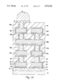
- FIG. 13 if desired, the structure shown in FIG. 12 is ready for conventional polyimide deposition and polishing for planarization.
- more levels of conductors and reference planes can be fabricated by repeating the above-described sequence of operations.
- copper bases 28a can be x-lines
- copper bases 28b can be y-lines
- copper base 28c is an additional reference plane with interconnecting pillars 32a, 32b, and 32c, all enclosed in a polyimide enclosure 40.
- the process sequence described in this invention is repeated to fabricate a high-density multilayer interconnect.
- bonding pads 42 and barrier/adhesion layer 41 can be fabricated as is conventional to form bonding pad for component bonding to the interconnect.
- a nickel alloy is described herein as suitable for electrically conductive layer 24, electrically conductive metal pillar 32, and protective overcoat 34. Acceptable compositions of these nickel alloys will be well known to those having skill in the art.
- suitable nickel alloys include nickel-phosphor, nickel-tungsten, nickel-platium, and nickel-chromium.
Abstract
Description
Claims (18)
Priority Applications (2)
| Application Number | Priority Date | Filing Date | Title |
|---|---|---|---|
| US07/426,619 US5071518A (en) | 1989-10-24 | 1989-10-24 | Method of making an electrical multilayer interconnect |
| US07/543,317 US5011580A (en) | 1989-10-24 | 1990-06-25 | Method of reworking an electrical multilayer interconnect |
Applications Claiming Priority (1)
| Application Number | Priority Date | Filing Date | Title |
|---|---|---|---|
| US07/426,619 US5071518A (en) | 1989-10-24 | 1989-10-24 | Method of making an electrical multilayer interconnect |
Related Child Applications (1)
| Application Number | Title | Priority Date | Filing Date |
|---|---|---|---|
| US07/543,317 Continuation-In-Part US5011580A (en) | 1989-10-24 | 1990-06-25 | Method of reworking an electrical multilayer interconnect |
Publications (1)
| Publication Number | Publication Date |
|---|---|
| US5071518A true US5071518A (en) | 1991-12-10 |
Family
ID=23691531
Family Applications (1)
| Application Number | Title | Priority Date | Filing Date |
|---|---|---|---|
| US07/426,619 Expired - Lifetime US5071518A (en) | 1989-10-24 | 1989-10-24 | Method of making an electrical multilayer interconnect |
Country Status (1)
| Country | Link |
|---|---|
| US (1) | US5071518A (en) |
Cited By (64)
| Publication number | Priority date | Publication date | Assignee | Title |
|---|---|---|---|---|
| US5118385A (en) * | 1991-05-28 | 1992-06-02 | Microelectronics And Computer Technology Corporation | Multilayer electrical interconnect fabrication with few process steps |
| US5142828A (en) * | 1990-06-25 | 1992-09-01 | Microelectronics And Computer Technology Corporation | Correcting a defective metallization layer on an electronic component by polishing |
| US5346858A (en) * | 1992-07-16 | 1994-09-13 | Texas Instruments Incorporated | Semiconductor non-corrosive metal overcoat |
| US5480835A (en) * | 1993-05-06 | 1996-01-02 | Motorola, Inc. | Electrical interconnect and method for forming the same |
| US5545927A (en) * | 1995-05-12 | 1996-08-13 | International Business Machines Corporation | Capped copper electrical interconnects |
| US5549808A (en) * | 1995-05-12 | 1996-08-27 | International Business Machines Corporation | Method for forming capped copper electrical interconnects |
| US5593919A (en) * | 1995-09-05 | 1997-01-14 | Motorola Inc. | Process for forming a semiconductor device including conductive members |
| US5670420A (en) * | 1994-12-05 | 1997-09-23 | Hyundai Electronics Industries Co., Ltd. | Method of forming metal interconnection layer of semiconductor device |
| US5827775A (en) * | 1993-09-10 | 1998-10-27 | Raytheon Comapny | Phase mask laser fabrication of fine pattern electronic interconnect structures |
| US5830805A (en) * | 1996-11-18 | 1998-11-03 | Cornell Research Foundation | Electroless deposition equipment or apparatus and method of performing electroless deposition |
| US5966634A (en) * | 1996-03-25 | 1999-10-12 | Kabushiki Kaisha Toshiba | Method of manufacturing semiconductor device having multi-layer wiring structure with diffusion preventing film |
| US6037248A (en) * | 1997-06-13 | 2000-03-14 | Micron Technology, Inc. | Method of fabricating integrated circuit wiring with low RC time delay |
| US6048445A (en) * | 1998-03-24 | 2000-04-11 | Intel Corporation | Method of forming a metal line utilizing electroplating |
| US6080656A (en) * | 1999-09-01 | 2000-06-27 | Taiwan Semiconductor Manufacturing Company | Method for forming a self-aligned copper structure with improved planarity |
| US6083375A (en) * | 1998-11-02 | 2000-07-04 | International Business Machines Corporation | Process for producing corrosion-resistant terminal metal pads for thin film packages |
| US6096648A (en) * | 1999-01-26 | 2000-08-01 | Amd | Copper/low dielectric interconnect formation with reduced electromigration |
| US6123825A (en) * | 1998-12-02 | 2000-09-26 | International Business Machines Corporation | Electromigration-resistant copper microstructure and process of making |
| US6126806A (en) * | 1998-12-02 | 2000-10-03 | International Business Machines Corporation | Enhancing copper electromigration resistance with indium and oxygen lamination |
| US6147408A (en) * | 1997-09-18 | 2000-11-14 | Ebara Corporation | Method of forming embedded copper interconnections and embedded copper interconnection structure |
| US6165912A (en) * | 1998-09-17 | 2000-12-26 | Cfmt, Inc. | Electroless metal deposition of electronic components in an enclosable vessel |
| US6181012B1 (en) * | 1998-04-27 | 2001-01-30 | International Business Machines Corporation | Copper interconnection structure incorporating a metal seed layer |
| US6180505B1 (en) | 1999-01-07 | 2001-01-30 | International Business Machines Corporation | Process for forming a copper-containing film |
| US6236101B1 (en) | 1997-11-05 | 2001-05-22 | Texas Instruments Incorporated | Metallization outside protective overcoat for improved capacitors and inductors |
| US6258707B1 (en) | 1999-01-07 | 2001-07-10 | International Business Machines Corporation | Triple damascence tungsten-copper interconnect structure |
| WO2001080303A2 (en) * | 2000-04-18 | 2001-10-25 | Motorola, Inc. | Method and apparatus for manufacturing an interconnect structure |
| US6350364B1 (en) | 2000-02-18 | 2002-02-26 | Taiwan Semiconductor Manufacturing Company | Method for improvement of planarity of electroplated copper |
| US6391754B1 (en) * | 1996-09-27 | 2002-05-21 | Texas Instruments Incorporated | Method of making an integrated circuit interconnect |
| US6428942B1 (en) | 1999-10-28 | 2002-08-06 | Fujitsu Limited | Multilayer circuit structure build up method |
| US20020150838A1 (en) * | 1999-10-28 | 2002-10-17 | Lei Zhang | Structure and method for forming a multilayered structure |
| US20020155661A1 (en) * | 1999-10-28 | 2002-10-24 | Massingill Thomas J. | Multi-chip module and method for forming and method for deplating defective capacitors |
| US6506668B1 (en) | 2001-06-22 | 2003-01-14 | Advanced Micro Devices, Inc. | Utilization of annealing enhanced or repaired seed layer to improve copper interconnect reliability |
| US6551924B1 (en) | 1999-11-02 | 2003-04-22 | International Business Machines Corporation | Post metalization chem-mech polishing dielectric etch |
| US6566242B1 (en) | 2001-03-23 | 2003-05-20 | International Business Machines Corporation | Dual damascene copper interconnect to a damascene tungsten wiring level |
| US20030127743A1 (en) * | 2001-11-30 | 2003-07-10 | Axel Brintzinger | Interconnect on a substrate |
| US20030169939A1 (en) * | 2002-01-04 | 2003-09-11 | Medlock Joel D. | Apparatus and method for Fast Hadamard Transforms |
| US20040219738A1 (en) * | 2000-08-22 | 2004-11-04 | Dinesh Chopra | Method of providing a structure using self-aligned features |
| US20050023697A1 (en) * | 2000-01-18 | 2005-02-03 | Micron Technology, Inc. | Methods for making integrated-circuit wiring from copper, silver, gold, and other metals |
| US20050116351A1 (en) * | 2003-07-14 | 2005-06-02 | Kirby Kyle K. | Semiconductor interconnect having conductive spring contacts |
| US7067421B2 (en) | 2000-05-31 | 2006-06-27 | Micron Technology, Inc. | Multilevel copper interconnect with double passivation |
| US7262505B2 (en) | 2000-01-18 | 2007-08-28 | Micron Technology, Inc. | Selective electroless-plated copper metallization |
| US7285196B2 (en) | 2000-01-18 | 2007-10-23 | Micron Technology, Inc. | Methods and apparatus for making integrated-circuit wiring from copper, silver, gold, and other metals |
| US7301190B2 (en) | 2000-01-18 | 2007-11-27 | Micron Technology, Inc. | Structures and methods to enhance copper metallization |
| US7358116B2 (en) * | 2002-04-29 | 2008-04-15 | Intel Corporation | Substrate conductive post formation |
| US20080200022A1 (en) * | 2007-02-15 | 2008-08-21 | John Callahan | Post-seed deposition process |
| US20080220608A1 (en) * | 2004-10-14 | 2008-09-11 | International Business Machines Corporation | Modified via bottom structure for reliability enhancement |
| EP1992207A1 (en) * | 2006-03-03 | 2008-11-19 | Wavenics Inc. | Multi-layer package structure and fabrication method thereof |
| US20090261473A1 (en) * | 2001-03-05 | 2009-10-22 | Megica Corporation | Low fabrication cost, fine pitch and high reliability solder bump |
| US20090267213A1 (en) * | 2001-03-05 | 2009-10-29 | Megica Corporation | Structure and manufacturing method of a chip scale package with low fabrication cost, fine pitch and high reliability solder bump |
| US20090288858A1 (en) * | 2008-05-23 | 2009-11-26 | Unimicron Technology Corp. | Circuit structure and manufacturing method thereof |
| US7960270B2 (en) | 2002-01-07 | 2011-06-14 | Megica Corporation | Method for fabricating circuit component |
| US20110193218A1 (en) * | 2010-02-05 | 2011-08-11 | International Business Machines Corporation | Solder Interconnect with Non-Wettable Sidewall Pillars and Methods of Manufacture |
| US8021921B2 (en) | 2002-10-25 | 2011-09-20 | Megica Corporation | Method of joining chips utilizing copper pillar |
| US8021976B2 (en) | 2002-10-15 | 2011-09-20 | Megica Corporation | Method of wire bonding over active area of a semiconductor circuit |
| US8067837B2 (en) | 2004-09-20 | 2011-11-29 | Megica Corporation | Metallization structure over passivation layer for IC chip |
| US8178967B2 (en) | 2001-09-17 | 2012-05-15 | Megica Corporation | Low fabrication cost, high performance, high reliability chip scale package |
| CN102469701A (en) * | 2010-11-09 | 2012-05-23 | 无锡江南计算技术研究所 | Manufacturing method of interconnection structure |
| EP2496062A1 (en) * | 2007-06-11 | 2012-09-05 | PPG Industries Ohio, Inc. | Method of forming solid blind vias through the dielectric coating on high density interconnect (HDI) substrate materials |
| US8294279B2 (en) | 2005-01-25 | 2012-10-23 | Megica Corporation | Chip package with dam bar restricting flow of underfill |
| US8481418B2 (en) | 2002-05-01 | 2013-07-09 | Megica Corporation | Low fabrication cost, high performance, high reliability chip scale package |
| US8518818B2 (en) * | 2011-09-16 | 2013-08-27 | Taiwan Semiconductor Manufacturing Co., Ltd. | Reverse damascene process |
| US8901733B2 (en) | 2001-02-15 | 2014-12-02 | Qualcomm Incorporated | Reliable metal bumps on top of I/O pads after removal of test probe marks |
| US9273409B2 (en) | 2001-03-30 | 2016-03-01 | Uri Cohen | Electroplated metallic conductors |
| US10060036B2 (en) * | 2015-12-04 | 2018-08-28 | National Chung-Shan Institute Of Science And Technology | Plated-layer structure for improving interface stress between aluminium nitride substrate and copper-plated layer |
| US11272623B2 (en) * | 2017-06-07 | 2022-03-08 | Ngk Spark Plug Co., Ltd. | Wiring substrate and method for producing wiring substrate |
Citations (9)
| Publication number | Priority date | Publication date | Assignee | Title |
|---|---|---|---|---|
| US3745094A (en) * | 1971-03-26 | 1973-07-10 | Ibm | Two resist method for printed circuit structure |
| US3791858A (en) * | 1971-12-13 | 1974-02-12 | Ibm | Method of forming multi-layer circuit panels |
| US4082591A (en) * | 1976-03-15 | 1978-04-04 | Mitsui-Anaconda Electro Copper Sheet Co., Ltd. | Surface treatment process for copper foil |
| US4159222A (en) * | 1977-01-11 | 1979-06-26 | Pactel Corporation | Method of manufacturing high density fine line printed circuitry |
| US4190474A (en) * | 1977-12-22 | 1980-02-26 | Gould Inc. | Method of making a printed circuit board having mutually etchable copper and nickel layers |
| US4233344A (en) * | 1978-07-20 | 1980-11-11 | Learonal, Inc. | Method of improving the adhesion of electroless metal deposits employing colloidal copper activator |
| US4306925A (en) * | 1977-01-11 | 1981-12-22 | Pactel Corporation | Method of manufacturing high density printed circuit |
| US4409037A (en) * | 1982-04-05 | 1983-10-11 | Macdermid Incorporated | Adhesion promoter for printed circuits |
| US4810332A (en) * | 1988-07-21 | 1989-03-07 | Microelectronics And Computer Technology Corporation | Method of making an electrical multilayer copper interconnect |
-
1989
- 1989-10-24 US US07/426,619 patent/US5071518A/en not_active Expired - Lifetime
Patent Citations (9)
| Publication number | Priority date | Publication date | Assignee | Title |
|---|---|---|---|---|
| US3745094A (en) * | 1971-03-26 | 1973-07-10 | Ibm | Two resist method for printed circuit structure |
| US3791858A (en) * | 1971-12-13 | 1974-02-12 | Ibm | Method of forming multi-layer circuit panels |
| US4082591A (en) * | 1976-03-15 | 1978-04-04 | Mitsui-Anaconda Electro Copper Sheet Co., Ltd. | Surface treatment process for copper foil |
| US4159222A (en) * | 1977-01-11 | 1979-06-26 | Pactel Corporation | Method of manufacturing high density fine line printed circuitry |
| US4306925A (en) * | 1977-01-11 | 1981-12-22 | Pactel Corporation | Method of manufacturing high density printed circuit |
| US4190474A (en) * | 1977-12-22 | 1980-02-26 | Gould Inc. | Method of making a printed circuit board having mutually etchable copper and nickel layers |
| US4233344A (en) * | 1978-07-20 | 1980-11-11 | Learonal, Inc. | Method of improving the adhesion of electroless metal deposits employing colloidal copper activator |
| US4409037A (en) * | 1982-04-05 | 1983-10-11 | Macdermid Incorporated | Adhesion promoter for printed circuits |
| US4810332A (en) * | 1988-07-21 | 1989-03-07 | Microelectronics And Computer Technology Corporation | Method of making an electrical multilayer copper interconnect |
Non-Patent Citations (8)
| Title |
|---|
| Jensen et al.., "Copper/Polyimide Materials for High Performance Packaging", IEEE Transactions on Components, Hybrids, and Manufacturing Technology, vol. CHMT-7, No. 4, Dec. 1984, pp. 384-393. |
| Jensen et al.., Copper/Polyimide Materials for High Performance Packaging , IEEE Transactions on Components, Hybrids, and Manufacturing Technology, vol. CHMT 7, No. 4, Dec. 1984, pp. 384 393. * |
| Lebow, "High Density/High Speed Multi-Chip Packaging", Proceedings of the Technical Conference, Sixth Annual International Electronics Packaging Conference, Nov. 1986, pp. 417-423. |
| Lebow, High Density/High Speed Multi Chip Packaging , Proceedings of the Technical Conference, Sixth Annual International Electronics Packaging Conference, Nov. 1986, pp. 417 423. * |
| Pan et al., "A Planar Approach to High Density Copper-Polyimide Interconnect Fabrication", Proceedings of the Technical Conference-Eighth Annual International Electronics Packaging Conference, Dallas TX, Nov. 7, 1988. |
| Pan et al., A Planar Approach to High Density Copper Polyimide Interconnect Fabrication , Proceedings of the Technical Conference Eighth Annual International Electronics Packaging Conference, Dallas TX, Nov. 7, 1988. * |
| Taylor et al., "The Wafer Transmission Module-Wafer Scale Integrated Packaging", IEEE 1985 Custom Integrated Circuits Conference, 1985, pp. 55-58. |
| Taylor et al., The Wafer Transmission Module Wafer Scale Integrated Packaging , IEEE 1985 Custom Integrated Circuits Conference, 1985, pp. 55 58. * |
Cited By (129)
| Publication number | Priority date | Publication date | Assignee | Title |
|---|---|---|---|---|
| US5142828A (en) * | 1990-06-25 | 1992-09-01 | Microelectronics And Computer Technology Corporation | Correcting a defective metallization layer on an electronic component by polishing |
| US5118385A (en) * | 1991-05-28 | 1992-06-02 | Microelectronics And Computer Technology Corporation | Multilayer electrical interconnect fabrication with few process steps |
| US5346858A (en) * | 1992-07-16 | 1994-09-13 | Texas Instruments Incorporated | Semiconductor non-corrosive metal overcoat |
| US5480835A (en) * | 1993-05-06 | 1996-01-02 | Motorola, Inc. | Electrical interconnect and method for forming the same |
| US5827775A (en) * | 1993-09-10 | 1998-10-27 | Raytheon Comapny | Phase mask laser fabrication of fine pattern electronic interconnect structures |
| US5670420A (en) * | 1994-12-05 | 1997-09-23 | Hyundai Electronics Industries Co., Ltd. | Method of forming metal interconnection layer of semiconductor device |
| US5549808A (en) * | 1995-05-12 | 1996-08-27 | International Business Machines Corporation | Method for forming capped copper electrical interconnects |
| US5705857A (en) * | 1995-05-12 | 1998-01-06 | International Business Machines Corporation | Capped copper electrical interconnects |
| US5545927A (en) * | 1995-05-12 | 1996-08-13 | International Business Machines Corporation | Capped copper electrical interconnects |
| US5898222A (en) * | 1995-05-12 | 1999-04-27 | International Business Machines Corporation | Capped copper electrical interconnects |
| US5593919A (en) * | 1995-09-05 | 1997-01-14 | Motorola Inc. | Process for forming a semiconductor device including conductive members |
| US5966634A (en) * | 1996-03-25 | 1999-10-12 | Kabushiki Kaisha Toshiba | Method of manufacturing semiconductor device having multi-layer wiring structure with diffusion preventing film |
| US6391754B1 (en) * | 1996-09-27 | 2002-05-21 | Texas Instruments Incorporated | Method of making an integrated circuit interconnect |
| US5830805A (en) * | 1996-11-18 | 1998-11-03 | Cornell Research Foundation | Electroless deposition equipment or apparatus and method of performing electroless deposition |
| US6037248A (en) * | 1997-06-13 | 2000-03-14 | Micron Technology, Inc. | Method of fabricating integrated circuit wiring with low RC time delay |
| US7271085B2 (en) | 1997-06-13 | 2007-09-18 | Micron Technology, Inc. | Method of fabricating a semiconductor interconnect structure |
| US20040038522A1 (en) * | 1997-06-13 | 2004-02-26 | Ahn Kie Y. | Method of fabricating a semiconductor interconnect structure |
| US6633074B2 (en) | 1997-06-13 | 2003-10-14 | Micron Technology, Inc. | Integrated circuit wiring with low RC time delay |
| US6787467B2 (en) | 1997-09-18 | 2004-09-07 | Ebara Corporation | Method of forming embedded copper interconnections and embedded copper interconnection structure |
| US6391775B1 (en) | 1997-09-18 | 2002-05-21 | Ebara Corporation | Method of forming embedded copper interconnections and embedded copper interconnection structure |
| US6147408A (en) * | 1997-09-18 | 2000-11-14 | Ebara Corporation | Method of forming embedded copper interconnections and embedded copper interconnection structure |
| US6236101B1 (en) | 1997-11-05 | 2001-05-22 | Texas Instruments Incorporated | Metallization outside protective overcoat for improved capacitors and inductors |
| US6284617B1 (en) | 1997-11-05 | 2001-09-04 | Texas Instruments Incorporated | Metalization outside protective overcoat for improved capacitors and inductors |
| US6048445A (en) * | 1998-03-24 | 2000-04-11 | Intel Corporation | Method of forming a metal line utilizing electroplating |
| US6181012B1 (en) * | 1998-04-27 | 2001-01-30 | International Business Machines Corporation | Copper interconnection structure incorporating a metal seed layer |
| US6399496B1 (en) | 1998-04-27 | 2002-06-04 | International Business Machines Corporation | Copper interconnection structure incorporating a metal seed layer |
| US6165912A (en) * | 1998-09-17 | 2000-12-26 | Cfmt, Inc. | Electroless metal deposition of electronic components in an enclosable vessel |
| US6235412B1 (en) | 1998-11-02 | 2001-05-22 | International Business Machines Corporation | Corrosion-resistant terminal metal pads for thin film packages |
| US6083375A (en) * | 1998-11-02 | 2000-07-04 | International Business Machines Corporation | Process for producing corrosion-resistant terminal metal pads for thin film packages |
| US6126806A (en) * | 1998-12-02 | 2000-10-03 | International Business Machines Corporation | Enhancing copper electromigration resistance with indium and oxygen lamination |
| US6235406B1 (en) | 1998-12-02 | 2001-05-22 | International Business Machines Corporation | Copper film including laminated impurities |
| US6123825A (en) * | 1998-12-02 | 2000-09-26 | International Business Machines Corporation | Electromigration-resistant copper microstructure and process of making |
| US6572982B1 (en) | 1998-12-02 | 2003-06-03 | International Business Machines Corporation | Electromigration-resistant copper microstructure |
| US8138079B2 (en) | 1998-12-21 | 2012-03-20 | Megica Corporation | Method of wire bonding over active area of a semiconductor circuit |
| US6258707B1 (en) | 1999-01-07 | 2001-07-10 | International Business Machines Corporation | Triple damascence tungsten-copper interconnect structure |
| US6274935B2 (en) | 1999-01-07 | 2001-08-14 | International Business Machines Corporation | Copper wire-bonding pad |
| US6180505B1 (en) | 1999-01-07 | 2001-01-30 | International Business Machines Corporation | Process for forming a copper-containing film |
| US6096648A (en) * | 1999-01-26 | 2000-08-01 | Amd | Copper/low dielectric interconnect formation with reduced electromigration |
| US6080656A (en) * | 1999-09-01 | 2000-06-27 | Taiwan Semiconductor Manufacturing Company | Method for forming a self-aligned copper structure with improved planarity |
| US20020155661A1 (en) * | 1999-10-28 | 2002-10-24 | Massingill Thomas J. | Multi-chip module and method for forming and method for deplating defective capacitors |
| US20020119396A1 (en) * | 1999-10-28 | 2002-08-29 | Jiang Hunt Hang | Structure and method for forming z-laminated multilayered packaging substrate |
| US6882045B2 (en) | 1999-10-28 | 2005-04-19 | Thomas J. Massingill | Multi-chip module and method for forming and method for deplating defective capacitors |
| US6869750B2 (en) | 1999-10-28 | 2005-03-22 | Fujitsu Limited | Structure and method for forming a multilayered structure |
| US20020150838A1 (en) * | 1999-10-28 | 2002-10-17 | Lei Zhang | Structure and method for forming a multilayered structure |
| US6428942B1 (en) | 1999-10-28 | 2002-08-06 | Fujitsu Limited | Multilayer circuit structure build up method |
| US6551924B1 (en) | 1999-11-02 | 2003-04-22 | International Business Machines Corporation | Post metalization chem-mech polishing dielectric etch |
| US7301190B2 (en) | 2000-01-18 | 2007-11-27 | Micron Technology, Inc. | Structures and methods to enhance copper metallization |
| US7253521B2 (en) * | 2000-01-18 | 2007-08-07 | Micron Technology, Inc. | Methods for making integrated-circuit wiring from copper, silver, gold, and other metals |
| US8779596B2 (en) | 2000-01-18 | 2014-07-15 | Micron Technology, Inc. | Structures and methods to enhance copper metallization |
| US7368378B2 (en) | 2000-01-18 | 2008-05-06 | Micron Technology, Inc. | Methods for making integrated-circuit wiring from copper, silver, gold, and other metals |
| US7378737B2 (en) | 2000-01-18 | 2008-05-27 | Micron Technology, Inc. | Structures and methods to enhance copper metallization |
| US7285196B2 (en) | 2000-01-18 | 2007-10-23 | Micron Technology, Inc. | Methods and apparatus for making integrated-circuit wiring from copper, silver, gold, and other metals |
| US20050023697A1 (en) * | 2000-01-18 | 2005-02-03 | Micron Technology, Inc. | Methods for making integrated-circuit wiring from copper, silver, gold, and other metals |
| US7402516B2 (en) | 2000-01-18 | 2008-07-22 | Micron Technology, Inc. | Method for making integrated circuits |
| US7535103B2 (en) | 2000-01-18 | 2009-05-19 | Micron Technology, Inc. | Structures and methods to enhance copper metallization |
| US7670469B2 (en) | 2000-01-18 | 2010-03-02 | Micron Technology, Inc. | Methods and apparatus for making integrated-circuit wiring from copper, silver, gold, and other metals |
| US7262505B2 (en) | 2000-01-18 | 2007-08-28 | Micron Technology, Inc. | Selective electroless-plated copper metallization |
| US7262130B1 (en) | 2000-01-18 | 2007-08-28 | Micron Technology, Inc. | Methods for making integrated-circuit wiring from copper, silver, gold, and other metals |
| US6350364B1 (en) | 2000-02-18 | 2002-02-26 | Taiwan Semiconductor Manufacturing Company | Method for improvement of planarity of electroplated copper |
| KR100818902B1 (en) * | 2000-04-18 | 2008-04-04 | 프리스케일 세미컨덕터, 인크. | Method and apparatus for manufacturing an interconnect structure |
| WO2001080303A3 (en) * | 2000-04-18 | 2002-02-21 | Motorola Inc | Method and apparatus for manufacturing an interconnect structure |
| US6429531B1 (en) | 2000-04-18 | 2002-08-06 | Motorola, Inc. | Method and apparatus for manufacturing an interconnect structure |
| WO2001080303A2 (en) * | 2000-04-18 | 2001-10-25 | Motorola, Inc. | Method and apparatus for manufacturing an interconnect structure |
| US7067421B2 (en) | 2000-05-31 | 2006-06-27 | Micron Technology, Inc. | Multilevel copper interconnect with double passivation |
| US20040219738A1 (en) * | 2000-08-22 | 2004-11-04 | Dinesh Chopra | Method of providing a structure using self-aligned features |
| US7109112B2 (en) | 2000-08-22 | 2006-09-19 | Micron Technology, Inc. | Method of providing a structure using self-aligned features |
| US20060154483A1 (en) * | 2000-08-22 | 2006-07-13 | Micron Technology, Inc. | Method of providing a structure using self-aligned features |
| US8901733B2 (en) | 2001-02-15 | 2014-12-02 | Qualcomm Incorporated | Reliable metal bumps on top of I/O pads after removal of test probe marks |
| US7863739B2 (en) | 2001-03-05 | 2011-01-04 | Megica Corporation | Low fabrication cost, fine pitch and high reliability solder bump |
| US8072070B2 (en) | 2001-03-05 | 2011-12-06 | Megica Corporation | Low fabrication cost, fine pitch and high reliability solder bump |
| US20090267213A1 (en) * | 2001-03-05 | 2009-10-29 | Megica Corporation | Structure and manufacturing method of a chip scale package with low fabrication cost, fine pitch and high reliability solder bump |
| US8158508B2 (en) | 2001-03-05 | 2012-04-17 | Megica Corporation | Structure and manufacturing method of a chip scale package |
| US20090261473A1 (en) * | 2001-03-05 | 2009-10-22 | Megica Corporation | Low fabrication cost, fine pitch and high reliability solder bump |
| US8368213B2 (en) | 2001-03-05 | 2013-02-05 | Megica Corporation | Low fabrication cost, fine pitch and high reliability solder bump |
| US7902679B2 (en) | 2001-03-05 | 2011-03-08 | Megica Corporation | Structure and manufacturing method of a chip scale package with low fabrication cost, fine pitch and high reliability solder bump |
| US20030232494A1 (en) * | 2001-03-23 | 2003-12-18 | Adams Charlotte D. | Dual damascene copper interconnect to a damascene tungsten wiring level |
| US7230336B2 (en) | 2001-03-23 | 2007-06-12 | International Business Machines Corporation | Dual damascene copper interconnect to a damascene tungsten wiring level |
| US6566242B1 (en) | 2001-03-23 | 2003-05-20 | International Business Machines Corporation | Dual damascene copper interconnect to a damascene tungsten wiring level |
| US9530653B2 (en) | 2001-03-30 | 2016-12-27 | Uri Cohen | High speed electroplating metallic conductors |
| US9273409B2 (en) | 2001-03-30 | 2016-03-01 | Uri Cohen | Electroplated metallic conductors |
| US6506668B1 (en) | 2001-06-22 | 2003-01-14 | Advanced Micro Devices, Inc. | Utilization of annealing enhanced or repaired seed layer to improve copper interconnect reliability |
| US9369175B2 (en) | 2001-09-17 | 2016-06-14 | Qualcomm Incorporated | Low fabrication cost, high performance, high reliability chip scale package |
| US8178967B2 (en) | 2001-09-17 | 2012-05-15 | Megica Corporation | Low fabrication cost, high performance, high reliability chip scale package |
| US20030127743A1 (en) * | 2001-11-30 | 2003-07-10 | Axel Brintzinger | Interconnect on a substrate |
| US6943101B2 (en) * | 2001-11-30 | 2005-09-13 | Infineon Technologies Ag | Manufacturing of a corrosion protected interconnect on a substrate |
| KR100753006B1 (en) * | 2001-11-30 | 2007-08-30 | 인피니온 테크놀로지스 아게 | Fabrication method for an interconnect on a substrate and a corresponding interconnect |
| US20030169939A1 (en) * | 2002-01-04 | 2003-09-11 | Medlock Joel D. | Apparatus and method for Fast Hadamard Transforms |
| US7960270B2 (en) | 2002-01-07 | 2011-06-14 | Megica Corporation | Method for fabricating circuit component |
| US8461679B2 (en) | 2002-01-07 | 2013-06-11 | Megica Corporation | Method for fabricating circuit component |
| US8890336B2 (en) | 2002-01-07 | 2014-11-18 | Qualcomm Incorporated | Cylindrical bonding structure and method of manufacture |
| US7358116B2 (en) * | 2002-04-29 | 2008-04-15 | Intel Corporation | Substrate conductive post formation |
| US8481418B2 (en) | 2002-05-01 | 2013-07-09 | Megica Corporation | Low fabrication cost, high performance, high reliability chip scale package |
| US8742580B2 (en) | 2002-10-15 | 2014-06-03 | Megit Acquisition Corp. | Method of wire bonding over active area of a semiconductor circuit |
| US9153555B2 (en) | 2002-10-15 | 2015-10-06 | Qualcomm Incorporated | Method of wire bonding over active area of a semiconductor circuit |
| US8021976B2 (en) | 2002-10-15 | 2011-09-20 | Megica Corporation | Method of wire bonding over active area of a semiconductor circuit |
| US8026588B2 (en) | 2002-10-15 | 2011-09-27 | Megica Corporation | Method of wire bonding over active area of a semiconductor circuit |
| US9142527B2 (en) | 2002-10-15 | 2015-09-22 | Qualcomm Incorporated | Method of wire bonding over active area of a semiconductor circuit |
| US8421222B2 (en) | 2002-10-25 | 2013-04-16 | Megica Corporation | Chip package having a chip combined with a substrate via a copper pillar |
| US8021921B2 (en) | 2002-10-25 | 2011-09-20 | Megica Corporation | Method of joining chips utilizing copper pillar |
| US7391117B2 (en) | 2003-07-14 | 2008-06-24 | Micron Technology, Inc. | Method for fabricating semiconductor components with conductive spring contacts |
| US20060125106A1 (en) * | 2003-07-14 | 2006-06-15 | Kirby Kyle K | Method for fabricating semiconductor components with conductive spring contacts |
| US20060125107A1 (en) * | 2003-07-14 | 2006-06-15 | Kirby Kyle K | Test system for semiconductor components having conductive spring contacts |
| US20050116351A1 (en) * | 2003-07-14 | 2005-06-02 | Kirby Kyle K. | Semiconductor interconnect having conductive spring contacts |
| US7314821B2 (en) | 2003-07-14 | 2008-01-01 | Micron Technology, Inc. | Method for fabricating a semiconductor interconnect having conductive spring contacts |
| US7411304B2 (en) * | 2003-07-14 | 2008-08-12 | Micron Technology, Inc. | Semiconductor interconnect having conductive spring contacts |
| US7449910B2 (en) | 2003-07-14 | 2008-11-11 | Micron Technology, Inc. | Test system for semiconductor components having conductive spring contacts |
| US8742582B2 (en) | 2004-09-20 | 2014-06-03 | Megit Acquisition Corp. | Solder interconnect on IC chip |
| US8067837B2 (en) | 2004-09-20 | 2011-11-29 | Megica Corporation | Metallization structure over passivation layer for IC chip |
| US7906428B2 (en) | 2004-10-14 | 2011-03-15 | International Business Machines Corporation | Modified via bottom structure for reliability enhancement |
| US20080220608A1 (en) * | 2004-10-14 | 2008-09-11 | International Business Machines Corporation | Modified via bottom structure for reliability enhancement |
| US8294279B2 (en) | 2005-01-25 | 2012-10-23 | Megica Corporation | Chip package with dam bar restricting flow of underfill |
| EP1992207A4 (en) * | 2006-03-03 | 2010-11-17 | Wavenics Inc | Multi-layer package structure and fabrication method thereof |
| EP1992207A1 (en) * | 2006-03-03 | 2008-11-19 | Wavenics Inc. | Multi-layer package structure and fabrication method thereof |
| US20090175022A1 (en) * | 2006-03-03 | 2009-07-09 | Wavenics Inc. | Multi-layer package structure and fabrication method thereof |
| US7598163B2 (en) | 2007-02-15 | 2009-10-06 | John Callahan | Post-seed deposition process |
| US20080200022A1 (en) * | 2007-02-15 | 2008-08-21 | John Callahan | Post-seed deposition process |
| EP2496062A1 (en) * | 2007-06-11 | 2012-09-05 | PPG Industries Ohio, Inc. | Method of forming solid blind vias through the dielectric coating on high density interconnect (HDI) substrate materials |
| US20090288858A1 (en) * | 2008-05-23 | 2009-11-26 | Unimicron Technology Corp. | Circuit structure and manufacturing method thereof |
| US8186049B2 (en) | 2008-05-23 | 2012-05-29 | Unimicron Technology Corp. | Method of making a circuit structure |
| US20110193218A1 (en) * | 2010-02-05 | 2011-08-11 | International Business Machines Corporation | Solder Interconnect with Non-Wettable Sidewall Pillars and Methods of Manufacture |
| US9018760B2 (en) | 2010-02-05 | 2015-04-28 | International Business Machines Corporation | Solder interconnect with non-wettable sidewall pillars and methods of manufacture |
| US8637392B2 (en) | 2010-02-05 | 2014-01-28 | International Business Machines Corporation | Solder interconnect with non-wettable sidewall pillars and methods of manufacture |
| CN102469701B (en) * | 2010-11-09 | 2013-06-12 | 无锡江南计算技术研究所 | Manufacturing method of interconnection structure |
| CN102469701A (en) * | 2010-11-09 | 2012-05-23 | 无锡江南计算技术研究所 | Manufacturing method of interconnection structure |
| US8518818B2 (en) * | 2011-09-16 | 2013-08-27 | Taiwan Semiconductor Manufacturing Co., Ltd. | Reverse damascene process |
| US9536834B2 (en) | 2011-09-16 | 2017-01-03 | Taiwan Semiconductor Manufacturing Co., Ltd. | Reverse damascene process |
| US9607946B2 (en) | 2011-09-16 | 2017-03-28 | Taiwan Semiconductor Manufacturing Co., Ltd. | Reverse damascene process |
| US10060036B2 (en) * | 2015-12-04 | 2018-08-28 | National Chung-Shan Institute Of Science And Technology | Plated-layer structure for improving interface stress between aluminium nitride substrate and copper-plated layer |
| US11272623B2 (en) * | 2017-06-07 | 2022-03-08 | Ngk Spark Plug Co., Ltd. | Wiring substrate and method for producing wiring substrate |
Similar Documents
| Publication | Publication Date | Title |
|---|---|---|
| US5071518A (en) | Method of making an electrical multilayer interconnect | |
| US5011580A (en) | Method of reworking an electrical multilayer interconnect | |
| US4810332A (en) | Method of making an electrical multilayer copper interconnect | |
| US4899439A (en) | Method of fabricating a high density electrical interconnect | |
| JP3486184B2 (en) | Chip carrier substrate | |
| US5116463A (en) | Detecting completion of electroless via fill | |
| EP1087648B1 (en) | Multi-purpose finish for printed wiring boards and method of manufacture of such boards | |
| US5897368A (en) | Method of fabricating metallized vias with steep walls | |
| US4285780A (en) | Method of making a multi-level circuit board | |
| US4752555A (en) | Method of manufacturing multilayer circuit board | |
| US5164332A (en) | Diffusion barrier for copper features | |
| US5268068A (en) | High aspect ratio molybdenum composite mask method | |
| US20060030147A1 (en) | Selectively coating bond pads | |
| US6370768B1 (en) | Circuit board, a method for manufacturing same, and a method of electroless plating | |
| KR950034679A (en) | Multilayer Circuit Device and Manufacturing Method Thereof | |
| EP0445759A1 (en) | Multilayer structures with layer interconnection | |
| US5830533A (en) | Selective patterning of metallization on a dielectric substrate | |
| US4628149A (en) | Substrate having a pattern of an alloy of gold and a noble and a base metal with the pattern isolated by oxides of the noble and the base metals | |
| JPS6032311B2 (en) | Electric conductor and its manufacturing method | |
| US20020140105A1 (en) | High strength vias | |
| US5196089A (en) | Multilayer ceramic substrate for mounting of semiconductor device | |
| US5208656A (en) | Multilayer wiring substrate and production thereof | |
| WO1998040910A1 (en) | Wiring forming method for semiconductor device and semiconductor device | |
| US3679472A (en) | Method for bonding a metal pattern to a substrate | |
| TW200410615A (en) | Method of forming conductor wiring pattern |
Legal Events
| Date | Code | Title | Description |
|---|---|---|---|
| AS | Assignment |
Owner name: MICROELECTRONICS AND COMPUTER TECHNOLOGY CORPORATI Free format text: ASSIGNMENT OF ASSIGNORS INTEREST.;ASSIGNOR:PAN, JU-DON T.;REEL/FRAME:005168/0081 Effective date: 19891023 |
|
| STCF | Information on status: patent grant |
Free format text: PATENTED CASE |
|
| FEPP | Fee payment procedure |
Free format text: PAYOR NUMBER ASSIGNED (ORIGINAL EVENT CODE: ASPN); ENTITY STATUS OF PATENT OWNER: LARGE ENTITY |
|
| FPAY | Fee payment |
Year of fee payment: 4 |
|
| SULP | Surcharge for late payment | ||
| REMI | Maintenance fee reminder mailed | ||
| FPAY | Fee payment |
Year of fee payment: 8 |
|
| REMI | Maintenance fee reminder mailed | ||
| FPAY | Fee payment |
Year of fee payment: 12 |
|
| SULP | Surcharge for late payment |
Year of fee payment: 11 |
|
| AS | Assignment |
Owner name: STOVOKOR TECHNOLOGY LLC, CALIFORNIA Free format text: ASSIGNMENT OF ASSIGNORS INTEREST;ASSIGNOR:MICROLECTRONICS AND COMPUTER TECHNOLOGY CORPORATION;REEL/FRAME:014892/0165 Effective date: 20040128 |
|
| FEPP | Fee payment procedure |
Free format text: PAYOR NUMBER ASSIGNED (ORIGINAL EVENT CODE: ASPN); ENTITY STATUS OF PATENT OWNER: LARGE ENTITY Free format text: PAYER NUMBER DE-ASSIGNED (ORIGINAL EVENT CODE: RMPN); ENTITY STATUS OF PATENT OWNER: LARGE ENTITY |