US5077693A - Dynamic random access memory - Google Patents
Dynamic random access memory Download PDFInfo
- Publication number
- US5077693A US5077693A US07/563,167 US56316790A US5077693A US 5077693 A US5077693 A US 5077693A US 56316790 A US56316790 A US 56316790A US 5077693 A US5077693 A US 5077693A
- Authority
- US
- United States
- Prior art keywords
- signal
- column
- state
- row
- coupled
- Prior art date
- Legal status (The legal status is an assumption and is not a legal conclusion. Google has not performed a legal analysis and makes no representation as to the accuracy of the status listed.)
- Expired - Lifetime
Links
Images


Classifications
-
- G—PHYSICS
- G11—INFORMATION STORAGE
- G11C—STATIC STORES
- G11C11/00—Digital stores characterised by the use of particular electric or magnetic storage elements; Storage elements therefor
- G11C11/21—Digital stores characterised by the use of particular electric or magnetic storage elements; Storage elements therefor using electric elements
- G11C11/34—Digital stores characterised by the use of particular electric or magnetic storage elements; Storage elements therefor using electric elements using semiconductor devices
- G11C11/40—Digital stores characterised by the use of particular electric or magnetic storage elements; Storage elements therefor using electric elements using semiconductor devices using transistors
- G11C11/401—Digital stores characterised by the use of particular electric or magnetic storage elements; Storage elements therefor using electric elements using semiconductor devices using transistors forming cells needing refreshing or charge regeneration, i.e. dynamic cells
- G11C11/4063—Auxiliary circuits, e.g. for addressing, decoding, driving, writing, sensing or timing
- G11C11/407—Auxiliary circuits, e.g. for addressing, decoding, driving, writing, sensing or timing for memory cells of the field-effect type
- G11C11/4076—Timing circuits
Definitions
- the present invention relates, in general, to dynamic random access memories (DRAMs) and, more particularly, to a DRAM having synchronized control timing.
- DRAMs dynamic random access memories
- DRAMs are known in the industry. Access to the DRAM (reading and writing information) is generally controlled by a DRAM Controller. When access is to be made, the controller sends a Row Address Strobe (RAS) and a Column Address Strobe (CAS) to select the particular bit that is to be accessed. The timing of the controller output is based on the input from a system clock.
- RAS Row Address Strobe
- CAS Column Address Strobe
- a system clock which is used to clock the processor and other peripheral circuitry which in turn generate the necessary timing signals for the memory system. Since the timing signals to the DRAM are processed through other logic devices prior to reaching the DRAM, the resulting signals will have delays (skews) with respect to other signals and the system clock. Further, these skews will be different for each signal since the signals are processed through different circuitry. Because of these skews, designers must allow for extra time in the signal lengths. The result of having to add 6-8 ns to a 40 ns signal is quite substantial.
- Another object of the present invention is to reduce the skew associated with the row and column address strobes (RAS and CAS).
- Still another object of the present invention is to provide a DRAM having synchronized control timing.
- Yet another object of the present invention is to provide a DRAM having control timing synchronized with a clock input.
- a particular embodiment of the present invention consists of a DRAM having a clock input, a column enable, and a row enable.
- the DRAM is accessed and row and column addresses are latched based on the clock input.
- FIG. 1 is a block diagram of a prior art DRAM
- FIG. 2 is a timing diagram of the prior art DRAM of FIG. 1;
- FIG. 3 is a block diagram of DRAM embodying the present invention.
- FIG'S 4A-4E are circuit diagrams of the registers and control logic of FIG. 3.
- FIG'S 5-10 are timing diagrams of the DRAM of FIG. 3.
- DRAM 10 consists of a memory array 11 which is comprised of a matrix of memory cells.
- a bit line sense amplifier and input/output gating circuit 12 is a series of sense amplifiers coupled between a bit line pair of memory array 11 and an input/output line pair to amplify the memory cell output.
- Row and column decoders 13 and 14, respectively, are coupled to memory array 11 to decode the row and column address of the cell being accessed
- Row and column address buffers 15 and 16, respectively, are coupled to the address input lines (A0-A8) and to row and column decoders 13 and 14. Buffers serve to store the address signals.
- First and second clock generators 17 and 18 are coupled to the Row Access Strobe (RAS) and Column Access Strobe (CAS) inputs. These inputs control the operation of the clocks which in turn control the operation of the row and column buffers and decoders (13-16).
- RAS Row Access Strobe
- CAS Column Access Strobe
- a refresh controller/counter 20 is provided to refresh the memory array 11.
- Data In and Data Out buffers 21 and 22 are provided to store data that is being written to or read from memory array 11. Buffers 21 and 22 are controlled by a write enable (W), through an AND gate 23 and an output enable (G).
- a substrate bias generator 25 is provided coupled to a power line (V CC ) and ground (V SS ).
- FIG. 2 a timing diagram for the prior art DRAM of FIG. 1.
- FIG. 2 illustrates timing lines for RAS, CAS, the address, and the data output.
- the timing figures are as follows:
- the system clock drives the processor which provides control signals to the DRAM controller which in turn generates the RAS and CAS signals.
- the processing of these signals through the various circuitry results in skews which must be accounted for by the system designer. This results in a memory system that is not operating as fast as the DRAM data sheet indicates.
- FIG. 3 a block diagram of a DRAM, generally designated 30, embodying the present invention is illustrated.
- the same numbers as used in FIG. 1 are used to designate like components.
- the main difference between FIGS. 1 and 3 is the use of row and column enables, RE and CE, in place of RAS and CAS, and a system clock input (CK).
- RE and CE in place of RAS and CAS
- CK system clock input
- further registers and control logic 31 are provided.
- FIG. 4A illustrates a clock buffer 40 which receives the external clock signal (CK) and generates internal trap (CLK/CLKB) and latch (CKPUL/CKPULB) signals.
- the input buffer of clock chain 40 is a TTL compatible ratioed inverter which is enabled by a clock enable (CKENB) signal.
- the clock enable signal is a power-down option which reduces standby current and chip noise generated by the external clock.
- FIG. 4B illustrates an RE latch 42 which, in a synchronized mode, will replace the RAS buffer.
- Latch 42 consists of a TTL compatible ratioed inverter and two inverter-latches.
- CLK and CLKB signals When the external clock goes high, the CLK and CLKB signals will trap the data in the first inverter-latch to meet setup and hold specs. Subsequently, the CKPUL and CKPULB pulses are generated to allow trapped data to be stored in the second inverter-latch.
- FIG'S 4C and 4D, CE and W latches 43 and 44 are illustrated. As shown, latches 43 and 44 are similar to latch 42 except for the input signal.
- FIG. 4E illustrates a modified column address buffer 45 in which is a pair of N-channel pass devices and capacitors have been added to the column address buffers.
- the pass transistors are "on" when the external clock and CE are low to allow new column addresses to be loaded. This will initiate the CE chain.
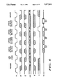
- the timing diagram associated with DRAM 30 is illustrated in FIG. 5.
- the reading and latching of row and column addresses is accomplished on the clock signal.
- the rising edge of the clock signal is used.
- the active cycle begins with RE being low and remaining low for a hold time after CK goes high. This is equivalent to the RAS going low for the standard DRAM.
- the row addresses are latched on the first occurrence of RE being low during a rising edge of a clock signal.
- CE is set low during a subsequent rising edge of the CK signal
- the column address is latched into the column address buffer. If W was low, then a write operation is performed. If W was high during this CK signal, then a read operation occurs and data-out will become valid an access time later.
- CE is set high on the subsequent rising edge of the CK signal, then the page cycle is extended as if the CK edge did not occur. If W remains high during this time, then a fast page mode read is conducted. This is illustrated in the timing diagram of FIG. 6. After a precharge, the row address is latched in on the first rising edge. Next, the first column address is latched in and the memory cell corresponding to that row and column address is read. In the next clock cycle, RE remains low and CE is low, but a different column address is provided. This new column address is latched and the data for that memory cell is read. This process can continue until RE goes high.
- FIG. 7 a fast page mode read-modify-write cycle is illustrated. Following a precharge, the row address is latched in on the first rising edge of the CK pulse. Next, the first column address is latched and the memory cell corresponding to that row and column address is accessed. Since the first step is to read, W must be high on this CK. Following the read, CE goes high and W goes low. This keeps the same column address latched in the column address buffers and causes a write to occur into this address. This can be repeated for other column addresses on the same page. During the read portion, G is kept low and during the write portion G is high allowing data in and out of the data buffers.
- a variation of the example in FIG. 7 is a fast page mode read/write cycle illustrated in FIG. 8.
- the main difference is that the column being written to does not have to be the came as the column just read. This is accomplished by keeping CE low while W is toggled between read and write. Since CE is low, the address is locked into the column address buffer on each CK. Then, depending on the state of W, data is either read out of or written to the appropriate memory cell to the data buffers. The G signal then regulates the flow of data from the data buffers to a data bus.
- the precharge shown at the beginning of the cycles illustrated in FIGS. 6-8 is initiated with RE high on a rising CK edge. If CE is also high on this transition, the outputs will be tri-stated. If CE is low then the outputs will remain valid.
- the precharge may be extended by keeping RE high on subsequent rising CK edges. A new active cycle will begin upon the first occurrence of RE low in a rising CK edge.
- CAS before RAS refresh cycle there is a refresh cycle referred to as CAS before RAS refresh cycle. This can also be performed in the present invention as illustrated in FIG. 9. If both RE and CE are low on the first CK edge after precharge, then the refresh cycle will be started. This refresh cycle will continue as long as RE remains low.
- FIG. 10 Another method of refreshing the memory is referred to as a hidden refresh cycle, illustrated in FIG. 10. This occurs when, at the end of a read cycle, RE goes high while CE stays low. At this point, a precharge is conducted. Then, when RE goes low again, both RE and CE are low putting the system into a refresh cycle.
- One potential disadvantage to the present invention is the added power due to the CK input toggling.
- One way in which this drawback can be minimized is to inhibit, or power-down, the CK input. This would occur by powering down the CK signal when RE is high at the beginning of a precharge. The CK would then stay low until RE goes low.
- the present invention provides a DRAM having synchronized control timing for reducing the skew associated with the row and column address strobes.
Abstract
Description
______________________________________
SIGNAL    DESCRIPTION      MIN    MAX
______________________________________
 t.sub.RCD
           ##STR1##         20 ns  50 ns
t.sub.ASR Row Address Setup
                            0 ns  --
t.sub.RAH Row Address Hold 10 ns  --
t.sub.ASC Column Address Setup
                            0 ns  --
t.sub.CAH Column Address Hold
                           15 ns  --
 t.sub.RAC
           ##STR2##         --     70 ns
 t.sub.CAC
           ##STR3##         --     20 ns
______________________________________
Claims (13)
Priority Applications (1)
| Application Number | Priority Date | Filing Date | Title |
|---|---|---|---|
| US07/563,167 US5077693A (en) | 1990-08-06 | 1990-08-06 | Dynamic random access memory |
Applications Claiming Priority (1)
| Application Number | Priority Date | Filing Date | Title |
|---|---|---|---|
| US07/563,167 US5077693A (en) | 1990-08-06 | 1990-08-06 | Dynamic random access memory |
Publications (1)
| Publication Number | Publication Date |
|---|---|
| US5077693A true US5077693A (en) | 1991-12-31 |
Family
ID=24249375
Family Applications (1)
| Application Number | Title | Priority Date | Filing Date |
|---|---|---|---|
| US07/563,167 Expired - Lifetime US5077693A (en) | 1990-08-06 | 1990-08-06 | Dynamic random access memory |
Country Status (1)
| Country | Link |
|---|---|
| US (1) | US5077693A (en) |
Cited By (45)
| Publication number | Priority date | Publication date | Assignee | Title |
|---|---|---|---|---|
| US5251181A (en) * | 1991-06-05 | 1993-10-05 | Kabushiki Kaisha Toshiba | Random access memory device and method of controlling same in pipe line page mode |
| US5287327A (en) * | 1990-11-20 | 1994-02-15 | Oki Electric Industry Co., Ltd. | Synchronous dynamic random access memory |
| US5379261A (en) * | 1993-03-26 | 1995-01-03 | United Memories, Inc. | Method and circuit for improved timing and noise margin in a DRAM |
| US5386385A (en) * | 1994-01-31 | 1995-01-31 | Texas Instruments Inc. | Method and apparatus for preventing invalid operating modes and an application to synchronous memory devices |
| US5390149A (en) * | 1991-04-23 | 1995-02-14 | Texas Instruments Incorporated | System including a data processor, a synchronous dram, a peripheral device, and a system clock |
| US5412615A (en) * | 1992-12-28 | 1995-05-02 | Fujitsu Limited | Semiconductor integrated circuit device |
| US5450364A (en) * | 1994-01-31 | 1995-09-12 | Texas Instruments Incorporated | Method and apparatus for production testing of self-refresh operations and a particular application to synchronous memory devices |
| US5485430A (en) * | 1992-12-22 | 1996-01-16 | Sgs-Thomson Microelectronics, Inc. | Multiple clocked dynamic sense amplifier |
| US5513327A (en) * | 1990-04-18 | 1996-04-30 | Rambus, Inc. | Integrated circuit I/O using a high performance bus interface |
| US5517459A (en) * | 1993-11-16 | 1996-05-14 | Mitsubishi Denki Kabushiki Kaisha | Semiconductor memory device in which data are read and written asynchronously with application of address signal |
| US5539696A (en) * | 1994-01-31 | 1996-07-23 | Patel; Vipul C. | Method and apparatus for writing data in a synchronous memory having column independent sections and a method and apparatus for performing write mask operations |
| US5577236A (en) * | 1994-12-30 | 1996-11-19 | International Business Machines Corporation | Memory controller for reading data from synchronous RAM |
| US5610874A (en) * | 1993-11-08 | 1997-03-11 | Samsung Electronics Co., Ltd. | Fast burst-mode synchronous random access memory device |
| US5630096A (en) * | 1995-05-10 | 1997-05-13 | Microunity Systems Engineering, Inc. | Controller for a synchronous DRAM that maximizes throughput by allowing memory requests and commands to be issued out of order |
| US5666324A (en) * | 1996-03-15 | 1997-09-09 | Mitsubishi Denki Kabushiki Kaisha | Clock synchronous semiconductor memory device having current consumption reduced |
| USRE35680E (en) * | 1988-11-29 | 1997-12-02 | Matsushita Electric Industrial Co., Ltd. | Dynamic video RAM incorporating on chip vector/image mode line modification |
| USRE35921E (en) * | 1988-11-29 | 1998-10-13 | Matsushita Electric Industrial Co., Ltd. | Dynamic video RAM incorporating single clock random port control |
| US5835956A (en) * | 1899-10-02 | 1998-11-10 | Samsung Electronics Co., Ltd. | Synchronous dram having a plurality of latency modes |
| US5867448A (en) * | 1997-06-11 | 1999-02-02 | Cypress Semiconductor Corp. | Buffer for memory modules with trace delay compensation |
| US5890196A (en) * | 1996-03-28 | 1999-03-30 | Motorola, Inc. | Method and apparatus for performing page mode accesses |
| US5953263A (en) * | 1997-02-10 | 1999-09-14 | Rambus Inc. | Synchronous memory device having a programmable register and method of controlling same |
| US5995443A (en) * | 1990-04-18 | 1999-11-30 | Rambus Inc. | Synchronous memory device |
| US6094380A (en) * | 1997-12-31 | 2000-07-25 | Kim; Jung Pill | Memory device with a data output buffer and the control method thereof |
| US6115321A (en) * | 1997-06-17 | 2000-09-05 | Texas Instruments Incorporated | Synchronous dynamic random access memory with four-bit data prefetch |
| US6192003B1 (en) | 1998-11-30 | 2001-02-20 | Matsushita Electric Industrial Co., Ltd. | Semiconductor memory device using a relatively low-speed clock frequency and capable of latching a row address and a column address with one clock signal and performing a page operation |
| US6209071B1 (en) | 1996-05-07 | 2001-03-27 | Rambus Inc. | Asynchronous request/synchronous data dynamic random access memory |
| US6212596B1 (en) | 1991-10-24 | 2001-04-03 | Texas Instruments Incorporated | Synchronous memory and data processing system having a programmable burst length |
| US6240047B1 (en) | 1998-07-06 | 2001-05-29 | Texas Instruments Incorporated | Synchronous dynamic random access memory with four-bit data prefetch |
| US6279116B1 (en) | 1992-10-02 | 2001-08-21 | Samsung Electronics Co., Ltd. | Synchronous dynamic random access memory devices that utilize clock masking signals to control internal clock signal generation |
| US20020087790A1 (en) * | 1995-10-19 | 2002-07-04 | Barth Richard Maurice | Memory integrated circuit device which samples data upon detection of a strobe signal |
| US20020087777A1 (en) * | 1990-04-18 | 2002-07-04 | Michael Farmwald | Synchronous integrated circuit device |
| US6493789B2 (en) | 1995-10-19 | 2002-12-10 | Rambus Inc. | Memory device which receives write masking and automatic precharge information |
| US20030018880A1 (en) * | 1987-12-14 | 2003-01-23 | Daniel Litaize | Multiple-mode memory system |
| US6591353B1 (en) | 1995-10-19 | 2003-07-08 | Rambus Inc. | Protocol for communication with dynamic memory |
| US20050235066A1 (en) * | 2004-04-19 | 2005-10-20 | Nokia Corporation | Addressing data within dynamic random access memory |
| US7177998B2 (en) | 2001-04-24 | 2007-02-13 | Rambus Inc. | Method, system and memory controller utilizing adjustable read data delay settings |
| US7197611B2 (en) | 1997-10-10 | 2007-03-27 | Rambus Inc. | Integrated circuit memory device having write latency function |
| US20070201298A1 (en) * | 2006-02-27 | 2007-08-30 | Freescale Semiconductor, Inc. | Bit line precharge in embedded memory |
| US7301831B2 (en) | 2004-09-15 | 2007-11-27 | Rambus Inc. | Memory systems with variable delays for write data signals |
| US20070280030A1 (en) * | 2006-05-23 | 2007-12-06 | Freescale Semiconductor, Inc. | Contention-free hierarchical bit line in embedded memory and method thereof |
| US7437527B2 (en) | 1997-10-10 | 2008-10-14 | Rambus Inc. | Memory device with delayed issuance of internal write command |
| US20090122619A1 (en) * | 1992-01-22 | 2009-05-14 | Purple Mountain Server Llc | Enhanced DRAM with Embedded Registers |
| US8238470B2 (en) | 1997-06-20 | 2012-08-07 | Massachusetts Institute Of Technology | Digital transmitter |
| US8248884B2 (en) | 1997-10-10 | 2012-08-21 | Rambus Inc. | Method of controlling a memory device having multiple power modes |
| US8320202B2 (en) | 2001-04-24 | 2012-11-27 | Rambus Inc. | Clocked memory system with termination component |
Citations (7)
| Publication number | Priority date | Publication date | Assignee | Title |
|---|---|---|---|---|
| US4649511A (en) * | 1983-07-25 | 1987-03-10 | General Electric Company | Dynamic memory controller for single-chip microprocessor |
| US4710902A (en) * | 1985-10-04 | 1987-12-01 | Motorola, Inc. | Technique restore for a dynamic random access memory |
| US4734880A (en) * | 1983-04-12 | 1988-03-29 | Sony Corporation | Dynamic random access memory arrangements having WE, RAS, and CAS derived from a single system clock |
| US4740921A (en) * | 1985-10-04 | 1988-04-26 | Motorola, Inc. | Precharge of a dram data line to an intermediate voltage |
| US4754425A (en) * | 1985-10-18 | 1988-06-28 | Gte Communication Systems Corporation | Dynamic random access memory refresh circuit selectively adapted to different clock frequencies |
| US4823322A (en) * | 1986-11-29 | 1989-04-18 | Mitsubishi Denki Kabushiki Kaisha | Dynamic random access memory device having an improved timing arrangement |
| US4831597A (en) * | 1986-11-25 | 1989-05-16 | Kabushiki Kaisha Toshiba | Dynamic random access semiconductor memory wherein the RAS and CAS strobes respectively select the bit line and word line pairs |
-
1990
- 1990-08-06 US US07/563,167 patent/US5077693A/en not_active Expired - Lifetime
Patent Citations (7)
| Publication number | Priority date | Publication date | Assignee | Title |
|---|---|---|---|---|
| US4734880A (en) * | 1983-04-12 | 1988-03-29 | Sony Corporation | Dynamic random access memory arrangements having WE, RAS, and CAS derived from a single system clock |
| US4649511A (en) * | 1983-07-25 | 1987-03-10 | General Electric Company | Dynamic memory controller for single-chip microprocessor |
| US4710902A (en) * | 1985-10-04 | 1987-12-01 | Motorola, Inc. | Technique restore for a dynamic random access memory |
| US4740921A (en) * | 1985-10-04 | 1988-04-26 | Motorola, Inc. | Precharge of a dram data line to an intermediate voltage |
| US4754425A (en) * | 1985-10-18 | 1988-06-28 | Gte Communication Systems Corporation | Dynamic random access memory refresh circuit selectively adapted to different clock frequencies |
| US4831597A (en) * | 1986-11-25 | 1989-05-16 | Kabushiki Kaisha Toshiba | Dynamic random access semiconductor memory wherein the RAS and CAS strobes respectively select the bit line and word line pairs |
| US4823322A (en) * | 1986-11-29 | 1989-04-18 | Mitsubishi Denki Kabushiki Kaisha | Dynamic random access memory device having an improved timing arrangement |
Non-Patent Citations (1)
| Title |
|---|
| Motorola Semiconductor Technical Data, MCM514256A, 1988. * |
Cited By (162)
| Publication number | Priority date | Publication date | Assignee | Title |
|---|---|---|---|---|
| US5835956A (en) * | 1899-10-02 | 1998-11-10 | Samsung Electronics Co., Ltd. | Synchronous dram having a plurality of latency modes |
| US7136971B2 (en) | 1987-12-14 | 2006-11-14 | Intel Corporation | Memory controller for synchronous burst transfers |
| US20040139285A1 (en) * | 1987-12-14 | 2004-07-15 | Intel Corporation | Memory component with multiple transfer formats |
| US20030120895A1 (en) * | 1987-12-14 | 2003-06-26 | Daniel Litaize | Memory controller for synchronous burst transfers |
| US20030018880A1 (en) * | 1987-12-14 | 2003-01-23 | Daniel Litaize | Multiple-mode memory system |
| USRE35680E (en) * | 1988-11-29 | 1997-12-02 | Matsushita Electric Industrial Co., Ltd. | Dynamic video RAM incorporating on chip vector/image mode line modification |
| USRE35921E (en) * | 1988-11-29 | 1998-10-13 | Matsushita Electric Industrial Co., Ltd. | Dynamic video RAM incorporating single clock random port control |
| US6715020B2 (en) | 1990-04-18 | 2004-03-30 | Rambus Inc. | Synchronous integrated circuit device |
| US6728819B2 (en) | 1990-04-18 | 2004-04-27 | Rambus Inc. | Synchronous memory device |
| US6564281B2 (en) | 1990-04-18 | 2003-05-13 | Rambus Inc. | Synchronous memory device having automatic precharge |
| US5513327A (en) * | 1990-04-18 | 1996-04-30 | Rambus, Inc. | Integrated circuit I/O using a high performance bus interface |
| US6546446B2 (en) | 1990-04-18 | 2003-04-08 | Rambus Inc. | Synchronous memory device having automatic precharge |
| US20020087777A1 (en) * | 1990-04-18 | 2002-07-04 | Michael Farmwald | Synchronous integrated circuit device |
| US6415339B1 (en) | 1990-04-18 | 2002-07-02 | Rambus Inc. | Memory device having a plurality of programmable internal registers and a delay time register |
| US6598171B1 (en) | 1990-04-18 | 2003-07-22 | Rambus Inc. | Integrated circuit I/O using a high performance bus interface |
| US6304937B1 (en) | 1990-04-18 | 2001-10-16 | Rambus Inc. | Method of operation of a memory controller |
| US6260097B1 (en) | 1990-04-18 | 2001-07-10 | Rambus | Method and apparatus for controlling a synchronous memory device |
| US6185644B1 (en) | 1990-04-18 | 2001-02-06 | Rambus Inc. | Memory system including a plurality of memory devices and a transceiver device |
| US6128696A (en) * | 1990-04-18 | 2000-10-03 | Rambus Inc. | Synchronous memory device utilizing request protocol and method of operation of same |
| US6182184B1 (en) | 1990-04-18 | 2001-01-30 | Rambus Inc. | Method of operating a memory device having a variable data input length |
| US6085284A (en) * | 1990-04-18 | 2000-07-04 | Rambus Inc. | Method of operating a memory device having a variable data output length and an identification register |
| US5809263A (en) | 1990-04-18 | 1998-09-15 | Rambus Inc. | Integrated circuit I/O using a high performance bus interface |
| US6070222A (en) * | 1990-04-18 | 2000-05-30 | Rambus Inc. | Synchronous memory device having identification register |
| US6044426A (en) * | 1990-04-18 | 2000-03-28 | Rambus Inc. | Memory system having memory devices each including a programmable internal register |
| US6038195A (en) * | 1990-04-18 | 2000-03-14 | Rambus Inc. | Synchronous memory device having a delay time register and method of operating same |
| US6034918A (en) * | 1990-04-18 | 2000-03-07 | Rambus Inc. | Method of operating a memory having a variable data output length and a programmable register |
| US5841715A (en) * | 1990-04-18 | 1998-11-24 | Rambus, Inc. | Integrated circuit I/O using high performance bus interface |
| US5841580A (en) * | 1990-04-18 | 1998-11-24 | Rambus, Inc. | Integrated circuit I/O using a high performance bus interface |
| US6035365A (en) * | 1990-04-18 | 2000-03-07 | Rambus Inc. | Dual clocked synchronous memory device having a delay time register and method of operating same |
| US6032214A (en) * | 1990-04-18 | 2000-02-29 | Rambus Inc. | Method of operating a synchronous memory device having a variable data output length |
| US6032215A (en) * | 1990-04-18 | 2000-02-29 | Rambus Inc. | Synchronous memory device utilizing two external clocks |
| US5915105A (en) | 1990-04-18 | 1999-06-22 | Rambus Inc. | Integrated circuit I/O using a high performance bus interface |
| US5928343A (en) | 1990-04-18 | 1999-07-27 | Rambus Inc. | Memory module having memory devices containing internal device ID registers and method of initializing same |
| US5995443A (en) * | 1990-04-18 | 1999-11-30 | Rambus Inc. | Synchronous memory device |
| US5430688A (en) * | 1990-11-20 | 1995-07-04 | Oki Electric Industry Co., Ltd. | Synchronous dynamic random access memory |
| US5521879A (en) * | 1990-11-20 | 1996-05-28 | Oki Electric Industry Co., Ltd. | Synchronous dynamic random acess memory |
| US5339276A (en) * | 1990-11-20 | 1994-08-16 | Oki Electric Industry Co., Ltd. | Synchronous dynamic random access memory |
| US5287327A (en) * | 1990-11-20 | 1994-02-15 | Oki Electric Industry Co., Ltd. | Synchronous dynamic random access memory |
| US5587954A (en) * | 1991-04-23 | 1996-12-24 | Texas Instruments Incorporated | Random access memory arranged for operating synchronously with a microprocessor and a system including a data processor, a synchronous DRAM, a peripheral device, and a system clock |
| US5982694A (en) * | 1991-04-23 | 1999-11-09 | Texas Instruments Incorporated | High speed memory arranged for operating synchronously with a microprocessor |
| US5390149A (en) * | 1991-04-23 | 1995-02-14 | Texas Instruments Incorporated | System including a data processor, a synchronous dram, a peripheral device, and a system clock |
| US5808958A (en) * | 1991-04-23 | 1998-09-15 | Texas Instruments Incorporated | Random access memory with latency arranged for operating synchronously with a micro processor and a system including a data processor, a synchronous DRAM, a peripheral device, and a system clock |
| US5251181A (en) * | 1991-06-05 | 1993-10-05 | Kabushiki Kaisha Toshiba | Random access memory device and method of controlling same in pipe line page mode |
| US6230250B1 (en) | 1991-10-24 | 2001-05-08 | Texas Instruments Incorporated | Synchronous memory and data processing system having a programmable burst order |
| US6212596B1 (en) | 1991-10-24 | 2001-04-03 | Texas Instruments Incorporated | Synchronous memory and data processing system having a programmable burst length |
| US6223264B1 (en) | 1991-10-24 | 2001-04-24 | Texas Instruments Incorporated | Synchronous dynamic random access memory and data processing system using an address select signal |
| US20090122619A1 (en) * | 1992-01-22 | 2009-05-14 | Purple Mountain Server Llc | Enhanced DRAM with Embedded Registers |
| US6438063B1 (en) | 1992-10-02 | 2002-08-20 | Samsung Electronics Co., Ltd. | Integrated circuit memory devices having selectable column addressing and methods of operating same |
| US6343036B1 (en) | 1992-10-02 | 2002-01-29 | Samsung Electronics Co., Ltd. | Multi-bank dynamic random access memory devices having all bank precharge capability |
| US6279116B1 (en) | 1992-10-02 | 2001-08-21 | Samsung Electronics Co., Ltd. | Synchronous dynamic random access memory devices that utilize clock masking signals to control internal clock signal generation |
| US5838990A (en) * | 1992-10-02 | 1998-11-17 | Samsung Electronics Co., Ltd. | Circuit in a semiconductor memory for programming operation modes of the memory |
| US5485430A (en) * | 1992-12-22 | 1996-01-16 | Sgs-Thomson Microelectronics, Inc. | Multiple clocked dynamic sense amplifier |
| US5412615A (en) * | 1992-12-28 | 1995-05-02 | Fujitsu Limited | Semiconductor integrated circuit device |
| US5379261A (en) * | 1993-03-26 | 1995-01-03 | United Memories, Inc. | Method and circuit for improved timing and noise margin in a DRAM |
| US5610874A (en) * | 1993-11-08 | 1997-03-11 | Samsung Electronics Co., Ltd. | Fast burst-mode synchronous random access memory device |
| US5517459A (en) * | 1993-11-16 | 1996-05-14 | Mitsubishi Denki Kabushiki Kaisha | Semiconductor memory device in which data are read and written asynchronously with application of address signal |
| US5841729A (en) * | 1993-11-16 | 1998-11-24 | Mitsubishi Denki Kabushiki Kaisha | Semiconductor memory device in which data are read and written asynchronously with application of address signal |
| US6222790B1 (en) * | 1993-11-16 | 2001-04-24 | Mitsubishi Denki Kabushiki Kaisha | Semiconductor memory device in which data are read and written asynchronously with application of address signal |
| US6768696B2 (en) | 1993-11-16 | 2004-07-27 | Renesas Technology Corp. | Semiconductor memory device in which data are read and written asynchronously with application of address signal |
| US20040017699A1 (en) * | 1993-11-16 | 2004-01-29 | Mitsubishi Denki Kabushiki Kaisha | Semiconductor memory device in which data are read and written asynchronously with application of address signal |
| US5691954A (en) * | 1993-11-16 | 1997-11-25 | Mitsubishi Denki Kabushiki Kaisha | Semiconductor memory device in which data are read and written asynchronously with application of address signal |
| US5386385A (en) * | 1994-01-31 | 1995-01-31 | Texas Instruments Inc. | Method and apparatus for preventing invalid operating modes and an application to synchronous memory devices |
| US5539696A (en) * | 1994-01-31 | 1996-07-23 | Patel; Vipul C. | Method and apparatus for writing data in a synchronous memory having column independent sections and a method and apparatus for performing write mask operations |
| US5450364A (en) * | 1994-01-31 | 1995-09-12 | Texas Instruments Incorporated | Method and apparatus for production testing of self-refresh operations and a particular application to synchronous memory devices |
| US5577236A (en) * | 1994-12-30 | 1996-11-19 | International Business Machines Corporation | Memory controller for reading data from synchronous RAM |
| US5630096A (en) * | 1995-05-10 | 1997-05-13 | Microunity Systems Engineering, Inc. | Controller for a synchronous DRAM that maximizes throughput by allowing memory requests and commands to be issued out of order |
| US6470405B2 (en) | 1995-10-19 | 2002-10-22 | Rambus Inc. | Protocol for communication with dynamic memory |
| US6496897B2 (en) | 1995-10-19 | 2002-12-17 | Rambus Inc. | Semiconductor memory device which receives write masking information |
| US6493789B2 (en) | 1995-10-19 | 2002-12-10 | Rambus Inc. | Memory device which receives write masking and automatic precharge information |
| US6810449B1 (en) | 1995-10-19 | 2004-10-26 | Rambus, Inc. | Protocol for communication with dynamic memory |
| US20020087790A1 (en) * | 1995-10-19 | 2002-07-04 | Barth Richard Maurice | Memory integrated circuit device which samples data upon detection of a strobe signal |
| US6681288B2 (en) | 1995-10-19 | 2004-01-20 | Rambus Inc. | Memory device with receives write masking information |
| US6931467B2 (en) | 1995-10-19 | 2005-08-16 | Rambus Inc. | Memory integrated circuit device which samples data upon detection of a strobe signal |
| US6591353B1 (en) | 1995-10-19 | 2003-07-08 | Rambus Inc. | Protocol for communication with dynamic memory |
| US5666324A (en) * | 1996-03-15 | 1997-09-09 | Mitsubishi Denki Kabushiki Kaisha | Clock synchronous semiconductor memory device having current consumption reduced |
| US5890196A (en) * | 1996-03-28 | 1999-03-30 | Motorola, Inc. | Method and apparatus for performing page mode accesses |
| US20070201280A1 (en) * | 1996-05-07 | 2007-08-30 | Rambus Inc. | Memory device |
| US20030061460A1 (en) * | 1996-05-07 | 2003-03-27 | Barth Richard Maurice | Asynchronous request/synchronous data dynamic random access memory |
| US6532522B1 (en) | 1996-05-07 | 2003-03-11 | Rambus Inc. | Asynchronous request/synchronous data dynamic random access memory |
| US6405296B1 (en) | 1996-05-07 | 2002-06-11 | Rambus Inc. | Asynchronous request/synchronous data dynamic random access memory |
| US6542976B2 (en) | 1996-05-07 | 2003-04-01 | Rambus Inc. | Memory device having an internal register |
| US7315929B2 (en) | 1996-05-07 | 2008-01-01 | Rambus Inc. | Memory device |
| US6209071B1 (en) | 1996-05-07 | 2001-03-27 | Rambus Inc. | Asynchronous request/synchronous data dynamic random access memory |
| US7085906B2 (en) | 1996-05-07 | 2006-08-01 | Rambus Inc. | Memory device |
| US5953263A (en) * | 1997-02-10 | 1999-09-14 | Rambus Inc. | Synchronous memory device having a programmable register and method of controlling same |
| US5867448A (en) * | 1997-06-11 | 1999-02-02 | Cypress Semiconductor Corp. | Buffer for memory modules with trace delay compensation |
| US6115321A (en) * | 1997-06-17 | 2000-09-05 | Texas Instruments Incorporated | Synchronous dynamic random access memory with four-bit data prefetch |
| US9647857B2 (en) | 1997-06-20 | 2017-05-09 | Massachusetts Institute Of Technology | Digital transmitter |
| US9419824B2 (en) | 1997-06-20 | 2016-08-16 | Massachusetts Institute Of Technology | Digital transmitter |
| US8989303B2 (en) | 1997-06-20 | 2015-03-24 | Massachusetts Institute Of Technology | Digital transmitter |
| US8238467B2 (en) | 1997-06-20 | 2012-08-07 | Massachusetts Institute Of Technology | Digital transmitter |
| US8923433B2 (en) | 1997-06-20 | 2014-12-30 | Massachusetts Institute Of Technology | Digital transmitter |
| US8761235B2 (en) | 1997-06-20 | 2014-06-24 | Massachusetts Institute Of Technology | Digital transmitter |
| US8681837B2 (en) | 1997-06-20 | 2014-03-25 | Massachusetts Institute Of Technology | Digital Transmitter |
| US8243847B2 (en) | 1997-06-20 | 2012-08-14 | Massachusetts Institute Of Technology | Digital transmitter |
| US8238470B2 (en) | 1997-06-20 | 2012-08-07 | Massachusetts Institute Of Technology | Digital transmitter |
| US8311147B2 (en) | 1997-06-20 | 2012-11-13 | Massachusetts Institute Of Technology | Digital transmitter |
| US8259841B2 (en) | 1997-06-20 | 2012-09-04 | Massachusetts Institute Of Technology | Digital transmitter |
| US8254491B2 (en) | 1997-06-20 | 2012-08-28 | Massachusetts Institute Of Technology | Digital transmitter |
| US8248884B2 (en) | 1997-10-10 | 2012-08-21 | Rambus Inc. | Method of controlling a memory device having multiple power modes |
| US8560797B2 (en) | 1997-10-10 | 2013-10-15 | Rambus Inc. | Method and apparatus for indicating mask information |
| US8305839B2 (en) | 1997-10-10 | 2012-11-06 | Rambus Inc. | Memory device having multiple power modes |
| US8504790B2 (en) | 1997-10-10 | 2013-08-06 | Rambus Inc. | Memory component having write operation with multiple time periods |
| US7330953B2 (en) | 1997-10-10 | 2008-02-12 | Rambus Inc. | Memory system having delayed write timing |
| US7330952B2 (en) | 1997-10-10 | 2008-02-12 | Rambus Inc. | Integrated circuit memory device having delayed write timing based on read response time |
| US7360050B2 (en) | 1997-10-10 | 2008-04-15 | Rambus Inc. | Integrated circuit memory device having delayed write capability |
| US7437527B2 (en) | 1997-10-10 | 2008-10-14 | Rambus Inc. | Memory device with delayed issuance of internal write command |
| US8205056B2 (en) | 1997-10-10 | 2012-06-19 | Rambus Inc. | Memory controller for controlling write signaling |
| US7287119B2 (en) | 1997-10-10 | 2007-10-23 | Rambus Inc. | Integrated circuit memory device with delayed write command processing |
| US7197611B2 (en) | 1997-10-10 | 2007-03-27 | Rambus Inc. | Integrated circuit memory device having write latency function |
| US7496709B2 (en) | 1997-10-10 | 2009-02-24 | Rambus Inc. | Integrated circuit memory device having delayed write timing based on read response time |
| US8140805B2 (en) | 1997-10-10 | 2012-03-20 | Rambus Inc. | Memory component having write operation with multiple time periods |
| US8019958B2 (en) | 1997-10-10 | 2011-09-13 | Rambus Inc. | Memory write signaling and methods thereof |
| US7793039B2 (en) | 1997-10-10 | 2010-09-07 | Rambus Inc. | Interface for a semiconductor memory device and method for controlling the interface |
| US7870357B2 (en) | 1997-10-10 | 2011-01-11 | Rambus Inc. | Memory system and method for two step memory write operations |
| US6094380A (en) * | 1997-12-31 | 2000-07-25 | Kim; Jung Pill | Memory device with a data output buffer and the control method thereof |
| US6240047B1 (en) | 1998-07-06 | 2001-05-29 | Texas Instruments Incorporated | Synchronous dynamic random access memory with four-bit data prefetch |
| US6192003B1 (en) | 1998-11-30 | 2001-02-20 | Matsushita Electric Industrial Co., Ltd. | Semiconductor memory device using a relatively low-speed clock frequency and capable of latching a row address and a column address with one clock signal and performing a page operation |
| US8214616B2 (en) | 2001-04-24 | 2012-07-03 | Rambus Inc. | Memory controller device having timing offset capability |
| US8625371B2 (en) | 2001-04-24 | 2014-01-07 | Rambus Inc. | Memory component with terminated and unterminated signaling inputs |
| US10706910B2 (en) | 2001-04-24 | 2020-07-07 | Rambus Inc. | Memory controller |
| US10236051B2 (en) | 2001-04-24 | 2019-03-19 | Rambus Inc. | Memory controller |
| US7484064B2 (en) | 2001-04-24 | 2009-01-27 | Rambus Inc. | Method and apparatus for signaling between devices of a memory system |
| US9741424B2 (en) | 2001-04-24 | 2017-08-22 | Rambus Inc. | Memory controller |
| US9472262B2 (en) | 2001-04-24 | 2016-10-18 | Rambus Inc. | Memory controller |
| US9311976B2 (en) | 2001-04-24 | 2016-04-12 | Rambus Inc. | Memory module |
| US9053778B2 (en) | 2001-04-24 | 2015-06-09 | Rambus Inc. | Memory controller that enforces strobe-to-strobe timing offset |
| US7177998B2 (en) | 2001-04-24 | 2007-02-13 | Rambus Inc. | Method, system and memory controller utilizing adjustable read data delay settings |
| US7200055B2 (en) | 2001-04-24 | 2007-04-03 | Rambus Inc. | Memory module with termination component |
| US8320202B2 (en) | 2001-04-24 | 2012-11-27 | Rambus Inc. | Clocked memory system with termination component |
| US8359445B2 (en) | 2001-04-24 | 2013-01-22 | Rambus Inc. | Method and apparatus for signaling between devices of a memory system |
| US8760944B2 (en) | 2001-04-24 | 2014-06-24 | Rambus Inc. | Memory component that samples command/address signals in response to both edges of a clock signal |
| US8391039B2 (en) | 2001-04-24 | 2013-03-05 | Rambus Inc. | Memory module with termination component |
| US8395951B2 (en) | 2001-04-24 | 2013-03-12 | Rambus Inc. | Memory controller |
| US8462566B2 (en) | 2001-04-24 | 2013-06-11 | Rambus Inc. | Memory module with termination component |
| US7209397B2 (en) | 2001-04-24 | 2007-04-24 | Rambus Inc. | Memory device with clock multiplier circuit |
| US7225311B2 (en) | 2001-04-24 | 2007-05-29 | Rambus Inc. | Method and apparatus for coordinating memory operations among diversely-located memory components |
| US8537601B2 (en) | 2001-04-24 | 2013-09-17 | Rambus Inc. | Memory controller with selective data transmission delay |
| US7225292B2 (en) | 2001-04-24 | 2007-05-29 | Rambus Inc. | Memory module with termination component |
| US8717837B2 (en) | 2001-04-24 | 2014-05-06 | Rambus Inc. | Memory module |
| US7210016B2 (en) | 2001-04-24 | 2007-04-24 | Rambus Inc. | Method, system and memory controller utilizing adjustable write data delay settings |
| US7142479B2 (en) * | 2004-04-19 | 2006-11-28 | Nokia Corporation | Addressing data within dynamic random access memory |
| US20050235066A1 (en) * | 2004-04-19 | 2005-10-20 | Nokia Corporation | Addressing data within dynamic random access memory |
| US7724590B2 (en) | 2004-09-15 | 2010-05-25 | Rambus Inc. | Memory controller with multiple delayed timing signals |
| US8045407B2 (en) | 2004-09-15 | 2011-10-25 | Rambus Inc. | Memory-write timing calibration including generation of multiple delayed timing signals |
| US11664067B2 (en) | 2004-09-15 | 2023-05-30 | Rambus Inc. | Memory system component that enables clock-to-strobe skew compensation |
| US11100976B2 (en) | 2004-09-15 | 2021-08-24 | Rambus Inc. | Memory controller with clock-to-strobe skew compensation |
| US7301831B2 (en) | 2004-09-15 | 2007-11-27 | Rambus Inc. | Memory systems with variable delays for write data signals |
| US9229470B2 (en) | 2004-09-15 | 2016-01-05 | Rambus Inc. | Memory controller with clock-to-strobe skew compensation |
| US10755764B2 (en) | 2004-09-15 | 2020-08-25 | Rambus Inc. | Memory component that enables calibrated command- and data-timing signal arrival |
| US8493802B1 (en) | 2004-09-15 | 2013-07-23 | Rambus Inc. | Memory controller having a write-timing calibration mode |
| US9437279B2 (en) | 2004-09-15 | 2016-09-06 | Rambus Inc. | Memory controller with clock-to-strobe skew compensation |
| US8218382B2 (en) | 2004-09-15 | 2012-07-10 | Rambus Inc. | Memory component having a write-timing calibration mode |
| US8743636B2 (en) | 2004-09-15 | 2014-06-03 | Rambus Inc. | Memory module having a write-timing calibration mode |
| US7480193B2 (en) | 2004-09-15 | 2009-01-20 | Rambus Inc. | Memory component with multiple delayed timing signals |
| US9830971B2 (en) | 2004-09-15 | 2017-11-28 | Rambus Inc. | Memory controller with clock-to-strobe skew compensation |
| US8363493B2 (en) | 2004-09-15 | 2013-01-29 | Rambus Inc. | Memory controller having a write-timing calibration mode |
| US10325645B2 (en) | 2004-09-15 | 2019-06-18 | Rambus Inc. | Memory controller with clock-to-strobe skew compensation |
| US7286423B2 (en) | 2006-02-27 | 2007-10-23 | Freescale Semiconductor, Inc. | Bit line precharge in embedded memory |
| US20070201298A1 (en) * | 2006-02-27 | 2007-08-30 | Freescale Semiconductor, Inc. | Bit line precharge in embedded memory |
| US7440335B2 (en) | 2006-05-23 | 2008-10-21 | Freescale Semiconductor, Inc. | Contention-free hierarchical bit line in embedded memory and method thereof |
| US20070280030A1 (en) * | 2006-05-23 | 2007-12-06 | Freescale Semiconductor, Inc. | Contention-free hierarchical bit line in embedded memory and method thereof |
Similar Documents
| Publication | Publication Date | Title |
|---|---|---|
| US5077693A (en) | Dynamic random access memory | |
| US6954384B2 (en) | Semiconductor device | |
| US6665231B2 (en) | Semiconductor device having pipelined dynamic memory | |
| US7212465B2 (en) | Clock signal generation apparatus for use in semiconductor memory device and its method | |
| US5999481A (en) | Method and apparatus for controlling the operation of an integrated circuit responsive to out-of-synchronism control signals | |
| JP2697633B2 (en) | Synchronous semiconductor memory device | |
| US6426915B2 (en) | Fast cycle RAM and data readout method therefor | |
| US5754481A (en) | Clock synchronous type DRAM with latch | |
| US20050141333A1 (en) | Latch circuit and synchronous memory including the same | |
| JP3341710B2 (en) | Semiconductor storage device | |
| US6456563B1 (en) | Semiconductor memory device that operates in sychronization with a clock signal | |
| JP3689229B2 (en) | Column selection line enable circuit for semiconductor memory device | |
| US6166993A (en) | Synchronous semiconductor memory device | |
| US6006290A (en) | System for performing high speed burst operation in memory device utilizing CAS clock to control and activate /WE and /OE control signals | |
| US6345007B1 (en) | Prefetch and restore method and apparatus of semiconductor memory device | |
| US7068550B2 (en) | 4-bit prefetch-type FCRAM having improved data write control circuit in memory cell array and method of masking data using the 4-bit prefetch-type FCRAM | |
| US5761137A (en) | DRAM access system and method | |
| JP4060527B2 (en) | Clock synchronous dynamic memory | |
| US5663912A (en) | Semiconductor memory device | |
| US5923610A (en) | Timing scheme for memory arrays | |
| JPH04229482A (en) | Dram memory-system |
Legal Events
| Date | Code | Title | Description |
|---|---|---|---|
| AS | Assignment |
Owner name: MOTOROLA INC., A CORP. OF DE, ILLINOIS Free format text: ASSIGNMENT OF ASSIGNORS INTEREST.;ASSIGNORS:HARDEE, KIM C.;CHAPMAN, DAVID B.;REEL/FRAME:005402/0831 Effective date: 19900719 |
|
| STCF | Information on status: patent grant |
Free format text: PATENTED CASE |
|
| AS | Assignment |
Owner name: APPLE COMPUTER, INC., CALIFORNIA Free format text: ASSIGNMENT OF ASSIGNORS INTEREST.;ASSIGNOR:PINEDA, JUAN;REEL/FRAME:006135/0734 Effective date: 19920512 |
|
| FEPP | Fee payment procedure |
Free format text: PAYOR NUMBER ASSIGNED (ORIGINAL EVENT CODE: ASPN); ENTITY STATUS OF PATENT OWNER: LARGE ENTITY |
|
| FEPP | Fee payment procedure |
Free format text: PAYOR NUMBER ASSIGNED (ORIGINAL EVENT CODE: ASPN); ENTITY STATUS OF PATENT OWNER: LARGE ENTITY Free format text: PAYER NUMBER DE-ASSIGNED (ORIGINAL EVENT CODE: RMPN); ENTITY STATUS OF PATENT OWNER: LARGE ENTITY |
|
| FPAY | Fee payment |
Year of fee payment: 4 |
|
| FPAY | Fee payment |
Year of fee payment: 8 |
|
| FPAY | Fee payment |
Year of fee payment: 12 |
|
| AS | Assignment |
Owner name: FREESCALE SEMICONDUCTOR, INC., TEXAS Free format text: ASSIGNMENT OF ASSIGNORS INTEREST;ASSIGNOR:MOTOROLA, INC.;REEL/FRAME:015698/0657 Effective date: 20040404 Owner name: FREESCALE SEMICONDUCTOR, INC.,TEXAS Free format text: ASSIGNMENT OF ASSIGNORS INTEREST;ASSIGNOR:MOTOROLA, INC.;REEL/FRAME:015698/0657 Effective date: 20040404 |
|
| AS | Assignment |
Owner name: CITIBANK, N.A. AS COLLATERAL AGENT, NEW YORK Free format text: SECURITY AGREEMENT;ASSIGNORS:FREESCALE SEMICONDUCTOR, INC.;FREESCALE ACQUISITION CORPORATION;FREESCALE ACQUISITION HOLDINGS CORP.;AND OTHERS;REEL/FRAME:018855/0129 Effective date: 20061201 Owner name: CITIBANK, N.A. AS COLLATERAL AGENT,NEW YORK Free format text: SECURITY AGREEMENT;ASSIGNORS:FREESCALE SEMICONDUCTOR, INC.;FREESCALE ACQUISITION CORPORATION;FREESCALE ACQUISITION HOLDINGS CORP.;AND OTHERS;REEL/FRAME:018855/0129 Effective date: 20061201 |
|
| AS | Assignment |
Owner name: APPLE INC., CALIFORNIA Free format text: CHANGE OF NAME;ASSIGNOR:APPLE COMPUTER, INC., A CALIFORNIA CORPORATION;REEL/FRAME:019317/0380 Effective date: 20070109 |
|
| AS | Assignment |
Owner name: CITIBANK, N.A., AS COLLATERAL AGENT,NEW YORK Free format text: SECURITY AGREEMENT;ASSIGNOR:FREESCALE SEMICONDUCTOR, INC.;REEL/FRAME:024397/0001 Effective date: 20100413 Owner name: CITIBANK, N.A., AS COLLATERAL AGENT, NEW YORK Free format text: SECURITY AGREEMENT;ASSIGNOR:FREESCALE SEMICONDUCTOR, INC.;REEL/FRAME:024397/0001 Effective date: 20100413 |
|
| AS | Assignment |
Owner name: FREESCALE SEMICONDUCTOR, INC., TEXAS Free format text: PATENT RELEASE;ASSIGNOR:CITIBANK, N.A., AS COLLATERAL AGENT;REEL/FRAME:037354/0225 Effective date: 20151207 Owner name: FREESCALE SEMICONDUCTOR, INC., TEXAS Free format text: PATENT RELEASE;ASSIGNOR:CITIBANK, N.A., AS COLLATERAL AGENT;REEL/FRAME:037356/0143 Effective date: 20151207 Owner name: FREESCALE SEMICONDUCTOR, INC., TEXAS Free format text: PATENT RELEASE;ASSIGNOR:CITIBANK, N.A., AS COLLATERAL AGENT;REEL/FRAME:037356/0553 Effective date: 20151207 |