US5124640A - Method for advanced material characterization by laser induced eddy current imaging - Google Patents
Method for advanced material characterization by laser induced eddy current imaging Download PDFInfo
- Publication number
- US5124640A US5124640A US07/758,977 US75897791A US5124640A US 5124640 A US5124640 A US 5124640A US 75897791 A US75897791 A US 75897791A US 5124640 A US5124640 A US 5124640A
- Authority
- US
- United States
- Prior art keywords
- specimen
- laser
- coil
- lock
- thermal
- Prior art date
- Legal status (The legal status is an assumption and is not a legal conclusion. Google has not performed a legal analysis and makes no representation as to the accuracy of the status listed.)
- Expired - Fee Related
Links
Images


Classifications
-
- G—PHYSICS
- G01—MEASURING; TESTING
- G01N—INVESTIGATING OR ANALYSING MATERIALS BY DETERMINING THEIR CHEMICAL OR PHYSICAL PROPERTIES
- G01N27/00—Investigating or analysing materials by the use of electric, electrochemical, or magnetic means
- G01N27/72—Investigating or analysing materials by the use of electric, electrochemical, or magnetic means by investigating magnetic variables
- G01N27/82—Investigating or analysing materials by the use of electric, electrochemical, or magnetic means by investigating magnetic variables for investigating the presence of flaws
- G01N27/90—Investigating or analysing materials by the use of electric, electrochemical, or magnetic means by investigating magnetic variables for investigating the presence of flaws using eddy currents
- G01N27/9013—Arrangements for scanning
- G01N27/902—Arrangements for scanning by moving the sensors
Definitions
- This invention relates to Nondestructive Evaluation and in particular to a system utilizing an eddy current imaging system for the detection of laser generated thermal and elastic strains in materials for advanced material characterization.
- Eddy-current probes have been used in the past as a form of NDE and recently in conjunction with photoinductive imaging.
- Photoinductive imaging is a unique dual-mode NDE technique that combines eddy current and thermal wave methods.
- the photoinductive effect, upon which this method is based, is the thermally induced change in the impedance of an eddy current probe in proximity to a conducting surface that is illuminated with a modulated light source.
- the change in probe impedance is caused by the temperature-induced changes in the conductivity and permeability of the specimen.
- Typical changes in probe impedance are small, on the order of a few ppm, but because they are synchronous with the light-beam modulation, lock-in techniques can be used to detect the signals, which can then be used to image surface or near-surface defects, voids, inclusions, or other thermal or structural inhomogeneities.
- the problems with the prior art photoinductive NDE has been that they offer only one side excitation and detection on the specimen and can only be used to examine very thin surface features within sub-microns.
- Another object of the invention is to provide an improved Nondestructive Evaluation technique.
- a still further object of the invention is to provide an improved method for advanced materials characterization.
- a laser source with modulator and scanning mirror utilizing five major hardware components: a laser source with modulator and scanning mirror, a pancake shape eddy current detecting coil, a lock-in amplifier, a system controller, and an impedance gain/phase analyzer.
- the laser is directed by the scanning mirror to a specimen to be analyzed. A very localized or small area of the specimen is impacted directly by the laser beam creating a thermal and stress wave in the specimen. Depth penetration by the thermal wave is dependent on the modulation frequency of the laser modulator.
- An impedance gain/phase analyzer is connected to the eddy current detecting coil and to a lock-in amplifier through the system controller.
- the lock-in amplifier is also synchronized to the laser modulator.
- the system controller is used to control the lock-in amplifier, scanning mirror, and to process data from the analyzer. Raster scanning of the laser beam across the specimen allows the detection by the coil of the laser generated thermal and elastic strains induced in the specimen by the laser. The rastering of the laser beam is controlled by the controller by positioning the mirror.
- the method of detection of flaws in the present invention differs from that in the prior art.
- the present inventive technique uses the absolute resistance and inductance of the detector coil vs. the arbitrary proportional signals of the prior art.
- FIG. 1 is a block diagram of the components of the present invention.
- FIG. 2 is a pictorial representation of the operation of the present invention.
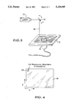
- FIG. 3 is a perspective view of a portion of the present invention.
- FIG. 4 is a plan view of a specimen to be scanned by the present inventive technique.
- the invention consists of an improved method utilizing five major hardware components as shown in FIG. 1, which is a block diagram of the present inventive system for laser induced eddy current imaging.
- the five major components are: a laser source 10, a pancake shape eddy current detecting coil 16, a lock-in amplifier 4, a system controller 2, and an impedance gain/phase analyzer 6.
- Other sub-components are modulator 8, scanning mirror 12 and specimen 14.
- Laser 10 is the excitation source and can be an argon-ion laser or another suitable laser.
- Laser 10 is modulated by modulator 8, which is essentially a cyclic function generator, producing a beam 18 which is directed by scanning mirror 12 to specimen 14.
- modulator 8 which is essentially a cyclic function generator, producing a beam 18 which is directed by scanning mirror 12 to specimen 14.
- a very localized or small area 20 of specimen 14 is impacted directly by beam 18, creating a thermal and stress wave 20 in specimen 14 and inducing thermal and elastic strains in specimen 14.
- Depth penetration by wave 20 is dependent upon the modulation frequency of modulator 8.
- An impedance gain/phase analyzer 6 such as is well known in the art, is connected to eddy current detecting coil 16. Analyzer 6 is in turn connected to lock-in amplifier 4 through system controller 2. The lock-in amplifier 4 is also synchronized to modulator 8. System controller 2 is used to control lock-in amplifier 4, scanning mirror 12, and to process data from analyzer 6. System controller can be an IBM series 386 PC or the equivalent.
- An example of a suitable impedance gain/phase analyzer 6 is an HP 4194A analyzer connected by an IEEE488 bus to controller 2.
- a typical eddy current detecting coil 16 is a Nortec surface probe SP-100. Lock-in amplifiers are well known in this art.
- FIG. 3 shows the raster scanning of beam 18 across specimen 14 which allows the detection by coil 16 of the laser generated thermal and elastic strains induced in specimen 14 by laser 10
- the rastering of beam 18 is controlled by controller 2 by positioning mirror 12. This technique is well known in the art.
- the method of detection of flaws in the present invention differs from that in the prior art as follows.
- signals from the lock-in amplifier resulted in a magnitude component and a phase component.
- Each of these components was sent to separate volt meters from the lock-in amp.
- the analog output signals of the volt meters was then summed with a signals from vertical and horizontal position sensors and fed into the vertical and horizontal channels of an x-y recorder.
- These signals at the x-y recorder presented the modulation of the impedance of the eddy-current probe and was synchronized with the chopped laser beam.
- the signal also represented an image of the sample at the location of the probe.
- the present inventive technique uses the absolute resistance and inductance of detector coil 16 vs. the arbitrary proportional signals of the prior art.
- the impedance of detector coil 16 can be expressed as: ##EQU1## where I is the current in detector coil 16, E and H are the electric and magnetic fields induced by coil 16, and s is the area enclosed by the electromagnetic field.
- the resistance R, where R Re(Z) is the real component of the impedance Z and the reactance X L where X L Im(Z) is the imaginary component.
- R and X L can be measured by a precision LCR impedance meter.
- the impedance change due to laser induced thermal strain and elastic strain in specimen 14 can be expressed as: ##EQU2## where ⁇ / ⁇ T is the electric conductivity ( ⁇ ) change and ⁇ / ⁇ T is the magnetic permeability ( ⁇ ) change of the material due to induced thermoelastic effect T.
- the coil 16 impedance change ⁇ Z, due to laser induced thermoelastic effects to the material is measured to be approximately 3 ⁇ or 20% for resistance and 4 ⁇ or 6% for reactance. Coordinating the impedance change with respect to specimen position, will allow advanced characterization of thermoelastic and defect properties of the material.
Abstract
An improved NDE method utilizes a laser source with modulator and scanning mirror, a pancake shape eddy current detecting coil, a lock-in amplifier, a system controller, and an impedance gain/phase analyzer. The laser is directed by the scanning mirror to a specimen to be analyzed. A very localized or small area of the specimen is impacted directly by the laser beam creating a thermal and stress wave in the specimen. An impedance gain/phase analyzer is connected to the eddy current detecting coil and to a lock-in amplifier through the system controller. The lock-in amplifier is also synchronized to the laser modulator. The system controller is used to control the lock-in amplifier, scanning mirror, and to process data from the analyzer. Raster scanning of the laser beam across the speciment allows the detection by the coil of the laser generated thermal and elastic strains induced in the specimen by the laser. The rastering of the laser beam is controlled by the controller by positioning the mirror.
Description
The invention described herein was made by an employee of the United States Government, and may be manufactured and used by or for the Government for governmental purposes without the payment of any royalties thereon or therefor.
This invention relates to Nondestructive Evaluation and in particular to a system utilizing an eddy current imaging system for the detection of laser generated thermal and elastic strains in materials for advanced material characterization.
Nondestructive Evaluation (NDE) uses tests to examine an object or material to detect imperfections, determine properties, or asses quality without changing its usefulness. NDE methods have been developed over the years using high powered optical techniques, ultrasonic surface wave measurement, stress fluorescent, penetrant techniques, and eddy current inspection analysis. This invention is primarily concerned with utilizing an eddy current imaging system for the detection of laser generated thermal and elastic strains in materials for advanced material characterization. This advanced technology can be used for surface displacement evaluation, defect detection and damage assessment.
Eddy-current probes have been used in the past as a form of NDE and recently in conjunction with photoinductive imaging. Photoinductive imaging is a unique dual-mode NDE technique that combines eddy current and thermal wave methods. The photoinductive effect, upon which this method is based, is the thermally induced change in the impedance of an eddy current probe in proximity to a conducting surface that is illuminated with a modulated light source. The change in probe impedance is caused by the temperature-induced changes in the conductivity and permeability of the specimen. Typical changes in probe impedance are small, on the order of a few ppm, but because they are synchronous with the light-beam modulation, lock-in techniques can be used to detect the signals, which can then be used to image surface or near-surface defects, voids, inclusions, or other thermal or structural inhomogeneities. The problems with the prior art photoinductive NDE has been that they offer only one side excitation and detection on the specimen and can only be used to examine very thin surface features within sub-microns.
It is therefore an object of the present invention to provide an improved method and apparatus for the detection of thermal strains in sample materials.
Another object of the invention is to provide an improved Nondestructive Evaluation technique.
A still further object of the invention is to provide an improved method for advanced materials characterization.
The foregoing objects and others are achieved by providing an improved NDE method utilizing five major hardware components: a laser source with modulator and scanning mirror, a pancake shape eddy current detecting coil, a lock-in amplifier, a system controller, and an impedance gain/phase analyzer. The laser is directed by the scanning mirror to a specimen to be analyzed. A very localized or small area of the specimen is impacted directly by the laser beam creating a thermal and stress wave in the specimen. Depth penetration by the thermal wave is dependent on the modulation frequency of the laser modulator.
An impedance gain/phase analyzer is connected to the eddy current detecting coil and to a lock-in amplifier through the system controller. The lock-in amplifier is also synchronized to the laser modulator. The system controller is used to control the lock-in amplifier, scanning mirror, and to process data from the analyzer. Raster scanning of the laser beam across the specimen allows the detection by the coil of the laser generated thermal and elastic strains induced in the specimen by the laser. The rastering of the laser beam is controlled by the controller by positioning the mirror.
The method of detection of flaws in the present invention differs from that in the prior art. The present inventive technique uses the absolute resistance and inductance of the detector coil vs. the arbitrary proportional signals of the prior art.
FIG. 1 is a block diagram of the components of the present invention.
FIG. 2 is a pictorial representation of the operation of the present invention.
FIG. 3 is a perspective view of a portion of the present invention.
FIG. 4 is a plan view of a specimen to be scanned by the present inventive technique.
The invention consists of an improved method utilizing five major hardware components as shown in FIG. 1, which is a block diagram of the present inventive system for laser induced eddy current imaging. The five major components are: a laser source 10, a pancake shape eddy current detecting coil 16, a lock-in amplifier 4, a system controller 2, and an impedance gain/phase analyzer 6. Other sub-components are modulator 8, scanning mirror 12 and specimen 14.
An impedance gain/phase analyzer 6, such as is well known in the art, is connected to eddy current detecting coil 16. Analyzer 6 is in turn connected to lock-in amplifier 4 through system controller 2. The lock-in amplifier 4 is also synchronized to modulator 8. System controller 2 is used to control lock-in amplifier 4, scanning mirror 12, and to process data from analyzer 6. System controller can be an IBM series 386 PC or the equivalent. An example of a suitable impedance gain/phase analyzer 6 is an HP 4194A analyzer connected by an IEEE488 bus to controller 2. A typical eddy current detecting coil 16 is a Nortec surface probe SP-100. Lock-in amplifiers are well known in this art.
FIG. 3 shows the raster scanning of beam 18 across specimen 14 which allows the detection by coil 16 of the laser generated thermal and elastic strains induced in specimen 14 by laser 10 The rastering of beam 18 is controlled by controller 2 by positioning mirror 12. This technique is well known in the art.
The method of detection of flaws in the present invention differs from that in the prior art as follows. In the prior art, signals from the lock-in amplifier resulted in a magnitude component and a phase component. Each of these components was sent to separate volt meters from the lock-in amp. The analog output signals of the volt meters was then summed with a signals from vertical and horizontal position sensors and fed into the vertical and horizontal channels of an x-y recorder. These signals at the x-y recorder presented the modulation of the impedance of the eddy-current probe and was synchronized with the chopped laser beam. The signal also represented an image of the sample at the location of the probe. The present inventive technique uses the absolute resistance and inductance of detector coil 16 vs. the arbitrary proportional signals of the prior art.
From fundamental theories of electromagnetism, the impedance of detector coil 16 can be expressed as: ##EQU1## where I is the current in detector coil 16, E and H are the electric and magnetic fields induced by coil 16, and s is the area enclosed by the electromagnetic field. Coil 16 impedance Z is normally expressed as a complex quantity, Z=R+jXL. The resistance R, where R Re(Z) is the real component of the impedance Z and the reactance XL where XL =Im(Z) is the imaginary component. R and XL can be measured by a precision LCR impedance meter.
The impedance change due to laser induced thermal strain and elastic strain in specimen 14 can be expressed as: ##EQU2## where ζσ/ζT is the electric conductivity (σ) change and ζμ/ζT is the magnetic permeability (μ) change of the material due to induced thermoelastic effect T.
For example, the coil 16 impedance Z of a 100 kHz pancake probe at ambient temperature is experimentally measured to be: Resistance R=14.3Ω and Reactance XL =82.5Ω. The coil 16 impedance change ΔZ, due to laser induced thermoelastic effects to the material is measured to be approximately 3Ω or 20% for resistance and 4Ω or 6% for reactance. Coordinating the impedance change with respect to specimen position, will allow advanced characterization of thermoelastic and defect properties of the material.
To those skilled in the art, many modifications and variations of the present invention are possible in light of the above teachings. It is therefore to be understood that the present invention can be practiced otherwise than as specifically described herein and still will be within the spirit and scope of the appended claims.
Claims (4)
1. An apparatus for advanced characterization of a material specimen comprising:
a laser;
a modulator modulating said laser;
a scanning mirror for directing a beam from said laser on said material specimen thereby inducing thermal and elastic strains in said specimen;
an eddy current detecting coil adjacent said specimen for detecting changes in electrical conductivity in said specimen caused by said thermal and elastic strains in said specimen;
an impedance gain/phase analyzer, for measuring said the absolute resistance and inductance of said coil as a result of said changes in electrical conductivity in said specimen, connected to said detecting coil;
a lock-in amplifier connected to said modulator; and
a system controller for data acquisition and control connected to said impedance gain/phase analyzer, said lock-in amplifier and said scanning mirror.
2. The apparatus of claim 1 wherein said scanning mirror directs said beam on said specimen in a raster fashion.
3. A method for advanced characterization of a material specimen comprising the steps of:
positioning said specimen adjacent an eddy current detecting coil;
generating a modulated thermal source;
directing said modulated thermal source onto said specimen at a localized area on said specimen;
scanning said localized area across said specimen to cause generation of thermal and stress wave in said specimen;
detecting with said coil changes in electrical conductivity and magnetic permeability in the localized areas caused by localized thermal and stress changes in said specimen; and
measuring the absolute resistance and inductance of said coil so as to thereby directly characterize said material specimen.
4. The method of claim 3 wherein said scanning is done in a raster fashion across said specimen.
Priority Applications (4)
| Application Number | Priority Date | Filing Date | Title |
|---|---|---|---|
| US07/758,977 US5124640A (en) | 1991-09-05 | 1991-09-05 | Method for advanced material characterization by laser induced eddy current imaging |
| EP19920307989 EP0531127A3 (en) | 1991-09-05 | 1992-09-03 | Method for advanced material characterization by laser induced eddy current imaging |
| CA002077462A CA2077462A1 (en) | 1991-09-05 | 1992-09-03 | Method for advanced material characterization by laser induced eddy current imaging |
| JP4238670A JPH05256824A (en) | 1991-09-05 | 1992-09-07 | Method and apparatus for displaying characteristics of material improved by image formation of eddy current induced by laser |
Applications Claiming Priority (1)
| Application Number | Priority Date | Filing Date | Title |
|---|---|---|---|
| US07/758,977 US5124640A (en) | 1991-09-05 | 1991-09-05 | Method for advanced material characterization by laser induced eddy current imaging |
Publications (1)
| Publication Number | Publication Date |
|---|---|
| US5124640A true US5124640A (en) | 1992-06-23 |
Family
ID=25053890
Family Applications (1)
| Application Number | Title | Priority Date | Filing Date |
|---|---|---|---|
| US07/758,977 Expired - Fee Related US5124640A (en) | 1991-09-05 | 1991-09-05 | Method for advanced material characterization by laser induced eddy current imaging |
Country Status (4)
| Country | Link |
|---|---|
| US (1) | US5124640A (en) |
| EP (1) | EP0531127A3 (en) |
| JP (1) | JPH05256824A (en) |
| CA (1) | CA2077462A1 (en) |
Cited By (13)
| Publication number | Priority date | Publication date | Assignee | Title |
|---|---|---|---|---|
| EP0531127A2 (en) * | 1991-09-05 | 1993-03-10 | National Aeronautics And Space Administration | Method for advanced material characterization by laser induced eddy current imaging |
| US5463201A (en) * | 1993-02-04 | 1995-10-31 | Generla Electric Company | Seam-tracking apparatus for a welding system employing an array of eddy current elements |
| US7139083B2 (en) * | 2000-09-20 | 2006-11-21 | Kla-Tencor Technologies Corp. | Methods and systems for determining a composition and a thickness of a specimen |
| US20070230536A1 (en) * | 2006-03-28 | 2007-10-04 | Mtu Aero Engines Gmbh | Method and apparatus for detection of flaws in a metal component |
| US20080067455A1 (en) * | 2006-06-15 | 2008-03-20 | Siemens Power Generation, Inc. | Hand held magnetic induction thermography system |
| US7349090B2 (en) | 2000-09-20 | 2008-03-25 | Kla-Tencor Technologies Corp. | Methods and systems for determining a property of a specimen prior to, during, or subsequent to lithography |
| US20090000382A1 (en) * | 2006-07-31 | 2009-01-01 | University Of Dayton | Non-contact acousto-thermal method and apparatus for detecting incipient damage in materials |
| US7716987B2 (en) | 2006-07-31 | 2010-05-18 | University Of Dayton | Non-contact thermo-elastic property measurement and imaging system for quantitative nondestructive evaluation of materials |
| US7751046B2 (en) | 2000-09-20 | 2010-07-06 | Kla-Tencor Technologies Corp. | Methods and systems for determining a critical dimension and overlay of a specimen |
| US20100292938A1 (en) * | 2009-05-15 | 2010-11-18 | Vrana Johannes L | Automated Inspection System and Method for Nondestructive Inspection of a Workpiece Using Induction Thermography |
| US20110048135A1 (en) * | 2009-08-25 | 2011-03-03 | Caron James N | Continuous Laser Generation of Ultrasound |
| WO2013173698A1 (en) * | 2012-05-18 | 2013-11-21 | The Trustees Of Columbia University In The City Of New York | System, method and computer-accessible medium for providing fluorescence attenuation |
| CN104236769A (en) * | 2014-10-14 | 2014-12-24 | 西安炬光科技有限公司 | Method and device for testing residual stress distribution of semiconductor laser chips |
Families Citing this family (2)
| Publication number | Priority date | Publication date | Assignee | Title |
|---|---|---|---|---|
| FR2760529B1 (en) * | 1997-03-05 | 1999-05-28 | Framatome Sa | PROCESS FOR PHOTOTHERMAL EXAMINATION OF A PART |
| JP2007127590A (en) * | 2005-11-07 | 2007-05-24 | Nec Electronics Corp | Method and system for inspecting semiconductor device |
Citations (1)
| Publication number | Priority date | Publication date | Assignee | Title |
|---|---|---|---|---|
| US4950990A (en) * | 1989-07-21 | 1990-08-21 | Iowa State University Research Foundation, Inc. | Method and apparatus for photoinductive imaging |
Family Cites Families (2)
| Publication number | Priority date | Publication date | Assignee | Title |
|---|---|---|---|---|
| US5015950A (en) * | 1989-07-21 | 1991-05-14 | Iowa State University Research Foundation, Inc. | Method and apparatus for determining thermal resistance and structural integrity of coatings on conducting materials by monitoring electrical conductance of the underlying material upon localized heating of the overlying coating |
| US5124640A (en) * | 1991-09-05 | 1992-06-23 | The United States Of Americas As Represented By The Administrator Of The National Aeronautics & Space Administration | Method for advanced material characterization by laser induced eddy current imaging |
-
1991
- 1991-09-05 US US07/758,977 patent/US5124640A/en not_active Expired - Fee Related
-
1992
- 1992-09-03 EP EP19920307989 patent/EP0531127A3/en not_active Withdrawn
- 1992-09-03 CA CA002077462A patent/CA2077462A1/en not_active Abandoned
- 1992-09-07 JP JP4238670A patent/JPH05256824A/en not_active Withdrawn
Patent Citations (1)
| Publication number | Priority date | Publication date | Assignee | Title |
|---|---|---|---|---|
| US4950990A (en) * | 1989-07-21 | 1990-08-21 | Iowa State University Research Foundation, Inc. | Method and apparatus for photoinductive imaging |
Non-Patent Citations (6)
| Title |
|---|
| International Advances in Nondestructive Testing, 1989, pp. 175 218. * |
| International Advances in Nondestructive Testing, 1989, pp. 175-218. |
| McGraw Hill Encyclopedia of Science & Technology, vol. 11, 1987, pp. 28 33. * |
| McGraw-Hill Encyclopedia of Science & Technology, vol. 11, 1987, pp. 28-33. |
| Review of Progress in Quantititative Nondestructive Evaluation, vol. 9, 1990, pp. 533 538. * |
| Review of Progress in Quantititative Nondestructive Evaluation, vol. 9, 1990, pp. 533-538. |
Cited By (21)
| Publication number | Priority date | Publication date | Assignee | Title |
|---|---|---|---|---|
| EP0531127A3 (en) * | 1991-09-05 | 1993-12-01 | Nasa | Method for advanced material characterization by laser induced eddy current imaging |
| EP0531127A2 (en) * | 1991-09-05 | 1993-03-10 | National Aeronautics And Space Administration | Method for advanced material characterization by laser induced eddy current imaging |
| US5463201A (en) * | 1993-02-04 | 1995-10-31 | Generla Electric Company | Seam-tracking apparatus for a welding system employing an array of eddy current elements |
| US8179530B2 (en) | 2000-09-20 | 2012-05-15 | Kla-Tencor Technologies Corp. | Methods and systems for determining a critical dimension and overlay of a specimen |
| US7139083B2 (en) * | 2000-09-20 | 2006-11-21 | Kla-Tencor Technologies Corp. | Methods and systems for determining a composition and a thickness of a specimen |
| US7349090B2 (en) | 2000-09-20 | 2008-03-25 | Kla-Tencor Technologies Corp. | Methods and systems for determining a property of a specimen prior to, during, or subsequent to lithography |
| US7460981B2 (en) | 2000-09-20 | 2008-12-02 | Kla-Tencor Technologies Corp. | Methods and systems for determining a presence of macro and micro defects on a specimen |
| US8502979B2 (en) | 2000-09-20 | 2013-08-06 | Kla-Tencor Technologies Corp. | Methods and systems for determining a critical dimension and overlay of a specimen |
| US7751046B2 (en) | 2000-09-20 | 2010-07-06 | Kla-Tencor Technologies Corp. | Methods and systems for determining a critical dimension and overlay of a specimen |
| US20070230536A1 (en) * | 2006-03-28 | 2007-10-04 | Mtu Aero Engines Gmbh | Method and apparatus for detection of flaws in a metal component |
| US20080067455A1 (en) * | 2006-06-15 | 2008-03-20 | Siemens Power Generation, Inc. | Hand held magnetic induction thermography system |
| US7485882B2 (en) | 2006-06-15 | 2009-02-03 | Siemens Energy, Inc. | Hand held magnetic induction thermography system |
| US7716987B2 (en) | 2006-07-31 | 2010-05-18 | University Of Dayton | Non-contact thermo-elastic property measurement and imaging system for quantitative nondestructive evaluation of materials |
| US20090000382A1 (en) * | 2006-07-31 | 2009-01-01 | University Of Dayton | Non-contact acousto-thermal method and apparatus for detecting incipient damage in materials |
| US20100292938A1 (en) * | 2009-05-15 | 2010-11-18 | Vrana Johannes L | Automated Inspection System and Method for Nondestructive Inspection of a Workpiece Using Induction Thermography |
| US8527215B2 (en) | 2009-05-15 | 2013-09-03 | Siemens Energy, Inc. | Automated inspection system and method for nondestructive inspection of a workpiece using induction thermography |
| US20110048135A1 (en) * | 2009-08-25 | 2011-03-03 | Caron James N | Continuous Laser Generation of Ultrasound |
| US8210045B2 (en) * | 2009-08-25 | 2012-07-03 | James N. Caron | Continuous laser generation of ultrasound |
| WO2013173698A1 (en) * | 2012-05-18 | 2013-11-21 | The Trustees Of Columbia University In The City Of New York | System, method and computer-accessible medium for providing fluorescence attenuation |
| CN104236769A (en) * | 2014-10-14 | 2014-12-24 | 西安炬光科技有限公司 | Method and device for testing residual stress distribution of semiconductor laser chips |
| CN104236769B (en) * | 2014-10-14 | 2017-04-12 | 西安炬光科技股份有限公司 | Method and device for testing residual stress distribution of semiconductor laser chips |
Also Published As
| Publication number | Publication date |
|---|---|
| EP0531127A3 (en) | 1993-12-01 |
| JPH05256824A (en) | 1993-10-08 |
| CA2077462A1 (en) | 1993-03-06 |
| EP0531127A2 (en) | 1993-03-10 |
Similar Documents
| Publication | Publication Date | Title |
|---|---|---|
| US4755753A (en) | Eddy current surface mapping system for flaw detection | |
| US5124640A (en) | Method for advanced material characterization by laser induced eddy current imaging | |
| US4950990A (en) | Method and apparatus for photoinductive imaging | |
| US4207519A (en) | Method and apparatus for detecting defects in workpieces using a core-type magnet with magneto-sensitive detectors | |
| JPS60152950A (en) | Eddy current nondestructive testing method and device thereof | |
| CN112378930A (en) | Pulse laser-based cladding layer surface and deep layer flaw detection method | |
| JP3753499B2 (en) | Magnetic flaw detection apparatus and method | |
| Finkel et al. | Electromagnetically induced acoustic emission—novel NDT technique for damage evaluation | |
| Moulder et al. | Characterizing the performance of eddy current probes using photoinductive field-mapping | |
| Cheng et al. | Application of the magneto-optic Faraday effect in NDT | |
| Moulder et al. | Photoinductive imaging: a new NDE technique | |
| US5019775A (en) | Calibrating an eddy-current-probe using a modulated thermal energy source | |
| EP0479918A1 (en) | Method and apparatus for photoinductive imaging | |
| Pasadas et al. | Eddy current testing of cracks using multi-frequency and noise excitation | |
| Smetana et al. | Austenitic Biomaterial Cracks Evaluation by Advanced Nondestructive Techniques | |
| JP2000131287A (en) | Method and device for detecting flaw using magnetic measurement | |
| Lee et al. | Application of magneto-optical method for inspection of the internal surface of a tube | |
| Sullivan et al. | Comparing a one-dimensional skin effect equation with through transmission eddy current phenomena: British journal of non-destructive testing, Vol. 32, No. 2, pp. 71–75 (Feb. 1990) | |
| Chichigin et al. | Study and quantitative assessment of the structural inhomogeneities parameters of composite materials | |
| Vertiy et al. | eddy Current tomography Applications | |
| JP2519501Y2 (en) | Magnetic flaw detector | |
| Chady et al. | Eddy current testing of concrete structures | |
| Moulder et al. | Calibration and characterization of eddy current probes by photoinductive field mapping | |
| Postolache et al. | Uniform eddy current probe implementation using planar excitation coil and GMR sensor array | |
| Rummel et al. | Assessment of the Effects of Scanning Variations and Eddy Current Probe Type on Crack Detection |
Legal Events
| Date | Code | Title | Description |
|---|---|---|---|
| AS | Assignment |
Owner name: UNITED STATES OF AMERICA, THE, AS REPRESENTED BY T Free format text: ASSIGNMENT OF ASSIGNORS INTEREST.;ASSIGNOR:CHERN, ENGMIN J.;REEL/FRAME:005846/0329 Effective date: 19910830 |
|
| REMI | Maintenance fee reminder mailed | ||
| LAPS | Lapse for failure to pay maintenance fees | ||
| FP | Lapsed due to failure to pay maintenance fee |
Effective date: 19960626 |
|
| STCH | Information on status: patent discontinuation |
Free format text: PATENT EXPIRED DUE TO NONPAYMENT OF MAINTENANCE FEES UNDER 37 CFR 1.362 |