US5128560A - Boosted supply output driver circuit for driving an all N-channel output stage - Google Patents
Boosted supply output driver circuit for driving an all N-channel output stage Download PDFInfo
- Publication number
- US5128560A US5128560A US07/673,746 US67374691A US5128560A US 5128560 A US5128560 A US 5128560A US 67374691 A US67374691 A US 67374691A US 5128560 A US5128560 A US 5128560A
- Authority
- US
- United States
- Prior art keywords
- output
- input
- coupled
- channel
- logic
- Prior art date
- Legal status (The legal status is an assumption and is not a legal conclusion. Google has not performed a legal analysis and makes no representation as to the accuracy of the status listed.)
- Expired - Lifetime
Links
Images


Classifications
-
- H—ELECTRICITY
- H02—GENERATION; CONVERSION OR DISTRIBUTION OF ELECTRIC POWER
- H02M—APPARATUS FOR CONVERSION BETWEEN AC AND AC, BETWEEN AC AND DC, OR BETWEEN DC AND DC, AND FOR USE WITH MAINS OR SIMILAR POWER SUPPLY SYSTEMS; CONVERSION OF DC OR AC INPUT POWER INTO SURGE OUTPUT POWER; CONTROL OR REGULATION THEREOF
- H02M7/00—Conversion of ac power input into dc power output; Conversion of dc power input into ac power output
- H02M7/42—Conversion of dc power input into ac power output without possibility of reversal
- H02M7/44—Conversion of dc power input into ac power output without possibility of reversal by static converters
- H02M7/48—Conversion of dc power input into ac power output without possibility of reversal by static converters using discharge tubes with control electrode or semiconductor devices with control electrode
- H02M7/53—Conversion of dc power input into ac power output without possibility of reversal by static converters using discharge tubes with control electrode or semiconductor devices with control electrode using devices of a triode or transistor type requiring continuous application of a control signal
- H02M7/537—Conversion of dc power input into ac power output without possibility of reversal by static converters using discharge tubes with control electrode or semiconductor devices with control electrode using devices of a triode or transistor type requiring continuous application of a control signal using semiconductor devices only, e.g. single switched pulse inverters
- H02M7/538—Conversion of dc power input into ac power output without possibility of reversal by static converters using discharge tubes with control electrode or semiconductor devices with control electrode using devices of a triode or transistor type requiring continuous application of a control signal using semiconductor devices only, e.g. single switched pulse inverters in a push-pull configuration
-
- H—ELECTRICITY
- H03—ELECTRONIC CIRCUITRY
- H03K—PULSE TECHNIQUE
- H03K19/00—Logic circuits, i.e. having at least two inputs acting on one output; Inverting circuits
- H03K19/0175—Coupling arrangements; Interface arrangements
- H03K19/0185—Coupling arrangements; Interface arrangements using field effect transistors only
- H03K19/018507—Interface arrangements
Definitions
- This invention relates generally to output driver circuits for driving the inputs of an output stage, and more particularly to those output driver circuits capable of driving the inputs of an all N-channel output stage with a boosted voltage.
- FIGS. 1A and 1B Two types of field-effect transistor (“FET”) output stages are shown in FIGS. 1A and 1B.
- output stage 20 has two N-channel transistors 22 and 24.
- Transistor 22 is normally referred to as a "pullup” transistor, and transistor 24 is normally referred to as a “pulldown” transistor.
- the gates of transistors 22 and 24 form first and second inputs 23 and 25.
- the drain of transistor 22 is coupled to a supply voltage VCC, typically five volts, at terminal 21.
- the source of transistor 24 is coupled to a negative supply voltage or ground at terminal 28.
- the source of transistor 22 and the drain of transistor 24 are coupled together to form an output 32.
- the first and second inputs 23 and 25 are complementary and are therefore driven differentially.
- input 23 is coupled to a logic low voltage and input 25 is coupled to a logic high voltage.
- transistor 22 is biased off and transistor 24 is biased on, effectively shorting output 32 to ground through the low drain-to-source resistance of transistor 24 and isolating output 32 from the supply voltage through the high drain-to-source resistance of transistor 24.
- the polarities of the signals at inputs 23 and 25 are inverted.
- inputs 23 and 25 can also both be held low to turn off both transistors 22 and 24.
- output stage 20A has a P-channel pullup transistor 22A and an N-channel pulldown transistor 24.
- the gates of transistors 22 and 24 form first and second inputs 23 and 25.
- the source of transistor 22 is coupled to the supply voltage VCC at terminal 21 and the source of transistor 24 is coupled to ground at terminal 28.
- the drains of transistors 22 and 24 are coupled together to form the output 32.
- inputs 23 and 25 In a normal mode of operation, the first and second inputs 23 and 25 require the same polarity to switch the output 32. Therefore, inputs 23 and 25 can be coupled together to the same logic input signal. However, if a tristate output feature is desired, inputs 23 and 25 can be driven with two logic input signals.
- To produce a logic low voltage at output 32 inputs 23 and 25 are coupled together and to a logic high voltage. Thus, transistor 22A is biased off and transistor 24 is biased on, effectively shorting output 32 to ground and isolating output 32 from the supply voltage in the manner described above.
- a logic low voltage is coupled to inputs 23 and 25, which biases on transistor 22A and biases off transistor 24.
- output stage 20 is generally preferred. Since output stage 20 uses no P-channel transistors, the possibility of latch-up is minimized. However, in operation, the logic high voltage at the output 32 is diminished by the gate-to-source voltage required to bias on transistor 22. For example, if the input 23 is driven by a five volt signal, the VCC supply voltage is five volts, and the threshold voltage of transistor 22 is about one volt, then the output voltage at output 32 is about four volts. The output voltage can be even less of a load is coupled to output 32. The gate-to-source voltage drop of transistor 22 is usually not a problem since the minimum allowable logic high threshold of subsequent stages is less than four volts.
- TTL logic levels are 2.4 volts for a minimum logic high threshold and 0.8 volts for a maximum logic low threshold. Therefore, as long as the power supply voltage VCC is kept at five volts, output stage 20 is capable of driving most TTL standard loads.
- gate widths of transistors used in a 4 megabit random access memory (“RAM”) can be 0.6 ⁇ m to 0.8 ⁇ m or even less, while gate oxide can be 150 Angstroms to 200 Angstroms or less.
- the intensity of the electric field generated by a five volt power supply can affect the reliability of or even destroy and integrated circuit fabricated with sub-micron feature size transistors. Consequently, a lower power supply voltage such as 3.3 volts must be used to preserve the reliability and functionality of sub-micron integrated circuits.
- output stage 20 can no longer be used.
- the voltage at the output 32 can be 2.3 volts unloaded or 2.0 volts loaded. This output voltage is not sufficient to drive a subsequent stage.
- the output voltage provided is within the "forbidden zone" between the allowable logic high and logic low TTL threshold levels and is therefore not a valid logic signal.
- a prior method of providing a valid output voltage at the output 32 of the N-channel output stage 20 increased the voltage drive only at input 23.
- An output driver circuit was used to increase the voltage input above the level of the lower voltage power supply.
- output driver circuits for increasing the voltage at input 23 typically involved complex circuitry having critical timing or delay paths.
- an object of the present invention to implement an output driver circuit with a simple design using a minimum number of transistors and having no critical timing or delay paths.
- an output driver circuit includes first and second translator circuits and a boosted voltage generator.
- the output driver circuit is suitable for driving the first and second inputs of a reduced voltage N-channel output stage.
- the first and second translator circuits each have a power terminal and an input for receiving first and second logic input signals.
- a boost voltage generator having a boosted voltage output is respectively coupled to the power terminals of the first and second translator circuits.
- the first translator circuit has an output coupled to the first input of the N-channel output stage for providing a boosted logic output signal in a logic high polarity state.
- the second translator circuit has an output coupled to the second input of the N-channel output stage for providing a boosted logic output signal in a logic high polarity state.
- the outputs of the first and second translator circuits are complementary for driving the N-channel output stage to provide a valid output logic signal.
- the outputs of the first and second translator circuits are both low for placing the N-channel output stage into a high impedance tristate mode.
- FIGS. 1A-1B are schematic diagrams of two types of output stages.
- FIG. 2 is a combined block/schematic diagram of a an output driver circuit according to the present invention interposed between a logic block and an N-channel output stage.
- FIGS. 3-4 are schematic diagrams of translator circuits suitable for use in the output driver circuit of FIG. 2.
- FIG. 5 is a schematic diagram of an inverter suitable for use in the translator circuits of FIGS. 3-4.
- FIG. 6 is a plot of the typical voltage characteristics versus time of the output of the translator circuit of FIG. 3.
- FIG. 7 is a combined block/schematic diagram of a boosted voltage generator suitable for use with the output driver circuit of FIG. 2.
- FIG. 8 is a more detailed block/schematic diagram of the boosted voltage generator of FIG. 6.
- FIG. 9 is a detailed schematic diagram of the ring oscillator depicted in FIG. 8.
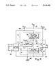
- an output driver circuit 10 suitable for driving an N-channel output stage 20 includes a first translator circuit 14, a second translator circuit 16, and a boosted voltage generator 18.
- Logic input signals 13 and 15 are provided to the input of output driver circuit 10 by logic block 12.
- Logic block 12 represents any combination of logic circuitry having one or more input terminals 30 designated IN 1 through IN 2 . Therefore, logic input signals 13 and 15 represent any desired logic signals, which may or may not be complementary. The nature of the logic input signals 13 and 15 depends only upon the output characteristics desired, as is explained in greater detail below.
- the N-channel output stage 20 has first and second inputs 23 and 25 that are driven by the outputs of translator circuits 14 and 16.
- Power for the output driver circuit 10, the logic block 12, and the N-channel output stage 20 is provided by a positive power supply voltage V CC at terminal 21 and ground or a negative power supply voltage at terminal 28.
- the power supply voltage differential between terminals 21 and 28 is typically a reduced voltage of 3.3 volts suitable for high-density, sub-micron integrated circuits.
- separate power supplies VCC1 and VCC2 may be used.
- a first power supply, VCC1 at terminal 26, is used to provide power for the logic block 12 and the boosted voltage generator 18, whereas a second power supply, VCC2 at terminal 27, is used to provide power for the N-channel output stage 20.
- Separate power supplies enable different voltages to be used in order to further adjust output characteristics.
- the first and second translator circuits 14 and 16 translate the low logic levels of the logic block 12 into complementary boosted logic levels that drive the inputs 23 and 25 of the N-channel output stage 20. If V CC is equal to a reduced voltage of 3.3 volts, the logic levels of the logic block 12 output are 3.3 volts for a logic high and zero volts for a logic low. Assuming that a translator circuit 14 or 16 is non-inverting, a logic high of 3.3 volts presented to the input produces a logic high at the output of 5 volts. A logic low of zero volts presented to the input produces a logic low at the output of zero volts.
- a logic high of 3.3 volts presented to the input produces a logic low at the output of zero volts.
- a logic low of zero volts presented to the input produces a logic high at the output of 5 volts.
- the logic block 12 and the first and second translator circuits 14 and 16 cooperate to place the output stage 20 into one of two modes.
- output stage 20 provides a valid logic signal, either high or low.
- output stage 20 provides a high impedance tristate mode. Therefore, the polarity of the logic block 12 and the translator circuits 14 and 16 is selected to provide the proper logic levels to the output stage 20.
- the necessary inversion to drive the output stage 20 in the first mode can be provided either by adjusting the polarity of the input logic signals 13 and 15, or the polarity of translator circuits 14 and 16.
- the first translator circuit 14 has a power terminal, an input for receiving the first logic input signal, and an output coupled to the first input 23 of the N-channel output stage for providing a boosted logic output signal in a logic high polarity state.
- the second translator circuit 16 has a power terminal, an input for receiving the second logic input signal, and an output coupled to the second input 25 of the N-channel output stage for providing a boosted logic output signal in a logic high polarity state.
- the outputs of the first and second translator circuits 14 and 16 are complementary for properly driving the output stage 20 and are both low for placing the output stage 20 into a tristate mode.
- the boost voltage generator 18 has a boosted voltage output 34 respectively coupled to the power terminals of the first and second translator circuits 14 and 16.
- a noninverting translator circuit 40 suitable for use as the first or second translator circuit 14 or 16 is shown in FIG. 3 and includes an N-channel pass transistor 42, a P-channel transistor 44, and an inverter 46.
- the pass transistor 42 has a gate 21 coupled to the positive supply voltage, V CC , a first controlled node (drain or source since field-effect transistors are symmetrical) forming the input 41 of the translator circuit, and a second controlled node forming the output 43 of the translator circuit 40.
- the P-channel transistor 44 has a first controlled node forming the power terminal of the translator circuit coupled to the boosted voltage, V CCP , at terminal 34.
- the second controlled node of the P-channel transistor 44 is coupled to the output of the translator circuit 43.
- the inverter 46 has an input coupled to the output 43 of the translator circuit, an output coupled to the gate of the P-channel transistor 44.
- the positive power terminal of the inverter 46 is coupled to the power terminal of the translator circuit 40 at terminal 34.
- the translator circuit 40 of FIG. 3 converts a reduced voltage logic high of about 3.3 volts to a boosted voltage logic high of about 5 volts.
- the N-channel pass transistor 42 applies the input voltage to the output terminal 43.
- the reduced voltage logic high is coupled to the input of the inverter 46 and is sufficient to change logic states of the inverter.
- the inverter 46 provides a logic low to the gate of the P-channel transistor 44, which causes transistor 44 to conduct. Since the source of the P-channel transistor 44 is coupled to the boosted voltage supply, V CCP , the drain, which is output terminal 43, is pulled high. Therefore, a short time after a logic high is presented to the input terminal 41, a boosted logic high appears at the output terminal 43.
- Terminal 43 initially switches to 2.3 volts because of the voltage drop across the pass transistor 42, then switches to 5 volts once the inverter 46 changes logic states. Total switching time takes between 1 and 3 nanoseconds, depending upon the semiconductor process and transistor size. If a logic low is presented at input terminal 41, the inverter 46 provides a logic low to the gate of the P-channel transistor 44, which causes transistor 44 to turn off. Since the P-channel transistor 44 is off, the drain presents a high impedance to the output terminal 43, which remains low.
- An inverting translator circuit 50 suitable for use as the first or second translator circuits 14 or 16 is shown in FIG. 4 and includes an N-channel pass transistor 52, A P-channel transistor 54, and an inverter 56.
- the pass transistor 52 has a gate coupled to the positive supply voltage, V CC , a first controlled node forming the input 51 of the translator circuit, and a second controlled node.
- the P-channel transistor 54 has a gate forming the output 53 of the translator circuit 50.
- a first controlled node forms the power terminal of the translator circuit coupled to the boosted voltage, V CCP , at terminal 34.
- a second controlled node of the P-channel transistor 54 is coupled to the second controlled node of the pass transistor 52.
- the inverter 56 has an input coupled to the second controlled node of the pass transistor 52 and an output coupled to the output 53 of the translator circuit.
- the positive power terminal of the inverter 56 is coupled to the power terminal of the translator circuit 50 at terminal 34.
- the inverting translator circuit 50 of FIG. 4 converts a logic zero to a boosted voltage logic one of about 5 volts.
- the N-channel pass transistor 52 applies the input voltage of zero volts to the input of the inverter 56.
- the output of inverter 56 provides a logic high to the gate of the P-channel channel transistor 54, which causes transistor 54 to turn off. Since the P-channel transistor 54 is off, the drain presents a high impedance to the output terminal 53, which remains low. In the case of a reduced voltage logic high of about 2.3 volts, the logic high is coupled to the input of the inverter 56 and is sufficient to change logic states of the inverter.
- the inverter 56 provides a logic low to the gate of the P-channel transistor 54, which causes transistor 54 to conduct. Since the source of the P-channel transistor 54 is coupled to the boosted voltage supply, V CCP , the drain, which is coupled to the input of the inverter 56 is pulled high, thus ensuring a logic zero at terminal 53.
- the P-channel transistor 54 is desirably included to prevent any possibility of DC current flow through inverter 56.
- An inverter 60 is shown in FIG. 5 that is suitable for use as the inverters 46 and 56 in the translator circuits 14 and 16.
- the source of a first P-channel transistor 62 forms the power terminal of the inverter coupled to the boosted power supply voltage, V CCP .
- a second actively-biased P-channel transistor 63 has a source coupled to the drain of the first P-channel transistor 62.
- a first N-channel transistor 64 has a source coupled to ground.
- a second actively-biased N-channel transistor 65 has a source coupled to the drain of the first N-channel transistor 64.
- the gates of the first P-channel transistor 62 and the first N-channel transistor 64 are coupled together to form the input 66 of inverter 60.
- the drains of the second P-channel transistor 63 and the second N-channel transistor 65 are coupled together to form the output 68 of inverter 60.
- Transistors 63 and 65 are included to reduce the total voltage and consequently, electric field, across each of the four transistors.
- a boost voltage generator 18 is shown in greater detail in FIG. 7 and includes a level shifting circuit 70 having an input coupled to the boosted voltage and a voltage shifted output 72.
- a load element 80 is coupled between the output 72 of the level shifting circuit and ground.
- An inverter 90, 92 has input coupled to the output 72 of the level shifting circuit and an output formed at the coupled drains of a P-channel transistor 90 and an N-channel transistor 92. If desired, an hysteresis stage 100 can be included in the output of the inverter to provide a sharp control signal with no bouncing.
- a charge pump 110 has an input coupled to the output of the inverter 90, 92 or the hysteresis stage 100 and an output coupled to the boosted voltage output, V CCP , at node 34.
- the boosted voltage is maintained by the action of the charge pump 110, which is periodically turned on if the boosted voltage drops below a predetermined value.
- a sense circuit including the level shifting circuit 70 and the load element 80 provides a control voltage to turn on the charge pump 110.
- the charge pump pumps charge into the boosted voltage terminal 34 until the boosted voltage V CCP , returns to the nominal value.
- the sense circuit then provides a control voltage to turn off the charge pump 110.
- the level shifting circuit 70 can include one or more serially-connected diodes or diode connected transistors.
- the load element 80 can be a polysilicon resistor, a well of a first polarity type integrated in a semiconductor substrate of a second polarity type, or the drain-to-source resistance of a transistor.
- the boosted voltage generator 18 is shown in greater detail in FIG. 8.
- the level shifting circuit 70 includes two diode connected N-channel transistors 74 and 76 and a diode connected P-channel transistor 72.
- the P-channel transistor 72 is a level shifting element that provides a better match in threshold voltage shift with P-channel transistor 90 over process variations.
- the load element 80 is shown as the drain to source resistance of an actively biased N-channel transistor 80.
- the hysteresis function is provided by an inverter including transistors 104 and 105 having a feedback circuit including transistors 102, 103, and 106. A variable resistive path is presented to ground to create the hysteresis.
- transistor 102 is biased off and the resistance coupled to the P-channel transistor 90 is provided by N-channel transistor 92. In another mode, transistor 102 is biased on and the resistance coupled to the P-channel transistor 90 is equal to the parallel combination of transistors 92 and 102.
- the charge pump 110 includes an even number of serially-connected inverter stages such as inverters 111 and 112, the input of the first inverter forming the input of the charge pump 110. Inverters 111 and 112 are used to buffer the drive signal from the inverter 90, 92.
- a ring oscillator 113 has an input 122 coupled to the output of a last inverter stage and an output 124 for providing an oscillating digital signal. As shown in greater detail in FIG.
- the ring oscillator 113 typical includes an odd number of inverters such as NAND gate 126 and serially-connected inverter stages 128.
- the ring oscillator 113 can also incorporate inverters 111 and 112.
- the input of a first inverter stage or NAND gate 126 forms the input 122 of the ring oscillator 113 and the output 124 of a last inverter stage forms the output 124 of the ring oscillator 113.
- the output of the last inverter stage is also coupled directly or through NAND gate 126 to the input of the first inverter stage to create the oscillation.
- a capacitor 114 is coupled to the output of the ring oscillator 113.
- a first diode 115 has an anode coupled to the low voltage supply voltage VCC and a cathode coupled to the capacitor 114.
- a second diode 116 has an anode coupled to the capacitor and a cathode forming the output of the charge pump 110.
- the digital oscillating signal of the ring oscillator 113 in conjunction with the capacitor 114 and diodes 115 and 116, provide a means for delivering charge in one direction to terminal 34.
- the oscillating signal is at a logic low, the junction of the two diodes 115 and 116 is at about 3 volts, the charge on capacitor 114 also being about 3 volts.
- the oscillating signal switches to a logic high, the junction between the two diodes is boosted to over five volts.
- diode 115 is off and diode 116 is on, delivering charge to the boosted voltage terminal.
- an output driver circuit is implemented with a simple design using a minimum number of circuit elements.
- the translator circuits used in the output driver circuit have no critical timing or delay paths.
- the configuration of the output driver circuit has two independent voltage outputs for increasing the voltage drive at the gates of both of the output transistors.
- the higher gate voltage provided by the output driver circuit for both the pullup and pulldown output transistors establishes a valid output logic level having both a higher logic high level and a lower logic low level. Since the drive to the gates of the output drivers is provided by the output driver circuit, the output voltage of the output stage is substantially isolated from the noise and fluctuations of the external power supply. Also because of the higher drive voltages, smaller output devices with lower capacitance can be used.
Abstract
An output driver circuit includes first and second translator circuits and a boosted voltage generator. The output driver circuit is suitable for driving the first and second inputs of a reduced voltage N-channel output stage. The first and second translator circuits each have a power terminal and an input for receiving first and second logic input signals. A boost voltage generator having a boosted voltage output is respectively coupled to the power terminals of the first and second translator circuits. The first translator circuit has an output coupled to the first input of the N-channel output stage for providing a boosted logic output signal in a logic high polarity state. The second translator circuit has an output coupled to the second input of the N-channel output stage for providing a boosted logic output signal in a logic high polarity state. The outputs of the first and second translator circuits are complementary for driving the N-channel output stage to provide a valid output logic signal. Alternatively, the outputs of the first and second translator circuits are both low for placing the N-channel output stage into a high impedance tristate mode.
Description
This invention relates generally to output driver circuits for driving the inputs of an output stage, and more particularly to those output driver circuits capable of driving the inputs of an all N-channel output stage with a boosted voltage.
Two types of field-effect transistor ("FET") output stages are shown in FIGS. 1A and 1B. Referring to FIG. 1A, output stage 20 has two N- channel transistors 22 and 24. Transistor 22 is normally referred to as a "pullup" transistor, and transistor 24 is normally referred to as a "pulldown" transistor. The gates of transistors 22 and 24 form first and second inputs 23 and 25. The drain of transistor 22 is coupled to a supply voltage VCC, typically five volts, at terminal 21. The source of transistor 24 is coupled to a negative supply voltage or ground at terminal 28. The source of transistor 22 and the drain of transistor 24 are coupled together to form an output 32.
In a normal mode of operation, the first and second inputs 23 and 25 are complementary and are therefore driven differentially. To produce a logic low voltage at output 32, input 23 is coupled to a logic low voltage and input 25 is coupled to a logic high voltage. Thus, transistor 22 is biased off and transistor 24 is biased on, effectively shorting output 32 to ground through the low drain-to-source resistance of transistor 24 and isolating output 32 from the supply voltage through the high drain-to-source resistance of transistor 24. To produce a logic high voltage at output 32, the polarities of the signals at inputs 23 and 25 are inverted. In a high impedance or "tristate" output mode, inputs 23 and 25 can also both be held low to turn off both transistors 22 and 24.
Referring to FIG. 1B, output stage 20A has a P-channel pullup transistor 22A and an N-channel pulldown transistor 24. As output state 20, the gates of transistors 22 and 24 form first and second inputs 23 and 25. The source of transistor 22 is coupled to the supply voltage VCC at terminal 21 and the source of transistor 24 is coupled to ground at terminal 28. The drains of transistors 22 and 24 are coupled together to form the output 32.
In a normal mode of operation, the first and second inputs 23 and 25 require the same polarity to switch the output 32. Therefore, inputs 23 and 25 can be coupled together to the same logic input signal. However, if a tristate output feature is desired, inputs 23 and 25 can be driven with two logic input signals. To produce a logic low voltage at output 32, inputs 23 and 25 are coupled together and to a logic high voltage. Thus, transistor 22A is biased off and transistor 24 is biased on, effectively shorting output 32 to ground and isolating output 32 from the supply voltage in the manner described above. To produce a logic high voltage at output 32, a logic low voltage is coupled to inputs 23 and 25, which biases on transistor 22A and biases off transistor 24.
Of the two output stages 20 and 20A shown in FIGS. 1A and 1B, output stage 20 is generally preferred. Since output stage 20 uses no P-channel transistors, the possibility of latch-up is minimized. However, in operation, the logic high voltage at the output 32 is diminished by the gate-to-source voltage required to bias on transistor 22. For example, if the input 23 is driven by a five volt signal, the VCC supply voltage is five volts, and the threshold voltage of transistor 22 is about one volt, then the output voltage at output 32 is about four volts. The output voltage can be even less of a load is coupled to output 32. The gate-to-source voltage drop of transistor 22 is usually not a problem since the minimum allowable logic high threshold of subsequent stages is less than four volts. For example, typical valid TTL logic levels are 2.4 volts for a minimum logic high threshold and 0.8 volts for a maximum logic low threshold. Therefore, as long as the power supply voltage VCC is kept at five volts, output stage 20 is capable of driving most TTL standard loads.
However, as the feature sizes of transistors shrink to enable higher levels of integration on a single integrated circuit, five volts can no longer be used as the power supply voltage. For example, gate widths of transistors used in a 4 megabit random access memory ("RAM") can be 0.6 μm to 0.8 μm or even less, while gate oxide can be 150 Angstroms to 200 Angstroms or less. The intensity of the electric field generated by a five volt power supply can affect the reliability of or even destroy and integrated circuit fabricated with sub-micron feature size transistors. Consequently, a lower power supply voltage such as 3.3 volts must be used to preserve the reliability and functionality of sub-micron integrated circuits.
While a lower voltage power supply solves the problem of intense electric fields, output stage 20 can no longer be used. With a 3.3 volt power supply, the voltage at the output 32 can be 2.3 volts unloaded or 2.0 volts loaded. This output voltage is not sufficient to drive a subsequent stage. The output voltage provided is within the "forbidden zone" between the allowable logic high and logic low TTL threshold levels and is therefore not a valid logic signal.
A prior method of providing a valid output voltage at the output 32 of the N-channel output stage 20 increased the voltage drive only at input 23. An output driver circuit was used to increase the voltage input above the level of the lower voltage power supply. However, such output driver circuits for increasing the voltage at input 23 typically involved complex circuitry having critical timing or delay paths.
Therefore, what is desired is a simple output driver circuit without any critical timing or delay paths for increasing the output voltage of an N-channel output stage coupled to a reduced voltage power supply.
It is, therefore, an object of the present invention to implement an output driver circuit with a simple design using a minimum number of transistors and having no critical timing or delay paths.
It is another object of the present invention to implement an output driver circuit having two voltage outputs for increasing the voltage drive at the gates of both of the output transistors.
It is an advantage of the present invention in that the higher gate voltage provided by the output driver circuit for both the pullup and pulldown output transistors establishes a valid output logic level having a higher logic high level and a lower logic low level.
It is another advantage of the present invention that the output voltage of the output stage is substantially isolated from noise and fluctuations of the external power supply.
It is a further advantage of the present invention that, because of the higher drive voltages, smaller output devices with lower capacitance can be used.
It is still a further advantage of the present invention that elevated voltage drive levels are well controlled, substantially isolating the output voltage from changes in the external VCC supply voltage.
According to the present invention, an output driver circuit includes first and second translator circuits and a boosted voltage generator. The output driver circuit is suitable for driving the first and second inputs of a reduced voltage N-channel output stage. The first and second translator circuits each have a power terminal and an input for receiving first and second logic input signals. A boost voltage generator having a boosted voltage output is respectively coupled to the power terminals of the first and second translator circuits. The first translator circuit has an output coupled to the first input of the N-channel output stage for providing a boosted logic output signal in a logic high polarity state. The second translator circuit has an output coupled to the second input of the N-channel output stage for providing a boosted logic output signal in a logic high polarity state. The outputs of the first and second translator circuits are complementary for driving the N-channel output stage to provide a valid output logic signal. Alternatively, the outputs of the first and second translator circuits are both low for placing the N-channel output stage into a high impedance tristate mode.
The foregoing and other objects, features and advantages of the invention will become more readily apparent from the following detailed description of a preferred embodiment which proceeds with reference to the drawings.
FIGS. 1A-1B are schematic diagrams of two types of output stages.
FIG. 2 is a combined block/schematic diagram of a an output driver circuit according to the present invention interposed between a logic block and an N-channel output stage.
FIGS. 3-4 are schematic diagrams of translator circuits suitable for use in the output driver circuit of FIG. 2.
FIG. 5 is a schematic diagram of an inverter suitable for use in the translator circuits of FIGS. 3-4.
FIG. 6 is a plot of the typical voltage characteristics versus time of the output of the translator circuit of FIG. 3.
FIG. 7 is a combined block/schematic diagram of a boosted voltage generator suitable for use with the output driver circuit of FIG. 2.
FIG. 8 is a more detailed block/schematic diagram of the boosted voltage generator of FIG. 6.
FIG. 9 is a detailed schematic diagram of the ring oscillator depicted in FIG. 8.
Referring to FIG. 2, an output driver circuit 10 suitable for driving an N-channel output stage 20 includes a first translator circuit 14, a second translator circuit 16, and a boosted voltage generator 18. Logic input signals 13 and 15 are provided to the input of output driver circuit 10 by logic block 12. Logic block 12 represents any combination of logic circuitry having one or more input terminals 30 designated IN1 through IN2. Therefore, logic input signals 13 and 15 represent any desired logic signals, which may or may not be complementary. The nature of the logic input signals 13 and 15 depends only upon the output characteristics desired, as is explained in greater detail below. The N-channel output stage 20 has first and second inputs 23 and 25 that are driven by the outputs of translator circuits 14 and 16.
Power for the output driver circuit 10, the logic block 12, and the N-channel output stage 20 is provided by a positive power supply voltage VCC at terminal 21 and ground or a negative power supply voltage at terminal 28. The power supply voltage differential between terminals 21 and 28 is typically a reduced voltage of 3.3 volts suitable for high-density, sub-micron integrated circuits. Alternatively, separate power supplies VCC1 and VCC2, may be used. A first power supply, VCC1 at terminal 26, is used to provide power for the logic block 12 and the boosted voltage generator 18, whereas a second power supply, VCC2 at terminal 27, is used to provide power for the N-channel output stage 20. Separate power supplies enable different voltages to be used in order to further adjust output characteristics.
In operation, the first and second translator circuits 14 and 16 translate the low logic levels of the logic block 12 into complementary boosted logic levels that drive the inputs 23 and 25 of the N-channel output stage 20. If VCC is equal to a reduced voltage of 3.3 volts, the logic levels of the logic block 12 output are 3.3 volts for a logic high and zero volts for a logic low. Assuming that a translator circuit 14 or 16 is non-inverting, a logic high of 3.3 volts presented to the input produces a logic high at the output of 5 volts. A logic low of zero volts presented to the input produces a logic low at the output of zero volts. Assuming that a translator circuit 14 or 16 is inverting, a logic high of 3.3 volts presented to the input produces a logic low at the output of zero volts. A logic low of zero volts presented to the input produces a logic high at the output of 5 volts.
The logic block 12 and the first and second translator circuits 14 and 16 cooperate to place the output stage 20 into one of two modes. In a first mode, output stage 20 provides a valid logic signal, either high or low. In a second mode, output stage 20 provides a high impedance tristate mode. Therefore, the polarity of the logic block 12 and the translator circuits 14 and 16 is selected to provide the proper logic levels to the output stage 20. The necessary inversion to drive the output stage 20 in the first mode can be provided either by adjusting the polarity of the input logic signals 13 and 15, or the polarity of translator circuits 14 and 16.
The first translator circuit 14 has a power terminal, an input for receiving the first logic input signal, and an output coupled to the first input 23 of the N-channel output stage for providing a boosted logic output signal in a logic high polarity state. The second translator circuit 16 has a power terminal, an input for receiving the second logic input signal, and an output coupled to the second input 25 of the N-channel output stage for providing a boosted logic output signal in a logic high polarity state. As previously explained, the outputs of the first and second translator circuits 14 and 16 are complementary for properly driving the output stage 20 and are both low for placing the output stage 20 into a tristate mode. The boost voltage generator 18 has a boosted voltage output 34 respectively coupled to the power terminals of the first and second translator circuits 14 and 16.
A noninverting translator circuit 40 suitable for use as the first or second translator circuit 14 or 16 is shown in FIG. 3 and includes an N-channel pass transistor 42, a P-channel transistor 44, and an inverter 46. The pass transistor 42 has a gate 21 coupled to the positive supply voltage, VCC, a first controlled node (drain or source since field-effect transistors are symmetrical) forming the input 41 of the translator circuit, and a second controlled node forming the output 43 of the translator circuit 40. The P-channel transistor 44 has a first controlled node forming the power terminal of the translator circuit coupled to the boosted voltage, VCCP, at terminal 34. The second controlled node of the P-channel transistor 44 is coupled to the output of the translator circuit 43. The inverter 46 has an input coupled to the output 43 of the translator circuit, an output coupled to the gate of the P-channel transistor 44. The positive power terminal of the inverter 46 is coupled to the power terminal of the translator circuit 40 at terminal 34.
In operation, the translator circuit 40 of FIG. 3 converts a reduced voltage logic high of about 3.3 volts to a boosted voltage logic high of about 5 volts. The N-channel pass transistor 42 applies the input voltage to the output terminal 43. The reduced voltage logic high is coupled to the input of the inverter 46 and is sufficient to change logic states of the inverter. The inverter 46 provides a logic low to the gate of the P-channel transistor 44, which causes transistor 44 to conduct. Since the source of the P-channel transistor 44 is coupled to the boosted voltage supply, VCCP, the drain, which is output terminal 43, is pulled high. Therefore, a short time after a logic high is presented to the input terminal 41, a boosted logic high appears at the output terminal 43. This is best seen in the plot of voltage versus time of terminal 43 in FIG. 6. Terminal 43 initially switches to 2.3 volts because of the voltage drop across the pass transistor 42, then switches to 5 volts once the inverter 46 changes logic states. Total switching time takes between 1 and 3 nanoseconds, depending upon the semiconductor process and transistor size. If a logic low is presented at input terminal 41, the inverter 46 provides a logic low to the gate of the P-channel transistor 44, which causes transistor 44 to turn off. Since the P-channel transistor 44 is off, the drain presents a high impedance to the output terminal 43, which remains low.
An inverting translator circuit 50 suitable for use as the first or second translator circuits 14 or 16 is shown in FIG. 4 and includes an N-channel pass transistor 52, A P-channel transistor 54, and an inverter 56. The pass transistor 52 has a gate coupled to the positive supply voltage, VCC, a first controlled node forming the input 51 of the translator circuit, and a second controlled node. The P-channel transistor 54 has a gate forming the output 53 of the translator circuit 50. A first controlled node forms the power terminal of the translator circuit coupled to the boosted voltage, VCCP, at terminal 34. A second controlled node of the P-channel transistor 54 is coupled to the second controlled node of the pass transistor 52. The inverter 56 has an input coupled to the second controlled node of the pass transistor 52 and an output coupled to the output 53 of the translator circuit. The positive power terminal of the inverter 56 is coupled to the power terminal of the translator circuit 50 at terminal 34.
In operation, the inverting translator circuit 50 of FIG. 4 converts a logic zero to a boosted voltage logic one of about 5 volts. The N-channel pass transistor 52 applies the input voltage of zero volts to the input of the inverter 56. The output of inverter 56 provides a logic high to the gate of the P-channel channel transistor 54, which causes transistor 54 to turn off. Since the P-channel transistor 54 is off, the drain presents a high impedance to the output terminal 53, which remains low. In the case of a reduced voltage logic high of about 2.3 volts, the logic high is coupled to the input of the inverter 56 and is sufficient to change logic states of the inverter. The inverter 56 provides a logic low to the gate of the P-channel transistor 54, which causes transistor 54 to conduct. Since the source of the P-channel transistor 54 is coupled to the boosted voltage supply, VCCP, the drain, which is coupled to the input of the inverter 56 is pulled high, thus ensuring a logic zero at terminal 53. The P-channel transistor 54 is desirably included to prevent any possibility of DC current flow through inverter 56.
An inverter 60 is shown in FIG. 5 that is suitable for use as the inverters 46 and 56 in the translator circuits 14 and 16. The source of a first P-channel transistor 62 forms the power terminal of the inverter coupled to the boosted power supply voltage, VCCP. A second actively-biased P-channel transistor 63 has a source coupled to the drain of the first P-channel transistor 62. A first N-channel transistor 64 has a source coupled to ground. A second actively-biased N-channel transistor 65 has a source coupled to the drain of the first N-channel transistor 64. The gates of the first P-channel transistor 62 and the first N-channel transistor 64 are coupled together to form the input 66 of inverter 60. The drains of the second P-channel transistor 63 and the second N-channel transistor 65 are coupled together to form the output 68 of inverter 60. Transistors 63 and 65 are included to reduce the total voltage and consequently, electric field, across each of the four transistors.
A boost voltage generator 18 is shown in greater detail in FIG. 7 and includes a level shifting circuit 70 having an input coupled to the boosted voltage and a voltage shifted output 72. A load element 80 is coupled between the output 72 of the level shifting circuit and ground. An inverter 90, 92 has input coupled to the output 72 of the level shifting circuit and an output formed at the coupled drains of a P-channel transistor 90 and an N-channel transistor 92. If desired, an hysteresis stage 100 can be included in the output of the inverter to provide a sharp control signal with no bouncing. A charge pump 110 has an input coupled to the output of the inverter 90, 92 or the hysteresis stage 100 and an output coupled to the boosted voltage output, VCCP, at node 34.
In operation, the boosted voltage is maintained by the action of the charge pump 110, which is periodically turned on if the boosted voltage drops below a predetermined value. When the boosted value changes from a nominal value, a sense circuit including the level shifting circuit 70 and the load element 80 provides a control voltage to turn on the charge pump 110. In turn, the charge pump pumps charge into the boosted voltage terminal 34 until the boosted voltage VCCP, returns to the nominal value. The sense circuit then provides a control voltage to turn off the charge pump 110.
If desired, the level shifting circuit 70 can include one or more serially-connected diodes or diode connected transistors. The load element 80 can be a polysilicon resistor, a well of a first polarity type integrated in a semiconductor substrate of a second polarity type, or the drain-to-source resistance of a transistor.
The boosted voltage generator 18 is shown in greater detail in FIG. 8. The level shifting circuit 70 includes two diode connected N- channel transistors 74 and 76 and a diode connected P-channel transistor 72. The P-channel transistor 72 is a level shifting element that provides a better match in threshold voltage shift with P-channel transistor 90 over process variations. The load element 80 is shown as the drain to source resistance of an actively biased N-channel transistor 80. The hysteresis function is provided by an inverter including transistors 104 and 105 having a feedback circuit including transistors 102, 103, and 106. A variable resistive path is presented to ground to create the hysteresis. In one mode, transistor 102 is biased off and the resistance coupled to the P-channel transistor 90 is provided by N-channel transistor 92. In another mode, transistor 102 is biased on and the resistance coupled to the P-channel transistor 90 is equal to the parallel combination of transistors 92 and 102. The charge pump 110 includes an even number of serially-connected inverter stages such as inverters 111 and 112, the input of the first inverter forming the input of the charge pump 110. Inverters 111 and 112 are used to buffer the drive signal from the inverter 90, 92. A ring oscillator 113 has an input 122 coupled to the output of a last inverter stage and an output 124 for providing an oscillating digital signal. As shown in greater detail in FIG. 9, the ring oscillator 113 typical includes an odd number of inverters such as NAND gate 126 and serially-connected inverter stages 128. The ring oscillator 113 can also incorporate inverters 111 and 112. The input of a first inverter stage or NAND gate 126 forms the input 122 of the ring oscillator 113 and the output 124 of a last inverter stage forms the output 124 of the ring oscillator 113. The output of the last inverter stage is also coupled directly or through NAND gate 126 to the input of the first inverter stage to create the oscillation. Referring back to FIG. 8, a capacitor 114 is coupled to the output of the ring oscillator 113. A first diode 115 has an anode coupled to the low voltage supply voltage VCC and a cathode coupled to the capacitor 114. A second diode 116 has an anode coupled to the capacitor and a cathode forming the output of the charge pump 110.
In operation, the digital oscillating signal of the ring oscillator 113 in conjunction with the capacitor 114 and diodes 115 and 116, provide a means for delivering charge in one direction to terminal 34. When the oscillating signal is at a logic low, the junction of the two diodes 115 and 116 is at about 3 volts, the charge on capacitor 114 also being about 3 volts. When the oscillating signal switches to a logic high, the junction between the two diodes is boosted to over five volts. Thus, diode 115 is off and diode 116 is on, delivering charge to the boosted voltage terminal.
It has been demonstrated that an output driver circuit is implemented with a simple design using a minimum number of circuit elements. The translator circuits used in the output driver circuit have no critical timing or delay paths. The configuration of the output driver circuit has two independent voltage outputs for increasing the voltage drive at the gates of both of the output transistors. The higher gate voltage provided by the output driver circuit for both the pullup and pulldown output transistors establishes a valid output logic level having both a higher logic high level and a lower logic low level. Since the drive to the gates of the output drivers is provided by the output driver circuit, the output voltage of the output stage is substantially isolated from the noise and fluctuations of the external power supply. Also because of the higher drive voltages, smaller output devices with lower capacitance can be used.
Having illustrated and described the principles of my invention in a preferred embodiment, it should be readily apparent to those skilled in the art that the invention can be modified in arrangement and detail without departing from such principles. For example, the exact circuitry of the first and second translator circuits 14 and 15 can be modified without departing from the scope of the invention. Therefore, we claim all modifications coming within the true spirit and scope of the accompanying claims.
Claims (22)
1. An output circuit comprising:
an N-channel output stage having first and second inputs and a power terminal coupled to a non-boosted voltage supply:
a first translator circuit having a power terminal, an input for receiving a first logic input signal, and an output coupled to the first input of the N-channel output stage for providing a boosted logic output signal in a logic high polarity state;
a second translator circuit having a power terminal, an input for receiving a second logic input signal, and an output coupled to the second input of the N-channel output stage for providing a boosted logic output signal in a logic high polarity state; and
a boost voltage generator having a boosted voltage output respectively coupled to the power terminals of the first and second translator circuits.
2. An output circuit as in claim 1 in which at least one of the first and second translator circuits comprise:
means for coupling one of the first and second logic signals to the output; and
single inverter means for sensing a logic high level at the output and thereafter providing a boosted logic high level to the output.
3. An output circuit as in claim 2 in which the coupling means comprises a pass transistor having a control node coupled to a source of constant supply voltage, a first controlled node forming the input of the translator circuit, and a second controlled node forming the output of the translator circuit.
4. An output circuit as in claim 2 in which the single inverter means comprises:
a P-channel transistor having a control node, a first controlled node forming the power terminal of the translator circuit, and a second controlled node coupled to the output of the translator circuit; and
an inverter having an input coupled to the output of the translator circuit, an output coupled to the control node of the P-channel transistor, and a power terminal coupled to the power terminal of the translator circuit.
5. An output circuit as in claim 4 in which the inverter comprises:
a first P-channel transistor having a gate, a drain, and a source forming the power terminal of the inverter;
a second actively-biased P-channel transistor having a drain and a source coupled to the drain of the first P-channel transistor;
a first N-channel transistor having a gate, a drain, and a source coupled to ground;
a second actively-biased N-channel transistor having a drain and a source coupled to the drain of the first N-channel transistor, wherein the gates of the first P-channel and the first N-channel transistors are coupled together to form the input, and the drains of the second P-channel and the second N-channel transistors are coupled together to form the output.
6. An output circuit as in claim 1 in which at least one of the first and second translator circuits comprise:
means for coupling one of the first and second logic signals to an intermediate node; and
single inverter means for sensing a logic high level at the intermediate node and thereafter providing a boosted logic high level to the output.
7. An output circuit as in claim 6 in which the coupling means comprises a pass transistor having a control node coupled to a source of constant supply voltage, a first controlled node forming the input of the translator circuit, and a second controlled node coupled to the intermediate node.
8. An output circuit as in claim 6 in which the single inverter means comprises:
a P-channel transistor having a control node forming the output of the translator circuit, a first controlled node forming the power terminal of the translator circuit, and a second controlled node coupled to the intermediate node; and
an inverter having an input coupled to the intermediate node, an output forming the output of the translator circuit, and a power terminal coupled to the power terminal of the translator circuit.
9. An output circuit as in claim 8 in which the inverter comprises:
a first P-channel transistor having a gate, a drain, and a source forming the power terminal of the inverter;
a second actively-biased P-channel transistor having a drain and a source coupled to the drain of the first P-channel transistor;
a first N-channel transistor having a gate, a drain, and a source coupled to ground;
a second actively-biased N-channel transistor having a drain and a source coupled to the drain of the first N-channel transistor,
wherein the gates of the first P-channel and the first N-channel transistors are coupled together to form the input, and the drains of the second P-channel nd the second N-channel transistors are coupled together to form the output.
10. An output circuit as in claim 1 in which the boost voltage generator comprises:
a level shifting circuit having first and second nodes, the first node being coupled to the boosted voltage output;
a load element coupled between the second node of the level shifting circuit and ground;
an inverter having an input, an output, and the input being coupled to the second node of the level shifting circuit;
a charge pump having an input coupled to the output of the inverter and an output coupled to the boosted voltage output; and
a capacitor coupled between the boosted voltage output and ground.
11. An output circuit as in claim 10 in which the level shifting circuit comprises one or more serially-connected diodes.
12. An output circuit as in claim 10 in which the load element comprises a polysilicon resistor.
13. An output circuit as in claim 10 in which the load element comprises a well of a first polarity type integrated in a semiconductor substrate of a second polarity type.
14. An output circuit as in claim 10 in which the load element comprises the drain-to-source resistance of a transistor.
15. An output circuit as in claim 10 in which the inverter comprises a hysteresis switching-threshold inverter.
16. An output circuit as in claim 10 in which the charge pump comprises:
an even plurality of serially-connected inverter stages, each inverter stage having an input and an output, the input of a first inverter stage forming the input of the charge pump;
a ring oscillator having an input and an output, the input being coupled to the output of a last inverter stage;
a capacitor having a first node and a second node, the first node being coupled to the output of the ring oscillator;
a first diode having an anode coupled to a source of constant supply voltage and a cathode coupled to the second node of the capacitor; and
a second diode having an anode coupled to the second node of the capacitor and a cathode forming the output of the charge pump.
17. An output circuit as in claim 16 in which the ring oscillator comprises an odd plurality of serially-connected inverter stages, each inverter having an input and an output, the input of a first inverter stage forming the input of the ring oscillator, the output of a last inverter stage forming the output of the ring oscillator, and the output of the last inverter stage being coupled to the input of the first inverter stage.
18. A method for driving an N-channel output stage having first and second inputs and a power terminal, the method comprising:
generating a first and second input logic signals;
translating the first input logic signal into a first boosted logic signal, wherein the first boosted logic signal has a logic high level greater than a logic high level of the first input logic signal;
translating the second input logic signal into a second boosted logic signal, wherein the second boosted logic signal has a logic high level greater than a logic high level of the second input logic signal;
driving the first input of the N-channel output stage with the first boosted logic signal;
driving the second input of the N-channel output stage with the second boosted logic signal; and
coupling the power terminal of the N-channel output stage to a non-boosted voltage supply.
19. A method for driving an N-channel output stage as in claim 18 in which the step of translating the first input logic signal comprises:
coupling the first logic signals to the first input of the N-channel output stage;
sensing a logic high level at the first input of the N-channel output stage; and
providing a boosted logic high level to the first input of the N-channel output stage.
20. A method for driving an N-channel output stage as in claim 18 in which the step of translating the second input logic signal comprises:
coupling the second logic signals to the second input of the N-channel output stage;
sensing a logic high level at the second input of the N-channel output stage; and
providing a boosted logic high level to the second input of the N-channel output stage.
21. A method for driving an N-channel output stage as in claim 18 in which the step of translating the first input logic signal comprises:
coupling the first logic signal to an intermediate node;
sensing a logic high level at the intermediate node; and
providing a boosted logic high level to the first input of the N-channel output stage.
22. A method for driving an N-channel output stage as in claim 18 in which the step of translating the second input logic signal comprises:
coupling the second logic signal to an intermediate node;
sensing a logic high level at the intermediate node; and
providing a boosted logic high level to the second input of the N-channel output stage.
Priority Applications (1)
| Application Number | Priority Date | Filing Date | Title |
|---|---|---|---|
| US07/673,746 US5128560A (en) | 1991-03-22 | 1991-03-22 | Boosted supply output driver circuit for driving an all N-channel output stage |
Applications Claiming Priority (1)
| Application Number | Priority Date | Filing Date | Title |
|---|---|---|---|
| US07/673,746 US5128560A (en) | 1991-03-22 | 1991-03-22 | Boosted supply output driver circuit for driving an all N-channel output stage |
Publications (1)
| Publication Number | Publication Date |
|---|---|
| US5128560A true US5128560A (en) | 1992-07-07 |
Family
ID=24703970
Family Applications (1)
| Application Number | Title | Priority Date | Filing Date |
|---|---|---|---|
| US07/673,746 Expired - Lifetime US5128560A (en) | 1991-03-22 | 1991-03-22 | Boosted supply output driver circuit for driving an all N-channel output stage |
Country Status (1)
| Country | Link |
|---|---|
| US (1) | US5128560A (en) |
Cited By (119)
| Publication number | Priority date | Publication date | Assignee | Title |
|---|---|---|---|---|
| US5204557A (en) * | 1991-10-15 | 1993-04-20 | National Semiconductor Corporation | Digital signal level translator |
| US5300835A (en) * | 1993-02-10 | 1994-04-05 | Cirrus Logic, Inc. | CMOS low power mixed voltage bidirectional I/O buffer |
| US5300832A (en) * | 1992-11-10 | 1994-04-05 | Sun Microsystems, Inc. | Voltage interfacing buffer with isolation transistors used for overvoltage protection |
| US5399920A (en) * | 1993-11-09 | 1995-03-21 | Texas Instruments Incorporated | CMOS driver which uses a higher voltage to compensate for threshold loss of the pull-up NFET |
| US5406140A (en) * | 1993-06-07 | 1995-04-11 | National Semiconductor Corporation | Voltage translation and overvoltage protection |
| WO1995019660A1 (en) * | 1994-01-13 | 1995-07-20 | Atmel Corporation | Breakdown protection circuit using high voltage detection |
| US5504450A (en) * | 1993-12-08 | 1996-04-02 | At&T Corp. | High voltage components for EEPROM system |
| US5532621A (en) * | 1993-12-24 | 1996-07-02 | Kawasaki Steel Corporation | Output buffer circuit, input buffer circuit and bi-directional buffer circuit for plural voltage systems |
| US5578941A (en) * | 1995-08-23 | 1996-11-26 | Micron Technology, Inc. | Voltage compensating CMOS input buffer circuit |
| US5614859A (en) * | 1995-08-04 | 1997-03-25 | Micron Technology, Inc. | Two stage voltage level translator |
| US5627487A (en) * | 1995-06-28 | 1997-05-06 | Micron Technology, Inc. | Charge conserving driver circuit for capacitive loads |
| US5644265A (en) * | 1995-05-01 | 1997-07-01 | International Business Machines Corporation | Off-chip driver for mixed voltage applications |
| US5666045A (en) * | 1994-12-09 | 1997-09-09 | Psc Inc. | Laser drive and control systems useful for laser diode protection |
| US5719506A (en) * | 1995-09-26 | 1998-02-17 | Xilinx, Inc. | Fast signal path for programmable logic device |
| WO1998011667A1 (en) * | 1996-09-12 | 1998-03-19 | Quality Semiconductor, Inc. | Mixed mode cmos input buffer with bus hold |
| US5736887A (en) * | 1996-01-25 | 1998-04-07 | Rockwell International Corporation | Five volt tolerant protection circuit |
| US5742197A (en) * | 1993-11-18 | 1998-04-21 | Samsung Electronics Co., Ltd. | Boosting voltage level detector for a semiconductor memory device |
| EP0847624A1 (en) * | 1996-06-25 | 1998-06-17 | Actel Corporation | Multiple logic family compatible output driver |
| US5783948A (en) * | 1995-06-23 | 1998-07-21 | Micron Technology, Inc. | Method and apparatus for enhanced booting and DC conditions |
| US5786711A (en) * | 1995-06-17 | 1998-07-28 | Samsung Electronics, Co., Ltd. | Data output buffer for use in a semiconductor memory device |
| US5801569A (en) * | 1995-10-31 | 1998-09-01 | Hyundai Electronics America | Output driver for mixed supply voltage systems |
| US5802009A (en) * | 1997-04-28 | 1998-09-01 | Micron Technology, Inc. | Voltage compensating output driver circuit |
| US5838177A (en) * | 1997-01-06 | 1998-11-17 | Micron Technology, Inc. | Adjustable output driver circuit having parallel pull-up and pull-down elements |
| US5869984A (en) * | 1994-01-13 | 1999-02-09 | Fujitsu Limited | Output buffer circuit utilizing FETS for lowering output resistance of a circuit block |
| US5870347A (en) * | 1997-03-11 | 1999-02-09 | Micron Technology, Inc. | Multi-bank memory input/output line selection |
| US5872736A (en) * | 1996-10-28 | 1999-02-16 | Micron Technology, Inc. | High speed input buffer |
| US5898638A (en) * | 1997-03-11 | 1999-04-27 | Micron Technology, Inc. | Latching wordline driver for multi-bank memory |
| US5900750A (en) * | 1997-08-15 | 1999-05-04 | Lsi Logic Corporation | 5V output driver on 2.5V technology |
| US5917758A (en) * | 1996-11-04 | 1999-06-29 | Micron Technology, Inc. | Adjustable output driver circuit |
| US5920518A (en) * | 1997-02-11 | 1999-07-06 | Micron Technology, Inc. | Synchronous clock generator including delay-locked loop |
| US5923594A (en) * | 1998-02-17 | 1999-07-13 | Micron Technology, Inc. | Method and apparatus for coupling data from a memory device using a single ended read data path |
| US5926047A (en) * | 1997-08-29 | 1999-07-20 | Micron Technology, Inc. | Synchronous clock generator including a delay-locked loop signal loss detector |
| US5926034A (en) * | 1997-08-14 | 1999-07-20 | Micron Technology, Inc. | Fuse option for multiple logic families on the same die |
| US5929656A (en) * | 1997-05-16 | 1999-07-27 | Motorola, Inc. | Method and apparatus for driving a capacitive display device |
| US5933386A (en) * | 1997-12-23 | 1999-08-03 | Mitsubishi Semiconductor America, Inc. | Driving memory bitlines using boosted voltage |
| US5940608A (en) * | 1997-02-11 | 1999-08-17 | Micron Technology, Inc. | Method and apparatus for generating an internal clock signal that is synchronized to an external clock signal |
| US5946244A (en) * | 1997-03-05 | 1999-08-31 | Micron Technology, Inc. | Delay-locked loop with binary-coupled capacitor |
| US5949254A (en) * | 1996-11-26 | 1999-09-07 | Micron Technology, Inc. | Adjustable output driver circuit |
| US5953284A (en) * | 1997-07-09 | 1999-09-14 | Micron Technology, Inc. | Method and apparatus for adaptively adjusting the timing of a clock signal used to latch digital signals, and memory device using same |
| EP0942535A1 (en) * | 1998-03-09 | 1999-09-15 | Siemens Aktiengesellschaft | Tri-state buffers |
| US5956502A (en) * | 1997-03-05 | 1999-09-21 | Micron Technology, Inc. | Method and circuit for producing high-speed counts |
| US6011732A (en) * | 1997-08-20 | 2000-01-04 | Micron Technology, Inc. | Synchronous clock generator including a compound delay-locked loop |
| US6014759A (en) * | 1997-06-13 | 2000-01-11 | Micron Technology, Inc. | Method and apparatus for transferring test data from a memory array |
| US6016282A (en) * | 1998-05-28 | 2000-01-18 | Micron Technology, Inc. | Clock vernier adjustment |
| US6025738A (en) * | 1997-08-22 | 2000-02-15 | International Business Machines Corporation | Gain enhanced split drive buffer |
| US6029250A (en) * | 1998-09-09 | 2000-02-22 | Micron Technology, Inc. | Method and apparatus for adaptively adjusting the timing offset between a clock signal and digital signals transmitted coincident with that clock signal, and memory device and system using same |
| US6034563A (en) * | 1995-10-19 | 2000-03-07 | Mitsubishi Denki Kabushiki Kaisha | Semiconductor integrated circuit having reduced current leakage and high speed |
| EP0703670B1 (en) * | 1994-09-26 | 2000-03-08 | Nec Corporation | Output buffer circuit |
| US6044429A (en) * | 1997-07-10 | 2000-03-28 | Micron Technology, Inc. | Method and apparatus for collision-free data transfers in a memory device with selectable data or address paths |
| US6057718A (en) * | 1997-02-26 | 2000-05-02 | Micron Technology, Inc. | Method and apparatus for a charge conserving driver circuit for capacitive loads |
| US6094727A (en) * | 1998-06-23 | 2000-07-25 | Micron Technology, Inc. | Method and apparatus for controlling the data rate of a clocking circuit |
| US6094378A (en) * | 1996-01-25 | 2000-07-25 | Micron Technology, Inc. | System for improved memory cell access |
| US6101197A (en) * | 1997-09-18 | 2000-08-08 | Micron Technology, Inc. | Method and apparatus for adjusting the timing of signals over fine and coarse ranges |
| US6115318A (en) * | 1996-12-03 | 2000-09-05 | Micron Technology, Inc. | Clock vernier adjustment |
| US6118302A (en) * | 1996-05-28 | 2000-09-12 | Altera Corporation | Interface for low-voltage semiconductor devices |
| US6149319A (en) * | 1993-02-10 | 2000-11-21 | Cirrus Logic, Inc. | Computer system host adapter for controlling signal levels to peripheral cards |
| US6173432B1 (en) | 1997-06-20 | 2001-01-09 | Micron Technology, Inc. | Method and apparatus for generating a sequence of clock signals |
| US6229380B1 (en) * | 1996-01-16 | 2001-05-08 | Telefonaktiebolaget Lm Ericsson (Publ) | Output buffer switching circuit |
| US6255850B1 (en) * | 1997-10-28 | 2001-07-03 | Altera Corporation | Integrated circuit with both clamp protection and high impedance protection from input overshoot |
| US6269451B1 (en) | 1998-02-27 | 2001-07-31 | Micron Technology, Inc. | Method and apparatus for adjusting data timing by delaying clock signal |
| US6281709B1 (en) | 1999-08-31 | 2001-08-28 | Micron Technology, Inc. | Fuse option for multiple logic families on the same die |
| US6285243B1 (en) | 2000-02-23 | 2001-09-04 | Micron Technology, Inc. | High-voltage charge pump circuit |
| US6300800B1 (en) | 1999-11-24 | 2001-10-09 | Lsi Logic Corporation | Integrated circuit I/O buffer with series P-channel and floating well |
| WO2001075615A2 (en) * | 2000-03-31 | 2001-10-11 | Intel Corporation | Method and apparatus for reducing back-to-back voltage glitch on high speed data bus |
| US6316979B1 (en) | 1998-03-20 | 2001-11-13 | Micron Technology, Inc. | Integrated circuit data latch driver circuit |
| US6338127B1 (en) | 1998-08-28 | 2002-01-08 | Micron Technology, Inc. | Method and apparatus for resynchronizing a plurality of clock signals used to latch respective digital signals, and memory device using same |
| US6344959B1 (en) | 1998-05-01 | 2002-02-05 | Unitrode Corporation | Method for sensing the output voltage of a charge pump circuit without applying a load to the output stage |
| US6349399B1 (en) | 1998-09-03 | 2002-02-19 | Micron Technology, Inc. | Method and apparatus for generating expect data from a captured bit pattern, and memory device using same |
| WO2002027935A1 (en) * | 2000-09-13 | 2002-04-04 | Infineon Technologies North America Corp. | Level-shifting circuitry having 'high' output impendance during disable mode |
| US6374360B1 (en) | 1998-12-11 | 2002-04-16 | Micron Technology, Inc. | Method and apparatus for bit-to-bit timing correction of a high speed memory bus |
| US6388469B1 (en) * | 1999-08-13 | 2002-05-14 | Cypress Semiconductor Corp. | Multiple power supply output driver |
| US6405280B1 (en) | 1998-06-05 | 2002-06-11 | Micron Technology, Inc. | Packet-oriented synchronous DRAM interface supporting a plurality of orderings for data block transfers within a burst sequence |
| US6417696B1 (en) | 1999-12-20 | 2002-07-09 | Cypress Semiconductor Corp. | Interface circuit for mixed voltage I/O buffer to provide gate oxide protection |
| US6430696B1 (en) | 1998-11-30 | 2002-08-06 | Micron Technology, Inc. | Method and apparatus for high speed data capture utilizing bit-to-bit timing correction, and memory device using same |
| US6559690B2 (en) | 2001-03-15 | 2003-05-06 | Micron Technology, Inc. | Programmable dual drive strength output buffer with a shared boot circuit |
| US6567338B1 (en) | 1996-04-19 | 2003-05-20 | Integrated Device Technology, Inc. | Fully synchronous pipelined RAM |
| US6591354B1 (en) | 1998-02-23 | 2003-07-08 | Integrated Device Technology, Inc. | Separate byte control on fully synchronous pipelined SRAM |
| US20030167374A1 (en) * | 1999-07-02 | 2003-09-04 | Stanley A. Hronik | Double data rate synchronous sram with 100% bus utilization |
| US20040095159A1 (en) * | 2002-11-20 | 2004-05-20 | Hajime Kimura | Semiconductor device and driving method thereof |
| US6744294B1 (en) * | 1999-05-12 | 2004-06-01 | Telefonaktiebolaget Lm Ericsson (Publ) | Cascode signal driver with low harmonic content |
| US20040184326A1 (en) * | 2001-11-28 | 2004-09-23 | Martin Chris G. | Active termination circuit and method for controlling the impedance of external integrated circuit terminals |
| US6801989B2 (en) | 2001-06-28 | 2004-10-05 | Micron Technology, Inc. | Method and system for adjusting the timing offset between a clock signal and respective digital signals transmitted along with that clock signal, and memory device and computer system using same |
| US20040257117A1 (en) * | 2002-12-13 | 2004-12-23 | Semiconductor Energy Laboratory Co., Ltd. | Semiconductor device and display appliance using the semiconductor device |
| US20050099068A1 (en) * | 2002-12-25 | 2005-05-12 | Hajime Kimura | Digital circuit having correcting circuit and electronic apparatus thereof |
| US20050116736A1 (en) * | 2003-12-01 | 2005-06-02 | Blodgett Greg A. | Method and circuit for off chip driver control, and memory device using same |
| US6912680B1 (en) | 1997-02-11 | 2005-06-28 | Micron Technology, Inc. | Memory system with dynamic timing correction |
| US6931086B2 (en) | 1999-03-01 | 2005-08-16 | Micron Technology, Inc. | Method and apparatus for generating a phase dependent control signal |
| US7088140B1 (en) * | 2004-03-04 | 2006-08-08 | Altera Corporation | High speed IO buffer using auxiliary power supply |
| GB2423425A (en) * | 2005-02-18 | 2006-08-23 | Cirrus Logic Inc | A low-noise digital audio driver with a PMOS pull-down transistor |
| US20060187740A1 (en) * | 2005-02-18 | 2006-08-24 | Micron Technology, Inc. | System and method for mode register control of data bus operating mode and impedance |
| US20060232297A1 (en) * | 2005-03-30 | 2006-10-19 | Sanyo Electric Co., Ltd. | Driver circuit |
| US20070008012A1 (en) * | 2005-06-30 | 2007-01-11 | Masleid Robert P | Scannable dynamic circuit latch |
| US20070013425A1 (en) * | 2005-06-30 | 2007-01-18 | Burr James B | Lower minimum retention voltage storage elements |
| US7168027B2 (en) | 2003-06-12 | 2007-01-23 | Micron Technology, Inc. | Dynamic synchronization of data capture on an optical or other high speed communications link |
| US7234070B2 (en) | 2003-10-27 | 2007-06-19 | Micron Technology, Inc. | System and method for using a learning sequence to establish communications on a high-speed nonsynchronous interface in the absence of clock forwarding |
| US20070285134A1 (en) * | 2006-06-08 | 2007-12-13 | Toshiba America Electronic Components, Inc. | AC-DC input buffer |
| US7329928B1 (en) * | 2003-05-16 | 2008-02-12 | Transmeta Corporation | Voltage compensated integrated circuits |
| US20080088343A1 (en) * | 2004-06-08 | 2008-04-17 | Transmeta Corporation | Repeater circuit with high performance repeater mode and normal repeater mode, wherein high performance repeater mode has fast reset capability |
| US20080129342A1 (en) * | 2004-12-23 | 2008-06-05 | Robert Paul Masleid | Configurable delay chain with stacked inverter delay elements |
| US20080143385A1 (en) * | 2003-05-22 | 2008-06-19 | Sherif Hanna | High-speed differential logic to CMOS translator architecture with low data-dependent jitter and duty cycle distortion |
| US20080143376A1 (en) * | 2004-06-08 | 2008-06-19 | Transmeta Corporation | Leakage efficient anti-glitch filter |
| US7394681B1 (en) | 2005-11-14 | 2008-07-01 | Transmeta Corporation | Column select multiplexer circuit for a domino random access memory array |
| US7414485B1 (en) | 2005-12-30 | 2008-08-19 | Transmeta Corporation | Circuits, systems and methods relating to dynamic ring oscillators |
| US20090045846A1 (en) * | 2004-06-08 | 2009-02-19 | Transmeta Corporation | Advanced repeater with duty cycle adjustment |
| US7495466B1 (en) | 2006-06-30 | 2009-02-24 | Transmeta Corporation | Triple latch flip flop system and method |
| US20090219053A1 (en) * | 2004-06-08 | 2009-09-03 | Robert Paul Masleid | Power efficient multiplexer |
| US7595664B1 (en) | 2004-06-08 | 2009-09-29 | Robert Paul Masleid | Repeater circuit having different operating and reset voltage ranges, and methods thereof |
| US7635992B1 (en) | 2004-06-08 | 2009-12-22 | Robert Paul Masleid | Configurable tapered delay chain with multiple sizes of delay elements |
| US7642866B1 (en) | 2005-12-30 | 2010-01-05 | Robert Masleid | Circuits, systems and methods relating to a dynamic dual domino ring oscillator |
| US7646228B1 (en) | 2004-06-15 | 2010-01-12 | Masleid Robert P | Inverting zipper repeater circuit |
| US20100013525A1 (en) * | 2008-07-21 | 2010-01-21 | Samsung Electronics Co. Ltd. | Output driving device in semiconductor device |
| US7652507B1 (en) | 2004-06-08 | 2010-01-26 | Robert Paul Masleid | Circuits and methods for detecting and assisting wire transitions |
| US7656212B1 (en) | 2004-06-08 | 2010-02-02 | Robert Paul Masleid | Configurable delay chain with switching control for tail delay elements |
| US7710153B1 (en) | 2006-06-30 | 2010-05-04 | Masleid Robert P | Cross point switch |
| US20100123484A1 (en) * | 2008-11-19 | 2010-05-20 | Peterson Luverne R | Ac/dc input buffer |
| US7733159B1 (en) | 2004-03-18 | 2010-06-08 | Altera Corporation | High voltage tolerance emulation using voltage clamp for oxide stress protection |
| US20100176857A1 (en) * | 2009-01-09 | 2010-07-15 | Sungkyunkwan University Foundation For Corporate Collaboration | Apparatus for outputting complementary signals using bootstrapping technology |
| US7889014B1 (en) | 2004-11-04 | 2011-02-15 | Stoiber Steven T | Ring based impedance control of an output driver |
| US20200252068A1 (en) * | 2019-02-04 | 2020-08-06 | International Business Machines Corporation | Single supply clocked voltage level translator with latch functionality |
Citations (11)
| Publication number | Priority date | Publication date | Assignee | Title |
|---|---|---|---|---|
| US4500799A (en) * | 1980-07-28 | 1985-02-19 | Inmos Corporation | Bootstrap driver circuits for an MOS memory |
| US4506164A (en) * | 1981-11-26 | 1985-03-19 | Fujitsu Limited | CMIS Level shift circuit |
| US4570244A (en) * | 1980-07-28 | 1986-02-11 | Inmos Corporation | Bootstrap driver for a static RAM |
| US4612461A (en) * | 1984-02-09 | 1986-09-16 | Motorola, Inc. | High speed input buffer having substrate biasing to increase the transistor threshold voltage for level shifting |
| US4675544A (en) * | 1983-10-28 | 1987-06-23 | Siemens Aktiengesellschaft | CMOS-inverter |
| US4692638A (en) * | 1984-07-02 | 1987-09-08 | Texas Instruments Incorporated | CMOS/NMOS decoder and high-level driver circuit |
| US4772812A (en) * | 1981-07-27 | 1988-09-20 | Data General Corporation | Tri-state output buffer circuit including a capacitor and dynamic depletion mode switching device |
| US4837460A (en) * | 1983-02-21 | 1989-06-06 | Kabushiki Kaisha Toshiba | Complementary MOS circuit having decreased parasitic capacitance |
| US4982113A (en) * | 1988-12-16 | 1991-01-01 | Nec Corporation | Signal distributing unit for various input signals different in voltage level |
| US5038325A (en) * | 1990-03-26 | 1991-08-06 | Micron Technology Inc. | High efficiency charge pump circuit |
| US5048016A (en) * | 1989-09-07 | 1991-09-10 | Siemens Aktiengesellschaft | Circuit configuration for increasing the output voltage of an electronic switching stage |
-
1991
- 1991-03-22 US US07/673,746 patent/US5128560A/en not_active Expired - Lifetime
Patent Citations (11)
| Publication number | Priority date | Publication date | Assignee | Title |
|---|---|---|---|---|
| US4500799A (en) * | 1980-07-28 | 1985-02-19 | Inmos Corporation | Bootstrap driver circuits for an MOS memory |
| US4570244A (en) * | 1980-07-28 | 1986-02-11 | Inmos Corporation | Bootstrap driver for a static RAM |
| US4772812A (en) * | 1981-07-27 | 1988-09-20 | Data General Corporation | Tri-state output buffer circuit including a capacitor and dynamic depletion mode switching device |
| US4506164A (en) * | 1981-11-26 | 1985-03-19 | Fujitsu Limited | CMIS Level shift circuit |
| US4837460A (en) * | 1983-02-21 | 1989-06-06 | Kabushiki Kaisha Toshiba | Complementary MOS circuit having decreased parasitic capacitance |
| US4675544A (en) * | 1983-10-28 | 1987-06-23 | Siemens Aktiengesellschaft | CMOS-inverter |
| US4612461A (en) * | 1984-02-09 | 1986-09-16 | Motorola, Inc. | High speed input buffer having substrate biasing to increase the transistor threshold voltage for level shifting |
| US4692638A (en) * | 1984-07-02 | 1987-09-08 | Texas Instruments Incorporated | CMOS/NMOS decoder and high-level driver circuit |
| US4982113A (en) * | 1988-12-16 | 1991-01-01 | Nec Corporation | Signal distributing unit for various input signals different in voltage level |
| US5048016A (en) * | 1989-09-07 | 1991-09-10 | Siemens Aktiengesellschaft | Circuit configuration for increasing the output voltage of an electronic switching stage |
| US5038325A (en) * | 1990-03-26 | 1991-08-06 | Micron Technology Inc. | High efficiency charge pump circuit |
Cited By (271)
| Publication number | Priority date | Publication date | Assignee | Title |
|---|---|---|---|---|
| US5204557A (en) * | 1991-10-15 | 1993-04-20 | National Semiconductor Corporation | Digital signal level translator |
| US5300832A (en) * | 1992-11-10 | 1994-04-05 | Sun Microsystems, Inc. | Voltage interfacing buffer with isolation transistors used for overvoltage protection |
| US6149319A (en) * | 1993-02-10 | 2000-11-21 | Cirrus Logic, Inc. | Computer system host adapter for controlling signal levels to peripheral cards |
| US5300835A (en) * | 1993-02-10 | 1994-04-05 | Cirrus Logic, Inc. | CMOS low power mixed voltage bidirectional I/O buffer |
| EP0702861B1 (en) * | 1993-06-07 | 1999-07-07 | National Semiconductor Corporation | Voltage translation and overvoltage protection |
| US5534795A (en) * | 1993-06-07 | 1996-07-09 | National Semiconductor Corporation | Voltage translation and overvoltage protection |
| US5568065A (en) * | 1993-06-07 | 1996-10-22 | National Semiconductor Corporation | Circuit for connecting a node to a voltage source selected from alternative voltage sources |
| US5406140A (en) * | 1993-06-07 | 1995-04-11 | National Semiconductor Corporation | Voltage translation and overvoltage protection |
| US5399920A (en) * | 1993-11-09 | 1995-03-21 | Texas Instruments Incorporated | CMOS driver which uses a higher voltage to compensate for threshold loss of the pull-up NFET |
| US5742197A (en) * | 1993-11-18 | 1998-04-21 | Samsung Electronics Co., Ltd. | Boosting voltage level detector for a semiconductor memory device |
| US5504450A (en) * | 1993-12-08 | 1996-04-02 | At&T Corp. | High voltage components for EEPROM system |
| US5532621A (en) * | 1993-12-24 | 1996-07-02 | Kawasaki Steel Corporation | Output buffer circuit, input buffer circuit and bi-directional buffer circuit for plural voltage systems |
| WO1995019660A1 (en) * | 1994-01-13 | 1995-07-20 | Atmel Corporation | Breakdown protection circuit using high voltage detection |
| US5493244A (en) * | 1994-01-13 | 1996-02-20 | Atmel Corporation | Breakdown protection circuit using high voltage detection |
| US5869984A (en) * | 1994-01-13 | 1999-02-09 | Fujitsu Limited | Output buffer circuit utilizing FETS for lowering output resistance of a circuit block |
| EP0703670B1 (en) * | 1994-09-26 | 2000-03-08 | Nec Corporation | Output buffer circuit |
| US5666045A (en) * | 1994-12-09 | 1997-09-09 | Psc Inc. | Laser drive and control systems useful for laser diode protection |
| US5644265A (en) * | 1995-05-01 | 1997-07-01 | International Business Machines Corporation | Off-chip driver for mixed voltage applications |
| US5867052A (en) * | 1995-05-01 | 1999-02-02 | International Business Machines Corporation | Off-chip driver for mixed voltage applications |
| US5786711A (en) * | 1995-06-17 | 1998-07-28 | Samsung Electronics, Co., Ltd. | Data output buffer for use in a semiconductor memory device |
| US5783948A (en) * | 1995-06-23 | 1998-07-21 | Micron Technology, Inc. | Method and apparatus for enhanced booting and DC conditions |
| US5945845A (en) * | 1995-06-23 | 1999-08-31 | Micron Technology, Inc. | Method and apparatus for enhanced booting and DC conditions |
| US5760621A (en) * | 1995-06-28 | 1998-06-02 | Micron Technology, Inc. | Method for operating a charge conserving driver circuit for capacitive loads |
| US5627487A (en) * | 1995-06-28 | 1997-05-06 | Micron Technology, Inc. | Charge conserving driver circuit for capacitive loads |
| US5614859A (en) * | 1995-08-04 | 1997-03-25 | Micron Technology, Inc. | Two stage voltage level translator |
| US6069492A (en) * | 1995-08-23 | 2000-05-30 | Micron Technology, Inc. | Voltage compensating CMOS input buffer circuit |
| US5666067A (en) * | 1995-08-23 | 1997-09-09 | Micron Technology, Inc. | Voltage compensating CMOS input buffer circuit |
| US5578941A (en) * | 1995-08-23 | 1996-11-26 | Micron Technology, Inc. | Voltage compensating CMOS input buffer circuit |
| US5719506A (en) * | 1995-09-26 | 1998-02-17 | Xilinx, Inc. | Fast signal path for programmable logic device |
| US6034563A (en) * | 1995-10-19 | 2000-03-07 | Mitsubishi Denki Kabushiki Kaisha | Semiconductor integrated circuit having reduced current leakage and high speed |
| US5801569A (en) * | 1995-10-31 | 1998-09-01 | Hyundai Electronics America | Output driver for mixed supply voltage systems |
| US6229380B1 (en) * | 1996-01-16 | 2001-05-08 | Telefonaktiebolaget Lm Ericsson (Publ) | Output buffer switching circuit |
| US6094378A (en) * | 1996-01-25 | 2000-07-25 | Micron Technology, Inc. | System for improved memory cell access |
| US5736887A (en) * | 1996-01-25 | 1998-04-07 | Rockwell International Corporation | Five volt tolerant protection circuit |
| US6288952B1 (en) | 1996-01-25 | 2001-09-11 | Micron Technology, Inc. | System for improved memory cell access |
| US6567338B1 (en) | 1996-04-19 | 2003-05-20 | Integrated Device Technology, Inc. | Fully synchronous pipelined RAM |
| US6118302A (en) * | 1996-05-28 | 2000-09-12 | Altera Corporation | Interface for low-voltage semiconductor devices |
| US6342794B1 (en) | 1996-05-28 | 2002-01-29 | Altera Corporation | Interface for low-voltage semiconductor devices |
| EP0847624A1 (en) * | 1996-06-25 | 1998-06-17 | Actel Corporation | Multiple logic family compatible output driver |
| EP0847624A4 (en) * | 1996-06-25 | 2000-02-02 | Actel Corp | Multiple logic family compatible output driver |
| US5828233A (en) * | 1996-09-12 | 1998-10-27 | Quality Semiconductor, Inc. | Mixed mode CMOS input buffer with bus hold |
| WO1998011667A1 (en) * | 1996-09-12 | 1998-03-19 | Quality Semiconductor, Inc. | Mixed mode cmos input buffer with bus hold |
| US5910920A (en) * | 1996-10-28 | 1999-06-08 | Micron Technology, Inc. | High speed input buffer |
| US5872736A (en) * | 1996-10-28 | 1999-02-16 | Micron Technology, Inc. | High speed input buffer |
| US6326810B1 (en) | 1996-11-04 | 2001-12-04 | Micron Technology, Inc. | Adjustable output driver circuit |
| US6437600B1 (en) | 1996-11-04 | 2002-08-20 | Micron Technology, Inc. | Adjustable output driver circuit |
| US5917758A (en) * | 1996-11-04 | 1999-06-29 | Micron Technology, Inc. | Adjustable output driver circuit |
| US6084434A (en) * | 1996-11-26 | 2000-07-04 | Micron Technology, Inc. | Adjustable output driver circuit |
| US5949254A (en) * | 1996-11-26 | 1999-09-07 | Micron Technology, Inc. | Adjustable output driver circuit |
| US6115318A (en) * | 1996-12-03 | 2000-09-05 | Micron Technology, Inc. | Clock vernier adjustment |
| US6069504A (en) * | 1997-01-06 | 2000-05-30 | Micron Technnology, Inc. | Adjustable output driver circuit having parallel pull-up and pull-down elements |
| US5838177A (en) * | 1997-01-06 | 1998-11-17 | Micron Technology, Inc. | Adjustable output driver circuit having parallel pull-up and pull-down elements |
| US5920518A (en) * | 1997-02-11 | 1999-07-06 | Micron Technology, Inc. | Synchronous clock generator including delay-locked loop |
| US6340904B1 (en) | 1997-02-11 | 2002-01-22 | Micron Technology, Inc. | Method and apparatus for generating an internal clock signal that is synchronized to an external clock signal |
| US5940608A (en) * | 1997-02-11 | 1999-08-17 | Micron Technology, Inc. | Method and apparatus for generating an internal clock signal that is synchronized to an external clock signal |
| US6912680B1 (en) | 1997-02-11 | 2005-06-28 | Micron Technology, Inc. | Memory system with dynamic timing correction |
| US6057718A (en) * | 1997-02-26 | 2000-05-02 | Micron Technology, Inc. | Method and apparatus for a charge conserving driver circuit for capacitive loads |
| US6400641B1 (en) | 1997-03-05 | 2002-06-04 | Micron Technology, Inc. | Delay-locked loop with binary-coupled capacitor |
| US6490207B2 (en) | 1997-03-05 | 2002-12-03 | Micron Technology, Inc. | Delay-locked loop with binary-coupled capacitor |
| US6262921B1 (en) | 1997-03-05 | 2001-07-17 | Micron Technology, Inc. | Delay-locked loop with binary-coupled capacitor |
| US6483757B2 (en) | 1997-03-05 | 2002-11-19 | Micron Technology, Inc. | Delay-locked loop with binary-coupled capacitor |
| US6490224B2 (en) | 1997-03-05 | 2002-12-03 | Micron Technology, Inc. | Delay-locked loop with binary-coupled capacitor |
| US5956502A (en) * | 1997-03-05 | 1999-09-21 | Micron Technology, Inc. | Method and circuit for producing high-speed counts |
| US6256259B1 (en) | 1997-03-05 | 2001-07-03 | Micron Technology, Inc. | Delay-locked loop with binary-coupled capacitor |
| US5946244A (en) * | 1997-03-05 | 1999-08-31 | Micron Technology, Inc. | Delay-locked loop with binary-coupled capacitor |
| US5898638A (en) * | 1997-03-11 | 1999-04-27 | Micron Technology, Inc. | Latching wordline driver for multi-bank memory |
| US6122217A (en) * | 1997-03-11 | 2000-09-19 | Micron Technology, Inc. | Multi-bank memory input/output line selection |
| US6130855A (en) * | 1997-03-11 | 2000-10-10 | Micron Technology, Inc. | Latching wordline driver for multi-bank memory |
| US6256255B1 (en) | 1997-03-11 | 2001-07-03 | Micron Technology, Inc. | Multi-bank memory input/output line selection |
| US5870347A (en) * | 1997-03-11 | 1999-02-09 | Micron Technology, Inc. | Multi-bank memory input/output line selection |
| US5802009A (en) * | 1997-04-28 | 1998-09-01 | Micron Technology, Inc. | Voltage compensating output driver circuit |
| US5940320A (en) * | 1997-04-28 | 1999-08-17 | Micron Technology, Inc. | Voltage compensating output driver circuit |
| US5929656A (en) * | 1997-05-16 | 1999-07-27 | Motorola, Inc. | Method and apparatus for driving a capacitive display device |
| US6519719B1 (en) | 1997-06-13 | 2003-02-11 | Micron Technology, Inc. | Method and apparatus for transferring test data from a memory array |
| US6014759A (en) * | 1997-06-13 | 2000-01-11 | Micron Technology, Inc. | Method and apparatus for transferring test data from a memory array |
| US6173432B1 (en) | 1997-06-20 | 2001-01-09 | Micron Technology, Inc. | Method and apparatus for generating a sequence of clock signals |
| US8565008B2 (en) | 1997-06-20 | 2013-10-22 | Round Rock Research, Llc | Method and apparatus for generating a sequence of clock signals |
| US20110122710A1 (en) * | 1997-06-20 | 2011-05-26 | Round Rock Research, Llc | Method and apparatus for generating a sequence of clock signals |
| US7889593B2 (en) | 1997-06-20 | 2011-02-15 | Round Rock Research, Llc | Method and apparatus for generating a sequence of clock signals |
| US6954097B2 (en) | 1997-06-20 | 2005-10-11 | Micron Technology, Inc. | Method and apparatus for generating a sequence of clock signals |
| US7415404B2 (en) | 1997-06-20 | 2008-08-19 | Micron Technology, Inc. | Method and apparatus for generating a sequence of clock signals |
| US6026050A (en) * | 1997-07-09 | 2000-02-15 | Micron Technology, Inc. | Method and apparatus for adaptively adjusting the timing of a clock signal used to latch digital signals, and memory device using same |
| US5953284A (en) * | 1997-07-09 | 1999-09-14 | Micron Technology, Inc. | Method and apparatus for adaptively adjusting the timing of a clock signal used to latch digital signals, and memory device using same |
| US6560668B2 (en) | 1997-07-10 | 2003-05-06 | Micron Technology, Inc. | Method and apparatus for reading write-modified read data in memory device providing synchronous data transfers |
| US6556483B2 (en) | 1997-07-10 | 2003-04-29 | Micron Technology, Inc. | Method and apparatus for synchronous data transfers in a memory device with selectable data or address paths |
| US6611885B2 (en) | 1997-07-10 | 2003-08-26 | Micron Technology, Inc. | Method and apparatus for synchronous data transfers in a memory device with selectable data or address paths |
| US6044429A (en) * | 1997-07-10 | 2000-03-28 | Micron Technology, Inc. | Method and apparatus for collision-free data transfers in a memory device with selectable data or address paths |
| US6614698B2 (en) | 1997-07-10 | 2003-09-02 | Micron Technology, Inc. | Method and apparatus for synchronous data transfers in a memory device with selectable data or address paths |
| US6415340B1 (en) | 1997-07-10 | 2002-07-02 | Micron Technology, Inc. | Method and apparatus for synchronous data transfers in a memory device with selectable data or address paths |
| US6789175B2 (en) | 1997-07-10 | 2004-09-07 | Micron Technology, Inc. | Method and apparatus for synchronous data transfers in a memory device with selectable data or address paths |
| US6272608B1 (en) | 1997-07-10 | 2001-08-07 | Micron Technology, Inc. | Method and apparatus for synchronous data transfers in a memory device with lookahead logic for detecting latency intervals |
| US5926034A (en) * | 1997-08-14 | 1999-07-20 | Micron Technology, Inc. | Fuse option for multiple logic families on the same die |
| US5900750A (en) * | 1997-08-15 | 1999-05-04 | Lsi Logic Corporation | 5V output driver on 2.5V technology |
| US6011732A (en) * | 1997-08-20 | 2000-01-04 | Micron Technology, Inc. | Synchronous clock generator including a compound delay-locked loop |
| US6025738A (en) * | 1997-08-22 | 2000-02-15 | International Business Machines Corporation | Gain enhanced split drive buffer |
| US5926047A (en) * | 1997-08-29 | 1999-07-20 | Micron Technology, Inc. | Synchronous clock generator including a delay-locked loop signal loss detector |
| US6201424B1 (en) | 1997-08-29 | 2001-03-13 | Micron Technology, Inc. | Synchronous clock generator including a delay-locked loop signal loss detector |
| US6101197A (en) * | 1997-09-18 | 2000-08-08 | Micron Technology, Inc. | Method and apparatus for adjusting the timing of signals over fine and coarse ranges |
| US6959016B1 (en) | 1997-09-18 | 2005-10-25 | Micron Technology, Inc. | Method and apparatus for adjusting the timing of signals over fine and coarse ranges |
| US6255850B1 (en) * | 1997-10-28 | 2001-07-03 | Altera Corporation | Integrated circuit with both clamp protection and high impedance protection from input overshoot |
| US5933386A (en) * | 1997-12-23 | 1999-08-03 | Mitsubishi Semiconductor America, Inc. | Driving memory bitlines using boosted voltage |
| US6091646A (en) * | 1998-02-17 | 2000-07-18 | Micron Technology, Inc. | Method and apparatus for coupling data from a memory device using a single ended read data path |
| US5923594A (en) * | 1998-02-17 | 1999-07-13 | Micron Technology, Inc. | Method and apparatus for coupling data from a memory device using a single ended read data path |
| US6591354B1 (en) | 1998-02-23 | 2003-07-08 | Integrated Device Technology, Inc. | Separate byte control on fully synchronous pipelined SRAM |
| US6327196B1 (en) | 1998-02-27 | 2001-12-04 | Micron Technology, Inc. | Synchronous memory device having an adjustable data clocking circuit |
| US6643789B2 (en) | 1998-02-27 | 2003-11-04 | Micron Technology, Inc. | Computer system having memory device with adjustable data clocking using pass gates |
| US6499111B2 (en) | 1998-02-27 | 2002-12-24 | Micron Technology, Inc. | Apparatus for adjusting delay of a clock signal relative to a data signal |
| US6269451B1 (en) | 1998-02-27 | 2001-07-31 | Micron Technology, Inc. | Method and apparatus for adjusting data timing by delaying clock signal |
| US6378079B1 (en) | 1998-02-27 | 2002-04-23 | Micron Technology, Inc. | Computer system having memory device with adjustable data clocking |
| EP0942535A1 (en) * | 1998-03-09 | 1999-09-15 | Siemens Aktiengesellschaft | Tri-state buffers |
| US6181165B1 (en) * | 1998-03-09 | 2001-01-30 | Siemens Aktiengesellschaft | Reduced voltage input/reduced voltage output tri-state buffers |
| KR100591520B1 (en) * | 1998-03-09 | 2006-06-20 | 지멘스 악티엔게젤샤프트 | Reduced voltage input/reduced voltage output tri-state buffers and methods therefor |
| US6316979B1 (en) | 1998-03-20 | 2001-11-13 | Micron Technology, Inc. | Integrated circuit data latch driver circuit |
| US6344959B1 (en) | 1998-05-01 | 2002-02-05 | Unitrode Corporation | Method for sensing the output voltage of a charge pump circuit without applying a load to the output stage |
| US6016282A (en) * | 1998-05-28 | 2000-01-18 | Micron Technology, Inc. | Clock vernier adjustment |
| US6405280B1 (en) | 1998-06-05 | 2002-06-11 | Micron Technology, Inc. | Packet-oriented synchronous DRAM interface supporting a plurality of orderings for data block transfers within a burst sequence |
| US6094727A (en) * | 1998-06-23 | 2000-07-25 | Micron Technology, Inc. | Method and apparatus for controlling the data rate of a clocking circuit |
| US6415390B1 (en) | 1998-06-23 | 2002-07-02 | Micron Technology, Inc. | Method and apparatus for controlling the data rate of a clocking circuit |
| US6338127B1 (en) | 1998-08-28 | 2002-01-08 | Micron Technology, Inc. | Method and apparatus for resynchronizing a plurality of clock signals used to latch respective digital signals, and memory device using same |
| US7954031B2 (en) | 1998-09-03 | 2011-05-31 | Round Rock Research, Llc | Method and apparatus for generating expect data from a captured bit pattern, and memory device using same |
| US7657813B2 (en) | 1998-09-03 | 2010-02-02 | Micron Technology, Inc. | Method and apparatus for generating expect data from a captured bit pattern, and memory device using same |
| US7373575B2 (en) | 1998-09-03 | 2008-05-13 | Micron Technology, Inc. | Method and apparatus for generating expect data from a captured bit pattern, and memory device using same |
| US7085975B2 (en) | 1998-09-03 | 2006-08-01 | Micron Technology, Inc. | Method and apparatus for generating expect data from a captured bit pattern, and memory device using same |
| US6647523B2 (en) | 1998-09-03 | 2003-11-11 | Micron Technology, Inc. | Method for generating expect data from a captured bit pattern, and memory device using same |
| US6477675B2 (en) | 1998-09-03 | 2002-11-05 | Micron Technology, Inc. | Method and apparatus for generating expect data from a captured bit pattern, and memory device using same |
| US6349399B1 (en) | 1998-09-03 | 2002-02-19 | Micron Technology, Inc. | Method and apparatus for generating expect data from a captured bit pattern, and memory device using same |
| US6029250A (en) * | 1998-09-09 | 2000-02-22 | Micron Technology, Inc. | Method and apparatus for adaptively adjusting the timing offset between a clock signal and digital signals transmitted coincident with that clock signal, and memory device and system using same |
| US6430696B1 (en) | 1998-11-30 | 2002-08-06 | Micron Technology, Inc. | Method and apparatus for high speed data capture utilizing bit-to-bit timing correction, and memory device using same |
| US6374360B1 (en) | 1998-12-11 | 2002-04-16 | Micron Technology, Inc. | Method and apparatus for bit-to-bit timing correction of a high speed memory bus |
| US6662304B2 (en) | 1998-12-11 | 2003-12-09 | Micron Technology, Inc. | Method and apparatus for bit-to-bit timing correction of a high speed memory bus |
| US8107580B2 (en) | 1999-03-01 | 2012-01-31 | Round Rock Research, Llc | Method and apparatus for generating a phase dependent control signal |
| US6931086B2 (en) | 1999-03-01 | 2005-08-16 | Micron Technology, Inc. | Method and apparatus for generating a phase dependent control signal |
| US7418071B2 (en) | 1999-03-01 | 2008-08-26 | Micron Technology, Inc. | Method and apparatus for generating a phase dependent control signal |
| US8433023B2 (en) | 1999-03-01 | 2013-04-30 | Round Rock Research, Llc | Method and apparatus for generating a phase dependent control signal |
| US7602876B2 (en) | 1999-03-01 | 2009-10-13 | Micron Technology, Inc. | Method and apparatus for generating a phase dependent control signal |
| US7016451B2 (en) | 1999-03-01 | 2006-03-21 | Micron Technology, Inc. | Method and apparatus for generating a phase dependent control signal |
| US6952462B2 (en) | 1999-03-01 | 2005-10-04 | Micron Technology, Inc. | Method and apparatus for generating a phase dependent control signal |
| US6744294B1 (en) * | 1999-05-12 | 2004-06-01 | Telefonaktiebolaget Lm Ericsson (Publ) | Cascode signal driver with low harmonic content |
| US7205807B2 (en) * | 1999-05-12 | 2007-04-17 | Telefonaktiebolaget L M Ericsson (Publ) | Cascode signal driver with low harmonic content |
| US20050007149A1 (en) * | 1999-05-12 | 2005-01-13 | Telefonaktiebolaget Lm Ericsson (Publ) | Cascode signal driver with low harmonic content |
| US7069406B2 (en) | 1999-07-02 | 2006-06-27 | Integrated Device Technology, Inc. | Double data rate synchronous SRAM with 100% bus utilization |
| US20030167374A1 (en) * | 1999-07-02 | 2003-09-04 | Stanley A. Hronik | Double data rate synchronous sram with 100% bus utilization |
| US6388469B1 (en) * | 1999-08-13 | 2002-05-14 | Cypress Semiconductor Corp. | Multiple power supply output driver |
| US6281709B1 (en) | 1999-08-31 | 2001-08-28 | Micron Technology, Inc. | Fuse option for multiple logic families on the same die |
| US6300800B1 (en) | 1999-11-24 | 2001-10-09 | Lsi Logic Corporation | Integrated circuit I/O buffer with series P-channel and floating well |
| US6417696B1 (en) | 1999-12-20 | 2002-07-09 | Cypress Semiconductor Corp. | Interface circuit for mixed voltage I/O buffer to provide gate oxide protection |
| US6384669B2 (en) | 2000-02-23 | 2002-05-07 | Micron, Technology Inc. | High voltage charge pump circuit |
| US6285243B1 (en) | 2000-02-23 | 2001-09-04 | Micron Technology, Inc. | High-voltage charge pump circuit |
| WO2001075615A2 (en) * | 2000-03-31 | 2001-10-11 | Intel Corporation | Method and apparatus for reducing back-to-back voltage glitch on high speed data bus |
| US6507218B1 (en) | 2000-03-31 | 2003-01-14 | Intel Corporation | Method and apparatus for reducing back-to-back voltage glitch on high speed data bus |
| WO2001075615A3 (en) * | 2000-03-31 | 2002-01-31 | Intel Corp | Method and apparatus for reducing back-to-back voltage glitch on high speed data bus |
| US20050122156A1 (en) * | 2000-09-13 | 2005-06-09 | Hartmud Terletzki | Level-shifting circuitry having "high" output impedance during disable mode |
| WO2002027935A1 (en) * | 2000-09-13 | 2002-04-04 | Infineon Technologies North America Corp. | Level-shifting circuitry having 'high' output impendance during disable mode |
| US7173473B2 (en) | 2000-09-13 | 2007-02-06 | Infineon Technologies Ag | Level-shifting circuitry having “high” output impedance during disable mode |
| US6853233B1 (en) | 2000-09-13 | 2005-02-08 | Infineon Technologies Ag | Level-shifting circuitry having “high” output impedance during disable mode |
| US20030201804A1 (en) * | 2001-03-15 | 2003-10-30 | Micron Technology, Inc. | Programmable dual-drive strength output buffer with a shared boot circuit |
| US20050068071A1 (en) * | 2001-03-15 | 2005-03-31 | Micron Technology, Inc. | Programmable dual drive strength output buffer with a shared boot circuit |
| US6559690B2 (en) | 2001-03-15 | 2003-05-06 | Micron Technology, Inc. | Programmable dual drive strength output buffer with a shared boot circuit |
| US7230457B2 (en) | 2001-03-15 | 2007-06-12 | Micron Technology, Inc. | Programmable dual drive strength output buffer with a shared boot circuit |
| US6885226B2 (en) | 2001-03-15 | 2005-04-26 | Micron Technology, Inc. | Programmable dual-drive strength output buffer with a shared boot circuit |
| US6801989B2 (en) | 2001-06-28 | 2004-10-05 | Micron Technology, Inc. | Method and system for adjusting the timing offset between a clock signal and respective digital signals transmitted along with that clock signal, and memory device and computer system using same |
| US7159092B2 (en) | 2001-06-28 | 2007-01-02 | Micron Technology, Inc. | Method and system for adjusting the timing offset between a clock signal and respective digital signals transmitted along with that clock signal, and memory device and computer system using same |
| US20040184326A1 (en) * | 2001-11-28 | 2004-09-23 | Martin Chris G. | Active termination circuit and method for controlling the impedance of external integrated circuit terminals |
| US7106638B2 (en) | 2001-11-28 | 2006-09-12 | Micron Technology, Inc. | Active termination circuit and method for controlling the impedance of external integrated circuit terminals |
| US20050094444A1 (en) * | 2001-11-28 | 2005-05-05 | Martin Chris G. | Active termination circuit and method for controlling the impedance of external integrated circuit terminals |
| US6944071B2 (en) | 2001-11-28 | 2005-09-13 | Micron Technology, Inc. | Active termination circuit and method for controlling the impedance of external integrated circuit terminals |
| US7382667B2 (en) | 2001-11-28 | 2008-06-03 | Micron Technology, Inc. | Active termination circuit and method for controlling the impedance of external integrated circuit terminals |
| US8054703B2 (en) | 2001-11-28 | 2011-11-08 | Round Rock Research, Llc | Active termination circuit and method for controlling the impedance of external integrated circuit terminals |
| US20060109723A1 (en) * | 2001-11-28 | 2006-05-25 | Martin Chris G | Active termination circuit and method for controlling the impedance of external integrated circuit terminals |
| US20050094468A1 (en) * | 2001-11-28 | 2005-05-05 | Martin Chris G. | Active termination circuit and method for controlling the impedance of external integrated circuit terminals |
| US7715256B2 (en) | 2001-11-28 | 2010-05-11 | Round Rock Research, Llc | Active termination circuit and method for controlling the impedance of external integrated circuit terminals |
| US7187601B2 (en) | 2001-11-28 | 2007-03-06 | Micron Technology, Inc. | Active termination circuit and method for controlling the impedance of external integrated circuit terminals |
| US20060109722A1 (en) * | 2001-11-28 | 2006-05-25 | Martin Chris G | Active termination circuit and method for controlling the impedance of external integrated circuit terminals |
| US20100220537A1 (en) * | 2001-11-28 | 2010-09-02 | Round Rock Research, Llc | Active termination circuit and method for controlling the impedance of external integrated circuit terminals |
| US7965106B2 (en) | 2002-11-20 | 2011-06-21 | Semiconductor Energy Laboratory Co., Ltd. | Semiconductor device and driving method thereof |
| US20040095159A1 (en) * | 2002-11-20 | 2004-05-20 | Hajime Kimura | Semiconductor device and driving method thereof |
| US8564329B2 (en) | 2002-11-20 | 2013-10-22 | Semiconductor Energy Laboratory Co., Ltd. | Semiconductor device and driving method thereof |
| US7327168B2 (en) | 2002-11-20 | 2008-02-05 | Semiconductor Energy Laboratory Co., Ltd. | Semiconductor device and driving method thereof |
| US7714616B2 (en) | 2002-12-13 | 2010-05-11 | Semiconductor Energy Laboratory Co., Ltd. | Semiconductor device and display appliance using the semiconductor device |
| US7355445B2 (en) * | 2002-12-13 | 2008-04-08 | Semiconductor Energy Laboratory Co., Ltd. | Digital circuit with smaller amplitude of input signal voltage than amplitude of power source voltage of the digital circuit |
| US20040257117A1 (en) * | 2002-12-13 | 2004-12-23 | Semiconductor Energy Laboratory Co., Ltd. | Semiconductor device and display appliance using the semiconductor device |
| US20080291352A1 (en) * | 2002-12-25 | 2008-11-27 | Semiconductor Energy Laboratory Co., Ltd. | Digital circuit having correcting circuit and electronic apparatus thereof |
| US11139323B2 (en) | 2002-12-25 | 2021-10-05 | Semiconductor Energy Laboratory Co., Ltd. | Digital circuit having correcting circuit and electronic apparatus thereof |
| US10535684B2 (en) | 2002-12-25 | 2020-01-14 | Semiconductor Energy Laboratory Co., Ltd. | Digital circuit having correcting circuit and electronic apparatus thereof |
| US20050099068A1 (en) * | 2002-12-25 | 2005-05-12 | Hajime Kimura | Digital circuit having correcting circuit and electronic apparatus thereof |
| US9741749B2 (en) | 2002-12-25 | 2017-08-22 | Semiconductor Energy Laboratory Co., Ltd. | Digital circuit having correcting circuit and electronic apparatus thereof |
| US9368526B2 (en) | 2002-12-25 | 2016-06-14 | Semiconductor Energy Laboratory Co., Ltd. | Digital circuit having correcting circuit and electronic apparatus thereof |
| US7411318B2 (en) | 2002-12-25 | 2008-08-12 | Semiconductor Energy Laboratory Co., Ltd. | Digital circuit having correcting circuit and electronic apparatus thereof |
| US8314514B2 (en) | 2002-12-25 | 2012-11-20 | Semiconductor Energy Laboratory Co., Ltd. | Digital circuit having correcting circuit and electronic apparatus thereof |
| US8698356B2 (en) | 2002-12-25 | 2014-04-15 | Semiconductor Energy Laboratory Co., Ltd. | Digital circuit having correcting circuit and electronic apparatus thereof |
| US7329928B1 (en) * | 2003-05-16 | 2008-02-12 | Transmeta Corporation | Voltage compensated integrated circuits |
| US8461891B1 (en) | 2003-05-16 | 2013-06-11 | Robert Fu | Voltage compensated integrated circuits |
| US20080143385A1 (en) * | 2003-05-22 | 2008-06-19 | Sherif Hanna | High-speed differential logic to CMOS translator architecture with low data-dependent jitter and duty cycle distortion |
| US7777521B2 (en) | 2003-05-22 | 2010-08-17 | Cypress Semiconductor Corporation | Method and circuitry to translate a differential logic signal to a CMOS logic signal |
| US7168027B2 (en) | 2003-06-12 | 2007-01-23 | Micron Technology, Inc. | Dynamic synchronization of data capture on an optical or other high speed communications link |
| US8181092B2 (en) | 2003-06-12 | 2012-05-15 | Round Rock Research, Llc | Dynamic synchronization of data capture on an optical or other high speed communications link |
| US8892974B2 (en) | 2003-06-12 | 2014-11-18 | Round Rock Research, Llc | Dynamic synchronization of data capture on an optical or other high speed communications link |
| US7234070B2 (en) | 2003-10-27 | 2007-06-19 | Micron Technology, Inc. | System and method for using a learning sequence to establish communications on a high-speed nonsynchronous interface in the absence of clock forwarding |
| US7461286B2 (en) | 2003-10-27 | 2008-12-02 | Micron Technology, Inc. | System and method for using a learning sequence to establish communications on a high-speed nonsynchronous interface in the absence of clock forwarding |
| US7463052B2 (en) | 2003-12-01 | 2008-12-09 | Micron Technology, Inc. | Method and circuit for off chip driver control, and memory device using same |
| US20050116736A1 (en) * | 2003-12-01 | 2005-06-02 | Blodgett Greg A. | Method and circuit for off chip driver control, and memory device using same |
| US7019553B2 (en) | 2003-12-01 | 2006-03-28 | Micron Technology, Inc. | Method and circuit for off chip driver control, and memory device using same |
| US20090091350A1 (en) * | 2003-12-01 | 2009-04-09 | Micron Technology, Inc. | Method and circuit for off chip driver control, and memory device using same |
| US7936181B2 (en) | 2003-12-01 | 2011-05-03 | Round Rock Research, Llc | Method and circuit for off chip driver control, and memory device using same |
| US20060125516A1 (en) * | 2003-12-01 | 2006-06-15 | Blodgett Greg A | Method and circuit for off chip driver control, and memory device using same |
| US7088140B1 (en) * | 2004-03-04 | 2006-08-08 | Altera Corporation | High speed IO buffer using auxiliary power supply |
| US7295040B1 (en) * | 2004-03-04 | 2007-11-13 | Altera Corporation | High speed IO buffer using auxiliary power supply |
| US7733159B1 (en) | 2004-03-18 | 2010-06-08 | Altera Corporation | High voltage tolerance emulation using voltage clamp for oxide stress protection |
| US8587344B2 (en) | 2004-06-08 | 2013-11-19 | Robert Paul Masleid | Power efficient multiplexer |
| US20080143376A1 (en) * | 2004-06-08 | 2008-06-19 | Transmeta Corporation | Leakage efficient anti-glitch filter |
| US7635992B1 (en) | 2004-06-08 | 2009-12-22 | Robert Paul Masleid | Configurable tapered delay chain with multiple sizes of delay elements |
| US7592839B2 (en) | 2004-06-08 | 2009-09-22 | Robert Paul Masleid | Repeater circuit with high performance repeater mode and normal repeater mode, wherein high performance repeater mode has fast reset capability |
| US7768295B2 (en) | 2004-06-08 | 2010-08-03 | Scott Pitkethly | Advanced repeater utilizing signal distribution delay |
| US8102190B2 (en) | 2004-06-08 | 2012-01-24 | Robert Paul Masleid | Power efficient multiplexer |
| US7652507B1 (en) | 2004-06-08 | 2010-01-26 | Robert Paul Masleid | Circuits and methods for detecting and assisting wire transitions |
| US7656212B1 (en) | 2004-06-08 | 2010-02-02 | Robert Paul Masleid | Configurable delay chain with switching control for tail delay elements |
| US20090219053A1 (en) * | 2004-06-08 | 2009-09-03 | Robert Paul Masleid | Power efficient multiplexer |
| US20090045846A1 (en) * | 2004-06-08 | 2009-02-19 | Transmeta Corporation | Advanced repeater with duty cycle adjustment |
| US9531361B2 (en) | 2004-06-08 | 2016-12-27 | Intellectual Ventures Holding 81 Llc | Power efficient multiplexer |
| US20080088343A1 (en) * | 2004-06-08 | 2008-04-17 | Transmeta Corporation | Repeater circuit with high performance repeater mode and normal repeater mode, wherein high performance repeater mode has fast reset capability |
| US7705633B2 (en) | 2004-06-08 | 2010-04-27 | Scott Pitkethly | Advanced repeater with duty cycle adjustment |
| US7724025B2 (en) | 2004-06-08 | 2010-05-25 | Robert Masleid | Leakage efficient anti-glitch filter |
| US7710160B2 (en) | 2004-06-08 | 2010-05-04 | Masleid Robert P | Stacked inverter delay chain |
| US9160321B2 (en) | 2004-06-08 | 2015-10-13 | Intellectual Venture Funding Llc | Power efficient multiplexer |
| US8018252B2 (en) | 2004-06-08 | 2011-09-13 | Robert Paul Masleid | Circuit with enhanced mode and normal mode |
| US7595664B1 (en) | 2004-06-08 | 2009-09-29 | Robert Paul Masleid | Repeater circuit having different operating and reset voltage ranges, and methods thereof |
| US20100073055A1 (en) * | 2004-06-15 | 2010-03-25 | Robert Paul Masleid | Inverting zipper repeater circuit |
| US8330515B2 (en) | 2004-06-15 | 2012-12-11 | Robert P Masleid | Inverting zipper repeater circuit |
| US7646228B1 (en) | 2004-06-15 | 2010-01-12 | Masleid Robert P | Inverting zipper repeater circuit |
| US8008957B2 (en) | 2004-06-15 | 2011-08-30 | Robert Paul Masleid | Inverting zipper repeater circuit |
| US8624680B2 (en) | 2004-11-04 | 2014-01-07 | Steven T. Stoiber | Ring based impedance control of an output driver |
| US7889014B1 (en) | 2004-11-04 | 2011-02-15 | Stoiber Steven T | Ring based impedance control of an output driver |
| US20080129342A1 (en) * | 2004-12-23 | 2008-06-05 | Robert Paul Masleid | Configurable delay chain with stacked inverter delay elements |
| US7592842B2 (en) | 2004-12-23 | 2009-09-22 | Robert Paul Masleid | Configurable delay chain with stacked inverter delay elements |
| US7215579B2 (en) | 2005-02-18 | 2007-05-08 | Micron Technology, Inc. | System and method for mode register control of data bus operating mode and impedance |
| US7230454B2 (en) | 2005-02-18 | 2007-06-12 | Cirrus Logic, Inc. | Serial audio output driver circuits and methods |
| US7280410B2 (en) | 2005-02-18 | 2007-10-09 | Micron Technology, Inc. | System and method for mode register control of data bus operating mode and impedance |
| GB2423425A (en) * | 2005-02-18 | 2006-08-23 | Cirrus Logic Inc | A low-noise digital audio driver with a PMOS pull-down transistor |
| US20070036006A1 (en) * | 2005-02-18 | 2007-02-15 | Janzen Jeffrey W | System and method for mode register control of data bus operating mode and impedance |
| US20060187740A1 (en) * | 2005-02-18 | 2006-08-24 | Micron Technology, Inc. | System and method for mode register control of data bus operating mode and impedance |
| US20060187103A1 (en) * | 2005-02-18 | 2006-08-24 | Cirrus Logic, Inc. | Serial audio output driver circuits and methods |
| US7405596B2 (en) * | 2005-03-30 | 2008-07-29 | Sanyo Electric Co., Ltd. | Driver circuit |
| CN100461822C (en) * | 2005-03-30 | 2009-02-11 | 三洋电机株式会社 | Driver circuit |
| US20060232297A1 (en) * | 2005-03-30 | 2006-10-19 | Sanyo Electric Co., Ltd. | Driver circuit |
| US8451025B2 (en) | 2005-06-30 | 2013-05-28 | Scott Pitkethly | Advanced repeater with duty cycle adjustment |
| US20070008012A1 (en) * | 2005-06-30 | 2007-01-11 | Masleid Robert P | Scannable dynamic circuit latch |
| US8022731B2 (en) | 2005-06-30 | 2011-09-20 | Scott Pitkethly | Advanced repeater with duty cycle adjustment |
| US20100295577A1 (en) * | 2005-06-30 | 2010-11-25 | Scott Pitkethly | Advanced repeater with duty cycle adjustment |
| US20070013425A1 (en) * | 2005-06-30 | 2007-01-18 | Burr James B | Lower minimum retention voltage storage elements |
| US7663408B2 (en) | 2005-06-30 | 2010-02-16 | Robert Paul Masleid | Scannable dynamic circuit latch |
| US7394681B1 (en) | 2005-11-14 | 2008-07-01 | Transmeta Corporation | Column select multiplexer circuit for a domino random access memory array |
| US7679949B1 (en) | 2005-11-14 | 2010-03-16 | Robert Paul Masleid | Column select multiplexer circuit for a domino random access memory array |
| US7414485B1 (en) | 2005-12-30 | 2008-08-19 | Transmeta Corporation | Circuits, systems and methods relating to dynamic ring oscillators |
| US7768356B2 (en) | 2005-12-30 | 2010-08-03 | Robert P Masleid | Dynamic ring oscillators |
| US7642866B1 (en) | 2005-12-30 | 2010-01-05 | Robert Masleid | Circuits, systems and methods relating to a dynamic dual domino ring oscillator |
| US20080303600A1 (en) * | 2005-12-30 | 2008-12-11 | Transmeta Corporation | Dynamic Ring Oscillators |
| US20070285134A1 (en) * | 2006-06-08 | 2007-12-13 | Toshiba America Electronic Components, Inc. | AC-DC input buffer |
| US7429882B2 (en) * | 2006-06-08 | 2008-09-30 | Toshiba America Electronic Components, Inc. | AC-DC input buffer |
| US20100156504A1 (en) * | 2006-06-30 | 2010-06-24 | Masleid Robert P | Cross point switch |
| US7495466B1 (en) | 2006-06-30 | 2009-02-24 | Transmeta Corporation | Triple latch flip flop system and method |
| US20090212815A1 (en) * | 2006-06-30 | 2009-08-27 | Scott Pitkethly | Triple latch flip flop system and method |
| US7710153B1 (en) | 2006-06-30 | 2010-05-04 | Masleid Robert P | Cross point switch |
| US9178505B2 (en) | 2006-06-30 | 2015-11-03 | Intellectual Venture Funding Llc | Cross point switch |
| US9595968B2 (en) | 2006-06-30 | 2017-03-14 | Intellectual Ventures Holding 81 Llc | Cross point switch |
| US7872492B2 (en) | 2006-06-30 | 2011-01-18 | Scott Pitkethly | Triple latch flip flop system and method |
| US20100013525A1 (en) * | 2008-07-21 | 2010-01-21 | Samsung Electronics Co. Ltd. | Output driving device in semiconductor device |
| US20100123484A1 (en) * | 2008-11-19 | 2010-05-20 | Peterson Luverne R | Ac/dc input buffer |
| US7893731B2 (en) | 2008-11-19 | 2011-02-22 | Toshiba America Electronic Components, Inc. | AC/DC input buffer |
| US7928792B2 (en) * | 2009-01-09 | 2011-04-19 | Sungkyunkwan University Foundation For Corporate Collaboration | Apparatus for outputting complementary signals using bootstrapping technology |
| US20100176857A1 (en) * | 2009-01-09 | 2010-07-15 | Sungkyunkwan University Foundation For Corporate Collaboration | Apparatus for outputting complementary signals using bootstrapping technology |
| US20200252068A1 (en) * | 2019-02-04 | 2020-08-06 | International Business Machines Corporation | Single supply clocked voltage level translator with latch functionality |
Similar Documents
| Publication | Publication Date | Title |
|---|---|---|
| US5128560A (en) | Boosted supply output driver circuit for driving an all N-channel output stage | |
| US5274276A (en) | Output driver circuit comprising a programmable circuit for determining the potential at the output node and the method of implementing the circuit | |
| US5321324A (en) | Low-to-high voltage translator with latch-up immunity | |
| US6064227A (en) | Output buffer circuit having low breakdown voltage | |
| US6249169B1 (en) | Transistor output circuit | |
| US6225846B1 (en) | Body voltage controlled semiconductor integrated circuit | |
| KR100344372B1 (en) | Low Power Output Buffer | |
| JP2559931B2 (en) | CMOS receiver input interface circuit | |
| US6683445B2 (en) | Internal power voltage generator | |
| US7088167B2 (en) | Level conversion for use in semiconductor device | |
| US6111457A (en) | Internal power supply circuit for use in a semiconductor device | |
| US5877635A (en) | Full-swing buffer circuit with charge pump | |
| US6696858B2 (en) | Level-shifting circuit | |
| US6677798B2 (en) | High speed voltage level shifter | |
| US5705946A (en) | Low power low voltage level shifter | |
| US4092548A (en) | Substrate bias modulation to improve mosfet circuit performance | |
| US5212440A (en) | Quick response CMOS voltage reference circuit | |
| US5371419A (en) | CMOS well switching circuit | |
| US6265896B1 (en) | Level transfer circuit for LVCMOS applications | |
| US20040207450A1 (en) | Voltage level shifter and system mounting voltage level shifter therein | |
| US6958626B2 (en) | Off chip driver | |
| US6624678B1 (en) | Schmitt trigger device with disable | |
| EP0399226A2 (en) | Voltage clamping circuit | |
| US5889395A (en) | Integrated low voltage regulator for high capacitive loads | |
| US20060103452A1 (en) | Internal voltage generator for semiconductor device |
Legal Events
| Date | Code | Title | Description |
|---|---|---|---|
| AS | Assignment |
Owner name: MICRON TECHNOLOGY, INC., A CORP OF DE, IDAHO Free format text: ASSIGNMENT OF ASSIGNORS INTEREST.;ASSIGNORS:CHERN, WEN-FOO;DOUGLAS, KURT P.;REEL/FRAME:005656/0636 Effective date: 19910320 |
|
| FEPP | Fee payment procedure |
Free format text: PAYOR NUMBER ASSIGNED (ORIGINAL EVENT CODE: ASPN); ENTITY STATUS OF PATENT OWNER: LARGE ENTITY |
|
| STCF | Information on status: patent grant |
Free format text: PATENTED CASE |
|
| FPAY | Fee payment |
Year of fee payment: 4 |
|
| FPAY | Fee payment |
Year of fee payment: 8 |
|
| FPAY | Fee payment |
Year of fee payment: 12 |