US5132527A - Compensation arrangement for opto-electronic reference generator - Google Patents
Compensation arrangement for opto-electronic reference generator Download PDFInfo
- Publication number
- US5132527A US5132527A US07/710,373 US71037391A US5132527A US 5132527 A US5132527 A US 5132527A US 71037391 A US71037391 A US 71037391A US 5132527 A US5132527 A US 5132527A
- Authority
- US
- United States
- Prior art keywords
- signal
- light
- light emitting
- moving element
- emitting device
- Prior art date
- Legal status (The legal status is an assumption and is not a legal conclusion. Google has not performed a legal analysis and makes no representation as to the accuracy of the status listed.)
- Expired - Fee Related
Links
- 230000005693 optoelectronics Effects 0.000 title abstract description 4
- 230000008878 coupling Effects 0.000 claims 1
- 238000010168 coupling process Methods 0.000 claims 1
- 238000005859 coupling reaction Methods 0.000 claims 1
- 239000013078 crystal Substances 0.000 description 4
- 230000001133 acceleration Effects 0.000 description 3
- 230000007704 transition Effects 0.000 description 3
- 230000003287 optical effect Effects 0.000 description 2
- 230000006978 adaptation Effects 0.000 description 1
- 239000003990 capacitor Substances 0.000 description 1
- 230000003247 decreasing effect Effects 0.000 description 1
- 238000010586 diagram Methods 0.000 description 1
- 230000004048 modification Effects 0.000 description 1
- 238000012986 modification Methods 0.000 description 1
Images

Classifications
-
- G—PHYSICS
- G01—MEASURING; TESTING
- G01D—MEASURING NOT SPECIALLY ADAPTED FOR A SPECIFIC VARIABLE; ARRANGEMENTS FOR MEASURING TWO OR MORE VARIABLES NOT COVERED IN A SINGLE OTHER SUBCLASS; TARIFF METERING APPARATUS; MEASURING OR TESTING NOT OTHERWISE PROVIDED FOR
- G01D5/00—Mechanical means for transferring the output of a sensing member; Means for converting the output of a sensing member to another variable where the form or nature of the sensing member does not constrain the means for converting; Transducers not specially adapted for a specific variable
- G01D5/26—Mechanical means for transferring the output of a sensing member; Means for converting the output of a sensing member to another variable where the form or nature of the sensing member does not constrain the means for converting; Transducers not specially adapted for a specific variable characterised by optical transfer means, i.e. using infrared, visible, or ultraviolet light
- G01D5/32—Mechanical means for transferring the output of a sensing member; Means for converting the output of a sensing member to another variable where the form or nature of the sensing member does not constrain the means for converting; Transducers not specially adapted for a specific variable characterised by optical transfer means, i.e. using infrared, visible, or ultraviolet light with attenuation or whole or partial obturation of beams of light
- G01D5/34—Mechanical means for transferring the output of a sensing member; Means for converting the output of a sensing member to another variable where the form or nature of the sensing member does not constrain the means for converting; Transducers not specially adapted for a specific variable characterised by optical transfer means, i.e. using infrared, visible, or ultraviolet light with attenuation or whole or partial obturation of beams of light the beams of light being detected by photocells
- G01D5/36—Forming the light into pulses
Definitions
- This invention relates to opto-electronic reference generators and, more particularly, to an arrangement for providing a constant level output signal therefrom.
- a gyroscopic multi-sensor assembly which operates by sensing an angular velocity about some axis perpendicular to the spin bearing axis of the device with the use of a gyroscopic element.
- the gyroscopic element is mechanically restrained by a piezoelectric crystal beam so that gyroscopic reaction to angular velocity mechanically strains the piezoelectric crystal beam which in turn produces an electrical output signal proportional to angular velocity input.
- a restrained piezoelectric crystal beam can be employed to sense linear acceleration along any axis perpendicular to the spin bearing axis.
- both the angular velocity and acceleration amplitude may be converted into electrical signals.
- the spin bearing axis discussed above is defined by the rotational axis of the output shaft of a motor, upon which output shaft the gyroscopic element is mounted.
- a reference signal generator is also coupled to the motor output shaft.
- Such a reference signal generator may illustratively include a disk mounted for rotation on the output shaft, which disk is diametrically divided into a first region which is light transmissive and a second region which is opaque. The disk is then straddled by an optical sensing unit which includes a light emitting diode on one side of the disk and a phototransistor on the other side of the disk. Ideally, this sensor provides a square wave output.
- the multi-sensor assembly is subjected to varying temperatures. Since the outputs of the light emitting diode and the phototransistor vary with temperature, such temperature variation results in a variation in the amplitude of the square wave output.
- the output of the phototransistor is provided as the input to a comparator circuit. There is a significant rise time at the output of the photo-transistor so that if the amplitude of the output varies, the relative triggering time of the comparator circuit will likewise vary. This is an undesirable condition.
- sample and hold means are utilized to insure that the photo-transistor output comparison only takes place during the time that the light transmissive area of the disk is between the light emitting diode and the photo-transistor.
- FIG. 1 is a perspective view schematically illustrating the reference generator assembly with which the present invention is concerned;
- FIG. 2 is a side view of the assembly of FIG. 1;
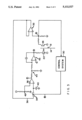
- FIG. 3 is a schematic diagram of illustrative circuitry for implementing the present invention.
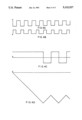
- FIGS. 4A-4D are timing charts useful for understanding the present invention, showing the signals appearing at the points A-D, respectively, in the circuit of FIG. 3.
- FIGS. 1 and 2 illustrates a motor 10 having an output shaft 12 on which is mounted for rotation therewith a reference generator disk 14.
- the disk 14 is diametrically divided into a first region 16 which is light transmissive and a second region 18 which is opaque.
- Straddling the disk 14 and fixed against rotation is an optical sensor assembly 20 which has a light emitting diode 22 (FIG. 3) in a first leg 24 and a phototransistor 26 (FIG. 3) in a second leg 28.
- the output of the phototransistor 26 at the point A is applied through the voltage follower 32 to the controllable switch 34.
- the switch 34 is controlled by the signal on the lead B from the control system 30 and, as shown in FIG. 4B, the switch trigger signal is a square wave signal which is active only during the time that light impinges on the phototransistor 26 and not during the transitions of the signal at the point A. Since the motor 10 operates at a substantially constant known speed, the control system 30 can generate the switch trigger signal on the lead B a preset time after the transition of the signal at the point A and terminate the switch trigger signal prior to the next transition of the signal at the point A.
- the switch 34 can be any type of controllable switch, such as, for example, an FET switch.
- the switch 34 When the switch 34 is closed, the signal on the lead 36 is applied as an input to the negative input terminal of the comparator 38.
- the switch 34 and the capacitor 40 operatively function as a sample and hold circuit so that the comparator 38 only sees the output of the phototransistor 26 during the time that light impinges thereon.
- the positive terminal input to the comparator 38 is obtained from the voltage divider 42 which provides a reference voltage corresponding to the desired output level of the phototransistor 26.
- the output of the comparator 38 passes through an attenuator network 44 to the input of an integrator network 46, the output of which is utilized to control the drive voltage across the light emitting diode 22.
- FIGS. 4A-4D for a description of the operation of the circuit shown in FIG. 3.
- the output of the integrator 46 at the point D is at zero. Therefore, the light emitting diode 22 has the maximum drive voltage applied thereacross and is at its brightest. Accordingly, the amplitude of the output of the photo-transistor 26 at the point A is at its maximum, which is greater than the reference level set by the voltage divider 42, so that the output of the comparator 38 at the point C is positive. This causes the integrator 46 output at the point D to ramp negatively, thereby decreasing the drive voltage across the light emitting diode 22 and dimming the output thereof.
- the output of the comparator 38 changes polarity and the integrator 46 output ramp reverses in slope, as shown in FIGS. 4C and 4D.
- a condition of stability is achieved where the output of the phototransistor 26 is maintained substantially at a desired predetermined fixed level. If temperature variations change the characteristics of the light emitting diode 22 and/or the phototransistor 26, the aforedescribed circuitry provides compensation for such changes.
Abstract
A compensation arrangement for an opto-electronic reference generator includes circuitry for comparing the output level from a light detector to a reference voltage and circuitry for utilizing the results of the comparison to control the drive voltage across a light emitter.
Description
This invention relates to opto-electronic reference generators and, more particularly, to an arrangement for providing a constant level output signal therefrom.
As described in U.S. Pat. No. 4,621,529, guidance systems for modern aircraft require rate and acceleration sensing. This may be achieved by utilizing a gyroscopic multi-sensor assembly which operates by sensing an angular velocity about some axis perpendicular to the spin bearing axis of the device with the use of a gyroscopic element. The gyroscopic element is mechanically restrained by a piezoelectric crystal beam so that gyroscopic reaction to angular velocity mechanically strains the piezoelectric crystal beam which in turn produces an electrical output signal proportional to angular velocity input. Similarly, a restrained piezoelectric crystal beam can be employed to sense linear acceleration along any axis perpendicular to the spin bearing axis. Thus, through the use of one or more mechanically restrained piezoelectric crystal beams, both the angular velocity and acceleration amplitude may be converted into electrical signals.
The spin bearing axis discussed above is defined by the rotational axis of the output shaft of a motor, upon which output shaft the gyroscopic element is mounted. In order to provide a reference signal which is required for timing purposes, a reference signal generator is also coupled to the motor output shaft. Such a reference signal generator may illustratively include a disk mounted for rotation on the output shaft, which disk is diametrically divided into a first region which is light transmissive and a second region which is opaque. The disk is then straddled by an optical sensing unit which includes a light emitting diode on one side of the disk and a phototransistor on the other side of the disk. Ideally, this sensor provides a square wave output.
While the aforedescribed arrangement operates generally satisfactorily, it will be appreciated that when mounted in an aircraft, the multi-sensor assembly is subjected to varying temperatures. Since the outputs of the light emitting diode and the phototransistor vary with temperature, such temperature variation results in a variation in the amplitude of the square wave output. In the particular system with which the present invention is concerned, the output of the phototransistor is provided as the input to a comparator circuit. There is a significant rise time at the output of the photo-transistor so that if the amplitude of the output varies, the relative triggering time of the comparator circuit will likewise vary. This is an undesirable condition.
It is therefore a primary object of the present invention to provide an arrangement wherein the amplitude of the phototransistor output signal is maintained at a substantially constant level independent of temperature.
The foregoing, and additional, objects are attained in accordance with the principles of this invention by comparing the output of the phototransistor with a reference voltage and controlling the drive voltage across the light emitting diode to maintain the photo-transistor output substantially at the reference voltage level.
In accordance with an aspect of this invention, sample and hold means are utilized to insure that the photo-transistor output comparison only takes place during the time that the light transmissive area of the disk is between the light emitting diode and the photo-transistor.
The foregoing will be more readily apparent upon reading the following description in conjunction with the drawings in which like elements in different figures thereof have the same reference numeral and wherein:
FIG. 1 is a perspective view schematically illustrating the reference generator assembly with which the present invention is concerned;
FIG. 2 is a side view of the assembly of FIG. 1;
FIG. 3 is a schematic diagram of illustrative circuitry for implementing the present invention; and
FIGS. 4A-4D are timing charts useful for understanding the present invention, showing the signals appearing at the points A-D, respectively, in the circuit of FIG. 3.
Referring now to the drawings, FIGS. 1 and 2 illustrates a motor 10 having an output shaft 12 on which is mounted for rotation therewith a reference generator disk 14. The disk 14 is diametrically divided into a first region 16 which is light transmissive and a second region 18 which is opaque. Straddling the disk 14 and fixed against rotation is an optical sensor assembly 20 which has a light emitting diode 22 (FIG. 3) in a first leg 24 and a phototransistor 26 (FIG. 3) in a second leg 28.
Referring now to FIG. 3, light produced by the light emitting diode 22 passes through the disk 14 and impinges on the phototransistor 26 when the light transmissive region 16 is therebetween. This causes the phototransistor 26 to become conductive, to an extent which depends upon the amount of light impinging thereon, so as to lower the voltage at the point A. When the opaque region 18 of the disk 14 is between the light emitting diode 22 and the phototransistor 26, the photo-transistor 26 becomes non-conductive, raising the voltage at the point A. Thus, the voltage at the point A ideally takes the form of a square wave (FIG. 4A). This square wave is utilized by the control system 30 as a reference signal to provide timing for the multi-sensor system. As described above, when the system is subjected to temperature variation, the amplitude of the square wave at the point A will vary. The present invention compensates for such variation, as will be described below.
The output of the phototransistor 26 at the point A is applied through the voltage follower 32 to the controllable switch 34. The switch 34 is controlled by the signal on the lead B from the control system 30 and, as shown in FIG. 4B, the switch trigger signal is a square wave signal which is active only during the time that light impinges on the phototransistor 26 and not during the transitions of the signal at the point A. Since the motor 10 operates at a substantially constant known speed, the control system 30 can generate the switch trigger signal on the lead B a preset time after the transition of the signal at the point A and terminate the switch trigger signal prior to the next transition of the signal at the point A.
The switch 34, while shown schematically in FIG. 3, can be any type of controllable switch, such as, for example, an FET switch. When the switch 34 is closed, the signal on the lead 36 is applied as an input to the negative input terminal of the comparator 38. The switch 34 and the capacitor 40 operatively function as a sample and hold circuit so that the comparator 38 only sees the output of the phototransistor 26 during the time that light impinges thereon. The positive terminal input to the comparator 38 is obtained from the voltage divider 42 which provides a reference voltage corresponding to the desired output level of the phototransistor 26.
The output of the comparator 38 passes through an attenuator network 44 to the input of an integrator network 46, the output of which is utilized to control the drive voltage across the light emitting diode 22.
Reference is now made to FIGS. 4A-4D for a description of the operation of the circuit shown in FIG. 3. When the circuit is first turned on, the output of the integrator 46 at the point D is at zero. Therefore, the light emitting diode 22 has the maximum drive voltage applied thereacross and is at its brightest. Accordingly, the amplitude of the output of the photo-transistor 26 at the point A is at its maximum, which is greater than the reference level set by the voltage divider 42, so that the output of the comparator 38 at the point C is positive. This causes the integrator 46 output at the point D to ramp negatively, thereby decreasing the drive voltage across the light emitting diode 22 and dimming the output thereof. When the light emitting diode 22 is sufficiently dim that the amplitude of the signal at the output of the phototransistor 26 is less than the desired level, the output of the comparator 38 changes polarity and the integrator 46 output ramp reverses in slope, as shown in FIGS. 4C and 4D. Thus, a condition of stability is achieved where the output of the phototransistor 26 is maintained substantially at a desired predetermined fixed level. If temperature variations change the characteristics of the light emitting diode 22 and/or the phototransistor 26, the aforedescribed circuitry provides compensation for such changes.
Accordingly, there has been disclosed a compensation arrangement for an opto-electronic reference generator. While an illustrative embodiment of the present invention has been disclosed herein, it will be apparent to those of ordinary skill in the art that various modifications and adaptations to that embodiment are possible and it is only intended that the present invention be limited by the scope of the appended claims.
Claims (6)
1. In a system having a moving element of alternating light transmissive and opaque areas, a controllable light emitting device situated on a first side of said moving element, a light detecting device situated on a second side of said moving element opposite said light emitting device and adapted to receive light from said light emitting device when a light transmissive area of said moving element is between said devices, said light detecting device providing a first signal representative of the amount of light impinging thereon, and means utilizing said first signal for providing a reference signal indicative of the position of said moving element relative to said light emitting and detecting devices, an arrangement for maintaining the level of said first signal substantially at a predetermined fixed level when light from said light emitting device passes through a light transmissive area of said moving element and impinges on said light detecting device, the arrangement comprising:
means for providing a reference voltage corresponding to said predetermined fixed level;
means for providing a second signal corresponding to said first signal where the correspondence between said first and second signals is the same as the correspondence between said fixed level and said reference voltage;
means for comparing said second signal with said reference voltage and providing a comparison signal representative of the difference therebetween; and
means for utilizing said comparison signal to provide a variable drive voltage across said light emitting device so as to maintain the level of said first signal substantially at said predetermined fixed level when light from said light emitting device passes through a light transmissive area of said moving element and impinges on said light detecting device, the light produced by said light emitting device being related to the magnitude of said drive voltage.
2. The arrangement according to claim 1 wherein said comparing means includes sample and hold means operating in synchronism with said reference signal and coupled to receive said second signal for insuring that the comparing of said second signal with said reference voltage uses the level of said second signal only when a light transmissive area of said moving element is between said light emitting and detecting devices.
3. The arrangement according to claim 1 wherein said light emitting device comprises a light emitting diode having first and second terminals, and said utilizing means includes:
means for coupling said first terminal to a fixed supply voltage; and
integrating means coupled between said comparing means and said second terminal for varying the drive voltage across said light emitting diode in accordance with said comparison signal.
4. The arrangement according to claim 3 wherein said comparing means includes sample and hold means operating in synchronism with said reference signal and coupled to receive said second signal for insuring that the comparing of said second signal with said reference voltage uses the level of said second signal only when a light transmissive area of said moving element is between said light emitting and detecting devices.
5. The arrangement according to claim 4 wherein said comparing means further includes a comparator having first and second inputs and an output, said reference voltage being coupled to said first input and said sample and hold means being coupled to said second input, said output being coupled to said integrating means.
6. The arrangement according to claim 5 further including an attenuator coupled between said comparator output and said integrating means.
Priority Applications (3)
| Application Number | Priority Date | Filing Date | Title |
|---|---|---|---|
| US07/710,373 US5132527A (en) | 1991-05-30 | 1991-05-30 | Compensation arrangement for opto-electronic reference generator |
| GB919124243A GB9124243D0 (en) | 1991-05-30 | 1991-11-14 | Compensation arrangement for opto-electronic reference generator |
| JP3338670A JPH0529883A (en) | 1991-05-30 | 1991-12-20 | Compensator for optical electronic reference generator |
Applications Claiming Priority (1)
| Application Number | Priority Date | Filing Date | Title |
|---|---|---|---|
| US07/710,373 US5132527A (en) | 1991-05-30 | 1991-05-30 | Compensation arrangement for opto-electronic reference generator |
Publications (1)
| Publication Number | Publication Date |
|---|---|
| US5132527A true US5132527A (en) | 1992-07-21 |
Family
ID=24853782
Family Applications (1)
| Application Number | Title | Priority Date | Filing Date |
|---|---|---|---|
| US07/710,373 Expired - Fee Related US5132527A (en) | 1991-05-30 | 1991-05-30 | Compensation arrangement for opto-electronic reference generator |
Country Status (3)
| Country | Link |
|---|---|
| US (1) | US5132527A (en) |
| JP (1) | JPH0529883A (en) |
| GB (1) | GB9124243D0 (en) |
Cited By (10)
| Publication number | Priority date | Publication date | Assignee | Title |
|---|---|---|---|---|
| US5285058A (en) * | 1993-01-14 | 1994-02-08 | Schlumberger Industries, Inc. | Optical sensor control including the suspension of light radiation |
| US5610394A (en) * | 1996-04-29 | 1997-03-11 | Itron, Inc. | Rotation monitor disturbance neutralization system |
| US5798670A (en) * | 1996-04-29 | 1998-08-25 | Itron, Inc. | Active filter circuit |
| US6107620A (en) * | 1996-01-09 | 2000-08-22 | Canon Kabushiki Kaisha | Photosensor using side surface light |
| GB2347210A (en) * | 1999-02-26 | 2000-08-30 | Infrared Eng | Electro-magnetic detection apparatus |
| US20070119933A1 (en) * | 2005-11-28 | 2007-05-31 | Chin Yee L | Optical encoder with contamination detection |
| US8184974B2 (en) | 2006-09-11 | 2012-05-22 | Lumexis Corporation | Fiber-to-the-seat (FTTS) fiber distribution system |
| US8416698B2 (en) | 2009-08-20 | 2013-04-09 | Lumexis Corporation | Serial networking fiber optic inflight entertainment system network configuration |
| US8424045B2 (en) | 2009-08-14 | 2013-04-16 | Lumexis Corporation | Video display unit docking assembly for fiber-to-the-screen inflight entertainment system |
| US8659990B2 (en) | 2009-08-06 | 2014-02-25 | Lumexis Corporation | Serial networking fiber-to-the-seat inflight entertainment system |
Citations (3)
| Publication number | Priority date | Publication date | Assignee | Title |
|---|---|---|---|---|
| US4074128A (en) * | 1976-05-05 | 1978-02-14 | General Electric Company | Photoelectric signal generating circuits |
| US4203032A (en) * | 1977-08-04 | 1980-05-13 | Siemens Aktiengesellschaft | Arrangement for producing a constant signal amplitude in an opto-electronic scanning system |
| US5043565A (en) * | 1985-12-11 | 1991-08-27 | Deutsche Thomson-Brandt Gmbh | Process and circuit for compensating changes |
Family Cites Families (2)
| Publication number | Priority date | Publication date | Assignee | Title |
|---|---|---|---|---|
| JPS5118864A (en) * | 1974-08-06 | 1976-02-14 | Matsushita Electric Works Ltd | TAIKOSHIKIKO DENSUITSUCHI |
| JPS5231189A (en) * | 1975-09-04 | 1977-03-09 | Unitika Ltd | Two tone pattern dyeing method of synthetic long fiber woven products |
-
1991
- 1991-05-30 US US07/710,373 patent/US5132527A/en not_active Expired - Fee Related
- 1991-11-14 GB GB919124243A patent/GB9124243D0/en active Pending
- 1991-12-20 JP JP3338670A patent/JPH0529883A/en active Pending
Patent Citations (3)
| Publication number | Priority date | Publication date | Assignee | Title |
|---|---|---|---|---|
| US4074128A (en) * | 1976-05-05 | 1978-02-14 | General Electric Company | Photoelectric signal generating circuits |
| US4203032A (en) * | 1977-08-04 | 1980-05-13 | Siemens Aktiengesellschaft | Arrangement for producing a constant signal amplitude in an opto-electronic scanning system |
| US5043565A (en) * | 1985-12-11 | 1991-08-27 | Deutsche Thomson-Brandt Gmbh | Process and circuit for compensating changes |
Cited By (16)
| Publication number | Priority date | Publication date | Assignee | Title |
|---|---|---|---|---|
| US5285058A (en) * | 1993-01-14 | 1994-02-08 | Schlumberger Industries, Inc. | Optical sensor control including the suspension of light radiation |
| US6107620A (en) * | 1996-01-09 | 2000-08-22 | Canon Kabushiki Kaisha | Photosensor using side surface light |
| US5610394A (en) * | 1996-04-29 | 1997-03-11 | Itron, Inc. | Rotation monitor disturbance neutralization system |
| US5798670A (en) * | 1996-04-29 | 1998-08-25 | Itron, Inc. | Active filter circuit |
| GB2347210A (en) * | 1999-02-26 | 2000-08-30 | Infrared Eng | Electro-magnetic detection apparatus |
| GB2347210B (en) * | 1999-02-26 | 2003-08-06 | Infrared Eng | Infrared gauge |
| US20070119933A1 (en) * | 2005-11-28 | 2007-05-31 | Chin Yee L | Optical encoder with contamination detection |
| US7845556B2 (en) * | 2005-11-28 | 2010-12-07 | Avago Technologies Ecbu Ip (Singapore) Pte. Ltd. | Optical encoder with contamination detection |
| US8184974B2 (en) | 2006-09-11 | 2012-05-22 | Lumexis Corporation | Fiber-to-the-seat (FTTS) fiber distribution system |
| US8659990B2 (en) | 2009-08-06 | 2014-02-25 | Lumexis Corporation | Serial networking fiber-to-the-seat inflight entertainment system |
| US9118547B2 (en) | 2009-08-06 | 2015-08-25 | Lumexis Corporation | Serial networking fiber-to-the-seat inflight entertainment system |
| US9532082B2 (en) | 2009-08-06 | 2016-12-27 | Lumexis Corporation | Serial networking fiber-to-the-seat inflight entertainment system |
| US8424045B2 (en) | 2009-08-14 | 2013-04-16 | Lumexis Corporation | Video display unit docking assembly for fiber-to-the-screen inflight entertainment system |
| US8416698B2 (en) | 2009-08-20 | 2013-04-09 | Lumexis Corporation | Serial networking fiber optic inflight entertainment system network configuration |
| US9036487B2 (en) | 2009-08-20 | 2015-05-19 | Lumexis Corporation | Serial networking fiber optic inflight entertainment system network configuration |
| US9344351B2 (en) | 2009-08-20 | 2016-05-17 | Lumexis Corporation | Inflight entertainment system network configurations |
Also Published As
| Publication number | Publication date |
|---|---|
| GB9124243D0 (en) | 1992-01-08 |
| JPH0529883A (en) | 1993-02-05 |
Similar Documents
| Publication | Publication Date | Title |
|---|---|---|
| US5132527A (en) | Compensation arrangement for opto-electronic reference generator | |
| EP0370963B1 (en) | Circuit for an electromagnetic rotation sensor | |
| US4156169A (en) | Servo control apparatus | |
| GB1588024A (en) | Hysteresis synchronous motor speed servo system | |
| US4160200A (en) | Servo control apparatus | |
| US4437047A (en) | System for autonomous earth-pointing acquisition of a dual-spin satellite | |
| US4366422A (en) | Velocity sensing pulse pair servo apparatus | |
| US4947033A (en) | Voltage/frequency converter and its use in an optical wave guide transmission arrangement | |
| US4594540A (en) | Angular measurement system | |
| US4430606A (en) | Sheet feeding apparatus | |
| US3945037A (en) | Feedback control system for linear position transducer | |
| US4109190A (en) | Circuit for increasing the operating speed range of a velocity servo system | |
| US3665282A (en) | Scan control system | |
| EP0166699B1 (en) | Circuit for detecting the passage through zero of the signal generated by an electromagnetic sensor of the phonic wheel type | |
| US6144229A (en) | Sensor device | |
| US4144753A (en) | Circuit arrangement for determining physical parameters of flowing media by the ultrasonic method | |
| US4644188A (en) | Voltage comparison circuits for motion amplitude regulators or the like | |
| US3844168A (en) | Torque measuring apparatus | |
| US4499436A (en) | Motion amplitude regulator with breaking pulse regulation | |
| US3329824A (en) | Photoelectric print reading circuit | |
| US4016471A (en) | Level detection system having a band-pass characteristic and a servo system including the same | |
| CA2023338A1 (en) | Optical disk device eliminating offset of actuator and offset eliminating method used thereby | |
| JP2579970B2 (en) | Rotation control device | |
| SU1023278A2 (en) | Piezo motor displacement automatic control (its versions) | |
| US5305629A (en) | Regulated negative calibration pulse generator |
Legal Events
| Date | Code | Title | Description |
|---|---|---|---|
| AS | Assignment |
Owner name: GEC-MARCONI ELECTRONIC SYSTEMS CORPORATION, A CORP Free format text: ASSIGNMENT OF ASSIGNORS INTEREST.;ASSIGNOR:KARPATI, ANTHONY J.;REEL/FRAME:005745/0573 Effective date: 19910523 |
|
| DD | Disclaimer and dedication filed |
Free format text: 920803 |
|
| REMI | Maintenance fee reminder mailed | ||
| LAPS | Lapse for failure to pay maintenance fees | ||
| FP | Expired due to failure to pay maintenance fee |
Effective date: 19960724 |
|
| STCH | Information on status: patent discontinuation |
Free format text: PATENT EXPIRED DUE TO NONPAYMENT OF MAINTENANCE FEES UNDER 37 CFR 1.362 |