US5185056A - Method and apparatus for etching semiconductor wafers and developing resists - Google Patents
Method and apparatus for etching semiconductor wafers and developing resists Download PDFInfo
- Publication number
- US5185056A US5185056A US07/759,277 US75927791A US5185056A US 5185056 A US5185056 A US 5185056A US 75927791 A US75927791 A US 75927791A US 5185056 A US5185056 A US 5185056A
- Authority
- US
- United States
- Prior art keywords
- wafer
- modifying
- fluid
- etching
- modifying fluid
- Prior art date
- Legal status (The legal status is an assumption and is not a legal conclusion. Google has not performed a legal analysis and makes no representation as to the accuracy of the status listed.)
- Expired - Fee Related
Links
Images
Classifications
-
- H—ELECTRICITY
- H01—ELECTRIC ELEMENTS
- H01L—SEMICONDUCTOR DEVICES NOT COVERED BY CLASS H10
- H01L21/00—Processes or apparatus adapted for the manufacture or treatment of semiconductor or solid state devices or of parts thereof
- H01L21/67—Apparatus specially adapted for handling semiconductor or electric solid state devices during manufacture or treatment thereof; Apparatus specially adapted for handling wafers during manufacture or treatment of semiconductor or electric solid state devices or components ; Apparatus not specifically provided for elsewhere
- H01L21/67005—Apparatus not specifically provided for elsewhere
- H01L21/67011—Apparatus for manufacture or treatment
- H01L21/67017—Apparatus for fluid treatment
- H01L21/67063—Apparatus for fluid treatment for etching
- H01L21/67075—Apparatus for fluid treatment for etching for wet etching
- H01L21/6708—Apparatus for fluid treatment for etching for wet etching using mainly spraying means, e.g. nozzles
-
- H—ELECTRICITY
- H01—ELECTRIC ELEMENTS
- H01L—SEMICONDUCTOR DEVICES NOT COVERED BY CLASS H10
- H01L21/00—Processes or apparatus adapted for the manufacture or treatment of semiconductor or solid state devices or of parts thereof
- H01L21/67—Apparatus specially adapted for handling semiconductor or electric solid state devices during manufacture or treatment thereof; Apparatus specially adapted for handling wafers during manufacture or treatment of semiconductor or electric solid state devices or components ; Apparatus not specifically provided for elsewhere
- H01L21/67005—Apparatus not specifically provided for elsewhere
- H01L21/67011—Apparatus for manufacture or treatment
- H01L21/67017—Apparatus for fluid treatment
- H01L21/67063—Apparatus for fluid treatment for etching
- H01L21/67075—Apparatus for fluid treatment for etching for wet etching
Definitions
- the present invention relates to method and apparatus for etching a semiconductor substrate and more particularly to a method and apparatus for etching a semiconductor substrate wherein etching fluid is moved across selected areas of the substrate by dynamic force.
- U.S. Pat. No. 3,041,225 issued Jun. 26, 1932 to Emeis and entitled METHOD AND APPARATUS FOR SURFACE TREATMENT OF P-N JUNCTION SEMICONDUCTORS describes a structure which utilizes centrifugal force for increasing the flow velocity of the etching liquid by rotating a wafer member during processing about an axis normal to the surface being etched. During rotation, the etching liquid, supplied in form of a free jet, is flung outwardly by centrifugal force.
- a nozzle shaped tube is positioned above a rotating disc containing a wafer. An etching liquid is thereby directed onto the wafer. Centrifugal force is imposed upon the etching fluid by the rotation of the disc.
- U.S. Pat. No. 3,674,579, issued Jul. 4, 1972 to Clinehens et al entitled METHOD OF FORMING ELECTRICAL CONDUCTORS relates to a method of forming electrical conductors to selected regions of a semiconductor wafer.
- An aluminum film of approximately 10,000 angstroms is evaporated upon a silicon dioxide insulative evaporation mask which has been formed on a silicon wafer.
- a conductor mask is formed upon selected areas of the aluminum film.
- the masked aluminum film is placed upon a spinner. Phosphoric acid is continuously poured near the center of the masked metal film.
- the masked aluminum film is spun for a period of approximately four minutes, to remove the portions of the aluminum film which are not coated by the conductor mask, in order to form electrical conductors in contact with selected regions of the silicon wafer.
- U.S. Pat. No. 3,953,265, issued Apr. 27, 1976 to Hood entitled MENISCUS-CONTAINED METHOD OF HANDLING FLUIDS IN THE MANUFACTURE OF SEMICONDUCTOR WAFERS relates to a method for reducing the consumption of etchants used in manufacturing semiconductor devices comprising the steps of supporting a semiconductor wafer, metering a predetermined volume of etchant onto the surface of said wafer to form a meniscus-contained body of etchant thereon, maintaining said wafer static during etching, sensing the completion of said etching, and spinning said wafer upon completion of the etching to remove the etchant from the wafer and terminate the etching operation.
- U.S. Pat. No. 4,339,297 issued Jul. 13, 1982 to Aigo entitled APPARATUS FOR ETCHING OF OXIDE FILM ON SEMICONDUCTOR WAFER, discloses an apparatus for applying photo-etching on one surface of a semiconductor wafer formed with oxide film is provided, which comprises a cup-shaped basin having at the bottom thereof a vertical passage for introducing etching liquid, and a chuck rotatably supported above said basin for vacuum-absorbing a semiconductor wafer at the bottom surface thereof, said one surface of wafer facing downward being contacted with etching liquid that is blown up vertically through said vertical passage of the basin, to thereby prevent the upward facing rear surface of wafer from being contacted with etching liquid to hold oxide film thereon, and means for rotating said chuck to remove any reaction gas resulted on said one surface of wafer.
- U.S. Pat. No. 4,544,446, issued Oct. 1, 1985 to Cady entitled VLSI CHEMICAL REACTOR discloses a VLSI chemical reactor that includes a fluid flow guide spaced from the corresponding substrate in the form of a wafer for significantly reducing contamination in the processing of semiconductor wafers. Processing chemicals are introduced in a continuous process through a central tube and through the fluid flow guide which is substantially planar and which is parallel to the surface of the wafer. A predetermined gap is maintained between the guide and the wafer such that fluid is maintained in the gap at all times critical in the processing of the wafer.
- An object of the present invention is to provide a system for etching a wafer surface or developing a resist on a wafer surface wherein the etchant or developer is applied to the surface of the wafer or the resist in a liquid pool over the area to be etched or developed by means of a delivery nozzle and the wafer is mounted on a rotating turntable where a vacuum nozzle is disposed at the circumference of the etchant pool or developer.
- Another object of the invention is to provide a method for the described system wherein as the turntable is rotated, the etchant or developer removes or develops the wafer region or the resist region on the wafer and centrifugal force causes the etchant or developer to move to the vacuum nozzle where it is continually removed.
- a further object of the present invention is to provide a system and method as disclosed in which the vacuum nozzle is disposed on the end of a radial arm attached to a radial position and wherein the desired diameter of the etch is controlled by the position of the arm.
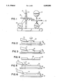
- FIG. 1 is a schematic illustration of an embodiment of an etching system for semiconductor wafers.
- FIGS. 2, 3 and 4 illustrate the use of the apparatus illustrated in FIG. 1 for the fabrication of a membrane.
- FIGS. 5 and 6 illustrate the use of the apparatus of FIG. 1 for selectively clearing or developing resist.
- Membranes on silicon wafers are widely used, for example, as masks in X-ray lithography systems.
- the membrane material In order to back-etch silicon wafers to fabricate a membrane out of the material grown, deposited or diffused-in on the front side of the wafer, the membrane material has to withstand the etchant or it has to be protected from it.
- a suitable resist organic or inorganic
- the wafer would have to be held in an appropriate fixture to provide similar protection.
- the back side protection would have to be built-in, as is the case of B-doped Si.
- the wafer has to be able to withstand planar etching (i.e., etching of the whole defined section all at once until the membrane if formed all at the same time) and the membrane has to be able to withstand all of the above and the associated process steps to deposit and remove the resist, etc.
- planar etching i.e., etching of the whole defined section all at once until the membrane if formed all at the same time
- wafers that are found to be under stress may not withstand a planar etch process. Conventional bath etching will result in the destruction of such samples.
- the present invention provides improved apparatus and method for producing a membrane.
- the method and apparatus are gentle enough as to also provide some relief in cases when the membrane material is very thin or fragile, as compared with conventional planar etch processes.
- Such processes also require additional steps for resist application, patterning, removal, and cleaning of the membrane. The absence of the need for such additional steps results in increased ease of use, versatility and sample yield.
- the method of the present invention consists of a succession of radial etch steps. Beginning, typically, at the center of the sample, an etch well is expanded radially outwards keeping a steep slope on the well walls. Alternatively, for samples where catastrophic stress relief is not a problem, the area to be etched can be defined and etched all at once. The etchant is added to the center of the sample and suctioned around the periphery of the well.
- Any suitable etchant can be used with this method, specially advantageous are fast etchants. Strong mixtures of hydrofluoric, nitric and acetic (or water) are particularly useful for silicon, however, different etchants or mixtures thereof can be used for different stages of the etching process (i.e., bulk etching vs. edge finishing).
- the structure illustrated in FIG. 1 is employed.
- the structure includes a turntable 10, movable arm 12, etchant delivery nozzle 14, reservoir (or pump) 16 and sensors.
- Movable suction arm 12 can be raised or lowered in the Z direction by a motor driven vertical positioner 20 mounted on support 22. Suction arm 12 can also be positioned at points from the center of turntable 10 radially outward to the circumference of turntable 10 by a radial positioner 24 driven by motor 26.
- Etchant is delivered onto the wafer by nozzle 14 at an appropriate rate and location.
- the etchant is delivered at the center of the wafer (the center of rotation).
- the pool of etchant expands outward due to centrifugal force as it etches the wafer.
- the suction arm 12 is located at a selected radial distance in accordance with the desired membrane diameter. The suction arm 12 removes the etchant away from the wafer at the desired radial distance such that the remaining portion radially further than suction arm 12 is not etched.
- the nozzle 14 may be moved with respect to the turntable 10, the suction arm 12 may be moved with respect to a fixed turntable 10 location, turntable 10 may be moved with respect to a fixed suction arm 12, or combination of the above. Also, multiple suction arms positioned over the turntable 10 as well as multiple nozzles may also be employed.
- the etchant is administered to the sample via the nozzle at an appropriate rate and location.
- the area to be etched is defined by the position of the movable arm, which suctions the etchant away from the sample. Typically, a small area is etched all the way through the wafer and expanded outwards (by moving the arm) to reach the desired membrane diameter. The rate of expansion determined by the etchant, sample geometry and stress state, among other things.
- the method and apparatus solve a major problem in back-etching wafers for the fabrication of membranes for X-ray mask applications. It has been shown to be particularly useful in silicon/silicon carbide systems where spurious carbide deposition on the back of the wafers prevents adhesion of protective layers. Even of greater importance is the fact that the system allows the etching of highly stressed wafers, that would be very hard to etch in any other way. Also, the system is ideally suited for small runs and does not require the large volume etching tanks typically needed for bath etching. Etchants can be changed during the process without interruption or without removing the samples. Diamond or diamond-like materials grown on silicon have also greatly benefited from this method of membrane formation.
- the system can detect the onset of different stages during the etching process by including a variety of sensors in the structure of FIG. 1. Included are initial etch-trough, position and end-point.
- the process can be totally automated and be made compatible with standard manufacturing interfaces by appropriate use of robotics.
- FIG. 2 shows turntable 10 having therein a wafer 28 on the back of which is a deposited film 30 which will become a membrane.
- a pool of etchant 32 has been delivered by the nozzle shown in FIG. 1, and as turntable 10 rotates the etchant is forced outwardly to the location in FIG. 2 where suction arm 12 is located.
- Suction arm 12 removes the etchant 32 at this location, such that the wafer 28 is etched at a selected area and diameter as shown in FIG. 3.
- the etchant removes all the wafer 28 material within the area defined by the nozzle, leaving only the membrane 30 as shown in FIG. 4.
- the etching depth is detected by known sensors and known techniques, and the etching is terminated as desired.
- the described apparatus and method may be used to develop a resist layer on a wafer surface instead of etching the wafer surface.
- a wafer 28 is located on turntable 10 which has a layer of resist 34 on the front side thereof.
- the turntable 10 is shown having an offset center of rotation.
- the developer is delivered to the desired point, i.e., the center of rotation and nozzle 12 is disposed at the desired diameter distance.
- the etchant selectively clears or develops the resist in a predetermined area.
Abstract
Description
Claims (13)
Priority Applications (1)
| Application Number | Priority Date | Filing Date | Title |
|---|---|---|---|
| US07/759,277 US5185056A (en) | 1991-09-13 | 1991-09-13 | Method and apparatus for etching semiconductor wafers and developing resists |
Applications Claiming Priority (1)
| Application Number | Priority Date | Filing Date | Title |
|---|---|---|---|
| US07/759,277 US5185056A (en) | 1991-09-13 | 1991-09-13 | Method and apparatus for etching semiconductor wafers and developing resists |
Publications (1)
| Publication Number | Publication Date |
|---|---|
| US5185056A true US5185056A (en) | 1993-02-09 |
Family
ID=25055062
Family Applications (1)
| Application Number | Title | Priority Date | Filing Date |
|---|---|---|---|
| US07/759,277 Expired - Fee Related US5185056A (en) | 1991-09-13 | 1991-09-13 | Method and apparatus for etching semiconductor wafers and developing resists |
Country Status (1)
| Country | Link |
|---|---|
| US (1) | US5185056A (en) |
Cited By (11)
| Publication number | Priority date | Publication date | Assignee | Title |
|---|---|---|---|---|
| US5634980A (en) * | 1993-03-31 | 1997-06-03 | Sony Corporation | Method for washing substrates |
| US5705318A (en) * | 1994-06-06 | 1998-01-06 | Case Western Reserve University | Micromotors and methods of fabrication |
| US5759335A (en) * | 1996-12-26 | 1998-06-02 | Samsung Electronics Co., Ltd. | Photoresist removing apparatus |
| US5788468A (en) * | 1994-11-03 | 1998-08-04 | Memstek Products, Llc | Microfabricated fluidic devices |
| US5993681A (en) * | 1998-05-08 | 1999-11-30 | Lucent Technology, Inc. | Method and apparatus for aiming a spray etcher nozzle |
| US6029337A (en) * | 1994-06-06 | 2000-02-29 | Case Western Reserve University | Methods of fabricating micromotors with utilitarian features |
| US6153532A (en) * | 1998-02-27 | 2000-11-28 | Micron Technology, Inc. | Methods and apparatuses for removing material from discrete areas on a semiconductor wafer |
| US6360424B1 (en) | 1994-06-06 | 2002-03-26 | Case Western Reserve University | Method of making micromotors with utilitarian features |
| US6497240B1 (en) * | 1999-04-21 | 2002-12-24 | Sharp Kabushiki Kaisha | Ultrasound cleaning device and resist-stripping device |
| US20030121538A1 (en) * | 1997-08-20 | 2003-07-03 | Zahorik Russell C. | Apparatus for selective removal of material from wafer alignment marks |
| CN116107156A (en) * | 2023-04-11 | 2023-05-12 | 深圳市龙图光罩股份有限公司 | Mask etching equipment, method and system and computer readable storage medium |
Citations (11)
| Publication number | Priority date | Publication date | Assignee | Title |
|---|---|---|---|---|
| US2568803A (en) * | 1949-06-09 | 1951-09-25 | Guenst William | Etching machine |
| US3041225A (en) * | 1958-06-18 | 1962-06-26 | Siemens Ag | Method and apparatus for surface treatment of p-n junction semiconductors |
| US3597289A (en) * | 1967-01-19 | 1971-08-03 | Licentia Gmbh | Method of etching a semiconductor body |
| US3674579A (en) * | 1970-07-02 | 1972-07-04 | Ncr Co | Method of forming electrical conductors |
| US3953265A (en) * | 1975-04-28 | 1976-04-27 | International Business Machines Corporation | Meniscus-contained method of handling fluids in the manufacture of semiconductor wafers |
| US4161356A (en) * | 1977-01-21 | 1979-07-17 | Burchard John S | Apparatus for in-situ processing of photoplates |
| US4339297A (en) * | 1981-04-14 | 1982-07-13 | Seiichiro Aigo | Apparatus for etching of oxide film on semiconductor wafer |
| US4344809A (en) * | 1980-09-29 | 1982-08-17 | Wensink Ben L | Jet etch apparatus for decapsulation of molded devices |
| US4350562A (en) * | 1980-07-23 | 1982-09-21 | Siemens Aktiengesellschaft | Method for etching semiconductor wafers on one side |
| US4544446A (en) * | 1984-07-24 | 1985-10-01 | J. T. Baker Chemical Co. | VLSI chemical reactor |
| US5001084A (en) * | 1986-11-27 | 1991-03-19 | Mitsubishi Denki Kabushiki Kaisha | Method for applying a treatment liquid on a semiconductor wafer |
-
1991
- 1991-09-13 US US07/759,277 patent/US5185056A/en not_active Expired - Fee Related
Patent Citations (11)
| Publication number | Priority date | Publication date | Assignee | Title |
|---|---|---|---|---|
| US2568803A (en) * | 1949-06-09 | 1951-09-25 | Guenst William | Etching machine |
| US3041225A (en) * | 1958-06-18 | 1962-06-26 | Siemens Ag | Method and apparatus for surface treatment of p-n junction semiconductors |
| US3597289A (en) * | 1967-01-19 | 1971-08-03 | Licentia Gmbh | Method of etching a semiconductor body |
| US3674579A (en) * | 1970-07-02 | 1972-07-04 | Ncr Co | Method of forming electrical conductors |
| US3953265A (en) * | 1975-04-28 | 1976-04-27 | International Business Machines Corporation | Meniscus-contained method of handling fluids in the manufacture of semiconductor wafers |
| US4161356A (en) * | 1977-01-21 | 1979-07-17 | Burchard John S | Apparatus for in-situ processing of photoplates |
| US4350562A (en) * | 1980-07-23 | 1982-09-21 | Siemens Aktiengesellschaft | Method for etching semiconductor wafers on one side |
| US4344809A (en) * | 1980-09-29 | 1982-08-17 | Wensink Ben L | Jet etch apparatus for decapsulation of molded devices |
| US4339297A (en) * | 1981-04-14 | 1982-07-13 | Seiichiro Aigo | Apparatus for etching of oxide film on semiconductor wafer |
| US4544446A (en) * | 1984-07-24 | 1985-10-01 | J. T. Baker Chemical Co. | VLSI chemical reactor |
| US5001084A (en) * | 1986-11-27 | 1991-03-19 | Mitsubishi Denki Kabushiki Kaisha | Method for applying a treatment liquid on a semiconductor wafer |
Cited By (19)
| Publication number | Priority date | Publication date | Assignee | Title |
|---|---|---|---|---|
| US5634980A (en) * | 1993-03-31 | 1997-06-03 | Sony Corporation | Method for washing substrates |
| US6360424B1 (en) | 1994-06-06 | 2002-03-26 | Case Western Reserve University | Method of making micromotors with utilitarian features |
| US5705318A (en) * | 1994-06-06 | 1998-01-06 | Case Western Reserve University | Micromotors and methods of fabrication |
| US6029337A (en) * | 1994-06-06 | 2000-02-29 | Case Western Reserve University | Methods of fabricating micromotors with utilitarian features |
| US5788468A (en) * | 1994-11-03 | 1998-08-04 | Memstek Products, Llc | Microfabricated fluidic devices |
| US5759335A (en) * | 1996-12-26 | 1998-06-02 | Samsung Electronics Co., Ltd. | Photoresist removing apparatus |
| US20070207613A1 (en) * | 1997-08-20 | 2007-09-06 | Zahorik Russell C | Methods for selective removal of material from wafer alignment marks |
| US20040038543A1 (en) * | 1997-08-20 | 2004-02-26 | Zahorik Russell C. | Methods for selective removal of material from wafer alignment marks |
| US8053371B2 (en) | 1997-08-20 | 2011-11-08 | Micron Technology, Inc. | Apparatus and methods for selective removal of material from wafer alignment marks |
| US7244681B2 (en) | 1997-08-20 | 2007-07-17 | Micron Technology, Inc. | Methods for selective removal of material from wafer alignment marks |
| US6889698B2 (en) | 1997-08-20 | 2005-05-10 | Micron Technology, Inc. | Apparatus for selective removal of material from wafer alignment marks |
| US20030121538A1 (en) * | 1997-08-20 | 2003-07-03 | Zahorik Russell C. | Apparatus for selective removal of material from wafer alignment marks |
| US6610610B2 (en) * | 1997-08-20 | 2003-08-26 | Micron Technology, Inc. | Methods for selective removal of material from wafer alignment marks |
| US6376390B1 (en) | 1998-02-27 | 2002-04-23 | Micron Technology, Inc. | Methods and apparatuses for removing material from discrete areas on a semiconductor wafer |
| US6375792B1 (en) * | 1998-02-27 | 2002-04-23 | Micron Technology, Inc. | Methods and apparatuses for removing material from discrete areas on a semiconductor wafer |
| US6153532A (en) * | 1998-02-27 | 2000-11-28 | Micron Technology, Inc. | Methods and apparatuses for removing material from discrete areas on a semiconductor wafer |
| US5993681A (en) * | 1998-05-08 | 1999-11-30 | Lucent Technology, Inc. | Method and apparatus for aiming a spray etcher nozzle |
| US6497240B1 (en) * | 1999-04-21 | 2002-12-24 | Sharp Kabushiki Kaisha | Ultrasound cleaning device and resist-stripping device |
| CN116107156A (en) * | 2023-04-11 | 2023-05-12 | 深圳市龙图光罩股份有限公司 | Mask etching equipment, method and system and computer readable storage medium |
Similar Documents
| Publication | Publication Date | Title |
|---|---|---|
| KR100787067B1 (en) | Processing apparatus, processing system and processing method | |
| US5185056A (en) | Method and apparatus for etching semiconductor wafers and developing resists | |
| US6162295A (en) | Spin coating spindle and chuck assembly | |
| US6265328B1 (en) | Wafer edge engineering method and device | |
| EP1612847B1 (en) | Cleaning apparatus | |
| EP0157675B1 (en) | Spinning device for processing a substrate, in particular a semiconductor wafer | |
| US6168660B1 (en) | Spin coating bowl | |
| US7275749B2 (en) | Substrate supporting apparatus | |
| JPH02309638A (en) | Wafer etching device | |
| US6221157B1 (en) | Spin coating bowl exhaust system | |
| US20050233589A1 (en) | Processes for removing residue from a workpiece | |
| US6140253A (en) | Spin coating bowl | |
| US6513537B1 (en) | Substrate processing method and substrate processing apparatus | |
| JPH07240360A (en) | Chemical coating device | |
| JPH0334207B2 (en) | ||
| JP3917493B2 (en) | Substrate processing apparatus and substrate processing method | |
| JPS62264626A (en) | Wet etching apparatus | |
| US20050051196A1 (en) | Developer dispensing apparatus with adjustable knife ring | |
| KR20210041094A (en) | Method and system for preventing metal contamination by using self-assembled monolayer coating | |
| KR20210077775A (en) | Systems and methods for inhibiting defects, metal particle contamination and film growth on wafers | |
| JPH01281729A (en) | Development and etching treatment device | |
| US20020094687A1 (en) | Method of fabricating semiconductor device for preventing contaminating particle generation | |
| US6395086B1 (en) | Shield for wafer station | |
| KR100697043B1 (en) | Apparatus and method for etching an edge of a substrate | |
| US6071831A (en) | Method of reducing spiral defects by adding an isopropyl alcohol rinse step before depositing sog |
Legal Events
| Date | Code | Title | Description |
|---|---|---|---|
| AS | Assignment |
Owner name: INTERNATIONAL BUSINESS MACHINES CORPORATION, NEW Y Free format text: ASSIGNMENT OF ASSIGNORS INTEREST.;ASSIGNORS:FUENTES, RICARDO I.;BABICH, INNA V.;REEL/FRAME:005973/0762 Effective date: 19910913 |
|
| AS | Assignment |
Owner name: EQUION CORPORATION, THE, CONNECTICUT Free format text: ASSIGNMENT OF ASSIGNORS INTEREST;ASSIGNOR:TORQUE CONVERTERS, INC.;REEL/FRAME:006547/0301 Effective date: 19930514 |
|
| FPAY | Fee payment |
Year of fee payment: 4 |
|
| FEPP | Fee payment procedure |
Free format text: PAYOR NUMBER ASSIGNED (ORIGINAL EVENT CODE: ASPN); ENTITY STATUS OF PATENT OWNER: LARGE ENTITY |
|
| FPAY | Fee payment |
Year of fee payment: 8 |
|
| REMI | Maintenance fee reminder mailed | ||
| LAPS | Lapse for failure to pay maintenance fees | ||
| STCH | Information on status: patent discontinuation |
Free format text: PATENT EXPIRED DUE TO NONPAYMENT OF MAINTENANCE FEES UNDER 37 CFR 1.362 |
|
| FP | Lapsed due to failure to pay maintenance fee |
Effective date: 20050209 |