US5195018A - High dielectric constant capacitor and method for manufacturing the same - Google Patents
High dielectric constant capacitor and method for manufacturing the same Download PDFInfo
- Publication number
- US5195018A US5195018A US07/899,973 US89997392A US5195018A US 5195018 A US5195018 A US 5195018A US 89997392 A US89997392 A US 89997392A US 5195018 A US5195018 A US 5195018A
- Authority
- US
- United States
- Prior art keywords
- film
- oxide film
- metal oxide
- dual
- set forth
- Prior art date
- Legal status (The legal status is an assumption and is not a legal conclusion. Google has not performed a legal analysis and makes no representation as to the accuracy of the status listed.)
- Expired - Lifetime
Links
- 239000003990 capacitor Substances 0.000 title claims abstract description 47
- 238000000034 method Methods 0.000 title claims abstract description 37
- 238000004519 manufacturing process Methods 0.000 title claims abstract description 9
- BPUBBGLMJRNUCC-UHFFFAOYSA-N oxygen(2-);tantalum(5+) Chemical compound [O-2].[O-2].[O-2].[O-2].[O-2].[Ta+5].[Ta+5] BPUBBGLMJRNUCC-UHFFFAOYSA-N 0.000 claims abstract description 69
- 229910001936 tantalum oxide Inorganic materials 0.000 claims abstract description 68
- 229910044991 metal oxide Inorganic materials 0.000 claims abstract description 61
- 150000004706 metal oxides Chemical class 0.000 claims abstract description 61
- 229910052715 tantalum Inorganic materials 0.000 claims abstract description 5
- GUVRBAGPIYLISA-UHFFFAOYSA-N tantalum atom Chemical compound [Ta] GUVRBAGPIYLISA-UHFFFAOYSA-N 0.000 claims abstract description 5
- 239000010410 layer Substances 0.000 claims description 46
- 230000008021 deposition Effects 0.000 claims description 34
- GWEVSGVZZGPLCZ-UHFFFAOYSA-N Titan oxide Chemical compound O=[Ti]=O GWEVSGVZZGPLCZ-UHFFFAOYSA-N 0.000 claims description 22
- MCMNRKCIXSYSNV-UHFFFAOYSA-N Zirconium dioxide Chemical compound O=[Zr]=O MCMNRKCIXSYSNV-UHFFFAOYSA-N 0.000 claims description 8
- XOLBLPGZBRYERU-UHFFFAOYSA-N tin dioxide Chemical compound O=[Sn]=O XOLBLPGZBRYERU-UHFFFAOYSA-N 0.000 claims description 8
- 239000002356 single layer Substances 0.000 claims description 6
- 229910016264 Bi2 O3 Inorganic materials 0.000 claims description 4
- 229910019830 Cr2 O3 Inorganic materials 0.000 claims description 4
- -1 Th2 O3 Inorganic materials 0.000 claims description 4
- CJNBYAVZURUTKZ-UHFFFAOYSA-N hafnium(IV) oxide Inorganic materials O=[Hf]=O CJNBYAVZURUTKZ-UHFFFAOYSA-N 0.000 claims description 4
- 239000000758 substrate Substances 0.000 claims description 4
- DZKDPOPGYFUOGI-UHFFFAOYSA-N tungsten dioxide Inorganic materials O=[W]=O DZKDPOPGYFUOGI-UHFFFAOYSA-N 0.000 claims description 4
- 239000004020 conductor Substances 0.000 claims description 3
- 238000005137 deposition process Methods 0.000 claims description 3
- 229910021420 polycrystalline silicon Inorganic materials 0.000 claims description 3
- 229910021417 amorphous silicon Inorganic materials 0.000 claims description 2
- WFKWXMTUELFFGS-UHFFFAOYSA-N tungsten Chemical compound [W] WFKWXMTUELFFGS-UHFFFAOYSA-N 0.000 claims description 2
- 229910052721 tungsten Inorganic materials 0.000 claims description 2
- 239000010937 tungsten Substances 0.000 claims description 2
- 229910018404 Al2 O3 Inorganic materials 0.000 claims 3
- 238000005019 vapor deposition process Methods 0.000 claims 1
- 230000015572 biosynthetic process Effects 0.000 abstract description 3
- 238000010276 construction Methods 0.000 abstract description 2
- 238000000151 deposition Methods 0.000 description 21
- OGIDPMRJRNCKJF-UHFFFAOYSA-N titanium oxide Inorganic materials [Ti]=O OGIDPMRJRNCKJF-UHFFFAOYSA-N 0.000 description 15
- 238000004518 low pressure chemical vapour deposition Methods 0.000 description 7
- 206010021143 Hypoxia Diseases 0.000 description 3
- 230000015556 catabolic process Effects 0.000 description 3
- 239000004065 semiconductor Substances 0.000 description 3
- 238000007669 thermal treatment Methods 0.000 description 3
- 229910004446 Ta2 O5 Inorganic materials 0.000 description 2
- 238000005229 chemical vapour deposition Methods 0.000 description 2
- XUIMIQQOPSSXEZ-UHFFFAOYSA-N Silicon Chemical compound [Si] XUIMIQQOPSSXEZ-UHFFFAOYSA-N 0.000 description 1
- 238000011065 in-situ storage Methods 0.000 description 1
- 239000000203 mixture Substances 0.000 description 1
- 238000012986 modification Methods 0.000 description 1
- 230000004048 modification Effects 0.000 description 1
- 229910052710 silicon Inorganic materials 0.000 description 1
- 239000010703 silicon Substances 0.000 description 1
- 239000010936 titanium Substances 0.000 description 1
Images


Classifications
-
- H—ELECTRICITY
- H01—ELECTRIC ELEMENTS
- H01L—SEMICONDUCTOR DEVICES NOT COVERED BY CLASS H10
- H01L21/00—Processes or apparatus adapted for the manufacture or treatment of semiconductor or solid state devices or of parts thereof
- H01L21/02—Manufacture or treatment of semiconductor devices or of parts thereof
- H01L21/02104—Forming layers
- H01L21/02107—Forming insulating materials on a substrate
- H01L21/02109—Forming insulating materials on a substrate characterised by the type of layer, e.g. type of material, porous/non-porous, pre-cursors, mixtures or laminates
- H01L21/02112—Forming insulating materials on a substrate characterised by the type of layer, e.g. type of material, porous/non-porous, pre-cursors, mixtures or laminates characterised by the material of the layer
- H01L21/02172—Forming insulating materials on a substrate characterised by the type of layer, e.g. type of material, porous/non-porous, pre-cursors, mixtures or laminates characterised by the material of the layer the material containing at least one metal element, e.g. metal oxides, metal nitrides, metal oxynitrides or metal carbides
- H01L21/02175—Forming insulating materials on a substrate characterised by the type of layer, e.g. type of material, porous/non-porous, pre-cursors, mixtures or laminates characterised by the material of the layer the material containing at least one metal element, e.g. metal oxides, metal nitrides, metal oxynitrides or metal carbides characterised by the metal
-
- H—ELECTRICITY
- H01—ELECTRIC ELEMENTS
- H01L—SEMICONDUCTOR DEVICES NOT COVERED BY CLASS H10
- H01L28/00—Passive two-terminal components without a potential-jump or surface barrier for integrated circuits; Details thereof; Multistep manufacturing processes therefor
- H01L28/40—Capacitors
-
- H—ELECTRICITY
- H01—ELECTRIC ELEMENTS
- H01G—CAPACITORS; CAPACITORS, RECTIFIERS, DETECTORS, SWITCHING DEVICES OR LIGHT-SENSITIVE DEVICES, OF THE ELECTROLYTIC TYPE
- H01G4/00—Fixed capacitors; Processes of their manufacture
- H01G4/002—Details
- H01G4/018—Dielectrics
- H01G4/20—Dielectrics using combinations of dielectrics from more than one of groups H01G4/02 - H01G4/06
-
- Y—GENERAL TAGGING OF NEW TECHNOLOGICAL DEVELOPMENTS; GENERAL TAGGING OF CROSS-SECTIONAL TECHNOLOGIES SPANNING OVER SEVERAL SECTIONS OF THE IPC; TECHNICAL SUBJECTS COVERED BY FORMER USPC CROSS-REFERENCE ART COLLECTIONS [XRACs] AND DIGESTS
- Y10—TECHNICAL SUBJECTS COVERED BY FORMER USPC
- Y10T—TECHNICAL SUBJECTS COVERED BY FORMER US CLASSIFICATION
- Y10T29/00—Metal working
- Y10T29/43—Electric condenser making
- Y10T29/435—Solid dielectric type
Definitions
- This invention relates generally to a high dielectric constant capacitor, and, more particularly, to a high dielectric constant capacitor which utilizes a multilayer dielectric film having improved dielectric properties.
- This invention also relates to a method for making such a high dielectric constant capacitor. It is presently contemplated that this invention may have particular utility in very large scale integrated circuits (VLSIs), such as semiconductor memory devices, e.g. RAMs.
- VLSIs very large scale integrated circuits
- VLSIs such as semiconductor memory devices having a large memory capacity, utilize miniature capacitors which are required to have a high capacitance, despite their small area.
- dielectric films having a high dielectric constant such as tantalum oxide (Ta 2 O 5 ) films, have been used in such miniature capacitors.
- tantalum oxide dielectric films are formed by means of a low pressure chemical vapor deposition (LPCVD) technique.
- LPCVD low pressure chemical vapor deposition
- tantalum oxide dielectric films formed in such a manner exhibit oxygen deficiency, which results in capacitor performance problems, such as unacceptably high leakage current and unacceptably low dielectric breakdown voltage.
- the present invention fulfills this need, while also providing a miniature capacitor which has a higher dielectric constant than the presently available miniature capacitors.
- the present invention encompasses a high dielectric constant film comprised of at least a first dual-film layer, which includes a first tantalum oxide film, and a first metal oxide film which is made of a metal oxide whose valence is smaller than that of tantalum, and whose dielectric constant is equal to or greater than that of tantalum oxide.
- the first metal oxide film preferably has a thickness of less than approximately 50 angstroms, in order to thereby avoid the formation of a columnar structure which has been identified as a principal cause of the high leakage current problem which has plagued presently available high dielectric constant capacitors.
- the first tantalum oxide film preferably has a thickness in the range of between approximately 5 angstroms to approximately 200 angstroms, with the ratio of the thickness of the first tantalum oxide film to the thickness of the first metal oxide film being in the range of 1:10 to 100:1.
- the high dielectric constant film preferably further includes a plurality of additional dual-film layers formed on the first dual-film layer, to thereby provide a multilayer high dielectric constant film.
- Each of the additional dual-film layers is preferably of the same construction as that of the first dual-film layer.
- an additional single layer of tantalum oxide or metal oxide may be formed on an uppermost one of the dual-film layers.
- the present invention also encompasses a high above-described high dielectric constant film, and a method for manufacturing the same.
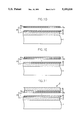
- FlGS. 1A-1F are cross-sectional views depicting successive steps in a process for manufacturing a high dielectric constant capacitor embodying the present invention.
- FIGS. 2-6 are histograms depicting the relationship between deposition speed and deposition time for forming the component layers (Ta 2 O 5 and TiO 2 ) of the high dielectric constant film of respective preferred embodiments of the high dielectric constant capacitor of the present invention.
- FIGS. 1A-1F there can be seen a step-by-step illustration of a process for manufacturing a high dielectric constant capacitor C, in accordance with the present invention.
- the capacitor C embodying the present invention will have particular utility in a semiconductor memory device, such as a DRAM
- the present invention is not limited in its scope to any particular application or environment.
- the present invention is not limited in its scope to a capacitor of any particular type or form.
- the capacitor of the present invention may conveniently be a plane, stacked, hollow-trench, cylindrical, trench, stacked-trench, or pin capacitor.
- the description of the process for manufacturing the capacitor C, in accordance with the present invention, in the process is to form a base film 2 on a silicon substrate 1.
- the base film 2 is preferably made of a conductive material which is selected from a group which includes doped polycrystalline silicon, in-situ doped polycrystalline silicon, amorphous silicon, and tungsten.
- the base film 2 serves as a first electrode of the capacitor C.
- a tantalum oxide film 3 is then deposited on the base film 2, preferably, by means of a low pressure chemical vapor deposition (LPCVD) process.
- the tantalum oxide film 3 is preferably formed to a thickness of between approximately 5 angstroms to approximately 200 angstroms.
- a metal oxide film 4 is then deposited on the tantalum oxide film 3, preferably, also by means of an LPCVD process.
- the metal oxide film 4 is preferably made of a metal oxide whose atomic valence is smaller than that of tantalum and whose dielectric constant is equal to or greater than that of tantalum oxide.
- the metal oxide is selected from a group which includes TiO 2 , SnO 2 , ZrO 2 , HfO 2 , WO 2 , Al 2 O 2 , Cr 2 O 3 , Y 2 O 3 , La 2 O 3 , Bi 2 O 3 , Th 2 O 3 , PbO, BaO, SnO, SrO, CaO, MnO, and MgO.
- TiO 2 , SnO 2 , ZrO 2 , HfO 2 , WO 2 , Al 2 O 2 , Cr 2 O 3 , Y 2 O 3 , La 2 O 3 , Bi 2 O 3 , Th 2 O 3 , PbO, BaO, SnO, SrO, CaO, MnO, and MgO a group which includes TiO 2 , SnO 2 , ZrO 2 , HfO 2 , WO 2 , Al 2 O 2 , Cr 2 O 3 , Y 2 O 3 , La 2 O 3 ,
- the metal oxide film 4 is made of titanium oxide formed to a thickness of less than approximately 50 angstroms, in order to avoid forming a columnar structure. Further, the ratio of the thickness of the tantalum oxide film 3 to the thickness of the metal oxide film 4 is preferably in rne range of 1:10 to 100:1. The tantalum oxide film 3 and the metal oxide film 4 together comprise a first dual-film layer L 1 .
- An additional single layer I may be deposited on the nth dual-film layer L n .
- the additional single layer I may be either a tantalum oxide film or a metal oxide film, such as titanium oxide film.
- the plurality n of dual-film layers, L 1 -L n comprise the high dielectric constant film F of the capacitor C.
- the number n is selected to ensure that the overall thickness of the high dielectric constant film F is sufficient for the particular application for which the capacitor C is utilized, e.g., with respect to dielectric breakdown voltage, capacitance strength, and leakage current.
- the final step in the process for making the capacitor C constitutes forming an upper film 5 on the uppermost layer, either I or 4 n , of the multilayer, high dielectric constant film F.
- the upper film 5 is preferably made of the same conductive material as that of the base film 2.
- the upper film 5 serves as the second electrode of the capacitor C.
- a thermal treatment process may be carried out subsequent to the formation of the upper film 5, in order to relax any residual stress which may be present between any two or more of the multiple layers 3 i , 4 i , of the multilayer, high dielectric constant film F.
- the layers 3 i , 4 i are preferably deposited by a low pressure chemical vapor deposition (LPCVD) process, which is ordinarily carried out under conditions (such as high temperature) sufficient to ensure that the films 3 i , 4 i are deposited evenly and uniformly, it is generally unnecessary to employ this optional thermal treatment process.
- LPCVD low pressure chemical vapor deposition
- MOCVD metallorganic chemical vapor deposition
- FIGS. 2-6 there can be seen histograms which depict the relationship between the deposition speed and deposition time for forming the individual tantalum oxide and titanium oxide (TiO 2 ) films, 3 i , 4 i , of each dual-film layer, L i , of the high dielectric constant film F of respective preferred embodiments of the high dielectric constant capacitor C of the present invention.
- the respective times for deposition of the tantalum oxide film 3 i and the titanium oxide film 4 i of each dual-film layer, L i do not overlap.
- the time at which deposition of each respective titanium oxide film 4 i begins does not overlap the time at which deposition of each respective tantalum oxide film 3 i ends, and vice versa.
- the starting time for the deposition of each respective titanium oxide film 4 i is substantially concurrent with the ending time for the deposition of each respective tantalum oxide film 3 i , and vice versa.
- the respective times for deposition of the tantalum oxide film 3 i and the titanium oxide film 4 i of each dual-film layer, L i partially overlap.
- the deposition of each respective titanium oxide film 4 i begins at a predetermined time before the time at which deposition of each respective tantalum oxide film 3 i ends, and vice versa.
- the starting time for the deposition of each respective titanium oxide film 4 i is separated by a predetermined time interval from the ending time for the deposition of each respective tantalum oxide film 3 i , vice versa.
- the deposition parameters are the same as in the first during the time periods when each respective tantalum oxide film 3 i is being deposited, titanium oxide is simultaneously deposited, but at a very low deposition speed, so that only minute quantities of the titanium oxide are deposited during deposition of each respective tantalum oxide film 3 i .
- the deposition parameters are the same as in the fourth preferred embodiment depicted in FIG. 5, except that, additionally, during the time periods when each respective titanium oxide film 4 i is being deposited, tantalum oxide is simultaneously deposited, but at a very low deposition speed, so that only minute quantities of the tantalum oxide are deposited during deposition of the titanium oxide film 4 i .
- a high dielectric constant capacitor C constructed in accordance with any of the above-described embodiments of the present invention, overcomes the disadvantages of the presently available high dielectric constant capacitors, while simultaneously providing a high dielectric constant capacitor having a dielectric constant which is higher than that of the presently available high dielectric constant capacitors. More particularly, the provision of an ultra-thin metal oxide film 4 over the tantalum oxide film 3 of the dielectric film F, eliminates the prior art problem of unacceptably high leakage current, by avoiding a columnar dielectric film structure, which has been determined to be the principal cause of the aforesaid prior art problem.
- the provision of multiple dual-film layers, L I -L m increases the dielectric constant of the dielectric film F, relative to the prior art, and, also, minimizes the oxygen deficiency of the dielectric film F, thereby substantially increasing the dielectric breakdown voltage of the capacitor C, relative to the prior art.
- the process of the present invention eliminates the lengthy thermal treatment process that is required with the prior art dielectric film deposition process, thereby increasing production speed and improving production efficiency, relative to the prior art.
Abstract
A high dielectric constant film comprised of at least a first dual-film layer, which includes a first tantalum oxide film, and a first metal oxide film which is made of a metal oxide whose valence is smaller than that of tantalum, and whose dielectric constant is equal to or greater than that of tantalum oxide. The first metal oxide film preferably has a thickness of less than approximately 50 angstroms, in order to thereby avoid the formation of a columnar structure, which has been identified as a principal cause of the high leakage current problem which has plagued presently available high dielectric constant capacitors. The first tantalum oxide film preferably has a thickness in the range of between approximately 5 angstroms to approximately 200 angstroms, with the ratio of the thickness of the first tantalum oxide film to the thickness of the first metal oxide film being in the range of 1:10 to 100:1. The high dielectric constant film preferably further includes a plurality of additional dual-film layers formed on the first dual-film layer, to thereby provide a multilayer high dielectric constant film. Each of the additional dual-film layers is preferably of the same construction as that of the first dual-film layer.
The present invention also encompasses a high dielectric constant capacitor which incorporates the above-described high dielectric constant film, and a method for manufacturing the same.
Description
1. Field of the Invention
This invention relates generally to a high dielectric constant capacitor, and, more particularly, to a high dielectric constant capacitor which utilizes a multilayer dielectric film having improved dielectric properties. This invention also relates to a method for making such a high dielectric constant capacitor. It is presently contemplated that this invention may have particular utility in very large scale integrated circuits (VLSIs), such as semiconductor memory devices, e.g. RAMs.
2. Description of the Prior Art
VLSIs, such as semiconductor memory devices having a large memory capacity, utilize miniature capacitors which are required to have a high capacitance, despite their small area. In order to achieve the required high capacitance, dielectric films having a high dielectric constant, such as tantalum oxide (Ta2 O5) films, have been used in such miniature capacitors.
Generally, such tantalum oxide dielectric films are formed by means of a low pressure chemical vapor deposition (LPCVD) technique. However, tantalum oxide dielectric films formed in such a manner exhibit oxygen deficiency, which results in capacitor performance problems, such as unacceptably high leakage current and unacceptably low dielectric breakdown voltage.
One approach which has been proposed to overcome the above-mentioned drawbacks with tantalum oxide dielectric films, is described in U.S. Pat. No. 4,734,340, issued to Saito et al., and, in an article entitled "Electrical Properties of Thin Ta2 O5 Films Grown By Chemical Vapor Deposition", @ pp. 680-683 of the IEDM Technical Digest (1986), by Saito et al. In accordance with this approach, the dielectric film is made of a mixture of tantalum oxide and titanium oxide. However, this approach only partially solves the oxygen deficiency problem, because the ratio of Ti to Ta is limited to a range of from 0.1 to 4 atomic
Thus, there still exists a need for a high dielectric constant capacitor which more fully overcomes the above-described drawbacks of presently available high dielectric constant capacitors. The present invention fulfills this need, while also providing a miniature capacitor which has a higher dielectric constant than the presently available miniature capacitors.
The present invention encompasses a high dielectric constant film comprised of at least a first dual-film layer, which includes a first tantalum oxide film, and a first metal oxide film which is made of a metal oxide whose valence is smaller than that of tantalum, and whose dielectric constant is equal to or greater than that of tantalum oxide. The first metal oxide film preferably has a thickness of less than approximately 50 angstroms, in order to thereby avoid the formation of a columnar structure which has been identified as a principal cause of the high leakage current problem which has plagued presently available high dielectric constant capacitors. The first tantalum oxide film preferably has a thickness in the range of between approximately 5 angstroms to approximately 200 angstroms, with the ratio of the thickness of the first tantalum oxide film to the thickness of the first metal oxide film being in the range of 1:10 to 100:1. The high dielectric constant film preferably further includes a plurality of additional dual-film layers formed on the first dual-film layer, to thereby provide a multilayer high dielectric constant film. Each of the additional dual-film layers is preferably of the same construction as that of the first dual-film layer. Optionally, an additional single layer of tantalum oxide or metal oxide may be formed on an uppermost one of the dual-film layers.
The present invention also encompasses a high above-described high dielectric constant film, and a method for manufacturing the same.
These and various other features and advantages of the present invention will be readily understood with reference to the following detailed description taken in conjunction with the accompanying drawings, wherein like reference numerals designate like structural elements, and, in which:
FlGS. 1A-1F are cross-sectional views depicting successive steps in a process for manufacturing a high dielectric constant capacitor embodying the present invention; and,
FIGS. 2-6 are histograms depicting the relationship between deposition speed and deposition time for forming the component layers (Ta2 O5 and TiO2) of the high dielectric constant film of respective preferred embodiments of the high dielectric constant capacitor of the present invention.
With reference now to FIGS. 1A-1F, there can be seen a step-by-step illustration of a process for manufacturing a high dielectric constant capacitor C, in accordance with the present invention. Although it is presently contemplated that the capacitor C embodying the present invention will have particular utility in a semiconductor memory device, such as a DRAM, it should be immediately recognized that the present invention is not limited in its scope to any particular application or environment. Further, it should also be immediately recognized that the present invention is not limited in its scope to a capacitor of any particular type or form. For example, the capacitor of the present invention may conveniently be a plane, stacked, hollow-trench, cylindrical, trench, stacked-trench, or pin capacitor.
Referring specifically now to FIG. 1A, the description of the process for manufacturing the capacitor C, in accordance with the present invention, in the process is to form a base film 2 on a silicon substrate 1. The base film 2 is preferably made of a conductive material which is selected from a group which includes doped polycrystalline silicon, in-situ doped polycrystalline silicon, amorphous silicon, and tungsten. The base film 2 serves as a first electrode of the capacitor C.
With reference to FIG. 1B, a tantalum oxide film 3 is then deposited on the base film 2, preferably, by means of a low pressure chemical vapor deposition (LPCVD) process. The tantalum oxide film 3 is preferably formed to a thickness of between approximately 5 angstroms to approximately 200 angstroms.
With reference to FIG. 1C, a metal oxide film 4 is then deposited on the tantalum oxide film 3, preferably, also by means of an LPCVD process. The metal oxide film 4 is preferably made of a metal oxide whose atomic valence is smaller than that of tantalum and whose dielectric constant is equal to or greater than that of tantalum oxide. Most preferably, the metal oxide is selected from a group which includes TiO2, SnO2, ZrO2, HfO2, WO2, Al2 O2, Cr2 O3, Y2 O3, La2 O3, Bi2 O3, Th2 O3, PbO, BaO, SnO, SrO, CaO, MnO, and MgO. However, it should be clearly understood that this list of metal oxides is intended to be illustrative, and not exhaustive, and thus, is not limiting to the present invention. In the presently contemplated best mode of the present invention, the metal oxide film 4 is made of titanium oxide formed to a thickness of less than approximately 50 angstroms, in order to avoid forming a columnar structure. Further, the ratio of the thickness of the tantalum oxide film 3 to the thickness of the metal oxide film 4 is preferably in rne range of 1:10 to 100:1. The tantalum oxide film 3 and the metal oxide film 4 together comprise a first dual-film layer L1.
Preferably, as can be seen in FIGS. 1D and 1E, the steps of depositing the tantalum oxide film 3 and the metal oxide film 4 are sequentially repeated, a selected number of times, to thereby form a plurality of dual-film layers, L1 -Ln, each of which is comprised of a respective tantalum oxide film 3i and a respective metal oxide film 4i, where i=1 through n, and n is a positive integer equal to or greater than 2. An additional single layer I may be deposited on the nth dual-film layer Ln. The additional single layer I may be either a tantalum oxide film or a metal oxide film, such as titanium oxide film.
Collectively, the plurality n of dual-film layers, L1 -Ln, comprise the high dielectric constant film F of the capacitor C. The number n is selected to ensure that the overall thickness of the high dielectric constant film F is sufficient for the particular application for which the capacitor C is utilized, e.g., with respect to dielectric breakdown voltage, capacitance strength, and leakage current.
With reference to FIG. 1F, the final step in the process for making the capacitor C constitutes forming an upper film 5 on the uppermost layer, either I or 4n, of the multilayer, high dielectric constant film F. the upper film 5 is preferably made of the same conductive material as that of the base film 2. The upper film 5 serves as the second electrode of the capacitor C.
Optionally, a thermal treatment process may be carried out subsequent to the formation of the upper film 5, in order to relax any residual stress which may be present between any two or more of the multiple layers 3i, 4i, of the multilayer, high dielectric constant film F. However, since the layers 3i, 4i are preferably deposited by a low pressure chemical vapor deposition (LPCVD) process, which is ordinarily carried out under conditions (such as high temperature) sufficient to ensure that the films 3i, 4i are deposited evenly and uniformly, it is generally unnecessary to employ this optional thermal treatment process.
Although not limiting to the practice of the present invention, the above-described process of the present invention can be conveniently carried out with a metallorganic chemical vapor deposition (MOCVD) apparatus (not shown) connected to a suitable metallorganic supply (not shown).
With reference now to FIGS. 2-6, there can be seen histograms which depict the relationship between the deposition speed and deposition time for forming the individual tantalum oxide and titanium oxide (TiO2) films, 3i, 4i, of each dual-film layer, Li, of the high dielectric constant film F of respective preferred embodiments of the high dielectric constant capacitor C of the present invention.
With particular reference now to FIG. 2, in a first preferred embodiment of the process of the present invention, the respective times for deposition of the tantalum oxide film 3i and the titanium oxide film 4i of each dual-film layer, Li, do not overlap. In other words, the time at which deposition of each respective titanium oxide film 4i begins does not overlap the time at which deposition of each respective tantalum oxide film 3i ends, and vice versa. Rather, in accordance with this first preferred embodiment, the starting time for the deposition of each respective titanium oxide film 4i is substantially concurrent with the ending time for the deposition of each respective tantalum oxide film 3i, and vice versa.
With reference to FIG. 3, in a second preferred embodiment of the process of the present invention, the respective times for deposition of the tantalum oxide film 3i and the titanium oxide film 4i of each dual-film layer, Li, partially overlap. In other words, the deposition of each respective titanium oxide film 4i begins at a predetermined time before the time at which deposition of each respective tantalum oxide film 3i ends, and vice versa.
With reference to FIG. 4, in a third preferred embodiment of the process of the present invention, the starting time for the deposition of each respective titanium oxide film 4i is separated by a predetermined time interval from the ending time for the deposition of each respective tantalum oxide film 3i, vice versa.
With reference to FIG. 5, in a fourth preferred embodiment of the process of the present invention, the deposition parameters are the same as in the first during the time periods when each respective tantalum oxide film 3i is being deposited, titanium oxide is simultaneously deposited, but at a very low deposition speed, so that only minute quantities of the titanium oxide are deposited during deposition of each respective tantalum oxide film 3i.
With reference to FIG. 6, in a fifth preferred embodiment of the process of the present invention, the deposition parameters are the same as in the fourth preferred embodiment depicted in FIG. 5, except that, additionally, during the time periods when each respective titanium oxide film 4i is being deposited, tantalum oxide is simultaneously deposited, but at a very low deposition speed, so that only minute quantities of the tantalum oxide are deposited during deposition of the titanium oxide film 4i.
As will be appreciated by those skilled in the art, a high dielectric constant capacitor C constructed in accordance with any of the above-described embodiments of the present invention, overcomes the disadvantages of the presently available high dielectric constant capacitors, while simultaneously providing a high dielectric constant capacitor having a dielectric constant which is higher than that of the presently available high dielectric constant capacitors. More particularly, the provision of an ultra-thin metal oxide film 4 over the tantalum oxide film 3 of the dielectric film F, eliminates the prior art problem of unacceptably high leakage current, by avoiding a columnar dielectric film structure, which has been determined to be the principal cause of the aforesaid prior art problem. Further, the provision of multiple dual-film layers, LI -Lm, increases the dielectric constant of the dielectric film F, relative to the prior art, and, also, minimizes the oxygen deficiency of the dielectric film F, thereby substantially increasing the dielectric breakdown voltage of the capacitor C, relative to the prior art. Moreover, the process of the present invention eliminates the lengthy thermal treatment process that is required with the prior art dielectric film deposition process, thereby increasing production speed and improving production efficiency, relative to the prior art.
Although several preferred embodiments of the present invention have been described in detail hereinabove, it should be clearly understood that many variations and/or modifications of the basic inventive concepts herein taught which may appear to those skilled in the pertinent art will still fall within the spirit and scope of the present invention, as defined in the appended claims.
Claims (30)
1. A high dielectric constant capacitor, including:
a substrate;
a first electrode film formed on said substrate;
a first tantalum oxide film formed on said first electrode film;
a first metal oxide film formed on said first tantalum oxide film, wherein said first metal oxide film is made of a metal oxide whose valence is smaller than that of tantalum, and whose dielectric constant is equal to or greater than that of tantalum oxide;
wherein said first tantalum oxide film and said first metal oxide film together comprise a high dielectric constant film; and
a second electrode film formed on said high dielectric constant film.
2. The capacitor as set forth in claim 1, wherein said first tantalum oxide film has a thickness in the range of between approximately 5 angstroms to approximately 200 angstroms.
3. The capacitor as set forth in claim 1, wherein said first metal oxide film has a thickness of less than approximately 50 angstroms.
4. The capacitor as set forth in claim 3, wherein the ratio of the thickness of said first tantalum oxide film to the thickness of said first metal oxide film is in the range of 1:10 to 100:1.
5. The capacitor as set forth in claim 4, wherein said metal oxide is selected from a group comprised of TiO2, SnO2, ZrO2, HfO2, WO2, Al2 O3, Cr2 O3, Y2 O3, La2 O3, Bi2 O3, Th2 O3, PbO, BaO, SnO, SrO, CaO, MnO, and MgO.
6. The capacitor as set forth in claim 1, wherein said high dielectric constant film further includes a plurality of additional dual-film layers formed on said first dual-film layer, wherein each of said additional dual-film layers is comprised of a respective tantalum oxide film and a respective metal oxide film.
7. The capacitor as set forth in claim 6, wherein said high dielectric constant film further includes an additional single layer of tantalum oxide formed on an uppermost one of said additional dual-film layers.
8. The capacitor as set forth in claim 6, wherein said high dielectric constant film further includes an additional single layer of metal oxide formed on an uppermost one of said additional dual-film layers.
9. The capacitor as set forth in claim 6, wherein said respective metal oxide film of each said additional dual-film layer is also made of said metal oxide.
10. The capacitor as set forth in claim 9, wherein said metal oxide is selected from a group comprised of TiO2, SnO2, ZrO2, HfO2, WO2, Al2 O3, Cr2 O3, Y2 O3, La2 O3, Bi2 O3, Th2 O3, PbO, BaO, SnO, SrO, CaO, MnO, and MgO.
11. The capacitor as set forth in claim 10, wherein the ratio of the thickness of said respective tantalum oxide film of each said additional dual-film layer to the thickness of said respective metal oxide film of each said 1:10 to 100:1.
12. The capacitor as set forth in claim 11, wherein said respective tantalum oxide layer of each said additional dual-film layer has a thickness in the range of between approximately 5 angstroms to approximately 200 angstroms.
13. The capacitor as set forth in claim 12, wherein said respective metal oxide layer of each said additional dual-film layer has a thickness of less than approximately 50 angstroms.
14. A method for manufacturing a high dielectric constant capacitor, including the steps of:
forming a first electrode film on a substrate;
forming a first tantalum oxide film on said first electrode film;
forming a first metal oxide film on said first tantalum oxide film, said metal oxide film being formed of a metal oxide whose valence is smaller than that of tantalum, and whose dielectric constant is equal to or greater than that of tantalum oxide, whereby said first tantalum oxide film and said first metal oxide film together comprise a high dielectric constant film; and,
forming a second electrode film on said high dielectric constant film.
15. The method as set forth in claim 14, further including the steps of:
forming an additional tantalum oxide film on said first metal oxide film; and,
forming an additional metal oxide film on said additional tantalum oxide film.
16. The method as set forth in claim 14, further including the step of sequentially repeating said forming a tantalum oxide step and said forming a metal oxide film step, a plurality of times, to thereby form a plurality, n, of dual-film layers, each comprised of a respective tantalum oxide film and a respective metal oxide film;
wherein said first tantalum oxide film and said first metal oxide film together comprise a first one of said n dual-film layers, and the last-formed tantalum oxide film and the last-formed metal oxide film together comprise an nth one of said n dual-film layers; and,
wherein further, said n dual-film layers together comprise said high dielectric constant film.
17. The method as set forth in claim 16, wherein said tantalum oxide film of each of said n dual-film layers is formed to a thickness in the range of between approximately 5 angstroms to approximately 200 angstroms.
18. The method as set forth in claim 17, wherein said metal oxide film of each of said n dual-film layers is formed to a thickness of less than approximately 50 angstroms.
19. The method as set forth in claim 18, wherein the ratio of the thickness of said tantalum oxide film of each of said n dual-film layers to the thickness of said metal oxide film of each of said n dual-film layers, is in the range of 1:10 to 100:1.
20. The method as set forth in claim 19, wherein said metal oxide is selected from a group comprised of TiO2, SnO2, ZrO2, HfO2, WO2, Al2 O3, Cr2 O3, Y2 O3, La2 O3, Bi2 O3, Th2 O3, PbO, BaO, SnO, SrO, CaO, MnO, and MgO.
21. The method as set forth in claim 20, further including the step of forming an additional said n dual-film layers.
22. The method as set forth in claim 20, further including the step of forming an additional single layer of said metal oxide on said nth one of said n dual-film layers.
23. The method as set forth in claim 19, wherein said step of forming a first tantalum oxide film, said step of forming a first metal oxide film, and said sequentially repeating step, are each vapor deposition process.
24. The method as set forth in claim 19, wherein said step of forming a first tantalum oxide film, said step of forming a first metal oxide film, and said sequentially repeating step, are carried out by means of a deposition process whereby the time at which deposition of said metal oxide film of each of said n dual-film layers begins, does not overlap the time at which deposition of its corresponding said tantalum oxide film ends, and vice versa.
25. The method as set forth in claim 24, wherein the starting time for deposition of said metal oxide film of each of said n dual-film layers, is substantially concurrent with the ending time for the deposition of its corresponding said tantalum oxide film, and vice versa.
26. The method as set forth in claim 24, wherein the starting time for deposition of said metal oxide film of each of said n dual-film layers, is separated by a predetermined time interval from the ending time for the deposition of its corresponding said tantalum oxide film, and vice versa.
27. The method as set forth in claim 19, wherein said step of forming a first tantalum oxide film, said step of forming a first metal oxide film, and said sequentially repeating step, are carried out by means of a deposition process whereby the time at which deposition of said metal oxide film of each of said n dual-film layers begins, partially overlaps the time at which deposition of its corresponding said tantalum oxide film ends, and vice versa.
28. The method as set forth in claim 19, where said step of forming a first tantalum oxide film, said step of forming a first metal oxide film, and said sequentially repeating step, are carried during deposition of said tantalum oxide film of each of said n dual-film layers, said metal oxide is simultaneously deposited, but at a very low deposition speed, so that only minute quantities of said metal oxide are deposited during deposition of said tantalum oxide film of each of said n dual-film layers.
29. The method as set forth in claim 28, wherein, additionally, during deposition of said metal oxide film of each of said n dual-film layers, said tantalum oxide is simultaneously deposited, but at a very low deposition speed, so that only minute quantities of said tantalum oxide are deposited during deposition of said metal oxide film of each of said n dual-film layers.
30. The method as set forth in claim 19, wherein said first electrode film and said second electrode film are made of a conductive material selected from a group comprised of doped polycrystalline silicon, amorphous silicon, and tungsten.
Applications Claiming Priority (2)
| Application Number | Priority Date | Filing Date | Title |
|---|---|---|---|
| KR1019910011272A KR930012120B1 (en) | 1991-07-03 | 1991-07-03 | Semicondcutor device and fabricating method thereof |
| KR91-11272 | 1991-07-03 |
Publications (1)
| Publication Number | Publication Date |
|---|---|
| US5195018A true US5195018A (en) | 1993-03-16 |
Family
ID=19316723
Family Applications (1)
| Application Number | Title | Priority Date | Filing Date |
|---|---|---|---|
| US07/899,973 Expired - Lifetime US5195018A (en) | 1991-07-03 | 1992-06-17 | High dielectric constant capacitor and method for manufacturing the same |
Country Status (5)
| Country | Link |
|---|---|
| US (1) | US5195018A (en) |
| KR (1) | KR930012120B1 (en) |
| DE (1) | DE4221959A1 (en) |
| FR (1) | FR2678766A1 (en) |
| GB (1) | GB2257829A (en) |
Cited By (54)
| Publication number | Priority date | Publication date | Assignee | Title |
|---|---|---|---|---|
| US5383088A (en) * | 1993-08-09 | 1995-01-17 | International Business Machines Corporation | Storage capacitor with a conducting oxide electrode for metal-oxide dielectrics |
| US5474949A (en) * | 1992-01-27 | 1995-12-12 | Matsushita Electric Industrial Co., Ltd. | Method of fabricating capacitor or contact for semiconductor device by forming uneven oxide film and reacting silicon with metal containing gas |
| US5573979A (en) * | 1995-02-13 | 1996-11-12 | Texas Instruments Incorporated | Sloped storage node for a 3-D dram cell structure |
| US5590017A (en) * | 1995-04-03 | 1996-12-31 | Aluminum Company Of America | Alumina multilayer wiring substrate provided with high dielectric material layer |
| US5872696A (en) * | 1997-04-09 | 1999-02-16 | Fujitsu Limited | Sputtered and anodized capacitors capable of withstanding exposure to high temperatures |
| EP1020896A1 (en) * | 1999-01-13 | 2000-07-19 | Lucent Technologies Inc. | Integrated circuit device with composite oxide dielectric |
| WO2000070674A1 (en) * | 1999-05-12 | 2000-11-23 | Infineon Technologies Ag | Capacitor for a semiconductor arrangement and method for producing a dielectric layer for the capacitor |
| US6235594B1 (en) | 1999-01-13 | 2001-05-22 | Agere Systems Guardian Corp. | Methods of fabricating an integrated circuit device with composite oxide dielectric |
| WO2001054200A1 (en) * | 2000-01-19 | 2001-07-26 | North Carolina State University | Lanthanum oxide-based gate dielectrics for integrated circuit field effect transistors and methods of fabricating same |
| DE10010821A1 (en) * | 2000-02-29 | 2001-09-13 | Infineon Technologies Ag | Increasing capacity in a storage trench comprises depositing a first silicon oxide layer in the trench, depositing a silicon layer over the first layer to sufficiently |
| US6341056B1 (en) * | 2000-05-17 | 2002-01-22 | Lsi Logic Corporation | Capacitor with multiple-component dielectric and method of fabricating same |
| US6342734B1 (en) | 2000-04-27 | 2002-01-29 | Lsi Logic Corporation | Interconnect-integrated metal-insulator-metal capacitor and method of fabricating same |
| US20020074584A1 (en) * | 2000-12-20 | 2002-06-20 | Micron Technology, Inc. | Low leakage MIM capacitor |
| US6417535B1 (en) | 1998-12-23 | 2002-07-09 | Lsi Logic Corporation | Vertical interdigitated metal-insulator-metal capacitor for an integrated circuit |
| US6432793B1 (en) | 1997-12-12 | 2002-08-13 | Micron Technology, Inc. | Oxidative conditioning method for metal oxide layer and applications thereof |
| US6441419B1 (en) | 1998-03-31 | 2002-08-27 | Lsi Logic Corporation | Encapsulated-metal vertical-interdigitated capacitor and damascene method of manufacturing same |
| US20020125998A1 (en) * | 1998-06-22 | 2002-09-12 | Petite Thomas D. | System and method for monitoring and controlling remote devices |
| US20020167038A1 (en) * | 2000-08-30 | 2002-11-14 | Jiong-Ping Lu | Novel high-k dielectric materials and processes for manufacturing them |
| US6504202B1 (en) | 2000-02-02 | 2003-01-07 | Lsi Logic Corporation | Interconnect-embedded metal-insulator-metal capacitor |
| US6566186B1 (en) | 2000-05-17 | 2003-05-20 | Lsi Logic Corporation | Capacitor with stoichiometrically adjusted dielectric and method of fabricating same |
| US6627503B2 (en) * | 2000-02-11 | 2003-09-30 | Sharp Laboratories Of America, Inc. | Method of forming a multilayer dielectric stack |
| US6627939B2 (en) * | 1999-12-09 | 2003-09-30 | Nec Corporation | Semiconductor device provided with a capacitor having a high-permittivity insulator film |
| US20040043630A1 (en) * | 2002-08-28 | 2004-03-04 | Micron Technology, Inc. | Systems and methods for forming metal oxides using metal organo-amines and metal organo-oxides |
| US20040040501A1 (en) * | 2002-08-28 | 2004-03-04 | Micron Technology, Inc. | Systems and methods for forming zirconium and/or hafnium-containing layers |
| US20040043632A1 (en) * | 2002-08-28 | 2004-03-04 | Micron Technology, Inc. | Systems and methods for forming metal oxides using alcohols |
| WO2004086486A1 (en) | 2003-03-26 | 2004-10-07 | Riken | Process for producing dielectric insulating thin film, and dielectric insulating material |
| US20050043059A1 (en) * | 2000-08-09 | 2005-02-24 | Petite Thomas D. | Systems and methods for providing remote monitoring of electricity consumption for an electric meter |
| US20050059206A1 (en) * | 2003-03-19 | 2005-03-17 | Jung-Hee Chung | Integrated circuit devices having barrier layers between upper electrodes and dielectric layers and methods of fabricating the same |
| US20050195775A1 (en) * | 2004-03-03 | 2005-09-08 | Petite Thomas D. | System and method for monitoring remote devices with a dual-mode wireless communication protocol |
| US20060145294A1 (en) * | 2003-08-06 | 2006-07-06 | Vishwanath Bhat | Methods of forming capacitors |
| US20060151845A1 (en) * | 2005-01-07 | 2006-07-13 | Shrinivas Govindarajan | Method to control interfacial properties for capacitors using a metal flash layer |
| US20060151823A1 (en) * | 2005-01-07 | 2006-07-13 | Shrinivas Govindarajan | High dielectric constant materials |
| US7079810B2 (en) | 1997-02-14 | 2006-07-18 | Statsignal Ipc, Llc | System and method for communicating with a remote communication unit via the public switched telephone network (PSTN) |
| US7103511B2 (en) | 1998-10-14 | 2006-09-05 | Statsignal Ipc, Llc | Wireless communication networks for providing remote monitoring of devices |
| US20060205143A1 (en) * | 2005-01-07 | 2006-09-14 | Shrinivas Govindarajan | DRAM with high K dielectric storage capacitor and method of making the same |
| US7137550B1 (en) | 1997-02-14 | 2006-11-21 | Statsignal Ipc, Llc | Transmitter for accessing automated financial transaction machines |
| US20070012973A1 (en) * | 2005-06-30 | 2007-01-18 | Kabushiki Kaisha Toshiba | Semiconductor device having MIM capacitor and manufacturing method thereof |
| US7263073B2 (en) | 1999-03-18 | 2007-08-28 | Statsignal Ipc, Llc | Systems and methods for enabling a mobile user to notify an automated monitoring system of an emergency situation |
| US7295128B2 (en) | 1998-06-22 | 2007-11-13 | Sipco, Llc | Smoke detection methods, devices, and systems |
| US20080106846A1 (en) * | 2002-05-15 | 2008-05-08 | Raytheon Company | Electrode for thin film capacitor devices |
| US7650425B2 (en) | 1999-03-18 | 2010-01-19 | Sipco, Llc | System and method for controlling communication between a host computer and communication devices associated with remote devices in an automated monitoring system |
| US7697492B2 (en) | 1998-06-22 | 2010-04-13 | Sipco, Llc | Systems and methods for monitoring and controlling remote devices |
| US7756086B2 (en) | 2004-03-03 | 2010-07-13 | Sipco, Llc | Method for communicating in dual-modes |
| US8000314B2 (en) | 1996-12-06 | 2011-08-16 | Ipco, Llc | Wireless network system and method for providing same |
| US8064412B2 (en) | 1998-06-22 | 2011-11-22 | Sipco, Llc | Systems and methods for monitoring conditions |
| US8171136B2 (en) | 2001-10-30 | 2012-05-01 | Sipco, Llc | System and method for transmitting pollution information over an integrated wireless network |
| US8410931B2 (en) | 1998-06-22 | 2013-04-02 | Sipco, Llc | Mobile inventory unit monitoring systems and methods |
| US8489063B2 (en) | 2001-10-24 | 2013-07-16 | Sipco, Llc | Systems and methods for providing emergency messages to a mobile device |
| US8666357B2 (en) | 2001-10-24 | 2014-03-04 | Sipco, Llc | System and method for transmitting an emergency message over an integrated wireless network |
| US8787246B2 (en) | 2009-02-03 | 2014-07-22 | Ipco, Llc | Systems and methods for facilitating wireless network communication, satellite-based wireless network systems, and aircraft-based wireless network systems, and related methods |
| DE102014003603A1 (en) | 2014-03-17 | 2015-09-17 | Treofan Germany Gmbh & Co. Kg | Electrical insulating foil for use in capacitors |
| US9439126B2 (en) | 2005-01-25 | 2016-09-06 | Sipco, Llc | Wireless network protocol system and methods |
| CN110415974A (en) * | 2019-07-17 | 2019-11-05 | 南京大学 | One kind is based on nano-stack structured metal oxide flexible capacitor and preparation method thereof |
| US11276531B2 (en) | 2017-05-31 | 2022-03-15 | Tdk Corporation | Thin-film capacitor and method for manufacturing thin-film capacitor |
Families Citing this family (13)
| Publication number | Priority date | Publication date | Assignee | Title |
|---|---|---|---|---|
| DE4300808C1 (en) * | 1993-01-14 | 1994-03-17 | Siemens Ag | Film capacitor prodn. from 2 types of conductive films and dielectric - using selective under-etching of one type of conductive film in each contact hole to increase capacity e.g. for passive device or IC |
| US5471364A (en) * | 1993-03-31 | 1995-11-28 | Texas Instruments Incorporated | Electrode interface for high-dielectric-constant materials |
| KR100549566B1 (en) * | 1998-10-29 | 2007-12-21 | 주식회사 하이닉스반도체 | Capacitor Formation Method of Semiconductor Device |
| JP3189813B2 (en) * | 1998-11-30 | 2001-07-16 | 日本電気株式会社 | Method for manufacturing semiconductor device |
| KR100705926B1 (en) * | 1999-12-22 | 2007-04-11 | 주식회사 하이닉스반도체 | Method of manufacturing a capacitor in a semiconductor device |
| KR100624903B1 (en) * | 1999-12-22 | 2006-09-19 | 주식회사 하이닉스반도체 | Method of manufacturing a capacitor in a semiconductor device |
| KR100551884B1 (en) * | 1999-12-29 | 2006-02-10 | 주식회사 하이닉스반도체 | Method of manufacturing a capacitor in a semiconductor device |
| KR100367404B1 (en) * | 1999-12-31 | 2003-01-10 | 주식회사 하이닉스반도체 | Method of forming capacitor with multi-layered TaON dielectic layer |
| KR100451037B1 (en) * | 2000-12-08 | 2004-10-02 | 주식회사 하이닉스반도체 | Method of forming a gate electrode in a semiconductor device |
| KR100464650B1 (en) * | 2002-04-23 | 2005-01-03 | 주식회사 하이닉스반도체 | Capacitor of semiconductor device having dual dielectric layer structure and method for fabricating the same |
| KR100431306B1 (en) * | 2002-08-30 | 2004-05-12 | 주식회사 하이닉스반도체 | Method for formig gate of semiconductor device using gate oxide made of double film of aluminium oxide and yttrium oxynitride |
| KR100494124B1 (en) * | 2002-12-09 | 2005-06-13 | 주식회사 하이닉스반도체 | Method for forming MIM structure capacitor |
| KR100596805B1 (en) * | 2005-06-30 | 2006-07-04 | 주식회사 하이닉스반도체 | Method for forming capacitor of semiconductor device |
Citations (4)
| Publication number | Priority date | Publication date | Assignee | Title |
|---|---|---|---|---|
| US4437139A (en) * | 1982-12-17 | 1984-03-13 | International Business Machines Corporation | Laser annealed dielectric for dual dielectric capacitor |
| US4734340A (en) * | 1985-07-16 | 1988-03-29 | Sony Corporation | Dielectric thin film |
| US4959745A (en) * | 1988-03-04 | 1990-09-25 | Kabushiki Kaisha Toshiba | Capacitor and method for producing the same |
| US5111355A (en) * | 1990-09-13 | 1992-05-05 | National Semiconductor Corp. | High value tantalum oxide capacitor |
Family Cites Families (5)
| Publication number | Priority date | Publication date | Assignee | Title |
|---|---|---|---|---|
| US4062749A (en) * | 1976-02-09 | 1977-12-13 | Corning Glass Works | Method of forming a thin film capacitor with a manganese dioxide layer |
| JPS5745968A (en) * | 1980-08-29 | 1982-03-16 | Ibm | Capacitor with double dielectric unit |
| JP2617457B2 (en) * | 1985-11-29 | 1997-06-04 | 株式会社日立製作所 | Semiconductor device and manufacturing method thereof |
| JPS62222512A (en) * | 1986-03-20 | 1987-09-30 | キヤノン株式会社 | Dielectric material |
| KR920006736B1 (en) * | 1989-11-08 | 1992-08-17 | 삼성전자 주식회사 | Semiconductor device and method for manufacturing thereof |
-
1991
- 1991-07-03 KR KR1019910011272A patent/KR930012120B1/en active IP Right Grant
-
1992
- 1992-06-17 US US07/899,973 patent/US5195018A/en not_active Expired - Lifetime
- 1992-06-19 GB GB9213070A patent/GB2257829A/en not_active Withdrawn
- 1992-07-02 DE DE4221959A patent/DE4221959A1/en not_active Withdrawn
- 1992-07-03 FR FR9208264A patent/FR2678766A1/en active Pending
Patent Citations (4)
| Publication number | Priority date | Publication date | Assignee | Title |
|---|---|---|---|---|
| US4437139A (en) * | 1982-12-17 | 1984-03-13 | International Business Machines Corporation | Laser annealed dielectric for dual dielectric capacitor |
| US4734340A (en) * | 1985-07-16 | 1988-03-29 | Sony Corporation | Dielectric thin film |
| US4959745A (en) * | 1988-03-04 | 1990-09-25 | Kabushiki Kaisha Toshiba | Capacitor and method for producing the same |
| US5111355A (en) * | 1990-09-13 | 1992-05-05 | National Semiconductor Corp. | High value tantalum oxide capacitor |
Non-Patent Citations (2)
| Title |
|---|
| M. Saitoh, T. Mori and H. Tamura; "Electrical Properties of THIN Ta2 O5 Films Grown by Chemical Vapor Deposition"; 1986 IEEE, pp. 680-683, CH. 2381. |
| M. Saitoh, T. Mori and H. Tamura; Electrical Properties of THIN Ta 2 O 5 Films Grown by Chemical Vapor Deposition ; 1986 IEEE, pp. 680 683, CH. 2381. * |
Cited By (123)
| Publication number | Priority date | Publication date | Assignee | Title |
|---|---|---|---|---|
| US5661068A (en) * | 1992-01-27 | 1997-08-26 | Matsushita Electric Industrial Co., Ltd. | Method of fabricating a semiconductor device |
| US5474949A (en) * | 1992-01-27 | 1995-12-12 | Matsushita Electric Industrial Co., Ltd. | Method of fabricating capacitor or contact for semiconductor device by forming uneven oxide film and reacting silicon with metal containing gas |
| US5693557A (en) * | 1992-01-27 | 1997-12-02 | Matsushita Electric Industrial Co., Ltd. | Method of fabricating a semiconductor device |
| US5383088A (en) * | 1993-08-09 | 1995-01-17 | International Business Machines Corporation | Storage capacitor with a conducting oxide electrode for metal-oxide dielectrics |
| US5573979A (en) * | 1995-02-13 | 1996-11-12 | Texas Instruments Incorporated | Sloped storage node for a 3-D dram cell structure |
| US5590017A (en) * | 1995-04-03 | 1996-12-31 | Aluminum Company Of America | Alumina multilayer wiring substrate provided with high dielectric material layer |
| US8233471B2 (en) | 1996-12-06 | 2012-07-31 | Ipco, Llc | Wireless network system and method for providing same |
| US8000314B2 (en) | 1996-12-06 | 2011-08-16 | Ipco, Llc | Wireless network system and method for providing same |
| US8982856B2 (en) | 1996-12-06 | 2015-03-17 | Ipco, Llc | Systems and methods for facilitating wireless network communication, satellite-based wireless network systems, and aircraft-based wireless network systems, and related methods |
| US8625496B2 (en) | 1996-12-06 | 2014-01-07 | Ipco, Llc | Wireless network system and method for providing same |
| US7079810B2 (en) | 1997-02-14 | 2006-07-18 | Statsignal Ipc, Llc | System and method for communicating with a remote communication unit via the public switched telephone network (PSTN) |
| US7137550B1 (en) | 1997-02-14 | 2006-11-21 | Statsignal Ipc, Llc | Transmitter for accessing automated financial transaction machines |
| US5872696A (en) * | 1997-04-09 | 1999-02-16 | Fujitsu Limited | Sputtered and anodized capacitors capable of withstanding exposure to high temperatures |
| US20040166672A1 (en) * | 1997-12-12 | 2004-08-26 | Reinberg Alan R. | Oxidative conditioning compositions for metal oxide layer and applications thereof |
| US6887579B2 (en) | 1997-12-12 | 2005-05-03 | Micron Technology, Inc. | Oxidative conditioning compositions for metal oxide layer and applications thereof |
| US6896969B2 (en) | 1997-12-12 | 2005-05-24 | Micron Technology, Inc. | Oxidative conditioning compositions for metal oxide layer and applications thereof |
| US6432793B1 (en) | 1997-12-12 | 2002-08-13 | Micron Technology, Inc. | Oxidative conditioning method for metal oxide layer and applications thereof |
| US6441419B1 (en) | 1998-03-31 | 2002-08-27 | Lsi Logic Corporation | Encapsulated-metal vertical-interdigitated capacitor and damascene method of manufacturing same |
| US9691263B2 (en) | 1998-06-22 | 2017-06-27 | Sipco, Llc | Systems and methods for monitoring conditions |
| US7697492B2 (en) | 1998-06-22 | 2010-04-13 | Sipco, Llc | Systems and methods for monitoring and controlling remote devices |
| US8410931B2 (en) | 1998-06-22 | 2013-04-02 | Sipco, Llc | Mobile inventory unit monitoring systems and methods |
| US9571582B2 (en) | 1998-06-22 | 2017-02-14 | Sipco, Llc | Systems and methods for monitoring and controlling remote devices |
| US8223010B2 (en) | 1998-06-22 | 2012-07-17 | Sipco Llc | Systems and methods for monitoring vehicle parking |
| US8212667B2 (en) | 1998-06-22 | 2012-07-03 | Sipco, Llc | Automotive diagnostic data monitoring systems and methods |
| US8064412B2 (en) | 1998-06-22 | 2011-11-22 | Sipco, Llc | Systems and methods for monitoring conditions |
| US8013732B2 (en) | 1998-06-22 | 2011-09-06 | Sipco, Llc | Systems and methods for monitoring and controlling remote devices |
| US8964708B2 (en) | 1998-06-22 | 2015-02-24 | Sipco Llc | Systems and methods for monitoring and controlling remote devices |
| US20020125998A1 (en) * | 1998-06-22 | 2002-09-12 | Petite Thomas D. | System and method for monitoring and controlling remote devices |
| US7295128B2 (en) | 1998-06-22 | 2007-11-13 | Sipco, Llc | Smoke detection methods, devices, and systems |
| US9129497B2 (en) | 1998-06-22 | 2015-09-08 | Statsignal Systems, Inc. | Systems and methods for monitoring conditions |
| US9430936B2 (en) | 1998-06-22 | 2016-08-30 | Sipco Llc | Systems and methods for monitoring and controlling remote devices |
| US7103511B2 (en) | 1998-10-14 | 2006-09-05 | Statsignal Ipc, Llc | Wireless communication networks for providing remote monitoring of devices |
| US6417535B1 (en) | 1998-12-23 | 2002-07-09 | Lsi Logic Corporation | Vertical interdigitated metal-insulator-metal capacitor for an integrated circuit |
| US6235594B1 (en) | 1999-01-13 | 2001-05-22 | Agere Systems Guardian Corp. | Methods of fabricating an integrated circuit device with composite oxide dielectric |
| EP1020896A1 (en) * | 1999-01-13 | 2000-07-19 | Lucent Technologies Inc. | Integrated circuit device with composite oxide dielectric |
| US7263073B2 (en) | 1999-03-18 | 2007-08-28 | Statsignal Ipc, Llc | Systems and methods for enabling a mobile user to notify an automated monitoring system of an emergency situation |
| US7650425B2 (en) | 1999-03-18 | 2010-01-19 | Sipco, Llc | System and method for controlling communication between a host computer and communication devices associated with remote devices in an automated monitoring system |
| US8930571B2 (en) | 1999-03-18 | 2015-01-06 | Sipco, LLP | Systems and methods for controlling communication between a host computer and communication devices |
| US8924587B2 (en) | 1999-03-18 | 2014-12-30 | Sipco, Llc | Systems and methods for controlling communication between a host computer and communication devices |
| US8924588B2 (en) | 1999-03-18 | 2014-12-30 | Sipco, Llc | Systems and methods for controlling communication between a host computer and communication devices |
| US6469887B2 (en) | 1999-05-12 | 2002-10-22 | Infineon Technologies Ag | Capacitor for semiconductor configuration and method for fabricating a dielectric layer therefor |
| WO2000070674A1 (en) * | 1999-05-12 | 2000-11-23 | Infineon Technologies Ag | Capacitor for a semiconductor arrangement and method for producing a dielectric layer for the capacitor |
| US6627939B2 (en) * | 1999-12-09 | 2003-09-30 | Nec Corporation | Semiconductor device provided with a capacitor having a high-permittivity insulator film |
| US6531354B2 (en) | 2000-01-19 | 2003-03-11 | North Carolina State University | Lanthanum oxide-based gate dielectrics for integrated circuit field effect transistors |
| WO2001054200A1 (en) * | 2000-01-19 | 2001-07-26 | North Carolina State University | Lanthanum oxide-based gate dielectrics for integrated circuit field effect transistors and methods of fabricating same |
| US20030137019A1 (en) * | 2000-01-19 | 2003-07-24 | Jon-Paul Maria | Lanthanum Oxide-Based Dielectrics for Integrated Circuit Capacitors |
| US6753567B2 (en) * | 2000-01-19 | 2004-06-22 | North Carolina State University | Lanthanum oxide-based dielectrics for integrated circuit capacitors |
| US6504202B1 (en) | 2000-02-02 | 2003-01-07 | Lsi Logic Corporation | Interconnect-embedded metal-insulator-metal capacitor |
| US6627503B2 (en) * | 2000-02-11 | 2003-09-30 | Sharp Laboratories Of America, Inc. | Method of forming a multilayer dielectric stack |
| US6699747B2 (en) | 2000-02-29 | 2004-03-02 | Infineon Technologies Ag | Method for increasing the capacitance in a storage trench |
| DE10010821A1 (en) * | 2000-02-29 | 2001-09-13 | Infineon Technologies Ag | Increasing capacity in a storage trench comprises depositing a first silicon oxide layer in the trench, depositing a silicon layer over the first layer to sufficiently |
| US6342734B1 (en) | 2000-04-27 | 2002-01-29 | Lsi Logic Corporation | Interconnect-integrated metal-insulator-metal capacitor and method of fabricating same |
| US6341056B1 (en) * | 2000-05-17 | 2002-01-22 | Lsi Logic Corporation | Capacitor with multiple-component dielectric and method of fabricating same |
| US6566186B1 (en) | 2000-05-17 | 2003-05-20 | Lsi Logic Corporation | Capacitor with stoichiometrically adjusted dielectric and method of fabricating same |
| US20050043059A1 (en) * | 2000-08-09 | 2005-02-24 | Petite Thomas D. | Systems and methods for providing remote monitoring of electricity consumption for an electric meter |
| US20020167038A1 (en) * | 2000-08-30 | 2002-11-14 | Jiong-Ping Lu | Novel high-k dielectric materials and processes for manufacturing them |
| US7732852B2 (en) | 2000-08-30 | 2010-06-08 | Micron Technology, Inc. | High-K dielectric materials and processes for manufacturing them |
| US8088659B2 (en) | 2000-08-30 | 2012-01-03 | Micron Technology, Inc. | Method of forming capacitors |
| US20050167726A1 (en) * | 2000-08-30 | 2005-08-04 | Jiong-Ping Lu | Novel high-k dielectric materials and processes for manufacturing them |
| US20060270148A1 (en) * | 2000-08-30 | 2006-11-30 | Jiong-Ping Lu | Novel high-k dielectric materials and processes for manufacturing them |
| US7544987B2 (en) | 2000-08-30 | 2009-06-09 | Micron Technology, Inc. | High-k dielectric materials and processes for manufacturing them |
| US6787429B2 (en) | 2000-08-30 | 2004-09-07 | Micron Technology, Inc. | High-K dielectric materials and processes for manufacturing them |
| US20100227450A1 (en) * | 2000-08-30 | 2010-09-09 | Micron Technology, Inc. | Novel high-k dielectric materials and processes for manufacturing them |
| US6861695B2 (en) * | 2000-08-30 | 2005-03-01 | Micron Technology, Inc. | High-k dielectric materials and processes for manufacturing them |
| US20020192904A1 (en) * | 2000-12-20 | 2002-12-19 | Micron Technology, Inc. | Low leakage MIM capacitor |
| US20080064179A1 (en) * | 2000-12-20 | 2008-03-13 | Micron Technology, Inc. | Low leakage mim capacitor |
| US7368343B2 (en) | 2000-12-20 | 2008-05-06 | Micron Technology, Inc. | Low leakage MIM capacitor |
| US20020074584A1 (en) * | 2000-12-20 | 2002-06-20 | Micron Technology, Inc. | Low leakage MIM capacitor |
| US7378719B2 (en) | 2000-12-20 | 2008-05-27 | Micron Technology, Inc. | Low leakage MIM capacitor |
| US20080057663A1 (en) * | 2000-12-20 | 2008-03-06 | Micron Technology, Inc. | Low leakage mim capacitor |
| US7435641B2 (en) | 2000-12-20 | 2008-10-14 | Micron Technology, Inc. | Low leakage MIM capacitor |
| US8470665B2 (en) | 2000-12-20 | 2013-06-25 | Micron Technology, Inc. | Low leakage MIM capacitor |
| US8489063B2 (en) | 2001-10-24 | 2013-07-16 | Sipco, Llc | Systems and methods for providing emergency messages to a mobile device |
| US8666357B2 (en) | 2001-10-24 | 2014-03-04 | Sipco, Llc | System and method for transmitting an emergency message over an integrated wireless network |
| US9282029B2 (en) | 2001-10-24 | 2016-03-08 | Sipco, Llc. | System and method for transmitting an emergency message over an integrated wireless network |
| US9615226B2 (en) | 2001-10-24 | 2017-04-04 | Sipco, Llc | System and method for transmitting an emergency message over an integrated wireless network |
| US10149129B2 (en) | 2001-10-24 | 2018-12-04 | Sipco, Llc | Systems and methods for providing emergency messages to a mobile device |
| US10687194B2 (en) | 2001-10-24 | 2020-06-16 | Sipco, Llc | Systems and methods for providing emergency messages to a mobile device |
| US9111240B2 (en) | 2001-10-30 | 2015-08-18 | Sipco, Llc. | System and method for transmitting pollution information over an integrated wireless network |
| US8171136B2 (en) | 2001-10-30 | 2012-05-01 | Sipco, Llc | System and method for transmitting pollution information over an integrated wireless network |
| US9515691B2 (en) | 2001-10-30 | 2016-12-06 | Sipco, Llc. | System and method for transmitting pollution information over an integrated wireless network |
| US7545625B2 (en) * | 2002-05-15 | 2009-06-09 | Raytheon Company | Electrode for thin film capacitor devices |
| US20080106846A1 (en) * | 2002-05-15 | 2008-05-08 | Raytheon Company | Electrode for thin film capacitor devices |
| US7112485B2 (en) | 2002-08-28 | 2006-09-26 | Micron Technology, Inc. | Systems and methods for forming zirconium and/or hafnium-containing layers |
| US20040043630A1 (en) * | 2002-08-28 | 2004-03-04 | Micron Technology, Inc. | Systems and methods for forming metal oxides using metal organo-amines and metal organo-oxides |
| US9184061B2 (en) | 2002-08-28 | 2015-11-10 | Micron Technology, Inc. | Systems and methods for forming zirconium and/or hafnium-containing layers |
| US20060172485A1 (en) * | 2002-08-28 | 2006-08-03 | Micron Technology, Inc. | Systems and methods for forming metal oxides using alcohols |
| US20040043632A1 (en) * | 2002-08-28 | 2004-03-04 | Micron Technology, Inc. | Systems and methods for forming metal oxides using alcohols |
| US7041609B2 (en) * | 2002-08-28 | 2006-05-09 | Micron Technology, Inc. | Systems and methods for forming metal oxides using alcohols |
| US20050287819A1 (en) * | 2002-08-28 | 2005-12-29 | Micron Technology, Inc. | Systems and methods for forming metal oxides using metal organo-amines and metal organo-oxides |
| US7410918B2 (en) | 2002-08-28 | 2008-08-12 | Micron Technology, Inc. | Systems and methods for forming metal oxides using alcohols |
| US6958300B2 (en) | 2002-08-28 | 2005-10-25 | Micron Technology, Inc. | Systems and methods for forming metal oxides using metal organo-amines and metal organo-oxides |
| US20050136689A9 (en) * | 2002-08-28 | 2005-06-23 | Micron Technology, Inc. | Systems and methods for forming metal oxides using alcohols |
| US20040040501A1 (en) * | 2002-08-28 | 2004-03-04 | Micron Technology, Inc. | Systems and methods for forming zirconium and/or hafnium-containing layers |
| US20050160981A9 (en) * | 2002-08-28 | 2005-07-28 | Micron Technology, Inc. | Systems and methods for forming zirconium and/or hafnium-containing layers |
| US20050059206A1 (en) * | 2003-03-19 | 2005-03-17 | Jung-Hee Chung | Integrated circuit devices having barrier layers between upper electrodes and dielectric layers and methods of fabricating the same |
| EP1617467A4 (en) * | 2003-03-26 | 2009-12-16 | Riken | Process for producing dielectric insulating thin film, and dielectric insulating material |
| WO2004086486A1 (en) | 2003-03-26 | 2004-10-07 | Riken | Process for producing dielectric insulating thin film, and dielectric insulating material |
| EP1617467A1 (en) * | 2003-03-26 | 2006-01-18 | Riken | Process for producing dielectric insulating thin film, and dielectric insulating material |
| US7759717B2 (en) * | 2003-08-06 | 2010-07-20 | Micron Technology, Inc. | Capacitors comprising dielectric regions having first and second oxide material portions of the same chemical compositon but different densities |
| US20060145294A1 (en) * | 2003-08-06 | 2006-07-06 | Vishwanath Bhat | Methods of forming capacitors |
| US20050195775A1 (en) * | 2004-03-03 | 2005-09-08 | Petite Thomas D. | System and method for monitoring remote devices with a dual-mode wireless communication protocol |
| US8446884B2 (en) | 2004-03-03 | 2013-05-21 | Sipco, Llc | Dual-mode communication devices, methods and systems |
| US8379564B2 (en) | 2004-03-03 | 2013-02-19 | Sipco, Llc | System and method for monitoring remote devices with a dual-mode wireless communication protocol |
| US7756086B2 (en) | 2004-03-03 | 2010-07-13 | Sipco, Llc | Method for communicating in dual-modes |
| US8031650B2 (en) | 2004-03-03 | 2011-10-04 | Sipco, Llc | System and method for monitoring remote devices with a dual-mode wireless communication protocol |
| US20080096363A1 (en) * | 2005-01-07 | 2008-04-24 | Shrinivas Govindarajan | High Dielectric Constant Materials |
| US7316962B2 (en) * | 2005-01-07 | 2008-01-08 | Infineon Technologies Ag | High dielectric constant materials |
| US20060151845A1 (en) * | 2005-01-07 | 2006-07-13 | Shrinivas Govindarajan | Method to control interfacial properties for capacitors using a metal flash layer |
| US20060151823A1 (en) * | 2005-01-07 | 2006-07-13 | Shrinivas Govindarajan | High dielectric constant materials |
| US20060205143A1 (en) * | 2005-01-07 | 2006-09-14 | Shrinivas Govindarajan | DRAM with high K dielectric storage capacitor and method of making the same |
| CN1832143B (en) * | 2005-01-07 | 2010-05-12 | 因芬尼昂技术股份公司 | High dielectric constant materials |
| US7863202B2 (en) | 2005-01-07 | 2011-01-04 | Qimonda Ag | High dielectric constant materials |
| US9439126B2 (en) | 2005-01-25 | 2016-09-06 | Sipco, Llc | Wireless network protocol system and methods |
| US9860820B2 (en) | 2005-01-25 | 2018-01-02 | Sipco, Llc | Wireless network protocol systems and methods |
| US10356687B2 (en) | 2005-01-25 | 2019-07-16 | Sipco, Llc | Wireless network protocol systems and methods |
| US11039371B2 (en) | 2005-01-25 | 2021-06-15 | Sipco, Llc | Wireless network protocol systems and methods |
| US20070012973A1 (en) * | 2005-06-30 | 2007-01-18 | Kabushiki Kaisha Toshiba | Semiconductor device having MIM capacitor and manufacturing method thereof |
| US7485915B2 (en) * | 2005-06-30 | 2009-02-03 | Kabushiki Kaisha Toshiba | Semiconductor device and method having capacitor and capacitor insulating film that includes preset metal element |
| US8787246B2 (en) | 2009-02-03 | 2014-07-22 | Ipco, Llc | Systems and methods for facilitating wireless network communication, satellite-based wireless network systems, and aircraft-based wireless network systems, and related methods |
| DE102014003603A1 (en) | 2014-03-17 | 2015-09-17 | Treofan Germany Gmbh & Co. Kg | Electrical insulating foil for use in capacitors |
| US11276531B2 (en) | 2017-05-31 | 2022-03-15 | Tdk Corporation | Thin-film capacitor and method for manufacturing thin-film capacitor |
| CN110415974A (en) * | 2019-07-17 | 2019-11-05 | 南京大学 | One kind is based on nano-stack structured metal oxide flexible capacitor and preparation method thereof |
Also Published As
| Publication number | Publication date |
|---|---|
| DE4221959A1 (en) | 1993-01-07 |
| GB9213070D0 (en) | 1992-08-05 |
| GB2257829A (en) | 1993-01-20 |
| KR930003383A (en) | 1993-02-24 |
| KR930012120B1 (en) | 1993-12-24 |
| FR2678766A1 (en) | 1993-01-08 |
Similar Documents
| Publication | Publication Date | Title |
|---|---|---|
| US5195018A (en) | High dielectric constant capacitor and method for manufacturing the same | |
| US8542523B2 (en) | Method for fabricating a DRAM capacitor having increased thermal and chemical stability | |
| US8574983B2 (en) | Method for fabricating a DRAM capacitor having increased thermal and chemical stability | |
| US5206788A (en) | Series ferroelectric capacitor structure for monolithic integrated circuits and method | |
| US5879956A (en) | Method of forming a perovskite structure semiconductor capacitor | |
| US5837593A (en) | Methods of fabricating microelectronic capacitors having tantalum pentoxide dielectrics | |
| US7679124B2 (en) | Analog capacitor and method of manufacturing the same | |
| US6451646B1 (en) | High-k dielectric materials and processes for manufacturing them | |
| US20150031186A1 (en) | Method of fabricating semiconductor device having dielectric layer with improved electrical characteristics | |
| JPH06350029A (en) | Microelectronic circuit structure and its manufacture | |
| EP0636271A1 (en) | Multilayer electrodes for ferroelectric devices | |
| DE3906874A1 (en) | CAPACITOR AND METHOD FOR THE PRODUCTION THEREOF | |
| EP2608250A2 (en) | Metal-insulator-metal capacitor and method for manufacturing the same | |
| JPH0817939A (en) | Semiconductor device and manufacture thereof | |
| US6730559B2 (en) | Capacitors and methods of forming capacitors | |
| JP2002538622A5 (en) | ||
| WO2022147958A1 (en) | Method for manufacturing capacitor structure, capacitor structure, and memory | |
| DE10114956A1 (en) | Semiconductor component used in DRAMs comprises a binary metal oxide dielectric layer arranged on a substrate | |
| CN116458282A (en) | Four layer high K for metal-insulator-metal capacitors | |
| JP2001189422A (en) | Method of manufacturing thin-film capacitor | |
| US20210098596A1 (en) | Thin film structure and electronic device including the same | |
| JPH05343617A (en) | Semiconductor storage device | |
| KR20000038359A (en) | Fabrication method of dram cell capacitor | |
| DE102021002725A1 (en) | Process for the production of capacitive synaptic components | |
| KR20100026338A (en) | Semiconductor device and method for manufacturing the same, method for forming thin film used to the semiconductor device |
Legal Events
| Date | Code | Title | Description |
|---|---|---|---|
| AS | Assignment |
Owner name: SAMSUNG ELECTRONICS CO., LTD., KOREA, REPUBLIC OF Free format text: ASSIGNMENT OF ASSIGNORS INTEREST.;ASSIGNORS:KWON, KEEWON;KIM, YOUNGWUG;REEL/FRAME:006199/0597 Effective date: 19920615 |
|
| STCF | Information on status: patent grant |
Free format text: PATENTED CASE |
|
| CC | Certificate of correction | ||
| FPAY | Fee payment |
Year of fee payment: 4 |
|
| FEPP | Fee payment procedure |
Free format text: PAYOR NUMBER ASSIGNED (ORIGINAL EVENT CODE: ASPN); ENTITY STATUS OF PATENT OWNER: LARGE ENTITY |
|
| FPAY | Fee payment |
Year of fee payment: 8 |
|
| FPAY | Fee payment |
Year of fee payment: 12 |