US5208176A - Method of fabricating an enhanced dynamic random access memory (DRAM) cell capacitor using multiple polysilicon texturization - Google Patents
Method of fabricating an enhanced dynamic random access memory (DRAM) cell capacitor using multiple polysilicon texturization Download PDFInfo
- Publication number
- US5208176A US5208176A US07/603,528 US60352890A US5208176A US 5208176 A US5208176 A US 5208176A US 60352890 A US60352890 A US 60352890A US 5208176 A US5208176 A US 5208176A
- Authority
- US
- United States
- Prior art keywords
- layer
- polysilicon
- substrate
- texturization
- starter
- Prior art date
- Legal status (The legal status is an assumption and is not a legal conclusion. Google has not performed a legal analysis and makes no representation as to the accuracy of the status listed.)
- Expired - Lifetime
Links
- 229910021420 polycrystalline silicon Inorganic materials 0.000 title claims abstract description 111
- 239000003990 capacitor Substances 0.000 title claims abstract description 48
- 229920005591 polysilicon Polymers 0.000 title claims description 101
- 238000004519 manufacturing process Methods 0.000 title claims description 8
- 238000000034 method Methods 0.000 claims abstract description 41
- 230000008569 process Effects 0.000 claims abstract description 30
- 238000009279 wet oxidation reaction Methods 0.000 claims abstract description 27
- 238000005530 etching Methods 0.000 claims abstract description 16
- 229910021421 monocrystalline silicon Inorganic materials 0.000 claims abstract description 15
- 238000012546 transfer Methods 0.000 claims abstract description 7
- XUIMIQQOPSSXEZ-UHFFFAOYSA-N Silicon Chemical compound [Si] XUIMIQQOPSSXEZ-UHFFFAOYSA-N 0.000 claims description 60
- 238000000151 deposition Methods 0.000 claims description 13
- 229910052710 silicon Inorganic materials 0.000 claims description 12
- 239000010703 silicon Substances 0.000 claims description 12
- 230000015654 memory Effects 0.000 claims description 11
- 239000000463 material Substances 0.000 claims description 9
- 239000003989 dielectric material Substances 0.000 claims description 6
- 238000003860 storage Methods 0.000 claims 1
- 239000000758 substrate Substances 0.000 abstract description 118
- 239000007858 starting material Substances 0.000 abstract description 108
- 238000007254 oxidation reaction Methods 0.000 abstract description 17
- 230000003647 oxidation Effects 0.000 abstract description 13
- 229910052581 Si3N4 Inorganic materials 0.000 abstract description 10
- 230000008021 deposition Effects 0.000 abstract description 10
- HQVNEWCFYHHQES-UHFFFAOYSA-N silicon nitride Chemical compound N12[Si]34N5[Si]62N3[Si]51N64 HQVNEWCFYHHQES-UHFFFAOYSA-N 0.000 abstract description 10
- 230000006870 function Effects 0.000 abstract description 4
- 230000003190 augmentative effect Effects 0.000 abstract description 2
- 150000004767 nitrides Chemical class 0.000 abstract description 2
- 230000001590 oxidative effect Effects 0.000 abstract 1
- 239000010410 layer Substances 0.000 description 155
- 210000004027 cell Anatomy 0.000 description 66
- 239000013078 crystal Substances 0.000 description 44
- VYPSYNLAJGMNEJ-UHFFFAOYSA-N Silicium dioxide Chemical compound O=[Si]=O VYPSYNLAJGMNEJ-UHFFFAOYSA-N 0.000 description 42
- 235000012239 silicon dioxide Nutrition 0.000 description 21
- 239000000377 silicon dioxide Substances 0.000 description 21
- 238000013461 design Methods 0.000 description 8
- 238000000926 separation method Methods 0.000 description 6
- 238000004513 sizing Methods 0.000 description 6
- 230000007246 mechanism Effects 0.000 description 5
- 230000005669 field effect Effects 0.000 description 4
- 230000015556 catabolic process Effects 0.000 description 3
- 238000006243 chemical reaction Methods 0.000 description 3
- 238000005516 engineering process Methods 0.000 description 3
- OAICVXFJPJFONN-UHFFFAOYSA-N Phosphorus Chemical compound [P] OAICVXFJPJFONN-UHFFFAOYSA-N 0.000 description 2
- 238000003491 array Methods 0.000 description 2
- 230000001419 dependent effect Effects 0.000 description 2
- 238000002347 injection Methods 0.000 description 2
- 239000007924 injection Substances 0.000 description 2
- 230000000873 masking effect Effects 0.000 description 2
- 229910052698 phosphorus Inorganic materials 0.000 description 2
- 239000011574 phosphorus Substances 0.000 description 2
- 229920002120 photoresistant polymer Polymers 0.000 description 2
- 238000012876 topography Methods 0.000 description 2
- 230000005641 tunneling Effects 0.000 description 2
- LBDSXVIYZYSRII-IGMARMGPSA-N alpha-particle Chemical compound [4He+2] LBDSXVIYZYSRII-IGMARMGPSA-N 0.000 description 1
- XAGFODPZIPBFFR-UHFFFAOYSA-N aluminium Chemical compound [Al] XAGFODPZIPBFFR-UHFFFAOYSA-N 0.000 description 1
- 229910052785 arsenic Inorganic materials 0.000 description 1
- RQNWIZPPADIBDY-UHFFFAOYSA-N arsenic atom Chemical compound [As] RQNWIZPPADIBDY-UHFFFAOYSA-N 0.000 description 1
- 230000008901 benefit Effects 0.000 description 1
- 238000004140 cleaning Methods 0.000 description 1
- 238000010276 construction Methods 0.000 description 1
- 230000003247 decreasing effect Effects 0.000 description 1
- 230000002950 deficient Effects 0.000 description 1
- 239000002019 doping agent Substances 0.000 description 1
- 230000000694 effects Effects 0.000 description 1
- 230000005684 electric field Effects 0.000 description 1
- 238000011835 investigation Methods 0.000 description 1
- 238000012986 modification Methods 0.000 description 1
- 230000004048 modification Effects 0.000 description 1
- BPUBBGLMJRNUCC-UHFFFAOYSA-N oxygen(2-);tantalum(5+) Chemical compound [O-2].[O-2].[O-2].[O-2].[O-2].[Ta+5].[Ta+5] BPUBBGLMJRNUCC-UHFFFAOYSA-N 0.000 description 1
- 230000003071 parasitic effect Effects 0.000 description 1
- 238000002161 passivation Methods 0.000 description 1
- 238000004886 process control Methods 0.000 description 1
- 238000012545 processing Methods 0.000 description 1
- 230000005855 radiation Effects 0.000 description 1
- 230000009257 reactivity Effects 0.000 description 1
- 239000004065 semiconductor Substances 0.000 description 1
- 230000035945 sensitivity Effects 0.000 description 1
- 239000005368 silicate glass Substances 0.000 description 1
- LIVNPJMFVYWSIS-UHFFFAOYSA-N silicon monoxide Chemical class [Si-]#[O+] LIVNPJMFVYWSIS-UHFFFAOYSA-N 0.000 description 1
- 229910052814 silicon oxide Inorganic materials 0.000 description 1
- 239000002356 single layer Substances 0.000 description 1
- 239000000126 substance Substances 0.000 description 1
- PBCFLUZVCVVTBY-UHFFFAOYSA-N tantalum pentoxide Inorganic materials O=[Ta](=O)O[Ta](=O)=O PBCFLUZVCVVTBY-UHFFFAOYSA-N 0.000 description 1
Images


Classifications
-
- H—ELECTRICITY
- H01—ELECTRIC ELEMENTS
- H01L—SEMICONDUCTOR DEVICES NOT COVERED BY CLASS H10
- H01L29/00—Semiconductor devices adapted for rectifying, amplifying, oscillating or switching, or capacitors or resistors with at least one potential-jump barrier or surface barrier, e.g. PN junction depletion layer or carrier concentration layer; Details of semiconductor bodies or of electrodes thereof ; Multistep manufacturing processes therefor
- H01L29/66—Types of semiconductor device ; Multistep manufacturing processes therefor
- H01L29/66007—Multistep manufacturing processes
- H01L29/66075—Multistep manufacturing processes of devices having semiconductor bodies comprising group 14 or group 13/15 materials
- H01L29/66083—Multistep manufacturing processes of devices having semiconductor bodies comprising group 14 or group 13/15 materials the devices being controllable only by variation of the electric current supplied or the electric potential applied, to one or more of the electrodes carrying the current to be rectified, amplified, oscillated or switched, e.g. two-terminal devices
- H01L29/66181—Conductor-insulator-semiconductor capacitors, e.g. trench capacitors
-
- H—ELECTRICITY
- H01—ELECTRIC ELEMENTS
- H01L—SEMICONDUCTOR DEVICES NOT COVERED BY CLASS H10
- H01L21/00—Processes or apparatus adapted for the manufacture or treatment of semiconductor or solid state devices or of parts thereof
- H01L21/02—Manufacture or treatment of semiconductor devices or of parts thereof
- H01L21/04—Manufacture or treatment of semiconductor devices or of parts thereof the devices having at least one potential-jump barrier or surface barrier, e.g. PN junction, depletion layer or carrier concentration layer
- H01L21/18—Manufacture or treatment of semiconductor devices or of parts thereof the devices having at least one potential-jump barrier or surface barrier, e.g. PN junction, depletion layer or carrier concentration layer the devices having semiconductor bodies comprising elements of Group IV of the Periodic System or AIIIBV compounds with or without impurities, e.g. doping materials
- H01L21/30—Treatment of semiconductor bodies using processes or apparatus not provided for in groups H01L21/20 - H01L21/26
- H01L21/302—Treatment of semiconductor bodies using processes or apparatus not provided for in groups H01L21/20 - H01L21/26 to change their surface-physical characteristics or shape, e.g. etching, polishing, cutting
- H01L21/306—Chemical or electrical treatment, e.g. electrolytic etching
- H01L21/308—Chemical or electrical treatment, e.g. electrolytic etching using masks
- H01L21/3081—Chemical or electrical treatment, e.g. electrolytic etching using masks characterised by their composition, e.g. multilayer masks, materials
-
- H—ELECTRICITY
- H01—ELECTRIC ELEMENTS
- H01L—SEMICONDUCTOR DEVICES NOT COVERED BY CLASS H10
- H01L21/00—Processes or apparatus adapted for the manufacture or treatment of semiconductor or solid state devices or of parts thereof
- H01L21/02—Manufacture or treatment of semiconductor devices or of parts thereof
- H01L21/04—Manufacture or treatment of semiconductor devices or of parts thereof the devices having at least one potential-jump barrier or surface barrier, e.g. PN junction, depletion layer or carrier concentration layer
- H01L21/18—Manufacture or treatment of semiconductor devices or of parts thereof the devices having at least one potential-jump barrier or surface barrier, e.g. PN junction, depletion layer or carrier concentration layer the devices having semiconductor bodies comprising elements of Group IV of the Periodic System or AIIIBV compounds with or without impurities, e.g. doping materials
- H01L21/30—Treatment of semiconductor bodies using processes or apparatus not provided for in groups H01L21/20 - H01L21/26
- H01L21/31—Treatment of semiconductor bodies using processes or apparatus not provided for in groups H01L21/20 - H01L21/26 to form insulating layers thereon, e.g. for masking or by using photolithographic techniques; After treatment of these layers; Selection of materials for these layers
- H01L21/32—Treatment of semiconductor bodies using processes or apparatus not provided for in groups H01L21/20 - H01L21/26 to form insulating layers thereon, e.g. for masking or by using photolithographic techniques; After treatment of these layers; Selection of materials for these layers using masks
-
- Y—GENERAL TAGGING OF NEW TECHNOLOGICAL DEVELOPMENTS; GENERAL TAGGING OF CROSS-SECTIONAL TECHNOLOGIES SPANNING OVER SEVERAL SECTIONS OF THE IPC; TECHNICAL SUBJECTS COVERED BY FORMER USPC CROSS-REFERENCE ART COLLECTIONS [XRACs] AND DIGESTS
- Y10—TECHNICAL SUBJECTS COVERED BY FORMER USPC
- Y10S—TECHNICAL SUBJECTS COVERED BY FORMER USPC CROSS-REFERENCE ART COLLECTIONS [XRACs] AND DIGESTS
- Y10S438/00—Semiconductor device manufacturing: process
- Y10S438/964—Roughened surface
Definitions
- This invention relates to semiconductor technology and, more specifically, to the design of capacitors used in dynamic random access memory (DRAM) cells.
- the focus of the invention is upon processes for imparting a texturized surface to a doped monocrystalline silicon substrate that is used for a planar DRAM cell's lower capacitor plate in order to increase the capacitance of the cell.
- the memory cells of dynamic random access memories are comprised of two main components: a field-effect transistor and a capacitor.
- a field-effect transistor In DRAM cells utilizing a conventional planar capacitor (such as the one depicted in FIG. 1), far more chip surface area is dedicated to planar capacitor 11 than to field-effect transistor (FET) 12.
- the gate 13 of FET 12 and the word line 14 are formed from an etched polycrystalline silicon-1 layer.
- Bit line 15 connects with access-node junction 16.
- Capacitor 11 has a lower (storage-node) plate formed from the n+ silicon substrate extension 17 of storage-node junction 18 of FET 12.
- Upper capacitor plate (or field plate) 19 is formed from a layer of conductively-doped polycrystalline silicon.
- Substrate extension 17 is electrically insulated from upper plate 19 by a dielectric layer 20.
- Planar capacitors have generally proven adequate for use in DRAM chips up to the one-megabit level. However, planar capacitors constructed with conventional dielectric materials appear to be unusable beyond the one-megabit DRAM level. As component density in memory chips has increased, the shrinkage of cell capacitor size has resulted in a number of problems.
- the alpha-particle component of normal background radiation will generate hole-electron pairs in the n+ silicon substrate plate of a cell capacitor. This phenomena will cause the charge within the affected cell capacitor to rapidly dissipate, resulting in a "soft" error.
- the sense-amp differential signal is reduced. This aggravates noise sensitivity and makes it more difficult to design a sense-amp having appropriate signal selectivity.
- the cell refresh time must generally be shortened, thus requiring more frequent interruptions for refresh overhead.
- the difficult goal of a DRAM designer is therefore to increase or, at least, maintain cell capacitance as cell size shrinks, without resorting to processes that reduce product yield or that markedly increase the number of masking and deposition steps in the production process.
- Several methods for providing adequate cell capacitance in the face of shrinking cell size are either in use or under investigation. Basically, the efforts fall into two categories. Efforts within the first category are aimed at creating complex three-dimensional capacitors; those within the second are aimed at improving the dielectric of the planar capacitor.
- FIG. 2 depicts a DRAM cell having a typical trench capacitor 21. Similar in concept to planar capacitor 11 of FIG. 1, the trench is employed to provide greater plate area, and hence, greater capacitance.
- the storage-node plate 22 may be formed from the n+ doped silicon substrate or it may be formed from a polysilicon layer which lines a trench cut in the n+ doped silicon substrate.
- the field plate 23 is formed from a layer of conductively-doped polycrystalline silicon. Storage-node plate 22 and field plate 23 are electrically insulated with a dielectric layer 24.
- DRAM chips employing trench capacitors have been built by a number of European, Japanese and U.S. companies, including IBM Corporation, Texas Instruments Inc., Nippon Electric Company, Toshiba, Matsushita and Mitsubishi Electric Corporation.
- problems inherent In the trench design not the least of which is trench-to-trench capacitive charge leakage which is the result of a parasitic transistor effect between trenches.
- Another problem is the difficulty of completely cleaning the capacitor trenches during the fabrication process; failure to completely clean a trench will generally result in a defective cell.
- FIG. 3 is a graphic representation of a typical DRAM cell having a stacked capacitor 31.
- the lower (storage-node) plate 32 is formed from an n-type polycrystalline silicon layer which is in contact with the silicon substrate 33 in the region of the FET storage-node junction, while the upper (field) plate 34 is formed from a conductively-doped polycrystalline silicon layer. The two layers are separated by a dielectric layer 35.
- Lower plate 32 and upper plate 34 are both stacked on top of FET 12 and word line 36, resulting in a high-profile cell which requires more stringent process control for the connection of bit line 37 to access-node junction 38.
- ferroelectric materials for DRAM cell capacitor dielectrics. Since ferroelectric materials have a dielectric constant more than 100 times that of silicon oxides, the use of such materials has the potential for allowing the size of the DRAM cell capacitor to be shrunk to one of the smaller cell elements without resorting to three-dimensional structures. Critics of ferroelectric materials point out that such materials suffer from a "wearout" mechanism. In addition, they warn that there are many chemical incompatibilities with the other materials used in integrated circuit fabrication and that the layering of ferroelectric films within integrated circuit structures has not yet been done successfully.
- polysilicon A process for texturizing polycrystalline silicon (hereinafter also “polysilicon” or “poly”) has been developed by Xicor, Inc.
- the Xicor process takes advantage of the greater reactivity of silicon atoms at the polysilicon crystal grain boundaries.
- silicon atoms at the crystal grain boundaries are consumed at a faster rate than are those within the crystals.
- a texturization pattern is soon established on the polysilicon, giving it a granular appearance dependent upon the size of the polysilicon crystals.
- Xicor has used texturized polysilicon to increase electron injection during write and erase operations in electrically-erasable programmable read-only memory (EEPROM) cells.
- EEPROM electrically-erasable programmable read-only memory
- texturization is followed by thermal oxidation of the texturized surface.
- the bumps on the surface of the poly create regions of increased electric field strength, which both lowers breakdown voltage of the thermally-grown silicon dioxide and enhances current leakage by several orders of magnitude.
- the thermally-grown silicon dioxide in which conduction is electrode limited in accordance with what is known as the Fowler-Nordheim mechanism, functions as a tunneling layer.
- Texturized polysilicon has also been used by the instant inventors to increase capacitance of DRAM cells.
- dielectrics such as silicon nitride or tantalum pentoxide, which demonstrate bulk-limited conduction, most likely in accordance with what is known as the Frankel-Poole mechanism, are much more suitable as thin-layer dielectrics for use in DRAMs where capacitive layers are not smooth.
- planar DRAM memory arrays are typically constructed on a monocrystalline silicon (hereinafter also “monosilicon” or “mono”) substrate and utilize the substrate for the storage-node capacitor plates. Since there are no crystal boundaries within such arrays, it would be impossible to achieve texturization of the monosilicon substrate through direct use of the etch or oxidation method that has been developed for the texturization of polysilicon. A process for texturizing monocrystalline silicon would clearly be useful.
- planar DRAM cell capacitors employ a portion of the monocrystalline silicon (hereinafter also “mono") substrate, that is an extension of the cell's FET storage-node junction, for the capacitor's storage-node plate.
- a texturization process which uses a thin superjacent polycrystalline silicon (hereinafter also "poly") starter layer, is employed for texturizing a monocrystalline silicon substrate to create a three-dimensional texturized surface on the upper surface of the mono substrate.
- polysilicon starter layer is anisotropically etched or oxidized to create a texturization pattern on the starter layer.
- the texturization pattern develops because the poly etches and oxidizes more rapidly at the crystal grain boundaries within the poly layer.
- the surface of the polysilicon starter layer acquires a texturized topography having a granular appearance.
- the polysilicon crystals produce convex surface features, appearing similar to rounded hillocks.
- the crystal grain boundaries, where the etching and oxidation occurs more rapidly, produce concave surface features, appearing similar to valleys.
- the size of the polysilicon crystals determine the sizing and separation of the convex and concave surface features.
- a pattern Once a pattern is established on the starter layer, it may be transferred to the underlying mono substrate by utilizing either an anisotropic etch or a wet oxidation to consume the balance of the starter layer. Since the silicon consumption reaction (whether it be wet oxidation or anisotropic etch) reaches the poly-mono interface at the poly crystal grain boundaries first, maximum transfer of the pattern has transferred to the underlying mono silicon as soon as the last remnant of the poly starter layer is consumed.
- This texturization process is repeated to further texturize the mono substrate.
- Another polycrystalline silicon starter layer of substantially uniform thickness is deposited on top of the monosilicon substrate and anisotropically etched or oxidized to create a new texturization pattern on the new starter layer. As before, the new texturization pattern develops because the poly etches and oxidizes more rapidly at the crystal grain boundaries within the poly layer.
- the subsequent poly starter layer's uniquely and randomly distributed crystal grain boundaries are not aligned with those of the preceding poly starter layer. Therefore, the etching or oxidation produces a consumption reaction which reaches the poly-mono interface at the new poly crystal grain boundaries first, thereby transferring the new texturization pattern to the already texturized underlying mono silicon. This repeated texturization produces further substrate surface asperities, which in turn, increase the effective surface area available for the capacitor plates of the DRAM cell.
- Monosilicon texturized in accordance with the present invention may be used in a variety of applications. For example, it may be used to increase electron injection in EEPROMs and may also be used to increase DRAM cell capacitance.
- a thin (70-100 angstroms thick) silicon nitride layer is deposited on top of the texturized mono substrate, followed by the deposition of a cell plate poly layer, which functions as the upper, or field, capacitor plate. Since the nitride layer is conformal in nature, and thin in comparison to the bumps on the surface of the monocrystalline silicon substrate, the texture of the substrate is transferred through the silicon nitride layer to the cell plate layer.
- the effective capacitive plate area is substantially augmented, resulting in a cell capacitance increase of at least approximately fifty percent in comparison to a conventional planar cell utilizing identical wafer surface area.
- silicon dioxide is electrode limited, generally considered to be in accordance with what is known as the Fowler-Nordheim mechanism, the use of thin layers of silicon dioxide as a DRAM cell dielectric between two roughened surfaces is precluded, since low-voltage breakdown is likely.
- silicon nitride is bulk limited, most likely in accordance with what is known as the Frankel-Poole mechanism, silicon nitride is a much more suitable thin layer dielectric for use in DRAMs where capacitive layers are not smooth.
- FIGS. 1 through 3 depict existing technologies.
- FIGS. 4 through 9 depict the fabrication of a DRAM array having a capacitor design conforming to the present invention.
- FIGS. 10 through 29 depict processes for texturizing a DRAM substrate to fabricate a DRAM array having a capacitor design conforming to the present invention.
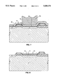
- FIG. 1 is a cross-sectional view of a DRAM cell having a conventional planar capacitor
- FIG. 2 is a cross-sectional view of a DRAM cell having a typical trench capacitor
- FIG. 3 is a cross-sectional view of a DRAM cell having a typical stacked capacitor
- FIG. 4 is a cross-sectional view of a DRAM cell of planar-capacitor design during the fabrication process, subsequent to the creation of the cell's field effect transistor gate and word line from a poly-1 layer and doping of the transistor's storage-node and access-node junction regions;
- FIG. 5 is a cross-sectional view of the DRAM cell of FIG. 4 following the blanket deposition of a thin poly starter layer
- FIG. 6 is a cross-sectional view of the DRAM cell of FIG. 5 following texturization of the substrate regions;
- FIG. 7 is a cross-sectional view of the DRAM cell of FIG. 6 following a silicon dioxide etch, blanket deposition of a silicon nitride layer, deposition of a poly cell plate layer, and masking of the poly field plate layer with a photoresist mask;
- FIG. 8 is a cross-sectional view of the DRAM cell of FIG. 7 following the etching of the poly cell plate layer and the silicon nitride layer;
- FIG. 9 is a cross-sectional view of the DRAM cell of FIG. 8, completed in accordance with conventional processing technology
- FIG. 10 is a cross-sectional view of a polysilicon-starter-layer-covered monosilicon substrate
- FIG. 11 is a cross-sectional view of the monosilicon substrate of FIG. 10 following a wet oxidation that has consumed a portion of the polysilicon starter layer and created texturization thereon;
- FIG. 12 is a cross-sectional view of the monosilicon substrate of FIG. 11 following continued wet oxidation that has consumed the polysilicon starter layer to the point where the oxidation reaction has reached the polysilicon-monosilicon interface;
- FIG. 13 is a cross-sectional view of the monosilicon substrate of FIG. 12 following continued wet oxidation that has entirely consumed the starter layer and a small portion of the substrate, transferring texturization from the starter layer to the substrate;
- FIG. 14 is a cross-sectional view of the monosilicon substrate of FIG. 13 following an oxide etch that has removed the silicon dioxide accumulated during the wet oxidation;
- FIG. 15 is a cross-sectional view of a polysilicon-starter-layer-covered, texturized monosilicon substrate
- FIG. 16 is a cross-sectional view of the texturized monosilicon substrate of FIG. 15 following a wet oxidation that has consumed a portion of the polysilicon starter layer and created texturization thereon;
- FIG. 17 is a cross-sectional view of the texturized monosilicon substrate of FIG. 16 following continued wet oxidation that has consumed the polysilicon starter layer to the point where the oxidation reaction has reached the polysilicon-monosilicon interface;
- FIG. 18 is a cross-sectional view of the texturized monosilicon substrate of FIG. 12 following continued wet oxidation that has entirely consumed the starter layer and a small portion of the texturized substrate, transferring further texturization from the starter layer to the previously texturized substrate;
- FIG. 19 is a cross-sectional view of the texturized monosilicon substrate of FIG. 18 following an oxide etch that has removed the silicon dioxide accumulated during the wet oxidation;
- FIG. 20 is a cross-sectional view of the monosilicon substrate of FIG. 10 following an anisotropic etch which imparts texturization to the polysilicon starter layer;
- FIG. 21 is a cross-sectional view of the monosilicon substrate of FIG. 20 following continued anisotropic etching that has consumed the polysilicon starter layer to the point where the anisotropic etch has reached the polysilicon-monosilicon interface;
- FIG. 22 is a cross-sectional view of the monosilicon substrate of FIG. 21 following continued anisotropic etching that has completely transferred texturization on the polysilicon starter layer to the monosilicon substrate;
- FIG. 23 is a cross-sectional view of the texturized monosilicon substrate of FIG. 15 following an anisotropic etch which imparts texturization to the polysilicon starter layer;
- FIG. 24 is a cross-sectional view of the texturized monosilicon substrate of FIG. 23 following continued anisotropic etching that has consumed the polysilicon starter layer to the point where the anisotropic etch has reached the polysilicon-monosilicon interface;
- FIG. 25 is a cross-sectional view of the texturized monosilicon substrate of FIG. 24 following continued anisotropic etching that has completely transferred further texturization on the polysilicon starter layer to the previously texturized monosilicon substrate;
- FIG. 26 is a cross-sectional view of the monosilicon substrate of FIG. 11 following an oxide etch that has removed oxide that accumulated on the polysilicon starter layer during the wet oxidation thereof;
- FIG. 27 is a cross-sectional view of the monosilicon substrate of FIG. 26 following an anisotropic etch that has consumed the remaining portion of the polysilicon starter layer and a small portion of the monosilicon substrate, thus transferring the texturization pattern from the starter layer to the underlying substrate;
- FIG. 28 is a cross-sectional view of the texturized monosilicon substrate of FIG. 16 following an oxide etch that has removed oxide that accumulated on the polysilicon starter layer during the wet oxidation thereof;
- FIG. 29 is a cross-sectional view of the texturized monosilicon substrate of FIG. 28 following an anisotropic etch that has consumed the remaining portion of the polysilicon starter layer and a small portion of the previously texturized monosilicon substrate, thus transferring the further texturized pattern from the starter layer to the underlying previously texturized substrate.
- a DRAM cell capacitor in accordance with the present invention is described first, with references to FIGS. 4 through 9.
- DRAM cell substrate texturization processes in accordance with the present invention are then described, with references to FIGS. 10 through 29.
- FIG. 4 a DRAM cell of planar design is shown during the early stages of the fabrication process.
- a field effect transistor gate 41 and a word line 42 (the interconnect between FET gates in an array column) have been created from a conductively-doped poly-1 layer.
- Self-aligned heavy doping of a lightly-doped p-type substrate 43 with phosphorus and arsenic has created n-type FET access-node junction 44 and n-type FET storage-node junction 45.
- a cell capacitor will be constructed on the exposed n-type substrate capacitive region 46 that, in FIG. 4, is to the right of storage-node junction 45.
- a bit line will make contact with the exposed n-type substrate bit-line-contact region 47 that is to the left of access-node junction 44.
- the monocrystalline silicon texturization process is begun with the blanket deposition of a polycrystalline silicon poly starter layer 51 of substantially uniform thickness over the surface of the cell.
- the optimum thickness of poly starter layer 51 will be determined by the crystal grain size and dopant concentration of poly starter layer 51.
- a substantially uniform thickness of approximately 1,000-2,000 angstroms will provide good texturization.
- the cell has been subjected to wet oxidation. Since oxidation proceeds more rapidly at crystal grain boundaries than in the center of a crystal, the exposed surface of poly starter layer 51 becomes texturized as oxidation continues. Texturization occurs because the poly etches and oxidizes more rapidly at the crystal grain boundaries within the poly layer. Thus, the surface of the polysilicon starter layer acquires a texturized topography having a granular appearance.
- the polysilicon crystals produce convex surface features, appearing similar to rounded hillocks.
- the crystal grain boundaries, where the etching and oxidation occurs more rapidly, produce concave surface features, appearing similar to valleys.
- the size of the polysilicon crystals determine the sizing and separation of the convex and concave surface features.
- the poly starter layer 51 should be deposited substantially uniformly to avoid planarization of the underlying monocrystalline substrate. If the poly starter layer 51 is not of substantially uniform thickness, surface asperities otherwise produced by the oxidation (or etching as discussed below) at the crystal grain boundaries can be minimized from the resulting nonuniform transfer of the texturization pattern to the underlying substrate.
- silicon dioxide layer 61 has been removed with a wet oxide etch, exposing the textured surfaces of substrate capacitive region 46 and substrate bit-line-contact region 47.
- texturization may also be accomplished using two other, somewhat similar, processes.
- the poly starter layer is etched anisotropically, with consumption of the material occurring more rapidly along the polycrystalline boundaries than in the center of the crystal.
- a texturized surface is created on the poly starter layer.
- the texturized pattern is transferred to the underlying mono substrate.
- a wet oxidation step and a subsequent oxide etch are used to create a texturized surface on the thin poly starter layer.
- An anisotropic etch consumes the poly starter layer and transfers the texture on the poly to the underlying mono layer.
- this texturization of the monosilicon substrate 43 is performed multiple times. Successive, subsequent poly starter layers 51 are deposited and consumed, as described above. Each successive poly starter layer 51 has its own unique crystal grain boundaries which will be randomly superimposed over the unique locations of the respective crystal grain boundaries of the preceding poly starter layers 51. This results in more asperities forming in the surface of the substrate 43, and therefore, greater surface area, as compared to a nontexturized substrate.
- a silicon nitride layer 71 is blanket deposited over the surface of the cell. This is followed with the blanket deposition of a poly-2 cell plate layer 72. Following the doping of poly-2 layer 72 with phosphorus to render it conductive, poly-2 layer 72 is masked with a photoresist mask 73.
- poly-2 layer 72 and silicon nitride layer 71 have been etched to form a cell plate 81, which will function as the cell's field capacitor plate.
- the cell capacitor is now complete.
- a boro-phosphoro-silicate glass (BPSG) layer 91 has been blanket deposited over the surface of the cell.
- BPSG boro-phosphoro-silicate glass
- aluminum metal is blanket deposited over the cell's surface, and then etched to form bit line 93. Blanket deposition of passivation layers 94 follows.
- a first embodiment of the texturization process includes the steps described in FIGS. 10 through 19.
- a polysilicon starter layer 111 having a substantially uniform thickness in the range of approximately 500 to 5,000 angstroms (the optimum thickness is deemed to be approximately 1,000-2,000 angstroms) is deposited on top of a monosilicon substrate 112.
- the boundaries between crystal grains 113 are represented by the broken lines 114.
- the monosilicon substrate 112 and superjacent polysilicon starter layer 111 of FIG. 10 have been subjected to a wet oxidation that has consumed a portion of the polysilicon starter layer 111 and created texturization thereon.
- consumption of the polysilicon starter layer 111 proceeds more rapidly at crystal grain boundaries.
- a layer of silicon dioxide 151 accumulates on top of the textured surface of starter layer 111.
- the monosilicon substrate 112 and superjacent polysilicon starter layer 111 of FIG. 11 are further subjected to wet oxidation, resulting in consumption of the polysilicon starter layer to the point where the oxidation reaction has reached the polysilicon-monosilicon interface 181.
- monocrystalline silicon from substrate 112 is being consumed between the crystal grain boundaries of the remaining portion of polysilicon starter layer 111.
- starter layer has been consumed to the point that only non-contiguous bumps 182 remain on the surface of monosilicon substrate 112.
- Silicon dioxide layer 151 has continued to increase in thickness as silicon is consumed.
- an oxide etch has removed silicon dioxide layer 151, thus exposing the texturized surface of monosilicon substrate 112.
- another polysilicon starter layer 111a having a thickness in the range of approximately 500 to 5,000 angstroms is deposited on top of the texturized monosilicon substrate 112a.
- the boundaries between its crystal grains 113a are represented by the broken lines 114a. Due to the randomness of the locations of the new crystal grains 113a, their boundaries 114a may not necessarily be superimposed over the corresponding locations of the crystal grain boundaries 114 of the preceding starter layer 111.
- the texturized substrate 112a and superjacent polysilicon starter layer 111a of FIG. 15 have been subjected to a wet oxidation that has consumed a portion of the polysilicon starter layer 111a and created texturization thereon. Again, consumption of the polysilicon starter layer 111a proceeds more rapidly at crystal grain boundaries 114a. As the wet oxidation consumes polysilicon starter layer 111a, a layer of silicon dioxide 151a accumulates on top of the textured surface of starter layer 111a.
- the texturized substrate 112a and superjacent polysilicon starter layer 111a of FIG. 16 are further subjected to wet oxidation, resulting in consumption of the polysilicon starter layer 111a to the point where the oxidation reaction has reached the polysilicon-monosilicon interface 181a.
- monocrystalline silicon from substrate 112a is being consumed between the crystal grain boundaries 114a of the remaining portion of polysilicon starter layer 111a.
- the starter layer 111a has been consumed to the point that only non-contiguous bumps 182a remain on the surface of monosilicon substrate 112a.
- Silicon dioxide layer 151a has continued to increase in thickness as silicon is consumed.
- sizing and separation of these surface asperities are dependent upon the size of the polysilicon crystals. Typical sizes of such crystals are approximately 0.1-0.2 microns. Therefore, after the initial texturization, typical sizing and separation of the surface asperities will be 0.1-0.2 microns. Following subsequent texturizations, their typical sizing and separation will be less than 0.1 microns.
- Simko discloses electrodes of singly texturized polysilicon for an electrically erasable, programmable read-only memory (EEPROM).
- EEPROM electrically erasable, programmable read-only memory
- Simko's singly texturized polysilicon has surface asperities with an approximate areal density of 5 ⁇ 10 9 per square centimeter (cm 2 ), an average base width of 456 angstroms ( ⁇ ) and an average height of 762 angstroms.
- an oxide etch has removed silicon dioxide layer 151a, thus exposing the further texturized surface of the previously texturized substrate 112a.
- a second embodiment of the texturization process begins with FIG. 10 and includes the steps described in FIGS. 20 through 25.
- polysilicon starter layer 111 (of FIG. 10) has been subjected to an anisotropic etch, which causes the surface of polysilicon starter layer 111 to develop a multitude of bumps 121, which equate to a texturized surface.
- the texturized surface develops because the polysilicon etches more rapidly at the boundaries 114 of the crystal grains 113 than in their centers.
- the anisotropic etch is continued until the polysilicon starter layer 111 has been consumed to the point where the etch has reached the polysilicon-monosilicon interface 131. At this point, monocrystalline silicon from substrate 112 is being consumed between the crystal grain boundaries of the remaining portion of polysilicon starter layer 111. In this representation, starter layer 111 has been consumed to the point that only noncontiguous bumps 132 remain on the surface of monosilicon substrate 112.
- the anisotropic etch is continued still further until the polysilicon starter layer 111 has been entirely etched away, thus transferring the texturization that was previously on starter layer 111 to the underlying substrate 112.
- another polysilicon starter layer 111a has been subjected to another anisotropic etch, which causes the surface of polysilicon starter layer 111a to develop another multitude of bumps 121a, which equate to another texturized surface.
- the texturized surface develops because the polysilicon etches more rapidly at the boundaries 114a of the crystal grains 113a than in their centers.
- the anisotropic etch is continued until the polysilicon starter layer 111a has been consumed to the point where the etch has reached the polysilicon-monosilicon interface 131a. At this point, monocrystalline silicon from the previously texturized substrate 112a is being consumed between the crystal grain boundaries 114a of the remaining portion of the polysilicon starter layer 111a. In this representation, the starter layer 111a has been consumed to the point that only noncontiguous bumps 132a remain on the surface of the texturized substrate 112a.
- the anisotropic etch is continued still further until the polysilicon starter layer 111a has been entirely etched away, thus transferring the texturization that was previously on the starter layer 111a to the underlying previously texturized substrate 112a.
- a third embodiment of the texturization process begins with FIG. 10, includes the step described in FIGS. 11 and 16, and then further encompasses the steps described in FIGS. 26 through 29.
- silicon dioxide layer 151 (of FIG. 11) has been removed with an oxide etch, exposing the texturized surface of polysilicon starter layer 111.
- an anisotropic etch has consumed the remaining portion of the polysilicon starter layer 111 and a small portion of the monosilicon substrate 112, thus transferring the texturization pattern from the starter layer to the underlying substrate.
- silicon dioxide layer 151a (of FIG. 16) has been removed with an oxide etch, exposing the texturized surface of polysilicon starter layer 111a.
- an anisotropic etch has consumed the remaining portion of the polysilicon starter layer 111a and a small portion of the previously texturized substrate 112a, thus transferring the texturization pattern from the starter layer 111a to the underlying substrate 112a.
Abstract
A DRAM cell having a doped monocrystalline silicon substrate for the cell's lower capacitor plate whose surface has been texturized multiple times to enhance cell capacitance. After texturization, a thin silicon nitride layer is deposited on top of the texturized substrate, followed by the deposition of a poly layer, which functions as the cell's upper, or field, capacitor plate. The nitride layer, conformal and thin compared to the surface texture of the mono substrate, transfers the texture of the substrate to the cell plate layer. The effective capacitor plate area is substantially augmented, resulting in a cell capacitance increase of at least approximately fifty percent compared to a conventional planar cell utilizing identical wafer area. The substrate is texturized by texturizing a thin polycrystalline silicon (poly) starter layer that has been deposited on top of the substrate by using an anisotropic etch or wet oxidation step, and then allowing the poly starter layer to be consumed, transferring the texture created on the poly starter layer to the underlying substrate. By subjecting the starter layer to either an etch or an oxidation step, atoms at the grain boundaries of the starter layer react more rapidly, thus establishing the texturization pattern. Once established, the starter layer's texturization pattern is transferred to the monocrystalline silicon surface by either etching or oxidizing the starter layer. Performing this texturization process multiple times produces greater texturization due to the consumption of the successive poly starter layers along their respective, uniquely superimposed grain boundaries.
Description
This case is a continuation-in-part of patent applications having Ser. Nos. 07/465,692 and 07/465,693, both filed on Jan. 16, 1990.
1. Field of the Invention
This invention relates to semiconductor technology and, more specifically, to the design of capacitors used in dynamic random access memory (DRAM) cells. The focus of the invention is upon processes for imparting a texturized surface to a doped monocrystalline silicon substrate that is used for a planar DRAM cell's lower capacitor plate in order to increase the capacitance of the cell.
2. Description of the Related Art
The memory cells of dynamic random access memories are comprised of two main components: a field-effect transistor and a capacitor. In DRAM cells utilizing a conventional planar capacitor (such as the one depicted in FIG. 1), far more chip surface area is dedicated to planar capacitor 11 than to field-effect transistor (FET) 12. The gate 13 of FET 12 and the word line 14 are formed from an etched polycrystalline silicon-1 layer. Bit line 15 connects with access-node junction 16. Capacitor 11 has a lower (storage-node) plate formed from the n+ silicon substrate extension 17 of storage-node junction 18 of FET 12. Upper capacitor plate (or field plate) 19 is formed from a layer of conductively-doped polycrystalline silicon. Substrate extension 17 is electrically insulated from upper plate 19 by a dielectric layer 20.
Planar capacitors have generally proven adequate for use in DRAM chips up to the one-megabit level. However, planar capacitors constructed with conventional dielectric materials appear to be unusable beyond the one-megabit DRAM level. As component density in memory chips has increased, the shrinkage of cell capacitor size has resulted in a number of problems.
Firstly, the alpha-particle component of normal background radiation will generate hole-electron pairs in the n+ silicon substrate plate of a cell capacitor. This phenomena will cause the charge within the affected cell capacitor to rapidly dissipate, resulting in a "soft" error. Secondly, as cell capacitance is reduced, the sense-amp differential signal is reduced. This aggravates noise sensitivity and makes it more difficult to design a sense-amp having appropriate signal selectivity. Thirdly, as cell capacitance is decreased, the cell refresh time must generally be shortened, thus requiring more frequent interruptions for refresh overhead.
The difficult goal of a DRAM designer is therefore to increase or, at least, maintain cell capacitance as cell size shrinks, without resorting to processes that reduce product yield or that markedly increase the number of masking and deposition steps in the production process. Several methods for providing adequate cell capacitance in the face of shrinking cell size are either in use or under investigation. Basically, the efforts fall into two categories. Efforts within the first category are aimed at creating complex three-dimensional capacitors; those within the second are aimed at improving the dielectric of the planar capacitor.
The three-dimensional technique currently receiving the most attention involves the creation of "trench" capacitors in the cell substrate. FIG. 2 depicts a DRAM cell having a typical trench capacitor 21. Similar in concept to planar capacitor 11 of FIG. 1, the trench is employed to provide greater plate area, and hence, greater capacitance. The storage-node plate 22 may be formed from the n+ doped silicon substrate or it may be formed from a polysilicon layer which lines a trench cut in the n+ doped silicon substrate. The field plate 23 is formed from a layer of conductively-doped polycrystalline silicon. Storage-node plate 22 and field plate 23 are electrically insulated with a dielectric layer 24.
DRAM chips employing trench capacitors have been built by a number of European, Japanese and U.S. companies, including IBM Corporation, Texas Instruments Inc., Nippon Electric Company, Toshiba, Matsushita and Mitsubishi Electric Corporation. There are several problems inherent In the trench design, not the least of which is trench-to-trench capacitive charge leakage which is the result of a parasitic transistor effect between trenches. Another problem is the difficulty of completely cleaning the capacitor trenches during the fabrication process; failure to completely clean a trench will generally result in a defective cell.
Another three-dimensional technique, which is being used by Mitsubishi Electric Company, Hitachi, and Fujitsu Ltd., is the stacking of capacitor plates between dielectric layers on the DRAM cell surface. FIG. 3 is a graphic representation of a typical DRAM cell having a stacked capacitor 31. The lower (storage-node) plate 32 is formed from an n-type polycrystalline silicon layer which is in contact with the silicon substrate 33 in the region of the FET storage-node junction, while the upper (field) plate 34 is formed from a conductively-doped polycrystalline silicon layer. The two layers are separated by a dielectric layer 35. Lower plate 32 and upper plate 34 are both stacked on top of FET 12 and word line 36, resulting in a high-profile cell which requires more stringent process control for the connection of bit line 37 to access-node junction 38.
Alternatively, other schemes involve the use of ferroelectric materials for DRAM cell capacitor dielectrics. Since ferroelectric materials have a dielectric constant more than 100 times that of silicon oxides, the use of such materials has the potential for allowing the size of the DRAM cell capacitor to be shrunk to one of the smaller cell elements without resorting to three-dimensional structures. Critics of ferroelectric materials point out that such materials suffer from a "wearout" mechanism. In addition, they warn that there are many chemical incompatibilities with the other materials used in integrated circuit fabrication and that the layering of ferroelectric films within integrated circuit structures has not yet been done successfully.
In 1986, M. Olcer, H. J. Buhlmann and M. Ilegems described a process for texturizing monocrystalline silicon (hereinafter also "monosilicon" or "mono") in Volume 133 of the Journal of the Electrochemical Society. The process utilizes an anisotropic wet etch to slightly roughen the surface of the monosilicon. Use of monosilicon so textured has been suggested for use in EEPROMs.
A process for texturizing polycrystalline silicon (hereinafter also "polysilicon" or "poly") has been developed by Xicor, Inc. The Xicor process takes advantage of the greater reactivity of silicon atoms at the polysilicon crystal grain boundaries. When subjected to an anisotropic etch or a wet oxidation, the silicon atoms at the crystal grain boundaries are consumed at a faster rate than are those within the crystals. As a result of this differential in consumption rates, a texturization pattern is soon established on the polysilicon, giving it a granular appearance dependent upon the size of the polysilicon crystals.
Xicor has used texturized polysilicon to increase electron injection during write and erase operations in electrically-erasable programmable read-only memory (EEPROM) cells. During EEPROM construction, texturization is followed by thermal oxidation of the texturized surface. The bumps on the surface of the poly create regions of increased electric field strength, which both lowers breakdown voltage of the thermally-grown silicon dioxide and enhances current leakage by several orders of magnitude. In this application, the thermally-grown silicon dioxide, in which conduction is electrode limited in accordance with what is known as the Fowler-Nordheim mechanism, functions as a tunneling layer.
Texturized polysilicon has also been used by the instant inventors to increase capacitance of DRAM cells. In order to avoid the tunneling effect--useful for the Xicor-developed EEPROM memories, but certain to cause information-destroying low-voltage breakdown in a DRAM cell--the use of a thin-layer silicon dioxide dielectric between two roughened or texturized surfaces is precluded. However, dielectrics such as silicon nitride or tantalum pentoxide, which demonstrate bulk-limited conduction, most likely in accordance with what is known as the Frankel-Poole mechanism, are much more suitable as thin-layer dielectrics for use in DRAMs where capacitive layers are not smooth.
Since the polysilicon texturization is only applicable to DRAM memories which utilize a polysilicon for storage-node capacitor plates, the process is unusable for other DRAM memories. For example, planar DRAM memory arrays are typically constructed on a monocrystalline silicon (hereinafter also "monosilicon" or "mono") substrate and utilize the substrate for the storage-node capacitor plates. Since there are no crystal boundaries within such arrays, it would be impossible to achieve texturization of the monosilicon substrate through direct use of the etch or oxidation method that has been developed for the texturization of polysilicon. A process for texturizing monocrystalline silicon would clearly be useful.
The present invention is applicable primarily to dynamic random access memories (DRAMs) which utilize planar capacitor cell designs. Typically, planar DRAM cell capacitors employ a portion of the monocrystalline silicon (hereinafter also "mono") substrate, that is an extension of the cell's FET storage-node junction, for the capacitor's storage-node plate.
A texturization process, which uses a thin superjacent polycrystalline silicon (hereinafter also "poly") starter layer, is employed for texturizing a monocrystalline silicon substrate to create a three-dimensional texturized surface on the upper surface of the mono substrate. Following the deposition of a polycrystalline silicon starter layer of substantially uniform thickness on top of the monosilicon substrate, the polysilicon starter layer is anisotropically etched or oxidized to create a texturization pattern on the starter layer.
The texturization pattern develops because the poly etches and oxidizes more rapidly at the crystal grain boundaries within the poly layer. Thus, the surface of the polysilicon starter layer acquires a texturized topography having a granular appearance. The polysilicon crystals produce convex surface features, appearing similar to rounded hillocks. The crystal grain boundaries, where the etching and oxidation occurs more rapidly, produce concave surface features, appearing similar to valleys. The size of the polysilicon crystals determine the sizing and separation of the convex and concave surface features.
Once a pattern is established on the starter layer, it may be transferred to the underlying mono substrate by utilizing either an anisotropic etch or a wet oxidation to consume the balance of the starter layer. Since the silicon consumption reaction (whether it be wet oxidation or anisotropic etch) reaches the poly-mono interface at the poly crystal grain boundaries first, maximum transfer of the pattern has transferred to the underlying mono silicon as soon as the last remnant of the poly starter layer is consumed.
In order to maximize texturization on the underlying mono silicon, it is important that the consumption reaction be halted as soon as consumption of the starter layer is complete. Otherwise, the degree of texturization will begin to diminish as the natural tendency toward greater entropy works to smooth the textured surface. If oxidation has been employed to consume the starter layer and the small portion of the mono silicon layer necessary to transfer the texturization thereto, an oxide etch of the mono substrate is required to remove accumulated silicon dioxide, thus exposing the texturized mono surface.
This texturization process is repeated to further texturize the mono substrate. Another polycrystalline silicon starter layer of substantially uniform thickness is deposited on top of the monosilicon substrate and anisotropically etched or oxidized to create a new texturization pattern on the new starter layer. As before, the new texturization pattern develops because the poly etches and oxidizes more rapidly at the crystal grain boundaries within the poly layer.
However, the subsequent poly starter layer's uniquely and randomly distributed crystal grain boundaries are not aligned with those of the preceding poly starter layer. Therefore, the etching or oxidation produces a consumption reaction which reaches the poly-mono interface at the new poly crystal grain boundaries first, thereby transferring the new texturization pattern to the already texturized underlying mono silicon. This repeated texturization produces further substrate surface asperities, which in turn, increase the effective surface area available for the capacitor plates of the DRAM cell.
Monosilicon texturized in accordance with the present invention may be used in a variety of applications. For example, it may be used to increase electron injection in EEPROMs and may also be used to increase DRAM cell capacitance.
With multiple texturization complete, a thin (70-100 angstroms thick) silicon nitride layer is deposited on top of the texturized mono substrate, followed by the deposition of a cell plate poly layer, which functions as the upper, or field, capacitor plate. Since the nitride layer is conformal in nature, and thin in comparison to the bumps on the surface of the monocrystalline silicon substrate, the texture of the substrate is transferred through the silicon nitride layer to the cell plate layer. The effective capacitive plate area is substantially augmented, resulting in a cell capacitance increase of at least approximately fifty percent in comparison to a conventional planar cell utilizing identical wafer surface area.
Because conduction in silicon dioxide is electrode limited, generally considered to be in accordance with what is known as the Fowler-Nordheim mechanism, the use of thin layers of silicon dioxide as a DRAM cell dielectric between two roughened surfaces is precluded, since low-voltage breakdown is likely. However, because conduction in silicon nitride is bulk limited, most likely in accordance with what is known as the Frankel-Poole mechanism, silicon nitride is a much more suitable thin layer dielectric for use in DRAMs where capacitive layers are not smooth.
Throughout the figures, similar elements are designated by similar reference numerals.
FIGS. 1 through 3 depict existing technologies. FIGS. 4 through 9 depict the fabrication of a DRAM array having a capacitor design conforming to the present invention. FIGS. 10 through 29 depict processes for texturizing a DRAM substrate to fabricate a DRAM array having a capacitor design conforming to the present invention.
FIG. 1 is a cross-sectional view of a DRAM cell having a conventional planar capacitor;
FIG. 2 is a cross-sectional view of a DRAM cell having a typical trench capacitor;
FIG. 3 is a cross-sectional view of a DRAM cell having a typical stacked capacitor;
FIG. 4 is a cross-sectional view of a DRAM cell of planar-capacitor design during the fabrication process, subsequent to the creation of the cell's field effect transistor gate and word line from a poly-1 layer and doping of the transistor's storage-node and access-node junction regions;
FIG. 5 is a cross-sectional view of the DRAM cell of FIG. 4 following the blanket deposition of a thin poly starter layer;
FIG. 6 is a cross-sectional view of the DRAM cell of FIG. 5 following texturization of the substrate regions;
FIG. 7 is a cross-sectional view of the DRAM cell of FIG. 6 following a silicon dioxide etch, blanket deposition of a silicon nitride layer, deposition of a poly cell plate layer, and masking of the poly field plate layer with a photoresist mask; and
FIG. 8 is a cross-sectional view of the DRAM cell of FIG. 7 following the etching of the poly cell plate layer and the silicon nitride layer;
FIG. 9 is a cross-sectional view of the DRAM cell of FIG. 8, completed in accordance with conventional processing technology;
FIG. 10 is a cross-sectional view of a polysilicon-starter-layer-covered monosilicon substrate;
FIG. 11 is a cross-sectional view of the monosilicon substrate of FIG. 10 following a wet oxidation that has consumed a portion of the polysilicon starter layer and created texturization thereon;
FIG. 12 is a cross-sectional view of the monosilicon substrate of FIG. 11 following continued wet oxidation that has consumed the polysilicon starter layer to the point where the oxidation reaction has reached the polysilicon-monosilicon interface;
FIG. 13 is a cross-sectional view of the monosilicon substrate of FIG. 12 following continued wet oxidation that has entirely consumed the starter layer and a small portion of the substrate, transferring texturization from the starter layer to the substrate;
FIG. 14 is a cross-sectional view of the monosilicon substrate of FIG. 13 following an oxide etch that has removed the silicon dioxide accumulated during the wet oxidation;
FIG. 15 is a cross-sectional view of a polysilicon-starter-layer-covered, texturized monosilicon substrate;
FIG. 16 is a cross-sectional view of the texturized monosilicon substrate of FIG. 15 following a wet oxidation that has consumed a portion of the polysilicon starter layer and created texturization thereon;
FIG. 17 is a cross-sectional view of the texturized monosilicon substrate of FIG. 16 following continued wet oxidation that has consumed the polysilicon starter layer to the point where the oxidation reaction has reached the polysilicon-monosilicon interface;
FIG. 18 is a cross-sectional view of the texturized monosilicon substrate of FIG. 12 following continued wet oxidation that has entirely consumed the starter layer and a small portion of the texturized substrate, transferring further texturization from the starter layer to the previously texturized substrate;
FIG. 19 is a cross-sectional view of the texturized monosilicon substrate of FIG. 18 following an oxide etch that has removed the silicon dioxide accumulated during the wet oxidation;
FIG. 20 is a cross-sectional view of the monosilicon substrate of FIG. 10 following an anisotropic etch which imparts texturization to the polysilicon starter layer;
FIG. 21 is a cross-sectional view of the monosilicon substrate of FIG. 20 following continued anisotropic etching that has consumed the polysilicon starter layer to the point where the anisotropic etch has reached the polysilicon-monosilicon interface;
FIG. 22 is a cross-sectional view of the monosilicon substrate of FIG. 21 following continued anisotropic etching that has completely transferred texturization on the polysilicon starter layer to the monosilicon substrate;
FIG. 23 is a cross-sectional view of the texturized monosilicon substrate of FIG. 15 following an anisotropic etch which imparts texturization to the polysilicon starter layer;
FIG. 24 is a cross-sectional view of the texturized monosilicon substrate of FIG. 23 following continued anisotropic etching that has consumed the polysilicon starter layer to the point where the anisotropic etch has reached the polysilicon-monosilicon interface;
FIG. 25 is a cross-sectional view of the texturized monosilicon substrate of FIG. 24 following continued anisotropic etching that has completely transferred further texturization on the polysilicon starter layer to the previously texturized monosilicon substrate;
FIG. 26 is a cross-sectional view of the monosilicon substrate of FIG. 11 following an oxide etch that has removed oxide that accumulated on the polysilicon starter layer during the wet oxidation thereof;
FIG. 27 is a cross-sectional view of the monosilicon substrate of FIG. 26 following an anisotropic etch that has consumed the remaining portion of the polysilicon starter layer and a small portion of the monosilicon substrate, thus transferring the texturization pattern from the starter layer to the underlying substrate;
FIG. 28 is a cross-sectional view of the texturized monosilicon substrate of FIG. 16 following an oxide etch that has removed oxide that accumulated on the polysilicon starter layer during the wet oxidation thereof; and
FIG. 29 is a cross-sectional view of the texturized monosilicon substrate of FIG. 28 following an anisotropic etch that has consumed the remaining portion of the polysilicon starter layer and a small portion of the previously texturized monosilicon substrate, thus transferring the further texturized pattern from the starter layer to the underlying previously texturized substrate.
A DRAM cell capacitor in accordance with the present invention is described first, with references to FIGS. 4 through 9. DRAM cell substrate texturization processes in accordance with the present invention are then described, with references to FIGS. 10 through 29.
Referring now to FIG. 4, a DRAM cell of planar design is shown during the early stages of the fabrication process. A field effect transistor gate 41 and a word line 42 (the interconnect between FET gates in an array column) have been created from a conductively-doped poly-1 layer. Self-aligned heavy doping of a lightly-doped p-type substrate 43 with phosphorus and arsenic has created n-type FET access-node junction 44 and n-type FET storage-node junction 45. A cell capacitor will be constructed on the exposed n-type substrate capacitive region 46 that, in FIG. 4, is to the right of storage-node junction 45. A bit line will make contact with the exposed n-type substrate bit-line-contact region 47 that is to the left of access-node junction 44.
Referring now to FIG. 5, the monocrystalline silicon texturization process is begun with the blanket deposition of a polycrystalline silicon poly starter layer 51 of substantially uniform thickness over the surface of the cell. The optimum thickness of poly starter layer 51 will be determined by the crystal grain size and dopant concentration of poly starter layer 51. A substantially uniform thickness of approximately 1,000-2,000 angstroms will provide good texturization.
Referring now to FIG. 6, the cell has been subjected to wet oxidation. Since oxidation proceeds more rapidly at crystal grain boundaries than in the center of a crystal, the exposed surface of poly starter layer 51 becomes texturized as oxidation continues. Texturization occurs because the poly etches and oxidizes more rapidly at the crystal grain boundaries within the poly layer. Thus, the surface of the polysilicon starter layer acquires a texturized topography having a granular appearance. The polysilicon crystals produce convex surface features, appearing similar to rounded hillocks. The crystal grain boundaries, where the etching and oxidation occurs more rapidly, produce concave surface features, appearing similar to valleys. The size of the polysilicon crystals determine the sizing and separation of the convex and concave surface features.
As poly starter layer 51 becomes consumed, the texture thereon is transferred to the underlying monocrystalline substrate. The wet oxidation step may be terminated as soon as poly starter layer 51 has been entirely consumed. At that point, maximum transfer of texturization will have occurred. As a result of the oxidation of poly starter layer 51 and portions of both underlying substrate regions 46 and 47, silicon dioxide layer 61 has grown on top of both substrate region 46 and 47.
The poly starter layer 51 should be deposited substantially uniformly to avoid planarization of the underlying monocrystalline substrate. If the poly starter layer 51 is not of substantially uniform thickness, surface asperities otherwise produced by the oxidation (or etching as discussed below) at the crystal grain boundaries can be minimized from the resulting nonuniform transfer of the texturization pattern to the underlying substrate.
Referring now to FIG. 7, silicon dioxide layer 61 has been removed with a wet oxide etch, exposing the textured surfaces of substrate capacitive region 46 and substrate bit-line-contact region 47.
Although the texturization process just described appears to be the most controllable means of imparting a texture to a monocrystalline substrate, texturization may also be accomplished using two other, somewhat similar, processes. Using the first alternative method, the poly starter layer is etched anisotropically, with consumption of the material occurring more rapidly along the polycrystalline boundaries than in the center of the crystal. Thus, a texturized surface is created on the poly starter layer. When the poly layer has been entirely consumed, the texturized pattern is transferred to the underlying mono substrate.
Using the second alternative method, a wet oxidation step and a subsequent oxide etch are used to create a texturized surface on the thin poly starter layer. An anisotropic etch consumes the poly starter layer and transfers the texture on the poly to the underlying mono layer.
As discussed more fully below, this texturization of the monosilicon substrate 43 is performed multiple times. Successive, subsequent poly starter layers 51 are deposited and consumed, as described above. Each successive poly starter layer 51 has its own unique crystal grain boundaries which will be randomly superimposed over the unique locations of the respective crystal grain boundaries of the preceding poly starter layers 51. This results in more asperities forming in the surface of the substrate 43, and therefore, greater surface area, as compared to a nontexturized substrate.
In any case, once the texturization process has been completed, a silicon nitride layer 71, approximately 70-100 angstroms thick, is blanket deposited over the surface of the cell. This is followed with the blanket deposition of a poly-2 cell plate layer 72. Following the doping of poly-2 layer 72 with phosphorus to render it conductive, poly-2 layer 72 is masked with a photoresist mask 73.
Referring now to FIG. 8, poly-2 layer 72 and silicon nitride layer 71 have been etched to form a cell plate 81, which will function as the cell's field capacitor plate. The cell capacitor is now complete.
Referring now to FIG. 9, the cell (as well as the entire array of which the cell is but a small part) has been completed in a conventional manner. A boro-phosphoro-silicate glass (BPSG) layer 91 has been blanket deposited over the surface of the cell. Following an oxide etch which exposes a bit-line contact point at the FET access-node junction region 92, aluminum metal is blanket deposited over the cell's surface, and then etched to form bit line 93. Blanket deposition of passivation layers 94 follows.
A first embodiment of the texturization process includes the steps described in FIGS. 10 through 19.
Referring now to FIG. 10, a polysilicon starter layer 111 having a substantially uniform thickness in the range of approximately 500 to 5,000 angstroms (the optimum thickness is deemed to be approximately 1,000-2,000 angstroms) is deposited on top of a monosilicon substrate 112. The boundaries between crystal grains 113 are represented by the broken lines 114.
Referring now to FIG. 11, the monosilicon substrate 112 and superjacent polysilicon starter layer 111 of FIG. 10 have been subjected to a wet oxidation that has consumed a portion of the polysilicon starter layer 111 and created texturization thereon. As discussed more fully below for FIG. 20 with the anisotropic etch, consumption of the polysilicon starter layer 111 proceeds more rapidly at crystal grain boundaries. As the wet oxidation consumes polysilicon starter layer 111, a layer of silicon dioxide 151 accumulates on top of the textured surface of starter layer 111.
Referring now to FIG. 12, the monosilicon substrate 112 and superjacent polysilicon starter layer 111 of FIG. 11 are further subjected to wet oxidation, resulting in consumption of the polysilicon starter layer to the point where the oxidation reaction has reached the polysilicon-monosilicon interface 181. At this point, monocrystalline silicon from substrate 112 is being consumed between the crystal grain boundaries of the remaining portion of polysilicon starter layer 111. In this representation, starter layer has been consumed to the point that only non-contiguous bumps 182 remain on the surface of monosilicon substrate 112. Silicon dioxide layer 151 has continued to increase in thickness as silicon is consumed.
Referring now to FIG. 13, further oxidation of monosilicon substrate 112 and superjacent polysilicon starter layer 111 has resulted in the consumption of the entire starter layer 111 and a small portion of substrate 112, transferring texturization from starter layer 111 to substrate 112. Silicon dioxide layer 151 has become even thicker.
Referring now to FIG. 14, an oxide etch has removed silicon dioxide layer 151, thus exposing the texturized surface of monosilicon substrate 112.
Referring now to FIG. 15, another polysilicon starter layer 111a having a thickness in the range of approximately 500 to 5,000 angstroms is deposited on top of the texturized monosilicon substrate 112a. The boundaries between its crystal grains 113a are represented by the broken lines 114a. Due to the randomness of the locations of the new crystal grains 113a, their boundaries 114a may not necessarily be superimposed over the corresponding locations of the crystal grain boundaries 114 of the preceding starter layer 111.
Referring now to FIG. 16, the texturized substrate 112a and superjacent polysilicon starter layer 111a of FIG. 15 have been subjected to a wet oxidation that has consumed a portion of the polysilicon starter layer 111a and created texturization thereon. Again, consumption of the polysilicon starter layer 111a proceeds more rapidly at crystal grain boundaries 114a. As the wet oxidation consumes polysilicon starter layer 111a, a layer of silicon dioxide 151a accumulates on top of the textured surface of starter layer 111a.
Referring now to FIG. 17, the texturized substrate 112a and superjacent polysilicon starter layer 111a of FIG. 16 are further subjected to wet oxidation, resulting in consumption of the polysilicon starter layer 111a to the point where the oxidation reaction has reached the polysilicon-monosilicon interface 181a. At this point, monocrystalline silicon from substrate 112a is being consumed between the crystal grain boundaries 114a of the remaining portion of polysilicon starter layer 111a. In this representation, the starter layer 111a has been consumed to the point that only non-contiguous bumps 182a remain on the surface of monosilicon substrate 112a. Silicon dioxide layer 151a has continued to increase in thickness as silicon is consumed.
Referring now to FIG. 18, further oxidation of texturized substrate 112a and superjacent polysilicon starter layer 111a has resulted in the consumption of the entire new starter layer 111a and a small portion of substrate 112a, transferring additional texturization from the starter layer 111a to the previously texturized substrate 112a. Silicon dioxide layer 151a has become even thicker.
Thus, as consumption of the new polysilicon starter layer 111a is completed, consumption of the texturized substrate 112a occurs along the new crystal grain boundaries 114a, i.e. between the old crystal grain boundaries 114. This produces more asperities per unit area, and therefore, more surface area, i.e. more exposed surface per unit area of substrate 112a.
The sizing and separation of these surface asperities, e.g. convex and concave substrate surface features, are dependent upon the size of the polysilicon crystals. Typical sizes of such crystals are approximately 0.1-0.2 microns. Therefore, after the initial texturization, typical sizing and separation of the surface asperities will be 0.1-0.2 microns. Following subsequent texturizations, their typical sizing and separation will be less than 0.1 microns.
This is consistent with the sizing and separation of polysilicon surface asperities disclosed by Simko in U.S. Pat. No. 4,300,212. Simko discloses electrodes of singly texturized polysilicon for an electrically erasable, programmable read-only memory (EEPROM). Simko's singly texturized polysilicon has surface asperities with an approximate areal density of 5×10⁹ per square centimeter (cm2), an average base width of 456 angstroms (Å) and an average height of 762 angstroms.
Referring now to FIG. 19, an oxide etch has removed silicon dioxide layer 151a, thus exposing the further texturized surface of the previously texturized substrate 112a.
A second embodiment of the texturization process begins with FIG. 10 and includes the steps described in FIGS. 20 through 25.
Referring now to FIG. 20, polysilicon starter layer 111 (of FIG. 10) has been subjected to an anisotropic etch, which causes the surface of polysilicon starter layer 111 to develop a multitude of bumps 121, which equate to a texturized surface. The texturized surface develops because the polysilicon etches more rapidly at the boundaries 114 of the crystal grains 113 than in their centers.
Referring now to FIG. 21, the anisotropic etch is continued until the polysilicon starter layer 111 has been consumed to the point where the etch has reached the polysilicon-monosilicon interface 131. At this point, monocrystalline silicon from substrate 112 is being consumed between the crystal grain boundaries of the remaining portion of polysilicon starter layer 111. In this representation, starter layer 111 has been consumed to the point that only noncontiguous bumps 132 remain on the surface of monosilicon substrate 112.
Referring now to FIG. 22, the anisotropic etch is continued still further until the polysilicon starter layer 111 has been entirely etched away, thus transferring the texturization that was previously on starter layer 111 to the underlying substrate 112.
Referring now to FIG. 23, another polysilicon starter layer 111a has been subjected to another anisotropic etch, which causes the surface of polysilicon starter layer 111a to develop another multitude of bumps 121a, which equate to another texturized surface. As discussed above, the texturized surface develops because the polysilicon etches more rapidly at the boundaries 114a of the crystal grains 113a than in their centers.
Referring now to FIG. 24, the anisotropic etch is continued until the polysilicon starter layer 111a has been consumed to the point where the etch has reached the polysilicon-monosilicon interface 131a. At this point, monocrystalline silicon from the previously texturized substrate 112a is being consumed between the crystal grain boundaries 114a of the remaining portion of the polysilicon starter layer 111a. In this representation, the starter layer 111a has been consumed to the point that only noncontiguous bumps 132a remain on the surface of the texturized substrate 112a.
Referring now to FIG. 25, the anisotropic etch is continued still further until the polysilicon starter layer 111a has been entirely etched away, thus transferring the texturization that was previously on the starter layer 111a to the underlying previously texturized substrate 112a.
Thus again, consumption of the texturized substrate 112a occurs along the new crystal grain boundaries 114a between the old crystal grain boundaries 114. This produces more substrate 112a surface asperities per unit area, and therefore, more substrate 112a surface area.
A third embodiment of the texturization process begins with FIG. 10, includes the step described in FIGS. 11 and 16, and then further encompasses the steps described in FIGS. 26 through 29.
Referring now to FIG. 26, silicon dioxide layer 151 (of FIG. 11) has been removed with an oxide etch, exposing the texturized surface of polysilicon starter layer 111.
Referring now to FIG. 27, an anisotropic etch has consumed the remaining portion of the polysilicon starter layer 111 and a small portion of the monosilicon substrate 112, thus transferring the texturization pattern from the starter layer to the underlying substrate.
Referring now to FIG. 28, silicon dioxide layer 151a (of FIG. 16) has been removed with an oxide etch, exposing the texturized surface of polysilicon starter layer 111a.
Referring now to FIG. 29, an anisotropic etch has consumed the remaining portion of the polysilicon starter layer 111a and a small portion of the previously texturized substrate 112a, thus transferring the texturization pattern from the starter layer 111a to the underlying substrate 112a.
Thus, as discussed above, consumption of the texturized substrate 112a occurs along the new crystal grain boundaries 114a between the old crystal grain boundaries 114. This produces more substrate 112a surface asperities per unit area, and therefore, more substrate 112a surface area.
It should be understood that the foregoing texturization steps can be further repeated as desired to still further texturize the texturized monosilicon substrate 112a. Repeated texturization will produce still further asperities within the texturized substrate 112a and thereby increase the effective surface areas of the DRAM cell capacitor plates. In turn, these increased plate areas produce a DRAM cell capacitor with enhanced capacitance.
Although only several embodiments of the present invention have been described, it will be apparent to one skilled in the art that changes and modifications may be made thereto without departing from the spirit and the scope of the invention as claimed.
Claims (12)
1. A method of fabricating a memory cell storage capacitor, comprising the steps of:
(a) conductively doping a region within a layer of silicon support material adjacent to a surface thereof;
(b) texturizing said silicon layer surface a plurality of times to produce a texturization pattern thereof by:
(i) depositing a layer of polysilicon of substantially uniform thickness as a sacrificial material upon said silicon layer surface, said polysilicon layer having an exposed surface;
(ii) texturizing said exposed polysilicon surface;
(iii) consuming substantially all of said polysilicon layer; and
(iv) repeating steps (i) through (iv) at least once;
(c) depositing a substantially conformal layer of dielectric material of substantially uniform thickness upon said texturized surface, said dielectric layer being sufficiently thin to allow said texturization pattern to transfer therethrough;
(d) depositing a substantially conformal layer of polysilicon upon said layer of dielectric material;
(e) conductively doping said conformal polysilicon layer.
2. A method as recited in claim 1, wherein said step of (ii) texturizing said exposed polysilicon surface comprises subjecting said exposed polysilicon surface to wet oxidation.
3. A method as recited in claim 2, wherein said step of (iii) consuming substantially all of said polysilicon layer comprises continuing said wet oxidation of said exposed polysilicon surface.
4. A method as recited in claim 2, wherein said step of (iii) consuming substantially all of said polysilicon layer comprises anisotropically etching said exposed polysilicon surface.
5. A method as recited in claim 1, wherein said step of (ii) texturizing said exposed polysilicon surface comprises anisotropically etching said exposed polysilicon surface.
6. A method as recited in claim 5, wherein said step of (iii) consuming substantially all of said polysilicon layer comprising continuing said anisotropically etching of said exposed polysilicon surface.
7. A process for texturizing a surface of monocrystalline silicon, comprising the steps of:
(a) depositing a layer of polysilicon of substantially uniform thickness upon said silicon surface, said polysilicon layer having an exposed surface;
(b) texturizing said exposed polysilicon surface;
(c) comsuming substantially all of said polysilicon layer; and
(d) repeating the foregoing steps at least once.
8. A process as recited in claim 7, wherein said step of (b) texturizing said exposed polysilicon surface comprises subjecting said exposed polysilicon surface to wet oxidation.
9. A process as recited in claim 8, wherein said step of (c) comsuming substantially all of said polysilicon layer comprises continuing said wet oxidation of said exposed polysilicon surface.
10. A process as recited in claim 8, wherein said step of (c) comsuming substantially all of said polysilicon layer comprises anisotropically etching said exposed polysilicon surface.
11. A process as recited in claim 7, wherein said step of (b) texturizing said exposed polysilicon surface comprises anisotropically etching said exposed polysilicon surface.
12. A process as recited in claim 11, wherein said step of (c) comsuming substantially all of said polysilicon layer comprises continuing said anisotropically etching of said exposed polysilicon surface.
Priority Applications (1)
| Application Number | Priority Date | Filing Date | Title |
|---|---|---|---|
| US07/603,528 US5208176A (en) | 1990-01-16 | 1990-10-25 | Method of fabricating an enhanced dynamic random access memory (DRAM) cell capacitor using multiple polysilicon texturization |
Applications Claiming Priority (3)
| Application Number | Priority Date | Filing Date | Title |
|---|---|---|---|
| US46569390A | 1990-01-16 | 1990-01-16 | |
| US46569290A | 1990-01-16 | 1990-01-16 | |
| US07/603,528 US5208176A (en) | 1990-01-16 | 1990-10-25 | Method of fabricating an enhanced dynamic random access memory (DRAM) cell capacitor using multiple polysilicon texturization |
Related Parent Applications (2)
| Application Number | Title | Priority Date | Filing Date |
|---|---|---|---|
| US46569390A Continuation-In-Part | 1990-01-16 | 1990-01-16 | |
| US46569290A Continuation-In-Part | 1990-01-16 | 1990-01-16 |
Publications (1)
| Publication Number | Publication Date |
|---|---|
| US5208176A true US5208176A (en) | 1993-05-04 |
Family
ID=27412956
Family Applications (1)
| Application Number | Title | Priority Date | Filing Date |
|---|---|---|---|
| US07/603,528 Expired - Lifetime US5208176A (en) | 1990-01-16 | 1990-10-25 | Method of fabricating an enhanced dynamic random access memory (DRAM) cell capacitor using multiple polysilicon texturization |
Country Status (1)
| Country | Link |
|---|---|
| US (1) | US5208176A (en) |
Cited By (20)
| Publication number | Priority date | Publication date | Assignee | Title |
|---|---|---|---|---|
| US5340768A (en) * | 1989-12-26 | 1994-08-23 | Texas Instruments Incorporated | Method of fabricating self-aligned field-plate isolation between control electrodes |
| US5414636A (en) * | 1991-06-07 | 1995-05-09 | Fujitsu Limited | Semiconductor memory device having a memory cell capacitor and a fabrication process thereof |
| US5429972A (en) * | 1994-05-09 | 1995-07-04 | Advanced Micro Devices, Inc. | Method of fabricating a capacitor with a textured polysilicon interface and an enhanced dielectric |
| US5629228A (en) * | 1992-07-23 | 1997-05-13 | Texas Instruments Incorporated | Method of making stacked DRAM capacitor structure by using a conformal conductor |
| US5801104A (en) * | 1995-10-24 | 1998-09-01 | Micron Technology, Inc. | Uniform dielectric film deposition on textured surfaces |
| US5872033A (en) * | 1994-03-11 | 1999-02-16 | Micron Technology, Inc. | Method for increasing capacitance of an HSG rugged capacitor using a phosphine rich oxidation and subsequent wet etch |
| US5872376A (en) * | 1997-03-06 | 1999-02-16 | Advanced Micro Devices, Inc. | Oxide formation technique using thin film silicon deposition |
| US5882993A (en) * | 1996-08-19 | 1999-03-16 | Advanced Micro Devices, Inc. | Integrated circuit with differing gate oxide thickness and process for making same |
| US5917213A (en) * | 1997-08-21 | 1999-06-29 | Micron Technology, Inc. | Depletion compensated polysilicon electrodes |
| US5937310A (en) * | 1996-04-29 | 1999-08-10 | Advanced Micro Devices, Inc. | Reduced bird's beak field oxidation process using nitrogen implanted into active region |
| US5962914A (en) * | 1998-01-14 | 1999-10-05 | Advanced Micro Devices, Inc. | Reduced bird's beak field oxidation process using nitrogen implanted into active region |
| US6033943A (en) * | 1996-08-23 | 2000-03-07 | Advanced Micro Devices, Inc. | Dual gate oxide thickness integrated circuit and process for making same |
| US6048763A (en) * | 1997-08-21 | 2000-04-11 | Micron Technology, Inc. | Integrated capacitor bottom electrode with etch stop layer |
| US6259130B1 (en) * | 1998-03-06 | 2001-07-10 | Texas Instruments - Acer Incorporated | High density flash memories with high capacitive-couping ratio and high speed operation |
| WO2002045131A2 (en) * | 2000-11-28 | 2002-06-06 | Infineon Technologies North America Corp. | Process flow for capacitance enhancement in a dram trench |
| US6476432B1 (en) | 2000-03-23 | 2002-11-05 | Micron Technology, Inc. | Structures and methods for enhancing capacitors in integrated circuits |
| US20030042465A1 (en) * | 2001-08-30 | 2003-03-06 | Micron Technology, Inc. | Etchant gas composition |
| US6531364B1 (en) | 1998-08-05 | 2003-03-11 | Advanced Micro Devices, Inc. | Advanced fabrication technique to form ultra thin gate dielectric using a sacrificial polysilicon seed layer |
| US6551940B1 (en) | 1997-04-30 | 2003-04-22 | Micron Technology, Inc. | Undoped silicon dioxide as etch mask for patterning of doped silicon dioxide |
| US6618847B1 (en) * | 1998-11-13 | 2003-09-09 | Stmicroelectronics, Inc. | Power stabilizer using under-utilized standard cells |
Citations (13)
| Publication number | Priority date | Publication date | Assignee | Title |
|---|---|---|---|---|
| US460453A (en) * | 1891-09-29 | Bicycle | ||
| JPS5269589A (en) * | 1975-12-08 | 1977-06-09 | Hitachi Ltd | Semiconductor capacity element |
| JPS5694655A (en) * | 1979-12-27 | 1981-07-31 | Fujitsu Ltd | Semiconductor device |
| US4300212A (en) * | 1979-01-24 | 1981-11-10 | Xicor, Inc. | Nonvolatile static random access memory devices |
| JPS5961063A (en) * | 1982-09-30 | 1984-04-07 | Fujitsu Ltd | Dynamic memory |
| JPS60152051A (en) * | 1984-01-19 | 1985-08-10 | Matsushita Electronics Corp | Manufacture of semiconductor device |
| JPS61225872A (en) * | 1985-03-29 | 1986-10-07 | Nippon Denso Co Ltd | Semiconductor nonvolatile memory device and manufacture thereof |
| US4676867A (en) * | 1986-06-06 | 1987-06-30 | Rockwell International Corporation | Planarization process for double metal MOS using spin-on glass as a sacrificial layer |
| US4676868A (en) * | 1986-04-23 | 1987-06-30 | Fairchild Semiconductor Corporation | Method for planarizing semiconductor substrates |
| US4894696A (en) * | 1985-12-10 | 1990-01-16 | Hitachi, Ltd. | Dynamic random access memory having a trench capacitor |
| US5043780A (en) * | 1990-01-03 | 1991-08-27 | Micron Technology, Inc. | DRAM cell having a texturized polysilicon lower capacitor plate for increased capacitance |
| US5068199A (en) * | 1991-05-06 | 1991-11-26 | Micron Technology, Inc. | Method for anodizing a polysilicon layer lower capacitor plate of a DRAM to increase capacitance |
| US5112773A (en) * | 1991-04-10 | 1992-05-12 | Micron Technology, Inc. | Methods for texturizing polysilicon utilizing gas phase nucleation |
-
1990
- 1990-10-25 US US07/603,528 patent/US5208176A/en not_active Expired - Lifetime
Patent Citations (13)
| Publication number | Priority date | Publication date | Assignee | Title |
|---|---|---|---|---|
| US460453A (en) * | 1891-09-29 | Bicycle | ||
| JPS5269589A (en) * | 1975-12-08 | 1977-06-09 | Hitachi Ltd | Semiconductor capacity element |
| US4300212A (en) * | 1979-01-24 | 1981-11-10 | Xicor, Inc. | Nonvolatile static random access memory devices |
| JPS5694655A (en) * | 1979-12-27 | 1981-07-31 | Fujitsu Ltd | Semiconductor device |
| JPS5961063A (en) * | 1982-09-30 | 1984-04-07 | Fujitsu Ltd | Dynamic memory |
| JPS60152051A (en) * | 1984-01-19 | 1985-08-10 | Matsushita Electronics Corp | Manufacture of semiconductor device |
| JPS61225872A (en) * | 1985-03-29 | 1986-10-07 | Nippon Denso Co Ltd | Semiconductor nonvolatile memory device and manufacture thereof |
| US4894696A (en) * | 1985-12-10 | 1990-01-16 | Hitachi, Ltd. | Dynamic random access memory having a trench capacitor |
| US4676868A (en) * | 1986-04-23 | 1987-06-30 | Fairchild Semiconductor Corporation | Method for planarizing semiconductor substrates |
| US4676867A (en) * | 1986-06-06 | 1987-06-30 | Rockwell International Corporation | Planarization process for double metal MOS using spin-on glass as a sacrificial layer |
| US5043780A (en) * | 1990-01-03 | 1991-08-27 | Micron Technology, Inc. | DRAM cell having a texturized polysilicon lower capacitor plate for increased capacitance |
| US5112773A (en) * | 1991-04-10 | 1992-05-12 | Micron Technology, Inc. | Methods for texturizing polysilicon utilizing gas phase nucleation |
| US5068199A (en) * | 1991-05-06 | 1991-11-26 | Micron Technology, Inc. | Method for anodizing a polysilicon layer lower capacitor plate of a DRAM to increase capacitance |
Non-Patent Citations (16)
| Title |
|---|
| Fazan, Thin Nitride Films on Textured Polysilicon to Increase Multimegabit DRAM Cell Charge Capacity, IEEE Electron Device Letters, vol. 11, No. 7, Jul. 1990, pp. 279 281. * |
| Fazan, Thin Nitride Films on Textured Polysilicon to Increase Multimegabit DRAM Cell Charge Capacity, IEEE Electron Device Letters, vol. 11, No. 7, Jul. 1990, pp. 279-281. |
| M. Olcer, H. J. Buhlmann, & M. Illegems, "Enhanced Current Injection in Thermal Oxides Grown on Texturized Silicon", Journal of the Electrochemical Society, vol. 133, No. 3, Mar. 1986, pp. 621-627. |
| M. Olcer, H. J. Buhlmann, & M. Illegems, Enhanced Current Injection in Thermal Oxides Grown on Texturized Silicon , Journal of the Electrochemical Society, vol. 133, No. 3, Mar. 1986, pp. 621 627. * |
| S. Inoue, K. Hieda, A. Nitayama, F. Horiguchi & F. Masuoka, "A Spread Stacked Capacitor (SSC) Cell for 64MBIT DRAMs", Proceedings of 1989, I.E.D.M., pp. 89-31 through 89-34. |
| S. Inoue, K. Hieda, A. Nitayama, F. Horiguchi & F. Masuoka, A Spread Stacked Capacitor (SSC) Cell for 64MBIT DRAMs , Proceedings of 1989, I.E.D.M., pp. 89 31 through 89 34. * |
| Sakao, A Capacitor Over Bit Line (COB) Cell with a Hemispherical Grain Storage Node for 64MbDRAMS, International Electronic Device Meeting (IEDM), Dec. 1990, pp. 655 657. * |
| Sakao, A Capacitor Over Bit-Line (COB) Cell with a Hemispherical-Grain Storage Node for 64MbDRAMS, International Electronic Device Meeting (IEDM), Dec. 1990, pp. 655-657. |
| T. Ema, S. Kawanago, T. Nishi, S. Yoshida, H. Nishibe, T. Yabu, Y. Kodama, T. Nakano & M. Taguchi, "3-Dimensional Stacked Capacitor Cell for 16M and 64M DRAMS", Proceedings of 1988, I.E.D.M., pp. 88-592 through 88-595. |
| T. Ema, S. Kawanago, T. Nishi, S. Yoshida, H. Nishibe, T. Yabu, Y. Kodama, T. Nakano & M. Taguchi, 3 Dimensional Stacked Capacitor Cell for 16M and 64M DRAMS , Proceedings of 1988, I.E.D.M., pp. 88 592 through 88 595. * |
| T. Mine, S. Iijima, J. Yugami, K. Ohga & T. Morimoto, "Capacitance-Enhanced Stacked-Capacitor with Engraved Storage Electrode for Deep Submicron DRAMs", 21st Conference on Solid State Devices and Materials, Tokyo, 1989, pp. 137-140. |
| T. Mine, S. Iijima, J. Yugami, K. Ohga & T. Morimoto, Capacitance Enhanced Stacked Capacitor with Engraved Storage Electrode for Deep Submicron DRAMs , 21st Conference on Solid State Devices and Materials, Tokyo, 1989, pp. 137 140. * |
| Y. Fong, A. T. Wu, R, Moazzami, P. K. Ko, & C. Hu, "Oxides Grown on Textured Single-Crystal Silicon for Low Programming Voltage Non-Volatile Memory Applications", Proceedings of 1987 I.E.D.M., pp. 87-899 through 87-891. |
| Y. Fong, A. T. Wu, R, Moazzami, P. K. Ko, & C. Hu, Oxides Grown on Textured Single Crystal Silicon for Low Programming Voltage Non Volatile Memory Applications , Proceedings of 1987 I.E.D.M., pp. 87 899 through 87 891. * |
| Yoshimaru, Rugged Surface Poly Si Electrode and Low Temperature Deposited Si 3 N 4 for 65 Mb and Beyond STC DRAM Cell, International Electronic Device Meeting (IEDM), Dec. 1990, pp. 659 661. * |
| Yoshimaru, Rugged Surface Poly-Si Electrode and Low Temperature Deposited Si3 N4 for 65 Mb and Beyond STC DRAM Cell, International Electronic Device Meeting (IEDM), Dec. 1990, pp. 659-661. |
Cited By (41)
| Publication number | Priority date | Publication date | Assignee | Title |
|---|---|---|---|---|
| US5340768A (en) * | 1989-12-26 | 1994-08-23 | Texas Instruments Incorporated | Method of fabricating self-aligned field-plate isolation between control electrodes |
| US5874332A (en) * | 1991-06-07 | 1999-02-23 | Fujitsu Limited | Semiconductor memory device having a memory cell capacitor and a fabrication process thereof |
| US5414636A (en) * | 1991-06-07 | 1995-05-09 | Fujitsu Limited | Semiconductor memory device having a memory cell capacitor and a fabrication process thereof |
| US6066871A (en) * | 1991-06-07 | 2000-05-23 | Fujitsu Limited | Semiconductor memory device having a memory cell capacitor and a fabrication process thereof |
| US5952688A (en) * | 1992-07-23 | 1999-09-14 | Texas Instruments Incorporated | Stacked DRAM structure |
| US5629228A (en) * | 1992-07-23 | 1997-05-13 | Texas Instruments Incorporated | Method of making stacked DRAM capacitor structure by using a conformal conductor |
| US5933727A (en) * | 1994-03-11 | 1999-08-03 | Micron Technology, Inc. | Method for increasing capacitance of an HSG rugged capacitor using a phosphine rich oxidation and subsequent wet etch |
| US5872033A (en) * | 1994-03-11 | 1999-02-16 | Micron Technology, Inc. | Method for increasing capacitance of an HSG rugged capacitor using a phosphine rich oxidation and subsequent wet etch |
| US5429972A (en) * | 1994-05-09 | 1995-07-04 | Advanced Micro Devices, Inc. | Method of fabricating a capacitor with a textured polysilicon interface and an enhanced dielectric |
| US6008086A (en) * | 1995-10-24 | 1999-12-28 | Micron Technology, Inc. | Method of deposting uniform dielectric film deposition on textured surfaces |
| US5801104A (en) * | 1995-10-24 | 1998-09-01 | Micron Technology, Inc. | Uniform dielectric film deposition on textured surfaces |
| US5937310A (en) * | 1996-04-29 | 1999-08-10 | Advanced Micro Devices, Inc. | Reduced bird's beak field oxidation process using nitrogen implanted into active region |
| US5882993A (en) * | 1996-08-19 | 1999-03-16 | Advanced Micro Devices, Inc. | Integrated circuit with differing gate oxide thickness and process for making same |
| US6661061B1 (en) | 1996-08-19 | 2003-12-09 | Advanced Micro Devices, Inc. | Integrated circuit with differing gate oxide thickness |
| US6033943A (en) * | 1996-08-23 | 2000-03-07 | Advanced Micro Devices, Inc. | Dual gate oxide thickness integrated circuit and process for making same |
| US5872376A (en) * | 1997-03-06 | 1999-02-16 | Advanced Micro Devices, Inc. | Oxide formation technique using thin film silicon deposition |
| US6040207A (en) * | 1997-03-06 | 2000-03-21 | Advanced Micro Devices, Inc. | Oxide formation technique using thin film silicon deposition |
| US6551940B1 (en) | 1997-04-30 | 2003-04-22 | Micron Technology, Inc. | Undoped silicon dioxide as etch mask for patterning of doped silicon dioxide |
| US6967408B1 (en) * | 1997-04-30 | 2005-11-22 | Micron Technology, Inc. | Gate stack structure |
| US6303953B1 (en) | 1997-08-21 | 2001-10-16 | Micron Technology, Inc. | Integrated capacitor bottom electrode with etch stop layer |
| US6180449B1 (en) | 1997-08-21 | 2001-01-30 | Micron Technology, Inc. | Depletion compensated polysilicon electrodes |
| US5917213A (en) * | 1997-08-21 | 1999-06-29 | Micron Technology, Inc. | Depletion compensated polysilicon electrodes |
| US6333536B1 (en) | 1997-08-21 | 2001-12-25 | Micron Technology, Inc. | Depletion compensated polysilicon electrodes |
| US6048763A (en) * | 1997-08-21 | 2000-04-11 | Micron Technology, Inc. | Integrated capacitor bottom electrode with etch stop layer |
| US6506645B2 (en) | 1997-08-21 | 2003-01-14 | Micron Technology, Inc. | Depletion compensated polysilicon electrodes |
| US5962914A (en) * | 1998-01-14 | 1999-10-05 | Advanced Micro Devices, Inc. | Reduced bird's beak field oxidation process using nitrogen implanted into active region |
| US6259130B1 (en) * | 1998-03-06 | 2001-07-10 | Texas Instruments - Acer Incorporated | High density flash memories with high capacitive-couping ratio and high speed operation |
| US6531364B1 (en) | 1998-08-05 | 2003-03-11 | Advanced Micro Devices, Inc. | Advanced fabrication technique to form ultra thin gate dielectric using a sacrificial polysilicon seed layer |
| US6618847B1 (en) * | 1998-11-13 | 2003-09-09 | Stmicroelectronics, Inc. | Power stabilizer using under-utilized standard cells |
| US6861330B2 (en) | 2000-03-23 | 2005-03-01 | Micron Technology Inc. | Structures and methods for enhancing capacitors in integrated circuits |
| US6476432B1 (en) | 2000-03-23 | 2002-11-05 | Micron Technology, Inc. | Structures and methods for enhancing capacitors in integrated circuits |
| US6696716B2 (en) | 2000-03-23 | 2004-02-24 | Micron Technology, Inc. | Structures and methods for enhancing capacitors in integrated ciruits |
| WO2002045131A3 (en) * | 2000-11-28 | 2003-05-15 | Infineon Technologies Corp | Process flow for capacitance enhancement in a dram trench |
| WO2002045131A2 (en) * | 2000-11-28 | 2002-06-06 | Infineon Technologies North America Corp. | Process flow for capacitance enhancement in a dram trench |
| US20030042465A1 (en) * | 2001-08-30 | 2003-03-06 | Micron Technology, Inc. | Etchant gas composition |
| US20050211672A1 (en) * | 2001-08-30 | 2005-09-29 | Kei-Yu Ko | Etch-processing apparatus |
| US20050218373A1 (en) * | 2001-08-30 | 2005-10-06 | Kei-Yu Ko | Etching methods |
| US20060011579A1 (en) * | 2001-08-30 | 2006-01-19 | Kei-Yu Ko | Gas compositions |
| US6989108B2 (en) | 2001-08-30 | 2006-01-24 | Micron Technology, Inc. | Etchant gas composition |
| US7273566B2 (en) | 2001-08-30 | 2007-09-25 | Micron Technology, Inc. | Gas compositions |
| US7470628B2 (en) | 2001-08-30 | 2008-12-30 | Micron Technology, Inc. | Etching methods |
Similar Documents
| Publication | Publication Date | Title |
|---|---|---|
| US5208176A (en) | Method of fabricating an enhanced dynamic random access memory (DRAM) cell capacitor using multiple polysilicon texturization | |
| US5043780A (en) | DRAM cell having a texturized polysilicon lower capacitor plate for increased capacitance | |
| KR910000246B1 (en) | Semiconductor memory device | |
| US5138411A (en) | Anodized polysilicon layer lower capacitor plate of a dram to increase capacitance | |
| US5170233A (en) | Method for increasing capacitive surface area of a conductive material in semiconductor processing and stacked memory cell capacitor | |
| US5933727A (en) | Method for increasing capacitance of an HSG rugged capacitor using a phosphine rich oxidation and subsequent wet etch | |
| US5068199A (en) | Method for anodizing a polysilicon layer lower capacitor plate of a DRAM to increase capacitance | |
| US6756266B2 (en) | Capacitor array structure for semiconductor devices | |
| JPH077084A (en) | Semiconductor memory and its manufacture | |
| US5523542A (en) | Method for making dynamic random access memory cell capacitor | |
| US5482885A (en) | Method for forming most capacitor using poly spacer technique | |
| US5763305A (en) | Method for forming a semiconductor memory device with a capacitor | |
| US5851878A (en) | Method of forming a rugged polysilicon fin structure in DRAM | |
| EP0821412A1 (en) | Hemispherical-grained silicon top-gate electrode for improved soft-error immunity in SRAMs | |
| US5946571A (en) | Method of forming a capacitor | |
| US6020609A (en) | DRAM cell with a rugged stacked trench (RST) capacitor | |
| US5606189A (en) | Dynamic RAM trench capacitor device with contact strap | |
| US5837581A (en) | Method for forming a capacitor using a hemispherical-grain structure | |
| US5539230A (en) | Chimney capacitor | |
| US6080621A (en) | Method of manufacturing dynamic random access memory | |
| US5068698A (en) | MOS semiconductor device having high-capacity stacked capacitor | |
| US5972771A (en) | Enhancing semiconductor structure surface area using HSG and etching | |
| US5701264A (en) | Dynamic random access memory cell having increased capacitance | |
| CN1229275A (en) | Capacitor of dynamic RAM and method for making bottom electrode thereof | |
| US5902124A (en) | DRAM process |
Legal Events
| Date | Code | Title | Description |
|---|---|---|---|
| AS | Assignment |
Owner name: MICRON TECHNOLOGY, INC., 2805 E. COLUMBIA ROAD, BO Free format text: ASSIGNMENT OF ASSIGNORS INTEREST.;ASSIGNORS:AHMAD, AFTAB;FAZAN, PIERRE C.;LEE, RUOJIA;REEL/FRAME:005493/0156;SIGNING DATES FROM 19901023 TO 19901024 |
|
| STCF | Information on status: patent grant |
Free format text: PATENTED CASE |
|
| FPAY | Fee payment |
Year of fee payment: 4 |
|
| FEPP | Fee payment procedure |
Free format text: PAYOR NUMBER ASSIGNED (ORIGINAL EVENT CODE: ASPN); ENTITY STATUS OF PATENT OWNER: LARGE ENTITY |
|
| FPAY | Fee payment |
Year of fee payment: 8 |
|
| FPAY | Fee payment |
Year of fee payment: 12 |