BACKGROUND OF THE INVENTION
1. Field of the Invention
The present invention relates to the field of validating schematic and layout designs of circuits to determine that the components and connection points logically specified by the schematic design appear in the same sequence in the physical layout of traces in layers of silicon which are representative of the components.
2. Art Background
In the design of a circuit, such as an ASIC custom VLSI, a logic design (often referred to as the schematic) is first developed to identify the logic components required to provide the desired functionality. For example, the schematic will identify the component or device type (e.g., a pfet transistor) and the signals connected to the leads of the component. This is illustrated by FIGS. 1a-1f. FIG. 1a shows the logic interconnection of the logic components which comprise the circuit. The schematic provides for four components, 5,6,7,8 four input terminals in1, in2, in3, in4 and one output terminal out1. FIG. 1b illustrates the schematic for the components 5,6 comprising two pfet devices and two nfet devices. Inputs I1, I2 (21,22) correspond to inputs in1, in2 of component 6 in FIG. 1a. Similarly, inputs 11, 12 correspond to inputs in3, i4 of component 5 in FIG. 1a. FIG. 1c illustrates the schematic for component 7 of FIG. 1a and FIG. 1d illustrates the schematic of component 8 in FIG. 1a.
Once the logic design is complete, a layout is generated which physically specifies the logic components in one or more layers of silicon. The layout identifies the physical layout of signal paths to be and components to be created in the integrated circuit fabrication process. FIGS. 2a-2f is illustrative of a layout for the schematic of FIGS. 1a-1e. FIG. 2a illustrates the layout for the schematic of FIG. 1a. The layout consists of four devices, two corresponding to the snd02a component of FIG. 1b, one corresponding to the snr02a component of FIG. 1c and one corresponding to the sin00a component of FIG. 1d. FIGS. 2b, 2c and 2d respectively show an enlarged view of the layout for components snd02a, snr02a and sin00a. The layout for component snd02a, FIG. 2b, consists of two pfet devices and two nfet devices having input terminals i1, i2 and output terminals out, vss! and vcc!. The layout for component snr02a, FIG. 2c, consists of two pfet devices, two nfet devices, input terminals i1, i2 and output terminals out, vss!, vcc!. The layout for component sin00a, FIG. 2d, consists of one pfet device and one nfet device having one input terminal i1 and three output terminals, out, vss! and vcc!.
From the logic design, a net list can be generated. The net list is a list of interconnected locations which identify the signal paths to and from components in the circuit. This is illustrated in FIGS. 1e-1f.FIGS. 1e-1fprovide an illustrative net list for the schematic of FIG. 1a. Component snr02a corresponds to components 5,6 of FIG. 1a and the device of FIG. 1b. The net list identifies the input/output connections to the component, i1, i2 and out, the 2 nfet and 2 pfet devices and their input/output connections as well as the sizes of the devices (identified by the "w" before the dimensions). Similarly, the net list for snd02a, the component illustrated in FIG. 1c corresponding to the component 7 of FIG. 1a, and sin00a, the component illustrated in FIG. 1d and corresponding to component 8 of FIG. 1a are specified. The layout of FIG. 1a is defined in the net list by main circuit "patent2", input/output terminals in1, in2, in3, in4 and out1, and four instances of components; one instance of device snr02a, one instance of component sin00aand two instances (I1, I0) of component snd02a.
A second net list can be generated from the layout design. This is illustrated in FIGS. 2e-2f. FIGS. 2e-2f show the net list of the layout of FIG. 2a. Three block (also referred to as sub-circuit) net lists are defined, identifying the net lists for components sin00a, snr02a and snd02a. A main circuit net list identifies the instantiations of the blocks, one instantiation of sin00a (I3), one instantiation of snr02a (I2) and two instantiations of snd02a (I1, I0).
Although the layout design and schematic design represent the same circuit, the net lists for each may be quite different because the layout design may encompass multiple layers in which different portions of the same net of interconnected locations may reside in a plurality of smaller nets located on different layers. Single devices or components in the schematic might be represented by multiple parallel devices or components in the layout design. The layout net list for blocks might have different numbers of terminals to accommodate power and ground inputs as well as feed-thru holes to connect multiple layers in the layout design. For example, by visually comparing the net lists of FIGS.1e-1f and FIGS. 2e-2f it can be seen that the layout net list of FIGS. 2e-2f includes additional terminals (vcc!, vss!) not found in the net list of the schematic (FIGS. 1e-1f).
To verify that the layout design provides the components and logic specified in the logic design, the net list of the logic design is compared to the net list of the layout design. Typically the net list compare process is performed in a "flat" manner. A flat comparison is a device by device comparison of the logic net list to the layout net list where a device is a primitive that can be represented in terms of the drawn layers in the layout, e.g., an nfet is represented as an overlapping region between a poly layer and an n diffusion layer and a pfet is represented as an overlapping region between poly layer and p-diffusion layer. This procedure works well but is quite time consuming, computationally intensive and requires a large block of memory in order to execute on a computer. Many different techniques exist for performing the actual comparison of devices in the layout and schematic. One such technique is referred to as "Graph Isomorphism." For further information see, N. Kubo, I. Shirokawa, H. Ozaki, "A Fast algorithm for Testing Graph Isomorphism", Proceedings ISCAS Conference, pp. 641-644 (1979); C. Ebeling and 0. Zajicek, "Validating VLSI Circuit Layout by Wirelist Comparison" IEEE Int. Conference on CAD, pp. 172-173, September 1983; R. L. Spickelmier and A. R. Newton, "Wombat: A New Net list Comparison Program" IEEE Int. Conference on CAD, pp. 170-171, Sept. 1983; D. G. Corneil and D. G. Kirkpatrick, "A Theoretical Analysis of Various Heuristics for the Graph Isomorphism Problem," SIAM Journal of Computing, vol. 9, no. 2, pp. 281-197, May 1980.
Designs prepared today are quite complex. Generally a design is prepared in hierarchical layers wherein subcircuits or blocks are defined to contain certain other devices blocks, ("sub-blocks") or components. For example, the circuit depicted in FIGS. 1a-1f and FIGS. 2a-2f is represented by 3 blocks sin00a, snd02a and snr02a. These blocks can then be utilized (i.e. instantiated) multiple times in the circuit.
A hierarchical design may include many hierarchical layers of blocks and components containing nested blocks. However, the hierarchies defined in a schematic design are not necessarily the same as hierarchies in the layout design. Furthermore, the identification of blocks may not be the same in the schematic and layout designs although they include the same components/devices. To compare a hierarchical design, the design is "flattened out" to the basic devices, replacing any blocks with the devices which comprise them. By flattening out the designs prior to comparison, the problems of inconsistent hierarchies and the names and compositions of the same are avoided. However, as stated above, designs have become more sophisticated and complex and the amount of computation time and memory needed to flatten out the design to individual devices and compare each occurrence of a device in the schematic design to a corresponding occurrence in the layout design have dramatically increased.
Furthermore, if any mismatches occur between the schematic and the layout circuits in a large and complex design, the mismatches are very difficult to fix and debug due to the size of the circuit after flattening. Typically it takes at least 4-5 iterations of circuit extraction and comparison before the layout design matches the schematic design. Thus it is not unusual for large designs to require 10-12 hours for each flat comparison. This is generally unacceptable.
SUMMARY OF THE INVENTION
It is therefore an object of the present invention to provide a means for comparing a schematic net list and a layout net list in a hierarchical manner whereby only a single occurrence of a block is compared at the device level and only the external connections to the block are compared in subsequent occurrences of the same block in different levels of hierarchies.
It is an object of the present invention to provide a means for adaptively comparing a schematic net list and a layout net list in a hierarchical manner.
The present invention takes advantage of the hierarchical nature of the design to perform a hierarchical comparison on as many blocks which can be matched between the layout and the logic design. Because the internal connections were previously verified when the first occurrence of the block was compared, repetition of lengthy comparisons of multiple occurrences of the same blocks in the designs is avoided and subsequent comparisons are performed simply by comparing the input and output connections to the block.
Each net list is reduced to a canonical net list in terms of common blocks between the layout and schematic designs. These reduced net lists are then compared hierarchically. Once a common block is verified, subsequent occurrences of the common block are verified simply by comparison of the terminals of the block and repeated comparison of all components and blocks within the block is avoided. Thus blocks are flattened on an as-needed basis and comparisons are performed at a simple, higher level, saving both memory space and time in performing the comparison.
BRIEF DESCRIPTION OF THE DRAWINGS
The objects, features and advantages of the present invention will be apparent from the following detailed description of the invention in which:
FIGS. 1a-1f illustrate a schematic design and net list of a circuit.
FIGS. 2a-2fillustrate a corresponding layout design and net list for the circuit of FIGS. 1a-1e.
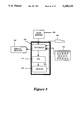
FIG. 3 is a block diagram representation of an exemplary computer system utilized in the preferred embodiment of the present invention.
FIGS. 4a and 4b is a flowchart which illustrate the preferred embodiment of the present invention.
FIGS. 5a-5d respectively illustrate a schematic net list, layout net list and exemplary output, illustrating hierarchical comparison of net lists and components.
FIGS. 6a-6j respectively illustrate a schematic net list, layout net list, and output generated illustrating the hierarchical comparison of net lists having different hierarchies.
NOTATION AND NOMENCLATURE
The detailed descriptions which follow are presented largely in terms of algorithms and symbolic representations of operations on data bits within a computer memory. These algorithmic descriptions and representations are the means used by those skilled in the data processing arts to most effectively convey the substance of their work to others skilled in the art.
An algorithm is here, and generally, conceived to be a self-consistent sequence of steps leading to a desired result. These steps are those requiring physical manipulations of physical quantities. Usually, though not necessarily, these quantities take the form of electrical or magnetic signals capable of being stored, transferred, combined, compared, and otherwise manipulated. It proves convenient at times, principally for reasons of common usage, to refer to these signals as bits, values, elements, symbols, characters, terms, numbers, or the like. It should be borne in mind, however, that all of these and similar terms are to be associated with the appropriate physical quantities and are merely convenient labels applied to these quantities.
Further, the manipulations performed are often referred to in terms, such as adding or comparing, which are commonly associated with mental operations performed by a human operator. No such capability of a human operator is necessary, or desirable in most cases, in any of the operations described herein which form part of the present invention; the operations are machine operations. Useful machines for performing the operations of the present invention include general purpose digital computers or other similar devices. In all cases there should be borne in mind the distinction between the method operations in operating a computer and the method of computation itself. The present invention relates to method steps for operating a computer in processing electrical or other (e.g., mechanical, chemical) physical signals to generate other desired physical signals.
The present invention also relates to apparatus for performing these operations. This apparatus may be specially constructed for the required purposes or it may comprise a general purpose computer as selectively activated or reconfigured by a computer program stored in the computer. The algorithms presented herein are not inherently related to a particular computer or other apparatus. In particular, various general purpose machines may be used with programs written in accordance with the teachings herein, or it may prove more convenient to construct more specialized apparatus to perform the required method steps. The required structure for a variety of these machines will appear from the description given below.
DETAILED DESCRIPTION OF THE INVENTION
General System Configuration
FIG. 3 shows a typical computer-based system for performing hierarchical comparisons of schematic and layout designs according to the present invention. Shown there is a computer 101 which comprises three major components. The first of these is the input/output (I/0) circuit 102 which is used to communicate information in appropriately structured form to and from the other parts of the computer 101. Also shown as a part of computer 101 is the central processing unit (CPU) 103 and memory 104. These latter two elements are those typically found in most general purpose computers and almost all special purpose computers. In fact, the several elements contained within computer 101 are intended to be representative of this broad category of data processors. Particular examples of suitable data processors to fill the role of computer 101 include machines manufactured by Sun Microsystems, Inc., Mountain View, Calif. Other computers having like capabilities may of course be adapted in a straightforward manner to perform the functions described below.
Also shown in FIG. 3 is an input device 105, shown in typical embodiment as a keyboard. It should be understood, however, that the input device may actually be a card reader, magnetic or paper tape reader, or other well-known input device (including, of course, another computer). A mass memory device 106 is coupled to the I/O circuit 102 and provides additional storage capability for the computer 101. The mass memory may include other programs and the like and may take the form of a magnetic or paper tape reader or other well known device. It will be appreciated that the data retained within mass memory 106, may, in appropriate cases, be incorporated in standard fashion into computer 101 as part of memory 104.
In addition, a display monitor 107 is illustrated which is used to display messages or other communications to the user. Such a display monitor may take the form of any of several well-known varieties of CRT displays. A cursor control 108 is used to select command modes and edit the input data, and in general provides a more convenient means to input information into the system.
Process Description
In the process of the present invention, the names of the blocks identified in the net lists are first compared. If the same name exists on the layout and logic net lists, it is initially assumed that the blocks are the same and the block components (blocks and devices) of the block are compared to determine if they are the same. If the elements of the block match, then the blocks are determined to be the same and a correspondence list is generated. This correspondence list has a pair of entry points associated with each terminal or node of the block design. The first entry is the schematic pin position and the second entry is the pin position of the corresponding layout pin. At higher hierarchical levels it is preferred that for each placement of the block it is verified that a matched net goes to the terminals which belong to an entry pair in the correspondence list. Subsequent instantiations of the block are thus compared at the block level without comparing the individual elements of the block each time.
This process begins at the lowest hierarchical level and continues up the hierarchy of blocks until all possible blocks/sub-blocks are matched. For each level of hierarchy, schematic and layout representations are reduced to a common form in terms of placements (instantiations) of lower level matched blocks and devices. These two representations are then compared in terms of blocks and devices.
The process is better illustrated with reference to the flowchart depicted in FIGS. 4a and 4b.
At step 600 a hierarchical net list is extracted from the schematic design and at step 610 a hierarchical net list is extracted from the layout design. The hierarchical net list contains a listing of the blocks and devices which comprise the circuit and the blocks and devices instantiated within each block. At step 615, the various hierarchical elements are sorted in order of hierarchical levels starting with the highest order first. The net lists may be sorted by examining the components within each block and sorting the block containing instantiations of other blocks to be at a higher hierarchical level than the instantiated blocks. Similarly, each block may be identified by a hierarchical level identifier for quick sorting or pre-sorted in hierarchical order.
At step 620, starting with the lowest level the block name in the schematic net list is compared to the block names in the layout net list. If there is no match then that block is marked for flattening, i.e. all instantiations of the block would be flattened in terms of its components (devices and lower level blocks) for verification. A list of blocks for which block names in schematic and layout net list are same is formed and sorted in order of hierarchical levels. Starting from the lowest and block level, set 635, in the common name list, the schematic and the layout representation for the common named block are, at step 637, reduced to a common representation in terms of instantiations of matched (common-named) lower level blocks and devices, flattening all the instantiations of the marked blocks. At step 640 the two canonical representations are compared. A device comparison technique, such as graph isomorphism, is used to perform the device comparison. At step 645, if all devices, instances of lower level blocks and connections match in the two representations then at step 650 a pin correspondence list is generated for the terminals in the schematic representation. The correspondence list contains an identification of pairs, entry points (terminals) from the layout and schematic net lists which correspond to one another. This is done at the node level (i.e., terminals internal and external to the block) to assist the user in identifying errors caused by misconnections of terminals.
The correspondence list is used to simplify subsequent comparisons of instances of this block in blocks at the higher levels of the hierarchy. To verify subsequent instantiations of a verified block, the correspondence list is utilized to compare the entry points of the subsequent instantiations. If the entry point pairs as specified in the correspondence list match, the instantiation of the block is verified without the need to compare each component within the block. At step 655 the process is repeated for the next block in the list until all hierarchical levels have been compared and verified, step 660. A report is then generated, step 670, describing the test results. If the comparison at step 647 fails then the errors are reported for the block. If the error is total such that subsequent comparisons cannot be performed, the process is halted.
An example of a simple test executed according to a preferred embodiment of the present invention is shown in FIGS. 5a-5d. FIG. 5a shows a listing of the net list for the schematic design comprising a block "soai21b" consisting of 2 pfet and 3 nfet devices. The main circuit is identified as fr-- muxlgc consisting of block soai21b at instance 123 having nodes, brad inp1 inp2 d4 d5 d6 d7 inp3 prad and outp drat.
The net list for the layout design is shown in FIG. 5b which also has a block identified as "soai21b" having three pfet and three nfet devices which are instantiated inside main circuit fr-- muxlgc having an instance numbered 123 of component soai21b. Thus when the two circuit net lists are compared as shown in FIGS. 5c-5d, the hierarchical list will consist of block soai21b and block fr-- muxlgc and block soai21b, at the lower hierarchical level will be compared first. As identified in the listing of FIGS. 5c-5d the schematic net list for soai21b (referred to in FIGS. 5c-5d as "network") is reduced to the component device, in the present example, the device level, as in the layout net list, in order to compare the blocks for verification. If block soai21b contained instances of blocks, these blocks would have been previously verified because the blocks would be at a lower hierarchical level and verification of the instances of the blocks within soai21b would be achieved through comparison of the correspondence list. However, if a block within soai21b had been marked as not having corresponding blocks in both the layout and schematic, the block would be flattened and compared on the device level.
Through comparison of terminal names, six corresponding node names are found. In this embodiment, it is initially assumed that the similarly named terminals correspond, but correspondence is checked during "full network trace" for complete verification. during full network trace, the network of components and nodes are compared to determine if the connectivity in the layout and schematic are the same. Each node is examined to determine the devices and/or blocks connected to the node. For each device connected to the node, it is verified that the same type of device (e.g. pfet) is connected in both layout and schematic to the same terminal of the device. This can be determined according to the terminal position in the list of terminals. For the instantiation of the device, the position of the terminal in the list corresponds to a specific terminal in the device.
For example, in FIGS. 5a and 5b, it is verified that pfet instance 4 "4 pfet" has the first terminal (4.D) connected to the same node. Although the first terminal in the present illustration is identified by the same name in the layout and schematic, it is possible terminals to be identified by different names and will be identified as such in the correspondence list.
Similarly, instances of previously verified blocks are verified by comparing the block names and the nodes as specified by the correspondence list. If nodes of the present instance of the block do not equal the nodes in the correspondence list, an error is noted.
After the networks are verified, the device sizes are compared to determine if the sizes of corresponding devices in the schematic and layout match. This is determined by comparing the sizes specified in the net list, e.g. "w 16 1.8" for pfet instance 4 in FIG. 5a. If the device sizes do not match an error is generated. If the sizes match the system will report "sub ckts match", indicating that the blocks match (i.e., "clean") and the correspondence list is generated. Once block soai27b is verified, the block is identified as being "clean." and the next hierarchy level is then compared. In the present illustration it is the highest level although it should be evident that this process applies to a multi-hierarchy type system having a large number of levels. The circuit fr-- muxlgc is then compared to the circuit in the layout design. The same verification process is performed, fr-- muxlgc is found to have four nodes, inp1, inp2 outp which correspond to layout node inp1, inp2, inp3 and outp in the layout design identifying that the comparison is clean and the designs match.
FIGS. 6a-6j illustrate a second comparison between a schematic FIGS. 6a-6d and layout FIGS. 6e-6g in which the hierarchies do not precisely match and therefore some of the elements or sub-circuits must be flattened out to the component level for the comparison. For example, referring to FIGS. 6a-6d, the schematic design comprises a circuit syncce114 consisting of elements sync-- ce114, nand2, sor02d, sin00d, san02d and the layout design (FIGS. 6e-6g ) comprises a circuit syncce114 consisting of the elements sin00d, snd02c, snr02c and a number of nfets and pfets. Close examination of the description for syncce114 in the schematic and the layout design indicates that the hierarchical structures in the designs are not the same. However, that does not mean that the net lists do not match when flattened to at the component level. Referring to FIGS. 6h-6j, sub-circuit snr02c in the schematic is compared to the sub-circuit snr02c in the layout and are found to match. In addition, the sub-circuits sin00d and snd02c in the layout design are compared to sub-arrays sin00d and snd02c respectively in the schematic design. However, the remaining sub-circuits, for example, the nfets and pfets individually listed in the layout design, FIGS. 6e-6g, and the sub-circuits sync-- ce114 nand2, sor02d and san02d in the schematic design, FIGS. 6a-6d, are not found to have corresponding sub-circuits. The schematic representation of syncce114 is reduced to a representation in terms of sin00d, sn02c, snd02c and devices nfet and pfet. Instantiations of syn-- ce114, nand2 are flattened. The layout representation is also transformed into a representation in terms of sin00d, sn02c, snd02c and devices nfet and pfet. These two transformed representations are then compared to verify the validity of the layout design.
While the invention has been described in conjunction with the preferred embodiment, it is evident that numerous alternatives, modifications, variations and uses will be apparent to those skilled in the art in light of the foregoing description.