US5250758A - Methods and systems of preparing extended length flexible harnesses - Google Patents
Methods and systems of preparing extended length flexible harnesses Download PDFInfo
- Publication number
- US5250758A US5250758A US07/703,724 US70372491A US5250758A US 5250758 A US5250758 A US 5250758A US 70372491 A US70372491 A US 70372491A US 5250758 A US5250758 A US 5250758A
- Authority
- US
- United States
- Prior art keywords
- substrate
- extended length
- harness according
- length printed
- harness
- Prior art date
- Legal status (The legal status is an assumption and is not a legal conclusion. Google has not performed a legal analysis and makes no representation as to the accuracy of the status listed.)
- Expired - Fee Related
Links
Images


Classifications
-
- H—ELECTRICITY
- H02—GENERATION; CONVERSION OR DISTRIBUTION OF ELECTRIC POWER
- H02G—INSTALLATION OF ELECTRIC CABLES OR LINES, OR OF COMBINED OPTICAL AND ELECTRIC CABLES OR LINES
- H02G3/00—Installations of electric cables or lines or protective tubing therefor in or on buildings, equivalent structures or vehicles
-
- H—ELECTRICITY
- H01—ELECTRIC ELEMENTS
- H01K—ELECTRIC INCANDESCENT LAMPS
- H01K1/00—Details
-
- H—ELECTRICITY
- H05—ELECTRIC TECHNIQUES NOT OTHERWISE PROVIDED FOR
- H05K—PRINTED CIRCUITS; CASINGS OR CONSTRUCTIONAL DETAILS OF ELECTRIC APPARATUS; MANUFACTURE OF ASSEMBLAGES OF ELECTRICAL COMPONENTS
- H05K3/00—Apparatus or processes for manufacturing printed circuits
- H05K3/02—Apparatus or processes for manufacturing printed circuits in which the conductive material is applied to the surface of the insulating support and is thereafter removed from such areas of the surface which are not intended for current conducting or shielding
- H05K3/04—Apparatus or processes for manufacturing printed circuits in which the conductive material is applied to the surface of the insulating support and is thereafter removed from such areas of the surface which are not intended for current conducting or shielding the conductive material being removed mechanically, e.g. by punching
- H05K3/046—Apparatus or processes for manufacturing printed circuits in which the conductive material is applied to the surface of the insulating support and is thereafter removed from such areas of the surface which are not intended for current conducting or shielding the conductive material being removed mechanically, e.g. by punching by selective transfer or selective detachment of a conductive layer
-
- H—ELECTRICITY
- H05—ELECTRIC TECHNIQUES NOT OTHERWISE PROVIDED FOR
- H05K—PRINTED CIRCUITS; CASINGS OR CONSTRUCTIONAL DETAILS OF ELECTRIC APPARATUS; MANUFACTURE OF ASSEMBLAGES OF ELECTRICAL COMPONENTS
- H05K3/00—Apparatus or processes for manufacturing printed circuits
- H05K3/02—Apparatus or processes for manufacturing printed circuits in which the conductive material is applied to the surface of the insulating support and is thereafter removed from such areas of the surface which are not intended for current conducting or shielding
- H05K3/06—Apparatus or processes for manufacturing printed circuits in which the conductive material is applied to the surface of the insulating support and is thereafter removed from such areas of the surface which are not intended for current conducting or shielding the conductive material being removed chemically or electrolytically, e.g. by photo-etch process
- H05K3/061—Etching masks
- H05K3/065—Etching masks applied by electrographic, electrophotographic or magnetographic methods
-
- H—ELECTRICITY
- H05—ELECTRIC TECHNIQUES NOT OTHERWISE PROVIDED FOR
- H05K—PRINTED CIRCUITS; CASINGS OR CONSTRUCTIONAL DETAILS OF ELECTRIC APPARATUS; MANUFACTURE OF ASSEMBLAGES OF ELECTRICAL COMPONENTS
- H05K3/00—Apparatus or processes for manufacturing printed circuits
- H05K3/10—Apparatus or processes for manufacturing printed circuits in which conductive material is applied to the insulating support in such a manner as to form the desired conductive pattern
- H05K3/102—Apparatus or processes for manufacturing printed circuits in which conductive material is applied to the insulating support in such a manner as to form the desired conductive pattern by bonding of conductive powder, i.e. metallic powder
-
- H—ELECTRICITY
- H05—ELECTRIC TECHNIQUES NOT OTHERWISE PROVIDED FOR
- H05K—PRINTED CIRCUITS; CASINGS OR CONSTRUCTIONAL DETAILS OF ELECTRIC APPARATUS; MANUFACTURE OF ASSEMBLAGES OF ELECTRICAL COMPONENTS
- H05K3/00—Apparatus or processes for manufacturing printed circuits
- H05K3/10—Apparatus or processes for manufacturing printed circuits in which conductive material is applied to the insulating support in such a manner as to form the desired conductive pattern
- H05K3/12—Apparatus or processes for manufacturing printed circuits in which conductive material is applied to the insulating support in such a manner as to form the desired conductive pattern using thick film techniques, e.g. printing techniques to apply the conductive material or similar techniques for applying conductive paste or ink patterns
- H05K3/1241—Apparatus or processes for manufacturing printed circuits in which conductive material is applied to the insulating support in such a manner as to form the desired conductive pattern using thick film techniques, e.g. printing techniques to apply the conductive material or similar techniques for applying conductive paste or ink patterns by ink-jet printing or drawing by dispensing
- H05K3/125—Apparatus or processes for manufacturing printed circuits in which conductive material is applied to the insulating support in such a manner as to form the desired conductive pattern using thick film techniques, e.g. printing techniques to apply the conductive material or similar techniques for applying conductive paste or ink patterns by ink-jet printing or drawing by dispensing by ink-jet printing
-
- H—ELECTRICITY
- H05—ELECTRIC TECHNIQUES NOT OTHERWISE PROVIDED FOR
- H05K—PRINTED CIRCUITS; CASINGS OR CONSTRUCTIONAL DETAILS OF ELECTRIC APPARATUS; MANUFACTURE OF ASSEMBLAGES OF ELECTRICAL COMPONENTS
- H05K3/00—Apparatus or processes for manufacturing printed circuits
- H05K3/10—Apparatus or processes for manufacturing printed circuits in which conductive material is applied to the insulating support in such a manner as to form the desired conductive pattern
- H05K3/12—Apparatus or processes for manufacturing printed circuits in which conductive material is applied to the insulating support in such a manner as to form the desired conductive pattern using thick film techniques, e.g. printing techniques to apply the conductive material or similar techniques for applying conductive paste or ink patterns
- H05K3/1266—Apparatus or processes for manufacturing printed circuits in which conductive material is applied to the insulating support in such a manner as to form the desired conductive pattern using thick film techniques, e.g. printing techniques to apply the conductive material or similar techniques for applying conductive paste or ink patterns by electrographic or magnetographic printing
-
- H—ELECTRICITY
- H05—ELECTRIC TECHNIQUES NOT OTHERWISE PROVIDED FOR
- H05K—PRINTED CIRCUITS; CASINGS OR CONSTRUCTIONAL DETAILS OF ELECTRIC APPARATUS; MANUFACTURE OF ASSEMBLAGES OF ELECTRICAL COMPONENTS
- H05K3/00—Apparatus or processes for manufacturing printed circuits
- H05K3/10—Apparatus or processes for manufacturing printed circuits in which conductive material is applied to the insulating support in such a manner as to form the desired conductive pattern
- H05K3/18—Apparatus or processes for manufacturing printed circuits in which conductive material is applied to the insulating support in such a manner as to form the desired conductive pattern using precipitation techniques to apply the conductive material
- H05K3/181—Apparatus or processes for manufacturing printed circuits in which conductive material is applied to the insulating support in such a manner as to form the desired conductive pattern using precipitation techniques to apply the conductive material by electroless plating
- H05K3/182—Apparatus or processes for manufacturing printed circuits in which conductive material is applied to the insulating support in such a manner as to form the desired conductive pattern using precipitation techniques to apply the conductive material by electroless plating characterised by the patterning method
-
- G—PHYSICS
- G03—PHOTOGRAPHY; CINEMATOGRAPHY; ANALOGOUS TECHNIQUES USING WAVES OTHER THAN OPTICAL WAVES; ELECTROGRAPHY; HOLOGRAPHY
- G03G—ELECTROGRAPHY; ELECTROPHOTOGRAPHY; MAGNETOGRAPHY
- G03G15/00—Apparatus for electrographic processes using a charge pattern
- G03G15/22—Apparatus for electrographic processes using a charge pattern involving the combination of more than one step according to groups G03G13/02 - G03G13/20
- G03G15/225—Apparatus for electrographic processes using a charge pattern involving the combination of more than one step according to groups G03G13/02 - G03G13/20 using contact-printing
-
- H—ELECTRICITY
- H05—ELECTRIC TECHNIQUES NOT OTHERWISE PROVIDED FOR
- H05K—PRINTED CIRCUITS; CASINGS OR CONSTRUCTIONAL DETAILS OF ELECTRIC APPARATUS; MANUFACTURE OF ASSEMBLAGES OF ELECTRICAL COMPONENTS
- H05K1/00—Printed circuits
- H05K1/02—Details
- H05K1/03—Use of materials for the substrate
- H05K1/0393—Flexible materials
-
- H—ELECTRICITY
- H05—ELECTRIC TECHNIQUES NOT OTHERWISE PROVIDED FOR
- H05K—PRINTED CIRCUITS; CASINGS OR CONSTRUCTIONAL DETAILS OF ELECTRIC APPARATUS; MANUFACTURE OF ASSEMBLAGES OF ELECTRICAL COMPONENTS
- H05K1/00—Printed circuits
- H05K1/02—Details
- H05K1/11—Printed elements for providing electric connections to or between printed circuits
- H05K1/118—Printed elements for providing electric connections to or between printed circuits specially for flexible printed circuits, e.g. using folded portions
-
- H—ELECTRICITY
- H05—ELECTRIC TECHNIQUES NOT OTHERWISE PROVIDED FOR
- H05K—PRINTED CIRCUITS; CASINGS OR CONSTRUCTIONAL DETAILS OF ELECTRIC APPARATUS; MANUFACTURE OF ASSEMBLAGES OF ELECTRICAL COMPONENTS
- H05K1/00—Printed circuits
- H05K1/16—Printed circuits incorporating printed electric components, e.g. printed resistor, capacitor, inductor
-
- H—ELECTRICITY
- H05—ELECTRIC TECHNIQUES NOT OTHERWISE PROVIDED FOR
- H05K—PRINTED CIRCUITS; CASINGS OR CONSTRUCTIONAL DETAILS OF ELECTRIC APPARATUS; MANUFACTURE OF ASSEMBLAGES OF ELECTRICAL COMPONENTS
- H05K2203/00—Indexing scheme relating to apparatus or processes for manufacturing printed circuits covered by H05K3/00
- H05K2203/01—Tools for processing; Objects used during processing
- H05K2203/0104—Tools for processing; Objects used during processing for patterning or coating
- H05K2203/013—Inkjet printing, e.g. for printing insulating material or resist
-
- H—ELECTRICITY
- H05—ELECTRIC TECHNIQUES NOT OTHERWISE PROVIDED FOR
- H05K—PRINTED CIRCUITS; CASINGS OR CONSTRUCTIONAL DETAILS OF ELECTRIC APPARATUS; MANUFACTURE OF ASSEMBLAGES OF ELECTRICAL COMPONENTS
- H05K2203/00—Indexing scheme relating to apparatus or processes for manufacturing printed circuits covered by H05K3/00
- H05K2203/05—Patterning and lithography; Masks; Details of resist
- H05K2203/0502—Patterning and lithography
- H05K2203/0517—Electrographic patterning
-
- H—ELECTRICITY
- H05—ELECTRIC TECHNIQUES NOT OTHERWISE PROVIDED FOR
- H05K—PRINTED CIRCUITS; CASINGS OR CONSTRUCTIONAL DETAILS OF ELECTRIC APPARATUS; MANUFACTURE OF ASSEMBLAGES OF ELECTRICAL COMPONENTS
- H05K2203/00—Indexing scheme relating to apparatus or processes for manufacturing printed circuits covered by H05K3/00
- H05K2203/05—Patterning and lithography; Masks; Details of resist
- H05K2203/0502—Patterning and lithography
- H05K2203/0522—Using an adhesive pattern
-
- H—ELECTRICITY
- H05—ELECTRIC TECHNIQUES NOT OTHERWISE PROVIDED FOR
- H05K—PRINTED CIRCUITS; CASINGS OR CONSTRUCTIONAL DETAILS OF ELECTRIC APPARATUS; MANUFACTURE OF ASSEMBLAGES OF ELECTRICAL COMPONENTS
- H05K2203/00—Indexing scheme relating to apparatus or processes for manufacturing printed circuits covered by H05K3/00
- H05K2203/05—Patterning and lithography; Masks; Details of resist
- H05K2203/0502—Patterning and lithography
- H05K2203/0528—Patterning during transfer, i.e. without preformed pattern, e.g. by using a die, a programmed tool or a laser
-
- H—ELECTRICITY
- H05—ELECTRIC TECHNIQUES NOT OTHERWISE PROVIDED FOR
- H05K—PRINTED CIRCUITS; CASINGS OR CONSTRUCTIONAL DETAILS OF ELECTRIC APPARATUS; MANUFACTURE OF ASSEMBLAGES OF ELECTRICAL COMPONENTS
- H05K2203/00—Indexing scheme relating to apparatus or processes for manufacturing printed circuits covered by H05K3/00
- H05K2203/07—Treatments involving liquids, e.g. plating, rinsing
- H05K2203/0703—Plating
- H05K2203/0709—Catalytic ink or adhesive for electroless plating
-
- H—ELECTRICITY
- H05—ELECTRIC TECHNIQUES NOT OTHERWISE PROVIDED FOR
- H05K—PRINTED CIRCUITS; CASINGS OR CONSTRUCTIONAL DETAILS OF ELECTRIC APPARATUS; MANUFACTURE OF ASSEMBLAGES OF ELECTRICAL COMPONENTS
- H05K2203/00—Indexing scheme relating to apparatus or processes for manufacturing printed circuits covered by H05K3/00
- H05K2203/10—Using electric, magnetic and electromagnetic fields; Using laser light
- H05K2203/107—Using laser light
-
- H—ELECTRICITY
- H05—ELECTRIC TECHNIQUES NOT OTHERWISE PROVIDED FOR
- H05K—PRINTED CIRCUITS; CASINGS OR CONSTRUCTIONAL DETAILS OF ELECTRIC APPARATUS; MANUFACTURE OF ASSEMBLAGES OF ELECTRICAL COMPONENTS
- H05K2203/00—Indexing scheme relating to apparatus or processes for manufacturing printed circuits covered by H05K3/00
- H05K2203/15—Position of the PCB during processing
- H05K2203/1545—Continuous processing, i.e. involving rolls moving a band-like or solid carrier along a continuous production path
-
- H—ELECTRICITY
- H05—ELECTRIC TECHNIQUES NOT OTHERWISE PROVIDED FOR
- H05K—PRINTED CIRCUITS; CASINGS OR CONSTRUCTIONAL DETAILS OF ELECTRIC APPARATUS; MANUFACTURE OF ASSEMBLAGES OF ELECTRICAL COMPONENTS
- H05K3/00—Apparatus or processes for manufacturing printed circuits
- H05K3/10—Apparatus or processes for manufacturing printed circuits in which conductive material is applied to the insulating support in such a manner as to form the desired conductive pattern
- H05K3/18—Apparatus or processes for manufacturing printed circuits in which conductive material is applied to the insulating support in such a manner as to form the desired conductive pattern using precipitation techniques to apply the conductive material
- H05K3/181—Apparatus or processes for manufacturing printed circuits in which conductive material is applied to the insulating support in such a manner as to form the desired conductive pattern using precipitation techniques to apply the conductive material by electroless plating
- H05K3/182—Apparatus or processes for manufacturing printed circuits in which conductive material is applied to the insulating support in such a manner as to form the desired conductive pattern using precipitation techniques to apply the conductive material by electroless plating characterised by the patterning method
- H05K3/185—Apparatus or processes for manufacturing printed circuits in which conductive material is applied to the insulating support in such a manner as to form the desired conductive pattern using precipitation techniques to apply the conductive material by electroless plating characterised by the patterning method by making a catalytic pattern by photo-imaging
-
- H—ELECTRICITY
- H05—ELECTRIC TECHNIQUES NOT OTHERWISE PROVIDED FOR
- H05K—PRINTED CIRCUITS; CASINGS OR CONSTRUCTIONAL DETAILS OF ELECTRIC APPARATUS; MANUFACTURE OF ASSEMBLAGES OF ELECTRICAL COMPONENTS
- H05K3/00—Apparatus or processes for manufacturing printed circuits
- H05K3/22—Secondary treatment of printed circuits
- H05K3/28—Applying non-metallic protective coatings
- H05K3/281—Applying non-metallic protective coatings by means of a preformed insulating foil
-
- Y—GENERAL TAGGING OF NEW TECHNOLOGICAL DEVELOPMENTS; GENERAL TAGGING OF CROSS-SECTIONAL TECHNOLOGIES SPANNING OVER SEVERAL SECTIONS OF THE IPC; TECHNICAL SUBJECTS COVERED BY FORMER USPC CROSS-REFERENCE ART COLLECTIONS [XRACs] AND DIGESTS
- Y10—TECHNICAL SUBJECTS COVERED BY FORMER USPC
- Y10S—TECHNICAL SUBJECTS COVERED BY FORMER USPC CROSS-REFERENCE ART COLLECTIONS [XRACs] AND DIGESTS
- Y10S428/00—Stock material or miscellaneous articles
- Y10S428/901—Printed circuit
Definitions
- the present invention relates generally to systems and methods for designing and fabricating conductive wiring harnesses. More particularly, the invention relates to methods for fabricating wiring harnesses as uninterrupted (i.e., seamless) flexible printed circuitry of unlimited dimension on a continuous, web-fed substrate.
- RWHs round wire harnesses
- An RWH typically includes a bundle of individual wire conductors terminated in connectors for attachment to the various circuit components.
- RWH provides large scale interconnection of components, it suffers from significant drawbacks. For example, because RWH is used in large scale systems, the number of conductive paths is relatively large. The complex routing and connection of the various conductive paths therefore make it difficult to handle the RWH and render assembly of a system using RWH labor intensive. Use of an RWH also results in a highly disorganized wiring scheme in which misconnections of conductors frequently occur and in which location of faults (e.g., breaks in conductive paths) cannot be readily identified and corrected.
- RWH includes a large number of individual, round conductors which consume a significant volume of space and which add substantial weight to a system. Because individual wires are routed, an RWH is also highly susceptible to cross-talk and to impedance mismatches with system components.
- an RWH is a bundle of individual wire conductors
- the strength of the overall system is limited to the strength of each individual conductor. Therefore, if a single wire is structurally stressed (i.e., typically the shortest conductor), that conductor can break. As mentioned previously, subsequent identification and correction of such breaks are difficult due to the routing complexity of an RWH. Further, this structural limitation often leads to a harness configuration being dictated by strength requirements rather than electrical requirements, such that the harness is often heavier than necessary.
- an FPW circuit layout is designed by first creating a circuit layout master. Using the circuit layout master, a layout of conductors is imaged on a photographic negative from which a camera positive is produced. A screen is then fabricated from the camera positive for applying resist to the copper surface of a base material (i.e., substrate).
- a base material i.e., substrate
- etching is used to remove copper left unprotected by the resist.
- the remaining copper constitutes a desired pattern of conductive paths on the substrate.
- an insulating overlay is subsequently laminated to the surface, the overlay being of the same material as the base.
- the camera negative is used to form the layout of conductive paths.
- a photoresist is applied to the entire copper surface.
- ultraviolet light is passed through the camera negative to "fix" the photoresist material to the base in those areas where conductive paths are to be formed.
- Unprotected areas of the copper layer are then chemically etched, followed by lamination with an insulating overlay, as described above.
- U.S. Pat. No. 4,587,719 discloses a method of batch fabricating flexible circuits in an effort to provide area efficient use of a size limited substrate. As disclosed therein, orthoganol lines of conductors are joined and folded about axes parallel to the conductors. Although the disclosed method permits flexible arrays to be fabricated, its use of traditional imaging techniques imposes size constraints on the overall circuit layout design which prohibit its use as an RWH.
- U.S. Pat. No. 3,819,989 relates to a printed wiring multiple circuit board assembly wherein printed circuit boards are arranged at right angles to a flexible main tape 10.
- the flexible main tape is formed with a plurality of conductors and tape tabs 12 through 15 using conventional techniques.
- the tape tabs connect the main tape 10 and a plurality of overlays 16 through 19.
- the overlays are formed on each side of the main tape and are bonded to conventional rectangular circuit boards situated in mutually parallel planes perpendicular to the main tape.
- the system of U.S. Pat. No. 3,819,989 fails to disclose fabrication techniques which would permit the manufacture of RWH replacements.
- U.S. Pat. No. 3,712,735 discloses a photoresist pattern controlled continuous strip etching apparatus.
- a continuous loop photographic film transparency of a master pattern is used for contact photo printing of the pattern onto a moving resist coated strip.
- this apparatus merely addresses the problems associated with step and repeat processes by increasing the size of the master film transparency, many of the aforementioned drawbacks associated with small scale FPW applications are incurred.
- circuits produced by the disclosed apparatus are limited to the size of the master film transparency and are not readily adapted to in-line modifications of the conductor patterns once the master film transparency has been produced.
- a purpose of the present invention is to provide systems and methods for fabricating electrical harnesses capable of replacing RWH.
- the harness should provide three-dimensional breakout routing capability and be free of size restrictions.
- a purpose of the invention is to provide systems and methods for fabricating harnesses such that the circuit layout can be readily modified electronically with limited manipulation of the fabrication process. Such design modifications include, for example, adaptation of a given circuit layout to systems of varied shapes and dimensions.
- a purpose of the invention is to provide high throughput of a harness from design to manufacture, and to eliminate high cost inventory requirements associated with the manufacture of traditional RWH.
- an in-line raster scanning (e.g., xerography or laser printing) is used to image conductor patterns on a continuous, web-fed base material, or substrate. As the substrate is fed, the raster scanned image is continuously refreshed.
- an uninterrupted (i.e, seamless) FPW harness equivalent to a discrete RWH of unlimited size in three dimensions can be fabricated.
- the substrate can be cut to form circuit layout branches which are subsequently folded to produce three-dimensional shapes of unlimited size.
- a harness fabricated in accordance with the present invention represents an organized layout of conductive paths having relatively small volume and weight requirements and enabling excellent control of cross-talk and impedance mismatches.
- the present invention affords significant advantages not previously realized in fabricating harnesses of any size.
- the in-line raster scanning of a conductor pattern onto a continuously fed substrate provides high throughput while affording optimum design flexibility.
- An original FPW design and/or subsequent design modifications can be remotely communicated via, for example, telephone networks.
- Virtual inventory or electronic inventory can also be exploited in preferred embodiments to avoid any need to maintain a supply of round wire conductors having different sizes and color codes. Only generic raw materials need be maintained in inventory. Because various conductive paths of the layout can be labelled during fabrication, any need to label round wires (traditionally done by direct printing on the wire jacket, color coding or the addition of label sleeves) can be eliminated.
- Yet another advantage of the present invention is that the fabrication of a harness as a single FPW element relieves the strain placed on the individual conductors of an RWH. Further, the ability to contour FPW to irregularly shaped surfaces in accordance with the present invention permits increased heat sinking.
- an extended length flexible printed electrical harness is created by continuously feeding a substrate to an imaging means.
- an image of a continuously updated conductor pattern is created electronically on a computer or in hard copy such that the image can be transferred to the substrate.
- the substrate is raster scanned either directly or indirectly to image the conductor pattern thereon.
- Conductive paths are established on the substrate in accordance with the pattern and are covered with a protective insulating film.
- the flexible substrate is then cut to form circuit layout breakouts, or branches, and the branches are folded to produce three-dimensional shapes of unlimited size.
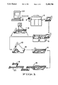
- FIG. 1 shows an exemplary system for fabricating an FPW harness in accordance with a preferred embodiment
- FIG. 2 shows an exemplary, uncut FPW harness formed in accordance with a preferred embodiment
- FIG. 3 shows a more detailed illustration of an exemplary FPW harness formed, cut and folded in accordance with a preferred embodiment
- FIG. 4 shows an exemplary FPW harness formed, cut, folded and placed for a given end use.
- an extended length FPW harness of conductive paths is fabricated by continuously moving, or web-feeding, an uninterrupted (i.e., seamless) flexible substrate through four general fabrication stations.
- the first of these includes an imaging means wherein an image of a continuously updated conductor pattern is created electronically on a computer or in hard copy such that the image can be transferred to the substrate.
- the substrate is raster scanned either directly or indirectly to image the conductor pattern on the substrate as it is fed.
- conductive paths are established on the substrate in accordance with the pattern.
- the conductive paths are subsequently covered with a protective insulating film in a third general stage.
- the flexible substrate passes to a fourth general stage wherein it is cut to form circuit layout breakouts, or branches. The branches can then be folded to produce three-dimensional shapes.
- four general techniques can be used for creating conductive paths on the web-fed substrate: an additive process of forming conductive paths; a subtractive process of forming conductive paths; a conductive ink process; and a tack and peel process.
- the technique selected for creating the conductive paths will dictate the technique or techniques which can be used to image the conductor pattern, either directly or indirectly, on the substrate. Accordingly, a brief discussion of the four general techniques for creating conductive paths will be provided before discussing the various imaging techniques.
- raster scanning is used to image a conductor pattern corresponding to the paths of an RWH. Further, patterns can be raster scanned on the substrate for in-line testing and inspection of circuits. Raster scanning can be effected in a manner similar to that described in the book Imaging Processes and Materials. Sturge, J. M. et al., 8th ed., 1989, the disclosure of which is hereby incorporated by reference in its entirety. For example, Chapter 13 of the aforementioned book is entitled “Non-Impact Printing Technologies" by Werner E. Haas and describes raster scanning with a scanning e-beam tool on page 377. Further, Chapter 18 of the aforementioned book is entitled “Imaging For Microfabrication", by J. M. Shaw and describes the use of deflectors for raster scanning on page 578.
- raster scanning generally refers to mechanical and electrical scanning with, for example, an electron beam.
- the beam is switched on and off in accordance with pattern data to image the pattern on a desired surface.
- the substrate is raster scanned, either directly or indirectly, to selectively image a conductor pattern (e.g., transfer plateable toner) on those portions of the substrate where conductive paths are to be formed.
- a conductor pattern e.g., transfer plateable toner
- the patterns are built up (e.g., plated) additively with a conductive material to form the conductive paths.
- the second general technique mentioned was a subtractive process, wherein the substrate is coated in its entirety with a conductive material. Afterwards, the substrate is raster scanned, either directly or indirectly, to image for removal those portions of the substrate where the conductive material is to be removed (positive working resist) or, conversely, to image for retention those portions where the conductive material is to remain (negative working resist).
- an ink-jet printer scans the substrate and deposits a catalytic ink (e.g., containing a binder and catalyst such as Sn/Pd) onto selected portions of the substrate surface.
- a catalytic ink e.g., containing a binder and catalyst such as Sn/Pd
- conductive paths can subsequently be formed on these portions of the substrate using a plating process.
- the imaging of a conductor pattern and the establishment of conductive paths on the pattern can be combined into a single stage.
- an ink-jet printer can be used to directly scan the substrate while depositing ink containing metal spheres or conductive polymers.
- a tacky surface pattern corresponding to a predetermined conductive path is created on the substrate by, for example, transferring electrophotographic or magnetographic toner from a drum, or by ink-jet or dot matrix printing of an adhesive onto the substrate.
- the image of a conductor pattern can be scanned onto a surface coating of the substrate, and the substrate rendered tacky in locally softened imaged areas by light exposure or by chemical or thermal means.
- the surface is subsequently laminated with a metal film. The metal film is then removed (e.g., sucked or peeled) where no tack is available. If the film is very thin, an electrolytic plating step, as will be described below, may be necessary to build up the conductive paths.
- the substrate can be raster scanned either directly or indirectly.
- direct raster scanning encompasses image creation of a conductor pattern directly on the substrate.
- indirect raster scanning encompasses image creation of a conductor pattern on a drum (e.g., photocopier drum) or photosensitive belt. The image is then transferred to the substrate from the drum or belt.
- the image of the conductor pattern is continuously refreshed, or updated, as the substrate is fed.
- a subsequent conductor pattern stored in memory can be prepared for imaging a down line portion of the substrate.
- Direct scanning can be effected using impact or non-impact write-heads, such as: a laser in a laser printer, a nozzle in an ink-jet printer, LEDs, electrophotography (i.e., electrophotographic plateable toner technology), magnetographic plateable toner technology, and ionography (i.e., ionographic plateable toner technology).
- the scanning of the substrate can be effected by deflecting light (e.g., laser light) off a mirror surface or by directing light, liquid or solid particles toward the surface through a pivoting head and a shutter.
- An electrically charged scanning stylus can also be used to electrically erode the substrate to implement a subtractive process.
- the stylus can be any known stylus suitable for piercing, drilling, routing or cutting a surface of the substrate. Any of these direct transfer mechanisms can be situated in clusters or arrays to improve printing speed.
- the aforementioned nozzles can also be known nozzles for transferring a catalytic ink to form a catalytic pattern on the substrate.
- the pattern of catalytic ink is subsequently plated additively to build up conductive paths on the substrate.
- an ink acting as an etch resist can be transferred to the substrate for subsequent etching.
- resist can be selectively fixed on the substrate over those areas where conductive paths of the circuit layout are to be formed.
- Indirect scanning can be effected by transferring a conductor pattern to be formed on the substrate onto a drum as in conventional photocopying (e.g., electrophotography) using liquid toners or dry toners. Subsequently the pattern on the drum is transferred to the substrate. The pattern on the drum is then continuously refreshed, or updated, as the substrate is fed.
- conventional photocopying e.g., electrophotography
- liquid toners or dry toners e.g., electrophotography
- FIG. 1 shows an exemplary in-line system for fabricating extended length FPW harnesses of unlimited dimension on a continuous, web-fed substrate using an additive process.
- a continuous polymer (e.g., polyimide) substrate 2 formed as a flat sheet is web-fed into an imaging means.
- the imaging means is a known laser printer 4, such as a Versatec 8836-II monochrome laser plotter.
- thermoset films such as polyimide films coated with acrylic, epoxy or TFE adhesives, thermoplastic films such as polyester coated with polyester or epoxy adhesives, or polyetherimide (UltemTM) films whose surface acts as an adhesive can be used upon which conductive (e.g., metal) paths can be formed.
- a catalytic plateable toner such as that described in U.S. Pat. No. 4,504,529, is raster scanned directly on the substrate for subsequent electroless plating.
- the use of raster scanning to transfer the catalytic toner onto the continuously moving substrate 2 permits creation of a flexible printed harness having unlimited dimensions.
- the laser printer 4 includes a computer work station 22 which provides in-line computer aided design (CAD) of the conductor pattern on the substrate.
- CAD computer aided design
- original circuit pattern designs and/or modifications can also be received on-line from remote sources (e.g., via telephone networks) and used to update the circuit pattern being imaged (e.g., add or delete patterns).
- CAD can be implemented in a manner similar to that described for conventional printed circuit boards (PCBs) in the article “New Technology Allows Through-Hole and SMT Multilayer Quick Turn Prototype PCBs," PCNetwork, by Bill Schillhamer, December 1990, and U.S. Pat. No. 4,767,489, the disclosures of which are hereby incorporated by reference in their entirety.
- CAD systems such as the Mentor Graphics Cable StationTM can be used to design RWH in three dimensions and to print these harnesses by the techniques described herein on the substrate.
- circuit design modifications can be readily implemented during fabrication.
- irregular images of multiple different circuits can be printed on the same substrate. These irregular images can be nested in a CAD memory before actual printing. By organizing the irregular shapes on the substrate, space usage of the substrate can be optimized and material waste can be minimized upon forming the conductor patterns to a final shape.
- vias through the substrate can be formed to permit interconnection of these patterns. More particularly, prior to imaging a conductor pattern on the substrate, the substrate is perforated to form the vias.
- perforation of the substrate is performed by the imaging means.
- hole punching, cutting, drilling or routing can be effected by:
- Scanning laser ablation e.g., CO 2 or Eximer
- a modified impact or dot matrix printer can be used to directly punch through the substrate layer, or high temperature rods can be used to melt through the substrate.
- the nozzles described previously for scanning the substrate can also be used to effect the aforementioned step of perforating the substrate.
- the nozzles can dispense chemicals for etching the substrate to form the holes (i.e., perforate the substrate) and to carry out routing.
- the nozzles can dispense eroding particles to perform the etching by boring and routing the substrate in a manner akin to sand-blasting.
- the nozzles can direct water toward the substrate for water-jet cutting.
- FIG. 1 depicts an exemplary preferred embodiment
- a totally catalytic substrate surface can be formed either by coating the surface with the catalyst or by incorporation of the catalyst into the substrate material.
- a plating resist can be selectively scanned onto the surface with an imaging means such as a photocopier, a laser printer, an LED/ionographic device, or an ink-jet printer.
- the resist coated portions of the substrate are thus prevented from subsequent plating with conductive materials.
- "ink"-tape on a normal dot matrix printer can be either a catalyst (for electroless plating) or a resist, depending on whether a non-catalytic or a catalytic substrate is used.
- the substrate is coated with a thin metal laminate, and a resist is transferred thereto (e.g., impact or non-impact printing) during the imaging stage.
- the resist is then removed from selected portions of the substrate to image a conductor pattern on the substrate which is subsequently plated to form the conductive paths. Afterwards, removal of the resist and chemical removal of the remaining thin areas which were covered by the resist can be effected.
- different toners e.g., electrophotographic and magnetographic toners
- the catalytic ink in an ink-jet printer can be transferred to form a resist pattern on a metal drum.
- the drum is then additively or electrolytically plated in areas where no resist is present.
- the conductive paths are peeled off the drum by using a substrate which has been coated with a tacky surface.
- subtractive techniques can also be used.
- Subtractive techniques start out with a substrate clad produced by lamination of the polymer substrate with metal films.
- the polymer film may have the metal (e.g., copper) laminated to one or two sides
- An exemplary subtractive method selectively deposits etch resist over areas that are to remain as circuitry. These areas correspond to the conductor patterns which become conductive paths by, for example, chemically etching away the metal left unprotected in the image-producing step.
- An ink-jet printer or dot matrix printer can also be modified to raster scan a substrate and to selectively deposit the etch resist as an ink directly on the substrate.
- toner can be used as a screen on top of a normal etch resist film to effect a subtractive technique for creating an FPW harness.
- Subsequent development of an image representing a conductor pattern of the FPW harness can then be used to produce an etch pattern made from common resist films.
- a high powered laser can be used to remove the etch resist film down to the conductive layer. This exposes those portions of the conductive layer which are to be removed. Plasma etching techniques can also be used to remove the resist film.
- a master can be continuously formed on a transparent surface by, for example, laser printing or ink-jet printing. This master is then synchronously fed into an exposure unit to transfer the conductor pattern image from the transparent film to the photographic etch resist on the metal substrate.
- electrophotographic or magnetographic toner can also be used as an etch resist.
- solder can be substituted as an etch-resist. More particularly, using techniques similar to those described above for ink-jet printers, molten solder can be directly raster scanned as solder resist onto the substrate.
- information such as bar codes legends, datums and fiducials can be created by any ink-jet printer, laser printer or impact/dot matrix printer that will print on a web.
- This information facilitates implementation of statistical process control.
- this information can be printed on the substrate by using the imaging means to label various conductive paths.
- Such labelling greatly simplifies identification of conductive paths so that accurate connection of the FIG. 3 FPW harness to the end system (e.g., see FIG. 4) can be attained.
- the substrate exiting the laser printer 4 is directed to a continuous roll plating stage 6.
- the substrate is continuously transported through plating solutions such that conductive material (e.g., copper) plates the catalytic toner formed during the laser printing stage.
- the plating takes place catalytically only on the surfaces where an initial catalyst was located (e.g., electroless plating). If necessary, the metal traces which form the conductive paths can be thickened by electroplating over the electroless deposit.
- exemplary embodiments can be implemented using both additive and subtractive formation of conductive circuitry on a substrate.
- an FPW harness can be formed using a surface that is rendered catalytic for additive plating processes, as discussed above.
- conductive paths can be formed on the substrate using the aforementioned known techniques, including ionographic plateable toner technology (PTT), electrophotographic plateable toner technology and magnetographic plateable toner technology.
- PTT ionographic plateable toner technology
- electrophotographic plateable toner technology e.g., electrophotographic plateable toner technology
- magnetographic plateable toner technology e.g., magnetographic plateable toner technology.
- the invention is not limited to the use of a catalyst which is subsequently plated.
- adhesive toners are used to implement the imaging of a conductor pattern either directly or indirectly, subsequent "tacking off" of metal from a sacrificial sheet is used to transfer a metal pattern for forming the conductive paths.
- metal or catalytic particles are "tacked down" to create the conductive path.
- conductive paths can also be implemented using known conductive inks. These conductive inks can be put down directly from a modified ink-jet printer thus combining the imaging and formation of conductive paths into a single stage.
- conductive paths can be formed by chemically etching a substrate formed with a conductive layer, as previously discussed. Once portions of the metal substrate have been exposed, an etching step is initiated to etch away the exposed metal film. Thus, only the metal film covered by the resist remains on the substrate to form the conductive paths of the FPW harness. Continuous etching can, for example, be implemented following the transfer of resist to a metal laminate using either impact or non-impact techniques, as described previously.
- the substrate is fed from the plating bath 6 through a quality control station 8 (e.g., inspection station) to a lamination station 10 which includes, for example, a hot roll laminator available from General Binding Corp.
- a lamination station 10 which includes, for example, a hot roll laminator available from General Binding Corp.
- an insulating protective cover 12 is formed with vias corresponding to contact points of the conductive paths. The laminate is then pressed onto the substrate as both the laminate and the substrate are unrolled.
- a preferred embodiment for a single layer circuit is a protective layer on top of the conductive paths, which can be created by laminating a pre-routed insulative layer (i.e., corresponding to the conductor pattern) onto the substrate layer. Prior to the lamination, openings for component contacts or for path interconnections are provided in the insulative layer by routing/drilling processes similar to those described above for perforating the substrate.
- a lamination film is cured in a pattern on the substrate by scanning a UV-laser on an uncured surface coating.
- the areas which are not cured by the laser light are subsequently developed away using a known, suitable developer solution to form vias in the lamination.
- Electrophotographic or magnetophotographic toner can also be used to create the insulating layer. More particularly, the toner is printed in the desired pattern on the finished conductor layer and then brought to coalesce and cross-link on top of the circuit pattern to create a continuous protective surface with the necessary openings.
- conductive layers can be formed on the substrate.
- a protective coating can be applied by: raster imaging of insulative toners, screen printing, roller coating with an adhesive or use of a conventional insulative layer after deposition of each conductive layer.
- the relative position of the layers can be maintained by tacking them down using adhesive dispensed in a manner described previously with respect to creating a tacky surface.
- Interconnection openings, or pads, between the layers can be formed through the multilayer structure using techniques as described above or by covering areas of the screen where interconnects are desired.
- Solder can be reflowed on interconnection pads by applying it through a high temperature ink-jet printer.
- the molten solder flows into the interconnect holes of the multilayer circuit to electrically connect one or more conductive layers.
- FIG. 2 shows an extended length flexible conductor harness formed in accordance with a preferred embodiment of the present invention.
- the harness includes a plurality of conductive paths formed on a common flexible substrate. Folds for final assembly can be put into the FPW harness, as shown in FIGS. 3 and 4.
- the FPW harness shown in FIG. 2 can be cut or slit and then folded and/or rolled for shipment. Afterwards, the harness can be unrolled and (if not folded during manufacturing) folded in predetermined directions, as shown in FIG. 3. Because the harness can be of unlimited dimension in the raster scanned direction with which it was formed (e.g., from the left to the right of the harness in FIG. 2), subsequent slitting and folding of the harness permits unlimited fabrication of the harness in three dimensions.
- FIGS. 3 and 4 show that creating the FPW harness by raster scanning, slitting and folding permits creation of a printed circuit harness having unlimited dimensions.
- the laminated substrate 14 is transferred to a cutting station 16.
- cuts are made in the substrate, as described above, to form harness branches.
- These branches such as branches 18 and 20 in the FIG. 1 harness, can subsequently be folded to form a three-dimensional harness.
- the cuts can be made during formation of the conductive paths, in which case the laminate is formed over only those portions of the substrate which constitute the final FPW harness assembly.
Abstract
Description
Claims (28)
Priority Applications (4)
| Application Number | Priority Date | Filing Date | Title |
|---|---|---|---|
| US07/703,724 US5250758A (en) | 1991-05-21 | 1991-05-21 | Methods and systems of preparing extended length flexible harnesses |
| PCT/US1992/003881 WO1992020489A1 (en) | 1991-05-21 | 1992-05-15 | Methods and systems of preparing extended length flexible harnesses |
| AU21552/92A AU2155292A (en) | 1991-05-21 | 1992-05-15 | Methods and systems of preparing extended length flexible harnesses |
| IL101910A IL101910A0 (en) | 1991-05-21 | 1992-05-18 | Systems and methods for the manufacture of flexible printed wiring harnesses of unlimited length |
Applications Claiming Priority (1)
| Application Number | Priority Date | Filing Date | Title |
|---|---|---|---|
| US07/703,724 US5250758A (en) | 1991-05-21 | 1991-05-21 | Methods and systems of preparing extended length flexible harnesses |
Publications (1)
| Publication Number | Publication Date |
|---|---|
| US5250758A true US5250758A (en) | 1993-10-05 |
Family
ID=24826523
Family Applications (1)
| Application Number | Title | Priority Date | Filing Date |
|---|---|---|---|
| US07/703,724 Expired - Fee Related US5250758A (en) | 1991-05-21 | 1991-05-21 | Methods and systems of preparing extended length flexible harnesses |
Country Status (1)
| Country | Link |
|---|---|
| US (1) | US5250758A (en) |
Cited By (40)
| Publication number | Priority date | Publication date | Assignee | Title |
|---|---|---|---|---|
| US5384431A (en) * | 1991-07-30 | 1995-01-24 | Schaeffer Magnetics, Inc. | Joint assembly for power and signal coupling between relatively rotatable structures |
| US5495076A (en) * | 1993-10-18 | 1996-02-27 | Ford Motor Company | Flexible geometry circuit board |
| US5694293A (en) * | 1994-10-31 | 1997-12-02 | Kabushiki Kaisha Toshiba | Portable electronic apparatus having a unit which generates heat while operating and a housing containing the unit, the unit supported by a holder on a circuit board and a connector support member |
| US5795299A (en) * | 1997-01-31 | 1998-08-18 | Acuson Corporation | Ultrasonic transducer assembly with extended flexible circuits |
| US5841070A (en) * | 1996-05-16 | 1998-11-24 | Yazaki Corporation | Wire harness device for instrument panels |
| US6031184A (en) * | 1996-06-04 | 2000-02-29 | Yazaki Corporation | Flexible wire harness with a predetermined path |
| US6040002A (en) * | 1993-12-14 | 2000-03-21 | Canon Kabushiki Kaisha | Etching resist composition, pattern forming method making use of the same, printed-wiring board and its production |
| US6104618A (en) * | 1997-05-14 | 2000-08-15 | Siemens Aktiengesellschaft | Structure for connecting a plurality of mutually remote electrical components to a central unit |
| US6153832A (en) * | 1999-02-08 | 2000-11-28 | Hewlett-Packard Company | Z-fold printhead carriage trailing cable for optimized panelization |
| US6348661B1 (en) * | 2000-08-11 | 2002-02-19 | Magnecomp Corp. | Corrosion protection for wireless flexure |
| US6457165B1 (en) * | 1998-11-30 | 2002-09-24 | Yazaki Corporation | Wiring harness arrangement designing apparatus and method therefor |
| US6481101B2 (en) * | 1997-02-13 | 2002-11-19 | Leoni Bordnetz-Systeme Gmbh & Co. Kg | Manufacture of a wiring loom |
| US6483713B2 (en) * | 2001-11-20 | 2002-11-19 | St. Jude Children's Research Hospital | Multilayered board comprising folded flexible circuits |
| US20030066678A1 (en) * | 2001-10-05 | 2003-04-10 | Benq Corporation | Method for shaping an object |
| WO2003045121A1 (en) * | 2001-11-20 | 2003-05-30 | St. Jude Children's Research Hospital | Multilayered board comprising folded flexible circuits and method of manufacture |
| US6770813B1 (en) | 2003-05-16 | 2004-08-03 | Visteon Global Technologies, Inc. | Mountable microelectronic package |
| US20050161832A1 (en) * | 2003-12-26 | 2005-07-28 | Seiko Epson Corporation | Circuit substrate, electro-optic device and electronic equipment |
| WO2005101930A1 (en) * | 2004-04-19 | 2005-10-27 | Man Roland Druckmaschinen Ag | Method for printing electrical and/or electronic structures and film for use in such a method |
| US20060006892A1 (en) * | 2001-12-14 | 2006-01-12 | Green Roy W | Flexible test head internal interface |
| US7068500B1 (en) * | 2003-03-29 | 2006-06-27 | Emc Corporation | Multi-drive hot plug drive carrier |
| US20060187267A1 (en) * | 2005-02-18 | 2006-08-24 | Lexmark International, Inc. | Printed conductive connectors |
| US20070075615A1 (en) * | 2005-09-21 | 2007-04-05 | Egan Martin S | Liner with electrical pathways |
| US20070144661A1 (en) * | 2005-12-27 | 2007-06-28 | Man Roland Druckmaschinen Ag | Method for cold film embossing |
| US20070163455A1 (en) * | 2004-04-13 | 2007-07-19 | Man Roland Druckmaschinen Ag | Pad for embossing device |
| US20070202720A1 (en) * | 2006-02-08 | 2007-08-30 | Samsung Electronics Co., Ltd. | Inseparable PCB module |
| US20070212490A1 (en) * | 2004-04-13 | 2007-09-13 | Man Roland Druckmaschinen Ag | Embossing Device |
| US20080166577A1 (en) * | 2007-01-09 | 2008-07-10 | Funai Electric Co., Ltd. | Connection structure of flexible substrate |
| US20080271836A1 (en) * | 2004-04-13 | 2008-11-06 | Man Roland Druckmaschinen Ag | Device for Embossed Foil Printing |
| US20090301380A1 (en) * | 2006-06-06 | 2009-12-10 | Continental Automotive Gmbh | Tachograph for a Motor Vehicle |
| US20090316008A1 (en) * | 2008-06-23 | 2009-12-24 | Yosi Levi | Curved flat cable |
| US20100085320A1 (en) * | 2008-10-02 | 2010-04-08 | Hitachi Displays, Ltd. | Display device |
| US20110037717A1 (en) * | 2009-08-11 | 2011-02-17 | Au Optronics Corporation | Backlight Module with Low Electromagnetic Interference and Display Device Using the Same |
| US20140065321A1 (en) * | 2012-08-31 | 2014-03-06 | Apple Inc. | Pull-back design to mitigate plastic sensor cracks |
| US20140268538A1 (en) * | 2013-03-13 | 2014-09-18 | Silicon Graphics International Corp. | Jbod cable |
| US20160040294A1 (en) * | 2014-08-08 | 2016-02-11 | Uni-Pixel Displays, Inc. | Method of controlling oxygen levels for electroless plating of catalytic fine lines or features |
| US9553385B2 (en) * | 2015-06-18 | 2017-01-24 | Dxo Labs | Electronic device comprising an electronic connector and a flexible printed circuit |
| US9748718B2 (en) * | 2015-09-25 | 2017-08-29 | Quanta Computer, Inc. | Universal connection adapter |
| US10228720B2 (en) | 2012-06-08 | 2019-03-12 | Apple Inc. | Internal components of a portable computing device |
| US20190190084A1 (en) * | 2017-12-14 | 2019-06-20 | Te Connectivity Germany Gmbh | Contacting Unit For Electrically Contacting At Least One Electronics Segment Of An Electronics Module And Method |
| EP3537855A1 (en) * | 2018-03-08 | 2019-09-11 | MGI Digital Technology | Method for manufacturing personalised chip-free radiofrequency identification (rfid) devices |
Citations (71)
| Publication number | Priority date | Publication date | Assignee | Title |
|---|---|---|---|---|
| US2600343A (en) * | 1948-10-07 | 1952-06-10 | Kenyon Instr Company Inc | Method of making conductive patterns |
| US3009010A (en) * | 1958-02-10 | 1961-11-14 | Sanders Associates Inc | Printed circuit harness and connector |
| US3080270A (en) * | 1957-05-14 | 1963-03-05 | Heberlein Patent Corp | Process for making metallic pattern effects on sheet material |
| US3383564A (en) * | 1965-10-22 | 1968-05-14 | Sanders Associates Inc | Multilayer circuit |
| US3497410A (en) * | 1965-02-05 | 1970-02-24 | Rogers Corp | Method of die-stamping a printed metal circuit |
| US3535780A (en) * | 1967-10-04 | 1970-10-27 | Ralph Berger | Continuous process for the production of electrical circuits |
| US3547724A (en) * | 1967-02-07 | 1970-12-15 | Rogers Corp | Method of and apparatus for producing printed circuits |
| US3567914A (en) * | 1964-12-31 | 1971-03-02 | Sperry Rand Corp | Automated manufacturing system |
| US3601590A (en) * | 1968-05-14 | 1971-08-24 | Rutledge Associates Inc | Automated artwork-generating system |
| US3606679A (en) * | 1969-10-29 | 1971-09-21 | Fairchild Camera Instr Co | Method for interconnecting solid state devices such as integrated circuit chips |
| US3712735A (en) * | 1970-09-25 | 1973-01-23 | Amp Inc | Apparatus for photo etching |
| US3723635A (en) * | 1971-08-16 | 1973-03-27 | Western Electric Co | Double-sided flexible circuit assembly and method of manufacture therefor |
| US3778899A (en) * | 1971-11-12 | 1973-12-18 | Buckbee Mears Co | Mounting preformed circuits on flexible dielectric substrates |
| US3808505A (en) * | 1973-03-19 | 1974-04-30 | Gte Automatic Electric Lab Inc | Apparatus for interconnecting a plurality of electronic equipment frames |
| US3819989A (en) * | 1973-07-16 | 1974-06-25 | Bell Telephone Labor Inc | Printed wiring board assembly |
| US3898371A (en) * | 1973-02-23 | 1975-08-05 | Rists Wires & Cables Ltd | Wiring harness and method of making same |
| US3914531A (en) * | 1974-03-29 | 1975-10-21 | Amp Inc | Power isolated transmission cable assembly |
| US4000558A (en) * | 1971-10-14 | 1977-01-04 | International Telephone And Telegraph Corporation | Process of fabricating wiring harness |
| US4026011A (en) * | 1975-08-28 | 1977-05-31 | Burroughs Corporation | Flexible circuit assembly |
| US4063993A (en) * | 1975-07-07 | 1977-12-20 | National Semiconductor Corporation | Method of making gang bonding interconnect tape for semiconductive devices |
| US4121044A (en) * | 1975-06-03 | 1978-10-17 | Siemens Aktiengesellschaft | Flexible through-contacted printed circuits |
| US4127436A (en) * | 1975-04-17 | 1978-11-28 | E. I. Du Pont De Nemours And Company | Vacuum laminating process |
| US4138924A (en) * | 1975-07-12 | 1979-02-13 | Seebach Juergen | Method for the production of conductor plates |
| US4177519A (en) * | 1975-07-28 | 1979-12-04 | Sharp Kabushiki Kaisha | Electronic control assembly mounted on a flexible carrier and manufacture thereof |
| US4215387A (en) * | 1977-10-06 | 1980-07-29 | Asahi Kogaku Kogyo Kabushiki Kaisha | Multi-layer flexible printed circuit board assembly |
| US4259436A (en) * | 1978-04-26 | 1981-03-31 | Shinko Electric Industries Co., Ltd. | Method of making a take-carrier for manufacturing IC elements |
| US4290179A (en) * | 1979-10-22 | 1981-09-22 | Amp Incorporated | Cable harness assembly machine |
| US4302268A (en) * | 1979-06-26 | 1981-11-24 | Hitachi Chemical Company, Ltd. | Process for preparing flexible printed-circuit board |
| US4316320A (en) * | 1978-10-13 | 1982-02-23 | Matsushita Electric Industrial Co., Ltd. | Method of manufacturing electronic circuit apparatus |
| US4325780A (en) * | 1980-09-16 | 1982-04-20 | Schulz Sr Robert M | Method of making a printed circuit board |
| US4338149A (en) * | 1979-11-20 | 1982-07-06 | Kollmorgen Technologies Corporation | Process for making circuit boards having rigid and flexible areas |
| US4360962A (en) * | 1978-09-29 | 1982-11-30 | Yazaki Corporation | Wire harness |
| US4384755A (en) * | 1981-02-02 | 1983-05-24 | The United States Of America As Represented By The Secretary Of The Army | Electrical harness interface system |
| US4411982A (en) * | 1979-09-26 | 1983-10-25 | Matsushita Electric Industrial Co., Ltd. | Method of making flexible printed circuits |
| US4424627A (en) * | 1980-08-04 | 1984-01-10 | Tarbox John W | Wiring harness construction means and method |
| US4435614A (en) * | 1983-02-28 | 1984-03-06 | Advanced Technology Laboratories | Elongated printed circuit flexible cables and method of making the same |
| US4465538A (en) * | 1980-08-04 | 1984-08-14 | Helmuth Schmoock | Method of making a printed circuit board |
| US4477484A (en) * | 1982-12-10 | 1984-10-16 | International Business Machines Corporation | Electroless plating monitor |
| US4480288A (en) * | 1982-12-27 | 1984-10-30 | International Business Machines Corporation | Multi-layer flexible film module |
| US4496607A (en) * | 1984-01-27 | 1985-01-29 | W. R. Grace & Co. | Laser process for producing electrically conductive surfaces on insulators |
| US4551914A (en) * | 1983-10-05 | 1985-11-12 | Hewlett-Packard Company | Method of making flexible circuit connections |
| US4562119A (en) * | 1980-09-15 | 1985-12-31 | Ciba-Geigy Corporation | Flexible, printed circuit |
| US4588468A (en) * | 1985-03-28 | 1986-05-13 | Avco Corporation | Apparatus for changing and repairing printed circuit boards |
| US4587719A (en) * | 1983-08-01 | 1986-05-13 | The Board Of Trustees Of The Leland Stanford Junior University | Method of fabrication of long arrays using a short substrate |
| US4593963A (en) * | 1983-10-26 | 1986-06-10 | Yazaki Corporation | Wire-harness for automobiles |
| US4600996A (en) * | 1982-09-28 | 1986-07-15 | Toshiba Kikai Kabushiki Kaisha | Arrangement for inspecting circuit patterns drawn on a mask |
| US4626462A (en) * | 1984-09-21 | 1986-12-02 | Firma Carl Freundenberg | Process for the manufacture of through-hole contacted flexible circuit boards for high bending stresses and the circuit boards made therefrom |
| US4649497A (en) * | 1983-06-03 | 1987-03-10 | John Fluke Mfg. Co., Inc. | Computer-produced circuit board |
| US4670351A (en) * | 1986-02-12 | 1987-06-02 | General Electric Company | Flexible printed circuits, prepared by augmentation replacement process |
| US4675786A (en) * | 1984-06-27 | 1987-06-23 | Nippon Mektron, Ltd. | Flexible circuit board and method of making the same |
| US4680675A (en) * | 1984-04-25 | 1987-07-14 | Sony Corporation | Printed circuit board terminal device |
| US4681421A (en) * | 1983-10-06 | 1987-07-21 | Canon Kabushiki Kaisha | Double-face flexible printed circuit board |
| US4682415A (en) * | 1985-10-28 | 1987-07-28 | U.S. Product Development Company | Method of making printed circuits |
| US4687695A (en) * | 1985-09-27 | 1987-08-18 | Hamby Bill L | Flexible printed circuits and methods of fabricating and forming plated thru-holes therein |
| US4716259A (en) * | 1985-02-01 | 1987-12-29 | Canon Kabushiki Kaisha | Both-side flexible printed circuit board |
| US4715928A (en) * | 1985-09-27 | 1987-12-29 | Hamby Bill L | Flexible printed circuits and methods of fabricating and forming plated thru-holes therein |
| US4767489A (en) * | 1987-03-25 | 1988-08-30 | Pc Proto, Inc. | Computer aided printer-etcher |
| US4779340A (en) * | 1984-03-26 | 1988-10-25 | Axonix Corporation | Programmable electronic interconnect system and method of making |
| US4781969A (en) * | 1986-10-03 | 1988-11-01 | Junkosha Co., Ltd. | Flexible printed circuit board |
| US4815984A (en) * | 1987-02-10 | 1989-03-28 | Yazaki Corporation | Wire harness assembly |
| US4829404A (en) * | 1987-04-27 | 1989-05-09 | Flexmark, Inc. | Method of producing a flexible circuit and master grid therefor |
| US4831279A (en) * | 1986-09-29 | 1989-05-16 | Nartron Corporation | Capacity responsive control circuit |
| US4831278A (en) * | 1984-09-28 | 1989-05-16 | Yazaki Corporation | Wire harness for automobile |
| US4853252A (en) * | 1986-12-17 | 1989-08-01 | Siemens Aktiengesellschaft | Method and coating material for applying electrically conductive printed patterns to insulating substrates |
| US4876177A (en) * | 1986-09-05 | 1989-10-24 | Hitachi, Ltd. | Process for producing printed circuit board |
| US4885430A (en) * | 1986-05-29 | 1989-12-05 | Hewlett-Packard Company | Flexible printed circuit assembly with torsionly rotated conductors |
| US4895735A (en) * | 1988-03-01 | 1990-01-23 | Texas Instruments Incorporated | Radiation induced pattern deposition |
| US4906803A (en) * | 1988-11-08 | 1990-03-06 | International Business Machines Corporation | Flexible supporting cable for an electronic device and method of making same |
| US4958050A (en) * | 1988-05-13 | 1990-09-18 | Minolta Camera Kabushiki Kaisha | Flexible printed circuit board |
| US4980802A (en) * | 1988-05-09 | 1990-12-25 | Bull Cp8 | Flexible printed circuit |
| US5082253A (en) * | 1987-11-17 | 1992-01-21 | Yoshitsugu Suzuki | Wire harness |
-
1991
- 1991-05-21 US US07/703,724 patent/US5250758A/en not_active Expired - Fee Related
Patent Citations (73)
| Publication number | Priority date | Publication date | Assignee | Title |
|---|---|---|---|---|
| US2600343A (en) * | 1948-10-07 | 1952-06-10 | Kenyon Instr Company Inc | Method of making conductive patterns |
| US3080270A (en) * | 1957-05-14 | 1963-03-05 | Heberlein Patent Corp | Process for making metallic pattern effects on sheet material |
| US3009010A (en) * | 1958-02-10 | 1961-11-14 | Sanders Associates Inc | Printed circuit harness and connector |
| US3567914A (en) * | 1964-12-31 | 1971-03-02 | Sperry Rand Corp | Automated manufacturing system |
| US3497410A (en) * | 1965-02-05 | 1970-02-24 | Rogers Corp | Method of die-stamping a printed metal circuit |
| US3383564A (en) * | 1965-10-22 | 1968-05-14 | Sanders Associates Inc | Multilayer circuit |
| US3547724A (en) * | 1967-02-07 | 1970-12-15 | Rogers Corp | Method of and apparatus for producing printed circuits |
| US3535780A (en) * | 1967-10-04 | 1970-10-27 | Ralph Berger | Continuous process for the production of electrical circuits |
| US3601590A (en) * | 1968-05-14 | 1971-08-24 | Rutledge Associates Inc | Automated artwork-generating system |
| US3606679A (en) * | 1969-10-29 | 1971-09-21 | Fairchild Camera Instr Co | Method for interconnecting solid state devices such as integrated circuit chips |
| US3712735A (en) * | 1970-09-25 | 1973-01-23 | Amp Inc | Apparatus for photo etching |
| US3723635A (en) * | 1971-08-16 | 1973-03-27 | Western Electric Co | Double-sided flexible circuit assembly and method of manufacture therefor |
| US4000558A (en) * | 1971-10-14 | 1977-01-04 | International Telephone And Telegraph Corporation | Process of fabricating wiring harness |
| US3778899A (en) * | 1971-11-12 | 1973-12-18 | Buckbee Mears Co | Mounting preformed circuits on flexible dielectric substrates |
| US3898371A (en) * | 1973-02-23 | 1975-08-05 | Rists Wires & Cables Ltd | Wiring harness and method of making same |
| US3808505A (en) * | 1973-03-19 | 1974-04-30 | Gte Automatic Electric Lab Inc | Apparatus for interconnecting a plurality of electronic equipment frames |
| US3819989A (en) * | 1973-07-16 | 1974-06-25 | Bell Telephone Labor Inc | Printed wiring board assembly |
| US3914531A (en) * | 1974-03-29 | 1975-10-21 | Amp Inc | Power isolated transmission cable assembly |
| US4127436A (en) * | 1975-04-17 | 1978-11-28 | E. I. Du Pont De Nemours And Company | Vacuum laminating process |
| US4121044A (en) * | 1975-06-03 | 1978-10-17 | Siemens Aktiengesellschaft | Flexible through-contacted printed circuits |
| US4063993A (en) * | 1975-07-07 | 1977-12-20 | National Semiconductor Corporation | Method of making gang bonding interconnect tape for semiconductive devices |
| US4138924A (en) * | 1975-07-12 | 1979-02-13 | Seebach Juergen | Method for the production of conductor plates |
| US4177519A (en) * | 1975-07-28 | 1979-12-04 | Sharp Kabushiki Kaisha | Electronic control assembly mounted on a flexible carrier and manufacture thereof |
| US4026011A (en) * | 1975-08-28 | 1977-05-31 | Burroughs Corporation | Flexible circuit assembly |
| US4215387A (en) * | 1977-10-06 | 1980-07-29 | Asahi Kogaku Kogyo Kabushiki Kaisha | Multi-layer flexible printed circuit board assembly |
| US4259436A (en) * | 1978-04-26 | 1981-03-31 | Shinko Electric Industries Co., Ltd. | Method of making a take-carrier for manufacturing IC elements |
| US4360962A (en) * | 1978-09-29 | 1982-11-30 | Yazaki Corporation | Wire harness |
| US4433479A (en) * | 1978-09-29 | 1984-02-28 | Yazaki Corporation | Method of making a wire harness |
| US4316320A (en) * | 1978-10-13 | 1982-02-23 | Matsushita Electric Industrial Co., Ltd. | Method of manufacturing electronic circuit apparatus |
| US4302268A (en) * | 1979-06-26 | 1981-11-24 | Hitachi Chemical Company, Ltd. | Process for preparing flexible printed-circuit board |
| US4411982A (en) * | 1979-09-26 | 1983-10-25 | Matsushita Electric Industrial Co., Ltd. | Method of making flexible printed circuits |
| US4290179A (en) * | 1979-10-22 | 1981-09-22 | Amp Incorporated | Cable harness assembly machine |
| US4338149A (en) * | 1979-11-20 | 1982-07-06 | Kollmorgen Technologies Corporation | Process for making circuit boards having rigid and flexible areas |
| US4465538A (en) * | 1980-08-04 | 1984-08-14 | Helmuth Schmoock | Method of making a printed circuit board |
| US4424627A (en) * | 1980-08-04 | 1984-01-10 | Tarbox John W | Wiring harness construction means and method |
| US4562119A (en) * | 1980-09-15 | 1985-12-31 | Ciba-Geigy Corporation | Flexible, printed circuit |
| US4325780A (en) * | 1980-09-16 | 1982-04-20 | Schulz Sr Robert M | Method of making a printed circuit board |
| US4384755A (en) * | 1981-02-02 | 1983-05-24 | The United States Of America As Represented By The Secretary Of The Army | Electrical harness interface system |
| US4600996A (en) * | 1982-09-28 | 1986-07-15 | Toshiba Kikai Kabushiki Kaisha | Arrangement for inspecting circuit patterns drawn on a mask |
| US4477484A (en) * | 1982-12-10 | 1984-10-16 | International Business Machines Corporation | Electroless plating monitor |
| US4480288A (en) * | 1982-12-27 | 1984-10-30 | International Business Machines Corporation | Multi-layer flexible film module |
| US4435614A (en) * | 1983-02-28 | 1984-03-06 | Advanced Technology Laboratories | Elongated printed circuit flexible cables and method of making the same |
| US4649497A (en) * | 1983-06-03 | 1987-03-10 | John Fluke Mfg. Co., Inc. | Computer-produced circuit board |
| US4587719A (en) * | 1983-08-01 | 1986-05-13 | The Board Of Trustees Of The Leland Stanford Junior University | Method of fabrication of long arrays using a short substrate |
| US4551914A (en) * | 1983-10-05 | 1985-11-12 | Hewlett-Packard Company | Method of making flexible circuit connections |
| US4681421A (en) * | 1983-10-06 | 1987-07-21 | Canon Kabushiki Kaisha | Double-face flexible printed circuit board |
| US4593963A (en) * | 1983-10-26 | 1986-06-10 | Yazaki Corporation | Wire-harness for automobiles |
| US4648673A (en) * | 1983-10-26 | 1987-03-10 | Yazaki Corporation | Wire-harness for automobiles |
| US4496607A (en) * | 1984-01-27 | 1985-01-29 | W. R. Grace & Co. | Laser process for producing electrically conductive surfaces on insulators |
| US4779340A (en) * | 1984-03-26 | 1988-10-25 | Axonix Corporation | Programmable electronic interconnect system and method of making |
| US4680675A (en) * | 1984-04-25 | 1987-07-14 | Sony Corporation | Printed circuit board terminal device |
| US4675786A (en) * | 1984-06-27 | 1987-06-23 | Nippon Mektron, Ltd. | Flexible circuit board and method of making the same |
| US4626462A (en) * | 1984-09-21 | 1986-12-02 | Firma Carl Freundenberg | Process for the manufacture of through-hole contacted flexible circuit boards for high bending stresses and the circuit boards made therefrom |
| US4831278A (en) * | 1984-09-28 | 1989-05-16 | Yazaki Corporation | Wire harness for automobile |
| US4716259A (en) * | 1985-02-01 | 1987-12-29 | Canon Kabushiki Kaisha | Both-side flexible printed circuit board |
| US4588468A (en) * | 1985-03-28 | 1986-05-13 | Avco Corporation | Apparatus for changing and repairing printed circuit boards |
| US4715928A (en) * | 1985-09-27 | 1987-12-29 | Hamby Bill L | Flexible printed circuits and methods of fabricating and forming plated thru-holes therein |
| US4687695A (en) * | 1985-09-27 | 1987-08-18 | Hamby Bill L | Flexible printed circuits and methods of fabricating and forming plated thru-holes therein |
| US4682415A (en) * | 1985-10-28 | 1987-07-28 | U.S. Product Development Company | Method of making printed circuits |
| US4670351A (en) * | 1986-02-12 | 1987-06-02 | General Electric Company | Flexible printed circuits, prepared by augmentation replacement process |
| US4885430A (en) * | 1986-05-29 | 1989-12-05 | Hewlett-Packard Company | Flexible printed circuit assembly with torsionly rotated conductors |
| US4876177A (en) * | 1986-09-05 | 1989-10-24 | Hitachi, Ltd. | Process for producing printed circuit board |
| US4831279A (en) * | 1986-09-29 | 1989-05-16 | Nartron Corporation | Capacity responsive control circuit |
| US4781969A (en) * | 1986-10-03 | 1988-11-01 | Junkosha Co., Ltd. | Flexible printed circuit board |
| US4853252A (en) * | 1986-12-17 | 1989-08-01 | Siemens Aktiengesellschaft | Method and coating material for applying electrically conductive printed patterns to insulating substrates |
| US4815984A (en) * | 1987-02-10 | 1989-03-28 | Yazaki Corporation | Wire harness assembly |
| US4767489A (en) * | 1987-03-25 | 1988-08-30 | Pc Proto, Inc. | Computer aided printer-etcher |
| US4829404A (en) * | 1987-04-27 | 1989-05-09 | Flexmark, Inc. | Method of producing a flexible circuit and master grid therefor |
| US5082253A (en) * | 1987-11-17 | 1992-01-21 | Yoshitsugu Suzuki | Wire harness |
| US4895735A (en) * | 1988-03-01 | 1990-01-23 | Texas Instruments Incorporated | Radiation induced pattern deposition |
| US4980802A (en) * | 1988-05-09 | 1990-12-25 | Bull Cp8 | Flexible printed circuit |
| US4958050A (en) * | 1988-05-13 | 1990-09-18 | Minolta Camera Kabushiki Kaisha | Flexible printed circuit board |
| US4906803A (en) * | 1988-11-08 | 1990-03-06 | International Business Machines Corporation | Flexible supporting cable for an electronic device and method of making same |
Non-Patent Citations (8)
| Title |
|---|
| "Flexible Printed Wiring and Connector Systems", McGraw-Hill; 1972 Handbook of Wiring, Cabling and Interconnecting for Electronics by B. A. Gerpheide. |
| "New Technology Allowed Through-Hole and SMT MultiLayer Quick Turn Prototype PCBs", B. Schillhamer, PCNetwork, Dec. 1990. |
| "Non-Impact Printing Technologies", Sturge J. M. et al., 8th edition Imaging Processes and Materials, 1989, p. 578. |
| "Non-Impact Printing Technologies," Sturge J. M. et al., 8th edition Imaging Processes and Materials, 1989, p. 377. |
| Flexible Printed Wiring and Connector Systems , McGraw Hill; 1972 Handbook of Wiring, Cabling and Interconnecting for Electronics by B. A. Gerpheide. * |
| New Technology Allowed Through Hole and SMT MultiLayer Quick Turn Prototype PCBs , B. Schillhamer, PCNetwork, Dec. 1990. * |
| Non Impact Printing Technologies , Sturge J. M. et al., 8th edition Imaging Processes and Materials, 1989, p. 578. * |
| Non Impact Printing Technologies, Sturge J. M. et al., 8th edition Imaging Processes and Materials, 1989, p. 377. * |
Cited By (66)
| Publication number | Priority date | Publication date | Assignee | Title |
|---|---|---|---|---|
| US5384431A (en) * | 1991-07-30 | 1995-01-24 | Schaeffer Magnetics, Inc. | Joint assembly for power and signal coupling between relatively rotatable structures |
| US5495076A (en) * | 1993-10-18 | 1996-02-27 | Ford Motor Company | Flexible geometry circuit board |
| US6040002A (en) * | 1993-12-14 | 2000-03-21 | Canon Kabushiki Kaisha | Etching resist composition, pattern forming method making use of the same, printed-wiring board and its production |
| US5694293A (en) * | 1994-10-31 | 1997-12-02 | Kabushiki Kaisha Toshiba | Portable electronic apparatus having a unit which generates heat while operating and a housing containing the unit, the unit supported by a holder on a circuit board and a connector support member |
| US5841070A (en) * | 1996-05-16 | 1998-11-24 | Yazaki Corporation | Wire harness device for instrument panels |
| US6031184A (en) * | 1996-06-04 | 2000-02-29 | Yazaki Corporation | Flexible wire harness with a predetermined path |
| US5795299A (en) * | 1997-01-31 | 1998-08-18 | Acuson Corporation | Ultrasonic transducer assembly with extended flexible circuits |
| US6481101B2 (en) * | 1997-02-13 | 2002-11-19 | Leoni Bordnetz-Systeme Gmbh & Co. Kg | Manufacture of a wiring loom |
| US6104618A (en) * | 1997-05-14 | 2000-08-15 | Siemens Aktiengesellschaft | Structure for connecting a plurality of mutually remote electrical components to a central unit |
| US6457165B1 (en) * | 1998-11-30 | 2002-09-24 | Yazaki Corporation | Wiring harness arrangement designing apparatus and method therefor |
| US6153832A (en) * | 1999-02-08 | 2000-11-28 | Hewlett-Packard Company | Z-fold printhead carriage trailing cable for optimized panelization |
| US6348661B1 (en) * | 2000-08-11 | 2002-02-19 | Magnecomp Corp. | Corrosion protection for wireless flexure |
| US20030066678A1 (en) * | 2001-10-05 | 2003-04-10 | Benq Corporation | Method for shaping an object |
| US6948240B2 (en) * | 2001-10-05 | 2005-09-27 | Benq Corporation | Method for shaping an object |
| US6483713B2 (en) * | 2001-11-20 | 2002-11-19 | St. Jude Children's Research Hospital | Multilayered board comprising folded flexible circuits |
| WO2003045121A1 (en) * | 2001-11-20 | 2003-05-30 | St. Jude Children's Research Hospital | Multilayered board comprising folded flexible circuits and method of manufacture |
| US20060006892A1 (en) * | 2001-12-14 | 2006-01-12 | Green Roy W | Flexible test head internal interface |
| US7068500B1 (en) * | 2003-03-29 | 2006-06-27 | Emc Corporation | Multi-drive hot plug drive carrier |
| US6770813B1 (en) | 2003-05-16 | 2004-08-03 | Visteon Global Technologies, Inc. | Mountable microelectronic package |
| US20050161832A1 (en) * | 2003-12-26 | 2005-07-28 | Seiko Epson Corporation | Circuit substrate, electro-optic device and electronic equipment |
| US7179520B2 (en) * | 2003-12-26 | 2007-02-20 | Seiko Epson Corporation | Circuit substrate, electro-optic device and electronic equipment |
| US8087440B2 (en) | 2004-04-13 | 2012-01-03 | Manroland Ag | Embossing device |
| US8960087B2 (en) | 2004-04-13 | 2015-02-24 | manroland sheetfed GmbH | Method for applying a film |
| US8834659B2 (en) | 2004-04-13 | 2014-09-16 | manroland sheetfed GmbH | Embossing device |
| US8201605B2 (en) | 2004-04-13 | 2012-06-19 | Manroland Druckmaschinen AG | Printing machine comprising an embossing device |
| US20070163455A1 (en) * | 2004-04-13 | 2007-07-19 | Man Roland Druckmaschinen Ag | Pad for embossing device |
| US20070212490A1 (en) * | 2004-04-13 | 2007-09-13 | Man Roland Druckmaschinen Ag | Embossing Device |
| US20070243322A1 (en) * | 2004-04-13 | 2007-10-18 | Man Roland Druckmaschinen Ag | Production of Image Elements |
| US20070240590A1 (en) * | 2004-04-13 | 2007-10-18 | Man Roland Druckmaschinen Ag | Method for Applying a Film |
| US20070284047A1 (en) * | 2004-04-13 | 2007-12-13 | Mario Preisner | Printing Machine Comprising An Embossing Device |
| US20080271836A1 (en) * | 2004-04-13 | 2008-11-06 | Man Roland Druckmaschinen Ag | Device for Embossed Foil Printing |
| US8011411B2 (en) | 2004-04-13 | 2011-09-06 | Manroland Ag | Pad for embossing device |
| WO2005101930A1 (en) * | 2004-04-19 | 2005-10-27 | Man Roland Druckmaschinen Ag | Method for printing electrical and/or electronic structures and film for use in such a method |
| US20070215376A1 (en) * | 2004-04-19 | 2007-09-20 | Man Roland Druckmaschinen Ag | Method For Printing Electrical And/Or Electronic Structures And Film For Use In Such A Method |
| US7354794B2 (en) | 2005-02-18 | 2008-04-08 | Lexmark International, Inc. | Printed conductive connectors |
| US20060187267A1 (en) * | 2005-02-18 | 2006-08-24 | Lexmark International, Inc. | Printed conductive connectors |
| US8048510B2 (en) * | 2005-09-21 | 2011-11-01 | Whirlpool Corporation | Liner with electrical pathways |
| US9551524B2 (en) | 2005-09-21 | 2017-01-24 | Whirlpool Corporation | Liner with electrical pathways |
| US20070075615A1 (en) * | 2005-09-21 | 2007-04-05 | Egan Martin S | Liner with electrical pathways |
| US20070144661A1 (en) * | 2005-12-27 | 2007-06-28 | Man Roland Druckmaschinen Ag | Method for cold film embossing |
| US20070202720A1 (en) * | 2006-02-08 | 2007-08-30 | Samsung Electronics Co., Ltd. | Inseparable PCB module |
| US7458833B2 (en) * | 2006-02-08 | 2008-12-02 | Samsung Electronics Co., Ltd | Inseparable PCB module in a sub body of a device |
| US20090301380A1 (en) * | 2006-06-06 | 2009-12-10 | Continental Automotive Gmbh | Tachograph for a Motor Vehicle |
| US20080166577A1 (en) * | 2007-01-09 | 2008-07-10 | Funai Electric Co., Ltd. | Connection structure of flexible substrate |
| US7728233B2 (en) * | 2007-01-09 | 2010-06-01 | Funai Electric Co., Ltd. | Connection structure of flexible substrate |
| US8358372B2 (en) * | 2008-06-23 | 2013-01-22 | Eastman Kodak Company | Digital camera curved flat cable |
| US20090316008A1 (en) * | 2008-06-23 | 2009-12-24 | Yosi Levi | Curved flat cable |
| WO2009157976A1 (en) * | 2008-06-23 | 2009-12-30 | Eastman Kodak Company | Curved flat cable |
| US9097919B2 (en) | 2008-10-02 | 2015-08-04 | Japan Display Inc. | Display device |
| US8531411B2 (en) * | 2008-10-02 | 2013-09-10 | Hitachi Displays, Ltd. | Display device |
| US9513760B2 (en) | 2008-10-02 | 2016-12-06 | Japan Display Inc. | Display device |
| US20100085320A1 (en) * | 2008-10-02 | 2010-04-08 | Hitachi Displays, Ltd. | Display device |
| US9256338B2 (en) * | 2009-08-11 | 2016-02-09 | Au Optronics Corporation | Backlight module with low electromagnetic interference and display device using the same |
| US20110037717A1 (en) * | 2009-08-11 | 2011-02-17 | Au Optronics Corporation | Backlight Module with Low Electromagnetic Interference and Display Device Using the Same |
| US20160109989A1 (en) * | 2009-08-11 | 2016-04-21 | Au Optronics Corporation | Backlight Module with Low Electromagnetic Interference and Display Device Using the Same |
| US10228720B2 (en) | 2012-06-08 | 2019-03-12 | Apple Inc. | Internal components of a portable computing device |
| US20140065321A1 (en) * | 2012-08-31 | 2014-03-06 | Apple Inc. | Pull-back design to mitigate plastic sensor cracks |
| US20140268538A1 (en) * | 2013-03-13 | 2014-09-18 | Silicon Graphics International Corp. | Jbod cable |
| US20160040294A1 (en) * | 2014-08-08 | 2016-02-11 | Uni-Pixel Displays, Inc. | Method of controlling oxygen levels for electroless plating of catalytic fine lines or features |
| US9553385B2 (en) * | 2015-06-18 | 2017-01-24 | Dxo Labs | Electronic device comprising an electronic connector and a flexible printed circuit |
| US9748718B2 (en) * | 2015-09-25 | 2017-08-29 | Quanta Computer, Inc. | Universal connection adapter |
| US20190190084A1 (en) * | 2017-12-14 | 2019-06-20 | Te Connectivity Germany Gmbh | Contacting Unit For Electrically Contacting At Least One Electronics Segment Of An Electronics Module And Method |
| US10923773B2 (en) * | 2017-12-14 | 2021-02-16 | Te Connectivity Germany Gmbh | Contacting unit for electrically contacting at least one electronics segment of an electronics module and method |
| EP3537855A1 (en) * | 2018-03-08 | 2019-09-11 | MGI Digital Technology | Method for manufacturing personalised chip-free radiofrequency identification (rfid) devices |
| WO2019170726A1 (en) * | 2018-03-08 | 2019-09-12 | MGI Digital Technology | Method for producing radio frequency identification devices (rfid) without personalized chip |
| US11645490B2 (en) | 2018-03-08 | 2023-05-09 | MGI Digital Technology | Method for manufacturing personalized chipless radiofrequency identification (“RFID”) devices |
Similar Documents
| Publication | Publication Date | Title |
|---|---|---|
| US5250758A (en) | Methods and systems of preparing extended length flexible harnesses | |
| US6697694B2 (en) | Apparatus and method for creating flexible circuits | |
| US8635761B2 (en) | System and method for formation of electrical conductors on a substrate | |
| US8497057B2 (en) | Method of producing electronic circuit boards using electrophotography | |
| US5826329A (en) | Method of making printed circuit board using thermal transfer techniques | |
| US20120110843A1 (en) | Printed electronic circuit boards and other articles having patterned conductive images | |
| JPH11163499A (en) | Printed wiring board and manufacture thereof | |
| JPH04289177A (en) | Method of electroless plating on plastic by catalyst | |
| WO1990007858A2 (en) | Improved method for making printed circuits | |
| US5800723A (en) | Process for fabricating flex circuits and product thereby | |
| US4897326A (en) | Process to manufacture printed circuit boards | |
| WO1992020489A1 (en) | Methods and systems of preparing extended length flexible harnesses | |
| US20070169958A1 (en) | Mask for exposure | |
| CN102196668B (en) | Method for manufacturing circuit board | |
| US7271099B2 (en) | Forming a conductive pattern on a substrate | |
| US20080131590A1 (en) | Method for printing electrically conductive circuits | |
| EP0629507B1 (en) | Led recording head | |
| KR910001745B1 (en) | Printed circuit board manufacturing method | |
| US20100159648A1 (en) | Electrophotograph printed electronic circuit boards | |
| CN103025068A (en) | Method for manuracturing printed circuit board with via and fine pitch circuit and printed circuit board by the same method | |
| EP3291657B1 (en) | A method of manufacturing support structures for lighting devices | |
| US3385702A (en) | Photomechanical method of making metallic patterns | |
| US20090020315A1 (en) | Automated direct emulsion process for making printed circuits and multilayer printed circuits | |
| CN108419384B (en) | Semi-bending printed circuit board and manufacturing method thereof | |
| EP2165583A1 (en) | Automated direct emulsion process for making printed circuits and multilayer printed circuits |
Legal Events
| Date | Code | Title | Description |
|---|---|---|---|
| AS | Assignment |
Owner name: ELF TECHNOLOGIES, INC., A CORP. OF CA, CALIFORN Free format text: ASSIGNMENT OF ASSIGNORS INTEREST.;ASSIGNORS:FJELSTAD, JOSEPH C.;SVENDSEN, LEO G.;GESCHWIND, GARY I.;AND OTHERS;REEL/FRAME:005797/0382;SIGNING DATES FROM 19910723 TO 19910727 |
|
| FEPP | Fee payment procedure |
Free format text: PAYOR NUMBER ASSIGNED (ORIGINAL EVENT CODE: ASPN); ENTITY STATUS OF PATENT OWNER: LARGE ENTITY |
|
| FEPP | Fee payment procedure |
Free format text: PAT HLDR NO LONGER CLAIMS SMALL ENT STAT AS SMALL BUSINESS (ORIGINAL EVENT CODE: LSM2); ENTITY STATUS OF PATENT OWNER: LARGE ENTITY Free format text: PAYER NUMBER DE-ASSIGNED (ORIGINAL EVENT CODE: RMPN); ENTITY STATUS OF PATENT OWNER: LARGE ENTITY Free format text: PAYOR NUMBER ASSIGNED (ORIGINAL EVENT CODE: ASPN); ENTITY STATUS OF PATENT OWNER: LARGE ENTITY |
|
| REMI | Maintenance fee reminder mailed | ||
| FPAY | Fee payment |
Year of fee payment: 4 |
|
| SULP | Surcharge for late payment | ||
| REMI | Maintenance fee reminder mailed | ||
| LAPS | Lapse for failure to pay maintenance fees | ||
| LAPS | Lapse for failure to pay maintenance fees |
Free format text: PATENT EXPIRED FOR FAILURE TO PAY MAINTENANCE FEES (ORIGINAL EVENT CODE: EXP.); ENTITY STATUS OF PATENT OWNER: LARGE ENTITY |
|
| STCH | Information on status: patent discontinuation |
Free format text: PATENT EXPIRED DUE TO NONPAYMENT OF MAINTENANCE FEES UNDER 37 CFR 1.362 |
|
| FP | Lapsed due to failure to pay maintenance fee |
Effective date: 20011005 |