US5359564A - Content addressable memory system and method of operation - Google Patents
Content addressable memory system and method of operation Download PDFInfo
- Publication number
- US5359564A US5359564A US08/055,897 US5589793A US5359564A US 5359564 A US5359564 A US 5359564A US 5589793 A US5589793 A US 5589793A US 5359564 A US5359564 A US 5359564A
- Authority
- US
- United States
- Prior art keywords
- tag
- data
- control signal
- phase
- memory elements
- Prior art date
- Legal status (The legal status is an assumption and is not a legal conclusion. Google has not performed a legal analysis and makes no representation as to the accuracy of the status listed.)
- Expired - Lifetime
Links
Images

Classifications
-
- G—PHYSICS
- G11—INFORMATION STORAGE
- G11C—STATIC STORES
- G11C15/00—Digital stores in which information comprising one or more characteristic parts is written into the store and in which information is read-out by searching for one or more of these characteristic parts, i.e. associative or content-addressed stores
- G11C15/04—Digital stores in which information comprising one or more characteristic parts is written into the store and in which information is read-out by searching for one or more of these characteristic parts, i.e. associative or content-addressed stores using semiconductor elements
Definitions
- the present invention generally relates to digital memory systems, and more specifically to a content addressable memory.
- a content addressable memory system (hereafter simply a CAM system) is a memory system in which individual memory elements are not exclusively indexed by a unique address. Instead, a memory element in a CAM system may be addressed by a portion of the data within the memory element.
- the way in which a memory cell in a CAM system is addressed distinguishes a CAM system from a conventional random access memory (RAM) or a read only memory (ROM).
- RAM random access memory
- ROM read only memory
- a particular data word stored in a RAM cell or a ROM cell is accessed by supplying a unique address to the memory system associated with the desired memory element.
- a "tag" is supplied to the memory system.
- the CAM memory system compares the tag to a subset of the data bits contained in each memory element. Generally, the portion of each memory element that contains this subset of memory bits is referred to as the CAM.
- Each CAM is associated with a conventional memory element containing other data bits.
- the CAM (or CAMs) that contains data bits logically equivalent to the input tag "matches" and asserts a logic signal referred to as a "matchline.”
- the asserted matchline causes the CAM memory system to output the other data bits associated with the matching CAM.
- the other data bits are the desired data word.
- the number of matches depends upon the particular implementation of the CAM and its operation history. The number of matches may range from zero to the number of memory elements within the CAM memory system.
- each CAM contains data corresponding to a unique address of the other data bits associated with the CAM.
- the data processing system periodically requests data associated with a unique address. The data processing system first compares the unique address to the contents of each CAM. If any CAM matches the unique address, then the CAM memory system forwards the data associated with the matching CAM to the data processing system. If no CAM matches the input tag, then the data processing system forwards the unique address to a conventional, slower RAM system.
- each of a set of matchline nodes is precharged to a voltage level corresponding to a high logic level.
- a tag is input to each CAM and a comparison made between each bit of the tag and a corresponding bit within the CAM.
- Each bit within a CAM may discharge the matchline node corresponding to the memory element if the bit does not match the corresponding tag bit. If all tag bits match the corresponding bits within a particular CAM, then no bit discharges the matchline node.
- a high matchline node is an asserted matchline. The asserted matchline causes the data word associated with the matching CAM to be output from the CAM memory system.
- Known CAM memory systems have at least one disadvantage when incorporated into high performance systems.
- Known CAM memory systems only allow a portion of one-half of a clock cycle for the match line note to drive the output of the associated memory element.
- Current and foreseeable high performance systems are designed to operate at clock speeds at or very near the physical limitations imposed by the system's manufacturing processes. Therefore, a portion of one-half of one clock cycle may be less than the minimum time required to evaluate an output data word.
- a content addressable memory system having a latching circuit which substantially eliminates disadvantages of prior CAM systems.
- the disclosed content addressable memory system has a plurality of associated circuit sets. Each circuit set has a tag memory element, a latching circuit and a data memory element. Each tag memory element has at least one content addressable memory cell coupled to an associated node. The content addressable memory cell stores a received data bit in a first mode of operation and compares a received data bit to a stored data bit in a second mode of operation. In the second mode of operation, the tag memory element couples a first voltage supply terminal to the associated node in response to the comparison. Each latching circuit latches the voltage level present on its associated node during a first phase of a control signal. Each data memory element stores a data word and outputs the data word responsive to the output of the associated latching circuit. Each latching circuit couples its associated node to a second voltage supply terminal during a second phase of the control signal.
- a method of operating the claimed content addressable memory system comprises a first and a second step corresponding to sequential first and second phases of a control signal, respectively.
- a control signal During the first phase of the control signal, each of a plurality of voltage levels present on a plurality of nodes is latched. Also, each of the plurality of nodes is coupled to a first voltage supply terminal.
- a plurality of tag memory elements storing a plurality of tags compares an input tag to the contents of each tag memory element. Each of the plurality of tag memory elements couples a second voltage supply terminal to one of a plurality of nodes in response to the comparison.
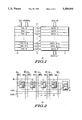
- FIG. 1 depicts a block diagram of a CAM memory system constructed in accordance with the present invention
- FIG. 2 depicts a block diagram of any one TAG memory element depicted in FIG. 1;
- FIG. 3 depicts a timing diagram of the CAM memory system depicted in FIGS. 1 and 2;
- FIG. 4 depicts a partial schematic diagram of the latch circuit depicted in FIG. 2;
- FIG. 5 depicts a logic diagram of a skewing circuit operable to generate the signals CLOCK1 and CLOCK2 depicted in FIG. 3.
- FIG. 1 depicts a block diagram of a CAM memory system 10 constructed in accordance with the present invention.
- CAM memory system 10 has N+1 sets 12 of memory elements, where N is an integer.
- Each set 12 has one TAG memory element and one DATA memory element.
- the N+1 TAG memory elements form a block 14 of TAG memory elements, where the TAG memory elements are labeled TAG 0 through TAG N.
- the N+1 DATA memory elements form a block 16 of DATA memory elements, where the DATA memory elements are labeled DATA 0 through DATA N. All TAG memory elements receive the input signals TAG and CONTROL.
- Each TAG memory element generates one of a plurality wordline signals 18 and forwards the one wordline signal to the DATA memory element within the same set 12.
- Each DATA memory element also receives the input DATA-IN and generates the output DATA-OUT.
- CAM memory system 10 generates a DATA-OUT signal that is valid during both the first and second phase of a control clock cycle (one component of the signal CONTROL). This makes CAM memory system 10 suitable for data processing applications where the actual cycle time approaches the minimum cycle time allowed by the manufacturing processes.
- CAM memory system 10 has three modes of operation: write, compare and read.
- write a tag and a data word are written into a TAG memory element and a DATA memory element, respectively, of one set of memory elements 12.
- the tag and dam word are input to TAG memory element and DATA memory element through the signals TAG and DATA-IN, respectively.
- the particular set of memory elements 12 so written to may be selected by any one of a number of known algorithms not related to the present invention, including least recently used set (LRU), random set, invalid set, etc.
- compare a tag is supplied to each of the TAG memory elements in block 14 through the input signal TAG. Each TAG memory element compares the data previously stored in it to the supplied tag.
- the matching TAG memory element will assert its matchline and, therefore, its wordline signal.
- an asserted matchline signal causes the DATA memory element associated with the matching TAG memory element to output a data word previously stored in the associated DATA memory element.
- the contents of a particular set of memory elements may be read by asserting the matchline associated with the particular set.
- FIG. 2 depicts a block diagram of any TAG memory element depicted in FIG. 1.
- FIG. 2 depicts the ith TAG memory element of block 14, where i is an integer index ranging from O to N.
- each TAG memory element stores four independent data bits in four CAM cells 20.
- CAM cells 20 are known in the art.
- the four TAG data bits are written to or read from the ith TAG memory element through the four pairs of bitline signals (labeled BL 0 /BL 0 through BL 3 /BL 3 where the bar notation indicates the logical complement of a signal).
- One pair of bitline signals is connected to a selected differing one of CAM cells 20 in each TAG memory element within block 14.
- Each input reference TAG bits are compared to the contents of the ith TAG memory element through the four pairs of reference signals (labeled Ref 0 /Ref 0 through Ref 3 /Ref 3 where the bar notation indicates the logical complement of a signal).
- One pair of the reference signals is connected to a selected differing one of CAM cells 20 in each TAG memory element within block 14.
- Each CAM cell 20 within the ith TAG memory element is connected to an ith latch circuit 22 of a set of N+1. latch circuits through an ith matchline node 24 of a set of N+1 matchline nodes.
- the ith matchline node 24 is logically AND'ed with a periodic clock signal or the complement of a periodic clock signal. The output of each logic combination then becomes the ith wordline.
- the ith latch circuit 22 is also connected to a first and a second periodic clock signal 26 and 27 (labeled CLOCK1 and CLOCK2, respectively).
- Periodic clocking signals 26 and 27 are characterized by two alternating phases. Each phase of clock signals 26 and 27 correspond to one of two possible logic states.
- Latch circuit 22 generates the ith wordline signal (labeled WL i ) 18 for the ith DATA memory element.
- the ith wordline signal is also connected to each CAM cell 20 within the ith TAG memory element.
- the ith wordline is asserted by a circuit (not shown) causing the ith TAG memory element to store the four-bit tag present on the four pairs of signals BL 0 /BL 0 through BL 3 /BL 3 .
- a data word associated with the four-bit tag is written into the ith DATA memory element 16.
- the ith DATA memory element is selected by the ith wordline signal as is known in the art.
- a compare operation is more fully described in terms of a first and second phase of the signal CLOCK1.
- each latch circuit 22 precharges, or couples a first voltage supply terminal to the latch circuit's associated matchline node 24.
- each of the N+1 TAG memory elements compares the four data bits provided by the signal TAG with the four bits stored in each set of four CAM cells 20. If any of the four stored data bits within each set does not match the corresponding input tag bit, then the CAM cell 20 finding the mismatch will discharge the associated matchline node 24.
- each latch circuit 22 will latch the associated one of the N+1 logic states generated by the instant compare step.
- the ith latch circuit 22 outputs the ith logic value on the ith wordline 18 until the next clock signal transition.
- each TAG memory element performs the same input-tag/stored-tag comparison during the second phase of clock signal 26. Therefore, each TAG memory element will either discharge or not discharge an associated match line node 24 depending upon the comparison. Similarly, each TAG memory element has its own latch circuit 22. Each latch circuit 22 precharges the matchline associated with the particular TAG memory element during the first clock phase and latches the logic value present at the transition between second clock phase and the subsequent first phase.
- the contents of the ith CAM memory element and the ith DATA memory element may be output as a conventional RAM or ROM by asserting the ith wordline.
- FIG. 3 depicts a timing diagram 28 of the CAM memory system depicted in FIGS. 1 and 2.
- Timing diagram 28 depicts the three signals TAG, MATCHLINE and WORDLINE with respect to the first and second periodic clock signals 26 and 27 (CLOCK1 and CLOCK2, respectively).
- the signals CLOCK1 and CLOCK2 are characterized by two cyclical phases (labeled ⁇ 1 and ⁇ 2 ).
- the duty cycle of the signal CLOCK2 is intentionally skewed with respect to CLOCK1 so that ⁇ 1 is longer than ⁇ 2 .
- Each high-to-low transition of the signal CLOCK2 occurs later in time than the same transition of the signal CLOCK1.
- the low-to-high transitions of the two clock signals are generally contemporaneous. A circuit that accomplishes this skew is described below in connection with FIG. 5.
- the amount of skew added to the high-to-low transition of the signal CLOCK2 ensures that the signal CLOCK2 transitions low immediately after CAM memory system 10 evaluates each of the N+1 matchline nodes 18. This condition is indicated in FIG. 3 by the high-to-low transition of the signal MATCHLINE.
- the amount of skew added to the low-to-high transition of the signal CLOCK2 ensures that the signal transitions high immediately before CAM memory system 10 precharges each of the N+1 matchline nodes 18. This condition may be fulfilled by causing the low-to-high transition of both clock signals to occur simultaneously.
- the signal TAG indicates that the address tenure of the four-bit tag occurs during the second phase of the signal CLOCK1.
- the signal MATCHLINE represents the voltage present on matchline node 24.
- latch circuit 22 precharges each matchline node 24 to a high logic state during the first phase of the signal CLOCK1.
- each TAG memory element may or may not discharge its corresponding matchline node 24 depending upon the match comparison. In some applications, the discharge of each matchline node 24 may occur relatively late in the second phase of the signal CLOCK1.
- the signal WORDLINE depicts the output of latch circuit 22. Latch circuit 22 latches the logic value present on matchline node 24 after the signal CLOCK2 transitions from a low logic state (second phase) to a high logic state (first phase of the subsequent clock cycle).
- This transition may occur shortly after each input-tag/stored-tag comparison completes.
- This timing scheme allows each of the N+1 matchline nodes to drive the corresponding DATA memory elements for a period of time as long as an entire cycle of the signal CLOCK2 (equal to the cycle time of CLOCK1).
- FIG. 4 depicts a partial schematic diagram of the latch circuit 22 depicted in FIG. 2.
- the output signal WORDLINE (labeled WL i ) is generated by an output of an inverter 30.
- An input of inverter 30 is connected to a first terminal of a switch or a pass gate 34 and to a first terminal of a switch or a pass gate 32.
- the output of inverter 30 is also connected to an input of an inverter 36.
- An output of inverter 36 is connected to a second terminal of pass gate 34.
- a gate of a P-channel device of pass gate 32 and a gate of an N-channel device of pass gate 34 are connected to the signal CLOCK2.
- a gate of an N-channel device of pass gate 32 and a gate of a P-channel device of pass gate 34 are connected to an output of an inverter 38 and to an output of an inverter 40, respectively.
- An input of inverter 38 and an input of inverter 40 are connected to the signal CLOCK2.
- a second terminal of pass gate 32 is connected to matchline node 24.
- Matchline node 24 receives the input signal MATCHLINE (labeled ML).
- Matchline node 24 is also connected to a drain of a P-channel transistor 42.
- a source of transistor 42 is connected to a voltage supply terminal corresponding to a high logic state.
- a gate of transistor 42 is connected to the output of an inverter 44.
- An input of inverter 44 receives the input signal CLOCK1.
- Latch circuit 22 has two phases of operation corresponding to the two logic states or phases of the signals CLOCK1 and CLOCK2.
- the signal CLOCK2 corresponds to a high logic state.
- pass gate 34 is in a conducting state and pass gate 32 is in a non-conducting state.
- Inverters 30 and 36 thereby form a latch retaining the logic value present at node 24 immediately before the low-to-high transition of the signal CLOCK2.
- Transistor 42 simultaneously precharges matchline node 24 to a high logic state during a portion of the first phase of the signal CLOCK2 (the first phase of the signal CLOCK 1).
- the changing voltage level at matchline node 24 does not effect the output of inverter 30.
- the signal CLOCK2 corresponds to a low logic state.
- pass gate 34 is in a non-conducting state and pass gate 32 is in a conducting state. Therefore, the voltage at node 24 directly passes to the output of inverter 30.
- the changing voltage level at matchline node 24 is directly passed to the output of inverter 30.
- FIG. 5 depicts a logic diagram of a skewing circuit 46 operable to generate the signals CLOCK1 and CLOCK2 depicted in HG. 3.
- the signals CLOCK1 and CLOCK2 are generated from a common periodic clock signal (labeled SYSTEM CLOCK).
- An output of an inverter 48 generates the signal CLOCK1.
- An input of inverter 48 is connected to an output of an inverter 50.
- An input of an inverter 50 is connected to the signal SYSTEM CLOCK.
- An output of an inverter 52 generates the signal CLOCK2.
- An input of inverter 52 is connected to an output of a NOR gate 54.
- a first input of NOR gate 54 is connected to the signal SYSTEM CLOCK.
- a second input of NOR gate 54 is connected to an output of an inverter 56.
- An input of inverter 56 is connected to an output of an inverter 58.
- An input of inverter 58 is connected to an output of an inverter 60.
- An input of inverter 60 is connected to an output of an inverter 62.
- An input of inverter 62 is also connected to the signal SYSTEM CLOCK.
- the propagation delay through NOR gate 54 and inverter 52 is generally equal to the propagation delay through inverters 48 and 50. Therefore, the low-to-high transition occurs simultaneously for both signals CLOCK1 and CLOCK2.
- inverters 56, 58, 60 and 62 cause a propagation delay for the signal CLOCK2 that is not duplicated for the signal CLOCK1.
- the propagation delay caused by these four inverters causes the high-to-low transition of the signal CLOCK2 to occur after the high-to-low transition of the signal CLOCK1.
- the skew added to the first phase of the signal CLOCK2 causes the high-to-low transition of the signal CLOCK2 to occur after each of the N+1 matchline nodes to evaluate to either a high or a low logic state.
- a CAM memory system may be used to store frequently used memory and source addresses of the memory, a cache, for use by a data processing system.
- a cache may access data stored in a main memory system that is also accessed by other systems.
- One example of such a system is a multiprocessor data processing system.
- several data processors usually individual microprocessors, each has a cache memory system incorporating a CAM memory system.
- all multiprocessors in the data processing system share a single main memory system.
- Various protocols known in the art exist to maintain data coherency when data may be modified while in a cache.
- "snooping" is the process by which each microprocessor (in the present example) monitors a data bus common to all microprocessors to determine if the data within one or more of the microprocessors is no longer valid.
- the operation of another microprocessor may modify the data value thereby invalidating older, unmodifed copies of the data.
- each microprocessor in the multiprocessor data processing system broadcasts its cache data write operations on the data bus to indicate such an invalidating operation to other microprocessors. For example, if a particular microprocessor modifies a copy of a data word resident in its cache by incrementing the value of the data word, then the microprocessor will broadcast the address of the modified data on the data bus.
- Every other microprocessor may then invalidate every old unincremented copy of the data. This prevents the other microprocessors from using an incorrect copy of the data.
- Each copy of data stored in a cache typically has a valid bit associated with it to facilitate such an invalidation operation.
- the disclosed invention facilitates a single cycle status update in a snooping data processing system.
- a data processing system containing CAM memory system 10 must determine if it has a copy of the affected data and if so, invalidate it, after the data processing system detects a data invalidating operation.
- a data processing system inputs all or a selected portion of the address of the snooped operation to each TAG memory element 14. If the data identified by the snooped tag is present in CAM memory system 10, then one matchline node 24 will not discharge. This matchline node will drive its corresponding DATA memory element 16.
- the data processing system may then write a logic value corresponding to an invalid entry into the bit allocated for the validity status of the associated DATA memory element.
- This bit may be located in either the TAG memory element or the DATA memory element.
- the ith TAG memory element or the ith DATA memory element may be written into by applying input data on the bitline signals while the ith wordline is asserted.
- Other types of write operations may occur to CAM memory system 10 in the same manner as necessary to the operation of the data processing system. These single-cycle write operations may be associated with other memory coherency protocols or simply with data stores to selected TAG or DATA memory elements.
Abstract
Description
Claims (8)
Priority Applications (3)
| Application Number | Priority Date | Filing Date | Title |
|---|---|---|---|
| US08/055,897 US5359564A (en) | 1993-05-04 | 1993-05-04 | Content addressable memory system and method of operation |
| JP6086506A JPH06349284A (en) | 1993-05-04 | 1994-04-25 | Content address memory system and its operating |
| EP94303058A EP0623933A1 (en) | 1993-05-04 | 1994-04-27 | Content addressable memory system and method of operation |
Applications Claiming Priority (1)
| Application Number | Priority Date | Filing Date | Title |
|---|---|---|---|
| US08/055,897 US5359564A (en) | 1993-05-04 | 1993-05-04 | Content addressable memory system and method of operation |
Publications (1)
| Publication Number | Publication Date |
|---|---|
| US5359564A true US5359564A (en) | 1994-10-25 |
Family
ID=22000880
Family Applications (1)
| Application Number | Title | Priority Date | Filing Date |
|---|---|---|---|
| US08/055,897 Expired - Lifetime US5359564A (en) | 1993-05-04 | 1993-05-04 | Content addressable memory system and method of operation |
Country Status (3)
| Country | Link |
|---|---|
| US (1) | US5359564A (en) |
| EP (1) | EP0623933A1 (en) |
| JP (1) | JPH06349284A (en) |
Cited By (12)
| Publication number | Priority date | Publication date | Assignee | Title |
|---|---|---|---|---|
| US5668972A (en) * | 1994-10-05 | 1997-09-16 | International Business Machines Corporation | Method and system for efficient miss sequence cache line allocation utilizing an allocation control cell state to enable a selected match line |
| US5708850A (en) * | 1994-07-27 | 1998-01-13 | Sony Corporation | Parallel processing system for time division multiplex data transfer including read/write dual port memory accessible to bus and digital signal processor during opposite phases of clock |
| US5802594A (en) * | 1995-09-06 | 1998-09-01 | Intel Corporation | Single phase pseudo-static instruction translation look-aside buffer |
| US6166939A (en) * | 1999-07-12 | 2000-12-26 | Net Logic Microsystems | Method and apparatus for selective match line pre-charging in a content addressable memory |
| US6215685B1 (en) * | 1997-11-26 | 2001-04-10 | Texas Instruments Incorporated | Sequentially comparing content addressable memory |
| US6266263B1 (en) * | 2000-10-02 | 2001-07-24 | Integrated Device Technology, Inc. | CAM array with minimum cell size |
| US6804133B1 (en) | 2002-08-30 | 2004-10-12 | Netlogic Microsystems, Inc. | Selective match line control circuit for content addressable memory array |
| US7461200B1 (en) | 2004-09-23 | 2008-12-02 | Netlogic Microsystems, Inc. | Method and apparatus for overlaying flat and tree based data sets onto content addressable memory (CAM) device |
| US7620838B2 (en) | 2004-10-19 | 2009-11-17 | Hitachi, Ltd. | Semiconductor integrated circuit and image processing system using the same |
| US8073005B1 (en) | 2001-12-27 | 2011-12-06 | Cypress Semiconductor Corporation | Method and apparatus for configuring signal lines according to idle codes |
| US8437203B2 (en) | 2010-07-02 | 2013-05-07 | SK Hynix Inc. | Nonvolatile memory apparatus and method for processing configuration information thereof |
| US8488407B2 (en) | 2010-07-02 | 2013-07-16 | SK Hynix Inc. | Nonvolatile memory apparatus and method for processing configuration information thereof |
Families Citing this family (1)
| Publication number | Priority date | Publication date | Assignee | Title |
|---|---|---|---|---|
| US6041389A (en) * | 1995-11-16 | 2000-03-21 | E Cirrus Logic, Inc. | Memory architecture using content addressable memory, and systems and methods using the same |
Citations (2)
| Publication number | Priority date | Publication date | Assignee | Title |
|---|---|---|---|---|
| US5130947A (en) * | 1990-10-22 | 1992-07-14 | Motorola, Inc. | Memory system for reliably writing addresses with reduced power consumption |
| US5249282A (en) * | 1990-11-21 | 1993-09-28 | Benchmarq Microelectronics, Inc. | Integrated cache memory system with primary and secondary cache memories |
Family Cites Families (3)
| Publication number | Priority date | Publication date | Assignee | Title |
|---|---|---|---|---|
| JPS63188893A (en) * | 1987-01-30 | 1988-08-04 | Mitsubishi Electric Corp | Storage device |
| JPS63281299A (en) * | 1987-05-13 | 1988-11-17 | Hitachi Ltd | Associative memory device |
| JP2635065B2 (en) * | 1987-12-18 | 1997-07-30 | 株式会社日立製作所 | Semiconductor memory circuit |
-
1993
- 1993-05-04 US US08/055,897 patent/US5359564A/en not_active Expired - Lifetime
-
1994
- 1994-04-25 JP JP6086506A patent/JPH06349284A/en active Pending
- 1994-04-27 EP EP94303058A patent/EP0623933A1/en not_active Withdrawn
Patent Citations (2)
| Publication number | Priority date | Publication date | Assignee | Title |
|---|---|---|---|---|
| US5130947A (en) * | 1990-10-22 | 1992-07-14 | Motorola, Inc. | Memory system for reliably writing addresses with reduced power consumption |
| US5249282A (en) * | 1990-11-21 | 1993-09-28 | Benchmarq Microelectronics, Inc. | Integrated cache memory system with primary and secondary cache memories |
Cited By (12)
| Publication number | Priority date | Publication date | Assignee | Title |
|---|---|---|---|---|
| US5708850A (en) * | 1994-07-27 | 1998-01-13 | Sony Corporation | Parallel processing system for time division multiplex data transfer including read/write dual port memory accessible to bus and digital signal processor during opposite phases of clock |
| US5668972A (en) * | 1994-10-05 | 1997-09-16 | International Business Machines Corporation | Method and system for efficient miss sequence cache line allocation utilizing an allocation control cell state to enable a selected match line |
| US5802594A (en) * | 1995-09-06 | 1998-09-01 | Intel Corporation | Single phase pseudo-static instruction translation look-aside buffer |
| US6215685B1 (en) * | 1997-11-26 | 2001-04-10 | Texas Instruments Incorporated | Sequentially comparing content addressable memory |
| US6166939A (en) * | 1999-07-12 | 2000-12-26 | Net Logic Microsystems | Method and apparatus for selective match line pre-charging in a content addressable memory |
| US6266263B1 (en) * | 2000-10-02 | 2001-07-24 | Integrated Device Technology, Inc. | CAM array with minimum cell size |
| US8073005B1 (en) | 2001-12-27 | 2011-12-06 | Cypress Semiconductor Corporation | Method and apparatus for configuring signal lines according to idle codes |
| US6804133B1 (en) | 2002-08-30 | 2004-10-12 | Netlogic Microsystems, Inc. | Selective match line control circuit for content addressable memory array |
| US7461200B1 (en) | 2004-09-23 | 2008-12-02 | Netlogic Microsystems, Inc. | Method and apparatus for overlaying flat and tree based data sets onto content addressable memory (CAM) device |
| US7620838B2 (en) | 2004-10-19 | 2009-11-17 | Hitachi, Ltd. | Semiconductor integrated circuit and image processing system using the same |
| US8437203B2 (en) | 2010-07-02 | 2013-05-07 | SK Hynix Inc. | Nonvolatile memory apparatus and method for processing configuration information thereof |
| US8488407B2 (en) | 2010-07-02 | 2013-07-16 | SK Hynix Inc. | Nonvolatile memory apparatus and method for processing configuration information thereof |
Also Published As
| Publication number | Publication date |
|---|---|
| EP0623933A1 (en) | 1994-11-09 |
| JPH06349284A (en) | 1994-12-22 |
Similar Documents
| Publication | Publication Date | Title |
|---|---|---|
| US5617348A (en) | Low power data translation circuit and method of operation | |
| US5598115A (en) | Comparator cell for use in a content addressable memory | |
| US5359564A (en) | Content addressable memory system and method of operation | |
| US5699288A (en) | Compare circuit for content-addressable memories | |
| US6191969B1 (en) | Selective match line discharging in a partitioned content addressable memory array | |
| US6173379B1 (en) | Memory device for a microprocessor register file having a power management scheme and method for copying information between memory sub-cells in a single clock cycle | |
| US6564289B2 (en) | Method and apparatus for performing a read next highest priority match instruction in a content addressable memory device | |
| US5717885A (en) | TLB organization with variable page size mapping and victim-caching | |
| EP0905709B1 (en) | Single ended match sense amplifier | |
| US6415374B1 (en) | System and method for supporting sequential burst counts in double data rate (DDR) synchronous dynamic random access memories (SDRAM) | |
| US6188629B1 (en) | Low power, static content addressable memory | |
| US6054918A (en) | Self-timed differential comparator | |
| US5638315A (en) | Content addressable memory for a data processing system | |
| US5754463A (en) | Multi-ported content addressable memory with precharge "non match" | |
| US4894799A (en) | Content-addressable memory | |
| US5130692A (en) | Improved data comparator for comparing plural-bit data at higher speed | |
| US6012133A (en) | Mutually controlled match-line-to-word-line transfer circuit | |
| WO2006127117A2 (en) | Storage circuit and method therefor | |
| US6236585B1 (en) | Dynamic, data-precharged, variable-entry-length, content addressable memory circuit architecture with multiple transistor threshold voltage extensions | |
| US6539466B1 (en) | System and method for TLB buddy entry self-timing | |
| US5881076A (en) | Comparator utilizing redundancy | |
| US6493790B1 (en) | Translation-lookaside buffer with current tracking reference circuit | |
| US6138211A (en) | High-performance LRU memory capable of supporting multiple ports | |
| US6230237B1 (en) | Content addressable memory with an internally-timed write operation | |
| US5978245A (en) | Associative memory device having circuitry for storing a coincidence line output |
Legal Events
| Date | Code | Title | Description |
|---|---|---|---|
| AS | Assignment |
Owner name: MOTOROLA, INC., ILLINOIS Free format text: ASSIGNMENT OF ASSIGNORS INTEREST;ASSIGNOR:WANG, KARL;REEL/FRAME:006538/0513 Effective date: 19930430 |
|
| STPP | Information on status: patent application and granting procedure in general |
Free format text: APPLICATION UNDERGOING PREEXAM PROCESSING |
|
| FPAY | Fee payment |
Year of fee payment: 4 |
|
| FPAY | Fee payment |
Year of fee payment: 8 |
|
| AS | Assignment |
Owner name: FREESCALE SEMICONDUCTOR, INC., TEXAS Free format text: ASSIGNMENT OF ASSIGNORS INTEREST;ASSIGNOR:MOTOROLA, INC.;REEL/FRAME:015698/0657 Effective date: 20040404 Owner name: FREESCALE SEMICONDUCTOR, INC.,TEXAS Free format text: ASSIGNMENT OF ASSIGNORS INTEREST;ASSIGNOR:MOTOROLA, INC.;REEL/FRAME:015698/0657 Effective date: 20040404 |
|
| FPAY | Fee payment |
Year of fee payment: 12 |
|
| AS | Assignment |
Owner name: CITIBANK, N.A. AS COLLATERAL AGENT, NEW YORK Free format text: SECURITY AGREEMENT;ASSIGNORS:FREESCALE SEMICONDUCTOR, INC.;FREESCALE ACQUISITION CORPORATION;FREESCALE ACQUISITION HOLDINGS CORP.;AND OTHERS;REEL/FRAME:018855/0129 Effective date: 20061201 Owner name: CITIBANK, N.A. AS COLLATERAL AGENT,NEW YORK Free format text: SECURITY AGREEMENT;ASSIGNORS:FREESCALE SEMICONDUCTOR, INC.;FREESCALE ACQUISITION CORPORATION;FREESCALE ACQUISITION HOLDINGS CORP.;AND OTHERS;REEL/FRAME:018855/0129 Effective date: 20061201 |
|
| AS | Assignment |
Owner name: CITIBANK, N.A., AS COLLATERAL AGENT,NEW YORK Free format text: SECURITY AGREEMENT;ASSIGNOR:FREESCALE SEMICONDUCTOR, INC.;REEL/FRAME:024397/0001 Effective date: 20100413 Owner name: CITIBANK, N.A., AS COLLATERAL AGENT, NEW YORK Free format text: SECURITY AGREEMENT;ASSIGNOR:FREESCALE SEMICONDUCTOR, INC.;REEL/FRAME:024397/0001 Effective date: 20100413 |
|
| AS | Assignment |
Owner name: FREESCALE SEMICONDUCTOR, INC., TEXAS Free format text: PATENT RELEASE;ASSIGNOR:CITIBANK, N.A., AS COLLATERAL AGENT;REEL/FRAME:037354/0225 Effective date: 20151207 Owner name: FREESCALE SEMICONDUCTOR, INC., TEXAS Free format text: PATENT RELEASE;ASSIGNOR:CITIBANK, N.A., AS COLLATERAL AGENT;REEL/FRAME:037356/0143 Effective date: 20151207 Owner name: FREESCALE SEMICONDUCTOR, INC., TEXAS Free format text: PATENT RELEASE;ASSIGNOR:CITIBANK, N.A., AS COLLATERAL AGENT;REEL/FRAME:037356/0553 Effective date: 20151207 |