US5361228A - IC memory card system having a common data and address bus - Google Patents
IC memory card system having a common data and address bus Download PDFInfo
- Publication number
- US5361228A US5361228A US08/054,575 US5457593A US5361228A US 5361228 A US5361228 A US 5361228A US 5457593 A US5457593 A US 5457593A US 5361228 A US5361228 A US 5361228A
- Authority
- US
- United States
- Prior art keywords
- data
- address
- host
- signal
- memory card
- Prior art date
- Legal status (The legal status is an assumption and is not a legal conclusion. Google has not performed a legal analysis and makes no representation as to the accuracy of the status listed.)
- Expired - Lifetime
Links
Images


Classifications
-
- G—PHYSICS
- G11—INFORMATION STORAGE
- G11C—STATIC STORES
- G11C16/00—Erasable programmable read-only memories
- G11C16/02—Erasable programmable read-only memories electrically programmable
- G11C16/06—Auxiliary circuits, e.g. for writing into memory
- G11C16/10—Programming or data input circuits
- G11C16/102—External programming circuits, e.g. EPROM programmers; In-circuit programming or reprogramming; EPROM emulators
-
- G—PHYSICS
- G11—INFORMATION STORAGE
- G11C—STATIC STORES
- G11C5/00—Details of stores covered by group G11C11/00
- G11C5/06—Arrangements for interconnecting storage elements electrically, e.g. by wiring
- G11C5/066—Means for reducing external access-lines for a semiconductor memory clip, e.g. by multiplexing at least address and data signals
Definitions
- the present invention relates to an IC (Integrated Circuit) memory card for storing image data, character data or similar data and, more particularly, to an IC memory card system using an IC memory card incorporating an SRAM (Static Random Access Memory), EEPROM (Electrically Erasable Programmable Read Only Memory) or similar semiconductor memory.
- SRAM Static Random Access Memory
- EEPROM Electrically Erasable Programmable Read Only Memory
- the present invention is also concerned with such an IC memory card and a data inputting and outputting system applicable to the IC memory card system.
- a digital electronic still camera should be provided with an interface capable of accommodating both of a memory card with an SRAM and a memory card with an EEPROM, as needed.
- An interface having the above-stated capability may be implemented as an interface connector having twenty pins, as proposed by Japan Electronic Industry Development Association (JEIDA) in "IC MEMORY GUIDELINE", 3rd Edition.
- JEIDA Japan Electronic Industry Development Association
- IC MEMORY GUIDELINE 3rd Edition.
- this GUIDELINE when the input and output of data from the IC memory card is implemented by an 8-bit parallel transfer bus, the interface connector is provided with eight data terminals. Then, not only data to be written to or read out of a memory chip but also an address designating the address location of the data in the memory card are applied to the eight data terminals. The address and the data are distinguished from each other by the logical states of two state terminals.
- each byte is indicated by a particular combination of the logical states of the state terminals. For example, assuming an IC memory card using an SRAM whose capacity exceeds sixty-four kilobytes, the address is made up of three bytes. Then, the state terminals are indicative of the lower one of the three bytes to be read when both are in a low level, the middle one of the three bytes when one state terminal is in a low level and the other state terminal is in a high level, and the higher one of the three bytes when the former is in a high level and the latter is in a low level.
- both of the two state terminals are in a high level, they are indicative of reading or writing of data.
- the reading and the writing of data are distinguished from each other by the logical state of a read terminal and that of a write terminal provided independently of the state terminals. Specifically, data are read out when the read terminal goes high or data are written in when the write terminal goes high.
- the memory card writes or reads data in or out of the memory chip in response to control signals sent from an electronic still camera or similar host to such control terminals.
- a status representative of the kind, capacity and so forth of the memory chip and a flag representing the instantaneous control condition of the card are read out of the card.
- the conventional IC memory card with the above-described type of interface connector is provided with a control circuit for controlling the writing and reading of data out of the memory chip.
- the control circuit reads the status of the card to inform the host of the adaptability of the card and, on receiving an address made up of a plurality of bytes from the host, designates a corresponding address location of the memory chip. Subsequently, as the host sends a timing clock signal to a clock terminal also included in the connector, the control circuit sequentially increments the address to read data out of the memory chip or to write data therein.
- the conventional IC memory card system has the following problem. Since the interface connector has only twenty pins as input/output terminals, an extra function cannot be added to the memory card unless one or more of the pins is exclusively allocated thereto. On the other hand, only four different states, including the writing of data, are available with the two state terminals of such a connector. Hence, when the address is made up of four or more bytes, i.e., when the storage capacity of the memory chip exceeds sixty-four kilobytes, an extra terminal for receiving a state signal is required. It follows that the conventional data inputting and outputting system is not practical when it is desired to add an extra function and increase the storage capacity.
- Japanese Patent Application No. 257380/1990 discloses an IC memory card capable of distinguishing all of the expected states with an address/data terminal distinguishing an address and data by a logical bilevel state (high or low), a read/write terminal distinguishing writing and reading by a bilevel state, and a bus clock terminal synchronous to an address or data on a byte basis, and capable of setting an address with no regard to the number of bytes.
- the problem with this type of memory card is that, when implemented by an EEPROM, it has to make a decision on the erasure of data and generate an erase signal within itself.
- the memory card therefore, needs complicated control circuitry and cannot operate at high speed, compared to a memory card using an SRAM.
- an object of the present invention to provide an IC memory card system which allows an IC memory card to accommodate an extra function without resorting to a greater number of terminals than the conventional one and to read even an address made up of four or more bytes.
- an IC memory card system comprises a host for processing data, and an IC memory card removably connected to the host and incorporating a data recording medium implemented by an electrically erasable programmable semiconductor memory.
- the host has a system controller for sending to the memory card an address/data signal for distinguishing an address and data by a logical bilevel state, a read/write signal for distinguishing reading of data and writing of data in the semiconductor memory by a logical bilevel state, an erase signal for erasing data stored in the semiconductor memory by a logical bilevel state as control signals, and bus clock pulses each being synchronous to a particular address and particular data.
- the memory card has a control circuit responsive to the address/data signal, read/write signal, erase signal and bus clock pulses for distinguishing an address and data, for distinguishing reading and writing, for determining whether or not to erase existing data, and then reading or writing data in the semiconductor memory or for erasing the existing data.
- an IC memory card comprises a storage implemented by a semiconductor memory for storing data, a control circuit for selectively writing or reading data in or out of the storage, and an inputting and outputting circuit for removably connecting the control circuit to a host.
- the inputting and outputting circuit comprises: a common data terminal to which the host selectively sends an address for accessing the storage and input or output data, or a number of blocks of the storage to erase, an address/data terminal to which the host sends a bilevel signal for distinguishing the address and data and the number of blocks to erase to be applied to the common data terminal, a read/write terminal to which the host sends a bilevel signal for distinguishing reading of data and writing of data, an erase terminal to which the host sends a bilevel signal indicative of erasure of data, and a bus clock input terminal to which the host sends bus clock pulses, each being synchronous to a particular address, particular data or the number of blocks to erase.
- a method of inputting and outputting data from an IC memory card incorporating a semiconductor memory which receives an address to access and data to record over a common bus and, before the data are written to the semiconductor memory, has data existing therein erased comprises the steps of: (1) sending (from a host to the IC memory card) an address/data signal (for distinguishing an address and data by a logical bilevel state), a read/write signal (for distinguishing reading of data and writing of data in the semiconductor memory by a logical bilevel state), an erase signal (for erasing data existing in the semiconductor memory by a logical bi-level state), control signals, and bus clock pulses (each being synchronous to a particular address and particular data), and (2) writing or reading data in or out of the semiconductor memory or erasing data of the semiconductor memory by distinguishing an address and data, distinguishing writing of data and reading of data and determining whether or not to erase data on the basis of the bilevel states of the address/data signal, read/write signal and
- an IC memory card system comprises a host for processing data, and an IC memory card incorporating a semiconductor memory therein and removably connected to the host for selectively writing or reading, on receiving an address made up of a plurality of blocks from the host, data in or out of the semiconductor memory by sequentially incrementing the address within the IC memory card.
- the IC memory card comprises a plurality of address counters, each for storing one of the plurality of blocks constituting the address received from the host, and for accessing the semiconductor memory by sequentially incrementing the block; a control circuit for controlling writing or reading of data on receiving control signals for writing or reading data or control signals for setting an address from the host; and a selector for selectively sending to the host the address from the plurality of address counters or the data read out of the semiconductor memory.
- the host sends a read/write signal for distinguishing writing of data and reading of data by a logical bilevel state, an address/data signal for distinguishing an address and data by a logical bilevel state, and a timing clock pulse for driving a data bus to the IC memory card.
- the control circuit of the IC memory card is responsive to the read/write signal and address/data signal for setting up a status signal read mode and activating the selector, and is responsive to the timing clock pulse for sending the instantaneous address from the plurality of address counters to the host via the selector.
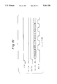
- FIG. 1 is a block diagram schematically showing an IC memory card system embodying the present invention
- FIG. 2 is a list showing specific terminals assigned to an interface connector included in the embodiment
- FIG. 3 is a table representative of a relation between the logical states of control signals and modes to be set up thereby which are particular to the embodiment;
- FIG. 4 is a timing chart demonstrating a specific data erasing operation of the embodiment
- FIG. 5 is a block diagram schematically showing an IC memory card representative of an alternative embodiment of the present invention.
- FIG. 6 is a schematic block diagram showing a specific construction of a control circuit built in the memory card of FIG. 5;
- FIG. 7 is a table representative of a relation between the logical states of control signals and modes to be set up thereby which are particular to the alternative embodiment;
- FIG. 8 is a timing chart indicative of part of a status signal read mode to be executed by the alternative embodiment
- FIGS. 9 and 10 are timing charts representative of an address set mode and a data write mode, respectively, which are particular to the alternative embodiment
- FIG. 11 is a timing chart indicative of the other part of the status signal read mode of the alternative embodiment.
- FIG. 12 is a timing chart showing a data read mode to be executed by the alternative embodiment.
- an IC memory card system embodying the present invention includes an electronic still camera or similar host processing unit 100.
- An IC memory card 200 is removably connected to the host processing unit 100 (or simply host 100 as referred to hereinafter), and has a main memory implemented by an EEPROM. Picture data or similar data are selectively written to or read out of the memory card 200 under the control of the host 100.
- the host 100 has a system controller 104 which controls the entire system for writing or reading data in or out of the memory card 200. In FIG. 1, only part of the host 100 relating to the illustrative embodiment is shown for the sake of simplicity.
- the memory card 200 is generally made up of an interface connector 300, a control circuit 400, and a storage 500 including an EEPROM as a semiconductor memory.
- the interface connector 300 is removably connected to the system controller 104 of the host 100.
- the control circuit 400 writes or reads data in or out of the storage 500 under the control of the system controller 104.
- the system controller 104 of the host 100 writes data generated by the host 100 in the memory card 200 or reads them out of the memory card 200, as needed.
- the system controller 104 generates control signals for writing or reading such data and sends them to the memory card 200 via the connector 300.
- the system controller 104 generates an erase signal ES and sends it to the memory card 200 for erasing data stored therein.
- the system controller 104 delivers an address to the memory card 200 while interchanging data and, in addition, delivers the number of blocks to erase to the card 200.
- control lines -A/D, R/-W, BCK, CE, ES, and RDY/BSY are control lines -A/D, R/-W, BCK, CE, ES, and RDY/BSY.
- the system controller 104 sends an address/data signal over the control line -A/D, a data read/write signal over the control line R/-W, a data or address timing signal over the control line BCK, a card enable signal over an control line CE, and the erase signal over the control line ES, while receiving a signal indicative of the state of the memory card 200 over the control line RDY/BSY.
- the system controller 104 is capable of selectively setting up an address set mode, a data write mode, a data read mode or an erase mode.
- the system controller 104 causes the control lines -A/D, R/-W and ES to go low ("0" in FIG. 3) and then delivers an address to the common bus D0-D7 in response to the timing clock signal appearing on the control line BCK.
- an address is represented by twenty-four bits and is divided into a higher, a medium and a lower address, each having eight bits.
- the system controller 104 causes the control line -A/D to go high ("1" in FIG. 3) while causing the control lines R/-W and ES to go low and then sends data to the bus D0-D7 in response to the timing clock signal on the control line BCK.
- the system controller 104 causes the control lines -A/D and ES to go high while causing the control line R/-W to go low and then delivers the desired number of blocks to erase in response to the timing clock signal on the control line BCK.
- the number of blocks to erase is represented by sixteen bits divided into a higher and a lower byte and sent over the data bus D0-D7.
- the connector 300 of the memory card 200 receives the control signals and data from the system controller 104 by using a 20-pin I/O bus interface shown in FIG. 2.
- the interface of FIG. 2 is identical with the interface proposed by the previously mentioned "IC MEMORY GUIDELINE", except for terminal Nos. 14-17 to which the discrimination signals particular to the embodiment are applied.
- the connector 300 includes: two ground terminals (Nos. 1 and 20); data terminals Nos. 2-9 connected to the bidirectional bus D0-D7 to which the eight bits of the address, data or number of blocks to erase are applied in parallel, a logical power source terminal No. 10 to which a 5 volt DC voltage (Vcc) for reading data is applied from the host 100; a program power source terminal No.
- the connector 300 also includes an address/data terminal No. 14 to which the address/data signal -A/D is applied; a read/write terminal No. 15 to which the read/write signal R/-W is applied; a clock terminal No. 16 to which the timing clock signal BCK is applied; and an erase terminal No. 17 to which the erase signal ES is applied.
- the connector 300 further includes reserve terminal Nos. 18 and 19 which are idle in the illustrative embodiment.
- the terminal Nos. 14 and 15 are used as state terminals A0 and A1 for distinguishing data and address while the terminal Nos. 16 and 17 are used as a read terminal RD and a write terminal WR, respectively.
- the storage 500 of the memory card 200 is made up of a block erasure type EEPROM playing the role of a main memory, and a buffer 508 for temporarily storing data to be written to or read out of the EEPROM 502.
- the buffer 508 allows data to be written to or read out of the EEPROM 502 therethrough eight bits at a time.
- the EEPROM 502 has a plurality of blocks or cells #1 to #n, each being the minimum unit of data erasure and having a capacity of, for example, eight kilobytes.
- control circuit 400 sequentially designates the addresses of any of the blocks or cells #1 to #n, data are written to or read out of the designated blocks on a block basis with the address sequentially incremented eight bits at a time.
- a sequence for writing or reading data in or out of the EEPROM 502 is executed by a command from a write sequencer 410 or a read sequencer 412 included in the control circuit 400.
- An erase sequencer 408 is also included in the control circuit 400 for erasing, in the previously mentioned data write mode, old data stored in the EEPROM 502 before new data is written.
- An address latch 402 made up of a plurality of registers, an address decoder 404 and an operation mode decoder 406 are further included in the control circuit 400.
- the registers of the address latch 402 latch the address byte by byte. Also, when data stored in any of the blocks or cells #1 to #n of the EEPROM 502 are to be erased, the registers of the address latch 402 latch the number of blocks to erase.
- the address latch 402 has a first to a third address register each for latching eight bits of a 24-bit address, and a fourth and a fifth register for latching eight of sixteen bits representative of the number of blocks to erase each.
- the address and the number of blocks to erase are transferred from the address latch 402 to the block decoder 404.
- the block decoder 404 On receiving the address from the address latch 402, the block decoder 404 decodes it and then produces one of enable signals BE#1 to BE#n meant for one of the the blocks #1 to #n of the EEPROM 502 which is designated by the address.
- the block decoder 404 includes a counter for sequentially incrementing the address eight bits at a time from the first address latched by the address latch 402, thereby sequentially accessing the addresses block by block.
- the block decoder 404 sequentially counts the first address and successive addresses until the number of blocks latched in the address latch 402 has been reached, thereby accessing the blocks to erase. As the number of blocks to erase is reached, the block decoder 404 sends a stop signal St to the erase sequencer 408.
- the decoder 406 conditions the various sections of the memory card 200 for one of the previously mentioned address set mode, data write mode, data read mode, and erase mode (see FIG. 3). Namely, in the address set mode, the operation mode decoder 406 delivers a select signal Ss to the address latch 402 for causing it to activate the first to third registers. As a result, the first to third registers latch the address sent from the host 100. In the data write mode, the operation mode decoder 406 feeds a write mode signal Sw to the write sequencer 410 for driving it. In the data read mode, the operation mode decoder 406 feeds a read mode signal Sr to the read sequencer 412.
- the operation mode decoder 406 delivers a select signal Ss to the address latch 402 for activating the fourth and fifth registers, thereby causing them to latch the number of blocks to erase.
- the decoder 406 feeds an erase mode signal Se to the erase sequencer 408 for activating it.
- each the address/data signals -A/D, the read/write signal R/-W and the erase signal ES are in a low level, setting up the address set mode. Then, on receiving the timing signal BCK from the host 100, the operation mode decoder 406 delivers the select signal Ss to the address latch 402 for activating the first to third registers one after another. In the erase mode, wherein the address/data signal -A/D and erase signal ES are in a high level and the read/write signal R/-W is in a low level, the decoder 406 delivers the select signal Ss to the address latch 402 in response to the timing signal BCK, thereby sequentially activating the fourth and fifth registers.
- the decoder 406 feeds the erase mode signal Se to the erase sequencer 408, as mentioned previously.
- the decoder 406 sends the write mode signal Sw to the write sequencer 410 in response to the timing clock signal BCK.
- the decoder 406 delivers the read mode signal Sr to the read sequencer 412 in response to the timing clock signal BCK. In this case, the erase signal ES is held in a low level.
- the erase sequencer 408 On receiving the erase mode signal Se from the operation mode decoder 406, the erase sequencer 408 erases any of the blocks #1 to #n of the storage or memory chip 500. Specifically, in response to the erase mode signal Se, the erase sequencer 408 feeds an erase command to the EEPROM 502 to cause it to erase data stored in any of the blocks #1 to #n designated by the block decoder 404. To erase a plurality of blocks, the erase sequencer 408 delivers a timing signal Si to the block decoder 404 to cause it to sequentially select particular ones of the enable signals BE#1 to BE#n meant for the blocks of interest. As the block decoder 404 counts up the number of blocks to erase, it sends a stop signal St to the erase sequencer 408. In response, the erase sequencer 408 stops feeding the erase command to the EEPROM 502. During the course of the erasure, the erase sequencer 408 continuously feeds a busy signal BSY to the RDY/BSY terminal 12.
- the sequencer 410 controls the sequence for causing the memory chip 500 to write data therein. Specifically, on receiving the write mode signal Sw, the write sequencer 410 activates the buffer 508 to lodge data sent from the host 100 in the buffer 508. Subsequently, the write sequencer 410 delivers a write command to the EEPROM 502 for causing it to write the data stored in the buffer 508 in a block accessed by the block decoder 404. Then, the write sequencer 410 compares the data written to the block of interest and the data stored in the buffer 508.
- the write sequencer 410 continuously feeds a busy signal BSY to the RDY/BSY terminal 12 to temporarily reject data from the host 100.
- the write sequencer 412 sends a signal Si to the block decoder 404 for incrementing the address, increments the enable signal by eight bits, and then cancels the busy signal BSY.
- the host 100 again sends data and bus signal clock BCK to the control section 400, the write mode is set up again.
- the data from the host 100 are written to the EEPROM 502 eight bits at a time, and then the address is incremented. Such a procedure is repeated thereafter until all the data have been written to the EEPROM 502.
- the read sequencer 412 controls, on receiving the read mode signal Sr from the operation mode decoder 406, the sequence for causing the memory chip 500 to read data therefrom. Specifically, in response to the read mode signal St, the read sequencer 412 sends a read command to the EEPROM 502 and activates the buffer 508 to read data out of the address designated by the block decoder 404. The read sequencer 412 also delivers the timing signal Si to the block decoder 404 to cause it to sequentially increment the address eight bits at a time.
- the operator of the electronic still camera or similar host 100 couples the connector 300 of the memory card 200 to the system controller 104 of the host 100 and then manipulates the host 100 in a predetermined manner.
- the system erases data stored in designated one or ones of the blocks or cells of the EEPROM 502, as follows.
- the system controller 104 of the host 100 sequentially sends an address represented by, for example, twenty-four bits to the memory card 200 byte by byte.
- the system controller 104 sends an address/data signal -A/D to the terminal 14 of the connector 300 in a low level, sends a read/write signal R/-W to the terminal 15 in a low level, and sends an erase signal ES to the terminal 17 in a low level.
- These control signals are applied to the operation mode decoder 406 via the connector 300.
- the operation mode decoder 406 is conditioned for the address set mode and awaits a bus clock pulse BCK from the system controller 104.
- the system controller 104 sends a higher 8-bit address signal A0-A7 to the latch 402 via the bidirectional bus D0-D7 and the first bus clock pulse BCK to the operation mode decoder 406, the decoder 406 feeds a select signal Ss to the address latch 402 for activating the first register thereof. Consequently, the higher 8-bit address A0-A7 is latched in the first register of the address latch 402.
- the system controller 104 While the above-stated control signals are each held in the address set mode state, the system controller 104 sends the middle 8-bit address A8-A15 together with the second bus clock pulse BCK. Then, the operation mode decoder 406 again delivers a select signal Ss to the data latch 402 for activating the second register thereof. Consequently, the middle 8-bit address signal A8-A15 is latched in the second register. Thereafter, the system controller 104 sends the lower 8-bit address signal A16-A23 together with the third bus clock pulse while maintaining the control signals in the address set mode state. The lower 8-bit address A16-A23 is latched in the third register of the address latch 402 in the same manner as the previous 8-bit addresses.
- the higher, middle and lower addresses so latched in the three registers of the address latch 402 are transferred to the block decoder 404.
- the block decoder 404 decodes the addresses and then feeds an enable signal BE#1 (BE#2 to BE#n) to the EEPROM 502.
- the system controller 104 causes the address/data signal -A/D and erase signal ES to go high while maintaining the read/write signal R/-W in a low level.
- the operation mode decoder 406 is conditioned for the erase mode and awaits a bus clock pulse BCK. Then, the system controller 104 sends the higher byte N H of the number of blocks to decode to the address latch 402 over the bidirection bus D0-D7 while sending a bus clock pulse BCK to the operation mode decoder 406.
- the operation mode decoder 406 feeds a select signal Ss to the address latch 402 for activating the fourth register thereof, thereby latching the higher byte N H of the number of blocks in the latch 402. Subsequently, the system controller 104 sends a lower byte N L of the number of blocks to erase to the address latch 402 while sending a bus clock pulse BCK to the operation mode decoder 406. In response, the operation mode decoder 406 again sends a select signal Ss to the address latch 402 for activating the fifth register, thereby latching the lower byte N L in the fifth register. The number of blocks so latched in the address latch 402 is also transferred to the block decoder 404.
- the system controller 104 causes the address/data signal -A/D and erase signal ES to go low and then awaits the erasure of data to occur in the memory card 200.
- the operation mode decoder 406 delivers an erase mode signal Se to the erase sequencer 408.
- the erase sequencer 408 sends a busy signal BSY to the host 100 via the connector 300 so as to inform the system controller 104 of the erasure under way. This causes the system controller 104 to stop accessing the memory card 200 for a moment.
- the erase sequencer 408 feeds the first erase command to the EEPROM 502 to erase the data stored in the block designated by the block decoder 404. Subsequently, the erase sequencer 408 delivers a timing signal Si to the block decoder 404 to cause it to feed an enable signal meant for the next block to the EEPROM 502, and then delivers an erase command to the EEPROM 502 to erase the data stored in the next block. At this instant, the block decoder 404 compares the number of timing signals Si fed thereto with the number of blocks to erase latched in the address latch 402.
- the erase sequencer 408 repeats the above procedure until the number of timing signals Si fed to the block decoder 404 and the number of blocks to erase compare equal, thereby sequentially erasing the data of the designated blocks of the EEPROM 502. As the erasure of data is completed, the block decoder 404 determines that the number of timing signals Si is coincident with the number of blocks to erase. Then, the block decoder 404 feeds a stop signal St to the erase sequencer 408. As a result, the erase sequencer 408 stops sending the erase command and cancels the busy signal BSY having been sent to the system controller 104.
- the host 100 On the cancellation of the busy signal BSY, the host 100 starts sending data to the memory card 200 one byte at a time. Specifically, the system controller 104 causes the address/data signal -A/D to go high while maintaining the read/write signal R/-W and erase signal ES in a low level, thereby conditioning the memory card 200 for the data write mode. In response, the operation mode decoder 406 feeds a write mode signal Sw to the write sequencer 410 to activate it. Then, the write sequencer 410 turns on the buffer 508, writes the first eight bits of data sent from the host 100 in the buffer 508, and then delivers a write command to the EEPROM 502.
- the write sequencer 410 verifies the data newly written to the EEPROM 502 and, on determining that the data have been correctly written, sends a timing signal Si to the block decoder 404 to increment the address. At this instant, the write sequencer 410 cancels a busy signal BSY having been sent to the system controller 104. The host 100, therefore, sends the next eight bits of data to the memory card 200. The write sequencer 410 is again brought into the write mode for writing the eight bits of data in an EEPROM cell 502 designated by the next address. Such a sequence of steps is repeated until a predetermined amount of data has been written to the EEPROM 502.
- the host 100 sends a 24-bit address signal to the block decoder 404 via the address latch 402, as in the data write mode. Then, the read sequencer 412 sequentially reads data out of addresses sequentially designated by the block decoder 404.
- the system controller 104 built in the host 100 changes the logical levels of the address/data signal -A/D, read/write signal R/-W and erase signal ES to condition the memory card 200 for one of the address set mode, data write mode, data read mode, and data erase mode, thereby causing the card 200 to execute the mode selected.
- the embodiment since the embodiment causes the host 100 to send an erase command and the number of blocks to erase to the memory card 200, the card 200 does not have to make decision on the erasure of data within itself, thereby reducing the load on the control circuit 400.
- the embodiment does not assign the decision to simple logic using only the erase terminal ES.
- the embodiment sets an address, sets the number of blocks to erase when the erase terminal ES and address/data terminal -A/D go high, and then determines, when the terminals ES and -A/D go low, that data have been erased.
- the data erasure as a sequence of such steps, it is possible to protect valuable data stored in the memory card 200 from erasure ascribable to the operator's careless or accidental operation of the host 100.
- the embodiment reduces the conventional two state terminals A0 and A1 and independent write terminal WR and read terminal RD to three terminals, i.e., the address/data terminal -A/D, read/write terminal R/-W, and clock terminal BCK, and uses the resulting idle terminal as the erase terminal ES. This allows an erase command to be sent to the memory card 200 from the outside without increasing the number of pins conventionally given to the interface connector.
- the memory card 200 sends a busy signal BSY to the host 100 in the event of erasure.
- the system controller 104 since the system controller 104 knows the duration of erasure beforehand in terms of the number of blocks to erase, it may await a given period of time associated with the number of blocks to erase and again access the memory card 200.
- the embodiment determines the destination of the data on the basis of the erase address, i.e., without causing the system controller 104 to send the destination address to the memory card 200.
- the system controller 104 may condition the memory card 200 for the address set mode before sending data and then send an address to the card 200.
- the IC memory card is generally made up of a memory chip 600, a control circuit or input/output (I/O) port 602, a power supply control circuit 604, and an interface connector 606.
- the control circuit 602 controls the operation for writing or reading data in or out of the memory chip 600.
- the power supply control circuit 604 applies a particular voltage to each of the memory chip 600 and control circuit 602.
- the interface connector 600 (or simply connector 606 as referred to hereinafter), is removably connected to a host, e.g., an electronic still camera or a personal computer, not shown.
- the reference numeral 608 designates a back-up battery which will be mounted on the memory card when the memory chip 600 is implemented as an SRAM.
- the memory chip 600 is constituted by an EEPROM, SRAM or similar semiconductor memory.
- the memory chip 600 has an output enable terminal OE, a write enable terminal WE and other control terminals for receiving various control signals over a control line 610, a 32-bit input terminal implemented as address terminals A0-A31 which are connected to an address line 612, and data terminals D0-D7 connected to an 8-bit bidirectional data bus 614. Data are written to or read out of a particular address location of the memory chip 600 designated by an address fed to the address terminals A0-A31. One byte of data is written or read at a time via the data terminals D0-D7.
- the write-in and read-out of data are respectively allowed when the write enable terminal WE is in a high level and when the output enable terminal OE is in a high level.
- the power supply control circuit 604 applies to the memory chip 600 a drive voltage Vcc of 5 volts and, when the chip 600 is implemented by an EEPROM, a program voltage Vpp of 12 volts.
- the drive voltage Vcc is used to read data out of the memory chip 600 while the program voltage Vpp is used to erase and write data in the chip 600.
- SRAM is used as the memory chip 600, data will be written and read out only by the drive voltage Vcc.
- control circuit 602 As the host sends control signals and an address to the memory chip 600 via the connector 606, the control circuit 602 writes or reads data in or out of the chip 600.
- the voltage Vcc of 5 volts is also applied to the control circuit 602 from the power supply control circuit 604.
- the control circuit 602 is connected to the memory chip 100 by the control line 610, address line 612 and data bus 614 and connected to the connector 606 by a control line 616, an address line 618, and a data bus 620.
- the address line 618 and data bus 620 are implemented as an 8-bit common bus.
- the control circuit 602 has a controller 622, a data register 624 provided at the input side, a data register 626 provided at the output side, four address registers 628, 630, 632 and 634 each having a capacity of eight bits, a selector 636, and two tristate buffers 638 and 640.
- the controller 622 receives a card enable signal CE, an erase signal ES, an address/data signal -A/D, a read/write signal R/-W and a timing clock pulse BCK over the control line 616 connected to the connector 606. In response, the controller 622 controls the various blocks of the circuit 602 to write or read data in or out of the memory chip 600, as follows. As shown in FIG.
- the controller 622 sets up an address set mode and controls the address registers 628-634.
- the controller 622 sets up a status signal read mode and controls the selector 636.
- the controller 622 sets up a data write mode and controls the data register 624 on the input side and memory chip 600. Further, when the address/data signal -A/D and read/write signal R/-W both go high, the controller 622 sets up a data read mode and controls the memory chip 600, data register 626 on the output side, selector 636, etc.
- the controller 622 starts up on receiving a card enable signal CE over the control line 616, i.e., when the signal CE goes high. Then, in the address set mode, the controller 622 sequentially generates load signals L1-L4 for activating the address registers 628-634, respectively, in response to consecutive timing clock pulses or bus clock pulses BCK. In the data write mode, the controller 622 generates a signal L5 for activating the data register 624 on the input side in response to the bus clock pulse BCK, a signal for turning on the tristate buffer 638, and a write enable signal WE for allowing data to be written to the memory chip 600. The signal WE appears on the control line 610.
- the controller 622 In the data read mode, the controller 622 produces an output enable signal OE in response to the bus clock pulse BCK on the control line 610, a signal L6 for activating the data register 626 on the output side, and a signal for turning on the tristate buffer 640. Further, in the status signal read mode, the controller 622 generates a control signal Ss for switching the selector 636 in response to the bus clock pulse BCK. In this mode, a status signal St indicative of the kind, capacity and so forth of the memory chip 600, an error flag FL and so forth are sent from the controller 622 to the host via the selector 636.
- the controller 622 includes a fixed information generating section for generating the status signal St and which may be implemented by a combination of a decoder and logic circuit or a combination of counter and a ROM.
- the error flag FL is indicative of the result of comparison, or verification, of data in the data write mode, a write error, etc.
- the address registers 628-634 are constituted by 8-bit registers, and each delivers a carry signal to the higher register next thereto.
- the address registers 628-634 therefore, constitute an address counter in combination.
- Each of the address registers 628-634 receives the bus clock pulse BCK at a clock terminal BCK thereof and receives an address signal over the data common data bus 618 (620).
- the address register transfers the address signal latched therein to the memory chip 600.
- the first address register 628 latches the first eight bits of the address signal and transfers them to the address terminals A0-A7 of the memory chip 600 and the selector 636.
- the second register 630 latches the second eight bits of the address signal and delivers them to the address terminals A8-A15 of the memory chip 600 and the selector 636.
- the third register 632 latches the third eight bits of the address signal and transfers them to the address terminals A16-A23 of the memory chip 600 and the selector 636.
- the fourth register 634 latches the fourth eight bits of the address signal and transfers them to the address terminals A24-A31 of the memory chip 600 and the selector 636.
- the address registers 628-634 each increments the address thereof in response to an increment signal (not shown) from the controller 622, thereby accessing the memory chip 600.
- the data register 624 on the input side stores data received from the host eight bits at a time in response to a bus clock pulse BCK.
- the data register 624 writes the eight bits of data in the memory chip 600 via the tristate buffer 638.
- the data register 626 on the output side temporarily stores data read out of the memory chip 600 and delivers them to the selector 636 under the control of the controller 622.
- the selector 636 receives the status signal St and error flag FL from the controller 622, receives data read out of the memory chip 600 from the data register 626, and receives count addresses from the address registers 628-634, and selectively sends one of them to the host via the tristate buffer 640, as will be described.
- the power supply control circuit 604 receives the source voltage Vcc and program voltage Vpp from the host via the connector 606, and applies the voltage Vcc to the control circuit 602 and the voltages Vcc and Vpp to the memory chip 600.
- the connector 606, like the connector 300 of the previous embodiment, is implemented as the I/O bus interface having twenty pins shown in FIG. 2 and proposed by JEIDA in "IC MEMORY GUIDELINE".
- the operation of the IC memory card having the above construction will be described with reference to FIGS. 8-12.
- the operator of the electronic still camera or similar host connects the connector 606 of the memory card to the host and then operates the host in a predetermined manner. Then, the host conditions the memory card for the status read mode in order to determine the kind of the card. Specifically, as shown in FIG. 8, the host processor causes the card enable signal CE and read/write signal R/-W to go high and the address/data signal -A/D to go low.
- the controller 622 built in the memory card delivers a status St to the selector 636, switches the selector 636 to cause it to select the status St, and then turns on the tristate buffer 640.
- the status St selected by the selector 636 is sent to the host via the buffer 640 and data bus D0-D7.
- the host sends a bus clock pulse BCK to the controller 622 via the connector 606.
- the controller 622 causes the selector 216 to select a status flag FL and turns on the tristate buffer 640, thereby sending the status flag FL to the host.
- the host determines the kind, capacity and so forth or the status of the memory card so as to send control signals matching the memory card in the event of writing or reading data.
- the host therefore, operates in a particular manner matching the kind or the status of the memory card. For example, assuming that the memory card is implemented by an EEPROM, the host takes account of the data erasing time, verifying time and so forth particular to the EEPROM.
- the host processor sends an address designating a particular address location for writing data to the card via the data terminals D0-D7 one byte at a time and, for example, four consecutive times. Specifically, as shown in FIG. 9, the host causes the card enable signal CE to go high while maintaining the address/data signal -A/D and read/write signal R/-W in a low level. These control signals are coupled to the controller 622 via the terminal 15 (see FIG. 2) and connector 606. In response, the controller 622 sets up the address set mode and then awaits a bus clock pulse BCK.
- the address registers 628-634 latch the first eight bits of addresses A0-A7 therein in response to the bus clock pulse BCK.
- the controller 622 counts the first bus clock pulse BCK, decodes the count, and then generates a signal L1 for turning on the load terminal of the first register 628.
- the first register 628 transfers the first eight bits of the addresses latched therein to the address terminals A0-A7 of the memory chip 600.
- the eight bits from the register 628 are applied to the fourth terminal of the selector 636.
- the registers 628-634 latch the second byte of the addresses A8-A15.
- the controller 622 receives the second bus clock pulse BCK, decodes the count, and then turns on the load terminal L2 of the second register 630.
- the second register 630 transfers the second byte to the address terminals A8-A15 of the memory chip 600.
- the second byte addresses A8-A15 from the register 630
- the selector 636 is fed to the fifth terminal (the selector 636.
- the third register 632 latches the addresses A16-A23.
- the third register 632 transfers the addresses A16-A23 to the address terminals A16-A23 of the memory chip 600 and to the selector 636 under the control (the controller 622.
- the fourth register 634 latches the addresses A24-A31 and then transfers them to the address terminals A24-A31 of the memory chip 600 while applying it to the selector 636.
- the host After the host has accessed the first address location of the memory chip 600 by the above-described procedure, it sends data to write to the memory card in synchronism with the bus clock pulses BCK one byte at a time. Specifically, as shown in FIG. 10, the host causes the read/write terminals R/-W and address/data terminal -A/D to go high while maintaining the card enable signal CE in a high level.
- the controller 622 sets up the data write mode and generates a signal L5 for activating the data register 624. As a result, the data register 624 latches the data received over the data bus D0-D7.
- the controller 622 On receiving the timing clock pulse BCK, the controller 622 turns on the tristate buffer 638 to deliver the data latched by the data register 204 to the memory chip 600 via the buffer 638. Further, the controller 622 generates a signal for causing the write enable terminal WE of the memory chip 600 to go high and feeds it to the terminal WE over the control bus 610. Consequently, the data received via the data terminals D0-D7 are written to the address location of the memory chip 600 which is designated by the previously stated 32-bit address.
- the controller 622 increments the address register 628 to cause it to access the next address location of the memory chip 600 for writing the next 8-bit data.
- the incremented address is also applied to a predetermined terminal of the selector 636.
- the controller 622 again causes the data register 624 to latch them and transfer them to the memory chip 600 via the tristate buffer 638.
- the 8-bit data are written to the address location of the memory chip 600 designated by the address register 628.
- the address register 628 is sequentially incremented to write successive data in the memory chip 600 eight bits at a time.
- the address register 630 is incremented. This is also true with the address registers 630, 632 and 634.
- the resulting values of the address registers 628-634 are each applied to a particular terminal of the selector 636.
- the host sends control signals for conditioning the memory card for the status read mode to the controller 622. Specifically, as shown in FIG. 11, the host causes the read/write signal R/-W and address/data signal -A/D to go high and low, respectively, while maintaining the card enable signal CE in a high level. In response, the controller 622 sets up the status signal read mode and controls the selector 636 and tristate buffer 640.
- the controller 622 feeds the first control signal to the selector 636 to cause it to select the status signal St from the controller 622. Then, the controller 622 turns on the buffer 640 to send the status signal St to the host via the buffer 640. Thereafter, the host sends the first timing clock pulse BCK to the controller 622 of the memory card. In response, the controller 622 delivers the second control signal to the selector 636 to cause it to select the status flag FL. As a result, the status signal FL is sent to the host via the buffer 640 having been turned on then. On receiving the status signal FL, the host sends the second timing clock pulse BCK to the controller 622.
- the controller 622 delivers the third control signal to the selector 636 to cause it to select the address A0-A7 from the first address register 628.
- the address A0-A7 is sent to the host via the selector 636 and buffer 640.
- the controller 622 causes the selector 636 to sequentially select the address values counted by the second to fourth address registers 630-634. These address values are sent to the host one after another via the buffer 640.
- the host can identify the address of the memory chip 600 where the write error has occurred. The host again starts writing data in, for example, the identified address and successive addresses of the memory chip 600 in the manner shown in FIG. 10.
- the host executes the address setting procedure described with reference to FIG. 6. Then, the memory card accesses the memory chip 600 on the basis of the address set in the address registers 628-634. Subsequently, as shown in FIG. 12, the host causes the read/write signal R/-W and address/data signal -A/D to go low and high, respectively, while maintaining the card enable signal CE in a high level, and then sequentially sends timing clock pulses BCK to the controller 622 via the connector 606. In response, the controller 622 turns on the output enable terminal OE of the memory chip 600 and then sequentially reads data out of the designated address locations of the chip 600 eight bits at a time. These data are applied to the data register 626 over the data line 614 and then sent to the host via the tristate buffer 640. Again, the controller 622 increments the address register 628 every time eight bits of data are read out of the memory chip 600.
- the embodiment can write or read data in or out of the memory chip 600 by sending control signals to the terminal Nos. 14-16 of the connector 606 (see FIG. 2) and, therefore, can allocate the terminal No. 17 to the erase signal ES.
- the erase signal ES is used when the host processor erases data stored in particular addresses of an EEPROM before writing new data therein. Assume that the capacity of the memory chip 600 is increased, and the address location of the memory chip 600 is designated by an address signal having five or more bytes. Then, the embodiment can input and output the address signal and data only if an extra address register or registers matching the number of bytes of the address signal are incorporated in the control circuit 602 in addition to the address registers 628-634.
- the host since in the status signal read mode the host can read the access address in the card which has been incremented by the address registers 628-634 via the selector 636, the load on the host processor is reduced. Specifically, when an error occurs in the memory card, the host has only to rewrite the minimum amount of data on the basis of the address read out of the address registers 628-634 of the memory card. Otherwise, the host would have to write the data in the memory card all over again by controlling the address being incremented with, for example, a counter.
- the status St indicative of the kind and capacity of the memory card is generated in the controller 622.
- the status may be stored in an independent ROM or in a predetermined address location of the memory chip 600 beforehand and accessed in the status signal read mode.
- a host connected to the memory card sends an address/data signal indicative of an address or data, a read/write signal indicative of reading or writing, and an erase signal indicative of erasure to the memory card.
- the memory card sets an address therein, erases data, writes data, and reads data. Therefore, an IC memory card implemented by a memory of the type erasing data before writing new data does not have to make a decision on the erasure or to generate an erase signal. This simplifies the control to be executed and, therefore, control circuitry built in such a memory card, while enhancing rapid processing.
- the system can erase data efficiency without increasing the conventional number of pins.
- the host therefore, can operate with any kind of memory card only by determining the kind of the card and changing control signals.
- the system defines data erasure as a sequence including setting an address, changing control signals, and setting the number of blocks to erase, thereby protecting stored data from erasure ascribable to the unexpected manipulation of the host.
- the address of the memory card sequentially incremented by an address counter is fed to a selector, as needed.
- the controller causes the selector to select the instantaneous address and send it to the host.
- the host can read, in the event of a write error or similar error, the instantaneous address of the memory card and again write data on the basis of the address without resorting to a counter similar to the counter of the card. This realizes an efficient and reliable storage system.
Abstract
Description
Claims (15)
Applications Claiming Priority (4)
| Application Number | Priority Date | Filing Date | Title |
|---|---|---|---|
| JP11132892A JP2865476B2 (en) | 1992-04-30 | 1992-04-30 | Data input / output method in IC memory card, IC memory card and IC memory card system |
| JP4-111328 | 1992-04-30 | ||
| JP4-123270 | 1992-05-15 | ||
| JP12327092A JP3190421B2 (en) | 1992-05-15 | 1992-05-15 | IC memory card system |
Publications (1)
| Publication Number | Publication Date |
|---|---|
| US5361228A true US5361228A (en) | 1994-11-01 |
Family
ID=26450750
Family Applications (1)
| Application Number | Title | Priority Date | Filing Date |
|---|---|---|---|
| US08/054,575 Expired - Lifetime US5361228A (en) | 1992-04-30 | 1993-04-30 | IC memory card system having a common data and address bus |
Country Status (1)
| Country | Link |
|---|---|
| US (1) | US5361228A (en) |
Cited By (43)
| Publication number | Priority date | Publication date | Assignee | Title |
|---|---|---|---|---|
| US5640349A (en) * | 1994-08-31 | 1997-06-17 | Tdk Corporation | Flash memory system |
| EP0784325A1 (en) * | 1996-01-12 | 1997-07-16 | TDK Corporation | Flash memory system |
| EP0760512A3 (en) * | 1995-08-31 | 1997-09-10 | Cirrus Logic Inc | Low pin count - wide memory devices and systems and methods using the same |
| EP0814478A2 (en) * | 1996-06-19 | 1997-12-29 | Cirrus Logic, Inc. | Multibank-multiport memories and systems and methods using the same |
| US5749088A (en) * | 1994-09-15 | 1998-05-05 | Intel Corporation | Memory card with erasure blocks and circuitry for selectively protecting the blocks from memory operations |
| US5758121A (en) * | 1995-08-24 | 1998-05-26 | Mitsubishi Denki Kabushiki Kaisha | Data storage security apparatus and method which erases memory and utilizes a power switch to cut-off electric power during unsuccessful access |
| US5869823A (en) * | 1996-01-03 | 1999-02-09 | International Business Machines Corporation | Method and system for improving the integrity of data on a smartcard |
| US20030046453A1 (en) * | 1995-03-06 | 2003-03-06 | Tadahiko Hisano | External storage device and method of accessing the same |
| US20030075609A1 (en) * | 2001-10-19 | 2003-04-24 | Samsung Electronics Co., Ltd. | Memory card, digital device, and method of data interfacing between memory card and digital device |
| US20040268074A1 (en) * | 2003-04-24 | 2004-12-30 | Hideki Yagi | Data processing apparatus and memory card |
| US20050281088A1 (en) * | 2004-01-09 | 2005-12-22 | Buffalo Inc. | External storage device |
| US20060026340A1 (en) * | 2004-07-27 | 2006-02-02 | Takafumi Ito | Memory card, card controller mounted on the memory card, and device for processing the memory card |
| US7026708B2 (en) | 2001-10-26 | 2006-04-11 | Staktek Group L.P. | Low profile chip scale stacking system and method |
| US7053478B2 (en) | 2001-10-26 | 2006-05-30 | Staktek Group L.P. | Pitch change and chip scale stacking system |
| US7081373B2 (en) | 2001-12-14 | 2006-07-25 | Staktek Group, L.P. | CSP chip stack with flex circuit |
| US20070011096A1 (en) * | 2005-06-24 | 2007-01-11 | Samsung Electronics Co., Ltd. | Method and apparatus for managing DRM rights object in low-performance storage device |
| US7180167B2 (en) | 2001-10-26 | 2007-02-20 | Staktek Group L. P. | Low profile stacking system and method |
| USRE39628E1 (en) | 1999-05-05 | 2007-05-15 | Stakick Group, L.P. | Stackable flex circuit IC package and method of making same |
| US7256484B2 (en) * | 2001-10-26 | 2007-08-14 | Staktek Group L.P. | Memory expansion and chip scale stacking system and method |
| US7304382B2 (en) | 2006-01-11 | 2007-12-04 | Staktek Group L.P. | Managed memory component |
| US7310458B2 (en) | 2001-10-26 | 2007-12-18 | Staktek Group L.P. | Stacked module systems and methods |
| US7309914B2 (en) | 2005-01-20 | 2007-12-18 | Staktek Group L.P. | Inverted CSP stacking system and method |
| US7323364B2 (en) | 2005-05-18 | 2008-01-29 | Staktek Group L.P. | Stacked module systems and method |
| US7335975B2 (en) | 2001-10-26 | 2008-02-26 | Staktek Group L.P. | Integrated circuit stacking system and method |
| US7371609B2 (en) | 2001-10-26 | 2008-05-13 | Staktek Group L.P. | Stacked module systems and methods |
| US20080184002A1 (en) * | 2007-01-31 | 2008-07-31 | Samsung Electronics Co., Ltd. | Memory system, memory device and command protocol |
| US7417310B2 (en) | 2006-11-02 | 2008-08-26 | Entorian Technologies, Lp | Circuit module having force resistant construction |
| US7468553B2 (en) | 2006-10-20 | 2008-12-23 | Entorian Technologies, Lp | Stackable micropackages and stacked modules |
| US7485951B2 (en) | 2001-10-26 | 2009-02-03 | Entorian Technologies, Lp | Modularized die stacking system and method |
| US7508069B2 (en) | 2006-01-11 | 2009-03-24 | Entorian Technologies, Lp | Managed memory component |
| US7508058B2 (en) | 2006-01-11 | 2009-03-24 | Entorian Technologies, Lp | Stacked integrated circuit module |
| US7524703B2 (en) | 2001-10-26 | 2009-04-28 | Entorian Technologies, Lp | Integrated circuit stacking system and method |
| US7542304B2 (en) | 2003-09-15 | 2009-06-02 | Entorian Technologies, Lp | Memory expansion and integrated circuit stacking system and method |
| US7576995B2 (en) | 2005-11-04 | 2009-08-18 | Entorian Technologies, Lp | Flex circuit apparatus and method for adding capacitance while conserving circuit board surface area |
| US7605454B2 (en) | 2006-01-11 | 2009-10-20 | Entorian Technologies, Lp | Memory card and method for devising |
| US7608920B2 (en) | 2006-01-11 | 2009-10-27 | Entorian Technologies, Lp | Memory card and method for devising |
| USRE41039E1 (en) | 2000-01-13 | 2009-12-15 | Entorian Technologies, Lp | Stackable chip package with flex carrier |
| US7656678B2 (en) | 2001-10-26 | 2010-02-02 | Entorian Technologies, Lp | Stacked module systems |
| US7719098B2 (en) | 2001-10-26 | 2010-05-18 | Entorian Technologies Lp | Stacked modules and method |
| US20150155049A1 (en) * | 1995-01-31 | 2015-06-04 | S4, Inc. | Clock synchronized non-volatile memory device |
| US20180046390A1 (en) * | 2016-08-09 | 2018-02-15 | Toshiba Memory Corporation | Semiconductor device and method of controlling semiconductor device |
| US20200026436A1 (en) * | 2018-07-17 | 2020-01-23 | Silicon Motion Inc. | Flash controllers, methods, and corresponding storage devices capable of rapidly/fast generating or updating contents of valid page count table |
| CN113836059A (en) * | 2021-11-26 | 2021-12-24 | 广州智慧城市发展研究院 | Control system applied to EEPROM (electrically erasable programmable read-Only memory) |
Citations (6)
| Publication number | Priority date | Publication date | Assignee | Title |
|---|---|---|---|---|
| JPS62177695A (en) * | 1986-01-31 | 1987-08-04 | Toshiba Corp | Memory card |
| JPS647287A (en) * | 1987-06-30 | 1989-01-11 | Toshiba Corp | Memory card |
| US5018017A (en) * | 1987-12-25 | 1991-05-21 | Kabushiki Kaisha Toshiba | Electronic still camera and image recording method thereof |
| US5091787A (en) * | 1987-05-06 | 1992-02-25 | Fuji Photo Film Co., Ltd. | Memory cartridge-connectable electronic device such as electronic still video camera |
| US5124589A (en) * | 1990-06-19 | 1992-06-23 | Mitsubishi Denki Kabushiki Kaisha | Semiconductor integrated circuit capable of synchronous and asynchronous operations and operating method therefor |
| US5249160A (en) * | 1991-09-05 | 1993-09-28 | Mosel | SRAM with an address and data multiplexer |
-
1993
- 1993-04-30 US US08/054,575 patent/US5361228A/en not_active Expired - Lifetime
Patent Citations (6)
| Publication number | Priority date | Publication date | Assignee | Title |
|---|---|---|---|---|
| JPS62177695A (en) * | 1986-01-31 | 1987-08-04 | Toshiba Corp | Memory card |
| US5091787A (en) * | 1987-05-06 | 1992-02-25 | Fuji Photo Film Co., Ltd. | Memory cartridge-connectable electronic device such as electronic still video camera |
| JPS647287A (en) * | 1987-06-30 | 1989-01-11 | Toshiba Corp | Memory card |
| US5018017A (en) * | 1987-12-25 | 1991-05-21 | Kabushiki Kaisha Toshiba | Electronic still camera and image recording method thereof |
| US5124589A (en) * | 1990-06-19 | 1992-06-23 | Mitsubishi Denki Kabushiki Kaisha | Semiconductor integrated circuit capable of synchronous and asynchronous operations and operating method therefor |
| US5249160A (en) * | 1991-09-05 | 1993-09-28 | Mosel | SRAM with an address and data multiplexer |
Cited By (64)
| Publication number | Priority date | Publication date | Assignee | Title |
|---|---|---|---|---|
| US5640349A (en) * | 1994-08-31 | 1997-06-17 | Tdk Corporation | Flash memory system |
| US5749088A (en) * | 1994-09-15 | 1998-05-05 | Intel Corporation | Memory card with erasure blocks and circuitry for selectively protecting the blocks from memory operations |
| US20150155049A1 (en) * | 1995-01-31 | 2015-06-04 | S4, Inc. | Clock synchronized non-volatile memory device |
| US20030046453A1 (en) * | 1995-03-06 | 2003-03-06 | Tadahiko Hisano | External storage device and method of accessing the same |
| US6557047B1 (en) * | 1995-03-06 | 2003-04-29 | Tadahiko Hisano | External storage device and method of accessing same |
| US6952742B2 (en) | 1995-03-06 | 2005-10-04 | Tadahiko Hisano | External storage device and method of accessing same |
| US20040167994A1 (en) * | 1995-03-06 | 2004-08-26 | Tadahiko Hisano | External storage device and method of accessing same |
| US6735638B2 (en) * | 1995-03-06 | 2004-05-11 | Tadahiko Hisano | External storage device and method of accessing the same |
| US5758121A (en) * | 1995-08-24 | 1998-05-26 | Mitsubishi Denki Kabushiki Kaisha | Data storage security apparatus and method which erases memory and utilizes a power switch to cut-off electric power during unsuccessful access |
| EP0760512A3 (en) * | 1995-08-31 | 1997-09-10 | Cirrus Logic Inc | Low pin count - wide memory devices and systems and methods using the same |
| US5869823A (en) * | 1996-01-03 | 1999-02-09 | International Business Machines Corporation | Method and system for improving the integrity of data on a smartcard |
| EP0784325A1 (en) * | 1996-01-12 | 1997-07-16 | TDK Corporation | Flash memory system |
| EP0814478A2 (en) * | 1996-06-19 | 1997-12-29 | Cirrus Logic, Inc. | Multibank-multiport memories and systems and methods using the same |
| EP0814478A3 (en) * | 1996-06-19 | 1998-10-28 | Cirrus Logic, Inc. | Multibank-multiport memories and systems and methods using the same |
| USRE39628E1 (en) | 1999-05-05 | 2007-05-15 | Stakick Group, L.P. | Stackable flex circuit IC package and method of making same |
| USRE41039E1 (en) | 2000-01-13 | 2009-12-15 | Entorian Technologies, Lp | Stackable chip package with flex carrier |
| US20030075609A1 (en) * | 2001-10-19 | 2003-04-24 | Samsung Electronics Co., Ltd. | Memory card, digital device, and method of data interfacing between memory card and digital device |
| US6971582B2 (en) * | 2001-10-19 | 2005-12-06 | Samsung Electronics Co., Ltd. | Memory card, digital device, and method of data interfacing between memory card and digital device |
| US7656678B2 (en) | 2001-10-26 | 2010-02-02 | Entorian Technologies, Lp | Stacked module systems |
| US7256484B2 (en) * | 2001-10-26 | 2007-08-14 | Staktek Group L.P. | Memory expansion and chip scale stacking system and method |
| US7053478B2 (en) | 2001-10-26 | 2006-05-30 | Staktek Group L.P. | Pitch change and chip scale stacking system |
| US7495334B2 (en) | 2001-10-26 | 2009-02-24 | Entorian Technologies, Lp | Stacking system and method |
| US7094632B2 (en) | 2001-10-26 | 2006-08-22 | Staktek Group L.P. | Low profile chip scale stacking system and method |
| US7485951B2 (en) | 2001-10-26 | 2009-02-03 | Entorian Technologies, Lp | Modularized die stacking system and method |
| US7626273B2 (en) | 2001-10-26 | 2009-12-01 | Entorian Technologies, L.P. | Low profile stacking system and method |
| US7180167B2 (en) | 2001-10-26 | 2007-02-20 | Staktek Group L. P. | Low profile stacking system and method |
| US7719098B2 (en) | 2001-10-26 | 2010-05-18 | Entorian Technologies Lp | Stacked modules and method |
| US7026708B2 (en) | 2001-10-26 | 2006-04-11 | Staktek Group L.P. | Low profile chip scale stacking system and method |
| US7606048B2 (en) | 2001-10-26 | 2009-10-20 | Enthorian Technologies, LP | Integrated circuit stacking system |
| US7310458B2 (en) | 2001-10-26 | 2007-12-18 | Staktek Group L.P. | Stacked module systems and methods |
| US7586758B2 (en) | 2001-10-26 | 2009-09-08 | Entorian Technologies, Lp | Integrated circuit stacking system |
| US7572671B2 (en) | 2001-10-26 | 2009-08-11 | Entorian Technologies, Lp | Stacked module systems and methods |
| US7335975B2 (en) | 2001-10-26 | 2008-02-26 | Staktek Group L.P. | Integrated circuit stacking system and method |
| US7371609B2 (en) | 2001-10-26 | 2008-05-13 | Staktek Group L.P. | Stacked module systems and methods |
| US7524703B2 (en) | 2001-10-26 | 2009-04-28 | Entorian Technologies, Lp | Integrated circuit stacking system and method |
| US7081373B2 (en) | 2001-12-14 | 2006-07-25 | Staktek Group, L.P. | CSP chip stack with flex circuit |
| US6990026B2 (en) * | 2003-04-24 | 2006-01-24 | Kabushiki Kaisha Toshiba | Data processing apparatus and memory card |
| US20040268074A1 (en) * | 2003-04-24 | 2004-12-30 | Hideki Yagi | Data processing apparatus and memory card |
| US7542304B2 (en) | 2003-09-15 | 2009-06-02 | Entorian Technologies, Lp | Memory expansion and integrated circuit stacking system and method |
| US20050281088A1 (en) * | 2004-01-09 | 2005-12-22 | Buffalo Inc. | External storage device |
| US7145801B2 (en) * | 2004-01-09 | 2006-12-05 | Buffalo Inc. | External storage device |
| CN100468307C (en) * | 2004-07-27 | 2009-03-11 | 株式会社东芝 | Memory card, card controller mounted on the memory card, and device for processing the memory card |
| US20060026340A1 (en) * | 2004-07-27 | 2006-02-02 | Takafumi Ito | Memory card, card controller mounted on the memory card, and device for processing the memory card |
| US7309914B2 (en) | 2005-01-20 | 2007-12-18 | Staktek Group L.P. | Inverted CSP stacking system and method |
| US7323364B2 (en) | 2005-05-18 | 2008-01-29 | Staktek Group L.P. | Stacked module systems and method |
| US20070011096A1 (en) * | 2005-06-24 | 2007-01-11 | Samsung Electronics Co., Ltd. | Method and apparatus for managing DRM rights object in low-performance storage device |
| US7576995B2 (en) | 2005-11-04 | 2009-08-18 | Entorian Technologies, Lp | Flex circuit apparatus and method for adding capacitance while conserving circuit board surface area |
| US7608920B2 (en) | 2006-01-11 | 2009-10-27 | Entorian Technologies, Lp | Memory card and method for devising |
| US7508069B2 (en) | 2006-01-11 | 2009-03-24 | Entorian Technologies, Lp | Managed memory component |
| US7605454B2 (en) | 2006-01-11 | 2009-10-20 | Entorian Technologies, Lp | Memory card and method for devising |
| US7304382B2 (en) | 2006-01-11 | 2007-12-04 | Staktek Group L.P. | Managed memory component |
| US7508058B2 (en) | 2006-01-11 | 2009-03-24 | Entorian Technologies, Lp | Stacked integrated circuit module |
| US7468553B2 (en) | 2006-10-20 | 2008-12-23 | Entorian Technologies, Lp | Stackable micropackages and stacked modules |
| US7417310B2 (en) | 2006-11-02 | 2008-08-26 | Entorian Technologies, Lp | Circuit module having force resistant construction |
| US7804985B2 (en) | 2006-11-02 | 2010-09-28 | Entorian Technologies Lp | Circuit module having force resistant construction |
| US8045405B2 (en) * | 2007-01-31 | 2011-10-25 | Samsung Electronics Co., Ltd. | Memory system, memory device and command protocol |
| US20080184002A1 (en) * | 2007-01-31 | 2008-07-31 | Samsung Electronics Co., Ltd. | Memory system, memory device and command protocol |
| US20180046390A1 (en) * | 2016-08-09 | 2018-02-15 | Toshiba Memory Corporation | Semiconductor device and method of controlling semiconductor device |
| US10001936B2 (en) * | 2016-08-09 | 2018-06-19 | Toshiba Memory Corporation | Semiconductor device and method of controlling semiconductor device |
| US10175898B2 (en) | 2016-08-09 | 2019-01-08 | Toshiba Memory Corporation | Semiconductor device and method of controlling semiconductor device |
| US20200026436A1 (en) * | 2018-07-17 | 2020-01-23 | Silicon Motion Inc. | Flash controllers, methods, and corresponding storage devices capable of rapidly/fast generating or updating contents of valid page count table |
| US10936199B2 (en) * | 2018-07-17 | 2021-03-02 | Silicon Motion, Inc. | Flash controllers, methods, and corresponding storage devices capable of rapidly/fast generating or updating contents of valid page count table |
| US11630580B2 (en) * | 2018-07-17 | 2023-04-18 | Silicon Motion, Inc. | Flash controllers, methods, and corresponding storage devices capable of rapidly/fast generating or updating contents of valid page count table |
| CN113836059A (en) * | 2021-11-26 | 2021-12-24 | 广州智慧城市发展研究院 | Control system applied to EEPROM (electrically erasable programmable read-Only memory) |
Similar Documents
| Publication | Publication Date | Title |
|---|---|---|
| US5361228A (en) | IC memory card system having a common data and address bus | |
| US5548741A (en) | IC memory card system having a host processor selectively operable with an IC memory card including either an SRAM or an EEPROM | |
| US5513138A (en) | Memory card having a plurality of EEPROM chips | |
| US5835927A (en) | Special test modes for a page buffer shared resource in a memory device | |
| US5386539A (en) | IC memory card comprising an EEPROM with data and address buffering for controlling the writing/reading of data to EEPROM | |
| US5802552A (en) | System and method for allocating and sharingpage buffers for a flash memory device | |
| US6144607A (en) | Memory management apparatus and memory management method | |
| US5812814A (en) | Alternative flash EEPROM semiconductor memory system | |
| US8078797B2 (en) | Increasing the memory performance of flash memory devices by writing sectors simultaneously to multiple flash memory devices | |
| US5603056A (en) | Disk drive control computer and method for rewriting control program in flash EEPROM with serial communication using unassigned pins of SCSI or ATA connector | |
| JP3105092B2 (en) | Semiconductor memory device | |
| US5890188A (en) | Nonvolatile semiconductor memory device having means for selective transfer of memory block contents and for chaining together unused memory blocks | |
| US7672172B2 (en) | Memory configuration of a composite memory device | |
| US5841699A (en) | Storage device and method to detect its degradation | |
| KR100251636B1 (en) | Memory device for connecting in a accordance with scsi | |
| EP0477503A2 (en) | Method of recording data in memory card having eeprom and memory card system using the same | |
| KR0144818B1 (en) | Nand type flash memory ic card | |
| JP3016490B2 (en) | IC memory card | |
| JPH08263361A (en) | Flash memory card | |
| US5930818A (en) | Information communication system which transmits main data and data for restoring the main data | |
| US5724544A (en) | IC memory card utilizing dual eeproms for image and management data | |
| JP2768618B2 (en) | Semiconductor disk device | |
| EP0845786A2 (en) | Microcomputer comprising flash EEPROM | |
| US5428566A (en) | Nonvolatile memory card with ready and busy indication and pin count minimization | |
| US5584044A (en) | Integrated circuit memory card for write in/read out capability having plurality of latching means for expandable addressing using counting means for enabling latches thereof |
Legal Events
| Date | Code | Title | Description |
|---|---|---|---|
| AS | Assignment |
Owner name: FUJI PHOTO FILM CO., LTD., JAPAN Free format text: ASSIGNMENT OF ASSIGNORS INTEREST;ASSIGNORS:ADACHI, KAORU;MAKIOKA, KATSUYA;REEL/FRAME:006534/0987 Effective date: 19930416 |
|
| STPP | Information on status: patent application and granting procedure in general |
Free format text: APPLICATION UNDERGOING PREEXAM PROCESSING |
|
| FEPP | Fee payment procedure |
Free format text: PAYOR NUMBER ASSIGNED (ORIGINAL EVENT CODE: ASPN); ENTITY STATUS OF PATENT OWNER: LARGE ENTITY |
|
| FPAY | Fee payment |
Year of fee payment: 4 |
|
| FPAY | Fee payment |
Year of fee payment: 8 |
|
| FPAY | Fee payment |
Year of fee payment: 12 |
|
| AS | Assignment |
Owner name: FUJIFILM HOLDINGS CORPORATION, JAPAN Free format text: CHANGE OF NAME;ASSIGNOR:FUJI PHOTO FILM CO., LTD.;REEL/FRAME:018898/0872 Effective date: 20061001 Owner name: FUJIFILM HOLDINGS CORPORATION,JAPAN Free format text: CHANGE OF NAME;ASSIGNOR:FUJI PHOTO FILM CO., LTD.;REEL/FRAME:018898/0872 Effective date: 20061001 |
|
| AS | Assignment |
Owner name: FUJIFILM CORPORATION, JAPAN Free format text: ASSIGNMENT OF ASSIGNORS INTEREST;ASSIGNOR:FUJIFILM HOLDINGS CORPORATION;REEL/FRAME:018934/0001 Effective date: 20070130 Owner name: FUJIFILM CORPORATION,JAPAN Free format text: ASSIGNMENT OF ASSIGNORS INTEREST;ASSIGNOR:FUJIFILM HOLDINGS CORPORATION;REEL/FRAME:018934/0001 Effective date: 20070130 |