US5367550A - Break address detecting circuit - Google Patents
Break address detecting circuit Download PDFInfo
- Publication number
- US5367550A US5367550A US08/138,772 US13877293A US5367550A US 5367550 A US5367550 A US 5367550A US 13877293 A US13877293 A US 13877293A US 5367550 A US5367550 A US 5367550A
- Authority
- US
- United States
- Prior art keywords
- data
- break
- program
- signal
- counter
- Prior art date
- Legal status (The legal status is an assumption and is not a legal conclusion. Google has not performed a legal analysis and makes no representation as to the accuracy of the status listed.)
- Expired - Lifetime
Links
Images


Classifications
-
- G—PHYSICS
- G06—COMPUTING; CALCULATING OR COUNTING
- G06F—ELECTRIC DIGITAL DATA PROCESSING
- G06F11/00—Error detection; Error correction; Monitoring
- G06F11/36—Preventing errors by testing or debugging software
- G06F11/362—Software debugging
- G06F11/3648—Software debugging using additional hardware
Definitions
- the present invention relates to a break address detecting circuit, and more particularly to a break addressing detecting circuit for setting a breakpoint in debugging a program for a microprocessor, a signal processor, or the like.
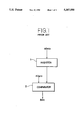
- FIG. 1 of the accompanying drawings shows a conventional break address detecting circuit for breaking the execution of a program.
- the conventional break address detecting circuit has a register 1 for holding and outputting a stop address ADstp where the operation of a processor is to be halted, and a comparator 2 for outputting a break signal BRK when an address ADpro of a program that is run by the processor (hereinafter referred to as a "program address ADpro") is compared and agrees with the output signal from the register 1, i.e., the stop address ADstp.
- an address where a program break is to occur is transferred to the register 1. Then, the processor is reset to start the program. The processor successively executes instructions in the sequence according to the program. At this time, program addresses that are successively executed by the processor are addresses in a program memory from which the program is read.
- the program addresses ADpro are successively inputted to the comparator 2.
- the comparator 2 compares the stop address ADstp held in the register with the program addresses ADpro. When the stop address ADstp agrees with one of the program addresses ADpro, the comparator 2 outputs a break signal BRK of an active level, breaking the operation of the processor.
- the step-by-step operation is essentially the same as the above breaking operation.
- an address of the program which is to be executed next to the address where the program is halted is stored in the register 1, and the processor is reset from the broken condition to execute the program from the start.
- the break is canceled and an instruction line next to the break is executed, whereupon the execution of the program is interrupted again.
- the above process is repeated a desired number of times.
- a breakpoint is indicated by a program address
- a program contains a branch instruction to cause execution to jump to a later address or a loop instruction to repeat the same instruction a plurality of times
- the program is halted when the instruction is executed for the first time, and it is impossible to break the program after the loop instruction is executed a desired number of times.
- an execution address at the time the step is executed can only be determined by carrying out the step-by-step operation successively and counting the steps. Such a process is complex and the execution time is very long.
- Another object of the present invention is to provide a break address detecting circuit which makes it unnecessary for a debugging controller to know the next program address to be executed in decoding instruction according to the step-by-step operation.
- Still another object of the present invention is to provide a break address detecting circuit which allows simplification of the arrangement of a debugging controller and which has a very high processing speed when a break is to occur a certain period of time after an instruction is executed.
- a break address detecting circuit comprising first data holding means for holding and outputting first data of a predetermined value, first counter means initializable by a reset signal for counting clock pulses in synchronism with a clock signal and for outputting counted data, selector means for selecting and outputting one program address and output data from the first counter means in response to a selection signal, first comparator means for comparing output data from the selector means and output data from the first data holding means and for outputting a comparison result signal which is of an active level when the compared data agree with each other, second counter means initializable by the reset signal for counting the comparison result signal each time the comparison result signal is of an active level and for outputting counted data, second data holding means for holding and outputting second data of a predetermined value, and second comparator means for comparing output data from the second data holding means and output data from the second counter means, and outputting a break signal which is of an active level when the compared data agree with each other.
- a break address detecting circuit comprising first data holding means for holding and outputting first data of a predetermined value, first comparator means for comparing output data from the first data holding means and a program address and for outputting a comparison result signal which is of an active level when the compared data and program address agree with each other, selector means for selecting in response to a selection signal either the comparison result signal or a clock signal which repeatedly alternates between active and inactive levels with predetermined timing, counter means initializable by a reset signal for counting output data from the selector means each time the output from the selector means is of an active level and for outputting counted data, second data holding means for holding and outputting second data of a predetermined value, and second comparator means for comparing output data from the second data holding means and output data from the counter means and outputting a break signal which is of an active level when the compared data agree each other.
- FIG. 1 is a block diagram of a conventional break address detecting circuit
- FIG. 2 is a block diagram of a break address detecting circuit according to a first embodiment of the present invention.
- FIG. 3 is a block diagram of a break address detecting circuit according to a second embodiment of the present invention.
- a break address detecting circuit has a register 1a for holding and outputting first data ADstp (hereinafter referred to as a "stop address ADstp") of a predetermined value; a first counter 3a which is initialized by a reset signal RST and counts up clock pulses in synchronism with a clock signal CKcyc (hereinafter referred to as an "instruction cycle clock signal CKcyc”) indicating an instruction execution cycle, and outputs counted data; a selector 4a for selecting and outputting one program address ADpro being executed and the output data from the first counter 3a in response to a selection signal SL; and a first comparator 2a which compares the output data from the selector 4a and the output data from the register 1a and outputs a comparison result signal CR which is of an active level when the compared data agree with each other.
- CKcyc clock signal
- the break address detecting circuit also includes a second counter 3b which is initialized by the reset signal RST, counts up the comparison result signal CR each time the comparison result signal CR is of an active level, and outputs counted data; a register 1b for holding and outputting second data CVstp (hereinafter referred to as a "stop count CVstp") of a predetermined value; and a second comparator 2b which compares the output data from the register 1b and the output data from the second counter 3b and outputs a break signal BRK which is of an active level when the compared data agree with each other.
- a second counter 3b which is initialized by the reset signal RST, counts up the comparison result signal CR each time the comparison result signal CR is of an active level, and outputs counted data
- a register 1b for holding and outputting second data CVstp (hereinafter referred to as a "stop count CVstp") of a predetermined value
- a second comparator 2b which compares the
- an address where a program break is to occur i.e., a stop address ADstp
- a stop count CVstp of "1" is stored in the register 1b.
- the selector 4a is controlled to select a program address ADpro by the selection signal SL.
- the program can now start to be executed by resetting the processor, i.e., making active the reset signal RST.
- the reset signal RST is applied to the first and second counters 3a, 3b, any data stored in these counters 3a, 3b is initialized to "0.”
- the program address ADpro is updated.
- the output signal, i.e., the comparison result signal CR, of the first comparator 2a is of an active level.
- the second counter 3b counts its data and holds and outputs a value of "1." Since this value is the same as the value held in the register 1b, the second comparator 2b outputs a break signal BRK of an active level, causing the processor to break the execution of the program.
- a program break is to occur after a certain instruction, such as a loop instruction or the like, is executed a plurality of times, the number of times that the certain instruction is to be executed, e.g., "3," is stored as the stop count CVstp in the register 1b.
- the processor is then reset to start the program and the second counter 3b is initialized.
- the program address ADpro agrees with the value stored in the register 1a
- the comparison result signal CR outputted by the first comparator 2a goes active in level
- the second counter 3b counts its data.
- the second counter 3b produces output data "3" that agrees with the value stored in the register 1b. Therefore, the second comparator 2b outputs a break signal BRK of an active level, causing the processor to break the execution of the program.
- the selection signal SL is applied to enable the selector 4a to select the output data from the first counter 3a.
- the data stored in the register 1a is not an address where a program break is to occur, but the number of instruction cycles that are to be executed after the program is started.
- the register 1b stores a value of "1.”
- the first and second counters 3a, 3b are initialized, and execution of the program begins.
- the first counter 3a counts the instruction cycle clock signal CKcyc.
- the comparison result signal CR outputted from the first comparator 2a goes active in level, and the second comparator 2b outputs a break signal BRK of an active level, causing the processor to break the execution of the program.
- the data stored in the register 1a is reset by adding "1" to the data that has been stored in the register 1a, following which either the processor is reset or the break is canceled. If the processor is reset, instruction cycles are executed from the start. If the break is canceled, the value stored in the first counter 3a agrees with the data stored in the register 1a when one instruction cycle is executed. The operation of the processor is interrupted and only one execution instruction line is executed. The above process has nothing to do with where the program address ADpro is located.
- the first counter 3a is set to this number of steps, because a program execution time can be calculated simply by multiplying an instruction execution cycle time by the number of steps. If a break is to occur again a certain period of time after a previous break, the first counter 3a is reset to a value which is the sum of the value that is in the first counter 3a and the number of steps.
- the number of bits of the second counter 3b which counts loops is small relatively to the first counter 3a which counts instruction steps.
- the counters 3a, 3b may be combined with each other with the counter 3b regarded as high-order bits of the counter 3a, and data may be set in advance in the register 1b, making it possible to count instruction execution cycles that are equal to cycles of the sum of bits of the counters 3a, 3b.
- FIG. 3 shows a break address detecting circuit according to a second embodiment of the present invention.
- the break address detecting circuit has a register 1a for holding and outputting first data ADstp (stop address ADstp) of a predetermined value; a first comparator 2c which compares the output data from the register 1a and a program address ADpro and outputs a comparison result signal CR which is of an active level when the compared data agree with each other, a selector 4b for selecting and outputting in response to a selection signal SL either the comparison result signal CR or an instruction cycle clock signal CKcyc which repeatedly alternates between active and inactive levels with predetermined timing; a counter 3b which is initialized by a reset signal RST and which counts up the output data from the selector 4b each time the output data from the selector 4b is of an active level and outputs counted data; a register 1b for holding and outputting second data (stop count CVstp) of a predetermined value; and a second comparator 2b which compares the output data from the register 1b and the output data from the counter 3
- the break address detecting circuit shown in FIG. 3 operates as follows:
- an address where a program break is to occur i.e., a stop address ADstp
- a stop count CVstp of "1" is stored in the register 1b.
- the selector 4b is controlled to select the comparison result signal CR outputted from the first comparator 2c.
- the processor is then reset, initializing the counter 3b and starting the program.
- the program address ADpro agrees with the stop address ADstp stored in the register 1a
- the comparison result signal CR from the first comparator 2c goes active in level.
- the counter 3b counts its data and holds and outputs a value of "1.”
- the second comparator 2b then outputs a break signal BRK of an active level causing the processor to break the execution of the program.
- the stop count CVstp is set to a desired number, as with the first embodiment.
- the selection signal SL is applied to enable the selector 4b to select the instruction cycle clock signal CKcyc.
- the number of steps is set in the register lb.
- the processor is now reset, initializing the counter 3b and starting the program.
- the counter 3b counts the instruction cycle clock signal CKcyc.
- the second comparator 2b outputs a break signal BRK of an active level, causing the processor to break the execution of the program.
- a program break after elapse of a desired period of time can be achieved by the break address detecting circuit shown in FIG. 3.
- the bit lengths of the register 1b, the second comparator 2b, and the counter 3b according to the second embodiment are larger than the bit lengths of the register 1b, the second comparator 2b, and the second counter 3b according to the first embodiment. This is because in the first embodiment, it is possible to reduce the bit lengths to a certain extent because they count only loops, and the counters 3a, 3b may be regarded as counters of high- and low-order bits in a counter of a large bit length in step-by-step operation, but the same large bit length has to be assigned to the counter 3b in the second embodiment. However, inasmuch as only one counter is employed, the circuit arrangement of the second embodiment is simpler than that of the first embodiment.
Abstract
Description
Claims (9)
Applications Claiming Priority (2)
| Application Number | Priority Date | Filing Date | Title |
|---|---|---|---|
| JP4-292838 | 1992-10-30 | ||
| JP4292838A JPH06139107A (en) | 1992-10-30 | 1992-10-30 | Brake address detecting circuit |
Publications (1)
| Publication Number | Publication Date |
|---|---|
| US5367550A true US5367550A (en) | 1994-11-22 |
Family
ID=17787017
Family Applications (1)
| Application Number | Title | Priority Date | Filing Date |
|---|---|---|---|
| US08/138,772 Expired - Lifetime US5367550A (en) | 1992-10-30 | 1993-10-19 | Break address detecting circuit |
Country Status (2)
| Country | Link |
|---|---|
| US (1) | US5367550A (en) |
| JP (1) | JPH06139107A (en) |
Cited By (27)
| Publication number | Priority date | Publication date | Assignee | Title |
|---|---|---|---|---|
| US5539795A (en) * | 1994-07-07 | 1996-07-23 | Nec Corporation | Sector pulse generating apparatus for multiple zone recording of a disk memory |
| US5566303A (en) * | 1993-05-31 | 1996-10-15 | Mitsubishi Denki Kabushiki Kaisha | Microcomputer with multiple CPU'S on a single chip with provision for testing and emulation of sub CPU's |
| US5621886A (en) * | 1995-06-19 | 1997-04-15 | Intel Corporation | Method and apparatus for providing efficient software debugging |
| US5659679A (en) * | 1995-05-30 | 1997-08-19 | Intel Corporation | Method and apparatus for providing breakpoints on taken jumps and for providing software profiling in a computer system |
| US5678003A (en) * | 1995-10-20 | 1997-10-14 | International Business Machines Corporation | Method and system for providing a restartable stop in a multiprocessor system |
| US5687389A (en) * | 1993-12-22 | 1997-11-11 | Adaptec, Inc. | System for controlling an automatic read operation of read cache control circuit in a disk drive controller utilizing a start counter, a working counter, and a sector counter |
| US5717851A (en) * | 1994-08-15 | 1998-02-10 | Motorola, Inc. | Breakpoint detection circuit in a data processor and method therefor |
| US5740413A (en) * | 1995-06-19 | 1998-04-14 | Intel Corporation | Method and apparatus for providing address breakpoints, branch breakpoints, and single stepping |
| US5774724A (en) * | 1995-11-20 | 1998-06-30 | International Business Machines Coporation | System and method for acquiring high granularity performance data in a computer system |
| US5838896A (en) * | 1995-12-31 | 1998-11-17 | Lg Semicon Co., Ltd. | Central processing unit for preventing program malfunction |
| US5933626A (en) * | 1997-06-12 | 1999-08-03 | Advanced Micro Devices, Inc. | Apparatus and method for tracing microprocessor instructions |
| US5944841A (en) * | 1997-04-15 | 1999-08-31 | Advanced Micro Devices, Inc. | Microprocessor with built-in instruction tracing capability |
| US5964893A (en) * | 1995-08-30 | 1999-10-12 | Motorola, Inc. | Data processing system for performing a trace function and method therefor |
| US6052801A (en) * | 1995-05-10 | 2000-04-18 | Intel Corporation | Method and apparatus for providing breakpoints on a selectable address range |
| US6249907B1 (en) | 1998-03-24 | 2001-06-19 | International Business Machines Corporation | Method system and article of manufacture for debugging a computer program by encoding user specified breakpoint types at multiple locations in the computer program |
| US20030061599A1 (en) * | 2001-09-26 | 2003-03-27 | International Business Machines Corporation | Dynamic setting of breakpoint count attributes |
| US20030217354A1 (en) * | 2002-05-16 | 2003-11-20 | International Business Machines Corporation | Scope-based breakpoint selection and operation |
| US6658557B1 (en) | 2000-05-25 | 2003-12-02 | Advanced Micro Devices, Inc. | Synthesizing the instruction stream executed by a microprocessor from its branch trace data |
| US6751751B1 (en) | 2000-11-06 | 2004-06-15 | Xilinx, Inc. | Universal multi-bus breakpoint unit for a configurable system-on-chip |
| US6757846B1 (en) * | 2000-11-06 | 2004-06-29 | Xilinx, Inc. | Method and apparatus for multi-bus breakpoint stepping |
| US6985980B1 (en) | 2000-11-03 | 2006-01-10 | Xilinx, Inc. | Diagnostic scheme for programmable logic in a system on a chip |
| US20060112241A1 (en) * | 2004-11-24 | 2006-05-25 | Yoav Weiss | System, method and apparatus of securing an operating system |
| US20080043897A1 (en) * | 2006-08-21 | 2008-02-21 | International Business Machines Corporation | Low latency counter event indication |
| US20080043899A1 (en) * | 2006-08-21 | 2008-02-21 | International Business Machines Corporation | Space and power efficient hybrid counters array |
| US20080046700A1 (en) * | 2006-08-21 | 2008-02-21 | International Business Machines Corporation | Method and apparatus for efficient performance monitoring of a large number of simultaneous events |
| US20090089547A1 (en) * | 2007-09-28 | 2009-04-02 | Moyer William C | System and method for monitoring debug events |
| US10176076B2 (en) * | 2013-08-23 | 2019-01-08 | Atmel Corporation | Breaking code execution based on time consumption |
Families Citing this family (1)
| Publication number | Priority date | Publication date | Assignee | Title |
|---|---|---|---|---|
| GB9825102D0 (en) * | 1998-11-16 | 1999-01-13 | Insignia Solutions Plc | Computer system |
Citations (8)
| Publication number | Priority date | Publication date | Assignee | Title |
|---|---|---|---|---|
| US5134701A (en) * | 1989-02-10 | 1992-07-28 | Hewlett-Packard Co. | Test apparatus performing runtime replacement of program instructions with breakpoint instructions for processor having multiple instruction fetch capabilities |
| US5253206A (en) * | 1990-03-30 | 1993-10-12 | Kabushiki Kaisha Toshiba | Electrically erasable programmable read-only memory with threshold value measurement circuit |
| US5257269A (en) * | 1989-12-04 | 1993-10-26 | Nec Corporation | Error controller for use in debugging microprocessor |
| US5265004A (en) * | 1991-10-15 | 1993-11-23 | Allen-Bradley Company, Inc. | Sequence controller with combinatorial Boolean logic |
| US5274831A (en) * | 1988-12-08 | 1993-12-28 | Nec Corporation | Microprocessor in response to an interrupt request for executing a microinstruction for sampling the mode of operation |
| US5301275A (en) * | 1991-10-03 | 1994-04-05 | Compaq Computer Corporation | Data transfer system with variable data buffer size and programmable interrupt frequency |
| US5311461A (en) * | 1988-12-30 | 1994-05-10 | International Business Machines Corp. | Programmable priority and selective blocking in a compute system |
| US5319645A (en) * | 1990-08-07 | 1994-06-07 | Bull Hn Information Systems Italia S.P.A. | Method for debugging and testing the correctness of programs |
Family Cites Families (2)
| Publication number | Priority date | Publication date | Assignee | Title |
|---|---|---|---|---|
| JPS53109455A (en) * | 1977-03-07 | 1978-09-25 | Hitachi Ltd | Debug control system |
| JPS63233442A (en) * | 1987-03-23 | 1988-09-29 | Toshiba Corp | Processor having debugging supporting circuit |
-
1992
- 1992-10-30 JP JP4292838A patent/JPH06139107A/en active Pending
-
1993
- 1993-10-19 US US08/138,772 patent/US5367550A/en not_active Expired - Lifetime
Patent Citations (8)
| Publication number | Priority date | Publication date | Assignee | Title |
|---|---|---|---|---|
| US5274831A (en) * | 1988-12-08 | 1993-12-28 | Nec Corporation | Microprocessor in response to an interrupt request for executing a microinstruction for sampling the mode of operation |
| US5311461A (en) * | 1988-12-30 | 1994-05-10 | International Business Machines Corp. | Programmable priority and selective blocking in a compute system |
| US5134701A (en) * | 1989-02-10 | 1992-07-28 | Hewlett-Packard Co. | Test apparatus performing runtime replacement of program instructions with breakpoint instructions for processor having multiple instruction fetch capabilities |
| US5257269A (en) * | 1989-12-04 | 1993-10-26 | Nec Corporation | Error controller for use in debugging microprocessor |
| US5253206A (en) * | 1990-03-30 | 1993-10-12 | Kabushiki Kaisha Toshiba | Electrically erasable programmable read-only memory with threshold value measurement circuit |
| US5319645A (en) * | 1990-08-07 | 1994-06-07 | Bull Hn Information Systems Italia S.P.A. | Method for debugging and testing the correctness of programs |
| US5301275A (en) * | 1991-10-03 | 1994-04-05 | Compaq Computer Corporation | Data transfer system with variable data buffer size and programmable interrupt frequency |
| US5265004A (en) * | 1991-10-15 | 1993-11-23 | Allen-Bradley Company, Inc. | Sequence controller with combinatorial Boolean logic |
Cited By (42)
| Publication number | Priority date | Publication date | Assignee | Title |
|---|---|---|---|---|
| US5566303A (en) * | 1993-05-31 | 1996-10-15 | Mitsubishi Denki Kabushiki Kaisha | Microcomputer with multiple CPU'S on a single chip with provision for testing and emulation of sub CPU's |
| US5687389A (en) * | 1993-12-22 | 1997-11-11 | Adaptec, Inc. | System for controlling an automatic read operation of read cache control circuit in a disk drive controller utilizing a start counter, a working counter, and a sector counter |
| US5539795A (en) * | 1994-07-07 | 1996-07-23 | Nec Corporation | Sector pulse generating apparatus for multiple zone recording of a disk memory |
| US5717851A (en) * | 1994-08-15 | 1998-02-10 | Motorola, Inc. | Breakpoint detection circuit in a data processor and method therefor |
| US6052801A (en) * | 1995-05-10 | 2000-04-18 | Intel Corporation | Method and apparatus for providing breakpoints on a selectable address range |
| US5659679A (en) * | 1995-05-30 | 1997-08-19 | Intel Corporation | Method and apparatus for providing breakpoints on taken jumps and for providing software profiling in a computer system |
| US5621886A (en) * | 1995-06-19 | 1997-04-15 | Intel Corporation | Method and apparatus for providing efficient software debugging |
| US5740413A (en) * | 1995-06-19 | 1998-04-14 | Intel Corporation | Method and apparatus for providing address breakpoints, branch breakpoints, and single stepping |
| US5964893A (en) * | 1995-08-30 | 1999-10-12 | Motorola, Inc. | Data processing system for performing a trace function and method therefor |
| US5678003A (en) * | 1995-10-20 | 1997-10-14 | International Business Machines Corporation | Method and system for providing a restartable stop in a multiprocessor system |
| US5774724A (en) * | 1995-11-20 | 1998-06-30 | International Business Machines Coporation | System and method for acquiring high granularity performance data in a computer system |
| US5838896A (en) * | 1995-12-31 | 1998-11-17 | Lg Semicon Co., Ltd. | Central processing unit for preventing program malfunction |
| US5944841A (en) * | 1997-04-15 | 1999-08-31 | Advanced Micro Devices, Inc. | Microprocessor with built-in instruction tracing capability |
| US5933626A (en) * | 1997-06-12 | 1999-08-03 | Advanced Micro Devices, Inc. | Apparatus and method for tracing microprocessor instructions |
| US6249907B1 (en) | 1998-03-24 | 2001-06-19 | International Business Machines Corporation | Method system and article of manufacture for debugging a computer program by encoding user specified breakpoint types at multiple locations in the computer program |
| US6658557B1 (en) | 2000-05-25 | 2003-12-02 | Advanced Micro Devices, Inc. | Synthesizing the instruction stream executed by a microprocessor from its branch trace data |
| US6985980B1 (en) | 2000-11-03 | 2006-01-10 | Xilinx, Inc. | Diagnostic scheme for programmable logic in a system on a chip |
| US6751751B1 (en) | 2000-11-06 | 2004-06-15 | Xilinx, Inc. | Universal multi-bus breakpoint unit for a configurable system-on-chip |
| US6757846B1 (en) * | 2000-11-06 | 2004-06-29 | Xilinx, Inc. | Method and apparatus for multi-bus breakpoint stepping |
| US20030061599A1 (en) * | 2001-09-26 | 2003-03-27 | International Business Machines Corporation | Dynamic setting of breakpoint count attributes |
| US7047519B2 (en) * | 2001-09-26 | 2006-05-16 | International Business Machines Corporation | Dynamic setting of breakpoint count attributes |
| US20030217354A1 (en) * | 2002-05-16 | 2003-11-20 | International Business Machines Corporation | Scope-based breakpoint selection and operation |
| US7178135B2 (en) * | 2002-05-16 | 2007-02-13 | International Business Machines Corporation | Scope-based breakpoint selection and operation |
| US20060112241A1 (en) * | 2004-11-24 | 2006-05-25 | Yoav Weiss | System, method and apparatus of securing an operating system |
| WO2006056988A2 (en) * | 2004-11-24 | 2006-06-01 | Discretix Technologies Ltd. | System, method and apparatus of securing an operating system |
| WO2006056988A3 (en) * | 2004-11-24 | 2006-12-21 | Discretix Technologies Ltd | System, method and apparatus of securing an operating system |
| GB2435780A (en) * | 2004-11-24 | 2007-09-05 | Discretix Technologies Ltd | System,method and apparatus of securing an operating system |
| US20080046700A1 (en) * | 2006-08-21 | 2008-02-21 | International Business Machines Corporation | Method and apparatus for efficient performance monitoring of a large number of simultaneous events |
| US20090116611A1 (en) * | 2006-08-21 | 2009-05-07 | International Business Machines Corporation | Space and power efficient hybrid counters array |
| US20080043897A1 (en) * | 2006-08-21 | 2008-02-21 | International Business Machines Corporation | Low latency counter event indication |
| US7426253B2 (en) * | 2006-08-21 | 2008-09-16 | International Business Machines Corporation | Low latency counter event indication |
| US7461383B2 (en) * | 2006-08-21 | 2008-12-02 | International Business Machines Corporation | Method and apparatus for efficient performance monitoring of a large number of simultaneous events |
| US20090077571A1 (en) * | 2006-08-21 | 2009-03-19 | International Business Machines Corporation | Method and apparatus for efficient performance monitoring of a large number of simultaneous events |
| US7877759B2 (en) | 2006-08-21 | 2011-01-25 | International Business Machines Corporation | System for efficient performance monitoring of a large number of simultaneous events |
| US20080043899A1 (en) * | 2006-08-21 | 2008-02-21 | International Business Machines Corporation | Space and power efficient hybrid counters array |
| US20090116610A1 (en) * | 2006-08-21 | 2009-05-07 | International Business Machines Corporation | Low latency counter event indication |
| US7532700B2 (en) * | 2006-08-21 | 2009-05-12 | International Business Machines Corporation | Space and power efficient hybrid counters array |
| US7688931B2 (en) * | 2006-08-21 | 2010-03-30 | International Business Machines Corporation | Space and power efficient hybrid counters array |
| US7782995B2 (en) * | 2006-08-21 | 2010-08-24 | International Business Machines Corporation | Low latency counter event indication |
| US20090089547A1 (en) * | 2007-09-28 | 2009-04-02 | Moyer William C | System and method for monitoring debug events |
| US8407457B2 (en) | 2007-09-28 | 2013-03-26 | Freescale Semiconductor, Inc. | System and method for monitoring debug events |
| US10176076B2 (en) * | 2013-08-23 | 2019-01-08 | Atmel Corporation | Breaking code execution based on time consumption |
Also Published As
| Publication number | Publication date |
|---|---|
| JPH06139107A (en) | 1994-05-20 |
Similar Documents
| Publication | Publication Date | Title |
|---|---|---|
| US5367550A (en) | Break address detecting circuit | |
| US5596760A (en) | Program control method and program control apparatus | |
| US4763296A (en) | Watchdog timer | |
| US4365311A (en) | Control of instruction pipeline in data processing system | |
| US5715435A (en) | Trace control circuit in emulation system | |
| KR100233188B1 (en) | Computer system capable of outputing status data without interrupting execution of program | |
| EP1125199B1 (en) | Method of debugging a program thread | |
| RU2001130347A (en) | Protecting the core of a computing device from unauthorized changes from the outside | |
| KR100521110B1 (en) | Event handling | |
| JP2002152020A (en) | Pulse signal generator | |
| JPH10275092A (en) | Trace information output method for microprocessor | |
| US5664167A (en) | Microprogrammed timer processor having a variable loop resolution architecture | |
| US20030204707A1 (en) | Real-time tracing microprocessor unit and operating method | |
| KR100284287B1 (en) | Microprocessor with Variable Reset Address | |
| US5325514A (en) | Program executive timing apparatus for ensuring that state changes of a reference clock signal used to time the execution of the program are not missed | |
| US6850879B1 (en) | Microcomputer with emulator interface | |
| JP2001060162A (en) | In-circuit emulator | |
| JP2001092692A (en) | Circuit and method for measuring time | |
| JP2758624B2 (en) | Speed control method of micro program | |
| JPS60124746A (en) | Data processing unit | |
| JP2718402B2 (en) | Time measurement circuit for built-in in-circuit emulator | |
| SU1509901A1 (en) | Arrangement for monitoring digital devices | |
| JP2631541B2 (en) | Programmable controller | |
| JP2001337847A (en) | Processor circuit | |
| JPS63639A (en) | Program debugging system |
Legal Events
| Date | Code | Title | Description |
|---|---|---|---|
| AS | Assignment |
Owner name: NEC CORPORATION, JAPAN Free format text: ASSIGNMENT OF ASSIGNORS INTEREST;ASSIGNOR:ISHIDA, RYUJI;REEL/FRAME:006738/0601 Effective date: 19931012 |
|
| STCF | Information on status: patent grant |
Free format text: PATENTED CASE |
|
| FEPP | Fee payment procedure |
Free format text: PAYOR NUMBER ASSIGNED (ORIGINAL EVENT CODE: ASPN); ENTITY STATUS OF PATENT OWNER: LARGE ENTITY |
|
| FPAY | Fee payment |
Year of fee payment: 4 |
|
| FPAY | Fee payment |
Year of fee payment: 8 |
|
| AS | Assignment |
Owner name: NEC ELECTRONICS CORPORATION, JAPAN Free format text: ASSIGNMENT OF ASSIGNORS INTEREST;ASSIGNOR:NEC CORPORATION;REEL/FRAME:013758/0440 Effective date: 20021101 |
|
| FPAY | Fee payment |
Year of fee payment: 12 |
|
| AS | Assignment |
Owner name: RENESAS ELECTRONICS CORPORATION, JAPAN Free format text: CHANGE OF NAME;ASSIGNOR:NEC ELECTRONICS CORPORATION;REEL/FRAME:025148/0010 Effective date: 20100401 |